unit iv wave shaping and multivibrator circuits - Jeppiaar ...
43
EC8452: Electronic Circuits-II Department of ECE 2020 - 2021 1 Jeppiaar Institute of Technology UNIT IV WAVE SHAPING AND MULTIVIBRATOR CIRCUITS Pulse circuits – attenuators – RC integrator and differentiator circuits – diode clampers and clippers –Multivibrators - Schmitt Trigger- UJT Oscillator. WAVE SHAPING AND MULTIVIBRATOR CIRCUITS Linear wave shaping :Process by which the shape of a non sinusoidal signal is changed by passing the signal through the network consisting of linear elements Diodes can be used in wave shapinga circuits. Either limit or clip signal portion--- clipper shift the dc voltage level of the signal --- clampers Types of non sinusoidal input Step pulse square Ramp input RL circuit RL circuit is used for small time constants. To get a large time constant the inductance value has to be chosen high Higher inductance value are provided by iron core inductors which are bigger in size, heavy and costly.
-
Upload
khangminh22 -
Category
Documents
-
view
2 -
download
0
Transcript of unit iv wave shaping and multivibrator circuits - Jeppiaar ...
EC8452: Electronic Circuits-II Department of ECE
2020 - 2021 1 Jeppiaar Institute of Technology
UNIT IV
WAVE SHAPING AND MULTIVIBRATOR CIRCUITS
Pulse circuits – attenuators – RC integrator and differentiator circuits – diode
clampers and clippers –Multivibrators - Schmitt Trigger- UJT Oscillator.
WAVE SHAPING AND MULTIVIBRATOR CIRCUITS
Linear wave shaping :Process by which the shape of a non sinusoidal signal is
changed by passing the signal through the network consisting of linear elements
Diodes can be used in wave shapinga circuits.
Either limit or clip signal portion--- clipper
shift the dc voltage level of the signal --- clampers
Types of non sinusoidal input
Step
pulse
square
Ramp input
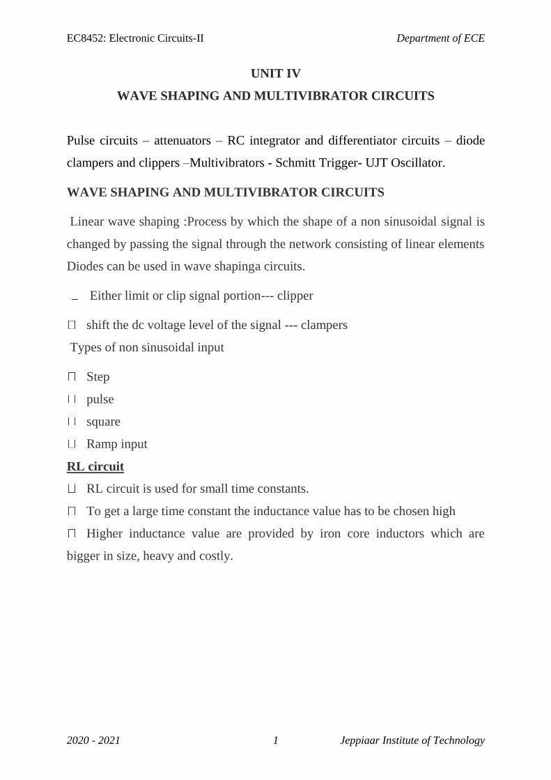
RL circuit
RL circuit is used for small time constants.
To get a large time constant the inductance value has to be chosen high
Higher inductance value are provided by iron core inductors which are
bigger in size, heavy and costly.
EC8452: Electronic Circuits-II Department of ECE
2020 - 2021 1 Jeppiaar Institute of Technology
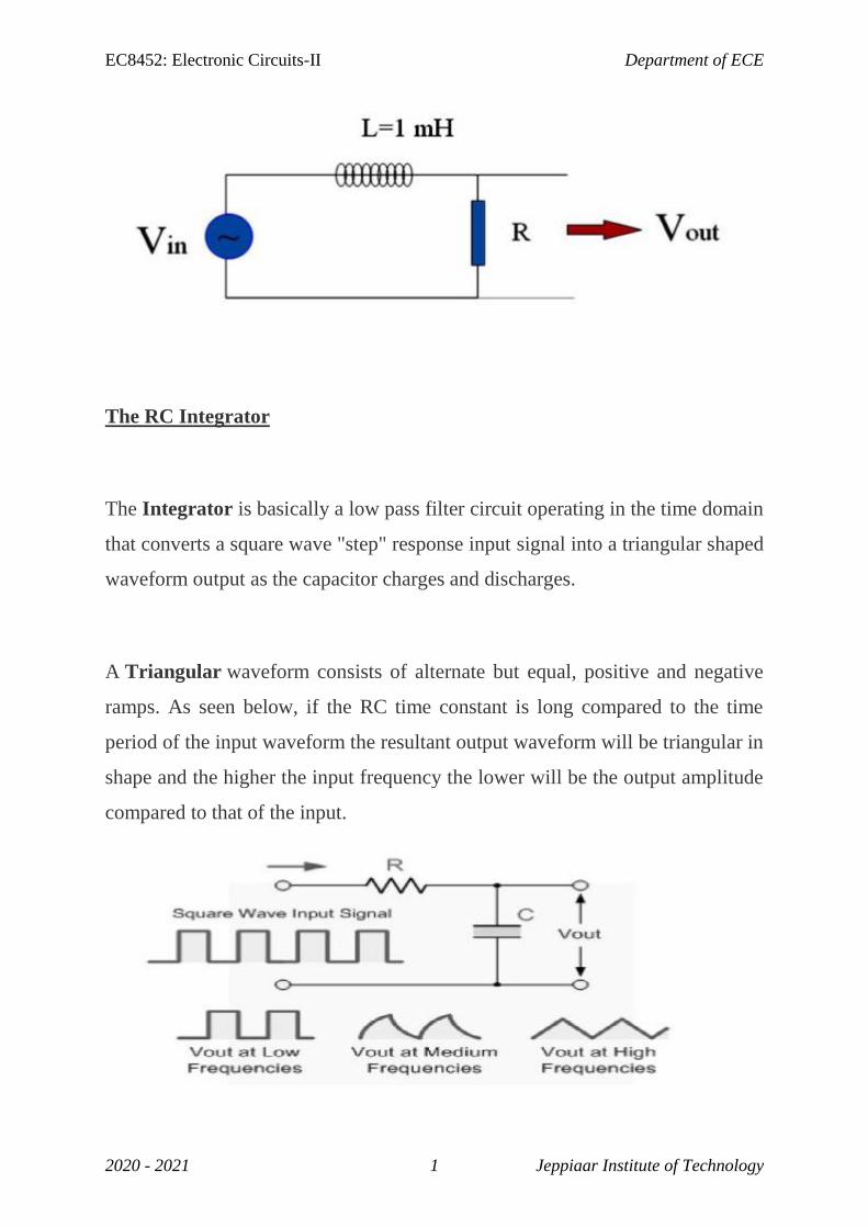
The RC Integrator
The Integrator is basically a low pass filter circuit operating in the time domain
that converts a square wave "step" response input signal into a triangular shaped
waveform output as the capacitor charges and discharges.
A Triangular waveform consists of alternate but equal, positive and negative
ramps. As seen below, if the RC time constant is long compared to the time
period of the input waveform the resultant output waveform will be triangular in
shape and the higher the input frequency the lower will be the output amplitude
compared to that of the input.
EC8452: Electronic Circuits-II Department of ECE
2020 - 2021 1 Jeppiaar Institute of Technology
This then makes this type of circuit ideal for converting one type of electronic
signal to another for use in wave-generating or wave-shaping circuits.
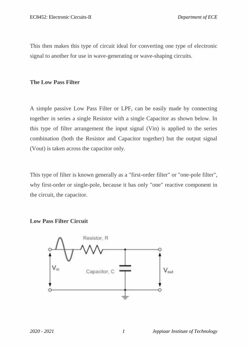
The Low Pass Filter
A simple passive Low Pass Filter or LPF, can be easily made by connecting
together in series a single Resistor with a single Capacitor as shown below. In
this type of filter arrangement the input signal (Vin) is applied to the series
combination (both the Resistor and Capacitor together) but the output signal
(Vout) is taken across the capacitor only.
This type of filter is known generally as a "first-order filter" or "one-pole filter",
why first-order or single-pole, because it has only "one" reactive component in
the circuit, the capacitor.
Low Pass Filter Circuit
EC8452: Electronic Circuits-II Department of ECE
2020 - 2021 1 Jeppiaar Institute of Technology
The reactance of a capacitor varies inversely with frequency, while the value of
the resistor remains constant as the frequency changes. At low frequencies the
capacitive reactance, (Xc) of the capacitor will be very large compared to the
resistive value of the resistor, R and as a result the voltage across the capacitor,
Vc will also be large while the voltage drop across the resistor, Vr will be much
lower. At high frequencies the reverse is true with Vc being small and Vr being
large.
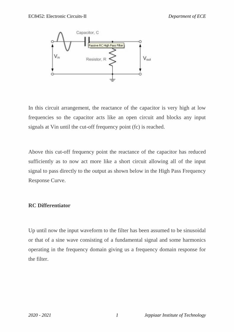
High Pass Filters
A High Pass Filter or HPF, is the exact opposite to that of the Low Pass filter
circuit, as now the two components have been interchanged with the output
signal (Vout) being taken from across the resistor as shown.
Where the low pass filter only allowed signals to pass below its cut-off
frequency point, fc. The passive high pass filter circuit as its name implies, only
passes signals above the selected cut-off point, fc eliminating any low frequency
signals from the waveform. Consider the circuit below.
The High Pass Filter Circuit
EC8452: Electronic Circuits-II Department of ECE
2020 - 2021 1 Jeppiaar Institute of Technology
In this circuit arrangement, the reactance of the capacitor is very high at low
frequencies so the capacitor acts like an open circuit and blocks any input
signals at Vin until the cut-off frequency point (fc) is reached.
Above this cut-off frequency point the reactance of the capacitor has reduced
sufficiently as to now act more like a short circuit allowing all of the input
signal to pass directly to the output as shown below in the High Pass Frequency
Response Curve.
RC Differentiator
Up until now the input waveform to the filter has been assumed to be sinusoidal
or that of a sine wave consisting of a fundamental signal and some harmonics
operating in the frequency domain giving us a frequency domain response for
the filter.
EC8452: Electronic Circuits-II Department of ECE
2020 - 2021 1 Jeppiaar Institute of Technology
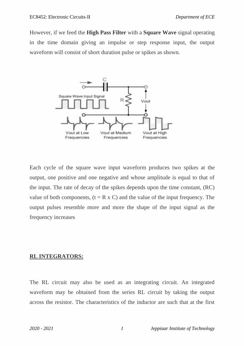
However, if we feed the High Pass Filter with a Square Wave signal operating
in the time domain giving an impulse or step response input, the output
waveform will consist of short duration pulse or spikes as shown.
Each cycle of the square wave input waveform produces two spikes at the
output, one positive and one negative and whose amplitude is equal to that of
the input. The rate of decay of the spikes depends upon the time constant, (RC)
value of both components, (t = R x C) and the value of the input frequency. The
output pulses resemble more and more the shape of the input signal as the
frequency increases
RL INTEGRATORS:
The RL circuit may also be used as an integrating circuit. An integrated
waveform may be obtained from the series RL circuit by taking the output
across the resistor. The characteristics of the inductor are such that at the first
EC8452: Electronic Circuits-II Department of ECE
2020 - 2021 1 Jeppiaar Institute of Technology
instant of time in which voltage is applied, current flow through the inductor is
minimum and the voltage developed across it is maximum.
Therefore, the value of the voltage drop across the series resistor at that first
instant must be 0 volts because there is no current flow through it. As time
passes, current begins to flow through the circuit and voltage develops across
the resistor. Since the circuit has a long time constant, the voltage across the
resistor does NOT respond to the rapid changes in voltage of the input square
wave. Therefore, the conditions for integration in an RL circuit are a long time
constant with the output taken across the resistor.
There are a variety of diode network called clippers that have the ability to-
―clip‖ off a portion of the input signal without distorting the remaining part of
the alternating waveform. The half wave rectifier is an example of the simplest
form of diode clipper one resistor and diode.
Depending on the orientation of the diode, the positive or negative region of the
input signal is- ―clipped‖ off. There are two general categories of clippers:
series and parallel. The series configuration is defined as one where the diode is
in series with the load, while the parallel variety has the diode in a branch
parallel to the load.
Multivibrators
Introduction
EC8452: Electronic Circuits-II Department of ECE
2020 - 2021 1 Jeppiaar Institute of Technology
The type of circuit most often used to generate square or rectangular waves is
the multivibrator. A multivibrator, is basically two amplifier circuits arranged
with regenerative feedback. One of the amplifiers is conducting while the other
is cut off When an input signal to one amplifier is large enough, the transistor
can be driven into cutoff, and its collector voltage will be almost V CC.
However, when the transistor is driven into saturation, its collector voltage will
be about 0 volts.
A circuit that is designed to go quickly from cutoff to saturation will produce a
square or rectangular wave at its output. This principle is used in multivibrators.
Multivibrators are classified according to the number of steady (stable) states of
the circuit. A steady state exists when circuit operation is essentially constant;
that is, one transistor remains in conduction and the other remains cut off until
an external signal is applied.
The three types of multivibrators :
ASTABLE
MONOSTABLE
BISTABLE.
The astable circuit has no stable state. With no external signal applied, the
transistors alternately switch from cutoff to saturation at a frequency determined
by the RC time constants of the coupling circuits.
The monostable circuit has one stable state; one transistor conducts while the
other is cut off. A signal must be applied to change this condition. After a
EC8452: Electronic Circuits-II Department of ECE
2020 - 2021 1 Jeppiaar Institute of Technology
period of time, determined by the internal RC components, the circuit will
return to its original condition where it remains until the next signal arrives.
The bistable multivibrator has two stable states. It remains in one of the stable
states until a trigger is applied. It then FLIPS to the other stable condition and
remains there until another trigger is applied. The multivibrator then changes
back (FLOPS) to its first stable state.
1. Astable Multivibrator
A multivibrator which generates square waves of its own (i.e. without any
external trigger pulse) is known as astable multivibrator. It is also called free
ramming multivibrator. It has no stable state but only two quasi-stables (half-
stable) makes oscillating continuously between these states. Thus it is just an
oscillator since it requires no external pulse for its operation of course it does
require D.C power.
In such circuit neither of the two transistors reaches a stable state. It switches
back and forth from one state to the other, remaining in each state for a time
determined by circuit constants. In other words, at first one transistor conducts
(i.e. ON state) and the other stays in the OFF state for some time. After this
period of time, the second transistor is automatically turned ON and the first
transistor turned OFF. Thus the multivibrator will generate a square wave of its
own. The width of the square wave and it frequency will depend upon the
circuit constants.
EC8452: Electronic Circuits-II Department of ECE
2020 - 2021 1 Jeppiaar Institute of Technology
Here we like to describe.
Collector - coupled Astabe multivibrator
Emitter - coupled Astable multivibrator
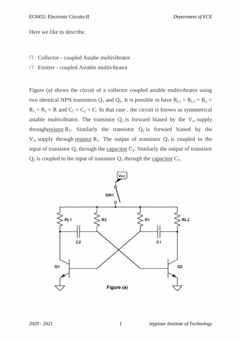
Figure (a) shows the circuit of a collector coupled astable multivibrator using
two identical NPN transistors Q1 and Q2. It is possible to have RL1 = RL2 = RL =
R1 = R2 = R and C1 = C2 = C. In that case , the circuit is known as symmetrical
astable multivibrator. The transistor Q1 is forward biased by the Vcc supply
throughresistor R2. Similarly the transistor Q2 is forward biased by the
Vcc supply through resistor R1. The output of transistor Q1 is coupled to the
input of transistor Q2 through the capacitor C2. Similarly the output of transistor
Q2 is coupled to the input of transistor Q1 through the capacitor C1.
EC8452: Electronic Circuits-II Department of ECE
2020 - 2021 1 Jeppiaar Institute of Technology
It consists of two common emitter amplifying stages. Each stage provides a
feedback through a capacitor at the input of the other. Since the amplifying
stage introduces a 180o phase shift and another 180
o phase shift is introduced by
a capacitor, therefore the feedback signal and the circuit works as an oscillator.
In other words because of capacitive coupling none of the transistor can remain
permanently out-off or saturated, instead of circuit has two quasi-stable states
(ON and OFF) and it makes periodic transition between these two states.
The output of an Astable multivibrator is available at the collector terminal of
the either transistors as shown in figure (a). However, the two outputs are
180o out of phase with each other. Therefore one of the outputs is said to be the
complement of the other.
Let us suppose that
When Q1is ON, Q2 is OFF and
When Q2 is ON, Q1 is OFF.
When the D.C power supply is switched ON by closing S, one of the transistors
will start conducting before the other (or slightly faster than the other). It is so
because characteristics of no two similar transistors can be exactly alike
suppose that Q1 starts conducting before Q2 does. The feedback system is such
that Q1 will be very rapidly driven ton saturation and Q2 to cut-off. The circuit
operation may be explained as follows.
EC8452: Electronic Circuits-II Department of ECE
2020 - 2021 1 Jeppiaar Institute of Technology
Since Q1 is in saturation whole of VCC drops across RL1. Hence VC1 = 0 and
point A is at zero or ground potential. Since Q2 is in cut-off i.e. it conducts no
current, there is no drop across R L2. Hence point B is at VCC. Since A is at 0V
C2 starts to charge through R2 towards VCC.
When voltage across C2 rises sufficiently (i.e. more than 0.7V), it biases Q2 in
the forward direction so that it starts conducting and is soon driven to saturation.
VCC decreases and becomes almost zero when Q2 gets saturated. The potential
of point B decreases from VCC to almost 0V. This potential decrease (negative
swing) is applied to the base of Q1 through C1. Consequently, Q1 is pulled out of
saturation and is soon driven to cut-off.
Since, now point B is at 0V, C1 starts charging through R1 towards the target
voltage VCC.
When voltage of C1 increases sufficiently. Q1 becomes forward-biased and
starts conducting. In this way the whole cycle is repeated.
It is observed that the circuit alternates between a state in which Q1 is ON and
Q2 is OFF and the state in which Q1 is OFF and Q2 is ON. This time in each
state depends on RC values. Since each transistor is driven alternately into
saturation and cut-off. The voltage waveform at either collector (points A and B
in figure (b)) is essentially a square waveform with peak amplitude equal to
VCC.
EC8452: Electronic Circuits-II Department of ECE
2020 - 2021 1 Jeppiaar Institute of Technology
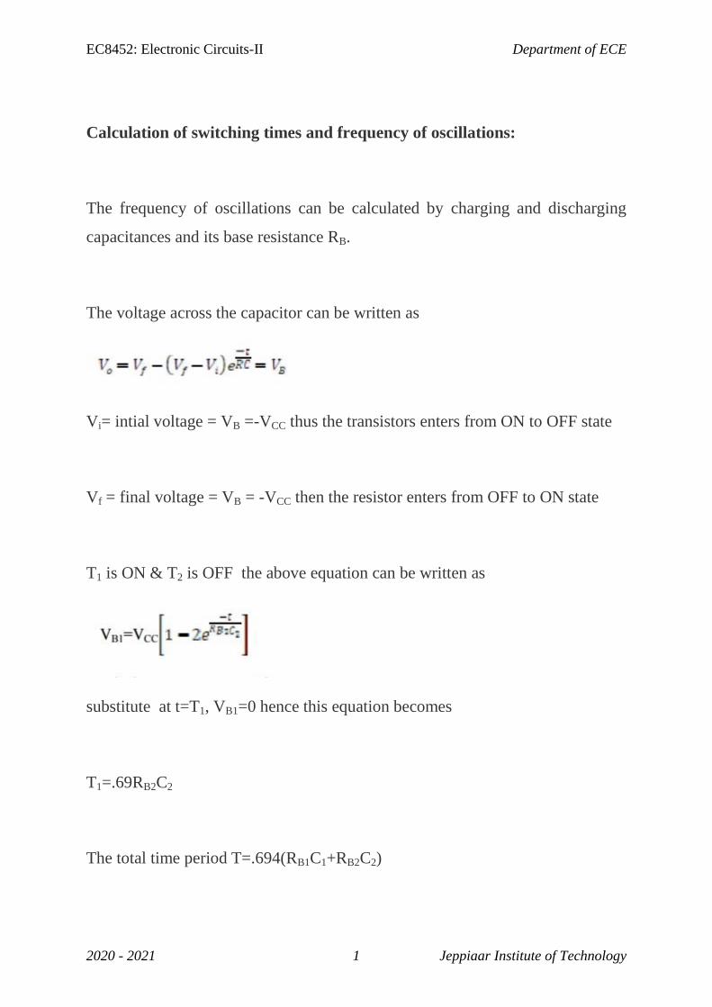
Calculation of switching times and frequency of oscillations:
The frequency of oscillations can be calculated by charging and discharging
capacitances and its base resistance RB.
The voltage across the capacitor can be written as
Vi= intial voltage = VB =-VCC thus the transistors enters from ON to OFF state
Vf = final voltage = VB = -VCC then the resistor enters from OFF to ON state
T1 is ON & T2 is OFF the above equation can be written as
substitute at t=T1, VB1=0 hence this equation becomes
T1=.69RB2C2
The total time period T=.694(RB1C1+RB2C2)
EC8452: Electronic Circuits-II Department of ECE
2020 - 2021 1 Jeppiaar Institute of Technology
When RB!=RB2=R & C1=C2=C
T=1.39RC
Frequency of free running multivibrator is given by
the frequency stability of the circuit is not good as only the function of the
product of RC but also depends on load resistances, supply voltages and circuit
parameters. In order to stabilize the frequency, synchronizing signals are
injected which terminate the unstable periods earlier than would occur naturally.
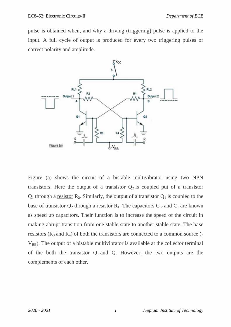
2. Bistable multivibrator
The bistable multivibrator has two absolutely stable states. It will remain in
whichever state it happens to be until a trigger pulse causes it to switch to the
other state. For instance, suppose at any particular instant,transistor Q1 is
conducting and transistor Q 2 is at cut-off. If left to itself, the bistable
multivibrator will stay in this position for ever. However, if an external pulse is
applied to the circuit in such a way that Q1 is cut-off and Q2 is turned on, the
circuit will stay in the new position. Another trigger pulse is then required to
switch the circuit back to its original state.
In other words a multivibrator which has both the state stable is called a bistable
multivibrator. It is also called flip-flop, trigger circuit or binary. The output
EC8452: Electronic Circuits-II Department of ECE
2020 - 2021 1 Jeppiaar Institute of Technology
pulse is obtained when, and why a driving (triggering) pulse is applied to the
input. A full cycle of output is produced for every two triggering pulses of
correct polarity and amplitude.
Figure (a) shows the circuit of a bistable multivibrator using two NPN
transistors. Here the output of a transistor Q2 is coupled put of a transistor
Q1 through a resistor R2. Similarly, the output of a transistor Q1 is coupled to the
base of transistor Q2 through a resistor R1. The capacitors C 2 and C1 are known
as speed up capacitors. Their function is to increase the speed of the circuit in
making abrupt transition from one stable state to another stable state. The base
resistors (R3 and R4) of both the transistors are connected to a common source (-
VBB). The output of a bistable multivibrator is available at the collector terminal
of the both the transistor Q1 and Q. However, the two outputs are the
complements of each other.
EC8452: Electronic Circuits-II Department of ECE
2020 - 2021 1 Jeppiaar Institute of Technology
Let us suppose, if Q1 is conducting, then the fact that point A is at nearly ON
makes the base of Q2 negative (by the potential divider R2 - R4) and holds
Q2 off.
Similarly with Q2 OFF, the potential divider from VCC to -VBB (RL2, R1, R3) is
designed to keep base of Q1at about 0.7V ensuring that Q1 conducts. It is seen
that Q1 holds Q2 OFF and Q2 hold Q1 ON. Suppose, now a positive pulse is
applied momentarily to R. It will cause Q2 to conduct. As collector of Q2 falls to
zero, it cuts Q1 OFF and consequently, the BMV switches over to its other state.
Similarly, a positive trigger pulse applied to S will switch the BMV back to its
original state.
Uses:
In timing circuits as frequency divider
In counting circuits
In computer memory circuits
Bistable Multivibrator Triggering
EC8452: Electronic Circuits-II Department of ECE
2020 - 2021 1 Jeppiaar Institute of Technology
To change the stable state of the binary it is necessary to apply an appropriate
pulse in the circuit, which will try to bring both the transistors to active region
and the resulting regenerative feedback will result on the change of state.
Triggering may be of two following types:
Asymmetrical triggering
Symmetrical triggering
(I) Asymmetrical triggering
In asymmetrical triggering, there are two trigger inputs for the transistors Q1 and
Q2. Each trigger input is derived from a separate triggering source. To induce
transition among the stable states, let us say that initially the trigger is applied to
the bistable. For the next transition, now the identical trigger must appear at the
transistor Q2. Thus it can be said that the asymmetrical triggering the trigger
pulses derived from two separate source and connected to the two transistors
Q1 and Q2 individually, sequentially change the state of the bistable.
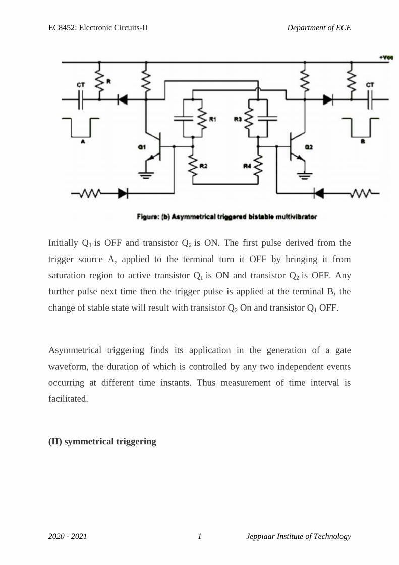
Figure (b) shows the circuit diagram of an asymmetrically triggered bistable
multivibrator.
EC8452: Electronic Circuits-II Department of ECE
2020 - 2021 1 Jeppiaar Institute of Technology
Initially Q1 is OFF and transistor Q2 is ON. The first pulse derived from the
trigger source A, applied to the terminal turn it OFF by bringing it from
saturation region to active transistor Q1 is ON and transistor Q2 is OFF. Any
further pulse next time then the trigger pulse is applied at the terminal B, the
change of stable state will result with transistor Q2 On and transistor Q1 OFF.
Asymmetrical triggering finds its application in the generation of a gate
waveform, the duration of which is controlled by any two independent events
occurring at different time instants. Thus measurement of time interval is
facilitated.
(II) symmetrical triggering
EC8452: Electronic Circuits-II Department of ECE
2020 - 2021 1 Jeppiaar Institute of Technology
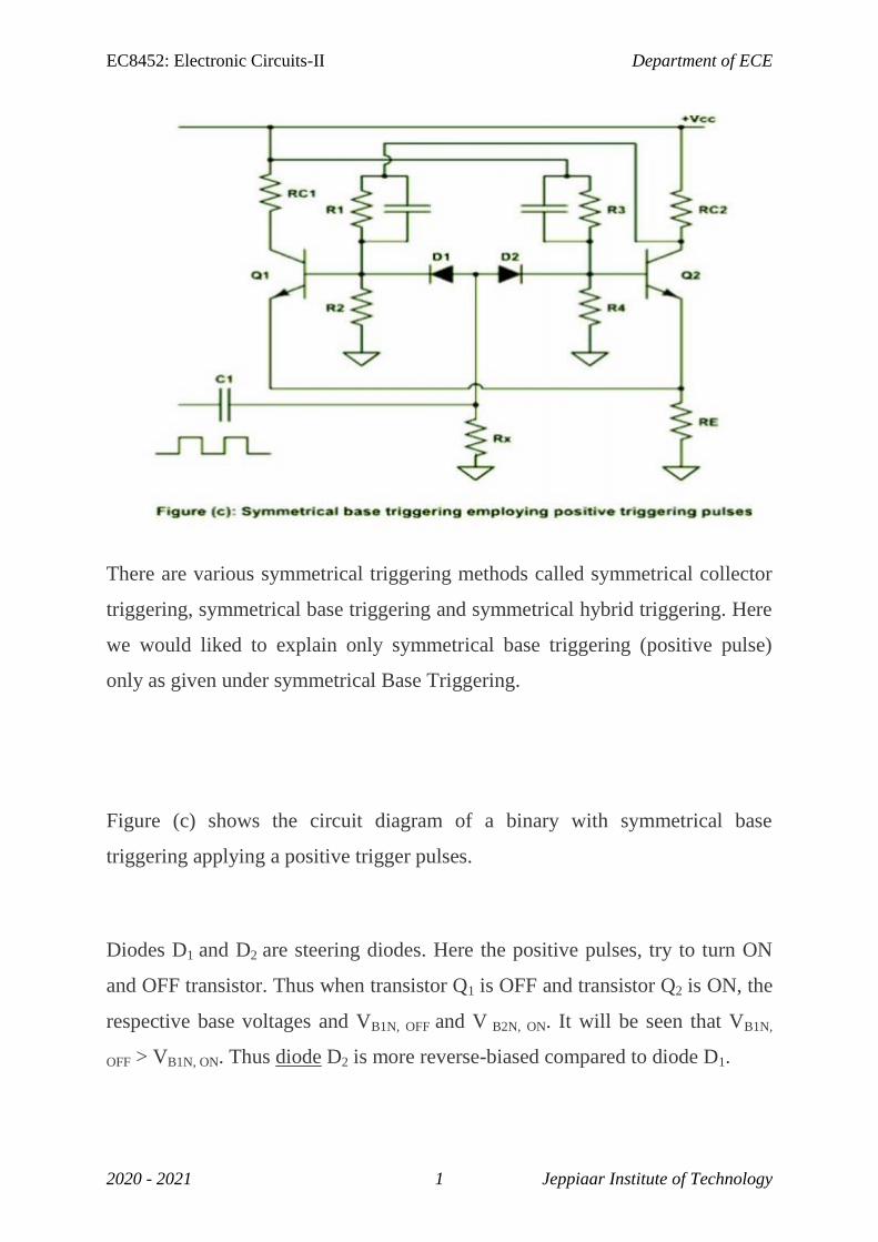
There are various symmetrical triggering methods called symmetrical collector
triggering, symmetrical base triggering and symmetrical hybrid triggering. Here
we would liked to explain only symmetrical base triggering (positive pulse)
only as given under symmetrical Base Triggering.
Figure (c) shows the circuit diagram of a binary with symmetrical base
triggering applying a positive trigger pulses.
Diodes D1 and D2 are steering diodes. Here the positive pulses, try to turn ON
and OFF transistor. Thus when transistor Q1 is OFF and transistor Q2 is ON, the
respective base voltages and VB1N, OFF and V B2N, ON. It will be seen that VB1N,
OFF > VB1N, ON. Thus diode D2 is more reverse-biased compared to diode D1.
EC8452: Electronic Circuits-II Department of ECE
2020 - 2021 1 Jeppiaar Institute of Technology
When the positive differentiated pulse of amplitude greater than (VB1N, OFF +
Vɣ) appears, the diode D1 gets forward biased, and transistor Q1 enters the
active region and with subsequent regenerative feedback Q1 gets ON, and
transistor Q2 becomes OFF. On the arrival of the next trigger pulse now the
diode D2 will be forward biased and ultimately with regenerative feedback it
will be in the ON state.
Clippers
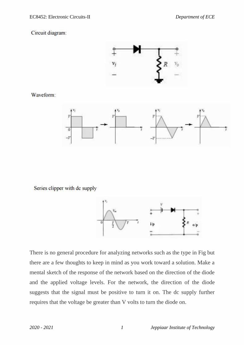
Series clipper
The response of the series configuration to a variety of alternating waveforms is
provided although first introduced as a half-wave rectifier (for sinusoidal
waveforms); there are no boundaries on the type of signals that can be applied
to a clipper. The addition of a dc supply can have a pronounced effect on the
output of a clipper. Our initial discussion will be limited to ideal diodes, with
the effect of VT reserved for a concluding example.
Circuit diagram:
EC8452: Electronic Circuits-II Department of ECE
2020 - 2021 1 Jeppiaar Institute of Technology
There is no general procedure for analyzing networks such as the type in Fig but
there are a few thoughts to keep in mind as you work toward a solution. Make a
mental sketch of the response of the network based on the direction of the diode
and the applied voltage levels. For the network, the direction of the diode
suggests that the signal must be positive to turn it on. The dc supply further
requires that the voltage be greater than V volts to turn the diode on.
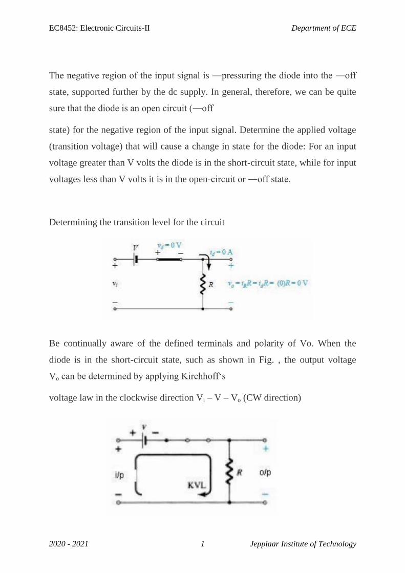
EC8452: Electronic Circuits-II Department of ECE
2020 - 2021 1 Jeppiaar Institute of Technology
The negative region of the input signal is ―pressuring the diode into the ―off
state, supported further by the dc supply. In general, therefore, we can be quite
sure that the diode is an open circuit (―off
state) for the negative region of the input signal. Determine the applied voltage
(transition voltage) that will cause a change in state for the diode: For an input
voltage greater than V volts the diode is in the short-circuit state, while for input
voltages less than V volts it is in the open-circuit or ―off state.
Determining the transition level for the circuit
Be continually aware of the defined terminals and polarity of Vo. When the
diode is in the short-circuit state, such as shown in Fig. , the output voltage
Vo can be determined by applying Kirchhoff‗s
voltage law in the clockwise direction Vi – V – Vo (CW direction)
EC8452: Electronic Circuits-II Department of ECE
2020 - 2021 1 Jeppiaar Institute of Technology
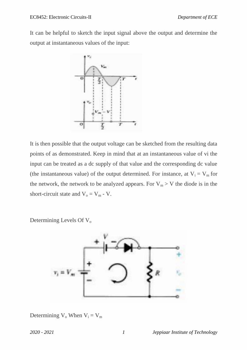
It can be helpful to sketch the input signal above the output and determine the
output at instantaneous values of the input:
It is then possible that the output voltage can be sketched from the resulting data
points of as demonstrated. Keep in mind that at an instantaneous value of vi the
input can be treated as a dc supply of that value and the corresponding dc value
(the instantaneous value) of the output determined. For instance, at Vi = Vm for
the network, the network to be analyzed appears. For Vm > V the diode is in the
short-circuit state and Vo = Vm - V.
Determining Levels Of Vo
Determining Vo When Vi = Vm
EC8452: Electronic Circuits-II Department of ECE
2020 - 2021 1 Jeppiaar Institute of Technology
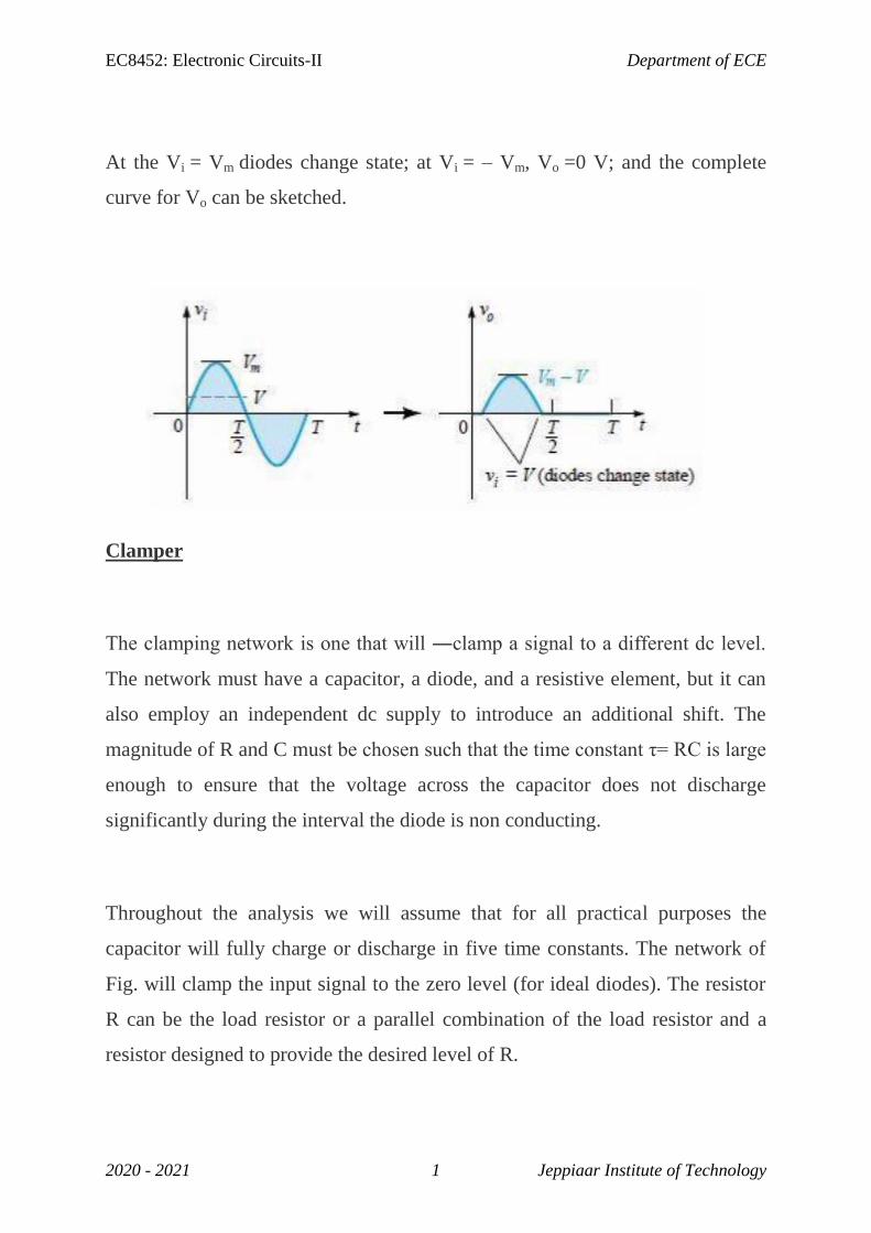
At the Vi = Vm diodes change state; at Vi = – Vm, Vo =0 V; and the complete
curve for Vo can be sketched.
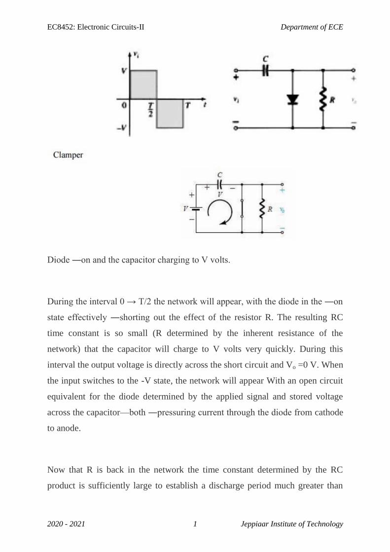
Clamper
The clamping network is one that will ―clamp a signal to a different dc level.
The network must have a capacitor, a diode, and a resistive element, but it can
also employ an independent dc supply to introduce an additional shift. The
magnitude of R and C must be chosen such that the time constant τ= RC is large
enough to ensure that the voltage across the capacitor does not discharge
significantly during the interval the diode is non conducting.
Throughout the analysis we will assume that for all practical purposes the
capacitor will fully charge or discharge in five time constants. The network of
Fig. will clamp the input signal to the zero level (for ideal diodes). The resistor
R can be the load resistor or a parallel combination of the load resistor and a
resistor designed to provide the desired level of R.
EC8452: Electronic Circuits-II Department of ECE
2020 - 2021 1 Jeppiaar Institute of Technology
Diode ―on and the capacitor charging to V volts.
During the interval 0 → T/2 the network will appear, with the diode in the ―on
state effectively ―shorting out the effect of the resistor R. The resulting RC
time constant is so small (R determined by the inherent resistance of the
network) that the capacitor will charge to V volts very quickly. During this
interval the output voltage is directly across the short circuit and Vo =0 V. When
the input switches to the -V state, the network will appear With an open circuit
equivalent for the diode determined by the applied signal and stored voltage
across the capacitor—both ―pressuring current through the diode from cathode
to anode.
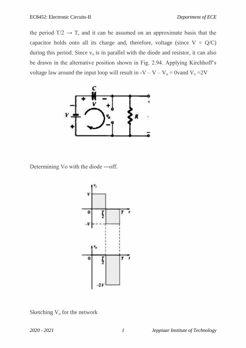
Now that R is back in the network the time constant determined by the RC
product is sufficiently large to establish a discharge period much greater than
EC8452: Electronic Circuits-II Department of ECE
2020 - 2021 1 Jeppiaar Institute of Technology
the period T/2 → T, and it can be assumed on an approximate basis that the
capacitor holds onto all its charge and, therefore, voltage (since V = Q/C)
during this period. Since vo is in parallel with the diode and resistor, it can also
be drawn in the alternative position shown in Fig. 2.94. Applying Kirchhoff‗s
voltage law around the input loop will result in -V – V – Vo = 0vand Vo =2V
Determining Vo with the diode ―off.
Sketching Vo for the network
EC8452: Electronic Circuits-II Department of ECE
2020 - 2021 1 Jeppiaar Institute of Technology
The negative sign resulting from the fact that the polarity of 2V is opposite to
the polarity defined for Vo. The resulting output waveform appears with the
input signal. The output signal is clamped to 0 V for the interval 0 to T/2 but
maintains the same total swing (2V) as the input. For a clamping network:
The total swing of the output is equal to the total swing of the input signal.
This fact is an excellent checking tool for the result obtained. In general, the
following steps may be helpful when analyzing clamping networks:
1. Start the analysis of clamping systems by considering that part of the input
signal that will forward bias the diode. The statement above may require
skipping an interval of the input signal (as demonstrated in an example to
follow), but the analysis will not be extended by an unnecessary measure of
investigation.
During the period that the diode is in the ―on state, assume that the capacitor
will charge up instantaneously to a voltage level determined by the network.
3. Assume that during the period when the diode is in the ―off state the
capacitor will hold on to its established voltage level.
4. Throughout the analysis maintain a continual awareness of the location and
reference polarity for to ensure that the proper levels for are obtained.
EC8452: Electronic Circuits-II Department of ECE
2020 - 2021 1 Jeppiaar Institute of Technology
5. Keep in mind the general rule that the total swing of the total output must
match the swing of the input signal .
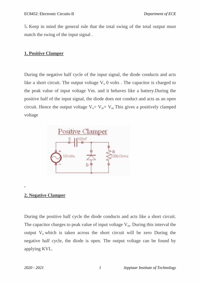
1. Positive Clamper
During the negative half cycle of the input signal, the diode conducts and acts
like a short circuit. The output voltage Vo 0 volts . The capacitor is charged to
the peak value of input voltage Vm. and it behaves like a battery.During the
positive half of the input signal, the diode does not conduct and acts as an open
circuit. Hence the output voltage Vo= Vm+ Vm This gives a positively clamped
voltage
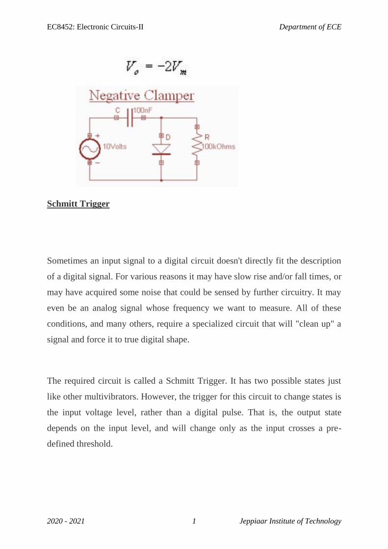
2. Negative Clamper
During the positive half cycle the diode conducts and acts like a short circuit.
The capacitor charges to peak value of input voltage Vm. During this interval the
output Vo which is taken across the short circuit will be zero During the
negative half cycle, the diode is open. The output voltage can be found by
applying KVL.
EC8452: Electronic Circuits-II Department of ECE
2020 - 2021 1 Jeppiaar Institute of Technology
Schmitt Trigger
Sometimes an input signal to a digital circuit doesn't directly fit the description
of a digital signal. For various reasons it may have slow rise and/or fall times, or
may have acquired some noise that could be sensed by further circuitry. It may
even be an analog signal whose frequency we want to measure. All of these
conditions, and many others, require a specialized circuit that will "clean up" a
signal and force it to true digital shape.
The required circuit is called a Schmitt Trigger. It has two possible states just
like other multivibrators. However, the trigger for this circuit to change states is
the input voltage level, rather than a digital pulse. That is, the output state
depends on the input level, and will change only as the input crosses a pre-
defined threshold.
EC8452: Electronic Circuits-II Department of ECE
2020 - 2021 1 Jeppiaar Institute of Technology
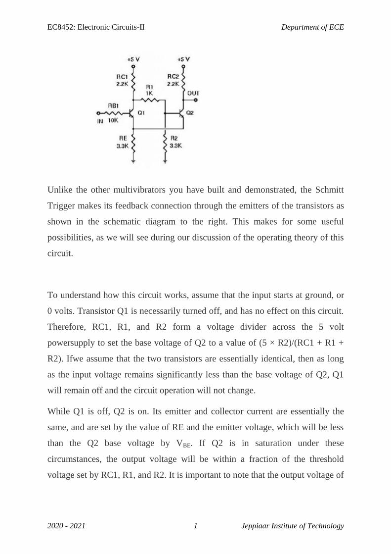
Unlike the other multivibrators you have built and demonstrated, the Schmitt
Trigger makes its feedback connection through the emitters of the transistors as
shown in the schematic diagram to the right. This makes for some useful
possibilities, as we will see during our discussion of the operating theory of this
circuit.
To understand how this circuit works, assume that the input starts at ground, or
0 volts. Transistor Q1 is necessarily turned off, and has no effect on this circuit.
Therefore, RC1, R1, and R2 form a voltage divider across the 5 volt
powersupply to set the base voltage of Q2 to a value of (5 × R2)/(RC1 + R1 +
R2). Ifwe assume that the two transistors are essentially identical, then as long
as the input voltage remains significantly less than the base voltage of Q2, Q1
will remain off and the circuit operation will not change.
While Q1 is off, Q2 is on. Its emitter and collector current are essentially the
same, and are set by the value of RE and the emitter voltage, which will be less
than the Q2 base voltage by VBE. If Q2 is in saturation under these
circumstances, the output voltage will be within a fraction of the threshold
voltage set by RC1, R1, and R2. It is important to note that the output voltage of
EC8452: Electronic Circuits-II Department of ECE
2020 - 2021 1 Jeppiaar Institute of Technology
this circuit cannot drop to zero volts, and generally not to a valid logic 0. We
can deal with that, but we must recognize this fact.
Now, suppose that the input voltage rises, and continues to rise until it
approaches the threshold voltage on Q2's base. At this point, Q1 begins to
conduct. Since it now carries some collector current, the current through RC1
increases and the voltage at the collector of Q1 decreases. But this also affects
our voltage divider, reducing the base voltage on Q2. But since Q1 is now
conducting it carries some of the current flowing through RE, and the voltage
across RE doesn't change as rapidly. Therefore, Q2 turns off and the output
voltage rises to +5 volts. The circuit has just changed states.
If the input voltage rises further, it will simply keep Q1 turned on and Q2 turned
off. However, if the input voltage starts to fall back towards zero, there must
clearly be a point at which this circuit will reset itself. The question is, What is
the falling threshold voltage? It will be the voltage at which Q1's base becomes
more negative than Q2's base, so that Q2 will begin conducting again. However,
it isn't the same as the rising threshold voltage, since Q1 is currently affecting
the behavior of the voltage divider.
We won't go through all of the derivation here, but when VIN becomes equal to
Q2's base voltage, Q2's base voltage will be:
As VIN approaches this value, Q2 begins to conduct, taking emitter current away
from Q1. This reduces the current through RC1 which raises Q2's base voltage
further, increasing Q2's forward bias and decreasing Q1's forward bias. This in
turn will turn off Q1, and the circuit will switch back to its original state.
EC8452: Electronic Circuits-II Department of ECE
2020 - 2021 1 Jeppiaar Institute of Technology
Three factors must be recognized in the Schmitt Trigger. First, the circuit will
change states as VINapproaches VB2, not when the two voltages are equal.
Therefore VB2 is very close to the threshold voltage, but is not precisely equal to
it. For example, for the component values shown above, VB2 will be 2.54 volts
when Q1 is held off, and 2.06 volts as VIN is falling towards this value.
Second, since the common emitter connection is part of the feedback system in
this circuit, RE must be large enough to provide the requisite amount of
feedback, without becoming so large as to starve the circuit of needed current. If
RE is out of range, the circuit will not operate properly, and may not operate as
anything more than a high-gain amplifier over a narrow input voltage range,
instead of switching states.
The third factor is the fact that the output voltage cannot switch over logic
levels, because the transistor emitters are not grounded. If a logic-level output is
required, which is usually the case, we can use a circuit such as the one shown
here to correct this problem. This circuit is basically two RTL inverters, except
that one uses a PNP transistor. This works because when Q2 above is turned off,
it will hold a PNP inverter off, but when it is on, its output will turn the PNP
transistor on. The NPN transistor here is a second inverter to re-invert the signal
and to restore it to active pull-down in common with all of our other logic
circuits.
The circuit you will construct for this experiment includes both of the circuits
shown here, so that you can monitor the response of the Schmitt trigger with L0.
EC8452: Electronic Circuits-II Department of ECE
2020 - 2021 1 Jeppiaar Institute of Technology
Schmitt Waveform Generators
Simple Waveform Generators can be constructed using basic Schmitt trigger
action Inverters such as the TTL 74LS14. This method is by far the easiest way
to make a basic astable waveform generator. When used to produce clock or
timing signals, the astable multivibrator must produce a stable waveform that
switches quickly between its "HIGH" and "LOW" states without any distortion
or noise, and Schmitt inverters do just that.
We know that the output state of a Schmitt inverter is the opposite or inverse to
that of its input state, (NOT Gate principles) and that it can change state at
different voltage levels giving it "hysteresis". Schmitt inverters use a Schmitt
Trigger action that changes state between an upper and a lower threshold level
as the input voltage signal increases and decreases about the input terminal.
This upper threshold level "sets" the output and the lower threshold
level"resets" the output which equates to a logic "0" and a logic "1" respectively
for an inverter. Consider the circuit below.
TTL Schmitt Waveform Generator
The circuit consists simply of a TTL 74LS14 Schmitt inverter logic gate with a
capacitor, C connected between its input terminal and ground, (0v) with the
positive feedback required for the circuit to oscillate is provided by the feedback
resistor, R. So how does it work?. Assume that the charge across the capacitors
plates is below the Schmitt's lower threshold level of 0.8 volt (Datasheet value).
EC8452: Electronic Circuits-II Department of ECE
2020 - 2021 1 Jeppiaar Institute of Technology
This therefore makes the input to the inverter at a logic "0" level resulting in a
logic "1" output level (inverter principals). One side of the resistor R is now
connected to the logic "1" level (+5V) output while the other side of the resistor
is connected to the capacitor, C which is at a logic "0" level (0.8v or below).
The capacitor now starts to charge up in a positive direction through the resistor
at a rate determined by the RC time constant of the combination. When the
charge across the capacitor reaches the 1.6 volt upper threshold level of the
Schmitt trigger (Datasheet value) the output from the Schmitt inverter changes
rapidly from a logic level "1" to a logic level "0" state and the current flowing
through the resistor changes direction.
This change now causes the capacitor that was originally charging up through
the resistor, R to begin to discharge itself back through the same resistor until
the charge across the capacitors plates reaches the lower threshold level of 0.8
volts and the inverters output switches state again with the cycle repeating itself
over and over again as long as the supply voltage is present.
So the capacitor, C is constantly charging and discharging itself during each
cycle between the upper and lower threshold levels of the Schmitt inverter
producing a logic level "1" or a logic level "0" at the inverters output. However,
the output square wave signal is not symmetrical producing a duty cycle of
about 33% or 1/3 as the mark-to-space ratio between "HIGH" and "LOW" is 1:2
respectively due to the input gate characteristics of the TTL inverter.
EC8452: Electronic Circuits-II Department of ECE
2020 - 2021 1 Jeppiaar Institute of Technology
The value of the feedback resistor, R MUST also be kept low to below 1kΩfor the
circuit to oscillate correctly, 220R to 470R is good, and by varying the value of the
capacitor, C to vary the frequency. Also at high frequency levels the output
waveform changes shape from a square shaped waveform to a trapezoidal
shaped waveform as the input characteristics of the TTL gate are affected by the
rapid charging and discharging of the capacitor.
With a resistor value between: 100R to 1kΩ, and a capacitor value of between:
1nF to 1000uF. This would give a frequency range of between 1Hzto 1MHz,
(high frequencies produce waveform distortion).
Waveform Generator
Nonsinusoidal oscillators generate complex waveforms such as those just
discussed. Because the outputs of these oscillators are generally characterized
by a sudden change, or relaxation, these oscillators are often called
RELAXATION OSCILLATORS. The pulse repetition rate of these oscillators
is usually governed by the charge and discharge timing of a capacitor in series
with a resistor.
However, some oscillators contain inductors that along with circuit resistance,
affect the output frequency. These RC and LC networks within oscillator
circuits are used for frequency determination. Within this category of relaxation
oscillators are MULTIVIBRATORS,BLOCKING OSCILLATORS, and
SAWTOOTH- and TRAPEZOIDAL-WAVE GENERATORS. Many electronic
circuits are not in an "on" condition all of the time. In computers, for example,
waveforms must be turned on and off for specific lengths of time.
EC8452: Electronic Circuits-II Department of ECE
2020 - 2021 1 Jeppiaar Institute of Technology
The time intervals vary from tenths of microseconds to several thousand
microseconds. Square and rectangular waveforms are normally used to turn
such circuits on and off because the sharp leading and trailing edges make them
ideal for timing purposes.
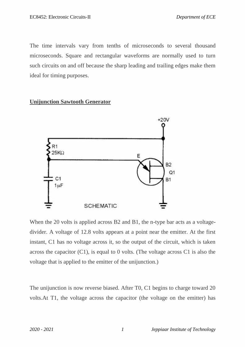
Unijunction Sawtooth Generator
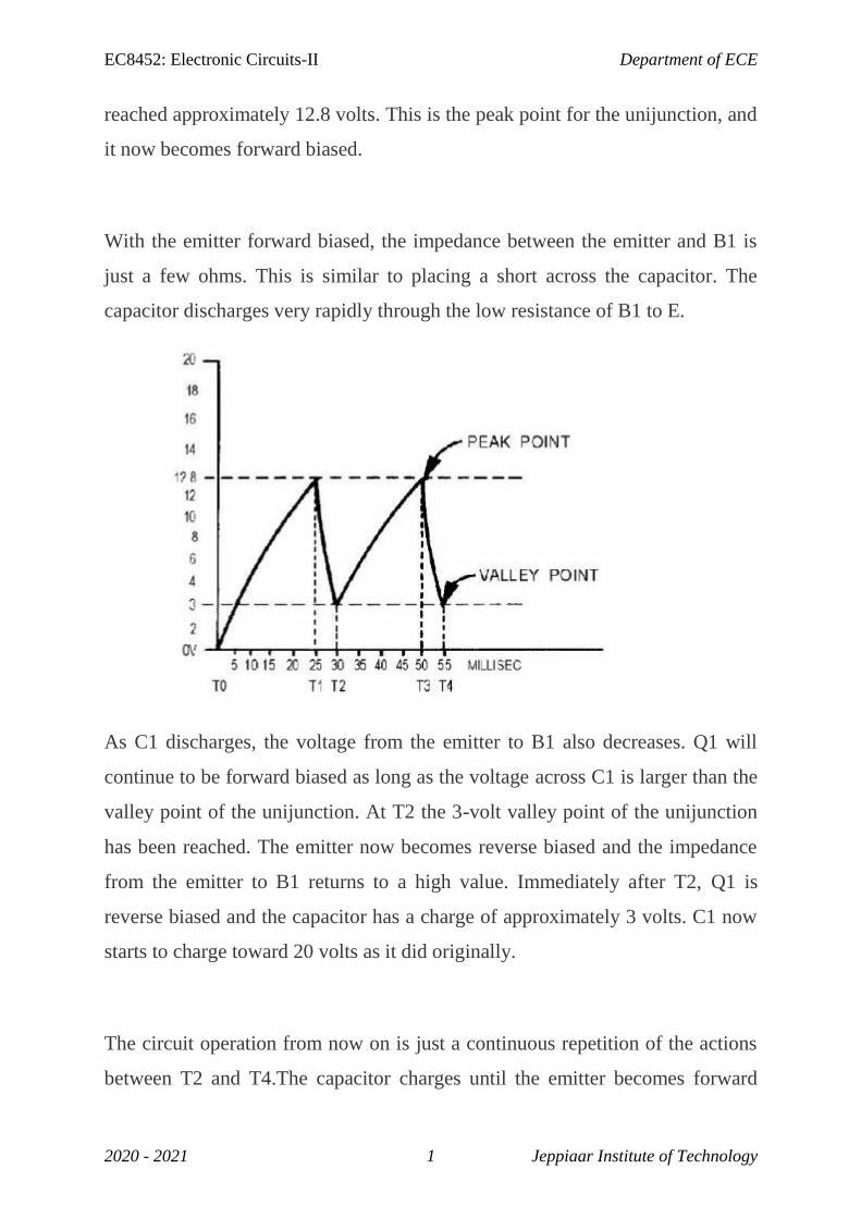
When the 20 volts is applied across B2 and B1, the n-type bar acts as a voltage-
divider. A voltage of 12.8 volts appears at a point near the emitter. At the first
instant, C1 has no voltage across it, so the output of the circuit, which is taken
across the capacitor (C1), is equal to 0 volts. (The voltage across C1 is also the
voltage that is applied to the emitter of the unijunction.)
The unijunction is now reverse biased. After T0, C1 begins to charge toward 20
volts.At T1, the voltage across the capacitor (the voltage on the emitter) has
EC8452: Electronic Circuits-II Department of ECE
2020 - 2021 1 Jeppiaar Institute of Technology
reached approximately 12.8 volts. This is the peak point for the unijunction, and
it now becomes forward biased.
With the emitter forward biased, the impedance between the emitter and B1 is
just a few ohms. This is similar to placing a short across the capacitor. The
capacitor discharges very rapidly through the low resistance of B1 to E.
As C1 discharges, the voltage from the emitter to B1 also decreases. Q1 will
continue to be forward biased as long as the voltage across C1 is larger than the
valley point of the unijunction. At T2 the 3-volt valley point of the unijunction
has been reached. The emitter now becomes reverse biased and the impedance
from the emitter to B1 returns to a high value. Immediately after T2, Q1 is
reverse biased and the capacitor has a charge of approximately 3 volts. C1 now
starts to charge toward 20 volts as it did originally.
The circuit operation from now on is just a continuous repetition of the actions
between T2 and T4.The capacitor charges until the emitter becomes forward
EC8452: Electronic Circuits-II Department of ECE
2020 - 2021 1 Jeppiaar Institute of Technology
biased, the unijunction conducts and C1discharges, and Q1 becomes reverse
biased and C1 again starts charging.
Now, let's determine the linearity, electrical length, and amplitude of the output
waveform. First, the linearity: To charge the circuit to the full 20 volts will take
5 time constants. In the circuit shown in figure 3-44, view (B), C1 is allowed to
charge from T2 to T3. To find the percentage of charge, use the equation:
This works out to be about 57 percent and is far beyond the 10 percent required
for a linear sweep voltage.
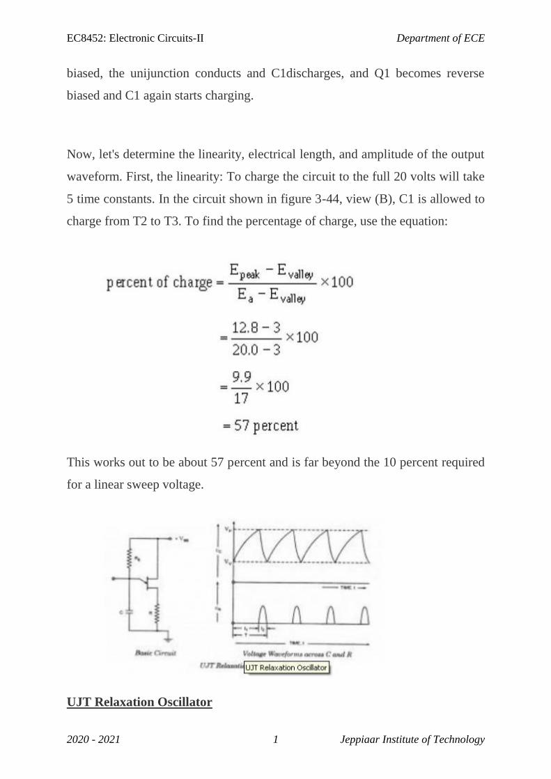
UJT Relaxation Oscillator
EC8452: Electronic Circuits-II Department of ECE
2020 - 2021 1 Jeppiaar Institute of Technology
The relaxation oscillator shown in figure consists of UJT and a capacitor C
which is charged through resistor RE when inter base voltage VBB is switched
on. During the charging period, the voltage across the capacitor increases
exponentially until it attains the peak point voltage VP.
When the capacitor voltage attains voltage VP, the UJT switches on and the
capacitor C rapidly discharges through B1. The resulting current through the
external resistor R develops a voltage spike, as illustrated in figure and the
capacitor voltage drops to the value VV.
The device then cuts off and the capacitor commences charging again. The
cycle is repeated continually generating a saw-tooth waveform across
capacitor C. The resulting waveforms of capacitor voltage VC and the voltage
across resistor R (VR) are shown in figure. The frequency of the input saw-
tooth wave can be varied by varying the value of resistor RE as it controls the
time constant (T = REC) of the capacitor charging circuit.
The discharge time t2 is difficult to calculate because the UJT is in its negative
resistance region and its resistance is continually changing. However, t2 is
normally very much less than t1 and can be neglected for approximation.
For satisfactory operation of the above oscillator the following two conditions
for the turn-on and turn-off of the UJT must be met.
EC8452: Electronic Circuits-II Department of ECE
2020 - 2021 1 Jeppiaar Institute of Technology
RE < VBB – VP / IP and RE > VBB – VV / IV
That is the range of resistor RE should be as given below
VBB – VP / IP > RE > VBB – VV / IV
The time period and, therefore, frequency of oscillation can be derived as
below. During charging of capacitor, the voltage across the capacitor is given as
Vc = VBB(l-e-/ReC
)
where REC is the time constant of the capacitor charging circuit and t is the time
from the commencement of the charging.The discharge of the capacitor
commences at the end of charging period t1 when the voltage across the
capacitor Vc becomes equal to VP, that is, (ȠVBB + VB)
VP = ȠVBB + VB = VBB(l-e-/ReC
) Neglecting VB in comparison to ȠVBB we have
ȠVBB = VBB(l-e-1/ReC
)
Or e-t1/ReC
= 1 – Ƞ
So charging time period, t1 = 2.3 RE C log10 1/1- Ƞ
EC8452: Electronic Circuits-II Department of ECE
2020 - 2021 1 Jeppiaar Institute of Technology
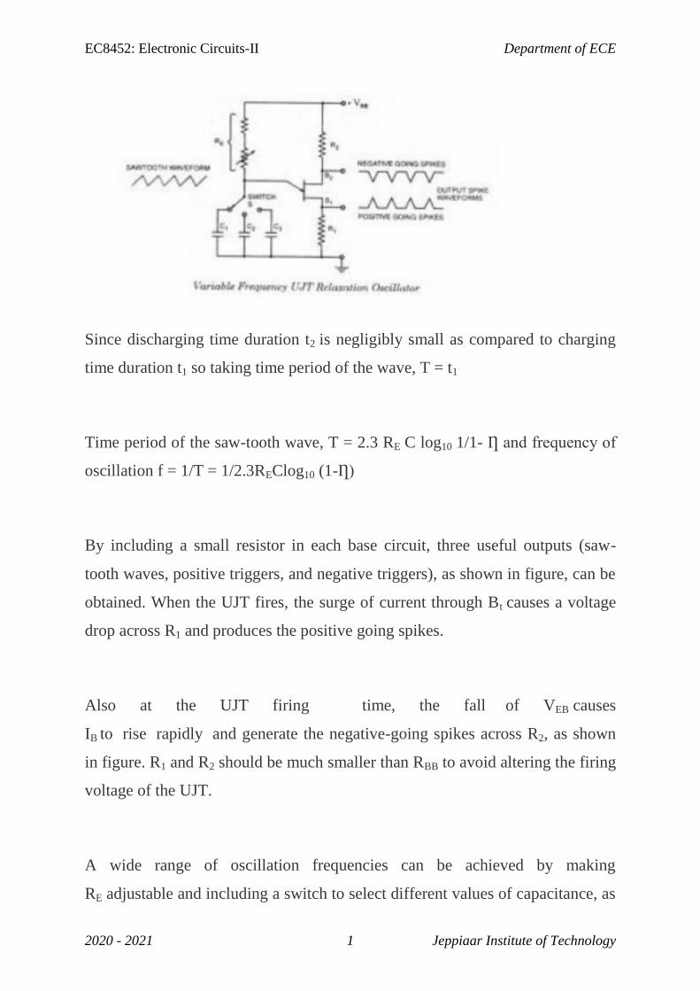
Since discharging time duration t2 is negligibly small as compared to charging
time duration t1 so taking time period of the wave, T = t1
Time period of the saw-tooth wave, T = 2.3 RE C log10 1/1- Ƞ and frequency of
oscillation f = 1/T = 1/2.3REClog10 (1-Ƞ)
By including a small resistor in each base circuit, three useful outputs (saw-
tooth waves, positive triggers, and negative triggers), as shown in figure, can be
obtained. When the UJT fires, the surge of current through Bt causes a voltage
drop across R1 and produces the positive going spikes.
Also at the UJT firing time, the fall of VEB causes
IB to rise rapidly and generate the negative-going spikes across R2, as shown
in figure. R1 and R2 should be much smaller than RBB to avoid altering the firing
voltage of the UJT.
A wide range of oscillation frequencies can be achieved by making
RE adjustable and including a switch to select different values of capacitance, as
EC8452: Electronic Circuits-II Department of ECE
2020 - 2021 1 Jeppiaar Institute of Technology
illustrated. As already mentioned in previous blog post there is upper and lower
limits to the signal source resistance RE for the satisfactory operation of the
UJT.
Pulse Transformer
A pulse transformer is a transformer that is optimised for transmitting
rectangular electrical pulses (that is, pulses with fast rise and fall times and a
relatively constant amplitude). Small versions called signal types are used in
digital logic and telecommunications circuits, often for matching logic drivers
to transmission lines. Medium-sized power versions are used in power-control
circuits such as camera flash controllers. Larger power versions are used in the
electrical power distribution industry to interface low-voltage control circuitry
to the high-voltage gates of power semiconductors. Special high voltage pulse
transformers are also used to generate high power pulses for radar, particle
accelerators, or other high energy pulsed power applications.
To minimise distortion of the pulse shape, a pulse transformer needs to have
low values of leakage inductance and distributed capacitance, and a highopen-
circuit inductance. In power-type pulse transformers, a low coupling
capacitance (between the primary and secondary) is important to protect the
circuitry on the primary side from high-powered transients created by the load.
For the same reason, high insulation resistance and high breakdown voltage are
required. A good transient response is necessary to maintain the rectangular
pulse shape at the secondary, because a pulse with slow edges would create
switching losses in the power semiconductors.
EC8452: Electronic Circuits-II Department of ECE
2020 - 2021 1 Jeppiaar Institute of Technology
The product of the peak pulse voltage and the duration of the pulse (or more
accurately, the voltage-time integral) is often used to characterise pulse
transformers. Generally speaking, the larger this product, the larger and more
expensive the transformer.
Pulse transformers by definition have a duty cycle of less than 0.5, whatever
energy stored in the coil during the pulse must be "dumped" out before the pulse
is fired again.