Background noise and noise levels from en-route Aircraft ...
Upload
khangminh22Category
view
0download
0
Outp
ut S
pectr
al N
ois
e D
ensity (
V/
)m
Hz
Ö
100 1 k 10 k 100 k
Frequency (Hz)
0.7
0.6
0.5
0.4
0.3
0.2
0.1
0
I = 1.5 AOUT
I = 1 AOUT
V = 5.5 VIN
C = 2.2 F
C = 0.1 FOUT
NR
m
m
80
70
60
50
40
30
20
10
0
Rip
ple
Reje
ction (
dB
)
1 10 100 1 k 10 k 100 k 1 M 10 M
Frequency (Hz)
I = 1 mAOUT
I = 1 AOUT
V = 4 VIN
C = 10 F
C = 0.01 FOUT
NR
m
m
Product
Folder
Sample &Buy
Technical
Documents
Tools &
Software
Support &Community
TPS79601, TPS79613, TPS79618, TPS79625TPS79628, TPS79630, TPS79633, TPS79650
SLVS351P –SEPTEMBER 2002–REVISED MARCH 2015
TPS796xx Ultralow-Noise, High PSRR, Fast, RF, 1-A Low-Dropout Linear Regulators1 Features 3 Description
The TPS796 family of low-dropout (LDO) low-power1• 1-A Low-Dropout Regulator With Enable
linear voltage regulators features high power-supply• Available in Fixed and Adjustable (1.2 V to 5.5 V) rejection ratio (PSRR), ultralow-noise, fast start-up,Versions and excellent line and load transient responses in
• High PSRR (53 dB at 10 kHz) small outline, 3 × 3 VSON, SOT223-6, and TO-263packages. Each device in the family is stable with a• Ultralow-Noise (40 μVRMS, TPS79630)small, 1-μF ceramic capacitor on the output. The• Fast Start-Up Time (50 μs) family uses an advanced, proprietary BiCMOS
• Stable With a 1-μF Ceramic Capacitor fabrication process to yield extremely low dropoutvoltages (for example, 250 mV at 1 A). Each device• Excellent Load and Line Transient Responseachieves fast start-up times (approximately 50 μs with• Very Low Dropout Voltage (250 mV at Full Load, a 0.001-μF bypass capacitor) while consuming veryTPS79630) low quiescent current (265 μA typical). Moreover,
• 3 × 3 VSON PowerPAD™, SOT223-6, and when the device is placed in standby mode, theTO-263 Packages supply current is reduced to less than 1 μA. The
TPS79630 exhibits approximately 40 μVRMS of outputvoltage noise at 3.0-V output, with a 0.1-μF bypass2 Applicationscapacitor. Applications with analog components that• RF: VCOs, Receivers, ADCs are noise sensitive, such as portable RF electronics,
• Audio benefit from the high PSRR, low noise features, andneed fast response time.• Bluetooth®, Wireless LAN
• Cellular and Cordless Telephones Device Information(1)• Handheld Organizers, PDAs
PART NUMBER PACKAGE BODY SIZE (NOM)VSON (8) 3.00 mm × 3.00 mm
TPS796 SOT-223 (6) 6.50 mm × 3.50 mmTO-263 (5) 10.16 mm × 8.42 mm
(1) For all available packages, see the orderable addendum atthe end of the data sheet.
Ripple Rejection vs FrequencyOutput Spectral Noise Density vs FrequencyTPS79630
TPS79630
1
An IMPORTANT NOTICE at the end of this data sheet addresses availability, warranty, changes, use in safety-critical applications,intellectual property matters and other important disclaimers. PRODUCTION DATA.

TPS79601, TPS79613, TPS79618, TPS79625TPS79628, TPS79630, TPS79633, TPS79650SLVS351P –SEPTEMBER 2002–REVISED MARCH 2015 www.ti.com
Table of Contents8.1 Application Information............................................ 141 Features .................................................................. 18.2 Typical Application .................................................. 142 Applications ........................................................... 18.3 Do's and Don'ts ...................................................... 173 Description ............................................................. 1
9 Power Supply Recommendations ...................... 174 Revision History..................................................... 210 Layout................................................................... 175 Pin Configuration and Functions ......................... 3
10.1 Layout Guidelines ................................................. 176 Specifications......................................................... 410.2 Layout Examples................................................... 186.1 Absolute Maximum Ratings ...................................... 410.3 Thermal Considerations ........................................ 196.2 ESD Ratings ............................................................ 410.4 Estimating Junction Temperature ........................ 206.3 Recommended Operating Conditions....................... 4
11 Device and Documentation Support ................. 226.4 Thermal Information .................................................. 511.1 Device Support...................................................... 226.5 Electrical Characteristics........................................... 611.2 Documentation Support ........................................ 226.6 Typical Characteristics .............................................. 711.3 Related Links ........................................................ 227 Detailed Description ............................................ 1111.4 Trademarks ........................................................... 237.1 Overview ................................................................. 1111.5 Electrostatic Discharge Caution............................ 237.2 Functional Block Diagrams ..................................... 1111.6 Glossary ................................................................ 237.3 Feature Description................................................. 12
12 Mechanical, Packaging, and Orderable7.4 Device Functional Modes........................................ 13Information ........................................................... 238 Application and Implementation ........................ 14
4 Revision HistoryNOTE: Page numbers for previous revisions may differ from page numbers in the current version.
Changes from Revision O (November 2013) to Revision P Page
• Added ESD Ratings table, Feature Description section, Device Functional Modes, Application and Implementationsection, Power Supply Recommendations section, Layout section, Device and Documentation Support section, andMechanical, Packaging, and Orderable Information section ................................................................................................. 1
• Changed front-page figure; updated graph style, replaced device pinouts with application circuits ..................................... 1• Changed Pin Configuration and Functions section; updated table format and added pinout drawings................................. 3• Changed "free-air" to "junction" temperature in condition statement for Absolute Maximum Ratings .................................. 4• Changed VOUT accuracy for TPS79601, test conditions and specified values ...................................................................... 6• Deleted Start-up time symbol ................................................................................................................................................. 6• Added Thermal shutdown temperature specification to Electrical Characteristics ................................................................ 6• Added Operating junction temperature specification to Electrical Characteristics ................................................................ 6• Added condition statement to Typical Characteristics ........................................................................................................... 7
Changes from Revision N (January 2011) to Revision O Page
• Changed Power-Supply Ripple Rejection 3rd test condition from "f = 10 Hz" to "f = 10 kHz" (typo) .................................... 6• Changed Power-Supply Ripple Rejection 4th test condition from "f = 100 Hz" to "f = 100 kHz" (typo) ................................ 6
Changes from Revision M (October 2010) to Revision N Page
• Corrected typo in front-page figure......................................................................................................................................... 1
Changes from Revision L (August 2010) to Revision M Page
• Corrected typo in Figure 32 ................................................................................................................................................. 21
2 Submit Documentation Feedback Copyright © 2002–2015, Texas Instruments Incorporated
Product Folder Links: TPS79601 TPS79613 TPS79618 TPS79625 TPS79628 TPS79630 TPS79633 TPS79650

3
4 5
6
7
8
2
1IN
OUT
IN N/C
GND
OUT NR/FB
EN
IN OUT
GND NR/FBEN
1 2 3 4
6
5
IN
OUT
GND
NR/FB
EN 1
2
3
4
5
TPS79601, TPS79613, TPS79618, TPS79625TPS79628, TPS79630, TPS79633, TPS79650
www.ti.com SLVS351P –SEPTEMBER 2002–REVISED MARCH 2015
5 Pin Configuration and Functions
DCQ PackageKTT Package6-Pin SOT-2235-Pin TO-263Top View
Top View
DRB Package8-Pin VSON
Top View
Pin FunctionsPIN
I/O DESCRIPTIONSOT223NAME VSONTO-263Driving the enable pin (EN) high turns on the regulator. Driving this pin low puts theEN 1 8 I regulator into shutdown mode. EN can be connected to IN if not used.
FB 5 5 I This terminal is the feedback input voltage for the adjustable device.6, Regulator groundGND 3, Tab —PowerPAD
IN 2 1, 2 I Unregulated input to the device.N/C — 7 — Not internally connected. This pin must either be left open, or tied to GND.
Connecting an external capacitor to this pin bypasses noise generated by theNR 5 5 — internal bandgap. This improves power-supply rejection and reduces output noise.OUT 4 3, 4 O Output of the regulator.
Copyright © 2002–2015, Texas Instruments Incorporated Submit Documentation Feedback 3
Product Folder Links: TPS79601 TPS79613 TPS79618 TPS79625 TPS79628 TPS79630 TPS79633 TPS79650

TPS79601, TPS79613, TPS79618, TPS79625TPS79628, TPS79630, TPS79633, TPS79650SLVS351P –SEPTEMBER 2002–REVISED MARCH 2015 www.ti.com
6 Specifications
6.1 Absolute Maximum Ratingsover operating junction temperature range (unless otherwise noted) (1)
MIN MAX UNITIN –0.3 6
Voltage EN –0.3 VIN + 0.3 VOUT 6
Current Peak output Internally limitedPower dissipation Continuous total See Thermal Information
Junction, TJ –40 150Temperature °C
Storage, Tstg –65 150
(1) Stresses beyond those listed under Absolute Maximum Ratings may cause permanent damage to the device. These are stress ratingsonly, which do not imply functional operation of the device at these or any other conditions beyond those indicated under RecommendedOperating Conditions. Exposure to absolute-maximum-rated conditions for extended periods may affect device reliability.
6.2 ESD RatingsVALUE UNIT
Human body model (HBM), per ANSI/ESDA/JEDEC JS-001, all pins (1) ±2000V(ESD) Electrostatic discharge VCharged device model (CDM), per JEDEC specification JESD22-C101, ±500all pins (2)
(1) JEDEC document JEP155 states that 500-V HBM allows safe manufacturing with a standard ESD control process.(2) JEDEC document JEP157 states that 250-V CDM allows safe manufacturing with a standard ESD control process.
6.3 Recommended Operating Conditionsover operating junction temperature range (unless otherwise noted)
MIN NOM MAX UNITVIN Input voltage 2.7 5.5 VIOUT Output current 0 1 ATJ Operating junction temperature –40 125 °C
4 Submit Documentation Feedback Copyright © 2002–2015, Texas Instruments Incorporated
Product Folder Links: TPS79601 TPS79613 TPS79618 TPS79625 TPS79628 TPS79630 TPS79633 TPS79650

TPS79601, TPS79613, TPS79618, TPS79625TPS79628, TPS79630, TPS79633, TPS79650
www.ti.com SLVS351P –SEPTEMBER 2002–REVISED MARCH 2015
6.4 Thermal InformationTPS796xx (3)
DRB (VSON) DCQ KTT (TO-263)THERMAL METRIC (1) (2) UNIT(SOT-223)8 PINS 6 PINS 5 PINS
RθJA Junction-to-ambient thermal resistance 47.8 70.4 25RθJC(top) Junction-to-case (top) thermal resistance 83 70 35RθJB Junction-to-board thermal resistance N/A N/A N/A
°C/WψJT Junction-to-top characterization parameter 2.1 6.8 1.5ψJB Junction-to-board characterization parameter 17.8 30.1 8.52RθJC(bot) Junction-to-case (bottom) thermal resistance 12.1 6.3 0.4
(1) For more information about traditional and new thermal metrics, see the IC Package Thermal Metrics application report, SPRA953.(2) For thermal estimates of this device based on PCB copper area, see the TI PCB Thermal Calculator.(3) Thermal data for the DRB, DCQ, and DRV packages are derived by thermal simulations based on JEDEC-standard methodology as
specified in the JESD51 series. The following assumptions are used in the simulations:(a) i. DRB: The exposed pad is connected to the PCB ground layer through a 2 × 2 thermal via array.
. ii. DCQ: The exposed pad is connected to the PCB ground layer through a 3 × 2 thermal via array.
. iii. KTT: The exposed pad is connected to the PCB ground layer through a 5 × 4 thermal via array.(b) i. DRB: The top and bottom copper layers are assumed to have a 20% thermal conductivity of copper representing a 20% copper
coverage.. ii. DCQ: Each of top and bottom copper layers has a dedicated pattern for 20% copper coverage.. iii. KTT: The top and bottom copper layers are assumed to have a 20% thermal conductivity of copper representing a 20% coppercoverage.
(c) These data were generated with only a single device at the center of a JEDEC high-K (2s2p) board with 3in × 3in copper area. Tounderstand the effects of the copper area on thermal performance, see Power Dissipation and Estimating Junction Temperature.
Copyright © 2002–2015, Texas Instruments Incorporated Submit Documentation Feedback 5
Product Folder Links: TPS79601 TPS79613 TPS79618 TPS79625 TPS79628 TPS79630 TPS79633 TPS79650

TPS79601, TPS79613, TPS79618, TPS79625TPS79628, TPS79630, TPS79633, TPS79650SLVS351P –SEPTEMBER 2002–REVISED MARCH 2015 www.ti.com
6.5 Electrical CharacteristicsOver recommended operating temperature range (TJ = –40°C to 125°C), VEN = VIN,, VIN = VOUT(nom) + 1 V (1), IOUT = 1 mA, COUT= 10 μF, and CNR = 0.01 μF, unless otherwise noted. Typical values are at 25°C.
PARAMETER TEST CONDITIONS MIN TYP MAX UNIT
VIN Input voltage (1) 2.7 5.5 V
VFB Internal reference (TPS79601) 1.2 1.225 1.25 V
IOUT Continuous output current 0 1 A
Output voltage TPS79601 1.225 5.5 – VDO Vrange
TPS79601 (2) 0 μA ≤ IOUT ≤ 1 A, VOUT(nom) + 1 V ≤ VIN ≤ 5.5 V (1) 0.98VOUT(nom) VOUT(nom) 1.02VOUT(nom) VVOUT
Accuracy Fixed VOUT < 5 V 0 μA ≤ IOUT ≤ 1 A, VOUT(nom) + 1 V ≤ VIN ≤ 5.5 V (1) –2% 2%
Fixed VOUT = 5 V 0 μA ≤ IOUT ≤ 1 A, VOUT(nom) + 1 V ≤ VIN ≤ 5.5 V (1) –3% 3%
ΔVO(ΔVI) Line regulation (1) VOUT + 1 V ≤ VIN ≤ 5.5 V 0.05 0.12 %/V
ΔVO(ΔIO) Load regulation 0 μA ≤ IOUT ≤ 1 A 5 mV
TPS79628 IOUT = 1 A 270 365
TPS79628DRB IOUT = 250 mA 52 90Dropout voltage (3)
VDO (VIN = VOUT(nom) – TPS79630 IOUT = 1 A 250 345 mV0.1 V) TPS79633 IOUT = 1 A 220 325
TPS79650 IOUT = 1 A 200 300
ICL Output current limit VOUT = 0 V 2.4 4.2 A
IGND Ground pin current 0 μA ≤ IOUT ≤ 1 A 265 385 μA
ISHDN Shutdown current (4) VEN = 0 V, 2.7 V ≤ VIN ≤ 5.5 V 0.07 1 μA
IFB Feedback pin current VFB = 1.225 V 1 µA
f = 100 Hz. IOUT = 10 mA 59
f = 100 Hz, IOUT = 1 A 54Power-supply rejection ratioPSRR dB(TPS79630) f = 10 kHz, IOUT = 1A 53
f = 100 kHz, IOUT = 1 A 42
CNR = 0.001 μF 54
CNR = 0.0047 μF 46BW = 100 Hz to 100 kHz,Vn Output noise voltage (TPS79630) μVRMSIOUT = 1 A CNR = 0.01 μF 41
CNR = 0.1 μF 40
CNR = 0.001 μF 50RL = 3 Ω,Start-up time (TPS79630) CNR = 0.0047 μF 75 μsCOUT = 1 μF
CNR = 0.01 μF 110
VEN(HI) Enable high (enabled) 2.7 V ≤ VIN ≤ 5.5 V 1.7 VIN V
VEN(LO) Enable low (shutdown) 2.7 V ≤ VIN ≤ 5.5 V 0 0.7 V
IEN(HI) Enable pin current, enabled VEN = 0 V –1 1 μA
Undervoltage lockout VCC rising 2.25 2.65 VUVLO
Hysteresis 100 mV
Shutdown, temperature increasing 165Tsd Thermal shutdown temperature °C
Reset, temperature decreasing 140
TJ Operating junction temperature –40 125 °C
(1) Minimum VIN = VOUT + VDO or 2.7 V, whichever is greater. TPS79650 is tested at VIN = 5.5 V.(2) Tolerance of external resistors not included in this specification.(3) VDO is not measured for TPS79618 and TPS79625 because minimum VIN = 2.7 V.(4) For adjustable version, this applies only after VIN is applied; then VEN transitions high to low.
6 Submit Documentation Feedback Copyright © 2002–2015, Texas Instruments Incorporated
Product Folder Links: TPS79601 TPS79613 TPS79618 TPS79625 TPS79628 TPS79630 TPS79633 TPS79650

0.0
0.1
0.2
0.3
0.4
0.5
0.6
Frequency (Hz)
100 10k 100k1k
Ou
tpu
t S
pectr
al N
ois
e D
en
sit
y−
mV
/ÖH
z
IOUT = 1 mA
IOUT = 1 A
VIN = 5.5 V
COUT = 10 FmCNR = 0.1 Fm
0.0
0.5
1.0
1.5
2.0
2.5
Frequency (Hz)
100 10k 100k1k
VIN = 5.5 V
COUT = 10 FmIOUT = 1 A
CNR = 0.1 Fm
CNR = 0.01 Fm
CNR = 0.0047 Fm
CNR = 0.001 Fm
Ou
tpu
t S
pectr
al N
ois
e D
en
sit
y−
mV
/ÖH
z
290
300
310
320
330
340
350
−40 −25 −10 5 20 35 50 65 80 95 110 125
I GN
D(m
A)
TJ (°C)
VIN = 3.8 V
COUT = 10 Fm
IOUT = 1 mA
IOUT = 1 A
0.0
0.1
0.2
0.3
0.4
0.5
0.6
0.7
Frequency (Hz)
100 10k 100k1k
IOUT = 1 mA
IOUT = 1.5 A
VIN = 5.5 V
COUT = 2.2 FmCNR = 0.1 Fm
Ou
tpu
t S
pectr
al
No
ise
Den
sit
y−
mV
/ÖH
z
2.95
2.96
2.97
2.98
2.99
3.00
3.01
3.02
3.03
3.04
3.05
0.0 0.2 0.4 0.6 0.8 1.0
VO
UT
(V)
IOUT (A)
VIN = 4 V
COUT = 10 Fm
TJ = 25 C°
0
1
2
3
4
−40 −25 −10 5 20 35 50 65 80 95 110 125
VO
UT
(V)
TJ ( C)°
IOUT = 1 mA
2.795
2.790
2.785
2.780
2.775
IOUT = 1 A
VIN = 3.8 V
COUT = 10 Fm
TPS79601, TPS79613, TPS79618, TPS79625TPS79628, TPS79630, TPS79633, TPS79650
www.ti.com SLVS351P –SEPTEMBER 2002–REVISED MARCH 2015
6.6 Typical CharacteristicsAt VEN = VIN, VIN = VOUT(nom) + 1 V, IOUT = 1 mA, COUT = 10 µF, CNR = 0.01 µF, CIN = 2.2 µF, and TJ = 25°C, unless otherwisenoted.
Figure 1. TPS79630 Output Voltage vs Output Current Figure 2. TPS79628 Output Voltage vsJunction Temperature
Figure 3. TPS79628 Ground Current vs Figure 4. TPS79630 Output Spectral Noise Density vsFrequencyJunction Temperature
Figure 5. TPS79630 Output Spectral Noise Density vs Figure 6. TPS79630 Output Spectral Noise Density vsFrequency Frequency
Copyright © 2002–2015, Texas Instruments Incorporated Submit Documentation Feedback 7
Product Folder Links: TPS79601 TPS79613 TPS79618 TPS79625 TPS79628 TPS79630 TPS79633 TPS79650

0
10
20
30
40
50
60
70
80
Frequency (Hz)
1 10k 10M1k
Rip
ple
Reje
cti
on
−d
B
IOUT = 1 mA
IOUT = 1 A
VIN = 4 V
COUT = 2.2 Fm
CNR = 0.01 Fm
10 100 100k 1M
0
0.25
0.50
0.75
1
1.25
1.50
1.75
2
2.25
2.50
2.75
3
0 100 200 300 400 500 600
t (µs)
VIN = 4 V,
COUT = 10 F,m
IOUT = 1.0 A
Enable
CNR =
0.01 Fm
CNR =
0.001 Fm
CNR =
0.0047 Fm
VO
UT
(V)
0
10
20
30
40
50
60
70
80
Frequency (Hz)
1 10k 10M1k
Rip
ple
Reje
cti
on
−d
B
IOUT = 1 mA
IOUT = 1 A
VIN = 4 V
COUT = 10 Fm
CNR = 0.01 Fm
10 100 100k 1M
0
10
20
30
40
50
60
70
80
Frequency (Hz)
1 10k 10M1k
Rip
ple
Reje
cti
on
−d
B
IOUT = 1 mA
IOUT = 1 A
VIN = 4 V
COUT = 10 Fm
CNR = 0.1 Fm
10 100 100k 1M
0
10
20
30
40
50
60
RM
S−
Ro
ot
Mean
Sq
uare
d O
utp
ut
No
ise
−m
VR
MS
CNR (mF)
IOUT = 250 mA
COUT = 10 Fm
0.001 Fm 0.01 Fm 0.1 Fm0.0047 Fm
BW = 100 Hz to 100 kHz
0
50
100
150
200
250
300
350
- - -40 25 10 5 20 35 50 65 80 95 110 125
VD
O(m
V)
TJ
(°C)
VIN
= 2.7 V
COUT
= 10 mF
IOUT
= 1 A
IOUT
= 250 mA
TPS79601, TPS79613, TPS79618, TPS79625TPS79628, TPS79630, TPS79633, TPS79650SLVS351P –SEPTEMBER 2002–REVISED MARCH 2015 www.ti.com
Typical Characteristics (continued)At VEN = VIN, VIN = VOUT(nom) + 1 V, IOUT = 1 mA, COUT = 10 µF, CNR = 0.01 µF, CIN = 2.2 µF, and TJ = 25°C, unless otherwisenoted.
Figure 8. TPS79628 Dropout Voltage vsFigure 7. TPS79630 Root Mean Squared Output Noise vsJunction TemperatureBypass Capacitance
Figure 9. TPS79630 Ripple Rejection vs Frequency Figure 10. TPS79630 Ripple Rejection vs Frequency
Figure 11. TPS79630 Ripple Rejection vs Frequency Figure 12. Start-Up Time
8 Submit Documentation Feedback Copyright © 2002–2015, Texas Instruments Incorporated
Product Folder Links: TPS79601 TPS79613 TPS79618 TPS79625 TPS79628 TPS79630 TPS79633 TPS79650

0
50
100
150
200
250
300
2.5 3.0 3.5 4.0 4.5 5.0
VD
O(m
V)
VIN (V)
TJ = 125°C
TJ = −40°C
TJ = 25°C
IOUT = 1 A
COUT = 10 µF
CNR = 0.01 µF
0
50
100
150
200
250
300
350
0 100 200 300 400 500 600 700 800 9001000
VD
O(m
V)
IOUT (mA)
TJ = 125°C
TJ = −40°C
TJ = 25°C
t (ms)
2
1
−1
−75
−150
0
0
75
150
3002001000 400 500 600 700 800 900 1000
VIN = 3.8 V
COUT = 10 Fm
CNR = 0.01 Fm
di
dt
1 Aµs
I OU
T(A
)D
VO
UT
(mV
)
200 s/Divm
4.0
3.5
2.5
0.5
0
3.0
1.0
1.5
2.0500
mV
/Div
3210 4 5 6 7 8 9 10
VOUT = 2.5 V
RL = 10 W
CNR = 0.01 Fm
VIN
VOUT
0
20
VIN
(V)
t (ms)
5
4
2
−20
−40
3
40
6040200 80 100 120 140 160 180 200
IOUT = 1 A
COUT = 10 Fm
CNR = 0.01 Fm
dv
dt
1 Vµs
DV
OU
T(m
V)
t (ms)
6
5
3
−20
−40
4
0
20
40
6040200 80 100 120 140 160 180 200
IOUT = 1 A
COUT = 10 Fm
CNR = 0.01 Fm
dv
dt
1 Vµs
VIN
(V)
DV
OU
T(m
V)
TPS79601, TPS79613, TPS79618, TPS79625TPS79628, TPS79630, TPS79633, TPS79650
www.ti.com SLVS351P –SEPTEMBER 2002–REVISED MARCH 2015
Typical Characteristics (continued)At VEN = VIN, VIN = VOUT(nom) + 1 V, IOUT = 1 mA, COUT = 10 µF, CNR = 0.01 µF, CIN = 2.2 µF, and TJ = 25°C, unless otherwisenoted.
Figure 13. TPS79618 Line Transient Response Figure 14. TPS79630 Line Transient Response
Figure 15. TPS79628 Load Transient Response Figure 16. TPS79625 Power Up/Power Down
Figure 17. TPS79630 Dropout Voltage vs Output Current Figure 18. TPS79601 Dropout Voltage vs Input Voltage
Copyright © 2002–2015, Texas Instruments Incorporated Submit Documentation Feedback 9
Product Folder Links: TPS79601 TPS79613 TPS79618 TPS79625 TPS79628 TPS79630 TPS79633 TPS79650

ES
R−
Eq
uiv
ale
nt
Seri
es
Resis
tan
ce
−W
IOUT (mA)
100
10
1
0.1
0.01
COUT = 10.0 Fm
Region of Stability
101 500 750 10006030 250125
Region of
Instability
ES
R−
Eq
uiv
ale
nt
Se
rie
sR
es
ista
nc
e−
W
IOUT (mA)
Region of
Instability
100
10
1
0.1
0.01
COUT = 1 µF
Region of Stability
101 500 750 10006030 250125
ES
R−
Eq
uiv
ale
nt
Se
rie
sR
es
ista
nc
e−
W
IOUT (mA)
100
10
1
0.1
0.01
COUT = 2.2 Fm
Region of Stability
101 500 750 10006030 250125
Region of
Instability
TPS79601, TPS79613, TPS79618, TPS79625TPS79628, TPS79630, TPS79633, TPS79650SLVS351P –SEPTEMBER 2002–REVISED MARCH 2015 www.ti.com
Typical Characteristics (continued)At VEN = VIN, VIN = VOUT(nom) + 1 V, IOUT = 1 mA, COUT = 10 µF, CNR = 0.01 µF, CIN = 2.2 µF, and TJ = 25°C, unless otherwisenoted.
Figure 19. TPS79630 Typical Regions of Stability Equivalent Figure 20. TPS79630 Typical Regions of Stability EquivalentSeries Resistance (ESR) vs Output Current Series Resistance (ESR) vs Output Current
Figure 21. TPS79630 Typical Regions of Stability Equivalent Series Resistance (ESR) vs Output Current
10 Submit Documentation Feedback Copyright © 2002–2015, Texas Instruments Incorporated
Product Folder Links: TPS79601 TPS79613 TPS79618 TPS79625 TPS79628 TPS79630 TPS79633 TPS79650

250 kW
Quickstart
R2
R1
VIN
VREF
UVLO
UVLO
SHUTDOWN
CurrentSense
ThermalShutdown
BandgapReference
1.225 V
ILIM
NR
OUTIN
EN
GND
R = 40 k2 W
250 kW
Quickstart
R2
R1
VIN
VREF
UVLO
UVLO
SHUTDOWN
CurrentSense
ThermalShutdown
BandgapReference
1.225 V
ILIM
FB
External tothe device
OUTIN
EN
GND
TPS79601, TPS79613, TPS79618, TPS79625TPS79628, TPS79630, TPS79633, TPS79650
www.ti.com SLVS351P –SEPTEMBER 2002–REVISED MARCH 2015
7 Detailed Description
7.1 OverviewThe TPS796 family of low-dropout (LDO) regulators combines the high performance required of many RF andprecision analog applications with low current consumption. High PSRR is provided by a high-gain, high-bandwidth error loop with good supply rejection at very low headroom (VIN – VOUT). A noise-reduction pin isprovided to bypass noise generated by the band-gap reference and to improve PSRR, while a quick-start circuitquickly charges this capacitor at start-up. All versions have thermal and overcurrent protection, and are fullyspecified from –40°C to 125°C.
7.2 Functional Block Diagrams
Figure 22. Functional Block Diagram—Adjustable Version
Figure 23. Functional Block Diagram—Fixed Version
Copyright © 2002–2015, Texas Instruments Incorporated Submit Documentation Feedback 11
Product Folder Links: TPS79601 TPS79613 TPS79618 TPS79625 TPS79628 TPS79630 TPS79633 TPS79650

TPS79601, TPS79613, TPS79618, TPS79625TPS79628, TPS79630, TPS79633, TPS79650SLVS351P –SEPTEMBER 2002–REVISED MARCH 2015 www.ti.com
7.3 Feature Description
7.3.1 ShutdownThe enable pin (EN) is active high and is compatible with standard and low-voltage TTL-CMOS levels. Whenshutdown capability is not required, EN can be connected to IN.
7.3.2 Start-UpThe TPS796 uses a start-up circuit to quickly charge the noise reduction capacitor, CNR, if present (see theFunctional Block Diagrams). This circuit allows for the combination of very low output noise and fast start-uptimes. The NR pin is high impedance so a low leakage CNR capacitor must be used; most ceramic capacitors areappropriate for this configuration.
For the fastest start-up, apply VIN first, and then drive the enable pin (EN) high. If EN is tied to IN, start-up issomewhat slower. To ensure that CNR is fully charged during start-up, use a 0.1-μF or smaller capacitor.
7.3.3 Undervoltage Lockout (UVLO)The TPS796 uses an undervoltage lockout circuit to keep the output shut off until internal circuitry is operatingproperly. The UVLO circuit has approximately 100 mV of hysteresis to help reject input voltage drops when theregulator first turns on.
7.3.4 Regulator ProtectionThe TPS796xx PMOS-pass transistor has a built-in back diode that conducts reverse current when the inputvoltage drops below the output voltage (for example, during power-down). Current is conducted from the outputto the input and is not internally limited. If extended reverse voltage operation is anticipated, external limitingmight be appropriate.
The TPS796xx features internal current limiting and thermal protection. During normal operation, the TPS796xxlimits output current to approximately 2.8 A. When current limiting engages, the output voltage scales backlinearly until the overcurrent condition ends. While current limiting is designed to prevent gross device failure,care should be taken not to exceed the power dissipation ratings of the package. If the temperature of the deviceexceeds approximately 165°C (Tsd), thermal-protection circuitry shuts it down. Once the device has cooled downto below approximately 140°C, regulator operation resumes.
12 Submit Documentation Feedback Copyright © 2002–2015, Texas Instruments Incorporated
Product Folder Links: TPS79601 TPS79613 TPS79618 TPS79625 TPS79628 TPS79630 TPS79633 TPS79650

TPS79601, TPS79613, TPS79618, TPS79625TPS79628, TPS79630, TPS79633, TPS79650
www.ti.com SLVS351P –SEPTEMBER 2002–REVISED MARCH 2015
7.4 Device Functional ModesTable 1 provides a quick comparison between the normal, dropout, and disabled modes of operation.
Table 1. Device Functional Mode ComparisonPARAMETER
OPERATING MODEVIN EN IOUT TJ
Normal VIN > VOUT(nom) + VDO VEN > VEN(HI) IOUT < ICL TJ < TSD
Dropout VIN < VOUT(nom) + VDO VEN > VEN(HI) IOUT < ICL TJ < TSD
Disabled — VEN < VEN(LO) — TJ > TSD
7.4.1 Normal OperationThe device regulates to the nominal output voltage under the following conditions:• The input voltage is greater than the nominal output voltage plus the dropout voltage (VOUT(nom) + VDO).• The enable voltage has previously exceeded the enable rising threshold voltage and not yet decreased below
the enable falling threshold.• The output current is less than the current limit (IOUT < ICL).• The device junction temperature is less than the thermal shutdown temperature (TJ < TSD).
7.4.2 Dropout OperationIf the input voltage is lower than the nominal output voltage plus the specified dropout voltage, but all otherconditions are met for normal operation, the device operates in dropout mode. In this mode, the output voltagetracks the input voltage. During this mode, the transient performance of the device becomes significantlydegraded because the pass device is in a triode state and no longer controls the current through the LDO. Lineor load transients in dropout can result in large output-voltage deviations.
7.4.3 DisabledThe device is disabled under the following conditions:• The enable voltage is less than the enable falling threshold voltage or has not yet exceeded the enable rising
threshold.• The device junction temperature is greater than the thermal shutdown temperature (TJ > TSD).
Copyright © 2002–2015, Texas Instruments Incorporated Submit Documentation Feedback 13
Product Folder Links: TPS79601 TPS79613 TPS79618 TPS79625 TPS79628 TPS79630 TPS79633 TPS79650

GNDEN NR
IN OUTVIN VOUT
0.01µF
TPS796xx2.2µF 1 µF
TPS79601, TPS79613, TPS79618, TPS79625TPS79628, TPS79630, TPS79633, TPS79650SLVS351P –SEPTEMBER 2002–REVISED MARCH 2015 www.ti.com
8 Application and Implementation
NOTEInformation in the following applications sections is not part of the TI componentspecification, and TI does not warrant its accuracy or completeness. TI’s customers areresponsible for determining suitability of components for their purposes. Customers shouldvalidate and test their design implementation to confirm system functionality.
8.1 Application InformationThe TPS796xx family of low-dropout (LDO) regulators has been optimized for use in noise-sensitive equipment.The device features extremely low dropout voltages, high PSRR, ultralow output noise, low quiescent current(265 μA typically), and enable input to reduce supply currents to less than 1 μA when the regulator is turned off.
8.2 Typical ApplicationA typical application circuit is shown in Figure 24.
Figure 24. Typical Application Circuit
8.2.1 Design RequirementsTable 2 lists the design parameters.
Table 2. Design ParametersPARAMETER DESIGN REQUIREMENT
Input voltage 3.3VOutput voltage 2.5 VMaximum output current 700 mA
8.2.2 Detailed Design ProcedureSelect the desired device based on the output voltage.
Provide an input supply with adequate headroom to account for dropout and output current to account for theGND terminal current, and power the load.
8.2.2.1 Input and Output Capacitor RequirementsA 2.2-μF or larger ceramic input bypass capacitor, connected between IN and GND and located close to theTPS796xx, is required for stability and improves transient response, noise rejection, and ripple rejection. Ahigher-value input capacitor may be necessary if large, fast-rise-time load transients are anticipated and thedevice is located several inches from the power source.
Like most low dropout regulators, the TPS796xx requires an output capacitor connected between OUT and GNDto stabilize the internal control loop. The minimum recommended capacitor is 1 μF. Any 1-μF or larger ceramiccapacitor is suitable.
14 Submit Documentation Feedback Copyright © 2002–2015, Texas Instruments Incorporated
Product Folder Links: TPS79601 TPS79613 TPS79618 TPS79625 TPS79628 TPS79630 TPS79633 TPS79650

TPS79601, TPS79613, TPS79618, TPS79625TPS79628, TPS79630, TPS79633, TPS79650
www.ti.com SLVS351P –SEPTEMBER 2002–REVISED MARCH 2015
8.2.2.2 Output NoiseThe internal voltage reference is a key source of noise in an LDO regulator. The TPS796xx has an NR pin whichis connected to the voltage reference through a 250-kΩ internal resistor. The 250-kΩ internal resistor, inconjunction with an external bypass capacitor connected to the NR pin, creates a low-pass filter to reduce thevoltage reference noise and, therefore, the noise at the regulator output. In order for the regulator to operateproperly, the current flow out of the NR pin must be at a minimum, because any leakage current creates an IRdrop across the internal resistor, thus creating an output error. Therefore, the bypass capacitor must haveminimal leakage current. The bypass capacitor should be no more than 0.1 μF in order to ensure that it is fullycharged during the quickstart time provided by the internal switch shown in the functional block diagram.
For example, the TPS79630 exhibits 40 μVRMS of output voltage noise using a 0.1-μF ceramic bypass capacitorand a 10-μF ceramic output capacitor. The output starts up slower as the bypass capacitance increases due tothe RC time constant at the bypass pin that is created by the internal 250-kΩ resistor and external capacitor.
8.2.2.3 Dropout VoltageThe TPS796 uses a PMOS pass transistor to achieve a low dropout voltage. When (VIN – VOUT) is less than thedropout voltage (VDO), the PMOS pass device is in its linear region of operation and rDS(on) of the PMOS passelement is the input-to-output resistance. Because the PMOS device behaves like a resistor in dropout, VDOapproximately scales with the output current.
As with any linear regulator, PSRR degrades as (VIN – VOUT) approaches dropout. This effect is illustrated inFigure 9 through Figure 11 in Typical Characteristics.
Copyright © 2002–2015, Texas Instruments Incorporated Submit Documentation Feedback 15
Product Folder Links: TPS79601 TPS79613 TPS79618 TPS79625 TPS79628 TPS79630 TPS79633 TPS79650
0
10
20
30
40
50
60
70
80
Frequency (Hz)
1 10k 10M1k
Rip
ple
Reje
cti
on
−d
B
IOUT = 1 mA
IOUT = 1 A
VIN = 4 V
COUT = 10 Fm
CNR = 0.1 Fm
10 100 100k 1M
0.0
0.1
0.2
0.3
0.4
0.5
0.6
Frequency (Hz)
100 10k 100k1k
Ou
tpu
t S
pectr
al N
ois
e D
en
sit
y−
mV
/ÖH
z
IOUT = 1 mA
IOUT = 1 A
VIN = 5.5 V
COUT = 10 FmCNR = 0.1 Fm
73 10 R1 R2C1
R1 R2
u u
u
OUT
REF
VR1 1 R2
V
§ · u¨ ¸© ¹
OUT REFR1
V V 1R2
§ · u ¨ ¸
© ¹
VIN VOUT
2.2 Fm
IN
EN
GND FB
OUT
R1
R2
C11 Fm
TPS79601
OUTPUT VOLTAGE
PROGRAMMING GUIDE
OUTPUT
VOLTAGE R1 R2 C1
1.8 V
3.6 V
14.0 kW
57.9 kW
30.1 kW
30.1 kW
33 pF
15 pF
TPS79601, TPS79613, TPS79618, TPS79625TPS79628, TPS79630, TPS79633, TPS79650SLVS351P –SEPTEMBER 2002–REVISED MARCH 2015 www.ti.com
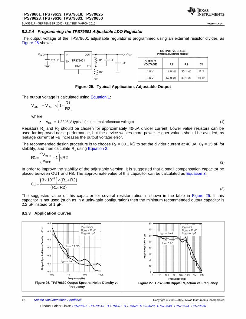
8.2.2.4 Programming the TPS79601 Adjustable LDO RegulatorThe output voltage of the TPS79601 adjustable regulator is programmed using an external resistor divider, asFigure 25 shows.
Figure 25. Typical Application, Adjustable Output
The output voltage is calculated using Equation 1:
where• VREF = 1.2246 V typical (the internal reference voltage) (1)
Resistors R1 and R2 should be chosen for approximately 40-μA divider current. Lower value resistors can beused for improved noise performance, but the device wastes more power. Higher values should be avoided, asleakage current at FB increases the output voltage error.
The recommended design procedure is to choose R2 = 30.1 kΩ to set the divider current at 40 μA, C1 = 15 pF forstability, and then calculate R1 using Equation 2:
(2)
In order to improve the stability of the adjustable version, it is suggested that a small compensation capacitor beplaced between OUT and FB. The approximate value of this capacitor can be calculated as Equation 3:
(3)
The suggested value of this capacitor for several resistor ratios is shown in the table in Figure 25. If thiscapacitor is not used (such as in a unity-gain configuration) then the minimum recommended output capacitor is2.2 μF instead of 1 μF.
8.2.3 Application Curves
Figure 26. TPS79630 Output Spectral Noise Density vs Figure 27. TPS79630 Ripple Rejection vs FrequencyFrequency
16 Submit Documentation Feedback Copyright © 2002–2015, Texas Instruments Incorporated
Product Folder Links: TPS79601 TPS79613 TPS79618 TPS79625 TPS79628 TPS79630 TPS79633 TPS79650

TPS79601, TPS79613, TPS79618, TPS79625TPS79628, TPS79630, TPS79633, TPS79650
www.ti.com SLVS351P –SEPTEMBER 2002–REVISED MARCH 2015
8.3 Do's and Don'tsPlace at least one 1-µF ceramic capacitor as close as possible to the OUT pin of the regulator.
Do not place the output capacitor more than 10 mm away from the regulator.
Connect a 2.2-μF low equivalent series resistance (ESR) capacitor across the IN pin and GND input of theregulator.
Do not exceed the absolute maximum ratings.
9 Power Supply RecommendationsThese devices are designed to operate from an input voltage supply range between 2.7 V and 5.5 V. The inputvoltage range provides adequate headroom in order for the device to have a regulated output. This input supplyis well-regulated and stable. If the input supply is noisy, additional input capacitors with low ESR can helpimprove the output noise performance.
10 Layout
10.1 Layout Guidelines
10.1.1 Board Layout Recommendation to Improve PSRR and Noise PerformanceTo improve AC measurements like PSRR, output noise, and transient response, it is recommended that theboard be designed with separate ground planes for VIN and VOUT, with each ground plane connected only at theground pin of the device. In addition, the ground connection for the bypass capacitor should connect directly tothe ground pin of the device.
10.1.2 Regulator MountingThe tab of the SOT223-6 package is electrically connected to ground. For best thermal performance, the tab ofthe surface-mount version should be soldered directly to a circuit-board copper area. Increasing the copper areaimproves heat dissipation.
Solder pad footprint recommendations for the devices are presented in an application bulletin Solder PadRecommendations for Surface-Mount Devices, SBFA015, available from the TI website (www.ti.com).
Copyright © 2002–2015, Texas Instruments Incorporated Submit Documentation Feedback 17
Product Folder Links: TPS79601 TPS79613 TPS79618 TPS79625 TPS79628 TPS79630 TPS79633 TPS79650

EN
1
2
3
4
8
7
6
5
GND PLANE
CIN
R1
R2
IN N/C
GND
VIN
VOUT
TPS79601DRB
IN
OUT
OUT NR/FB
COUT
GND PLANE
TPS79601, TPS79613, TPS79618, TPS79625TPS79628, TPS79630, TPS79633, TPS79650SLVS351P –SEPTEMBER 2002–REVISED MARCH 2015 www.ti.com
10.2 Layout Examples
Figure 28. TPS79601 (Adjustable Voltage Version)—DRB Layout Example
18 Submit Documentation Feedback Copyright © 2002–2015, Texas Instruments Incorporated
Product Folder Links: TPS79601 TPS79613 TPS79618 TPS79625 TPS79628 TPS79630 TPS79633 TPS79650

AJA
D
125 C TR
PT
q
D IN OUT OUTP V V I u
EN
1
2
3
4
8
7
6
5
GND PLANE
CIN
CNR
IN N/C
GND
VIN
VOUT
TPS796xxDRB
IN
OUT
OUT NR/FB
COUT
GND PLANE
TPS79601, TPS79613, TPS79618, TPS79625TPS79628, TPS79630, TPS79633, TPS79650
www.ti.com SLVS351P –SEPTEMBER 2002–REVISED MARCH 2015
Layout Examples (continued)
Figure 29. TPS796xx (Fixed Voltage Versions)—DRB Layout Example
10.3 Thermal ConsiderationsKnowing the device power dissipation and proper sizing of the thermal plane that is connected to the tab or padis critical to avoiding thermal shutdown and ensuring reliable operation.
Power dissipation of the device depends on input voltage and load conditions and can be calculated usingEquation 4:
(4)
Power dissipation can be minimized and greater efficiency can be achieved by using the lowest possible inputvoltage necessary to achieve the required output voltage regulation.
On the VSON (DRB) package, the primary conduction path for heat is through the exposed pad to the printedcircuit board (PCB). The pad can be connected to ground or be left floating; however, it should be attached to anappropriate amount of copper PCB area to ensure the device does not overheat. On both SOT-223 (DCQ) andTO-263 (KTT) packages, the primary conduction path for heat is through the tab to the PCB. That tab should beconnected to ground. The maximum junction-to-ambient thermal resistance depends on the maximum ambienttemperature, maximum device junction temperature, and power dissipation of the device and can be calculatedusing Equation 5:
' (5)
Knowing the maximum RθJA, the minimum amount of PCB copper area needed for appropriate heatsinking canbe estimated using Figure 30.
Copyright © 2002–2015, Texas Instruments Incorporated Submit Documentation Feedback 19
Product Folder Links: TPS79601 TPS79613 TPS79618 TPS79625 TPS79628 TPS79630 TPS79633 TPS79650

Y YJT J T JT D
: T = T + P·
Y YJB J B JB D
: T = T + P·
160
140
120
100
80
60
40
20
0
qJA
(C
/W)
°
0 1 2 3 4 5 6 7 8 9 10
Board Copper Area ( )in2
DCQ
DRB
KTT
TPS79601, TPS79613, TPS79618, TPS79625TPS79628, TPS79630, TPS79633, TPS79650SLVS351P –SEPTEMBER 2002–REVISED MARCH 2015 www.ti.com
Thermal Considerations (continued)
θJA value at board size of 9in2 (that is, 3in × 3in) is a JEDEC standard.
Figure 30. ΘJA vs Board Size
Figure 30 shows the variation of θJA as a function of ground plane copper area in the board. It is intended only asa guideline to demonstrate the effects of heat spreading in the ground plane and should not be used to estimateactual thermal performance in real application environments.
NOTEWhen the device is mounted on an application PCB, it is strongly recommended to useΨJT and ΨJB, as explained in Estimating Junction Temperature.
10.4 Estimating Junction TemperatureUsing the thermal metrics ΨJT and ΨJB, as shown in Thermal Information, the junction temperature can beestimated with corresponding formulas (given in Equation 6). For backwards compatibility, an older θJC,Topparameter is listed as well.
where• PD is the power dissipation shown by Equation 5• TT is the temperature at the center-top of the IC package• TB is the PCB temperature measured 1mm away from the IC package on the PCB surface (as Figure 32
shows). (6)
NOTEBoth TT and TB can be measured on actual application boards using a thermo-gun (aninfrared thermometer).
For more information about measuring TT and TB, see the application note SBVA025, Using New ThermalMetrics, available at www.ti.com.
By looking at Figure 31, the new thermal metrics (ΨJT and ΨJB) have very little dependency on board size. Thatis, using ΨJT or ΨJB with Equation 6 is a good way to estimate TJ by simply measuring TT or TB, regardless of theapplication board size.
20 Submit Documentation Feedback Copyright © 2002–2015, Texas Instruments Incorporated
Product Folder Links: TPS79601 TPS79613 TPS79618 TPS79625 TPS79628 TPS79630 TPS79633 TPS79650

(a) Example DRB (VSON) Package Measurement (b) Example DCQ (SOT-223) Package Measurement
1mm
T on topT
of IC
T on PCBB
surface
(c) Example KTT (TO-263) Package Measurement
1mm X
X
TT
TB
1mm
T on of ICT top(1)
T on PCBB
surface(2)
35
30
25
20
15
10
5
0
YY
and
(C
/W)
JT
JB
°
0 2 4 6 8 10
Board Copper Area (in )2
51 3 7 9
DCQ YJT
DCQ
DRB
KTT
KTT YJTDRB YJT
YJB
TPS79601, TPS79613, TPS79618, TPS79625TPS79628, TPS79630, TPS79633, TPS79650
www.ti.com SLVS351P –SEPTEMBER 2002–REVISED MARCH 2015
Estimating Junction Temperature (continued)
Figure 31. ΨJT And ΨJB vs Board Size
For a more detailed discussion of why TI does not recommend using θJC(top) to determine thermal characteristics,refer to application report SBVA025, Using New Thermal Metrics, available for download at www.ti.com. Forfurther information, refer to application report SPRA953, IC Package Thermal Metrics, also available on the TIwebsite.
(1) TT is measured at the center of both the X- and Y-dimensional axes.(2) TB is measured below the package lead on the PCB surface.
Figure 32. Measuring Points For TT and TB
Copyright © 2002–2015, Texas Instruments Incorporated Submit Documentation Feedback 21
Product Folder Links: TPS79601 TPS79613 TPS79618 TPS79625 TPS79628 TPS79630 TPS79633 TPS79650

TPS79601, TPS79613, TPS79618, TPS79625TPS79628, TPS79630, TPS79633, TPS79650SLVS351P –SEPTEMBER 2002–REVISED MARCH 2015 www.ti.com
11 Device and Documentation Support
11.1 Device Support
11.1.1 Development Support
11.1.1.1 Evaluation ModulesAn evaluation module (EVM) is available to assist in the initial circuit performance evaluation using the TPS796.The TPS79601DRBEVM evaluation module can be requested at the TI website through the product folders orpurchased directly from the TI eStore.
11.1.1.2 Spice ModelsComputer simulation of circuit performance using SPICE is often useful when analyzing the performance ofanalog circuits and systems. A SPICE model for the TPS796 is available through the product folders undersimulation models.
11.1.2 Device Nomenclature
Table 3. Device Nomenclature (1)
PRODUCT VOUT
TPS796xx(x) yyy z xx(x) is nominal output voltage (for example, 28 = 2.8 V, 285 = 2.85 V, 01 = Adjustable).yyy is package designator.z is package quantity.
(1) For the most current package and ordering information see the Package Option Addendum at the end of this document, or visit thedevice product folder at www.ti.com.
11.2 Documentation Support
11.2.1 Related DocumentationFor related documentation, see the following:• Using New Thermal Metrics, SBVA025• IC Package Thermal Metrics, SPRA953• TPS79601DRBEVM User's Guide, SLVU130• Solder Pad Recommendations for Surface-Mount Devices, SBFA015
11.3 Related LinksThe table below lists quick access links. Categories include technical documents, support and communityresources, tools and software, and quick access to sample or buy.
Table 4. Related LinksTECHNICAL TOOLS & SUPPORT &PARTS PRODUCT FOLDER SAMPLE & BUY DOCUMENTS SOFTWARE COMMUNITY
TPS79601 Click here Click here Click here Click here Click hereTPS79613 Click here Click here Click here Click here Click hereTPS79618 Click here Click here Click here Click here Click hereTPS79625 Click here Click here Click here Click here Click hereTPS79628 Click here Click here Click here Click here Click hereTPS79630 Click here Click here Click here Click here Click hereTPS79633 Click here Click here Click here Click here Click hereTPS79650 Click here Click here Click here Click here Click hereTPS79601 Click here Click here Click here Click here Click hereTPS79613 Click here Click here Click here Click here Click hereTPS79618 Click here Click here Click here Click here Click here
22 Submit Documentation Feedback Copyright © 2002–2015, Texas Instruments Incorporated
Product Folder Links: TPS79601 TPS79613 TPS79618 TPS79625 TPS79628 TPS79630 TPS79633 TPS79650

TPS79601, TPS79613, TPS79618, TPS79625TPS79628, TPS79630, TPS79633, TPS79650
www.ti.com SLVS351P –SEPTEMBER 2002–REVISED MARCH 2015
Related Links (continued)Table 4. Related Links (continued)
TECHNICAL TOOLS & SUPPORT &PARTS PRODUCT FOLDER SAMPLE & BUY DOCUMENTS SOFTWARE COMMUNITYTPS79625 Click here Click here Click here Click here Click hereTPS79628 Click here Click here Click here Click here Click hereTPS79630 Click here Click here Click here Click here Click hereTPS79633 Click here Click here Click here Click here Click hereTPS79650 Click here Click here Click here Click here Click here
11.4 TrademarksPowerPAD is a trademark of Texas Instruments Inc.Bluetooth is a registered trademark of Bluetooth SIG, Inc.All other trademarks are the property of their respective owners.
11.5 Electrostatic Discharge CautionThis integrated circuit can be damaged by ESD. Texas Instruments recommends that all integrated circuits be handled withappropriate precautions. Failure to observe proper handling and installation procedures can cause damage.
ESD damage can range from subtle performance degradation to complete device failure. Precision integrated circuits may be moresusceptible to damage because very small parametric changes could cause the device not to meet its published specifications.
11.6 GlossarySLYZ022 — TI Glossary.
This glossary lists and explains terms, acronyms, and definitions.
12 Mechanical, Packaging, and Orderable InformationThe following pages include mechanical, packaging, and orderable information. This information is the mostcurrent data available for the designated devices. This data is subject to change without notice and revision ofthis document. For browser-based versions of this data sheet, refer to the left-hand navigation.
Copyright © 2002–2015, Texas Instruments Incorporated Submit Documentation Feedback 23
Product Folder Links: TPS79601 TPS79613 TPS79618 TPS79625 TPS79628 TPS79630 TPS79633 TPS79650

PACKAGE OPTION ADDENDUM
www.ti.com 18-Aug-2022
PACKAGING INFORMATION
Orderable Device Status(1)
Package Type PackageDrawing
Pins PackageQty
Eco Plan(2)
Lead finish/Ball material
(6)
MSL Peak Temp(3)
Op Temp (°C) Device Marking(4/5)
Samples
TPS79601DCQ ACTIVE SOT-223 DCQ 6 78 RoHS & Green SN Level-2-260C-1 YEAR -40 to 125 PS79601 Samples
TPS79601DCQG4 ACTIVE SOT-223 DCQ 6 78 RoHS & Green NIPDAU Level-2-260C-1 YEAR -40 to 125 PS79601 Samples
TPS79601DCQR ACTIVE SOT-223 DCQ 6 2500 RoHS & Green SN Level-2-260C-1 YEAR -40 to 125 PS79601 Samples
TPS79601DRBR ACTIVE SON DRB 8 3000 RoHS & Green NIPDAU Level-2-260C-1 YEAR -40 to 125 CES Samples
TPS79601DRBRG4 ACTIVE SON DRB 8 3000 RoHS & Green NIPDAU Level-2-260C-1 YEAR -40 to 125 CES Samples
TPS79601DRBT ACTIVE SON DRB 8 250 RoHS & Green NIPDAU Level-2-260C-1 YEAR -40 to 125 CES Samples
TPS79601DRBTG4 ACTIVE SON DRB 8 250 RoHS & Green NIPDAU Level-2-260C-1 YEAR -40 to 125 CES Samples
TPS79601KTTR ACTIVE DDPAK/TO-263
KTT 5 500 RoHS & Green SN Level-2-260C-1 YEAR -40 to 125 TPS79601
Samples
TPS79601KTTRG3 ACTIVE DDPAK/TO-263
KTT 5 500 RoHS & Green SN Level-2-260C-1 YEAR -40 to 125 TPS79601
Samples
TPS79613DRBR ACTIVE SON DRB 8 3000 RoHS & Green NIPDAU Level-2-260C-1 YEAR -40 to 85 CCT Samples
TPS79618DCQ ACTIVE SOT-223 DCQ 6 78 RoHS & Green NIPDAU Level-2-260C-1 YEAR -40 to 125 PS79618 Samples
TPS79618DCQR ACTIVE SOT-223 DCQ 6 2500 RoHS & Green SN Level-2-260C-1 YEAR -40 to 125 PS79618 Samples
TPS79618DCQRG4 ACTIVE SOT-223 DCQ 6 2500 RoHS & Green NIPDAU Level-2-260C-1 YEAR -40 to 125 PS79618 Samples
TPS79618KTTR ACTIVE DDPAK/TO-263
KTT 5 500 RoHS & Green SN Level-2-260C-1 YEAR TPS79618
Samples
TPS79625DCQ ACTIVE SOT-223 DCQ 6 78 RoHS & Green NIPDAU Level-2-260C-1 YEAR -40 to 125 PS79625 Samples
TPS79625DCQR ACTIVE SOT-223 DCQ 6 2500 RoHS & Green SN Level-2-260C-1 YEAR -40 to 125 PS79625 Samples
TPS79625DCQRG4 ACTIVE SOT-223 DCQ 6 2500 RoHS & Green NIPDAU Level-2-260C-1 YEAR -40 to 125 PS79625 Samples
TPS79625KTTR ACTIVE DDPAK/TO-263
KTT 5 500 RoHS & Green SN Level-2-260C-1 YEAR TPS79625
Samples
TPS79628DCQ ACTIVE SOT-223 DCQ 6 78 RoHS & Green NIPDAU Level-2-260C-1 YEAR -40 to 125 PS79628 Samples
Addendum-Page 1

PACKAGE OPTION ADDENDUM
www.ti.com 18-Aug-2022
Orderable Device Status(1)
Package Type PackageDrawing
Pins PackageQty
Eco Plan(2)
Lead finish/Ball material
(6)
MSL Peak Temp(3)
Op Temp (°C) Device Marking(4/5)
Samples
TPS79628DCQR ACTIVE SOT-223 DCQ 6 2500 RoHS & Green NIPDAU Level-2-260C-1 YEAR -40 to 125 PS79628 Samples
TPS79628DRBT ACTIVE SON DRB 8 250 RoHS & Green NIPDAU Level-2-260C-1 YEAR -40 to 85 AMI Samples
TPS79630DCQ ACTIVE SOT-223 DCQ 6 78 RoHS & Green NIPDAU Level-2-260C-1 YEAR -40 to 125 PS79630 Samples
TPS79630DCQG4 ACTIVE SOT-223 DCQ 6 78 RoHS & Green NIPDAU Level-2-260C-1 YEAR -40 to 125 PS79630 Samples
TPS79630DCQR ACTIVE SOT-223 DCQ 6 2500 RoHS & Green NIPDAU Level-2-260C-1 YEAR -40 to 125 PS79630 Samples
TPS79630KTTR ACTIVE DDPAK/TO-263
KTT 5 500 RoHS & Green SN Level-2-260C-1 YEAR TPS79630
Samples
TPS79633DCQ ACTIVE SOT-223 DCQ 6 78 RoHS & Green SN Level-2-260C-1 YEAR -40 to 125 PS79633 Samples
TPS79633DCQG4 ACTIVE SOT-223 DCQ 6 78 RoHS & Green NIPDAU Level-2-260C-1 YEAR -40 to 125 PS79633 Samples
TPS79633DCQR ACTIVE SOT-223 DCQ 6 2500 RoHS & Green SN Level-2-260C-1 YEAR -40 to 125 PS79633 Samples
TPS79633DCQRG4 ACTIVE SOT-223 DCQ 6 2500 RoHS & Green NIPDAU Level-2-260C-1 YEAR -40 to 125 PS79633 Samples
TPS79633KTTR ACTIVE DDPAK/TO-263
KTT 5 500 RoHS & Green SN Level-2-260C-1 YEAR TPS79633
Samples
TPS79633KTTRG3 ACTIVE DDPAK/TO-263
KTT 5 500 RoHS & Green SN Level-2-260C-1 YEAR -40 to 125 TPS79633
Samples
TPS79650DCQ ACTIVE SOT-223 DCQ 6 78 RoHS & Green NIPDAU Level-2-260C-1 YEAR -40 to 125 PS79650 Samples
TPS79650DCQG4 ACTIVE SOT-223 DCQ 6 78 RoHS & Green NIPDAU Level-2-260C-1 YEAR -40 to 125 PS79650 Samples
TPS79650DCQR ACTIVE SOT-223 DCQ 6 2500 RoHS & Green NIPDAU Level-2-260C-1 YEAR -40 to 125 PS79650 Samples
TPS79650DRBR ACTIVE SON DRB 8 3000 RoHS & Green NIPDAU Level-2-260C-1 YEAR -40 to 125 BYZ Samples
TPS79650DRBT ACTIVE SON DRB 8 250 RoHS & Green NIPDAU Level-2-260C-1 YEAR -40 to 125 BYZ Samples
TPS79650DRBTG4 ACTIVE SON DRB 8 250 RoHS & Green NIPDAU Level-2-260C-1 YEAR -40 to 125 BYZ Samples
(1) The marketing status values are defined as follows:ACTIVE: Product device recommended for new designs.LIFEBUY: TI has announced that the device will be discontinued, and a lifetime-buy period is in effect.NRND: Not recommended for new designs. Device is in production to support existing customers, but TI does not recommend using this part in a new design.
Addendum-Page 2

PACKAGE OPTION ADDENDUM
www.ti.com 18-Aug-2022
PREVIEW: Device has been announced but is not in production. Samples may or may not be available.OBSOLETE: TI has discontinued the production of the device.
(2) RoHS: TI defines "RoHS" to mean semiconductor products that are compliant with the current EU RoHS requirements for all 10 RoHS substances, including the requirement that RoHS substancedo not exceed 0.1% by weight in homogeneous materials. Where designed to be soldered at high temperatures, "RoHS" products are suitable for use in specified lead-free processes. TI mayreference these types of products as "Pb-Free".RoHS Exempt: TI defines "RoHS Exempt" to mean products that contain lead but are compliant with EU RoHS pursuant to a specific EU RoHS exemption.Green: TI defines "Green" to mean the content of Chlorine (Cl) and Bromine (Br) based flame retardants meet JS709B low halogen requirements of <=1000ppm threshold. Antimony trioxide basedflame retardants must also meet the <=1000ppm threshold requirement.
(3) MSL, Peak Temp. - The Moisture Sensitivity Level rating according to the JEDEC industry standard classifications, and peak solder temperature.
(4) There may be additional marking, which relates to the logo, the lot trace code information, or the environmental category on the device.
(5) Multiple Device Markings will be inside parentheses. Only one Device Marking contained in parentheses and separated by a "~" will appear on a device. If a line is indented then it is a continuationof the previous line and the two combined represent the entire Device Marking for that device.
(6) Lead finish/Ball material - Orderable Devices may have multiple material finish options. Finish options are separated by a vertical ruled line. Lead finish/Ball material values may wrap to twolines if the finish value exceeds the maximum column width.
Important Information and Disclaimer:The information provided on this page represents TI's knowledge and belief as of the date that it is provided. TI bases its knowledge and belief on informationprovided by third parties, and makes no representation or warranty as to the accuracy of such information. Efforts are underway to better integrate information from third parties. TI has taken andcontinues to take reasonable steps to provide representative and accurate information but may not have conducted destructive testing or chemical analysis on incoming materials and chemicals.TI and TI suppliers consider certain information to be proprietary, and thus CAS numbers and other limited information may not be available for release.
In no event shall TI's liability arising out of such information exceed the total purchase price of the TI part(s) at issue in this document sold by TI to Customer on an annual basis.
Addendum-Page 3

PACKAGE MATERIALS INFORMATION
www.ti.com 3-Jun-2022
TAPE AND REEL INFORMATION
Reel Width (W1)
REEL DIMENSIONS
A0B0K0W
Dimension designed to accommodate the component lengthDimension designed to accommodate the component thicknessOverall width of the carrier tapePitch between successive cavity centers
Dimension designed to accommodate the component width
TAPE DIMENSIONS
K0 P1
B0 W
A0Cavity
QUADRANT ASSIGNMENTS FOR PIN 1 ORIENTATION IN TAPE
Pocket Quadrants
Sprocket Holes
Q1 Q1Q2 Q2
Q3 Q3Q4 Q4 User Direction of Feed
P1
ReelDiameter
*All dimensions are nominal
Device PackageType
PackageDrawing
Pins SPQ ReelDiameter
(mm)
ReelWidth
W1 (mm)
A0(mm)
B0(mm)
K0(mm)
P1(mm)
W(mm)
Pin1Quadrant
TPS79601DCQR SOT-223 DCQ 6 2500 330.0 12.4 7.1 7.45 1.88 8.0 12.0 Q3
TPS79601DRBR SON DRB 8 3000 330.0 12.4 3.3 3.3 1.1 8.0 12.0 Q2
TPS79601DRBT SON DRB 8 250 180.0 12.4 3.3 3.3 1.1 8.0 12.0 Q2
TPS79601KTTR DDPAK/TO-263
KTT 5 500 330.0 24.4 10.6 15.6 4.9 16.0 24.0 Q2
TPS79613DRBR SON DRB 8 3000 330.0 12.4 3.3 3.3 1.1 8.0 12.0 Q2
TPS79618DCQR SOT-223 DCQ 6 2500 330.0 12.4 7.1 7.45 1.88 8.0 12.0 Q3
TPS79618DCQRG4 SOT-223 DCQ 6 2500 330.0 12.4 7.1 7.45 1.88 8.0 12.0 Q3
TPS79618KTTR DDPAK/TO-263
KTT 5 500 330.0 24.4 10.6 15.6 4.9 16.0 24.0 Q2
TPS79625DCQR SOT-223 DCQ 6 2500 330.0 12.4 7.1 7.45 1.88 8.0 12.0 Q3
TPS79625DCQRG4 SOT-223 DCQ 6 2500 330.0 12.4 7.1 7.45 1.88 8.0 12.0 Q3
TPS79625KTTR DDPAK/TO-263
KTT 5 500 330.0 24.4 10.6 15.6 4.9 16.0 24.0 Q2
TPS79628DCQR SOT-223 DCQ 6 2500 330.0 12.4 7.1 7.45 1.88 8.0 12.0 Q3
TPS79628DRBT SON DRB 8 250 180.0 12.4 3.3 3.3 1.1 8.0 12.0 Q2
TPS79630DCQR SOT-223 DCQ 6 2500 330.0 12.4 7.1 7.45 1.88 8.0 12.0 Q3
Pack Materials-Page 1

PACKAGE MATERIALS INFORMATION
www.ti.com 3-Jun-2022
Device PackageType
PackageDrawing
Pins SPQ ReelDiameter
(mm)
ReelWidth
W1 (mm)
A0(mm)
B0(mm)
K0(mm)
P1(mm)
W(mm)
Pin1Quadrant
TPS79630KTTR DDPAK/TO-263
KTT 5 500 330.0 24.4 10.6 15.6 4.9 16.0 24.0 Q2
TPS79633DCQR SOT-223 DCQ 6 2500 330.0 12.4 7.1 7.45 1.88 8.0 12.0 Q3
TPS79633DCQRG4 SOT-223 DCQ 6 2500 330.0 12.4 7.1 7.45 1.88 8.0 12.0 Q3
TPS79633KTTR DDPAK/TO-263
KTT 5 500 330.0 24.4 10.6 15.6 4.9 16.0 24.0 Q2
TPS79650DCQR SOT-223 DCQ 6 2500 330.0 12.4 7.1 7.45 1.88 8.0 12.0 Q3
TPS79650DRBR SON DRB 8 3000 330.0 12.4 3.3 3.3 1.1 8.0 12.0 Q2
TPS79650DRBT SON DRB 8 250 180.0 12.4 3.3 3.3 1.1 8.0 12.0 Q2
Pack Materials-Page 2

PACKAGE MATERIALS INFORMATION
www.ti.com 3-Jun-2022
TAPE AND REEL BOX DIMENSIONS
Width (mm)
W L
H
*All dimensions are nominal
Device Package Type Package Drawing Pins SPQ Length (mm) Width (mm) Height (mm)
TPS79601DCQR SOT-223 DCQ 6 2500 356.0 356.0 35.0
TPS79601DRBR SON DRB 8 3000 356.0 356.0 35.0
TPS79601DRBT SON DRB 8 250 210.0 185.0 35.0
TPS79601KTTR DDPAK/TO-263 KTT 5 500 367.0 367.0 45.0
TPS79613DRBR SON DRB 8 3000 356.0 356.0 35.0
TPS79618DCQR SOT-223 DCQ 6 2500 356.0 356.0 35.0
TPS79618DCQRG4 SOT-223 DCQ 6 2500 346.0 346.0 41.0
TPS79618KTTR DDPAK/TO-263 KTT 5 500 367.0 367.0 45.0
TPS79625DCQR SOT-223 DCQ 6 2500 356.0 356.0 35.0
TPS79625DCQRG4 SOT-223 DCQ 6 2500 358.0 335.0 35.0
TPS79625KTTR DDPAK/TO-263 KTT 5 500 367.0 367.0 45.0
TPS79628DCQR SOT-223 DCQ 6 2500 346.0 346.0 29.0
TPS79628DRBT SON DRB 8 250 210.0 185.0 35.0
TPS79630DCQR SOT-223 DCQ 6 2500 346.0 346.0 29.0
TPS79630KTTR DDPAK/TO-263 KTT 5 500 367.0 367.0 45.0
TPS79633DCQR SOT-223 DCQ 6 2500 356.0 356.0 35.0
TPS79633DCQRG4 SOT-223 DCQ 6 2500 346.0 346.0 41.0
TPS79633KTTR DDPAK/TO-263 KTT 5 500 367.0 367.0 45.0
Pack Materials-Page 3

PACKAGE MATERIALS INFORMATION
www.ti.com 3-Jun-2022
Device Package Type Package Drawing Pins SPQ Length (mm) Width (mm) Height (mm)
TPS79650DCQR SOT-223 DCQ 6 2500 346.0 346.0 29.0
TPS79650DRBR SON DRB 8 3000 356.0 356.0 35.0
TPS79650DRBT SON DRB 8 250 210.0 185.0 35.0
Pack Materials-Page 4

PACKAGE MATERIALS INFORMATION
www.ti.com 3-Jun-2022
TUBE
L - Tube lengthT - Tube height
W - Tube width
B - Alignment groove width *All dimensions are nominal
Device Package Name Package Type Pins SPQ L (mm) W (mm) T (µm) B (mm)
TPS79601DCQ DCQ SOT-223 6 78 543 8.6 3606.8 2.67
TPS79601DCQG4 DCQ SOT-223 6 78 532.13 8.63 3.6 3.68
TPS79618DCQ DCQ SOT-223 6 78 532.13 8.63 3.6 3.68
TPS79625DCQ DCQ SOT-223 6 78 532.13 8.63 3.6 3.68
TPS79628DCQ DCQ SOT-223 6 78 532.13 8.63 3.6 3.68
TPS79630DCQ DCQ SOT-223 6 78 532.13 8.63 3.6 3.68
TPS79630DCQG4 DCQ SOT-223 6 78 532.13 8.63 3.6 3.68
TPS79633DCQ DCQ SOT-223 6 78 543 8.6 3606.8 2.67
TPS79633DCQG4 DCQ SOT-223 6 78 532.13 8.63 3.6 3.68
TPS79650DCQ DCQ SOT-223 6 78 532.13 8.63 3.6 3.68
TPS79650DCQG4 DCQ SOT-223 6 78 532.13 8.63 3.6 3.68
Pack Materials-Page 5


www.ti.com
PACKAGE OUTLINE
C
7.266.86
5.08
5X 0.510.41
1.27TYP
3.052.95
1.8 MAX
0.100.02
0.320.240.25
GAGE PLANE
A
6.66.4
NOTE 3
B3.63.4
NOTE 3
1.140.910 -8
TYP
(1.6)
SOT - 1.8 mm max heightDCQ0006APLASTIC SMALL OUTLINE
4214845/C 11/2021
NOTES: 1. All linear dimensions are in millimeters. Any dimensions in parenthesis are for reference only. Dimensioning and tolerancing per ASME Y14.5M.2. This drawing is subject to change without notice.3. This dimension does not include mold flash, protrusions, or gate burrs. Mold flash, protrusions, or gate burrs shall not exceed 0.15 mm per side.
0.1 C A B
0.1 C A B
1
5
6
PIN 1INDEX AREA
SEATING PLANE
0.08
SCALE 2.000

www.ti.com
EXAMPLE BOARD LAYOUT
5X (2.05)
5X (0.65)
0.2 TYP
0.07 MAXALL AROUND
0.07 MINALL AROUND
(6)
(2.05)
(3.2)
4X (1.27)
(R0.05) TYP
(1.35)
(0.775) TYP
SOT - 1.8 mm max heightDCQ0006APLASTIC SMALL OUTLINE
4214845/C 11/2021
NOTES: (continued) 4. Publication IPC-7351 may have alternate designs. 5. Solder mask tolerances between and around signal pads can vary based on board fabrication site.6. Vias are optional depending on application, refer to device data sheet. If any vias are implemented, refer to their locations shown on this view. It is recommended that vias under paste be filled, plugged or tented.
SOLDER MASK DETAILS
LAND PATTERN EXAMPLEEXPOSED METAL SHOWN
SCALE: 10X
SYMM
PKG
1
5
6
METALSOLDER MASKOPENING
EXPOSED METAL
SOLDER MASKOPENING
METAL UNDERSOLDER MASK
EXPOSED METAL

www.ti.com
EXAMPLE STENCIL DESIGN
(6)
(1.27) TYP
(R0.05) TYP
5X (2.05)
5X (0.65)
(0.755)
4X (1.31)
4X (0.92)
(0.56) TYP
SOT - 1.8 mm max heightDCQ0006APLASTIC SMALL OUTLINE
4214845/C 11/2021
NOTES: (continued) 7. Laser cutting apertures with trapezoidal walls and rounded corners may offer better paste release. IPC-7525 may have alternate design recommendations. 8. Board assembly site may have different recommendations for stencil design.
SOLDER PASTE EXAMPLEBASED ON 0.125 mm THICK STENCIL
SCALE: 10X
SYMM
SYMM
1
5
6


www.ti.com
PACKAGE OUTLINE
C
8X 0.350.25
2.4 0.052X
1.95
1.65 0.05
6X 0.65
1 MAX
8X 0.50.3
0.050.00
A 3.12.9
B
3.12.9
(0.2) TYP
VSON - 1 mm max heightDRB0008BPLASTIC SMALL OUTLINE - NO LEAD
4218876/A 12/2017
PIN 1 INDEX AREA
SEATING PLANE
0.08 C
1
4 5
8
(OPTIONAL)PIN 1 ID 0.1 C A B
0.05 C
THERMAL PADEXPOSED
NOTES: 1. All linear dimensions are in millimeters. Any dimensions in parenthesis are for reference only. Dimensioning and tolerancing per ASME Y14.5M. 2. This drawing is subject to change without notice. 3. The package thermal pad must be soldered to the printed circuit board for thermal and mechanical performance.
SCALE 4.000

www.ti.com
EXAMPLE BOARD LAYOUT
0.07 MINALL AROUND
0.07 MAXALL AROUND
8X (0.3)
(2.4)
(2.8)
6X (0.65)
(1.65)
( 0.2) VIATYP
(0.575)
(0.95)
8X (0.6)
(R0.05) TYP
VSON - 1 mm max heightDRB0008BPLASTIC SMALL OUTLINE - NO LEAD
4218876/A 12/2017
SYMM
1
45
8
LAND PATTERN EXAMPLESCALE:20X
NOTES: (continued) 4. This package is designed to be soldered to a thermal pad on the board. For more information, see Texas Instruments literature number SLUA271 (www.ti.com/lit/slua271).5. Vias are optional depending on application, refer to device data sheet. If any vias are implemented, refer to their locations shown on this view. It is recommended that vias under paste be filled, plugged or tented.
SOLDER MASKOPENINGSOLDER MASK
METAL UNDER
SOLDER MASKDEFINED
METALSOLDER MASKOPENING
SOLDER MASK DETAILS
NON SOLDER MASKDEFINED
(PREFERRED)

www.ti.com
EXAMPLE STENCIL DESIGN
(R0.05) TYP
8X (0.3)
8X (0.6)
(1.47)
(1.06)
(2.8)
(0.63)
6X (0.65)
VSON - 1 mm max heightDRB0008BPLASTIC SMALL OUTLINE - NO LEAD
4218876/A 12/2017
NOTES: (continued) 6. Laser cutting apertures with trapezoidal walls and rounded corners may offer better paste release. IPC-7525 may have alternate design recommendations.
SOLDER PASTE EXAMPLEBASED ON 0.125 mm THICK STENCIL
EXPOSED PAD
81% PRINTED SOLDER COVERAGE BY AREASCALE:25X
SYMM
1
4 5
8
METALTYP
SYMM

IMPORTANT NOTICE AND DISCLAIMERTI PROVIDES TECHNICAL AND RELIABILITY DATA (INCLUDING DATA SHEETS), DESIGN RESOURCES (INCLUDING REFERENCE DESIGNS), APPLICATION OR OTHER DESIGN ADVICE, WEB TOOLS, SAFETY INFORMATION, AND OTHER RESOURCES “AS IS” AND WITH ALL FAULTS, AND DISCLAIMS ALL WARRANTIES, EXPRESS AND IMPLIED, INCLUDING WITHOUT LIMITATION ANY IMPLIED WARRANTIES OF MERCHANTABILITY, FITNESS FOR A PARTICULAR PURPOSE OR NON-INFRINGEMENT OF THIRD PARTY INTELLECTUAL PROPERTY RIGHTS.These resources are intended for skilled developers designing with TI products. You are solely responsible for (1) selecting the appropriate TI products for your application, (2) designing, validating and testing your application, and (3) ensuring your application meets applicable standards, and any other safety, security, regulatory or other requirements.These resources are subject to change without notice. TI grants you permission to use these resources only for development of an application that uses the TI products described in the resource. Other reproduction and display of these resources is prohibited. No license is granted to any other TI intellectual property right or to any third party intellectual property right. TI disclaims responsibility for, and you will fully indemnify TI and its representatives against, any claims, damages, costs, losses, and liabilities arising out of your use of these resources.TI’s products are provided subject to TI’s Terms of Sale or other applicable terms available either on ti.com or provided in conjunction with such TI products. TI’s provision of these resources does not expand or otherwise alter TI’s applicable warranties or warranty disclaimers for TI products.TI objects to and rejects any additional or different terms you may have proposed. IMPORTANT NOTICE
Mailing Address: Texas Instruments, Post Office Box 655303, Dallas, Texas 75265Copyright © 2022, Texas Instruments Incorporated
Copyright © 2022 FDOKUMEN