TPA6102A2: 50-mW Ultralow-Voltage, Fixed-Gain Stereo ...
25
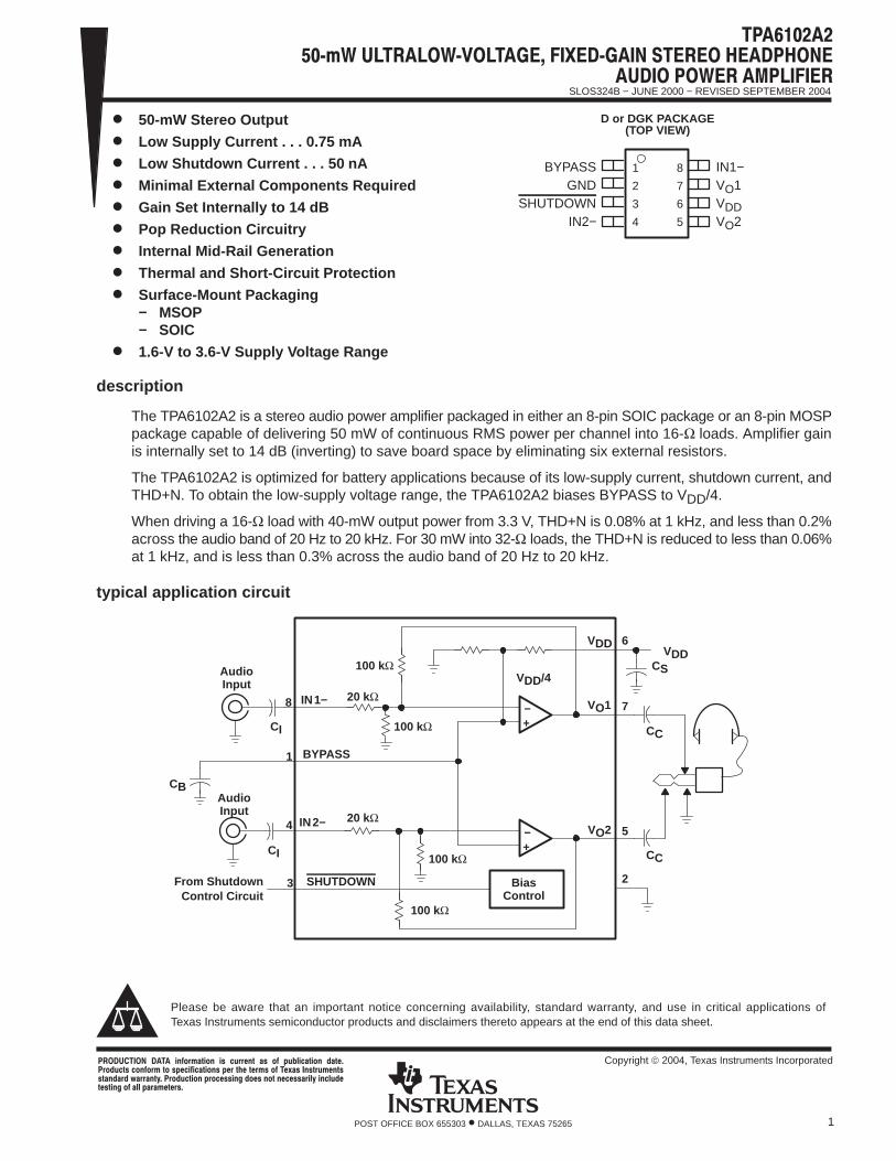
Please be aware that an important notice concerning availability, standard warranty, and use in critical applications of Texas Instruments semiconductor products and disclaimers thereto appears at the end of this data sheet. TPA6102A2 50ĆmW ULTRALOWĆVOLTAGE, FIXEDĆGAIN STEREO HEADPHONE AUDIO POWER AMPLIFIER SLOS324B - JUNE 2000 - REVISED SEPTEMBER 2004 1 POST OFFICE BOX 655303 • DALLAS, TEXAS 75265 D 50-mW Stereo Output D Low Supply Current . . . 0.75 mA D Low Shutdown Current . . . 50 nA D Minimal External Components Required D Gain Set Internally to 14 dB D Pop Reduction Circuitry D Internal Mid-Rail Generation D Thermal and Short-Circuit Protection D Surface-Mount Packaging - MSOP - SOIC D 1.6-V to 3.6-V Supply Voltage Range description The TPA6102A2 is a stereo audio power amplifier packaged in either an 8-pin SOIC package or an 8-pin MOSP package capable of delivering 50 mW of continuous RMS power per channel into 16-Ω loads. Amplifier gain is internally set to 14 dB (inverting) to save board space by eliminating six external resistors. The TPA6102A2 is optimized for battery applications because of its low-supply current, shutdown current, and THD+N. To obtain the low-supply voltage range, the TPA6102A2 biases BYPASS to V DD /4. When driving a 16-Ω load with 40-mW output power from 3.3 V, THD+N is 0.08% at 1 kHz, and less than 0.2% across the audio band of 20 Hz to 20 kHz. For 30 mW into 32-Ω loads, the THD+N is reduced to less than 0.06% at 1 kHz, and is less than 0.3% across the audio band of 20 Hz to 20 kHz. typical application circuit Audio Input Bias Control 6 7 5 2 V O 1 V O 2 V DD 3 8 1 4 IN 1- BYPASS SHUTDOWN V DD /4 C I 20 kΩ 100 kΩ C B C S Audio Input C I IN 2- V DD From Shutdown Control Circuit - + - + C C C C 100 kΩ 20 kΩ 100 kΩ 100 kΩ 1 2 3 4 8 7 6 5 BYPASS GND SHUTDOWN IN2- IN1- V O 1 V DD V O 2 D or DGK PACKAGE (TOP VIEW) Copyright 2004, Texas Instruments Incorporated PRODUCTION DATA information is current as of publication date. Products conform to specifications per the terms of Texas Instruments standard warranty. Production processing does not necessarily include testing of all parameters.
-
Upload
khangminh22 -
Category
Documents
-
view
3 -
download
0
Transcript of TPA6102A2: 50-mW Ultralow-Voltage, Fixed-Gain Stereo ...
Please be aware that an important notice concerning availability, standard warranty, and use in critical applications ofTexas Instruments semiconductor products and disclaimers thereto appears at the end of this data sheet.
SLOS324B − JUNE 2000 − REVISED SEPTEMBER 2004
1POST OFFICE BOX 655303 • DALLAS, TEXAS 75265
50-mW Stereo Output
Low Supply Current . . . 0.75 mA
Low Shutdown Current . . . 50 nA
Minimal External Components Required
Gain Set Internally to 14 dB
Pop Reduction Circuitry
Internal Mid-Rail Generation
Thermal and Short-Circuit Protection
Surface-Mount Packaging− MSOP− SOIC
1.6-V to 3.6-V Supply Voltage Range
description
The TPA6102A2 is a stereo audio power amplifier packaged in either an 8-pin SOIC package or an 8-pin MOSPpackage capable of delivering 50 mW of continuous RMS power per channel into 16-Ω loads. Amplifier gainis internally set to 14 dB (inverting) to save board space by eliminating six external resistors.
The TPA6102A2 is optimized for battery applications because of its low-supply current, shutdown current, andTHD+N. To obtain the low-supply voltage range, the TPA6102A2 biases BYPASS to VDD/4.
When driving a 16-Ω load with 40-mW output power from 3.3 V, THD+N is 0.08% at 1 kHz, and less than 0.2%across the audio band of 20 Hz to 20 kHz. For 30 mW into 32-Ω loads, the THD+N is reduced to less than 0.06%at 1 kHz, and is less than 0.3% across the audio band of 20 Hz to 20 kHz.
typical application circuit
AudioInput
BiasControl
6
7
5
2
VO1
VO2
VDD
3
8
1
4
IN1−
BYPASS
SHUTDOWN
VDD/4
CI
20 kΩ
100 kΩ
CB
CS
AudioInput
CI
IN2−
VDD
From ShutdownControl Circuit
−+
−+
CC
CC
100 kΩ
20 kΩ
100 kΩ
100 kΩ
1
2
3
4
8
7
6
5
BYPASSGND
SHUTDOWNIN2−
IN1−VO1VDDVO2
D or DGK PACKAGE(TOP VIEW)
Copyright 2004, Texas Instruments Incorporated !"#$! % &'""($ #% ! )'*+&#$! ,#$(-"!,'&$% &!!" $! %)(&&#$!% )(" $.( $("% ! (/#% %$"'($%%$#,#", 0#""#$1- "!,'&$! )"!&(%%2 ,!(% !$ (&(%%#"+1 &+',($(%$2 ! #++ )#"#($("%-
SLOS324B − JUNE 2000 − REVISED SEPTEMBER 2004
2 POST OFFICE BOX 655303 • DALLAS, TEXAS 75265
AVAILABLE OPTIONS
TAPACKAGED DEVICE MSOP
TA SMALL OUTLINE (D) MSOP (DGK)MSOP
SYMBOLIZATION
−40°C to 85°C TPA6102A2D TPA6102A2DGK AJN
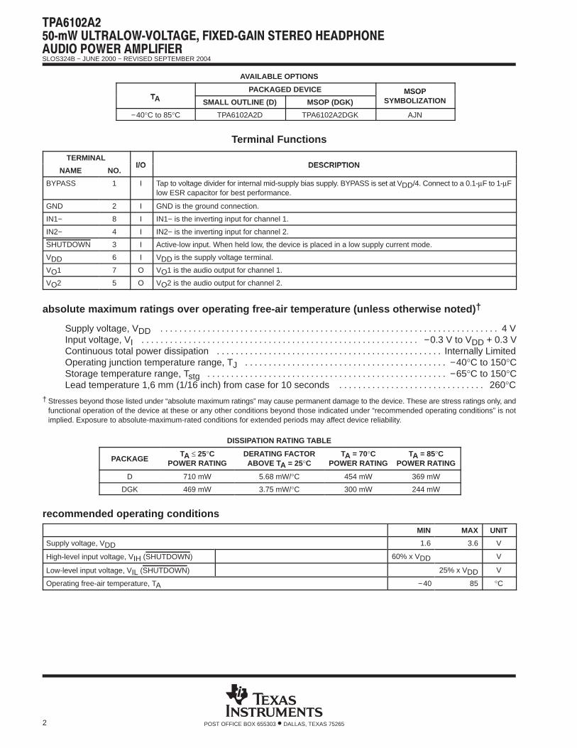
Terminal Functions
TERMINALI/O DESCRIPTION
NAME NO.I/O DESCRIPTION
BYPASS 1 I Tap to voltage divider for internal mid-supply bias supply. BYPASS is set at VDD/4. Connect to a 0.1-µF to 1-µFlow ESR capacitor for best performance.
GND 2 I GND is the ground connection.
IN1− 8 I IN1− is the inverting input for channel 1.
IN2− 4 I IN2− is the inverting input for channel 2.
SHUTDOWN 3 I Active-low input. When held low, the device is placed in a low supply current mode.
VDD 6 I VDD is the supply voltage terminal.
VO1 7 O VO1 is the audio output for channel 1.
VO2 5 O VO2 is the audio output for channel 2.
absolute maximum ratings over operating free-air temperature (unless otherwise noted) †
Supply voltage, VDD 4 V. . . . . . . . . . . . . . . . . . . . . . . . . . . . . . . . . . . . . . . . . . . . . . . . . . . . . . . . . . . . . . . . . . . . . . . . Input voltage, VI −0.3 V to VDD + 0.3 V. . . . . . . . . . . . . . . . . . . . . . . . . . . . . . . . . . . . . . . . . . . . . . . . . . . . . . . . . . . Continuous total power dissipation Internally Limited. . . . . . . . . . . . . . . . . . . . . . . . . . . . . . . . . . . . . . . . . . . . . . . . Operating junction temperature range, TJ −40°C to 150°C. . . . . . . . . . . . . . . . . . . . . . . . . . . . . . . . . . . . . . . . . . . Storage temperature range, Tstg −65°C to 150°C. . . . . . . . . . . . . . . . . . . . . . . . . . . . . . . . . . . . . . . . . . . . . . . . . . . Lead temperature 1,6 mm (1/16 inch) from case for 10 seconds 260°C. . . . . . . . . . . . . . . . . . . . . . . . . . . . . . .
† Stresses beyond those listed under “absolute maximum ratings” may cause permanent damage to the device. These are stress ratings only, andfunctional operation of the device at these or any other conditions beyond those indicated under “recommended operating conditions” is notimplied. Exposure to absolute-maximum-rated conditions for extended periods may affect device reliability.
DISSIPATION RATING TABLE
PACKAGETA ≤ 25°C
POWER RATINGDERATING FACTORABOVE TA = 25°C
TA = 70°CPOWER RATING
TA = 85°CPOWER RATING
D 710 mW 5.68 mW/°C 454 mW 369 mW
DGK 469 mW 3.75 mW/°C 300 mW 244 mW
recommended operating conditions
MIN MAX UNITÁÁÁÁÁÁÁÁÁÁÁÁÁÁÁÁÁÁÁÁÁÁÁÁÁÁÁÁÁÁÁÁÁÁÁÁÁÁÁÁÁÁÁÁÁÁÁÁÁÁSupply voltage, VDD
ÁÁÁÁÁÁÁÁ1.6
ÁÁÁÁÁÁÁÁÁÁ3.6
ÁÁÁÁÁÁVÁÁÁÁÁÁÁÁÁÁÁÁÁ
ÁÁÁÁÁÁÁÁÁÁÁÁÁHigh-level input voltage, VIH (SHUTDOWN)ÁÁÁÁÁÁÁÁÁÁÁÁÁÁÁÁÁÁÁÁÁÁÁÁÁÁ
ÁÁÁÁÁÁÁÁ60% x VDD
ÁÁÁÁÁÁÁÁÁÁ
ÁÁÁÁÁÁVÁÁÁÁÁÁÁÁÁÁÁÁÁ
ÁÁÁÁÁÁÁÁÁÁÁÁÁLow-level input voltage, VIL (SHUTDOWN)
ÁÁÁÁÁÁÁÁÁÁÁÁÁÁÁÁÁÁÁÁÁÁÁÁÁÁ
ÁÁÁÁÁÁÁÁ
ÁÁÁÁÁÁÁÁÁÁ
25% x VDDÁÁÁÁÁÁ
VÁÁÁÁÁÁÁÁÁÁÁÁÁÁÁÁÁÁÁÁÁÁÁÁÁÁÁÁÁÁÁÁÁÁÁÁÁÁÁÁÁÁÁÁÁÁÁÁÁÁ
Operating free-air temperature, TAÁÁÁÁÁÁÁÁ
−40ÁÁÁÁÁÁÁÁÁÁ
85ÁÁÁÁÁÁ
°C
SLOS324B − JUNE 2000 − REVISED SEPTEMBER 2004
3POST OFFICE BOX 655303 • DALLAS, TEXAS 75265
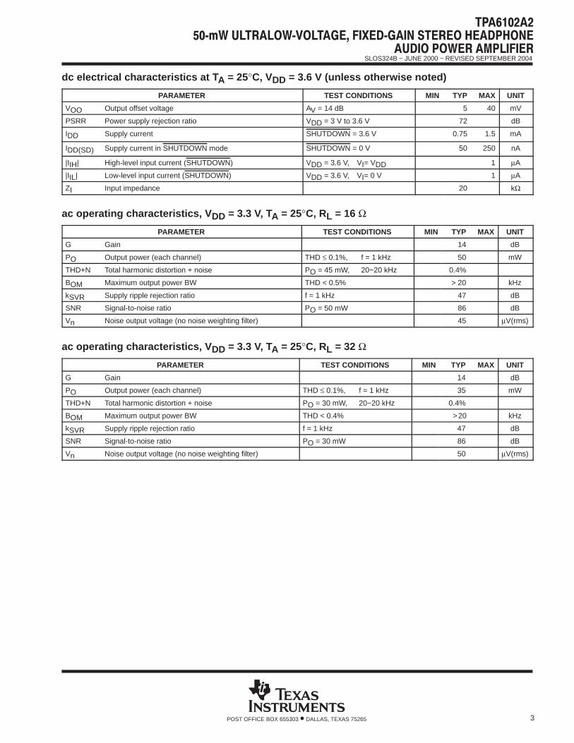
dc electrical characteristics at T A = 25°C, VDD = 3.6 V (unless otherwise noted)
PARAMETER TEST CONDITIONS MIN TYP MAX UNIT
VOO Output offset voltage AV = 14 dB 5 40 mV
PSRR Power supply rejection ratio VDD = 3 V to 3.6 V 72 dB
IDD Supply current SHUTDOWN = 3.6 V 0.75 1.5 mA
IDD(SD) Supply current in SHUTDOWN mode SHUTDOWN = 0 V 50 250 nA
|IIH| High-level input current (SHUTDOWN) VDD = 3.6 V, VI= VDD 1 µA
|IIL| Low-level input current (SHUTDOWN) VDD = 3.6 V, VI= 0 V 1 µA
ZI Input impedance 20 kΩ
ac operating characteristics, V DD = 3.3 V, TA = 25°C, RL = 16 Ω
PARAMETER TEST CONDITIONS MIN TYP MAX UNIT
G Gain 14 dB
PO Output power (each channel) THD ≤ 0.1%, f = 1 kHz 50 mW
THD+N Total harmonic distortion + noise PO = 45 mW, 20−20 kHz 0.4%
BOM Maximum output power BW THD < 0.5% > 20 kHz
kSVR Supply ripple rejection ratio f = 1 kHz 47 dB
SNR Signal-to-noise ratio PO = 50 mW 86 dB
Vn Noise output voltage (no noise weighting filter) 45 µV(rms)
ac operating characteristics, V DD = 3.3 V, TA = 25°C, RL = 32 Ω
PARAMETER TEST CONDITIONS MIN TYP MAX UNIT
G Gain 14 dB
PO Output power (each channel) THD ≤ 0.1%, f = 1 kHz 35 mW
THD+N Total harmonic distortion + noise PO = 30 mW, 20−20 kHz 0.4%
BOM Maximum output power BW THD < 0.4% >20 kHz
kSVR Supply ripple rejection ratio f = 1 kHz 47 dB
SNR Signal-to-noise ratio PO = 30 mW 86 dB
Vn Noise output voltage (no noise weighting filter) 50 µV(rms)
SLOS324B − JUNE 2000 − REVISED SEPTEMBER 2004
4 POST OFFICE BOX 655303 • DALLAS, TEXAS 75265
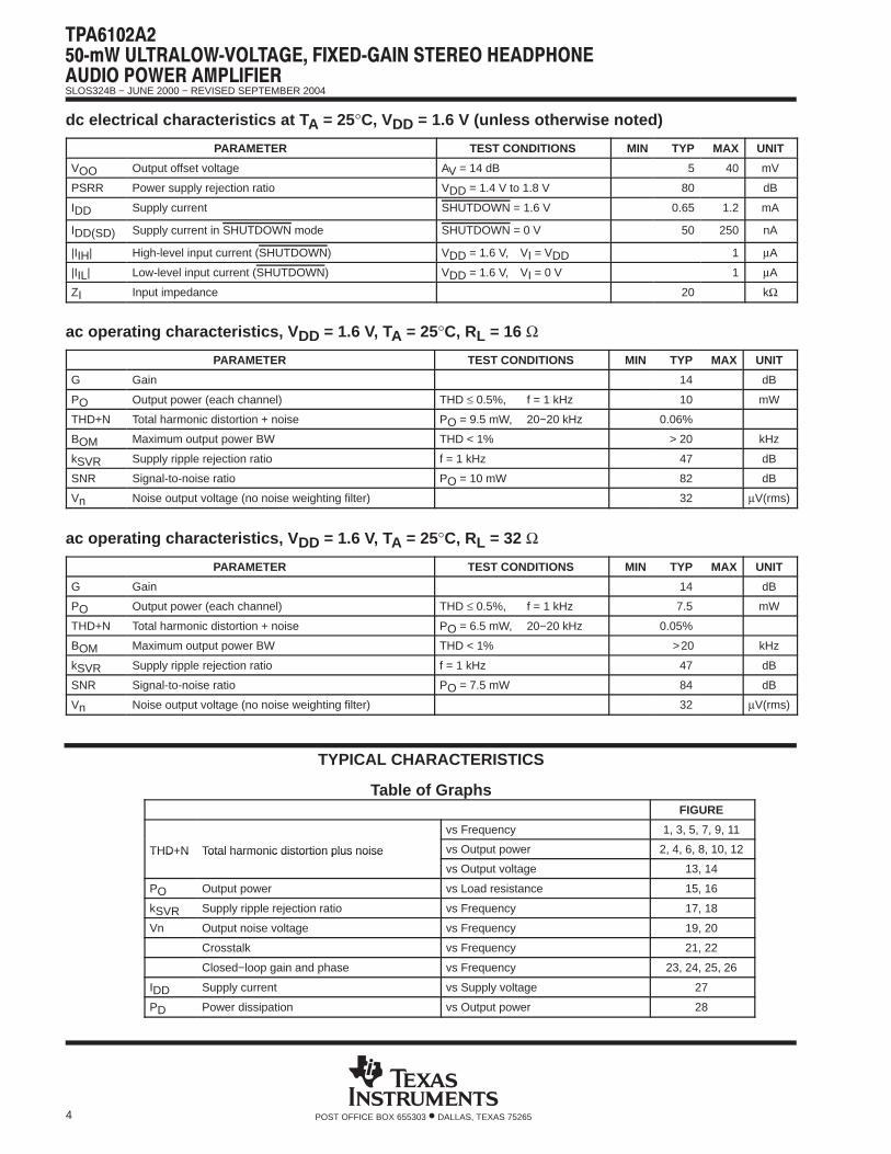
dc electrical characteristics at T A = 25°C, VDD = 1.6 V (unless otherwise noted)
PARAMETER TEST CONDITIONS MIN TYP MAX UNIT
VOO Output offset voltage AV = 14 dB 5 40 mV
PSRR Power supply rejection ratio VDD = 1.4 V to 1.8 V 80 dB
IDD Supply current SHUTDOWN = 1.6 V 0.65 1.2 mA
IDD(SD) Supply current in SHUTDOWN mode SHUTDOWN = 0 V 50 250 nA
|IIH| High-level input current (SHUTDOWN) VDD = 1.6 V, VI = VDD 1 µA
|IIL| Low-level input current (SHUTDOWN) VDD = 1.6 V, VI = 0 V 1 µA
ZI Input impedance 20 kΩ
ac operating characteristics, V DD = 1.6 V, TA = 25°C, RL = 16 Ω
PARAMETER TEST CONDITIONS MIN TYP MAX UNIT
G Gain 14 dB
PO Output power (each channel) THD ≤ 0.5%, f = 1 kHz 10 mW
THD+N Total harmonic distortion + noise PO = 9.5 mW, 20−20 kHz 0.06%
BOM Maximum output power BW THD < 1% > 20 kHz
kSVR Supply ripple rejection ratio f = 1 kHz 47 dB
SNR Signal-to-noise ratio PO = 10 mW 82 dB
Vn Noise output voltage (no noise weighting filter) 32 µV(rms)
ac operating characteristics, V DD = 1.6 V, TA = 25°C, RL = 32 Ω
PARAMETER TEST CONDITIONS MIN TYP MAX UNIT
G Gain 14 dB
PO Output power (each channel) THD ≤ 0.5%, f = 1 kHz 7.5 mW
THD+N Total harmonic distortion + noise PO = 6.5 mW, 20−20 kHz 0.05%
BOM Maximum output power BW THD < 1% >20 kHz
kSVR Supply ripple rejection ratio f = 1 kHz 47 dB
SNR Signal-to-noise ratio PO = 7.5 mW 84 dB
Vn Noise output voltage (no noise weighting filter) 32 µV(rms)
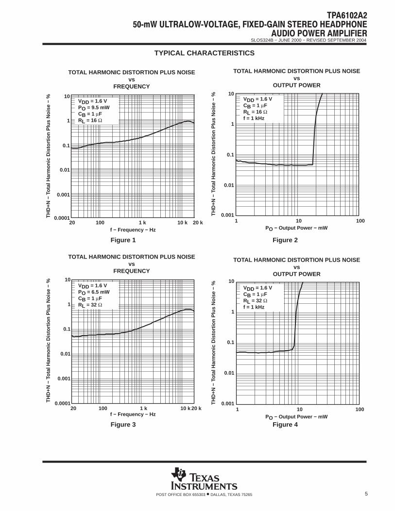
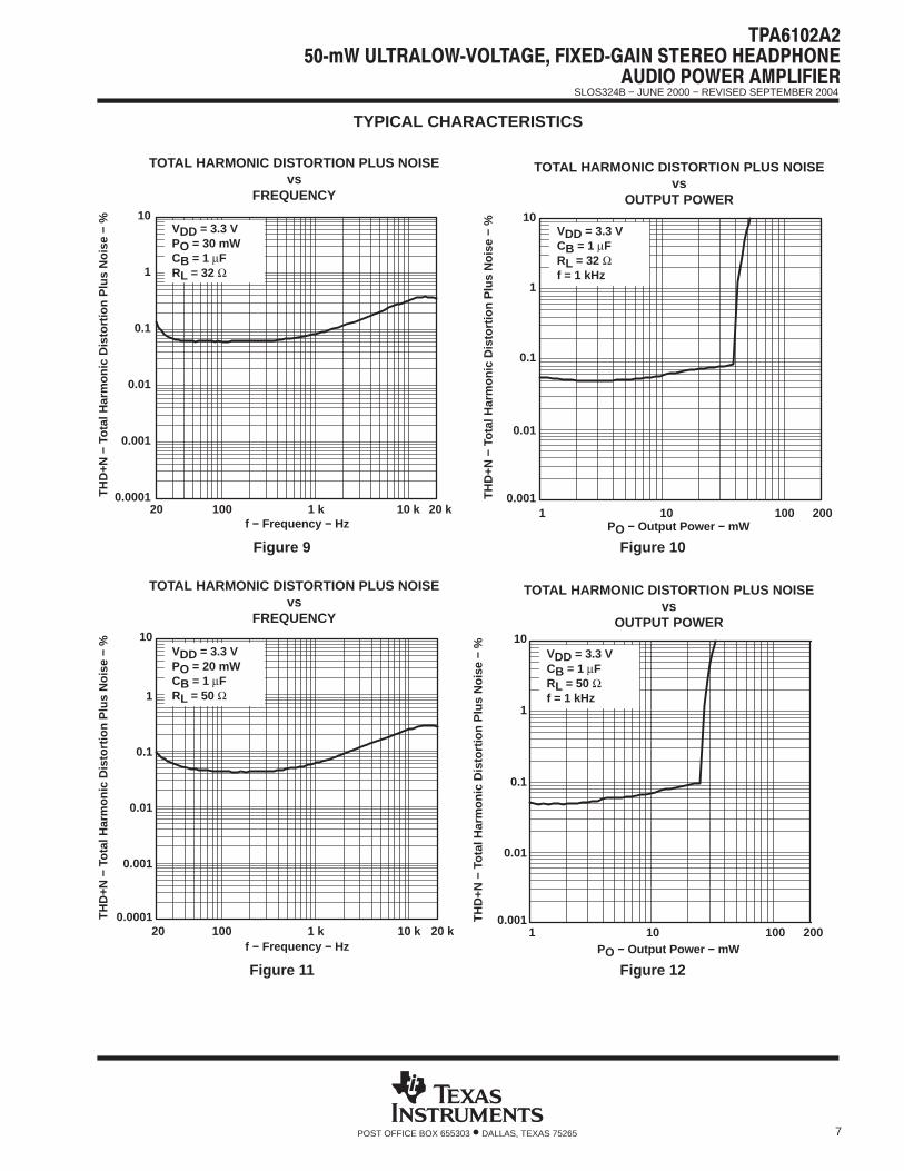
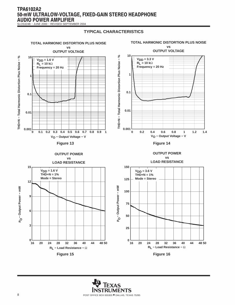
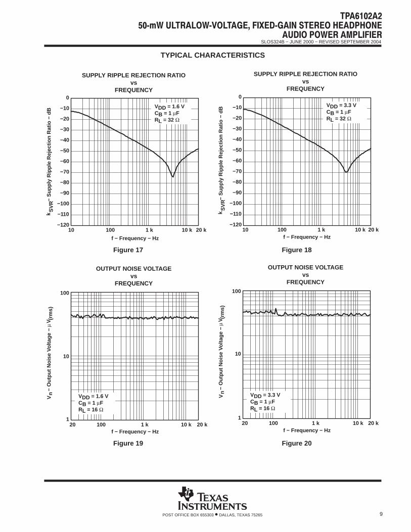
TYPICAL CHARACTERISTICS
Table of GraphsFIGURE
vs Frequency 1, 3, 5, 7, 9, 11
THD+N Total harmonic distortion plus noise vs Output power 2, 4, 6, 8, 10, 12THD+N Total harmonic distortion plus noise
vs Output voltage 13, 14
PO Output power vs Load resistance 15, 16
kSVR Supply ripple rejection ratio vs Frequency 17, 18
Vn Output noise voltage vs Frequency 19, 20
Crosstalk vs Frequency 21, 22
Closed−loop gain and phase vs Frequency 23, 24, 25, 26
IDD Supply current vs Supply voltage 27
PD Power dissipation vs Output power 28
SLOS324B − JUNE 2000 − REVISED SEPTEMBER 2004
5POST OFFICE BOX 655303 • DALLAS, TEXAS 75265
TYPICAL CHARACTERISTICS
Figure 1
0.0001
10
0.001
0.01
0.1
1
20 20 k100 1 k 10 k
TH
D+N
− T
otal
Har
mon
ic D
isto
rtio
n P
lus
Noi
se −
%
f − Frequency − Hz
TOTAL HARMONIC DISTORTION PLUS NOISEvs
FREQUENCY
VDD = 1.6 VPO = 9.5 mWCB = 1 µFRL = 16 Ω
Figure 2
1
0.001
10
0.01
0.1
1 10010
TH
D+N
− T
otal
Har
mon
ic D
isto
rtio
n P
lus
Noi
se −
%
VDD = 1.6 VCB = 1 µFRL = 16 Ωf = 1 kHz
TOTAL HARMONIC DISTORTION PLUS NOISEvs
OUTPUT POWER
PO − Output Power − mW
Figure 3
0.0001
10
0.001
0.01
0.1
1
20 20 k100 1 k 10 k
TH
D+N
− T
otal
Har
mon
ic D
isto
rtio
n P
lus
Noi
se −
%
f − Frequency − Hz
TOTAL HARMONIC DISTORTION PLUS NOISEvs
FREQUENCY
VDD = 1.6 VPO = 6.5 mWCB = 1 µFRL = 32 Ω
Figure 4
0.001
10
0.01
0.1
1
1 10010
TH
D+N
− T
otal
Har
mon
ic D
isto
rtio
n P
lus
Noi
se −
%
VDD = 1.6 VCB = 1 µFRL = 32 Ωf = 1 kHz
TOTAL HARMONIC DISTORTION PLUS NOISEvs
OUTPUT POWER
PO − Output Power − mW

SLOS324B − JUNE 2000 − REVISED SEPTEMBER 2004
6 POST OFFICE BOX 655303 • DALLAS, TEXAS 75265
TYPICAL CHARACTERISTICS
Figure 5
10 k0.0001
10
0.001
0.01
0.1
1
20 20 k100 1 k
TH
D+N
− T
otal
Har
mon
ic D
isto
rtio
n P
lus
Noi
se −
%
f − Frequency − Hz
TOTAL HARMONIC DISTORTION PLUS NOISEvs
FREQUENCY
VDD = 1.6 VPO = 4.5 mWCB = 1 µFRL = 50 Ω
Figure 6
0.001
10
0.01
0.1
1
1 10010
TH
D+N
− T
otal
Har
mon
ic D
isto
rtio
n P
lus
Noi
se −
%
VDD = 1.6 VCB = 1 µFRL = 50 Ωf = 1 kHz
TOTAL HARMONIC DISTORTION PLUS NOISEvs
OUTPUT POWER
PO − Output Power − mW
Figure 7
0.0001
10
0.001
0.01
0.1
1
20 20 k100 1 k 10 k
TH
D+N
− T
otal
Har
mon
ic D
isto
rtio
n P
lus
Noi
se −
%
f − Frequency − Hz
TOTAL HARMONIC DISTORTION PLUS NOISEvs
FREQUENCY
VDD = 3.3 VPO = 45 mWCB = 1 µFRL = 16 Ω
Figure 8
0.0001
10
0.001
0.01
0.1
1
20 20 k100 1 k 10 k
TH
D+N
− T
otal
Har
mon
ic D
isto
rtio
n P
lus
Noi
se −
%
VDD = 3.3 VCB = 1 µFRL = 16 Ωf = 1 kHz
TOTAL HARMONIC DISTORTION PLUS NOISEvs
OUTPUT POWER
PO − Output Power − mW
SLOS324B − JUNE 2000 − REVISED SEPTEMBER 2004
7POST OFFICE BOX 655303 • DALLAS, TEXAS 75265
TYPICAL CHARACTERISTICS
Figure 9
0.0001
10
0.001
0.01
0.1
1
20 20 k100 1 k 10 k
TH
D+N
− T
otal
Har
mon
ic D
isto
rtio
n P
lus
Noi
se −
%
f − Frequency − Hz
TOTAL HARMONIC DISTORTION PLUS NOISEvs
FREQUENCY
VDD = 3.3 VPO = 30 mWCB = 1 µFRL = 32 Ω
Figure 10
0.001
10
0.01
0.1
1
1 20010 100
TH
D+N
− T
otal
Har
mon
ic D
isto
rtio
n P
lus
Noi
se −
%
VDD = 3.3 VCB = 1 µFRL = 32 Ωf = 1 kHz
TOTAL HARMONIC DISTORTION PLUS NOISEvs
OUTPUT POWER
PO − Output Power − mW
Figure 11
0.0001
10
0.001
0.01
0.1
1
20 20 k100 1 k 10 k
TH
D+N
− T
otal
Har
mon
ic D
isto
rtio
n P
lus
Noi
se −
%
f − Frequency − Hz
TOTAL HARMONIC DISTORTION PLUS NOISEvs
FREQUENCY
VDD = 3.3 VPO = 20 mWCB = 1 µFRL = 50 Ω
Figure 12
0.001
10
0.01
0.1
1
1 20010 100
TH
D+N
− T
otal
Har
mon
ic D
isto
rtio
n P
lus
Noi
se −
%
VDD = 3.3 VCB = 1 µFRL = 50 Ωf = 1 kHz
TOTAL HARMONIC DISTORTION PLUS NOISEvs
OUTPUT POWER
PO − Output Power − mW
SLOS324B − JUNE 2000 − REVISED SEPTEMBER 2004
8 POST OFFICE BOX 655303 • DALLAS, TEXAS 75265
TYPICAL CHARACTERISTICS
Figure 13
0.001
0.01
0.1
1
10
0 0.1 0.2 0.3 0.4 0.5 0.6 0.7 0.8 0.9 1
TH
D+N
− T
otal
Har
mon
ic D
isto
rtio
n P
lus
Noi
se −
%
VDD = 1.6 VRL = 10 kΩFrequency = 20 Hz
TOTAL HARMONIC DISTORTION PLUS NOISEvs
OUTPUT VOLTAGE
VO − Output Voltage − V
Figure 14
0.001
0.01
0.1
1
10
0 0.2 0.4 0.6 0.8 1 1.2 1.4
TH
D+N
− T
otal
Har
mon
ic D
isto
rtio
n P
lus
Noi
se −
%
VDD = 3.3 VRL = 10 kΩFrequency = 20 Hz
TOTAL HARMONIC DISTORTION PLUS NOISEvs
OUTPUT VOLTAGE
VO − Output Voltage − V
Figure 15
0
3
6
9
12
15
16 20 24 28 32 36 40 44 48 50
− O
utpu
t Pow
er −
mW
OUTPUT POWERvs
LOAD RESISTANCE
PO
VDD = 1.6 VTHD+N = 1%Mode = Stereo
RL − Load Resistance − Ω
Figure 16
0
25
50
75
100
125
150
16 20 24 28 32 36 40 44 48 50
− O
utpu
t Pow
er −
mW
OUTPUT POWERvs
LOAD RESISTANCE
PO
VDD = 3.6 VTHD+N = 1%Mode = Stereo
RL − Load Resistance − Ω
SLOS324B − JUNE 2000 − REVISED SEPTEMBER 2004
9POST OFFICE BOX 655303 • DALLAS, TEXAS 75265
TYPICAL CHARACTERISTICS
Figure 17
−120
0
−110
−100
−90
−80
−70
−60
−50
−40
−30
−20
−10
10 20 k100 1 k 10 k
− S
uppl
y R
ippl
e R
ejec
tion
Rat
io −
dB
f − Frequency − Hz
SUPPLY RIPPLE REJECTION RATIOvs
FREQUENCY
VDD = 1.6 VCB = 1 µFRL = 32 Ω
kS
VR
Figure 18
−120
0
−110
−100
−90
−80
−70
−60
−50
−40
−30
−20
−10
10 20 k100 1 k 10 k
− S
uppl
y R
ippl
e R
ejec
tion
Rat
io −
dB
f − Frequency − Hz
SUPPLY RIPPLE REJECTION RATIOvs
FREQUENCY
VDD = 3.3 VCB = 1 µFRL = 32 Ω
kS
VR
Figure 19
1
100
10
20 20 k100 1 k 10 k
− O
utpu
t Noi
se V
olta
ge −
f − Frequency − Hz
OUTPUT NOISE VOLTAGEvs
FREQUENCY
VDD = 1.6 VCB = 1 µFRL = 16 Ω
Vn
Vµ
(rm
s)
Figure 20
1
100
10
20 20 k100 1 k 10 k
− O
utpu
t Noi
se V
olta
ge −
f − Frequency − Hz
OUTPUT NOISE VOLTAGEvs
FREQUENCY
VDD = 3.3 VCB = 1 µFRL = 16 Ω
Vn
Vµ
(rm
s)

SLOS324B − JUNE 2000 − REVISED SEPTEMBER 2004
10 POST OFFICE BOX 655303 • DALLAS, TEXAS 75265
TYPICAL CHARACTERISTICS
Figure 21
−140
0
−130
−120
−110
−100
−90
−80
−70
−60
−50
−40
−30
−20
−10
20 20 k100 1 k 10 k
Cro
ssta
lk −
dB
f − Frequency − Hz
CROSSTALKvs
FREQUENCY
VDD = 1.6 VPO = 4.5 mWRL = 50 Ω
Figure 22
−140
0
−130
−120
−110
−100
−90
−80
−70
−60
−50
−40
−30
−20
−10
20 20 k100 1 k 10 k
Cro
ssta
lk −
dB
f − Frequency − Hz
CROSSTALKvs
FREQUENCY
VDD = 3.3 VPO = 20 mWRL = 50 Ω
−60
−50
−40
−30
−20
−10
0
10
20
30
40
10 100 1 k 10 k 100 k 1 M 10 M 100 M
Phase
Gain
VDD = 1.6 VRL = 16 ΩTA = 25°C
Clo
sed-
Loop
Gai
n −
dB
f − Frequency − Hz
CLOSED-LOOP GAIN AND PHASEvs
FREQUENCYP
hase
Figure 23
180°
−180°
60°
−60°
150°
120°
30°
−30°
−120°
−150°
−90°
0°
90°
SLOS324B − JUNE 2000 − REVISED SEPTEMBER 2004
11POST OFFICE BOX 655303 • DALLAS, TEXAS 75265
TYPICAL CHARACTERISTICS
−60
−50
−40
−30
−20
−10
0
10
20
30
40
10 100 1 k 10 k 100 k 1 M 10 M 100 M
Phase
Gain
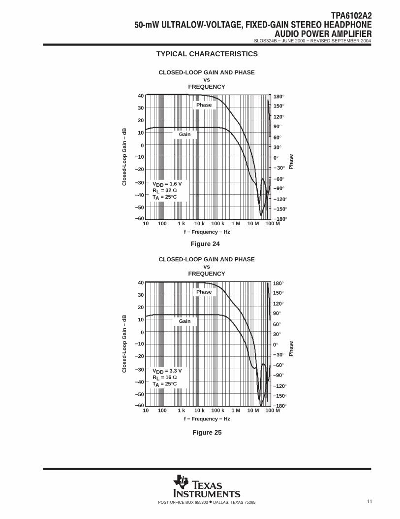
VDD = 1.6 VRL = 32 ΩTA = 25°C
Clo
sed-
Loop
Gai
n −
dB
f − Frequency − Hz
CLOSED-LOOP GAIN AND PHASEvs
FREQUENCY
Pha
se
Figure 24
180°
−180°
60°
−60°
150°
120°
30°
−30°
−120°
−150°
−90°
0°
90°
−60
−50
−40
−30
−20
−10
0
10
20
30
40
10 100 1 k 10 k 100 k 1 M 10 M 100 M
Phase
Gain
VDD = 3.3 VRL = 16 ΩTA = 25°C
Clo
sed-
Loop
Gai
n −
dB
f − Frequency − Hz
CLOSED-LOOP GAIN AND PHASEvs
FREQUENCY
Pha
se
Figure 25
180°
−180°
60°
−60°
150°
120°
30°
−30°
−120°
−150°
−90°
0°
90°
SLOS324B − JUNE 2000 − REVISED SEPTEMBER 2004
12 POST OFFICE BOX 655303 • DALLAS, TEXAS 75265
TYPICAL CHARACTERISTICS
−60
−50
−40
−30
−20
−10
0
10
20
30
40
10 100 1 k 10 k 100 k 1 M 10 M 100 M
Phase
Gain
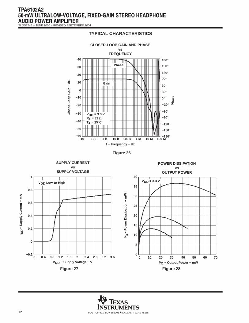
VDD = 3.3 VRL = 32 ΩTA = 25°C
Clo
sed-
Loop
Gai
n −
dB
f − Frequency − Hz
CLOSED-LOOP GAIN AND PHASEvs
FREQUENCY
Pha
se
Figure 26
180°
−180°
60°
−60°
150°
120°
30°
−30°
−120°
−150°
−90°
0°
90°
Figure 27
−0.2
0
0.2
0.4
0.6
0.8
1
0 0.4 0.8 1.2 1.6 2 2.4 2.8 3.2 3.6
− S
uppl
y C
urre
nt −
mA
SUPPLY CURRENTvs
SUPPLY VOLTAGE
I DD
VDD − Supply Voltage − V
VDD Low-to-High
Figure 28
5
10
15
20
25
30
35
40
00 10 20 40
− P
ower
Dis
sipa
tion
− m
W
POWER DISSIPATIONvs
OUTPUT POWER
50 7030 60
PO − Output Power − mW
PD
VDD = 3.3 V

SLOS324B − JUNE 2000 − REVISED SEPTEMBER 2004
13POST OFFICE BOX 655303 • DALLAS, TEXAS 75265
APPLICATION INFORMATION
input capacitor, C I
In the typical application, an input capacitor (CI) is required to allow the amplifier to bias the input signal to theproper dc level for optimum operation. In this case, CI and RI form a high-pass filter with the corner frequencydetermined in equation 1. RI is set internally and is fixed at 20 kΩ.
(1)fc 12RICI
The value of CI is important to consider, as it directly affects the bass (low frequency) performance of the circuit.Consider the example where the specification calls for a flat bass response down to 20 Hz. Equation 1 isreconfigured as equation 2.
(2)CI 12RIfc
In this example, CI is 0.40 µF, so one would likely choose a value in the range of 0.47 µF to 1 µF. A furtherconsideration for this capacitor is the leakage path from the input source through the input network (RI, CI) andthe feedback resistor (RF) to the load. This leakage current creates a dc offset voltage at the input to the amplifierthat reduces useful headroom. For this reason a low-leakage tantalum or ceramic capacitor is the best choice.When polarized capacitors are used, the positive side of the capacitor should face the amplifier input in mostapplications, as the dc level there is held at VDD/4, which is likely higher than the source dc level. It is importantto confirm the capacitor polarity in the application.
power supply decoupling, C S
The TPA6102A2 is a high-performance CMOS audio amplifier that requires adequate power supply decouplingto ensure that the output total harmonic distortion (THD) is as low as possible. Power supply decoupling alsoprevents oscillations for long lead lengths between the amplifier and the speaker. The optimum decoupling isachieved by using two capacitors of different types that target different types of noise on the power supply leads.For higher frequency transients, spikes, or digital hash on the line, a good low equivalent-series-resistance(ESR) ceramic capacitor, typically 0.1 µF, placed as close as possible to the device VDD lead, works best. Forfiltering lower-frequency noise signals, a larger aluminum electrolytic capacitor of 10 µF or greater placed nearthe power amplifier is recommended.
midrail bypass capacitor, C B
The midrail bypass capacitor (CB) serves several important functions. During start-up, CB determines the rateat which the amplifier starts up. This helps to push the start-up pop noise into the subaudible range (so low itcan not be heard). The second function is to reduce noise produced by the power supply caused by couplinginto the output drive signal. This noise is from the midrail generation circuit internal to the amplifier. The capacitoris fed from a 55-kΩ source inside the amplifier. To keep the start-up pop as low as possible, the relationshipshown in equation 3 should be maintained.
(3)1
CB 55 kΩ 1CIRI
As an example, consider a circuit where CB is 1 µF, CI is 1 µF, and RI is 20 kΩ. Inserting these values into theequation 3 results in: 18.18 ≤ 50 which satisfies the rule. Bypass capacitor (CB) with values of 0.47-µF to 1-µFceramic or tantalum low-ESR capacitors are recommended for the best THD and noise performance.

SLOS324B − JUNE 2000 − REVISED SEPTEMBER 2004
14 POST OFFICE BOX 655303 • DALLAS, TEXAS 75265
APPLICATION INFORMATION
output coupling capacitor, C C
In the typical single-supply single-ended (SE) configuration, an output coupling capacitor (CC) is required toblock the dc bias at the output of the amplifier, thus preventing dc currents in the load. As with the input couplingcapacitor, the output coupling capacitor and impedance of the load form a high-pass filter governed byequation 4.
(4)fc 12RLCC
The main disadvantage, from a performance standpoint, is that the typically small load impedances drive thelow-frequency corner higher. Large values of CC are required to pass low-frequencies into the load. Considerthe example where a CC of 68 µF is chosen and loads vary from 32 Ω to 47 kΩ. Table 1 summarizes thefrequency response characteristics of each configuration.
Table 1. Common-Load Impedances vs Low-Frequency Output Characteristics in SE Mode
RL CC Lowest Frequency
32 Ω 68 µF 73 Hz
10,000 Ω 68 µF 0.23 Hz
47,000 Ω 68 µF 0.05 Hz
As Table 1 indicates, headphone response is adequate and drive into line level inputs (a home stereo forexample) is very good.
The output-coupling capacitor required in single-supply SE mode also places additional constraints on theselection of other components in the amplifier circuit. With the rules described earlier still valid, add the followingrelationship:
(5)1
CB 55 kΩ 1CIRI
1
RLCC
using low-ESR capacitors
Low-ESR capacitors are recommended throughout this application. A real capacitor can be modeled simply asa resistor in series with an ideal capacitor. The voltage drop across this resistor minimizes the beneficial effectsof the capacitor in the circuit. The lower the equivalent value of this resistance, the more the real capacitorbehaves like an ideal capacitor.
3.3-V versus 1.6-V operation
The TPA6102A2 was designed for operation over a supply range of 1.6 V to 3.6 V. There are no specialconsiderations for 1.6-V versus 3.3-V operation as far as supply bypassing, gain setting, or stability. Supplycurrent is slightly reduced from 0.75 mA (typical) to 0.65 mA (typical). The most important consideration is thatof output power. Each amplifier can produce a maxium output voltage swing within a few hundred millivolts ofthe rails with a 10-kΩ load. However, this voltage swing decreases as the load resistance decreases and therDS(on) as the output stage transistors becomes more significant. For example, for a 32-Ω load, the maximumpeak output voltage with VDD = 1.6 V is approximately 0.7 V with no clipping distortion. This reduced voltageswing effectively reduces the maximum undistorted output power.
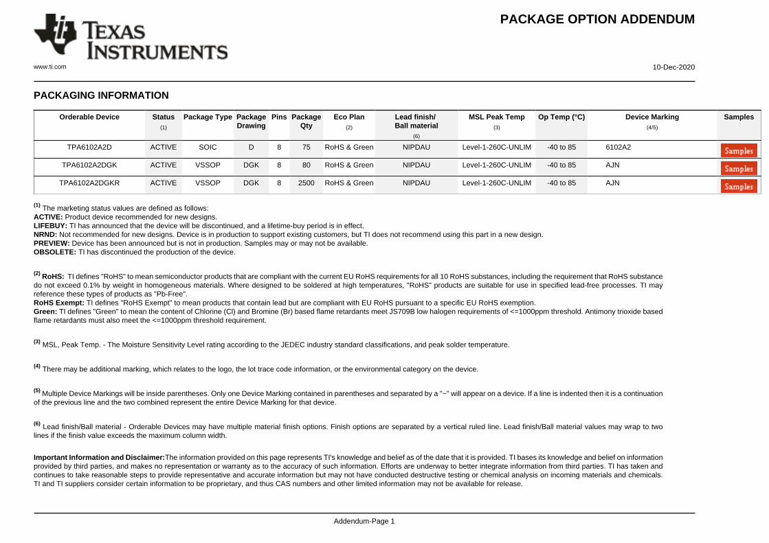
PACKAGE OPTION ADDENDUM
www.ti.com 10-Dec-2020
Addendum-Page 1
PACKAGING INFORMATION
Orderable Device Status(1)
Package Type PackageDrawing
Pins PackageQty
Eco Plan(2)
Lead finish/Ball material
(6)
MSL Peak Temp(3)
Op Temp (°C) Device Marking(4/5)
Samples
TPA6102A2D ACTIVE SOIC D 8 75 RoHS & Green NIPDAU Level-1-260C-UNLIM -40 to 85 6102A2
TPA6102A2DGK ACTIVE VSSOP DGK 8 80 RoHS & Green NIPDAU Level-1-260C-UNLIM -40 to 85 AJN
TPA6102A2DGKR ACTIVE VSSOP DGK 8 2500 RoHS & Green NIPDAU Level-1-260C-UNLIM -40 to 85 AJN
(1) The marketing status values are defined as follows:ACTIVE: Product device recommended for new designs.LIFEBUY: TI has announced that the device will be discontinued, and a lifetime-buy period is in effect.NRND: Not recommended for new designs. Device is in production to support existing customers, but TI does not recommend using this part in a new design.PREVIEW: Device has been announced but is not in production. Samples may or may not be available.OBSOLETE: TI has discontinued the production of the device.
(2) RoHS: TI defines "RoHS" to mean semiconductor products that are compliant with the current EU RoHS requirements for all 10 RoHS substances, including the requirement that RoHS substancedo not exceed 0.1% by weight in homogeneous materials. Where designed to be soldered at high temperatures, "RoHS" products are suitable for use in specified lead-free processes. TI mayreference these types of products as "Pb-Free".RoHS Exempt: TI defines "RoHS Exempt" to mean products that contain lead but are compliant with EU RoHS pursuant to a specific EU RoHS exemption.Green: TI defines "Green" to mean the content of Chlorine (Cl) and Bromine (Br) based flame retardants meet JS709B low halogen requirements of <=1000ppm threshold. Antimony trioxide basedflame retardants must also meet the <=1000ppm threshold requirement.
(3) MSL, Peak Temp. - The Moisture Sensitivity Level rating according to the JEDEC industry standard classifications, and peak solder temperature.
(4) There may be additional marking, which relates to the logo, the lot trace code information, or the environmental category on the device.
(5) Multiple Device Markings will be inside parentheses. Only one Device Marking contained in parentheses and separated by a "~" will appear on a device. If a line is indented then it is a continuationof the previous line and the two combined represent the entire Device Marking for that device.
(6) Lead finish/Ball material - Orderable Devices may have multiple material finish options. Finish options are separated by a vertical ruled line. Lead finish/Ball material values may wrap to twolines if the finish value exceeds the maximum column width.
Important Information and Disclaimer:The information provided on this page represents TI's knowledge and belief as of the date that it is provided. TI bases its knowledge and belief on informationprovided by third parties, and makes no representation or warranty as to the accuracy of such information. Efforts are underway to better integrate information from third parties. TI has taken andcontinues to take reasonable steps to provide representative and accurate information but may not have conducted destructive testing or chemical analysis on incoming materials and chemicals.TI and TI suppliers consider certain information to be proprietary, and thus CAS numbers and other limited information may not be available for release.

PACKAGE OPTION ADDENDUM
www.ti.com 10-Dec-2020
Addendum-Page 2
In no event shall TI's liability arising out of such information exceed the total purchase price of the TI part(s) at issue in this document sold by TI to Customer on an annual basis.

TAPE AND REEL INFORMATION
*All dimensions are nominal
Device PackageType
PackageDrawing
Pins SPQ ReelDiameter
(mm)
ReelWidth
W1 (mm)
A0(mm)
B0(mm)
K0(mm)
P1(mm)
W(mm)
Pin1Quadrant
TPA6102A2DGKR VSSOP DGK 8 2500 330.0 12.4 5.3 3.4 1.4 8.0 12.0 Q1
PACKAGE MATERIALS INFORMATION
www.ti.com 5-Jan-2022
Pack Materials-Page 1
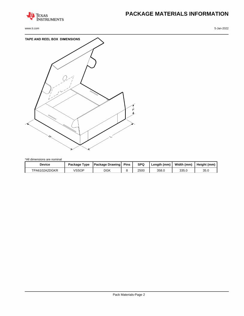
*All dimensions are nominal
Device Package Type Package Drawing Pins SPQ Length (mm) Width (mm) Height (mm)
TPA6102A2DGKR VSSOP DGK 8 2500 358.0 335.0 35.0
PACKAGE MATERIALS INFORMATION
www.ti.com 5-Jan-2022
Pack Materials-Page 2
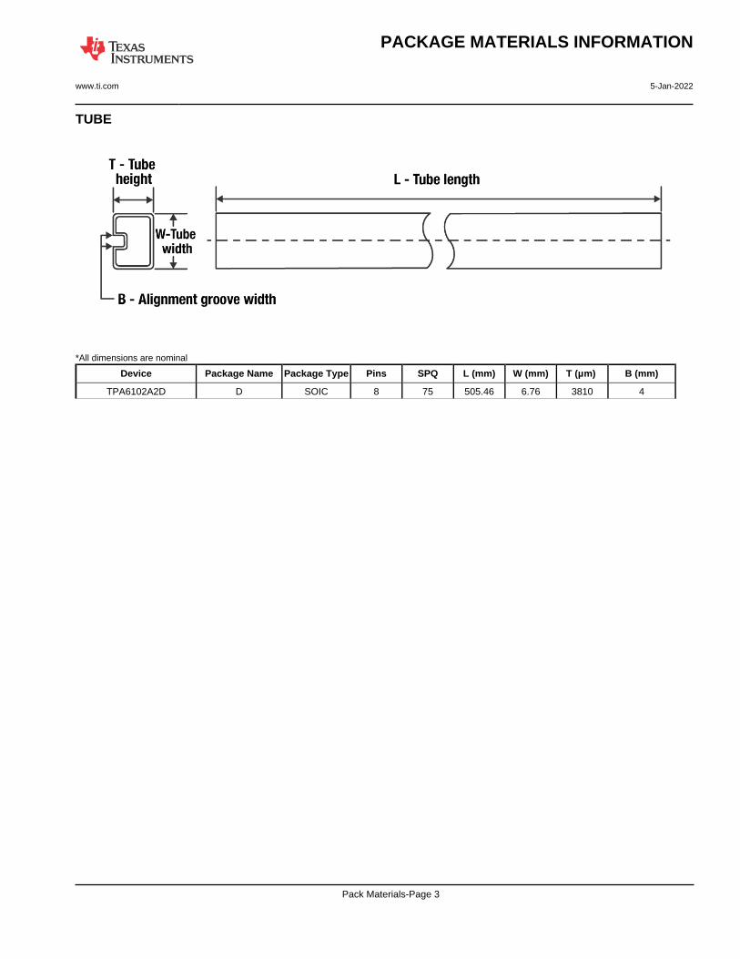
TUBE
*All dimensions are nominal
Device Package Name Package Type Pins SPQ L (mm) W (mm) T (µm) B (mm)
TPA6102A2D D SOIC 8 75 505.46 6.76 3810 4
PACKAGE MATERIALS INFORMATION
www.ti.com 5-Jan-2022
Pack Materials-Page 3

www.ti.com
PACKAGE OUTLINE
C
.228-.244 TYP[5.80-6.19]
.069 MAX[1.75]
6X .050[1.27]
8X .012-.020 [0.31-0.51]
2X.150[3.81]
.005-.010 TYP[0.13-0.25]
0 - 8 .004-.010[0.11-0.25]
.010[0.25]
.016-.050[0.41-1.27]
4X (0 -15 )
A
.189-.197[4.81-5.00]
NOTE 3
B .150-.157[3.81-3.98]
NOTE 4
4X (0 -15 )
(.041)[1.04]
SOIC - 1.75 mm max heightD0008ASMALL OUTLINE INTEGRATED CIRCUIT
4214825/C 02/2019
NOTES: 1. Linear dimensions are in inches [millimeters]. Dimensions in parenthesis are for reference only. Controlling dimensions are in inches. Dimensioning and tolerancing per ASME Y14.5M. 2. This drawing is subject to change without notice. 3. This dimension does not include mold flash, protrusions, or gate burrs. Mold flash, protrusions, or gate burrs shall not exceed .006 [0.15] per side. 4. This dimension does not include interlead flash.5. Reference JEDEC registration MS-012, variation AA.
18
.010 [0.25] C A B
54
PIN 1 ID AREA
SEATING PLANE
.004 [0.1] C
SEE DETAIL A
DETAIL ATYPICAL
SCALE 2.800

www.ti.com
EXAMPLE BOARD LAYOUT
.0028 MAX[0.07]ALL AROUND
.0028 MIN[0.07]ALL AROUND
(.213)[5.4]
6X (.050 )[1.27]
8X (.061 )[1.55]
8X (.024)[0.6]
(R.002 ) TYP[0.05]
SOIC - 1.75 mm max heightD0008ASMALL OUTLINE INTEGRATED CIRCUIT
4214825/C 02/2019
NOTES: (continued) 6. Publication IPC-7351 may have alternate designs. 7. Solder mask tolerances between and around signal pads can vary based on board fabrication site.
METALSOLDER MASKOPENING
NON SOLDER MASKDEFINED
SOLDER MASK DETAILS
EXPOSEDMETAL
OPENINGSOLDER MASK METAL UNDER
SOLDER MASK
SOLDER MASKDEFINED
EXPOSEDMETAL
LAND PATTERN EXAMPLEEXPOSED METAL SHOWN
SCALE:8X
SYMM
1
45
8
SEEDETAILS
SYMM
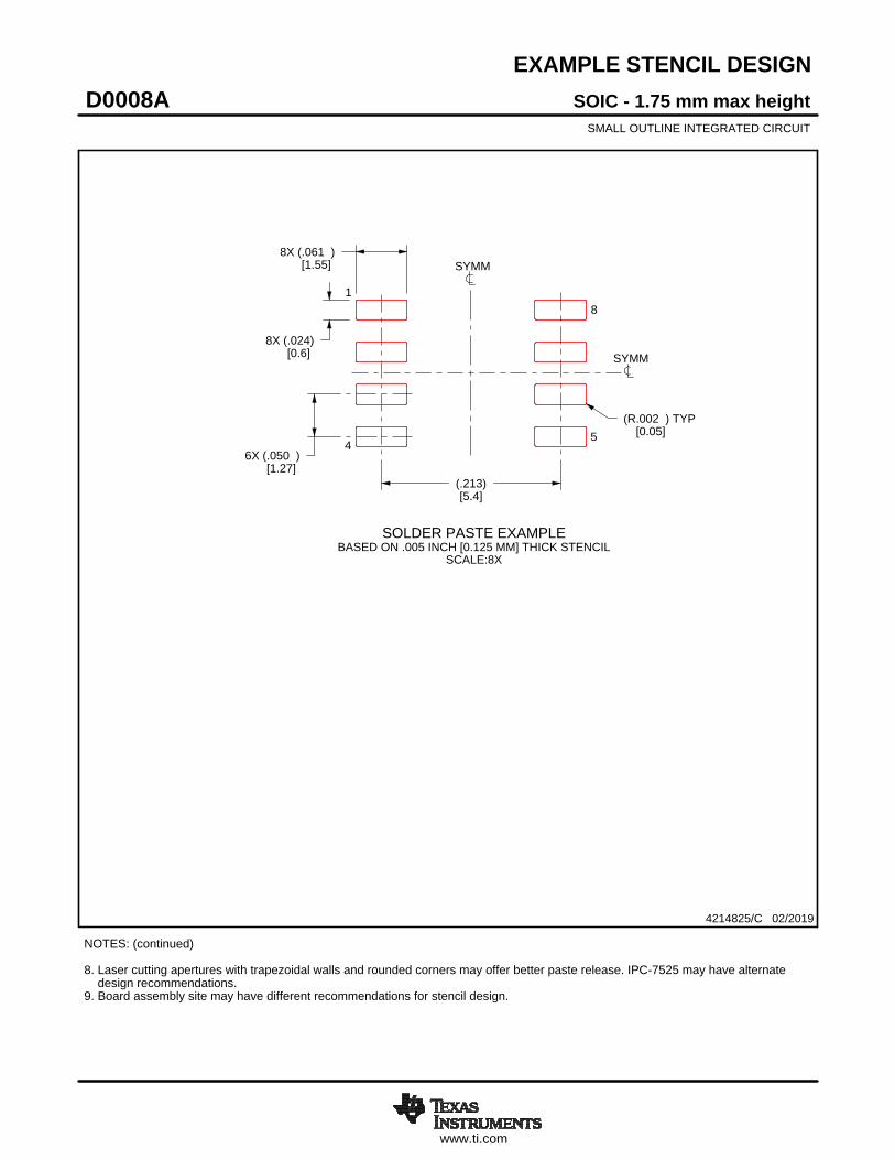
www.ti.com
EXAMPLE STENCIL DESIGN
8X (.061 )[1.55]
8X (.024)[0.6]
6X (.050 )[1.27]
(.213)[5.4]
(R.002 ) TYP[0.05]
SOIC - 1.75 mm max heightD0008ASMALL OUTLINE INTEGRATED CIRCUIT
4214825/C 02/2019
NOTES: (continued) 8. Laser cutting apertures with trapezoidal walls and rounded corners may offer better paste release. IPC-7525 may have alternate design recommendations. 9. Board assembly site may have different recommendations for stencil design.
SOLDER PASTE EXAMPLEBASED ON .005 INCH [0.125 MM] THICK STENCIL
SCALE:8X
SYMM
SYMM
1
45
8


IMPORTANT NOTICE AND DISCLAIMERTI PROVIDES TECHNICAL AND RELIABILITY DATA (INCLUDING DATA SHEETS), DESIGN RESOURCES (INCLUDING REFERENCE DESIGNS), APPLICATION OR OTHER DESIGN ADVICE, WEB TOOLS, SAFETY INFORMATION, AND OTHER RESOURCES “AS IS” AND WITH ALL FAULTS, AND DISCLAIMS ALL WARRANTIES, EXPRESS AND IMPLIED, INCLUDING WITHOUT LIMITATION ANY IMPLIED WARRANTIES OF MERCHANTABILITY, FITNESS FOR A PARTICULAR PURPOSE OR NON-INFRINGEMENT OF THIRD PARTY INTELLECTUAL PROPERTY RIGHTS.These resources are intended for skilled developers designing with TI products. You are solely responsible for (1) selecting the appropriate TI products for your application, (2) designing, validating and testing your application, and (3) ensuring your application meets applicable standards, and any other safety, security, regulatory or other requirements.These resources are subject to change without notice. TI grants you permission to use these resources only for development of an application that uses the TI products described in the resource. Other reproduction and display of these resources is prohibited. No license is granted to any other TI intellectual property right or to any third party intellectual property right. TI disclaims responsibility for, and you will fully indemnify TI and its representatives against, any claims, damages, costs, losses, and liabilities arising out of your use of these resources.TI’s products are provided subject to TI’s Terms of Sale or other applicable terms available either on ti.com or provided in conjunction with such TI products. TI’s provision of these resources does not expand or otherwise alter TI’s applicable warranties or warranty disclaimers for TI products.TI objects to and rejects any additional or different terms you may have proposed. IMPORTANT NOTICE
Mailing Address: Texas Instruments, Post Office Box 655303, Dallas, Texas 75265Copyright © 2022, Texas Instruments Incorporated