Self-similar Cylindrical Ionizing Shock Waves in a Rotational ...
Upload
khangminh22Category
view
0download
0
Air Force Institute of Technology Air Force Institute of Technology
AFIT Scholar AFIT Scholar
Theses and Dissertations Student Graduate Works
3-2003
Total Dose Effects of Ionizing and Non-Ionizing Radiation on Total Dose Effects of Ionizing and Non-Ionizing Radiation on
Piezoresistive Pressure Transducer Chips Piezoresistive Pressure Transducer Chips
Samuel J. Willmon
Follow this and additional works at: https://scholar.afit.edu/etd
Part of the Electronic Devices and Semiconductor Manufacturing Commons, and the Nuclear
Engineering Commons
Recommended Citation Recommended Citation Willmon, Samuel J., "Total Dose Effects of Ionizing and Non-Ionizing Radiation on Piezoresistive Pressure Transducer Chips" (2003). Theses and Dissertations. 4296. https://scholar.afit.edu/etd/4296
This Thesis is brought to you for free and open access by the Student Graduate Works at AFIT Scholar. It has been accepted for inclusion in Theses and Dissertations by an authorized administrator of AFIT Scholar. For more information, please contact [email protected].

./
TOTAL DOSE EFFECTS OF IONIZING AND NON-IONIZING RADIATION
ON PIEZORESISTIVE PRESSURE TRANSDUCER CHIPS
THESIS
Samuel J. Willmon, Captain, USA
AFIT/GNE/ENP/03-11
DEPARTMENT OF THE AIR FORCE
AIR UNIVERSITY
AIR FORCE INSTITUTE OF TECHNOLOGY
wrignt-Katterson Air horce base, unio
APPROVED FOR PUBLIC RELEASE; DISTRIBUTION UNLIMITED

The views expressed in this thesis are those of the author and do not reflect the official policy or position of the United States Air Force, Department of Defense, or the United States Government.

AFIT/GNE/ENP/03-11
TOTAL DOSE EFFECTS OF IONIZING AND NON-IONIZING RADIATION ON PIEZORESISTIVE PRESSURE TRANSDUCER CHIPS
THESIS
Presented to the Faculty
Graduate School of Engineering and Management
Air Force Institute of Technology
Air University
Air Education and Training Command
in Partial Fulfillment of the Requirements for the
Degree of Master of Science (Nuclear Science)
Samuel J. Willmon, BS
Captain, USA
March 2003
APPROVED FOR PUBLIC RELEASE; DISTRIBUTION UNLIMITED

li-
AFIT/GNE/ENP/03-11
TOTAL DOSE EFFECTS OF IONIZING AND NON-IONIZING RADIATION ON PIEZORESISTIVE PRESSURE TRANSDUCER CHIPS
Samuel J. Willmon, BS Captain, USA
Approved:
James C. Petrosky, LTC, (Chairman) date
David Weeks, (MernBer) IV ^/Ur03
date
itis,?^, Paul Kladitis,TeFr, (Member)
/o A^A^O^ date

iv
Acknowledgements
I would like to first thank my wife for her never-ending support throughout this
process. I would also like to express my sincere thanks to my faculty advisor, LTC
James Petrosky for providing guidance when needed, focus when I tended to wander, and
general encouragement throughout this endeavor. I also owe thanks to Mr. Patrick Griffin
of the Sandia Annular Core Research Reactor facility and Mr. Joseph Talnagi of the Ohio
State Research Reactor facility for their personal guidance and insight into reactor
dosimetry and neutron flux characterization.
I am eternally indebted to Mr. Larry Callahan of the Air Force Research
Laboratory for solving my bonding issue and to Mr. Russ Hastings from the Air Force
Institute of Technology for working magic in the machine shop. Lastly, I would like to
thank my fellow classmates for serving as a sounding board and keeping me grounded.
Samuel J. Willmon

v
Table of Contents
Page
Acknowledgements .............................................................................................................iv
List of Figures ................................................................................................................... vii
List of Tables ......................................................................................................................ix
Abstract ................................................................................................................................x
I. Introduction................................................................................................................... 1
Background ................................................................................................................... 1 Problem Statement ........................................................................................................ 2 Scope............................................................................................................................. 2 General Approach......................................................................................................... 3
II. Background ................................................................................................................... 5
Piezoresistive Effect...................................................................................................... 5 Pressure Transducers..................................................................................................... 8 Electrical and Mechanical Properties of Silicon......................................................... 11 Semiconductor Modeling ............................................................................................ 11 Radiation Effects on Semiconductors......................................................................... 15 Defect Effects and Annealing ..................................................................................... 17 Development of Damage Coefficients ........................................................................ 19 Change in Resistivity as a Function of Total Dose ..................................................... 21
III. Experiment .................................................................................................................. 23
Experimental Procedure .............................................................................................. 23 Measurement System Design...................................................................................... 24 Measurement System Characterization....................................................................... 28 Chip Preparation and Characterization....................................................................... 32 Irradiation Tests .......................................................................................................... 34 Annealing .................................................................................................................... 36 Analysis Procedure ..................................................................................................... 37
IV. Results ......................................................................................................................... 40
Initial PISCES-II Model ............................................................................................. 40 Gamma-only Irradiation.............................................................................................. 40 Neutron and Gamma Irradiation................................................................................. 44 Identification of Transducer Vulnerabilities............................................................... 48 Extension of Results to ACRR Shots.......................................................................... 49 Other Observations ..................................................................................................... 50
V. Research Summary ..................................................................................................... 52

vi
Conclusions ................................................................................................................. 52 Ionizing Radiation Damage ........................................................................................ 52 Displacement Damage ................................................................................................ 53 Applications ................................................................................................................ 53 Recommendations for Future Research...................................................................... 54
Appendix A. Extracts from the Irradiation Test Plan.................................................. 55
Test Objectives............................................................................................................ 55 Basic Device Physics Tests......................................................................................... 55 Description of Tests .................................................................................................... 58 Pre-Irradiation Shakedown and Debug Tests ............................................................. 58 Test A1: Gamma-only Irradiation (Gamma Cell) Test ............................................... 59 Test B1: Neutron and Gamma Irradiation (reactor) Test ............................................ 61 Tests A2 & B2: Annealing Tests ................................................................................ 62 Test C1: Dosimetry..................................................................................................... 63 Special Requirements.................................................................................................. 63 Test Equipment ........................................................................................................... 63 OSU Gamma Irradiation Cell Conditions for Tests.................................................... 64 OSURR Conditions for Tests...................................................................................... 64 Annex A-1. piezoresistive Test Control Program Flow Chart................................. 65 Annex A-2. Test Configuration ............................................................................... 66 Annex A-3. Preliminary Dosimetry Calculations .................................................... 67 Gamma Cell Preliminary Calculations. ...................................................................... 67 Beam port #1 Preliminary Calculations. ..................................................................... 68
Appendix B. Measurement System Characterization.................................................. 74
Optoisolator Characterization..................................................................................... 74 Standard Resistor Characterization............................................................................. 78
Appendix C. LANL Tests at the Sandia ACRR.......................................................... 81
Conduct of the Tests ................................................................................................... 81 Neutron Spectrum Characterization............................................................................ 81 Test Pulse Shapes........................................................................................................ 82 Estimated Total Dose Delivered ................................................................................. 83
Appendix D. Sample Output Data ............................................................................... 85
Raw Data..................................................................................................................... 85 Parsed and Conditioned Data ...................................................................................... 86 Representative MathcadTM File ................................................................................... 86
Bibliography...................................................................................................................... 88
Vita.................................................................................................................................... 90

vii
List of Figures
Figure Page
1. “Many-valley” model equipotential surfaces................................................................ 7
2. General-purpose wheatstone bridge.............................................................................. 9
3. Ametek Piezoresistive Chip ........................................................................................ 10
4. Contour Plot of Stress lines......................................................................................... 10
5. P-channel model.......................................................................................................... 12
6. Effects of Defect Centers within the Bandgap............................................................ 18
7. Mechanism Importance as a Function of Neutron Fluence ........................................ 20
8. Irradiation scheme....................................................................................................... 24
9. Measurement system design ....................................................................................... 25
10. Measurement System Control Box (side view) .......................................................... 26
11. Measurement System Control Box (rear view) .......................................................... 26
12. Annealing Station (top view) ...................................................................................... 27
13. Optoisolator on-state ................................................................................................... 29
14. Optoisolator off-state .................................................................................................. 30
15. Standard resistor bench test (without switches) .......................................................... 31
16. Standard resistor bench test (with switches)............................................................... 32
17. Piezoresistive chip ....................................................................................................... 33
18. Piezoresistive chip on transistor mount ...................................................................... 33
19. Baseline piezoresistive chip characterization ............................................................. 34
20. P1 response during first irradiation cycle ................................................................... 41

viii
21. Change in measured current ........................................................................................ 42
22. Gamma Cell Irradiation Results.................................................................................. 43
23. Beam port measurements............................................................................................ 45
24. Reactor irradiation results ........................................................................................... 46
25. Change in resistance as a function of neutron dose .................................................... 47
26. Temperature profile of beam port #1 .......................................................................... 48
27. Piezoresistive transducer construct (side view) .......................................................... 56
28. Piezoresistive Transducer Circuit Board..................................................................... 56
29. Enlarged Ametek piezoresistive Chip (top view) ....................................................... 57
30. piezoresistive Test Program Control Flow Chart........................................................ 65
31. Test Configuration ...................................................................................................... 66
32. OSURR beam port #1 neutron spectrum .................................................................... 69
33. Optoisolator forward voltage [V]................................................................................ 75
34. Switch limiting current ................................................................................................ 76
35. Switch leakage current (semi- log plot) ....................................................................... 77
36. 10kΩ resistor characterization (without switches)...................................................... 79
37. 10KΩ resistor characterization (with switches) .......................................................... 80
38. Relative neutron yield per MeV vs neutron energy .................................................... 82
39. Representative Sandia ACRR pulses (7540-7542) ..................................................... 83
40. Representative raw data from output file .................................................................... 85
41. Representative parsed and conditioned data ............................................................... 86
42. Representative MathcadTM data manipulation file ...................................................... 87

ix
List of Tables
Table Page
1. Fundamental Properties of Silicon.............................................................................. 11
2. Gamma Cell Total Dose Distribution ......................................................................... 41
3. Neutron total dose distribution.................................................................................... 44
4. Activation data ............................................................................................................ 69
5. Optoisolator operating parameters.............................................................................. 74

x
AFIT/GNE/ENP/03-11
Abstract
The effects of ionizing and non- ionizing radiation on the resistivity of silicon-
based, piezoresistive bulk micro-machined chips from pressure transducers were
examined. Standard current-voltage (I-V) measurements were taken in-situ and post-
irradiation during isothermal annealing at room temperature. One group of chips was
irradiated to a maximum total gamma dose of 1MradSi in the 11,000 Ci 60Co gamma cell
at Ohio State University. The second group of chips was irradiated at the Ohio State
University Research Reactor facility to a maximum total neutron dose of 4 MradSi using
beam port #1.
The resistivity was shown to decrease during gamma irradiation as a result of
Compton current generation and increase during neutron irradiation as a result of
displacement damage. During irradiation in the gamma cell, the chips exhibited a 0.45 ±
0.19 % decrease in resistivity at saturation. During the neutron and gamma irradiation in
the reactor, the chips exhibited a peak change in resistivity of 2.503 ± 0.003% at 2
MradSi, 3.055 ±0.002% at 3 MradSi, and 3.6921% (with unknown uncertainty) at 4
MradSi. Regardless of the total dose received, all chips demonstrated a permanent change
in resistivity of 0.7697 ± 0.0006% at room temperature.

1
I. Introduction
Background
This research examines the relationship between the total radiation dose from
ionizing and non-ionizing radiation and the resistivity of a piezoresistive chip in an effort
to determine the contributions of ionizing and non- ionizing irradiation to piezoresistive
transducer failure. For application purposes, this research specifically examines the
behavior of silicon chips as fabricated for use in the Ametek IPTG-0600DSFS model
transducer.
This research stems from problems encountered at the Los Alamos National
Laboratory (LANL), New Mexico, related to the stockpile stewardship program. In
essence, an experiment at LANL requires that the internal pressure of a containment
vessel be taken while the components are irradiated using the annular core research
reactor (ACRR) at Sandia, New Mexico. This provides the researchers at LANL a great
degree of confidence that no possible contaminants have leaked from the vessel. In
addition, further tests will require pressure and acceleration measurements as a shock
wave is propagated through a similar vessel. To this end, the researchers at LANL have
incorporated a piezoresistive pressure transducer into their test design.
Thus far, the researchers at LANL, in collaboration with Arizona State University,
have made several observations concerning their piezoresistive pressure transducers.
They have observed that several models fail initialization tests after sitting in a storage
vault where an estimated gamma flux exists of 105 cm-2 s-1; some models fail single
reactor pulses (20-30 MWth, with an estimated pulse width of 10ms); and some models
survive multiple reactor pulses. Further investigations at Arizona State University have

2
tested the functionality of piezoresistive pressure transducers while irradiated in a gamma
cell and similar results were discovered.1
Several factors exist which complicate the interpretation of the studies performed
thus far. To date, no solid dosimetry tests have been performed to determine the actual
dose delivered to the piezoresistive pressure transducers in either the storage vault or the
ACRR at Sandia. In each test, the transducers were incorporated “as fabricated” and no
investigations into the design and inner structure of the transducers have been performed.
With sponsorship from the Defense Threat Reduction Agency, Washington D.C.,
this research serves as an initial investigation into the behavior and performance of
piezoresistive pressure transducers in radiation environments.
Problem Statement
The goals of this thesis are: (1) to characterize the relationship between total dose
and resistivity across the piezoresistive chip’s Wheatstone bridge, (2) identify the chip’s
radiation dose limits, (3) characterize the recovery profile as a function of operating
voltage and temperature, and (4) to investigate possible annealing conditions which allow
the devices to recover post-irradiation.
Scope
This research investigates the change in resistivity across a piezoresistive silicon
chip fabricated for use in a pressure transducer while irradiated. Two sources of radiation
are used in this research: a 60Co gamma cell (providing ionizing radiation only) at the
Ohio State University (OSU) reactor facility, and a research reactor (providing ionizing

3
and non- ionizing radiation, also at OSU). In-situ I-V measurements are taken during
irradiation and during an annealing period (at room temperature).
General Approach
The approach to this research follows a “simple” theory-model-experiment cycle.
After developing the theory outlining the effects of radiation on silicon, a model is
presented which serves to predict the expected behavior following irradiation, then the
experiment confirms or denies the hypothesis presented by the model. Based on the
outcome of the experiment, the theory may require refinement in order to justify altering
the proposed model.
Following a comprehensive, open-source literature search, several initial findings
were evident. No current work exists examining the effect of radiation on piezoresistive
materials. Numerical modeling and analysis is outside the scope of and time available
for this research. Many studies have been performed on the radiation effects on silicon
crystals and electronic components. An initial investigation into the design and structure
of the Ametek transducer identified several points of failure. Based on these findings, the
focus of this research is narrowed to the effect of radiation on the piezoresistive chip.
That no current studies have explored the influence of radiation on the behavior of
piezoresistive materials stems most likely from the nature of radiation environments. The
Institute of Electrical and Electronics Engineers (IEEE) categorizes radiation
environments as the following: the space environment, the nuclear reactor environment,
and the nuclear weapon (following detonation) environment. None of these
environments explicitly calls for the use of a piezoresistive pressure sensor. In the case
4
of a nuclear reactor, for example, it is more sound to not employ a transducer in the
radiation environment than to attempt to monitor the coolant pressure via a transducer
near the reactor’s core.
Previous work in the area of radiation effects on electronic devices is relied upon
in order to extrapolate the effect of the radiation on the entire transducer. In addition, the
radiation sources used in this research at OSU fit a long duration, square pulse and the
reactor pulses used by the LANL researchers at the ACRR in Sandia fit a narrow, short
pulse. Due to the differing pulse shapes, the results of this research are further
extrapolated to predict the behavior of the piezoresistive chip following a pulse of
radiation from the ACRR in Sandia.

5
II. Background
This chapter develops the theory regarding the piezoresistive effect and
demonstrates the construct of piezoresistive pressure transducers. In addition, the model
used in this research and the effects of radiation on semiconductors is presented.
Piezoresistive Effect
The first published documents outlining the nature of the piezoresistance effect
appear in the 1930’s. The work of the Curie brothers in 1880 (who are credited with
discovering the piezoelectric effect) and Woldemar Voigt, who in 1928 published
Lehrbuch der Kristallphsyik, made great strides in relating the properties of crystals to
their geometric symmetry. Professor Bridgman at Harvard University was the first to
study the effects of a mechanical stress on the electrical resistance of crystals.2 Assuming
Ohm’s law holds, Bridgman first expresses the electric field vector , E, as a function of
the current vector:
(1)
where E is the potential gradient vector, q is the current vector, and r is the matrix of
coefficients which satisfy the equation. Bridgman asserts that if a mechanical stress is
applied to the crystal, the matrix of coefficients will change according to the following
form:
(2)
E→
r J→
δri j,
δr1 1,
δr1 2,
δr1 3,
δr1 2,
δr2 2,
δr3 2,
δr1 3,
δr3 2,
δr3 3,

6
Research examining the piezoelectric effect prior to the 1950’s focused primarily
on identifying materials with piezoelectric properties. Once silicon had been identified as
having piezoelectric properties, researchers focused on identifying silicon’s piezoresistive
coefficients. These measurements allowed for the identification of the relationship
between the induced electric field caused by an applied stress or strain (and conversely,
the displacement caused by an applied electric field).3 It was not until nearly a quarter of
a century later that Charles Smith of the Bell Laboratories in New Jersey described the
piezoresistive effect in silicon and provided the complete tensor that characterizes the
piezoresistive coefficients.4 Smith continued Bridgman’s formulation by expressing the
change in the electric field in terms of equation (2):
(3)
where Smith has re-defined the matrix of coefficients as d?. For convenience, Smith
divides both sides by the scalar resistivity (?) resulting in:
(4)
where ? is defined as ? = (d? i,j)/?. Smith further defines ? in terms of the applied stress
X as:
(5)
where ? is the matrix of piezoresistance coefficients and X is the matrix that describes
the applied stress. Given a constant current, equation (4) can be written in terms of the
piezoresistance coefficients and the applied stress:
δE→
δρ J→⋅
δE→
ρ∆ J→
∆ ΠΧ

7
(6)
While Bridgman took a mathematical approach to describing the piezoresistance
effect, Smith made the additional step (in conjunction with C. Herring, also of Bell
Laboratories) in attempting to develop the theory explaining why the piezoresistance
effect occurs. To accomplish this, Smith employed the “many valley” lattice model.
According to this model, electron equipotential regions appear as ellipsoids along the
coordinate axes. In an unstressed crystal, these regions are symmetrical and of equal size
as the electrons have no preferred location. As shown in Figure 1, a stress that is applied
to the crystal (here in the [1,0,0] direction), gives rise to a change in the equipotential
regions and electrons are “transferred” in a preferred direction.
Figure 1: “Many-valley” model equipotential surfaces
δE→
ρ∆Χ J
→
µyy
µyx
µxy
µxx

8
Smith asserts that this equipotential surface change results in a change in the
lattice mobility. In Figure 1, the direction and magnitude of the arrows associated with
the mobility indicate the change in mobility, µ. The dashed lines indicate the changes in
the equipotential surfaces.
In applying his theory, Smith discovered that in some cases his predicted values
for the piezoresistance coefficients did not agree with work previously done by
Bridgman. With assistance from Herring, Smith indicates that other electron transfer
mechanisms must exist. Smith postulated that a strain on a crystal produces “change in
resistance through its action on the phonons, on the electrons, and on the coupling
between them.”4
Further refinement of Smith’s theory on the piezoresistance effect has not been
accomplished. Although one can apply the Hamiltonian and other many-bodied physics
concepts to a crystalline lattice, solving these systems of equations in terms of electron
and phonon interactions requires complete knowledge (in time, position, and energy) of
the nuclei, electrons, and phonons.5 Even with the supercomputing capability available
today, this task is daunting. As a result, Smith’s theory is generally accepted. While
Smith’s theory does not provide a means to calculate piezoresistance coefficients
explicitly, piezoresistance measurements can be made and the theory applied accordingly.
Pressure Transducers
The fundamental goal of any transducer is to transform a given physical
parameter (force, mass, velocity, etc.) into an electric signal. Duane Tandeske offers
several parameters that can be used to determine the type of transducer appropriate for a
given situation. The most common parameters being “range, accuracy, size and price.”6

9
Piezoresistive pressure transducers capitalize on all four of the selection parameters
given.
In the typical piezoresistive transducer, four resistors are arranged in a
Wheatstone bridge. In order to account for the resistance changes due to temperature,
temperature-compensating resistors are often included in the circuit. Figure 2 shows a
general-purpose Wheatstone bridge.
Figure 2: General-purpose wheatstone bridge
The Wheatstone bridge as shown in Figure 2 is fabricated on a thin chip of silicon
where the expected pressure is applied to the center of the bulk micro-machined silicon
chip. A common technique is to create the resistive circuit path (a p-channel) by ion
implanting boron into an n-type silicon substrate. In order to minimize leakage, the
substrate is reverse-biased, which creates a depletion region at the pn-junction.

10
The four resistors of the Wheatstone bridge are fabricated as strain gages and the
resulting circuit is shown in Figure 3. A pressure applied to the center of the chip creates
stress lines within the crystal. The location of the piezoresistive strain gages capitalizes
on the locations of the maximum induced strain. A schematic depicting the stress lines
created is shown in Figure 4. When taken together, the simple logic behind the
piezoresistive pressure transducer is apparent.
Figure 3: Ametek Piezoresistive Chip
Figure 4: Contour Plot of Stress lines6
Wheatstone bridge resistors
Maximum stress at the edges
—Ji
L'1

11
Electrical and Mechanical Properties of Silicon
Because of its semi-conducting properties, the relatively high level of the
development in the manufacturing processes involved in generating ultra-pure silicon,
and its high piezoelectric coefficients, silicon-based piezoelectric devices remain at the
core of current technological development. Silicon’s tensile and compressive strengths
are greater than steel and it has an ability to sustain a greater number of cycles of tension
and compression than steel. These physical properties combined with its semi-
conducting properties make single-crystal silicon an excellent material for a transducer.7
Table 1 lists several fundamental properties of silicon.
A wide range of silicon based micro-electromechanical systems (MEMS)
employed in terrestrial applications currently exists. The low weight, cost, and power
requirements of MEMS devices combined with the ability to achieve cost effective
redundancy make them ideal for space applications as well.8 The continued development
of space technology and the need to collect data in radiation environments on earth
requires the design of sensors capable of surviving expected radiation dose levels.
Table 1: Fundamental Properties of Silicon9
Property Value Band gap (300K) 1.12 eV
Electron Mobility (300K) 1500 (cm2 V-1 s-1) Hole Mobility (300K) 450 (cm2 V-1 s-1) Ionization Density10 4.3x10¹³ (cm-3 rad-1) Intrinsic Resistivity 2.3x10⁵ (O-cm)
Carrier lifetime 10-6 (s)
Semiconductor Modeling
Several modeling tools exist in order to examine the behavior of semiconductors.
This research incorporated PISCES-II (version 9009-Win32 x86) modeling in order to

12
obtain benchmarks for the current measurements obtained. In essence, the PISCES-II
code solves charge carrier transport equations and Poisson’s equation in two
dimensions.11 Given a physical description of the semiconductor (material, length and
width, as well as dopant type and concentration), the location of electrodes, and the
applied potential, PISCES-II calculates the current at the electrodes.
The two electrical paths from VHIGH to VLOW in Figure 2 can be represented as
two rods of p-type silicon with electrodes placed on the faces of both ends (shown in
Figure 5). Using the outer dimensions of the chip as a reference, the channel width (W)
and length (L) were measured from the enlarged photograph of the chip in Figure 3
(4.7 ±0.01 µm and 5.618 ± 0.001 mm, respectively). The depth (D) of the channel of 10
± 1 µm was estimated from current literature on piezoresistive fabrication techniques.
Figure 5: P-channel model
The resistivity of the p-type silicon is given by the following equation12:
(7)
where the area (A) has been multiplied by two in order to account for both conducting
channels. Initial resistance measurements of the p-channels resulted in an average
ρR 2A( )
L
Electrode Electrode

13
resistance (R) of 9.7 ± 0.1 kO. Equation (7) results in a calculated resistivity of 0.016 ±
0.002 O-cm.
There are many references on semiconductor materials that show the relationship
between the dopant concentration and the resistivity in silicon. Using one such figure in
Van Lint’s book Mechanisms of Radiation Effects in Electronic Materials (Vol. 1)10, the
dopant concentration of the Ametek p-channel is approximately 1019 cm-3. The physical
parameters, the estimated dopant concentration, the placement of the electrodes, and the
carrier lifetimes given in Table 1 provide all of the necessary information required by
PISCES-II to solve the continuity equations and Poisson’s equation.
The continuity equations describe the transport of charge carriers in
semiconductors as function of position and time.13 In one dimension, the continuity
equations are:
(8)
(9)
where Jp,n are the hole and electron currents, p and n are the carrier densities, q is the
fundamental unit of charge, and U and G are the recombination and generation rate
densities, respectively. The following equations express the hole and electron currents in
terms of the electric field and their respective diffusion coefficients13:
(10)
tpd
d
1−
q xJp
dd
Up x t,( )− G x t,( )+
tnd
d
1−q x
Jndd
Un x t,( )− G x t,( )+
Jp qµppE qDp xpd
d
−

14
(11)
where µp,n are the carrier mobilities, Dp,n are the carrier diffusion coefficients, and E is the
electric field. The diffusion coefficients are related to the diffusion length and carrier
lifetime via the following equation10:
(12)
The diffusion coefficients are also related to the carrier mobility and the temperature
through Einstein’s relation10 (written here for electrons):
(13)
where k is Boltzman’s constant, and T is the temperature [K].
“Poisson’s relates the electric field distribution to mobile charge and active
impurity densities:”13
(14)
where e is the permittivity of the material, and N is the dopant concentration.
The modeling effort was limited due to the inability of PISCES-II to include the
effects of ionizing and non-ionizing radiation directly. Despite this limitation, the results
from the PISCES-II model were expected to favorably compare to baseline tests
performed on the chips prior to irradiation. The modeling results then indicate the lower
limit on the in-situ measurements during irradiation.
Dn µnkT
q
xEd
d
q
εp n− N+( )
Ln Dnτn
Jn qµnnE qDn xnd
d
−

15
Radiation Effects on Semiconductors
Despite an exponential growth in the application of silicon technology,
researchers have devoted little effort toward investigating the effects of radiation on
piezoresistive devices. Volumes, however, have been written describing theories
regarding the radiation damage mechanisms in bulk silicon. These studies have
characterized the changes in carrier concentration, mobility, and lifetime as a function of
total dose in silicon. 14
Matthias Werner and Wolfgang Fahrner (ranking members of IEEE) call for
increased studies of MEMS devices in “harsh” environments. However, their paper
focuses on the influences of temperature on device performance and discounts the
application of Si-Si devices due to silicon’s small band gap.15 Knudson (et al)
investigated the effects of radiation on MEMS accelerometers through proton and heavy
ion bombardment. Their conclusions, however, fall short of identifying the relationship
between the postulated damage mechanisms and the resistivity of the sensor material.16
Swarupa Padgaonkar (et al) employed a 14 MeV neutron generator in his 1990
research into the effects of high energy neutrons on the Hall mobility, carrier
concentration, energy levels of defect sites, and the minority carrier lifetime in
phosphorus doped silicon. Padgaonkar found that the energy levels of the defect sites
were identical in both cases. Padgaonkar also found that high-energy neutron irradiation
resulted in a degradation in mobility.17
C. I. Lee (et al) conducted research into the effects of radiation on MEMS
accelerometers and was able to identify a difference between entire sensor irradiation and

16
sensing element only irradiation. Their research, however, failed to characterize the
decline in sensor function as a result of the dose received or its recovery profile.18
The principle source of ionizing radiation damage stems from Compton
scattering. 19 Incident gamma rays that elastically scatter off of atomic electrons produce
Compton electrons. While electrons with sufficient energy to displace silicon atoms
within the lattice can create vacancy- interstitial pairs, the probability for scattering is
much greater than the probability of generating vacancy-interstitial pairs. The electrons
generated can also scatter and produce additional ionized electrons, recombine with
holes, occupy trap sites, or exit the device as unwanted current (photocurrent). In the
literature, the creation of ionized electrons (which leave behind holes) is often referred to
as carrier injection. In terms of the quantity of electron-hole pairs created, Low Level
Injection (LLI) occurs when fewer carriers are injected per unit volume than original
carrier concentration. Alternatively, High Level Injection (HLI) occurs when more
carriers are injected per unit volume than the original carrier concentration. 20
Messenger states that due to silicon’s low displacement cross section (3x10-24
cm2) and the range of neutrons in silicon (on the order to centimeters), incident neutrons
will produce uniformly distributed collision sites throughout the crystal and most likely
leave the crystal following a single collision. When a neutron with sufficient energy
collides with an atom, it will displace the atom from the crystal lattice. The displacement
threshold energy is 20 eV for silicon. The displaced atom (also referred to as a primary
knock on atom, PKA) will lose its energy through ionizing and non- ionizing interactions
and come to rest in an energetically favorable location with the lattice. The PKA leaves
behind a track of vacancy- interstitial pairs until it no longer has enough energy to

17
displace any more atoms. This final location, however, need not be in a location that
follows the pattern of the crystal structure. The interstitials leave behind a lattice
vacancy. Because the majority of the vacancy- interstitial pairs lie within a few atomic
spacings of each other, they recombine with a high probability. Messenger states that this
accounts for nearly an annealing of 95% of the vacancy- interstitial pairs produced in this
fashion. While interstitials do not form electrically active defect sites, vacancies serve as
trapping and recombination centers and reduce the carrier mobility, density, and minority
carrier lifetime.14 Additionally, research has shown that vacancies are mobile in p-type
silicon at temperatures above 160K.21
Defect Effects and Annealing
“The words anneal and annealing refer to the partial or total self-healing of an
electronic component or system after exposure to damaging nuclear radiation.”20 The
annealing process in a crystal is highly temperature and time dependent. As temperature
increases, the thermal energy imparted to defects within the lattice gives them sufficient
energy to become mobile. In this manner, vacancies and interstitials may recombine. It
is also possible, however, for defect atoms within the lattice structure to form stable
associations with existing impurities and further degrade device performance.20 The
longer the device is allowed to anneal at a temperature at which defects are mobile, the
more defects that will anneal. Generally, the annealing process takes the form of a
decaying exponential.
Following the generation of defect centers within the bandgap, several possible
effects may occur. The primary effects of defect centers are electron-hole pair

18
generation, recombination, trapping, compensation, and tunneling (the first four of which
are depicted in Figure 6: Effects of Defect Centers within the Bandgap).22
Figure 6: Effects of Defect Centers within the Bandgap
A valence band electron may gain sufficient thermal energy to become excited to
the defect center. Further thermal excitation may allow the electron to jump to the
conduction band. Defect centers located near the mid-gap region contribute the most to
electron-hole pair generation.
Recombination occurs when a defect center captures a charge carrier and then
captures another of the opposite sign. The average amount of time a charge carrier spends
within the bandgap is referred to as the recombination lifetime.
Charge carriers may also become temporarily trapped in a shallow level defect.
Once trapped, the charge carrier is later released back to its energy band.

19
Defects may also compensate for donors or acceptors, depending on their charge
state and location within the bandgap. In this manner, deep lying acceptor-type defects
compensate for donor free electrons. This results in the decrease in the carrier
concentration.
Development of Damage Coefficients
As described above, the primary radiation effects observed in semiconductors are
a change in carrier mobility, carrier density, carrier lifetime, and the generation of a
photocurrent. In order to predict how these parameters will change following irradiation,
damage coefficients have been developed which describe the impact of the radiation on
each parameter.10 The minority carrier lifetime following irradiation is given by:
(15)
where t is the minority carrier lifetime following irradiation, to is the minority carrier
lifetime prior to irradiation, Kt is the lifetime damage coefficient, and F is the radiation
fluence. Similarly, the mobility following irradiation is given by:
(16)
where µ is the mobility following irradiation, µLo is the lattice mobility prior to
irradiation, µIo is the impurity scattering mobility prior to irradiation, Kµ is the mobility
damage coefficient. And the electron concentration following irradiation is given by:
(17)
1
τ
1
τ oK τ Φ⋅+
1
µ
1
µLo
1
µIo+ Kµ Φ⋅+
n no Kn Φ⋅−

20
where n is the electron density following irradiation, no is the electron density prior to
irradiation, Kn is the carrier concentration damage coefficient. Kn can also be thought of
as the carrier removal rate. All of the damage coefficients presented in equations (15)
through (17) are functions of the “Fermi level, temperature, and irradiation
composition.”10
As shown in Figure 7, the radiation damage mechanisms described above become
important only once the neutron fluence rises above distinct threshold values. While the
graph specifically described the impact of neutron fluence on the damage mechanisms for
n-type silicon with a resistivity of 2 ohm-cm, the information contained in the figure
applies to the p-type silicon used in this research as well.
Figure 7: Mechanism Importance as a Function of Neutron Fluence22
1.0
E c o.« * ^3
0.0
1 T n N^TYPE SILICON (I ohOk-cMll FlS5J0f< NCUTnoNS
—T T" — r -
^ V fl/ft, \ \
\ \ \-
(T^-10^«J \
\
\
1 1 \^ -^ V
10- 10^ JO ,11 .11 10'" 10 10 10 13 10 14 to 11

21
Change in Resistivity as a Function of Total Dose
With electrical resistivity is defined as the inverse of conductivity, the change in
resistivity is given by the following equation:
(18)
where eo is the fundamental unit of charge, dn is the excess electron density, dp is the
excess hole density, and the µ-terms are their respective mobilities.
In the case of ionizing radiation, the primary effect is observed as an excess of
minority charge carriers. In p-type silicon, where the electrons are the minority charge
carrier, the addition of holes through ionization is negligible compared to the initial
density of holes, therefore, equation (18) reduces to:
(19)
By re-arranging equation (17) and substituting the change in the number of charge
carriers as a function of radiation fluence, a negative change in resistance is predicted:
(20)
As shown in Figure 7, however, neutron irradiation at high fluence levels affects
all three of the carrier parameters. Enough information is not gained from current
measurements to explicitly solve the Poisson and carrier current equations given in the
preceding section. Information concerning the behavior of the resulting change in
resistivity can be deduced from the damage coefficient relations.
δρ1
eo δnµn δpµp+( )
δρ1
eo δnµn( )
δρ1−
eo Kn Φµn⋅( )

22
Based on the form of equation (15), carrier lifetimes will decrease as the fluence
increases. Similarly, from equation (16) it is evident that the mobility will increase as the
fluence increases. And as seen in the case of ionizing radiation, the number of excess
charge carriers decreases proportionally with the increase in fluence.

23
III. Experiment
The experimental procedure used in this research consists of the measurement
system design and characterization, chip preparation and characterization, gamma cell
irradiation, reactor irradiation, and finally data analysis. This research utilized the
piezoresistive chips from the Ametek IPTG-600 integrated pressure transducer.
Experimental Procedure
From the problem statement, the primary goal of this research is to determine the
effect of ionizing and non- ionizing radiation in piezoresistive silicon chips. Because the
reactor environment consists of both gammas and neutrons, the contribution of the
photocurrent generated must be accounted for in the in-situ measurements. In order to
determine the magnitude of the photocurrent generated during irradiation in the reactor,
the gamma cell at Ohio State University (OSU) was used.
Time at both the gamma cell facility and the reactor at OSU and budget served as
the primary constraints during the development of the experimental procedure. In order
to achieve the goal of obtaining statistically significant results, four devices were
obtained from Ametek for the gamma cell irradiation and additional four devices for the
reactor irradiation tests. In order to maximize the time available, a step-wise total dose
irradiation scheme was developed. As shown in Figure 8, the irradiation scheme starts
with all four devices being irradiated simultaneously. This allows for a sample size
during the first irradiation cycle of four. As each 25% interval of the total dose is
reached, one device is removed. Clearly, any results from the final irradiation cycle with
a sample size of one are suspect.

24
Sample Size: 4 3 2 1
D1
D2
D3
D4
Figure 8: Irradiation scheme
Measurement System Design
A Keithley-237 Signal Measurement Unit, SMU, served as the primary
measurement unit and focal point of the measurement system. The SMU allows the user
to set operating parameters and collect data using via a GPIB card. As the SMU does not
have the ability to provide a voltage or current source to multiple independent devices, a
control box is needed. In order to provide in-situ measurements during irradiation and
during annealing, test mounts are needed for the gamma cell, the beam port, and an
annealing station. Figure 9 shows a schematic of the measurement system design.

25
Figure 9: Measurement system design
In order to reduce the leakage current contribution to the measurements, eight
4N37 optoisolators were used to serve as switches in the control box (see Figure 10 and
9). The optoisolators consist of an LED connected to a transistor via a light pipe. The
LED and the transistor are isolated from external light sources by the packaging material.
By connecting the transistor side of the optoisolators in parallel to the output-high
terminal on the SMU, current could pass through only one piezoresistive chip at a time.
The eight output pins of the parallel port on the CPU were individually wired to the
optoisolator LED inputs. Sending the correct binary bit to the parallel port turned on a
specific optoisolator. Standard LEDs mounted onto the control box allowed the user to
follow system operations. Twelve coaxial cable connectors were connected to the eight
optoisolator emitter terminals in order to provide connectivity with radiation stations one
through four, and annealing stations one through eight. Radiation stations one through
four were controlled by the same optoisolators as the annealing stations one through four.

26
Figure 10: Measurement System Control Box (side view)
Figure 11: Measurement System Control Box (rear view)

27
Two irradiation stations were designed – one for the gamma cell irradiation, one
for the reactor irradiation. An additional station was designed to perform measurements
during annealing. The gamma irradiation station was constructed from a 1mm thick
aluminum hobby box in order to ensure that charged particle equilibrium was maintained
during irradiation in the gamma cell. A 124-pin socket soldered to a breadboard mounted
inside of the hobby box allowed the dip-mounted chips to be slipped into designated
sockets. Similarly, the beam port irradiation station was constructed from four inch long,
5-inch diameter PVC tube with the chip sockets mounted a Plexiglass plate attached to
one end. A thin Plexiglas plate mounted in the center of the tube was fitted with coaxial
cable connectors. A final Plexiglass plate mounted on the rear of the station was fitted
with a threaded Plexiglass rod that allowed the entire station to be screwed onto the end
of a paraffin plug. This arrangement provided additional radiation shielding by
preventing radiation from streaming out of the beam port. Similar to the gamma cell
station, the annealing station (see Figure 12) was constructed from an aluminum hobby
box with eight coaxial connectors to provide connectivity with the main control box.
Figure 12: Annealing Station (top view)

28
A type-K thermocouple was used during the beam port irradiation runs in order to
monitor the temperature inside the beam port at the chips’ location. The junction
between thermocouple cable and coaxial cable was immersed in liquid nitrogen to move
the reference junction temperature away from room temperature. An exponential fit to
the type-K thermocouple data chart allowed the test control program to convert the
measured voltage directly into a temperature reading. Thermocouple accuracy in the
temperature range near 300K (room temperature) is ± 2.2 oC. When used, the
thermocouple was connected to the control box at annealing station eight.
A Visual Basic program, written as a user interface, controlled all operations
performed by the measurement system. The program performed connectivity checks,
system warm up procedures, controlled measurement cycle sequencing, established
operating parameters for the SMU, controlled the optoisolators, logged data, and
maintained operational system log.
Measurement System Characterization
Once completed with the measurement system design, a series of tests were
performed in order to determine the effectiveness of the measurement system. Principle
operating parameters of the measurement system are the optoisolator leakage currents
and the maximum passable currents. In order to identify these two parameters, the
optoisolators were tested in their on and off states.
In order to test the on-state condition, the transistor output current was measured
as a function of applied voltage to the transistor input. The on-state current
measurements (as shown in Figure 13), indicate a degree of variability in the maximum
passable current between the optoisolators. While the optoisolators may serve as variable

29
resistors, with an expected p-channel current of 10µA (from V=IR) with an applied
voltage of one volt, it is clear that none of the optoisolators limit the expected current.
Statistical analysis of the results from the on-state measurements shows that the average
relative error in the measurements of the optoisolators is less than 0.3%.
Figure 13: Optoisolator on-state
In order to test the off-state condition, the transistor output current was again
measured as a function of applied voltage to the transistor input. This time, the
optoisolators were disconnected from the CPU in order to disrupt the power to the LEDs.
As shown in Figure 14, the results from the off-state condition tests indicate that the
maximum contribution to system measurements owing to leakage from the optoisolators
is on the order of 10nA. Statistical analysis of the results of the off-state measurements
0
0.005
0.01
0.015
0.02
0.025
0 1 2 3 4 5 6 7 8
Applied Voltage [V]
Mea
sure
d C
urre
nt [
A]
S1 S2 S3 S4 S5 S6 S7 S8

30
shows that the relative standard deviation does not fall below 10% unless the measured
signal is above 25nA.
Figure 14: Optoisolator off-state
Following the on- and off-state condition tests, a standard 10kO (±10%) resistor
was used to bench-test the measurement system. In order to test the system without
including the optoisolators, the resistor was hard wired to the control box at the SMU
terminals using jump cables. As shown in Figure 15, system noise does not impact the
current measurements at voltages above 2mA (labeled as “error threshold”).
1.0E-12
1.0E-11
1.0E-10
1.0E-09
1.0E-08
0 1 2 3 4 5 6 7 8 9
Applied Voltage [V]
Mea
sure
d C
urre
nt [A
]
S1 S2 S3 S4 S5 S6 S7 S8

31
Figure 15: Standard resistor bench test (without switches)
The second bench test of the measurement system included the optoisolators. For
this test, the 10kO resistor was hard wired to the optoisolator output terminal, one at a
time, and jumped to the SMU input terminal. The results of this test show that the
calculated resistance, which should fall within 10% of 10kO, does not meet the specified
tolerance until the applied voltage is greater than 0.1V.
5 OOE-HOI
4 OOE-HOI
3 OOE-'Ol
2 OOE-'Ol
1 OOE-HOI
^ OOOE-HOO
-1 OOE-'Ol
-2 OOE-'Ol
-3 OOE-'Ol
O^QOl
•
♦ Error Threshold
•*•*•«
OilOl 0 01 0 1
Applied Votldgv \V
10

32
Figure 16: Standard resistor bench test (with switches)
Chip Preparation and Characterization
Chip preparation consisted of removing the transducer housing, extracting the
chip, slicing the manufactured chip mount, remounting the chip on standard dips, and
wire bonding gold wires from the dip posts to the chip contact pads. The removal and
extraction of the chips occurred in the laboratory at Air Force Institute of Technology
(AFIT). The slicing, remounting, and wire bonding took place at the Air Force Research
Laboratory (AFRL), also at the Wright-Patterson Air Force base.
A standard Dremel® tool was used to breach the transducer housing. Once the
transducer housing was sufficiently reduced, the piezoresistive chips were removed,
5
10
15
20
0.0001 0.001 0.01 0.1 1 10
Applied Voltage [V]
Cal
cula
ted
Res
ista
nce
[kO
hm]
S1 S2 S3 S4 S5 S6 S7 S8

33
cleaned in alcohol, and taken to AFRL (see Figure 17). At AFRL, a diamond blade axial
saw was used to slice the chip mounts to within approximately 1mm from the chip.
Following the slicing stage, the chips were again cleaned in alcohol and remounted to
standard dips with epoxy. Once the chips were remounted, a bonding machine was used
to bond gold wires from the dip posts to the contact pads on the chip (see Figure 18).
Figure 17: Piezoresistive chip
Figure 18: Piezoresistive chip on transistor mount (top and side view)
Chip
Quartz mount
nil im^uwrnwi
1 ' L I
yyyyyy/

34
In a similar fashion as the measurement system characterization, the chips were
characterized by running a sequence of voltage sweeps across each chip. This allowed
for the determination of each chip’s baseline response as a function of applied voltage.
Figure 19: Baseline piezoresistive chip characterization
Irradiation Tests
This research considers two radiation environments: gamma ray only environment
(provided by a standard gamma cell employing a 60Co source), and a mixed, neutron and
gamma ray environment (provided by a research reactor). The gamma ray only
environment is included in the study because in-situ measurements in the reactor
environment must account for the gamma dose received. Specifically, the Compton
KO
D DDLI n
OUOLJ -
ooni -
7 QDQaB -
(I Doaa -
I.
(I DOfl] -
-cmcifli -I
R = 9.7 ±0.1
T r T r —I 1
0 Lfl
J^UPHI VBIUBB n']
PI -P2 Pi M -P^ 'P6 -F7 -PB -PI;

35
current generated by the ionizing radiation as a function of dose must be subtracted from
the in-situ current measurements taken from measurements taken during irradiation in a
mixed field. Here, the neutron dose contribution to the Compton currents is considered to
be negligible. The Compton current is expected to scale linearly with gamma dose under
two conditions: the dose rate remains in the Low Level Injection (LLI) regime and
saturation is not achieved.
In order to uncouple the Compton current from the current measurements taken
during the reactor irradiation tests, four chips were irradiated in the gamma cell to a
maximum total dose of 1MradSi. In order to characterize the annealing behavior of the
chips as a function of total dose, one chip was removed from the radiation each time a
250KradSi interval was reached.
Both the gamma cell and the reactor irradiation tests took place at the OSURR
facility. Appendix A contains extracts from the irradiation test plan and explains in
greater detail the conduct of the irradiation tests. In essence, the irradiation times were
computed for the irradiation cycles in the gamma cell and the reactor in order to achieve
the target total dose. A target total dose of 1MradSi was selected based on time for the
gamma cell tests. This was done primarily because of the low dose rate present in the
gamma cell compared to that of the beam port. The target neutron total dose of 4 MradSi
was selected based on initial results from the Sandia ACRR tests.
Prior to the start of the piezoresistive chip tests, the neutron flux at beam port #1
was characterized using the foil activation technique. This was done in order to obtain an
estimation of the dose rate at beam port #1 as a function of reactor power. Once the dose
rate at beam port #1 was determined, the chip irradiation tests proceeded as planned.

36
Although the test plan calls for the reactor tests to occur sequentially, due to time
constraints and concerns about the safe handling of the devices following cooling, the
first reactor test consisted of only irradiating one chip to 1 MradSi. This was done in
order to gain a benchmark of the exposure levels prior to and following the cooling
period owing to the activation of the test mount and chips. In order to get the remaining
three chips caught up to their intended dose levels, the first irradiation cycle conducted on
the following day included ran for twice as long. This resulted in achieving the intended
2 MradSi at the end of the irradiation cycle.
Annealing
As specified in the irradiation test plan, once a 25-percent interval of the total
dose had been achieved, the test mount was removed from the radiation and one device
was transferred to the annealing station. Upon removal from the radiation, annealing
began instantaneously in all devices. Therefore, the test control program was not paused
until one full measurement cycle was completed in order to capture device performance
upon removal from the radiation. Once the device transfer was accomplished and
connectivity checks verified that the CPU was receiving a response from the transferred
device, the test control program was allowed to continue.
In the case of the reactor irradiation tests, at the end of an irradiation cycle, the
reactor was powered down and all devices experienced a one-hour cooling period. This
allowed for the safe handling of the irradiated chips and activated mounting materials.
Once the reactor was powered down, the neutron flux is assumed to be negligible.
Analysis, however, must account for the gamma radiation streaming off of the reactor
core during this cooling period. Similarly, analysis must account for the gamma dose

37
received by the chips upon insertion into the beam port, prior to the start-up of the
reactor. The gamma flux prior to reactor start up during these periods is considered to be
constant.
During the irradiation cycles, the annealing chips are incorporated into the
measurement cycle. Once all irradiation cycles were completed and the final chip was
transferred to the annealing station, the test control program utilized an exponential
function to gradually increase the length of time between measurements. This was done
because of the exponential form of the annealing factors. The desire to characterize
device performance during annealing requires more measurements at early times, and
fewer measurements at later times.
Analysis Procedure
The analysis procedure begins with a FORTRAN program that first parses the
data files. As shown in Appendix D, this creates a set of data files that are easily
imported into computer software. During a second conditioning run through the
FORTRAN program, the data file’s time stamp was converted into a time that referenced
the start of the initial irradiation cycle. In this fashion, the results from a particular data
file coincide with the dose received at the time the measurements were obtained.
In order to arrive at the change in resistivity, the data files were imported into
Mathcad (2001 Professional edition) and manipulated further. From Ohm’s Law, the
change in resistance at an applied voltage, V, is given by:
(21)
∆ρ
V
Im
V
Io−

38
where Im is the measured current, Io is the initial current (from baseline measurements).
The change in resistivity is obtained from equation (21) by further dividing by the initial
resistivity. Resistivity expresses resistance in terms of length of material traversed and
the cross sectional area normal to the path of the charge carriers. As shown in equation
(22), however, the fractional change in resistivity as given in equation (21) also equates
to the fractional change in resistance (as long as the path length, L, and area, A, remain
constant).
(22)
Standard deviations were computed using the population standard deviation
equation given by:
(23)
where N is the total number of samples at a particular time (dose), ??i is the change in
resistance at the specified time of sample i, and ??mean is the mean change in resistance at
the specified time. In order to compute the standard deviation of the mean, s ? ? is further
divided by the square root of the number of samples.23 Although equation (24) is written
in terms of the change in resistance, the same form of the equation was used in the
σ ∆ρ1N
1
N
i
∆ρ i ∆ρ mean−( )2∑=
∆ρL
A
ρ oL
A
∆R
R o

39
estimations of the uncertainty in the current measurements. The uncertainty in the dose
rate calculations is obtained by applying the following general rule in error propagation:
(24)
where a is the known multi- term function of independent variables (here x and y), the
derivative terms are in fact the partial derivatives of the given function, and the s 2 terms
are the squares of the uncertainty in the independent variables.
σa xad
d
σx2
yad
d
2σy
2+

40
IV. Results
The results obtained during this research consist of the verification of the initial
model, results obtained from the gamma cell and beam port irradiation tests, and the
identification of points at which the model fails.
Initial PISCES-II Model
Running the PISCES-II code with the physical parameters of the model and 1019
cm-3 as an initial guess for dopant concentration resulted in a refinement of the dopant
concentration. In comparing the estimated current from the PISCES-II output to the
baseline current at 8V, a dopant concentration of 4.75 1018 cm-3 is required in order for
the expected current to agree with the measured current.
Gamma-only Irradiation
Table 2 shows the total dose received by each of the chips. While P5 received a
total dose of 500 KradSi, the chip fell off of the test mount’s 124-pin dip mount. As a
result, the in-situ measurements could not be obtained from P5 during the second
irradiation cycle. As the CPU could no longer gain connectivity with P5 after the second
irradiation cycle, it was assumed that at least one of the wire bonds connecting the chip to
the dip broke when the device fell to the bottom of the test mount (this was later
confirmed using a standard ohm-meter).

41
Table 2: Gamma Cell Total Dose Distribution
Chip Total Dose (MradSi)
P1 1.00 P2 0.25 P5 0.50 P4 0.75
Figure 20 shows the raw data obtained from device P1 during the first irradiation
cycle. As seen in the figure, the measured current does not appear to vary as the total
gamma dose received increases. When the values of the measured current are compared
to the base line current measurements in Figure 19, however, it is evident that the
changes occur in the µA range (see Figure 21).
Figure 20: P1 response during first irradiation cycle
'I'm
^E.w-^ h
4 Id -
0^ I
>;>C-r D = DL(fad I--I-I- D = 26krBd
<• D = l54kEBd DD D = 246kEBd
3 A ^

42
Figure 21: Change in measured current
Figure 22 shows the calculated results from the gamma cell irradiation obtained
by using equations (21) and (22). As indicated in the figure, the first 97 minutes
comprise the first irradiation cycle. At the end of the first cycle, the test mount was
removed from the radiation and device P2 was transferred to the annealing station. Data
from device P4 was disregarded as the initial results indicated extreme non-linear
response at all applied voltages during the three irradiation cycles for which it was
irradiated. It is entirely possible handling of the device pressed the wire bonds against
the silicon based to which the chip is mounted. This created a secondary electron path
between the dip pins that contributed to the current measurements and masked the desired
current measurement.
2.1D
I ^ 10 -
r MO- -
I 5.10-^
D a '^ = O f 0 ^ i 0 \
0 i ^ ^ ^
r
K H " >; >; X X K
G
-^Lil
-Ma D 1 'J
t-l-l- D=7Jk]ad iJM D=l^4bad
> D = Z47bad
? d ^ Appi&IViJl,et[Vl

43
Figure 22: Gamma Cell Irradiation Results
As indicated in Figure 22, device P2 exhibited a large positive overshoot during
its annealing which decayed with time. However, only the first irradiation cycle provides
statistically reliable information. The two devices remaining after the first cycle offer
only one sample data set (P2 for annealing and P1 during irradiation). After 256 minutes,
the voltage sweep parameters were erroneously set below the error threshold. Had the
voltage sweep parameters not been altered, the annealing profile of P1 could have been
compared to that of device P2.
As developed previously, the Compton current scales linearly with dose rate,
provided electron-hole pairs generated falls in the LLI regime. For the p-type silicon
used in the Ametek piezoresistive chips, the LLI regime ends at approximately 11KradSi.
First Irradiation Cycle
Second Irradiation Cycle
Third Irradiation Cycle

44
As a result, the measured current is expected to follow a non-linear relationship as a
function of dose above this level.10
While the estimated current from the PISCES-II code agrees with the baseline
current measurements, the active volume of the entire chip is required in order to account
for the photocurrent during gamma irradiation.
Neutron and Gamma Irradiation
Unlike the gamma cell irradiation tests where essentially two devices were
destroyed, during the neutron irradiation tests only device P10 displayed extremely non-
linear behavior as a function of applied voltage and total dose received. P10 was also the
device that was irradiated separately. Table 3 shows the level to which the chips were
irradiated during the reactor irradiation tests. The error in the total neutron dose received
is estimated to be 0.06 MradSi.
Table 3: Neutron total dose distribution
Chip Total Dose (MradSi)
P6 3.00 P8 4.00 P9 2.00 P10 1.00
Figure 23 shows the measurements obtained during the beam port irradiation
cycles. The figure also indicates the reactor power cycle. As expected from neutron
induced displacement damage, the measured current decreases while the reactor is at
power.

45
Figure 23: Beam port measurements
Generated by using Equations (20) and (21), Figure 24 shows the mean change in
resistance as a function of time (dose). Because the electron-hole pair generation rate in
the beam port (where the gamma dose rate is approximately 1800 KradSi hr-1) is in the
HLI regime, the active volume is no longer restricted to the p-channels and the results are
displayed in terms of the resistance. The associated uncertainties are not plotted with the
data points as they generally ranged between 0.0004% and 0.003%. The associated
uncertainties in the in-situ data points obtained during the third irradiation cycle (from
three to four MradSi) are unknown, however, it is estimated to be on the order of 0.003%.
Q1 10
9 lO"^ hr
88 10
|S6 10
-u
|84 10
82 10
E 10'
'8 10
1 1 1 1 1
j
-
Cool Cool CocF Power i
i Power i
i Power 1
i
1
tS^
1 1
LLU.^
1
jud
0 100
'^<'^ P5 - 2Mrail l~l--l- P6.3Mrjil nnn P8 --IZifrad
?DD 3D0
Tune [nun]
4D0 500

46
Figure 24: Reactor irradiation results
Figure 24 displays only the mean change in resistance as a function of time
(dose). Clearly evident in the figure are the exponential rise in resistance due to
displacement damage and the exponential decline in resistance as displacement defects
anneal. The periods of exponential annealing coincide with the cooling periods during
which the chips remained in the beam port.
In order for the change in resistance to remain positive during the cooling period,
the characteristic time for the annealing of the displacement damage must be on the order
of tens of minutes. Otherwise, the gamma flux in the beam port would cause a purely
negative change in resistance as seen in the gamma cell tests. No gamma dosimetry
measurements were performed on the beam port during the cooling period.
The change in resistance does not decline to permanent levels until the chips were
removed from the radiation environment. This implies that the excess charge carriers

47
produced by the ionizing radiation occupied the dominant defect sites. Once the excess
charge carriers recombined, further annealing was possible.
Figure 25 shows the change in resistance during irradiation as a function of dose.
Also depicted is the permanent change in resistance observed following isothermal
annealing.
Figure 25: Change in resistance as a function of neutron dose
The temperature in the beam port did not rise more than 15 oC above room
temperature during the course of the irradiation cycles (as shown in Figure 26). This
change in temperature equals a change in energy of only 0.001eV. Therefore, chip
heating during irradiation can be neglected.
2 3 Do^e [Niiad-Sil

48
Figure 26: Temperature profile of beam port #1
Identification of Transducer Vulnerabilities
Based on this research, several key aspects of the effects of ionizing and non-
ionizing radiation on piezoresistive pressure transducers warrant discussion. As
demonstrated by the gamma cell irradiation tests, the magnitude of the Compton current
generated by ionizing radiation extends into the microampere range. While common
transducer signal conditioning devices (i.e.: voltage regulators and differential amplifiers)
pass currents in the milliampere range, the potential exists for excess currents to exceed
design parameters. In addition, once the HLI regime is reached, the active volume can
extend to the entire chip.
15
20
25
30
0 50 100 150 200 250 300 350 400 450 500
Time [min]
Tem
pera
ture
[C
]
Reactor at powerReactor at power
Reactor at powerPowered down Powered down
Powereddown

49
The inclusion of signal conditioning devices within the transducer itself presents
further opportunities for device failure. Metal-oxide-semiconductor (MOS) devices in
particular can experience extreme changes in their operating parameters as a result of the
radiation dose they receive. Transistors predominantly experience a shift in their
threshold voltage, whereas MOS capacitors experience a shift in the flat band voltage.
Leakage currents also increase in MOS devices as a function of ionizing radiation dose.
Initial concerns from Ametek regarding the stability of the silicon mount (in
which the chip is embedded) in a gamma ray environment were not observed. While the
color of the silicon mount changed from clear to brown as a result of neutron interactions,
no physical effects of gamma radiation were observed.
Extension of Results to ACRR Shots
Appendix C contains detailed information regarding the tests conducted at the
Sandia ACRR by the researchers at LANL. In order to arrive at an estimated dose rate,
the pulse yield (in MJ) profile was integrated with respect to the pulse width in order to
obtain an average yield rate. A neutron fluence normalization constant was used in order
to estimate the total neutron flux. An estimated differential flux was obtained by using
the estimated total flux multiplied by the relative neutron distribution (normalized to 1
neutron cm-2 s-1) provided by Sandia and dividing by the average group energy. 24
The estimated neutron dose rate for the May 2001 tests at the ACRR is 170 ± 10
MradSi hr-1. With a pulse width of 123.2ms, this results in a total neutron dose of 5.9 ±
0.4 KradSi. Similarly, using a gamma dose normalization constant, the estimated gamma
dose delivered by the pulse is 260 ± 60 KradSi.

50
In comparing the dose delivered by the pulses generated in the ACRR to the dose
delivered in the reactor at OSU, the ACRR total neutron dose of approximately 6 KradSi
would be achieved at the OSU reactor in 14 seconds. From the results depicted in Figure
24, the change in resistance reached the permanent damage threshold between 11 and 20
minutes following the start of the irradiation. This corresponds to a dose between 232
and 422 KradSi.
The estimated gamma dose delivered by the ACRR pulse corresponds well with
the first irradiation cycle performed in the gamma cell. This implies that a correction
factor can be applied to the transducer output in order to account for the Compton current
generated by ionizing radiation (as long as the current was limited to the p-channel). A
somewhat lower saturation level is expected from a pulse of ionizing radiation in the
ACRR than the one shown in Figure 22. This is because the gamma flux is much larger at
the ACRR than at the OSU reactor. A greater density of electron-hole pairs are generated
in a shorter amount of time implies more recombination occurs.
Other Observations
In examining the effects of non- ionizing radiation on the resistance of the
piezoresistive chips, it becomes clear that even with a dose of 4 MradSi the p-channel is
capable of passing current. With only a 3.7% change in resistance during irradiation and
a permanent change in resistance of 0.8%, there are two plausible explanations for cause
of chip failure.
First, this research did not examine the chip’s piezoresistive response as a
function of total dose. It is entirely possible that even with correction factors applied to
the output signal as indicated above, the displacement damage from non- ionizing

51
radiation and the current generated from ionizing radiation alter the crystal’s ability to
respond to pressure. From Smith’s hypothesis regarding the nature of the piezoresistive
effect and electron-phonon interactions, it follows that any process that alters the
interactions will also alter the piezoresistive response of a crystal.
Second, the source of transducer failure as a result of irradiation lies outside of the
chip. As shown with Ametek’s transducer design, many additional components may be
added to the transducer circuit aside from the piezoresistive chip. While the specification
sheets for the transducers used by LANL do not indicate the presence of any signal
conditioning devices, some do contain temperature compensating resistors.25,26

52
V. Research Summary
In summary, this research consisted of the design and characterization of the
measurement system, the preparation and characterization of the test chips, and the
planning and execution of the irradiation test plan. The irradiation tests were conducted
at the Ohio State University research reactor facility.
The principle outcome of this research is that the primary mode of transducer
failure in radiation environments is not a change in the bulk resistivity of the
piezoresistive chip. At the maximum neutron total dose of 4 MradSi, the peak change in
resistance was approximately 3.7%. This research suggests that at dose levels above 1
MradSi, a permanent change in resistivity of 0.7% is observed (at room temperature).
Conclusions
Ionizing Radiation Damage
The ionizing radiation tests performed in the gamma cell allowed for the
characterization of the magnitude and time scale of Compton current generation in p-type
silicon (0.016 O-cm). The temporary change in resistivity is directly attributable to
Compton current generation. Also observed was the effect of HLI in which the active
volume extended beyond the p-channel and included the entire chip volume. Statistically
significant insights into the effect of ionizing radiation at total dose levels above 250
KradSi and into the annealing behavior could not be achieved due to the physical failure
of two chips during testing.

53
Displacement Damage
The mixed radiation environment tests allowed for the measurement of the change
in resistance as a function of total neutron dose. The expected increase in resis tance due
to displacement damage was observed during irradiation. While the displacement
damage appeared to anneal exponentially while the chips were cooling prior to handling,
the change in resistance dropped nearly to the permanent level of 0.7% immedia tely upon
removal from the beam port. This implies that the excess charge carriers must occupy the
dominant defect sites and prevent further annealing until all the excess charge carriers
have recombined.
Applications
The insights gained during the course of this research apply directly to the
application of piezoresistive pressure transducers by LANL. The demonstrated impacts
of ionizing and non- ionizing radiation extend to any application of piezoresistive
transducers operated in a radiation environment.
While the use of correction factors may be possible, the correction factors must be
developed while taking the specific type of chip and the nature of the radiation
environment into account. In cases where the intended current is not restricted to the p-
channel during HLI, device output should be regarded as suspect. Furthermore, all
signal-conditioning devices must be removed from the transducer and placed external to
the radiation.

54
Recommendations for Future Research
Several key areas of this research warrant further investigation. This research
clearly identifies the need to characterize the piezoresistive response and to gain more
insight into the time scale at which annealing occurs in piezoresistive chips. In order to
determine whether or not radiation damage within the chip causes transducer failure, the
piezoresistive response must be characterized as a function of total dose.
This research was conducted using isothermal conditions. A study of the
piezoresistive response as a function of total dose might also include an investigation of
the impact of temperature on the recovery of the piezoresistive response.
The time interval between successive measurements on the same chip was on the
time scale of minutes (1.5min on average). Because the measurement system could not
cycle through the devices quickly enough, all of the data points are greater than one
minute apart. A faster measurement cycle with fewer devices to sample would produce
data points with a time spread on the order of milliseconds or less.

55
Appendix A. Extracts from the Irradiation Test Plan
Test Objectives
The planned tests investigate the piezoresistive response of silicon to doses of
ionizing and non-ionizing radiation delivered by the OSURR and a gamma cell
(collocated with the OSURR). The tests are designed to characterize the performance of
a piezoresistive chip in a radiation environment as well as its behavior while annealing at
room temperature. The objectives of this experiment are (in order of precedence):
1. Determine baseline resistivity change as a function of total dose 2. Characterize annealing behavior as a function of time at room temperature 3. Characterize the change in piezoresistive response as a function of total dose 4. Characterize the change in piezoresistive response during annealing at room
temperature 5. Determine the level of dopant activation (if any) as a result of neutron capture
and identify the dopant.
This experiment uses Ametek piezoresistive transducer chips produced by the
same manufacturer and of the same transducer model. A brief discussion of the tests to
be conducted and the expected results follows.
Basic Device Physics Tests
The piezoresistive transducer chips tested in this experiment are designed similar
to that as depicted in Figure 27. The silicon measures approximately 0.28mm square and
is approximately 50µm thick.

56
Figure 27: Piezoresistive transducer construct (side view)
For stability, the silicon chip is mounted to a quartz crystal, which is not
connected to the transducer’s main circuit board (see Figure 28). The main circuit board
consists of a capacitor, a voltage regulator, a quad-operating amplifier, two diodes, and a
series of temperature compensating, thin-film resistors.
Figure 28: Piezoresistive Transducer Circuit Board
In an effort to determine the effects of ionizing and non-ionizing radiation on the
performance of a piezoresistive chip commonly used in transducers, the chips from
manufactured transducers will be removed from their circuit boards. The chips will be
mounted on to a test platform designed specifically for this research. The piezoresistive
transducer chips selected for this experiment are representative of a commonly accepted
n^

57
design for converting an applied pressure into an electronic signal. This particular model
is designed to accept 12-25V input and transmit an output signal in the range of 1-5V. In
this experiment, however, all of the transducer’s onboard signal conditioning and voltage
regulating electronics will have been removed. The piezoresistive chip consists of a base
of n-type silicon with a p-type silicon circuit (Wheatstone bridge) embedded in one side
(see Figure 29).
The embedded contact points are evident in Figure 29. At this time, the contacts
are most likely made of Indium, however, there may also be trace amounts of gold
embedded in the chip as well. It is also currently unclear whether the silicon chip is
doped with Boron or Phosphorus (or some other element). The dopant concentrations are
also unknown at this time.
Figure 29: Enlarged Ametek piezoresistive Chip (top view)
I plan to investigate the two primary dose effects on the piezoresistive chip. First,
I will investigate the Compton current generated as a function to total dose in the gamma

58
cell. Second, I will investigate the displacement damage as a function of the non- ionizing
radiation total dose.
Description of Tests
This experiment consists of six principle tests. Test A1 consists of performing in-
situ measurements while the devices are in a gamma-only radiation. In test A2,
measurements are taken while the A1 test devices are annealing at room temperature.
Test B1 consists of performing in-situ measurements while the devices are irradiated near
the reactor core (neutron and gamma radiation). Test B2 consists of taking measurements
while the B1 test devices are annealing at room temperature. Test C1 is a dosimetry test
used to characterize the neutron flux present during the B1 test and runs concurrent with
the B1 test.
All of the in-situ tests in this experiment rely on simple I-V measurements. A
Keithly 237 signal measurement unit (SMU) will source a voltage (applied to the
piezoresistive chip) and measure a current. A laptop computer will be used to control the
SMU and store data. The program will also control a series of electric switches (external
to the radiation) designed to select devices being measured by the SMU. When the
temperature measurements are desired, the laptop maintains device #8 as the
thermocouple device and executes a temperature measurement at the beginning of each
measurement sweep. Appendix A contains a flow chart depicting the program sequence.
Pre-Irradiation Shakedown and Debug Tests
Prior to irradiation, all devices will be characterized in the laboratory at AFIT. All
transducer chips will be tested in the test configuration to determine any initial

59
variability. This will also help in the shakedown of any software bugs. The baseline
measurements allow for the determination of the initial resistivity of the piezoresistive
chip and the change in resistivity with an applied pressure.
Test A1: Gamma-only Irradiation (Gamma Cell) Test
In test A1, the devices will be lowered into the gamma cell to a height of 8 inches
from the bottom and irradiated for a total of 6 hours and 32 minutes (until a maximum
total dose of 1.0 MradSi has been delivered). As each 25% interval of the total dose is
reached, the devices will be raised and one will be moved to the annealing station. Once
the device has been inserted into the annealing station and the control program
configured to reflect the move, the remaining devices will be lowered back into the
gamma cell and the program will continue until the next 25% interval is reached.
Test Configuration
Figure 31 in Annex A-2 shows the test configuration for test A1. The laptop is
connected to the control box via the LPT port, and to the Keithly SMU via the GPIB
interface card. Coax cables from the hobby box to the control box provide connectivity
between the SMU and the test devices. The test devices are mounted to a hobby box via
dip connectors inserted into an external breadboard. Thermocouple wire connected to a
coax cable allows the SMU to measure the temperature at the devices during irradiation.
Optoisolators within the control box, powered by the status of the LPT output pins,
control which test device is connected to the SMU.

60
Test Procedure
Test A1 consists of the following steps:
1. Power SMU and HP 2. Run piezoresistive Test Initialization program 3. Configure SMU and HP 4. Connect devices to hobby box 5. Connect coax cables to hobby box and control box 6. Connect resistors at device locations of annealing station 7. Run connectivity routine and ensure program registers eight devices and the
SMU 8. Remove the resistors from the annealing station 9. Start piezoresistive Test Control program 10. Configure sweep information and output file location 11. Select devices being irradiated 12. Lower hobby box into gamma cell 13. Start measurement 14. When 25% interval of max dose is received, pause program 15. Raise hobby box and move one (1) device to annealing station 16. Re-configure piezoresistive Test Control to reflect the move 17. Repeat step 12 until all devices have been moved. 18. Allow program to run until ready for test B1
Possible Problems/Complications
The (γ,n) cross section in the radiated materials (primarily plastic, metals, and
silicon) is extremely low at the gamma energies expected (with a maximum of 1.33MeV
from the beta-decay of the 60Co). As a result, photonuclear activation is no t expected to
be an issue in this test.
Of primary concern are the loss of a device in the gamma cell and a computer
“lock up”. The device mount is designed to firmly grip each device. Prior to lowering
the hobby box into the gamma cell, each device will be checked to ensure that it is
properly seated and cannot be knocked out of the mount. The program will be
periodically checked throughout the test to ensure that it is functioning as designed.

61
Test B1: Neutron and Gamma Irradiation (reactor) Test
In test B1, the devices will be inserted into the reactor beam port and irradiated
for four 47 minute periods until a maximum total dose of 4.0 MradSi has been delivered).
As each 25% interval of the total dose is reached, the reactor will be powered down and
the devices will be allowed to cool for 1 hour. Following the cooling period, one device
will be moved to the annealing station. Once the device has been inserted into the
annealing station and the control program configured to reflect the move, the remaining
devices will be returned back into the reactor, the reactor will be brought back to power
and the program will continue until the next 25% interval is reached.
Test Configuration
Figure 31 in Annex A-2 shows the test configuration for test B1. The test
configuration for this test is the same as that used in test A1.
Test Procedure
Test B1 consists of the following steps:
1. Power reactor to 22.2 % (100 MWth) 2. Power SMU 3. Run piezoresistive Test Initialization program and start warm-up procedure 4. Configure SMU 5. Connect devices to test mount and attach paraffin plug 6. Connect coax cables to test mount and control box 7. Connect resistors at device locations of annealing station 8. Run connectivity routine and ensure program registers eight devices and the
SMU 9. Remove the resistors from the annealing station 10. Start piezoresistive Test Control program

62
11. Configure sweep information and output file location (must use different file directory than that used in test A1 to prevent overwriting data!)
12. Select devices being irradiated 13. Insert test mount into beam port 14. Start measurement 15. When 25% interval of max dose is received, power down the reactor 16. Once the cooling off period has passed, deselect the device being removed
from the test mount 17. Remove test mount from beam port and move one (1) device to annealing
station 18. Return the test mount to the beam port 19. Re-configure piezoresistive Test Control to reflect the move 20. Power up the reactor 21. Repeat step 11 until all devices have been moved. 22. Pause program and select all eight (8) devices for annealing 23. Un-pause program and let run until annealing study is complete
Possible Problems/Complications
The primary concern with neutron irradiation is neutron activation. As a result,
the experimental design is structured to limit the amount of activation products that might
prevent handling of piezoresistive chips. Specifically, all unnecessary pins and wires will
be removed from prefabricated components. The main elements present that are
expected to activate are chlorine (in the plastic), gold, indium, and copper (in the wires
and contacts).
Tests A2 & B2: Annealing Tests
The annealing tests will use the same program as the in-situ measurements. The
computer will continue to run I-V measurements on the devices as they anneal and store
the data. Test A2 will be temporarily halted during the B1 test. No action is required
until the tests are completed.

63
Test C1: Dosimetry
Test C1 will be conducted concurrently with the B1 test in order to provide for
dosimetry analysis. A gold wire will be mounted onto the B1 test mount during each
irradiation period. At the conclusion of the B1 test, the gold wire will be analyzed using
the OSU gamma-ray spectroscopy analysis system in order to calculate the flux required
to produce the level of activation observed at the time of removal. Activation “start and
stop” times will be noted when the test mount is removed from the reactor during B1
testing.
Special Requirements
Test Equipment
The planned tests require the following test and support equipment:
Test fixture box (2) 3” PVC pipe (5” diameter) Electronic “hobby box” (1”x 2”x 1 ½”) Std breadboard (3) (Sized to fit test fixture boxes and hobby box) ¼” Plexiglas sheet Keithly 237 SMU Thermocouple wire (Type-K) Coax cabling (8x20’, 8x40’) 10’ 26-wire ribbon strip Parallel port connector Std multi-socket power strip 40’ extension cord Laptop w/GPIB card and MS Visual Basic SMU interface cables (2) (one SMU-PC cable, one SMU-SMU series cable) 4N37 Optoisolator (8) Pressure Transducer (10) Gold wire

64
Gamma-ray spectroscopy system Multi-pin dips and socket Philips head screwdriver Wire stripper Soldiering Kit Individual TLD Radiation survey meter Duct tape
OSU Gamma Irradiation Cell Conditions for Tests
Test A1 required that the gamma cell operate with all 14 60Co pins in place,
providing a dose rate of approximately 153.3 KradSi/hr and an operational elevator (see
Annex A-3 for gamma cell preliminary calculations). The gamma cell test mount will be
lowered into the gamma cell to a height eight (8) inches above the bottom.
OSURR Conditions for Tests
Tests B1 and C1 require that the RR operate at 11.1 % power (50 MWth) (see
Annex A-3 for neutron dosimetry calculations).

65
Annex A-1. piezoresistive Test Control Program Flow Chart
Figure 30: piezoresistive Test Program Control Flow Chart
I a s ^ 2 ^
CL. S
^
IS -3
0= O 2
g 1.
J-
§ Mi a ct
S
^4
8- 5 3^
Z>

66
Annex A-2. Test Configuration
Figure 31: Test Configuration

67
Annex A-3. Preliminary Dosimetry Calculations
Gamma Cell Preliminary Calculations.
The gamma cell was calibrated on 28 January, 2002. The maximum dose rate
was calculated at a rate of 1.98kGy hr-1 using ceric-cerous dosimeters. First, the dose rate
is adjusted for the decay since the calibration date:
Next, the dose rate is calculated for silicon based on the ceric-cerous dose rate and
the ratio of the mass energy-absorption coefficients (MEAC) at 1.252 MeV:
Gamma Cell:
∆t 318 day⋅:= thalf_life 5.271 yr⋅:= Do 1.98kGy
hr⋅:=
Drate_γ_H2O ∆t( ) Do e
ln 2( )− ∆t⋅
thalf_life⋅:=
Drate_γ_H2O ∆t( ) 176.58krad
hr=
MEACH2O 0.029639cm
2
gm⋅:=Drate_water
Drate_Si
µen
ρ
water
µen
ρ
Si MEACSi 0.026511
cm2
gm⋅:=
Drate_γ_Si Drate_γ_H2O ∆t( )MEACSi
MEACH2O⋅:=
Drate_γ_Si 157.944krad
hr=

68
The dose calculated above is multiplied by the attenuation factor for 1mm aluminum and
results in a calculated dose rate of 156.89 KradSi hr-1.
Given the dose rate in silicon, the time need to achieve 1MradSi is calculated:
The total time need to achieve 1 MradSi is 6 hours and 20 minutes (1 hour and 35
minutes for each 25% interval).
Beam port #1 Preliminary Calculations.
The neutron flux at the front face of beam port #1 was calculated by using the foil
activation technique and the SAND2 neutron spectrum unfolding code. Bare gold,
copper, and cobalt wires were irradiated along with gold and copper wires and an
aluminum foil covered by 4mm of cadmium for 30 minutes. The wires and cadmium
container were taped to the front plate of a test mount mock-up. The reactor was
operated at 50kWth. Table 4 shows the wire and foil relevant data.
D1 1 MradSi⋅:=
t1D1
Drate_γ_Si:=
t1 6.331hr= t1 6hr− 19.881min=

69
1.E+05
1.E+06
1.E+07
1.E+08
1.E+09
1.E+10
1.E+11
1.E+12
1.E+13
1.E+14
1.E+15
1.E+16
1.E+17
1.E+18
1.E+19
1.E-10 1.E-09 1.E-08 1.E-07 1.E-06 1.E-05 1.E-04 1.E-03 1.E-02 1.E-01 1.E+00 1.E+01 1.E+02
Neutron Energy (MeV)
Diff
eren
tial F
lux
(nv/
MeV
)Table 4: Activation data
Wire/foil mass [mg] % abund. AW
[gm/mol] # of TGT Nuclei
Isotope of Interest
Activity [dps]
Half-life [min]
Saturation Activity
[dps/nucleus] Bare
Au 13.77 100.00 196.9666 4.210E+19 Au-198 6.037E+06 3.881E+03 2.683E-11
Cu 90.7 69.17 62.9296 6.004E+20 Cu-64 1.844E+07 7.621E+02 1.141E-12 Co 24.93 100.00 58.9332 2.547e+20 Co-60 1.548E+04 2.772E+06 8.101E-12
Cd Au 10.62 100.00 196.9666 3.247E+19 Au-198 8.259E+05 3.881E+03 4.760E-12 Cu 68.64 69.17 62.9296 4.544E+20 Cu-64 6.076E+05 7.621E+02 4.968E-14 Al 46.52 100.00 26.98154 1.038E+21 Na-24 2.708E+03 8.970E+02 1.138E-16
The saturation activity (decays per second per nucleus) listed in the table above
serve as the input into the SANDII neutron unfolding code. The SANDII provides the
differential neutron flux (nv cm-2 s-1) partitioned into 620 energy groups. Figure 32
shows the resultant neutron spectrum.
Figure 32: OSURR beam port #1 neutron spectrum

70
Using the total cross section data file obtained from the LANL nuclear data
services web site, the group average total cross sections were calculated using a
FORTRAN code in order to best approximate the cross sections in accordance with the
energy groupings assigned by the SANDII code.
In general terms, the dose rate is given by the following equation:
(25)
where Ψ(E) is the energy-dependent flux [nv/cm-2 s-1] and Σ(E) is the energy-dependent
macroscopic cross section [cm-1]. The dose rate given in equation (25) is position and
material dependent. In this case, the activation samples were placed on a test mount
mock up and pushed to the end of the beam port. By using stopping pins on the test
mount, the devices are within one centimeter of the location at which the activation foils
and wires were placed. Because the piezoresistive chips are silicon-based, all dose-
related calculations are presented in terms of silicon. Given discrete energy groups,
equation (25) takes the following form:
(26)
where the integral has been replaced by the summation (across all energy groups) of the
product of the group average differential flux and the group average total cross section
multiplied by the group width in energy space. The group average macroscopic cross
Drate0
Emax
EΨ E( ) Σ E( )⋅⌠⌡
d
Drate
1
G
g
Ψ Eg( )∑=
Σ Eg( )⋅ ∆Eg⋅

71
P t( ) P o e
t
τ⋅
section is found by multiplying the group average microscopic cross section by the
number of nuclei per unit volume (number density).
(27)
where N is the number of number density [cm-3] and σ(E) is the energy-dependent
microscopic cross section [cm2].
The purpose of the FORTRAN dose rate code is to ensure that the appropriate
weight is given to resonance peaks in the cross section calculations. As can be seen in
Figure, assigning a cross section to an energy group, which happened to overlap a
resonance peak, would artificially increase the calculated dose rate. Therefore, the
FORTRAN code used integrates the cross section data in each energy group and divides
by that group’s average energy in order to estimate the group average microscopic cross
sections. Then, by employing Equations (26) and (27) the total dose rate can be
calculated. The calculated neutron spectrum at beam port #1 results in a dose rate of 1.27
MradSi hr-1.
The dose rate calculations as outlined above correspond to a reactor power level
of 50kWth, the power level at which the activated samples were irradiated. Because the
dose rate varies linearly with the power level, the dose rate can be calculated for any
power rating by dividing by a factor of 50kW. This results in a power dependent dose
rate of 25.31KradSi hr-1 kW-1.
In order to take the ramp up to operating power into account, the rise in reactor
power as a function of time is approximated by the following equation:
(28)
Σ Eg( ) N σ Eg( )⋅

72
where Po is the reactor power at start up (nominally 0.01 watt), and τ is the reactor period
(here 30 seconds). Equation (28) can be solved for the time needed to achieve a specified
power level.
(29)
The drop in reactor power when shutting the reactor down can be approximated
by a step function. 27 This results in the time dependent, total dose equations, which are
described by the reactor power:
(30)
(31)
(32)
where Dramp is the dose delivered during the ramp up to operating power and Dss
is the dose delivered during steady state at Pmax. By fixing the steady state reactor
operating power at 50kWth and integrating equation (30), the time needed to achieve 1
MradSi can be calculated by subtracting the dose received during the initial ramp (20.3
KradSi) from 1 MradSi and dividing by the dose rate:
t τ lnP max
P o
⋅
D ramp0 min⋅
τ lnP max
P o
⋅
tD rate P t( )⋅
⌠⌡
d
D ss
τ lnP max
P o
⋅
τ lnP max
P o
⋅ t ss+
tD rate P t( )⋅
⌠⌡
d
D total D ramp D ss+

73
tss1 MradSi⋅ Dramp−
Drate
(33)
As a check, the calculated tss (46.9 min) can be substituted in equation (31). This
results in a steady state dose of 979.7 KradSi. When added to the dose obtained during
the ramp, the desired 1MradSi is obtained.

74
Appendix B. Measurement System Characterization
Optoisolator Characterization
The 4N37 optoisolator consists of a gallium arsenide infrared emitting diode
coupled with a NPN phototransistor packaged in a standard 6-pin DIP. Key operating
parameters for the 4N37 optoisolator are given in the following table:
Table 5: Optoisolator operating parameters 28
Parameter Value Input LED Forward voltage, VF 1.5 V (max with IF = 10mA) Reverse voltage, VR 6 V (max) Cont. Forward Current, IF 60 mA (max) Output Transistor C-E Voltage, VCEO 30 V (max) C-E Dark Current, ICEO 50 nA (max with VCE = 10V) Device Turn-off time, toff 10µs (max) Turn-on time, ton 10µs (max)
As previously discussed, the measurement system used in this research
incorporated eight optoisolators controlled by a CPU in order to selectively control which
device of interest was measured by the Keithly SMU. The input LEDs were individually
wired to the eight output pins of the CPU’s parallel port. The collector pins were wired
in parallel to the voltage-high output terminal on the Keithly. The emitter pins were
individually wired to voltage-high terminal on 12 coaxial cable connectors (stations
RAD1 – RAD4 were controlled by the same switches as stations AN1 – AN4, the only
difference being the physical location of the attached device). The 12 voltage- low
coaxial cable terminals were wired in parallel to the voltage-low input terminal on the
SMU.

75
Based on the information given in Table 5, three key questions must be answered
in order to interpret measurements relying on currents passing through the optoisolators.
First, what is the voltage applied by the CPU to the input LED, VF? Second, what is the
maximum collector current, IC, capable of being passed with the optoisolator input LEDs
powered by the parallel port? Third, what is the magnitude of the leakage current? In
order to answer these questions, a series of tests were performed with the switches’
emitter terminals hard-wired to the voltage- low terminal on the Keithly.
First, the parallel port output pin voltages were measured in order to determine the
magnitude and stability of the output voltage. This information provides a direct
indication of the state of the optoisolator as the parallel port output voltage relates
directly to the “on-state” of the optoisolator. As shown in Figure 33, small variances
exist between the voltage supplied to the optoisolators. However, the variance in the
voltage supplied to a particular optoisolator is one percent or less for all eight
optoisolators.
Figure 33: Optoisolator forward voltage [V]
t^ J.IO
I
^ i OC' £ M6 - 1.
.» - 315- L.
1 3.H -
t2 ; n -
^312- 1 1 —1 1 1— —1
3 4 5 6
0|iii>lAolalor
7 S

76
Second, collector-emitter currents, ICE, were measured for each optoisolator with
no load applied to the system. This was done in order to determine the maximum passable
current. Figure 34 shows the maximum current passed by the optoisolators.
Figure 34: Switch limiting current
The relative error, not shown, in each data point given in Figure 34 is less than
one percent in the 0.002V to 8.000V range, but reaches 50 percent at 0.0001V applied
voltage. The limiting currents shown in Figure 34 provide an indication of the maximum
current the system is capable of measuring (and therefore the minimum resistance). For
example, at one volt, the maximum current the system is capable of carrying is on the
order of 0.01 amperes. Using Ohm’s Law, this corresponds to a resistance of 100 ohms.
0
0.005
0.01
0.015
0.02
0.025
0 1 2 3 4 5 6 7 8
Applied Voltage [V]
Mea
sure
d C
urre
nt [
A]
S1 S2 S3 S4 S5 S6 S7 S8

77
Therefore, if the chips were to have a resistance of less than 100 ohms, the resistance of
the optoisolators would mask the chips’ resistance.
Lastly, because the optoisolators are connected in parallel, it is necessary to
determine when the leakage current of an optoisolator in the “off-state” contributes to the
measurement of one in the “on-state”. Figure 35 shows the switch leakage currents.
Figure 35: Switch leakage current (semi- log plot)
The relative error in the data in each data point given in Figure 35 is above 100
percent in the 0.0V – 4.5V range and decreases to less then 10 percent with applied
voltages greater than six volts. This is because the system noise within the Keithly can
appear as currents in the range of tens of picoamperes. The leakage currents evident in
1.0E-12
1.0E-11
1.0E-10
1.0E-09
1.0E-08
0 1 2 3 4 5 6 7 8 9
Applied Voltage [V]
Mea
sure
d C
urre
nt [A
]
S1 S2 S3 S4 S5 S6 S7 S8

78
Figure 35 indicate that the optoisolators have an impact only on current measurements
below 10 nA and with applied voltages above 5.5V. Again, using Ohm’s Law, this
corresponds to resistances above 550 MΩ. If the chips were to have a resistance above
this level, the leakage currents would mask the true resistance, as more current would be
flowing through the switches in the “off state” than the intended chip.
Figure 34 and Figure 35 show some variability in the performance of the
optoisolators. While the same manufacturer did not make all eight optoisolators, they all
meet the 4N37 specifications. Additionally, it is more likely that the small differences in
the voltages sent to the parallel port by the CPU account for the differing “on states” of
the optoisolators.
Standard Resistor Characterization
A standard 10kΩ (with a tolerance of 10%) was used to further characterize the
measurement system following the characterization of the optoisolators’ on- and off-
states. A 10kΩ resistor was selected based on initial measurements across the
piezoresistive chips. Figure 36 shows the results of the calculated resistance versus the
applied voltage. For this system test, the 10kΩ resistor was hard-wired directly to the
Keithly SMU.

79
Figure 36: 10kΩ resistor characterization (without switches)
As in the case of the optoisolator characterization, the relative error in the
calculated resistance fell below one percent for applied voltages at or above 0.002V.
This is the level depicted by the “error threshold” in Figure 36.
For the second characterization test with the 10kΩ resistor, the resistor was hard-
wired following the optoisolator emitter terminal to the Keithly. Measurements were
taken for each optoisolator switch.
Figure 37: 10KΩ resistor characterization (with switches)
Figure 37 shows the resultant resistance calculations as a function of applied
voltage. In this case, the limit for a one-percent relative error was 0.004V. Figure 37 also
indicates the 10% tolerance as shown by the upper and lower limit lines.
S.OOE-HOI
4.00E-H01
3.00E-H01
2.00E-H01
I.OOE-HOI
ijl O.OOE-HOO
-I.OOE-HOI
-2.00E-H01
-3.00E-H01
1 1
•
Error Threshold \-4
i
1
1
!
0.0001 0.00^ I) I) I I)
Applied vort'iuv [v|
10

80
Figure 37: 10KΩ resistor characterization (with switches)
In comparing the results depicted in Figure 36 and Figure 37, an interesting
feature is evident with an applied voltage of 1.5V. At this point, the relative error
increases by two orders of magnitude, to a value of 5%, while on either side of 1.5V, the
relative error is 0.01%. While the error is clearly introduced by the optoisolator, the
exact cause for the increase in the variability of the measurements at this voltage has not
been identified.
5
10
15
20
0.0001 0.001 0.01 0.1 1 10
Applied Voltage [V]
Cal
cula
ted
Res
ista
nce
[kO
hm]
S1 S2 S3 S4 S5 S6 S7 S8

81
Appendix C. LANL Tests at the Sandia ACRR
Conduct of the Tests
To date, the researchers at LANL have conducted a series of three tests with
piezoresistive pressure transducers and accelerometers. These tests were conducted in
December 2000, September 2001, and May 2002. During these tests, a variety of
transducers were studied in order to determine their suitability for use in studies related to
the stockpile stewardship program. In essence, the tests consisted of attaching the
devices to a platform that was then lowered into either the FREQ-II or the central cavity
of the ACRR. Thermocouples were utilized in order to monitor temperature during the
conduct of the tests. No active or passive dosimetry devices were employed during the
tests.
Neutron Spectrum Characterization
Researchers at the Sandia ACRR have characterized the reactor’s neutron
spectrum by employing 44 dosimetry reactions. Some activation foils were covered by
cadmium, and in a few cases, the foils were placed in a boron ball. In addition to
radiation transport modeling codes, the SAND-II unfolding code was employed.(29
Figure 38 shows the resultant relative neutron yield per unit energy [MeV] versus
the neutron energy.
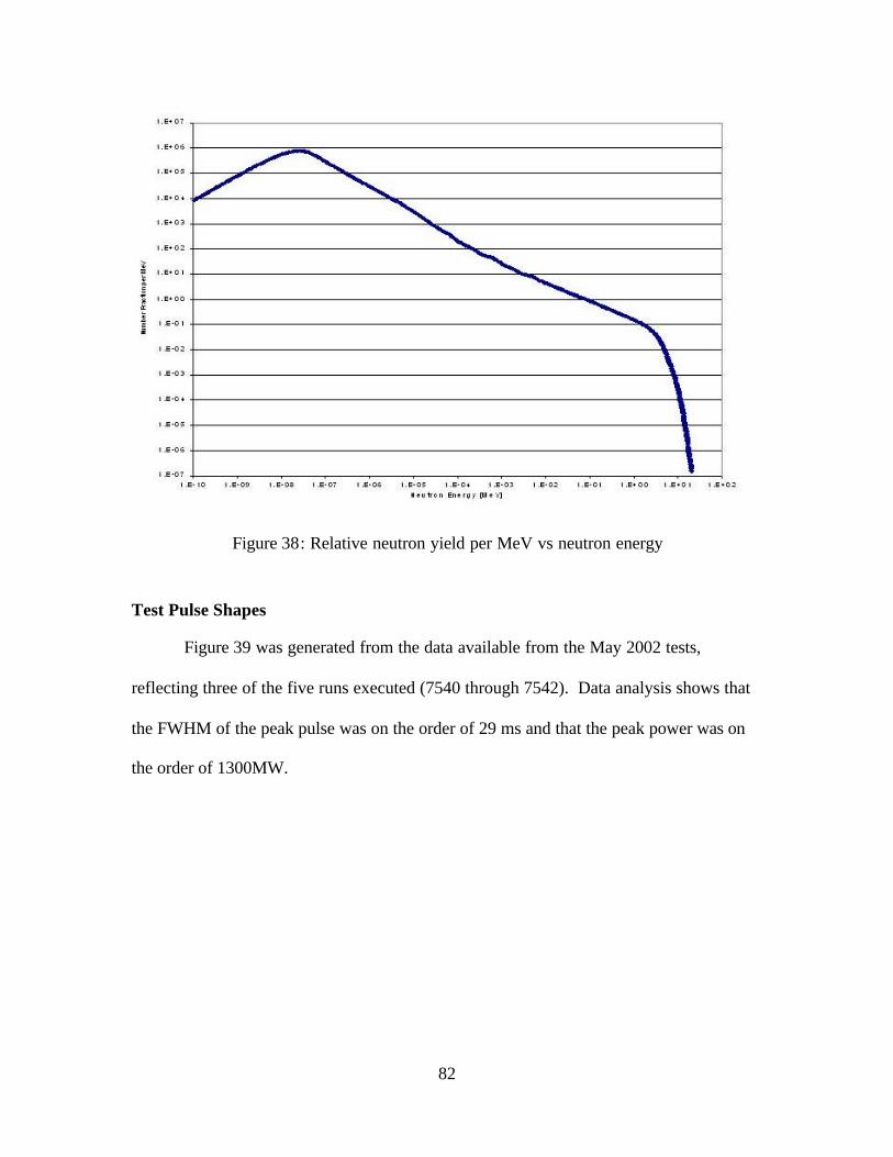
82
Figure 38: Relative neutron yield per MeV vs neutron energy
Test Pulse Shapes
Figure 39 was generated from the data available from the May 2002 tests,
reflecting three of the five runs executed (7540 through 7542). Data analysis shows that
the FWHM of the peak pulse was on the order of 29 ms and that the peak power was on
the order of 1300MW.
.(-» i-l-O- it-ft *>*•> B*ri/ t'4

83
Figure 39: Representative Sandia ACRR pulses (7540-7542)
Estimated Total Dose Delivered
In order to arrive at an estimated dose delivered to the test devices, the energy
yield curves were integrated over time, resulting in an average energy yield of 21.87 MJ.
By applying a neutron fluence normalization constant (3.5052x1014 cm-2 at 16.66 MJ)24
and dividing by the pulse width (123.2 ms) an estimated total neutron flux of 3.74x10¹⁵
cm-2 s-1 is obtained. Then, the standard dn/dE is obtained by multiplying the total flux by
the relative neutron yield given in Figure 38 and dividing each group by the average
group energy. The gamma dose is treated in a similar fashion, using a gamma dose
normalization constant of 197.8 KradSi at 16.66 MJ.

84
Using the same program used in the preliminary dosimetry calculations in Annex
A-3, an estimated neutron dose rate of 170 ± 10 MradSi per hour is obtained. This results
in a neutron total dose of 5.9 ± 0.4 KradSi and a gamma total dose of 260 ± 60 KradSi.

85
Appendix D. Sample Output Data
Raw Data
Figure 40 shows a representative raw data output file. As this file was produced
during the course of the gamma cell irradiation and the thermocouple was not used, no
temperature is given. For each chip, seven voltage sweeps were performed with the
specified parameters.
Figure 40: Representative raw data from output file

86
Parsed and Conditioned Data
As shown in Figure 41, the parsed and conditioned data files included the
following: the time elapsed in minutes, applied voltage in volts, measured current in
amperes, and the standard deviation in the measurement, also in amperes. The bottom
value in the figure of 999.0 indicates that the thermocouple was not used during this
particular measurement.
Figure 41: Representative parsed and conditioned data
Representative MathcadTM File
Figure 42 shows a portion of a representative Mathcad data manipulation file. As
shown in the figure, each measured current data point is first divided by the applied
voltage at which that measurement was taken in order to obtain the resistance. The initial
resistance as that voltage is then subtracted in order to obtain the difference. The change
in resistivity is then computed by dividing by the initial resistivity.

87
Figure 42: Representative MathcadTM data manipulation file
datal = IK9
C:\P10b.dat
I = rows(datal)
i=i266x 10^
n =0.1 1524 III =0 9
xl = datal , II 11,1
tl = datal 11,0
data2 = IS
C:\P9a.dat
12 = rows(data2)
n2 =0,1 12-1
x2 - = data2 - , ii2 ii2,l
t2 - = data2 - - ii2 ii2,0
yi ='f datal , = 0. ^.if "I datal -. datal
yi II7+I-I = if
11.2
data7
0,2
data3 =
r- IS
\P8a.dat
13 = rows(dala3)
n3 =0.1 I3I- I
ii3 n3.l
^
O - = data3 - - ii3 ii3,0
datal I datal| | datal , = 0 5. ^ ^.if
"I datal -. datal 11,2 1,2
11,1
11.1 2.1 .if datal - datal- -
11.2 2,2
datal 11,1
data7 -, , = 0. "^1 data7 117,2 ^^^^'0,2'
data7 - | dataL | data7 - , = 0 5. ^ ^.if
"'I data7 ^ .. datal ii7,2 1,2
data7 - | datal- | data7 - , = I. ^ —
"'' data7 - - datal- -

88
Bibliography
1 McCready, S. and T. Harlow, A. Heger, and K. Holbert. “Piezoresistive Micromechanical Transducer Operation in a Pulsed Neutron and Gamma Ray Environment.” Unpublished paper submitted to the IEEE Nuclear and Space Radiation Effects Conference, July 2002.
2 Bridgman, P.W. “The Effect of Homogeneous Mechanical Stress on the Electrical Resistance of Crystals.” Physical Review, Vol. 42, 15 December 1932.
3 Pfann, W.G. and R.N. Thurnston. “Semiconducting Stress Transducers Utilizing the Transverse and Shear Piezoresistance Effects.” Journal of Applied Physics. Vol. 32, No. 10. October, 1961.
4 Smith, Charles S. “Piezoresistance Effect in Germanium and Silicon.” Physical Review, Vol. 94. No 1, 1 April, 1954.
5 Mahan, Gerald D. Many-Particle Physics (2nd Edition). New York: Plenum Press, 1990.
6 Tandeske, Duane. Pressure Sensors:Selection and Application. New York: Marcel Dekker, Inc., 1991.
7 Patrick L. Walter.”Dynamic Force, Pressure, & Acceleration Measurement (Part 2)” Paper submitted to the Measurements and Controls Journal and provided on the Internet, http://www.endevco.com/main/literature/tutorials.html, June 1999.
8 Knudson, A.R. (et al). “The Effects of Radiation on MEMS Accelerometers.” IEEE Trans. Nucl. Sci. NS-43 3122 (1996).
9 Sze, S.E. Physics of Semiconductor Devices (2nd Edition). New York: John Wiley and Sons, 1981.
10 van Lint, V.A.J. Mechanisms of Radiation Effects in Electronic Materials, Volume 1. New York: John Wiley and Sons, 1980.
11 Yu, Z. (et al). PISCES-2ET and its Application Subsystems. Stanford: Stanford University, 1994.
12 Kraus, John D. and Daniel A. Fleisch. Electromagnetics with Applications (5th Ed.). Boston: McGraw-Hill, 1999.
13 Ma, T.P. and Paul V. Dressendorfer. Ionizing Radiation Effects in MOS Devices and Circuits. New York: John Wiley and Sons, 1989.
14 Messenger, George C. “A Summary Review of Displacement Damage from High Energy Radiation in Silicon Semiconductors and Semiconductor Devices.” IEEE Trans. Nucl. Sci. NS 39-469 (1992).

89
15 Werner, Matthias R. and Wolfgang R. Fahrner. “Review on Materials, Micro-sensors, Systems, and Devices for High-Temperature and Harsh-Environment Applications.” IEEE Trans. Nucl. Sci., NS-48, 249(2001).
16 Knudson, A.R. (et al). “The Effects of Radiation on MEMS Accelerometers.” IEEE Trans. Nucl. Sci. NS-43 3122 (1996).
17 Padgaonkar, Swarupa (et al). “Comparison of 14 MeV neutron- induced and 1 MeVelectron- induced radiation damage in crystalline silicon.” J. Phys.D: Appl. Phys. Vol. 24 (1991).
18 Lee, C.I (et al). “Total Dose Effects on Micro-mechanical Systems (MEMS): Accelerometers.” IEEE Trans. Nucl. Sci., NS-43 3127 (1996)
19 Janesick, James (et al). “Radiation Damage in Scientific Charge-Coupled Devices.” IEEE Trans. Nucl. Sci., NS-36 572 (1989).
20 Messenger, George C. and Milton S. Ash. The Effects of Radiation on Electronic Systems (2nd Edition). New York: Van Nostrand Reinhold, 1992.
21 Mottet, S. and A. Riozès. “Defect formation kinetics in irradiated silicon at 300K,” in Defects and Radiation Effects in Semiconductors, 1978. Ed. J.H. Albany. Bristol, U.K.: The Institute of Physics, 1979.
22 Gover, James E. Course handout, IEEE Nuclear and Space Radiation Effects Conference Short Course, Colorado Springs, July 1984.
23 Taylor, John R. An Introduction to Error Analysis: The Study of Uncertainties in Error Analysis. Mill Valley: University Science Press, 1982.
24 Griffin, Patrick, Research Associate, Sandia National Laboratories, Albuquerque, NM. Personal Correspondence, December 2002.
25 Kulite Semiconductor Products Inc. “XTE-190(M) Series and XTEL-190(M) Series.” Extract from product data sheet provided on the Internet. http://216.197.110.63/ pdfs/pdf_Data_Sheets/XTE.XTEL-190.pdf, December 2002.
26 Endevco Corp.“Model 7264B.” Extract from product data sheet provided on the Internet. http://www.endevco.com/data-sheets/72xx/7264B-500-2000.pdf, December 2002.
27 Talnagi, J. Senior Research Associate, Ohio State University Research Reactor Facility, Columbus OH. Personal Correspondence. November 2002.
28 NTE Electronics Inc. “NTE3041 Optoisolator NPN Transistor Output.” Extract from product data sheet provided on the Internet. http://www.nteinc.com/specs /3000to3099/pdf/nte3041.pdf September 2002.
29 Griffin, Patrick and others. “Characterization of ACRR Reference Benchmark Field.” Unpublished. December 2002.

90
Vita
Captain Samuel J. Willmon graduated from the United States Military Academy
at West Point, New York in 1994 with a Bachelor of Science degree in Physics.
Following his commissioning as a second lieutenant of Infantry, he was assigned to 1st
Battalion, 15th Infantry in Schweinfurt, Germany. While in Germany, he served as a rifle
platoon leader, mortar platoon leader, headquarters and headquarters company executive
officer, and battalion maintenance officer. During his tour in Germany, he spent six
months with Task Force 1-26, the Blue Spaders, in Bosnia-Herzogovina as part of IFOR,
CFOR, and later SFOR.
Following the Infantry Captain’s Career Course at Fort Benning, Georgia in 1999,
Captain Willmon was assigned as the assistant brigade operations officer for the 1st
Brigade, 2nd Infantry Division at Camp Casey, Korea. After ten months on brigade staff,
Captain Willmon assumed command of A Company, 2nd Battalion, 9th Infantry, also at
Camp Casey. In September 2001, he entered the Graduate School of Engineering at the
Air Force Institute of Technology at Wright-Patterson Air Force Base, Ohio. Upon
graduation, he will be assigned to the National Ground Intelligence Center.

REPORT DOCUMENTATION PAGE Form Approved OMB No. 074-0188
The public reporting burden for this collection of information is estimated to average 1 hour per response, including the time for reviewing instructions, searching existing data sources, gathering and maintaining the data needed, and completing and reviewing the collection of information. Send comments regarding this burden estimate or any other aspect of the collection of information, including suggestions for reducing this burden to Department of Defense, Washington Headquarters Services, Directorate for Information Operations and Reports (0704-0188), 1215 Jefferson Davis Highway, Suite 1204, Arlington, VA 22202-4302. Respondents should be aware that notwithstanding any other provision of law, no person shall be subject to an penalty for failing to comply with a collection of information if it does not display a currently valid OMB control number. PLEASE DO NOT RETURN YOUR FORM TO THE ABOVE ADDRESS.
1. REPORT DATE (DD-MM-YYYY) 25-03-2003
2. REPORT TYPE Master’s Thesis
3. DATES COVERED (From – To) Jun 2002 – Mar 2003
5a. CONTRACT NUMBER
5b. GRANT NUMBER
4. TITLE AND SUBTITLE TOTAL DOSE EFFECTS OF IONIZING AND NON-IONIZING RADIATION ON PIEZORESISTIVE PRESSURE TRANSDUCER CHIPS 5c. PROGRAM ELEMENT NUMBER
5d. PROJECT NUMBER ENP03-281 5e. TASK NUMBER
6. AUTHOR(S) Willmon, Samuel J., Captain, USA
5f. WORK UNIT NUMBER
7. PERFORMING ORGANIZATION NAMES(S) AND ADDRESS(S) Air Force Institute of Technology Graduate School of Engineering and Management (AFIT/EN) 2950 P Street, Building 640 WPAFB OH 45433-7765
8. PERFORMING ORGANIZATION REPORT NUMBER AFIT/GNE/ENP/03-11
10. SPONSOR/MONITOR’S ACRONYM(S)
9. SPONSORING/MONITORING AGENCY NAME(S) AND ADDRESS(ES) DTRA/CSNP Attn: Mr. Jerry Baird 2801 Telegraph Rd Alexandria, VA 22310 (703) 625-8128
11. SPONSOR/MONITOR’S REPORT NUMBER(S)
12. DISTRIBUTION/AVAILABILITY STATEMENT APPROVED FOR PUBLIC RELEASE; DISTRIBUTION UNLIMITED.
13. SUPPLEMENTARY NOTES 14. ABSTRACT The effects of ionizing and non-ionizing radiation on the resistivity of silicon-based, piezoresistive bulk micro-machined chips from pressure transducers were examined. Standard current-voltage (I-V) measurements were taken in-situ and post-irradiation during isothermal annealing at room temperature. One group of chips was irradiated to a maximum total gamma dose of 1MradSi in the 11,000 Ci 60Co gamma cell at Ohio State University. The second group of chips was irradiated at the Ohio State University Research Reactor facility to a maximum total neutron dose of 4 MradSi using beam port #1. The resistivity was shown to decrease during gamma irradiation as a result of Compton current generation and increase during neutron irradiation as a result of displacement damage. During irradiation in the gamma cell, the chips exhibited a 0.45 ± 0.19 % decrease in resistivity at saturation. During the neutron and gamma irradiation in the reactor, the chips exhibited a peak change in resistivity of 2.503 ± 0.003% at 2 MradSi, 3.055 ±0.002% at 3 MradSi, and 3.6921% (with unknown uncertainty) at 4 MradSi. Regardless of the total dose received, all chips demonstrated a permanent change in resistivity of 0.7697 ± 0.0006% at room temperature. 15. SUBJECT TERMS Piezoresistive, Transducer, Radiation, Damage mechanism
16. SECURITY CLASSIFICATION OF: 19a. NAME OF RESPONSIBLE PERSON James C. Petrosky, LTC, USA (ENP)
a. REPORT
U
b. ABSTRACT
U
c. THIS PAGE
U
17. LIMITATION OF ABSTRACT
UU
18. NUMBER OF PAGES
103
19b. TELEPHONE NUMBER (Include area code) (937) 255-6565, ext 4600; e-mail: [email protected]
Standard Form 298 (Rev. 8-98) Prescribed by ANSI Std. Z39-18
Copyright © 2022 FDOKUMEN