Cryogenic testing and multi-chip module design of a 31.3-45GHz MHEMT MMIC-based heterodyne receiver...
9
Cryogenic Testing and Multi-Chip Module Design of a 31.3-45GHz MHEMT MMIC-Based Heterodyne Receiver for Radio Astronomy Yuh-Jing Hwang a , Chau-Ching Chiong a , Su-Wei Chang a , Tashun Wei a , Wei-Ting Wong a , Yo-Shen Lin c , Ming-Tang Chen a , Huei Wang b and Hong-Yeh Chang c a Academia Sinica Institute of Astronomy and Astrophysics, P.O. Box 23-141, Taipei, 10671, Taiwan, R.O.C. b Department of Electrical Engineering and Institute of Communication Engineering, National Taiwan University, No. 1, Roosevelt Rd., Sec. 4, Taipei, 10671, Taiwan, R.O.C. c Department of Electrical Engineering, National Central University, No.300, Jhongda Rd., Jhongli City, Taoyuan County 32001, Taiwan, R.O.C. ABSTRACT A prototype Q-band millimeter-wave heterodyne receiver based on monolithic microwave integrated circuit (MMIC) chips is designed and tested. The MMIC chips, including two three-stage 31.3-45GHz low-noise amplifier (LNA), a diode balanced mixer and a 4-12GHz IF amplifier, are fabricated by a 0.15-um Gallium-Arsenide (GaAs) metamorphic high-electron mobility transistor (MHEMT) foundry service. The MMIC chips are measured by probe in the gain stage. The three-stage 31.3-45GHz LNA MMIC exhibits 31-35dB gain and 2.8-3.5dB noise figure under room temperature environment. The balanced diode mixer with 31.3-45.0GHz RF frequency range and 27.3-33GHz LO frequency range shows 10-13dB conversion loss under 10-dBm LO pumping over 4-12GHz IF frequency range. The LO power of the mixer is provided by a phase-locked GaAs hetero-junction bipolar transistor (HBT) MMIC voltage-controlled oscillator cascaded by a buffer amplifier. The packaged modules of the individual MHEMT MMIC receiver components are designed for testing under 15-20K cryogenic operating temperature to ensure the low-noise performance. A compact multi-chip receiver module design concept will be presented. Keywords: MHEMT, Q-band receiver, MMIC, HBT, VCO, Multi-Chip Module 1. INTRODUCTION The Ka-band (26.5-40GHz) and Q-band (33-50GHz) are one of the important atmospheric windows for lower frequency millimeter-wave astronomical observations. Many radio astronomy telescopes operated in millimeter-wavelength equipped with low-noise heterodyne receivers for these bands, including Very large Array (VLA) [1], Very Long Baseline Array (VLBA) [2], Green Bank Telescope (GBT) [3], Korean VLBI Network [4], VSOP [5], and Australia Telescope National Facility Compact Array [6]. The important scientific topics in these bands include high resolution Sunyaev-Zel’dovich effect imaging [7], cosmic microwave background, high-redshifted extragalactic CO lines [8] and probing magnetic field strength via Zeeman measurements [9-10]. Besides the existing millimeter-wave telescopes, the Atacama Large Millimeter-wave and Submillimeter-wave Array (ALMA) constructed on 5000-meter high-altitude plateau in Northern Chile will provide a much more powerful tool for observation. ALMA is an interferometer array composed by a baseline array with fifty 12-meter antennas, and a compact array with four 12-meters antennas and twelve 7-meter antennas. The receiver front-end system divided into 10 bands to cover the atmospheric windows with frequency range from 31.3 to 950GHz. The development of band 3, 4, 6, 7, 8, 9 are undergoing in several different astronomical institutions ____________________________________________________ Further author information – Yuh-Jing Hwang: [email protected] ASIAA Web: http://www.asiaa.sinica.edu.tw/ Millimeter and Submillimeter Detectors and Instrumentation for Astronomy IV edited by William D. Duncan, Wayne S. Holland, Stafford Withington, Jonas Zmuidzinas Proc. of SPIE Vol. 7020, 70201V, (2008) · 0277-786X/08/$18 · doi: 10.1117/12.789127 Proc. of SPIE Vol. 7020 70201V-1 2008 SPIE Digital Library -- Subscriber Archive Copy
-
Upload
independent -
Category
Documents
-
view
2 -
download
0
Transcript of Cryogenic testing and multi-chip module design of a 31.3-45GHz MHEMT MMIC-based heterodyne receiver...
Cryogenic Testing and Multi-Chip Module Design of a 31.3-45GHz MHEMT MMIC-Based Heterodyne Receiver for Radio Astronomy
Yuh-Jing Hwang a, Chau-Ching Chiong a, Su-Wei Chang a, Tashun Wei a, Wei-Ting Wong a, Yo-Shen Linc, Ming-Tang Chen a, Huei Wang b and Hong-Yeh Chang c
a Academia Sinica Institute of Astronomy and Astrophysics,
P.O. Box 23-141, Taipei, 10671, Taiwan, R.O.C.
b Department of Electrical Engineering and Institute of Communication Engineering, National Taiwan University, No. 1, Roosevelt Rd., Sec. 4, Taipei, 10671, Taiwan, R.O.C.
c Department of Electrical Engineering, National Central University, No.300, Jhongda Rd., Jhongli
City, Taoyuan County 32001, Taiwan, R.O.C.
ABSTRACT A prototype Q-band millimeter-wave heterodyne receiver based on monolithic microwave integrated circuit (MMIC) chips is designed and tested. The MMIC chips, including two three-stage 31.3-45GHz low-noise amplifier (LNA), a diode balanced mixer and a 4-12GHz IF amplifier, are fabricated by a 0.15-um Gallium-Arsenide (GaAs) metamorphic high-electron mobility transistor (MHEMT) foundry service. The MMIC chips are measured by probe in the gain stage. The three-stage 31.3-45GHz LNA MMIC exhibits 31-35dB gain and 2.8-3.5dB noise figure under room temperature environment. The balanced diode mixer with 31.3-45.0GHz RF frequency range and 27.3-33GHz LO frequency range shows 10-13dB conversion loss under 10-dBm LO pumping over 4-12GHz IF frequency range. The LO power of the mixer is provided by a phase-locked GaAs hetero-junction bipolar transistor (HBT) MMIC voltage-controlled oscillator cascaded by a buffer amplifier. The packaged modules of the individual MHEMT MMIC receiver components are designed for testing under 15-20K cryogenic operating temperature to ensure the low-noise performance. A compact multi-chip receiver module design concept will be presented. Keywords: MHEMT, Q-band receiver, MMIC, HBT, VCO, Multi-Chip Module
1. INTRODUCTION The Ka-band (26.5-40GHz) and Q-band (33-50GHz) are one of the important atmospheric windows for lower frequency millimeter-wave astronomical observations. Many radio astronomy telescopes operated in millimeter-wavelength equipped with low-noise heterodyne receivers for these bands, including Very large Array (VLA) [1], Very Long Baseline Array (VLBA) [2], Green Bank Telescope (GBT) [3], Korean VLBI Network [4], VSOP [5], and Australia Telescope National Facility Compact Array [6]. The important scientific topics in these bands include high resolution Sunyaev-Zel’dovich effect imaging [7], cosmic microwave background, high-redshifted extragalactic CO lines [8] and probing magnetic field strength via Zeeman measurements [9-10]. Besides the existing millimeter-wave telescopes, the Atacama Large Millimeter-wave and Submillimeter-wave Array (ALMA) constructed on 5000-meter high-altitude plateau in Northern Chile will provide a much more powerful tool for observation. ALMA is an interferometer array composed by a baseline array with fifty 12-meter antennas, and a compact array with four 12-meters antennas and twelve 7-meter antennas. The receiver front-end system divided into 10 bands to cover the atmospheric windows with frequency range from 31.3 to 950GHz. The development of band 3, 4, 6, 7, 8, 9 are undergoing in several different astronomical institutions
____________________________________________________ Further author information – Yuh-Jing Hwang: [email protected] ASIAA Web: http://www.asiaa.sinica.edu.tw/
Millimeter and Submillimeter Detectors and Instrumentation for Astronomy IVedited by William D. Duncan, Wayne S. Holland, Stafford Withington, Jonas ZmuidzinasProc. of SPIE Vol. 7020, 70201V, (2008) · 0277-786X/08/$18 · doi: 10.1117/12.789127
Proc. of SPIE Vol. 7020 70201V-12008 SPIE Digital Library -- Subscriber Archive Copy
worldwide [11-16]. However, it is believed that the ALM Band-1 which cover31.3-45GHz frequency range will be capable to solve the important scientific problems listed above. On the technical aspect, the main stream of the circuit fabrication process for the Ka and Q-band millimeter astronomical heterodyne receivers are the InP HEMT technology, such kind of technology provides the states-of-the-arts low-noise performance. However, the InP HEMT process has the limitation on high cost, low yield rate and low breakdown voltage. Recently, the innovation of the metamorphic HEMT technology reveals a possibility of similar performance as InP HEMT’s but avoid their limitations. In this paper, the initial effort on the development of the MHEMT MMIC circuits for Q-band radio astronomical heterodyne receiver is presented.
2. SYSTEM DESIGN CONSIDERATION The proposed heterodyne receiver is to cover the wid frequency coverage over the Q-band. The existing receivers with widest frequency coverage for this band are with 30-50GHz RF frequency range [6]. The ALMA band-1 receiver, which is in the same frequency range, set the RF frequency range to 31.3-45.0GHz. The work describe here is to aim the system specification similar ALMA Band-1, which is listed as follows [17] (1) RF Input Port: 31.3-45GHz. (2) LO input port: 27.3-33GHz, upper sideband (USB) mixing scheme. (3) IF output port: 4-12GHz. (4) Maximum receiver noise performance: 17K over 80% of the RF band, Single Side-Band; 28K at any RF frequency. (5) IF out put power: for load temperature between 10 and 800K at the RF input of the cartridge, total power in the IF
frequency range =-31dBm to -18dBm. For 290K RF input of the cartridge, power level in the IF frequency range =-30dBm/GHz.
(6) IF power variation: 6dB peak-to-peak in any 2GHz portion of the IF band. (7) 10 dB peak to peak across the complete IF band. (8) LO power requirement: minimum required mixer power = 5mW; for balanced, sideband- separating mixer, the
requirement = 10mW; LO power specification of 50% over worst case = 15mW. Based on the specifications, the receiver front-end block diagram is shown as Fig. 1. The key components of the receiver include the RF and IF low-noise amplifiers and the down-conversion mixer will be fabricated by MHEMT MMIC process. The noise and gain specifications of individual components are listed in Table I.
Table I Receiver Components Specification of the ALMA Band-1 Receiver Cartridge
Spec. - Any Frequency Spec. - 80% Frequency Gain (dB) Noise (K) Gain (dB) Noise (K)
Spillover and scattered 1.0 1.0 Window + Lens -0.05 -0.05 Corrugated Horn -0.1 -0.1
OMT -0.3 -0.2 1st-stage RF LNA 19.0 14.5 19.0 8.0 1st-stage Isolator -0.5 -0.5
2nd-stage RF LNA 19.0 17.0 19.0 12.0 2nd-stage Isolator -0.5 -0.5 Bandpass Filter -0.2 -0.2
Mixer -13.0 -13.0 IF amplifier 30.0 15.0 30.0 15.0
Receiver performance 53.35 22.85 53.35 14.85 IF output power (dBm) at
800K input load -17.1 -17.1
IF output power (dBm) at 10K input load -31.1 -32.2
Proc. of SPIE Vol. 7020 70201V-2

31.3-45.0GHz 31.3-45.0GHz 4.0-12.0GHz IFRF Low-Noise Baiidpass Mixer Low-Noise
Amplifiers Filters Amplifiers
DielectricLens
27.3-33.0GHzLO Signal
Fig. 1. Block diagram of the Q-band heterodyne receiver. In order to ensure low receiver noise temperature, the operating temperature of
the LNAs, mixers and bandpass filters are all keep in 20K cryogenic operating temperature.
3. DEVICES DEVELOPMENT AND TESTING The development of the key devices include the 30-50GHz low-noise amplifier, the broadband balanced diode mixer and the 4-12GHz IF amplifiers. A waveguide bandpass filter for 31.3-47GHz is also fabricated to fulfill the requirement of the upper side-band specification of the system. For other parts like the orthomode transducer, focusing lens and horn antenna, similar design has been developed by the ALMA partners [18]. A. MMIC Chips Development
The foundry service used for the MMIC chips development is a GaAs 0.15-µm gate length MHEMT process with 730mS/mm peak trans-conductance and 110GHz cutoff frequency [19]. The 30-50GHz low-noise amplifier, balanced diode mixer and the 4-12GHz IF amplifier are designed. The detail description of the circuit design and probe-rest results are described in [20]. Fig. 2 shows the MMIC chips of the 30-50GHz three-stage low-noise amplifier, balanced diode mixer. The size of both chip are 2000µm ×1000µm.
(a) (b)
Fig. 2. Examples of the MHEMT MMIC chips, (a) 30-50GHz three-stage low-noise amplifier, and (b) balanced diode mixer.
B. LNA Module Design and Testing
Due to the cryogenic testing requirement, the RF-frequency LNA circuit module design is with WR-22 input and output port. A Q-band transition probe is used for impedance transform from rectangular waveguide to microstrip, which is scaled from the W-band one developed by Leong et Al. [20]. The LNA MMIC chip is in the center of the LNA module bottom block with both RF input and output connected with the Q-band transition probes. The WR-22 rectangular waveguide is then bended by 90 degree to form in-line configuration. Fig. 3 shows the example of the packaged LNA module.
Proc. of SPIE Vol. 7020 70201V-3

F ciii1 I;1
\1_PI ..--i_ 7Jk
__
•
IL
Fig. 3. Mosaicing microscopic photograph of a packaged Q-band two-stage low-noise amplifier. Left and right side is the transition
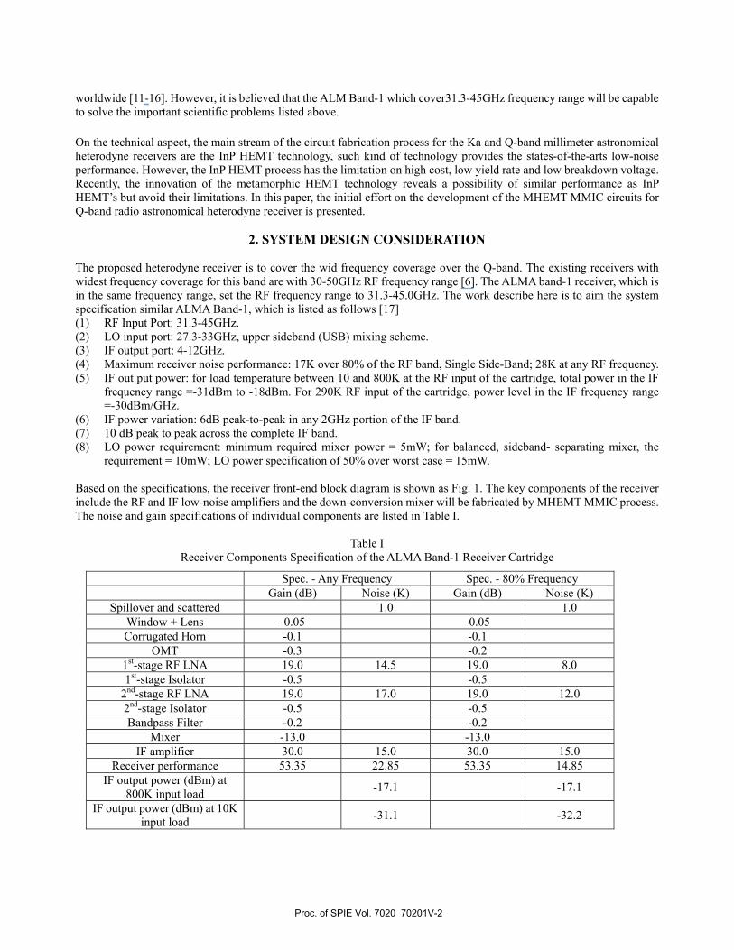
probe for microstrip to WR-22 rectangular waveguide. The LNA module is tested both under the room temperature and the cryogenic temperature. The goal of the room-temperature is to iterate the LNA stability, especially to remove the out-of-band oscillation problem due to the limited-area bias circuitry. The bias point for input /output matching and gain flatness optimization is also iterated. Small-signal scattering parameters are measured by phasor network analyzer. The forward gain is around 20-23dB over 32.5-45.0GHz.
(a) (b)
Fig. 4. Measurement arrange of the cryogenic small-signal scattering parameter measurement, (a) cryogenic test chamber with top cover opened and the device under test connected to the phasor network analyzer, (b) detail view of the low-noise amplifier inside the cryogenic chamber.
The cryogenic testing is implemented by a closed-cycle refrigerator with CTI-350 10K cold head to cool down to 20K. For small-signal scattering parameter measurement, the reference plan is set to the WR-22 waveguide interface to the LNA module, the calibration is implemented prior to the cool-down process. The measured arrangement is shown in Fig. 5. The measured results are shown in Fig. 6, It show that under the 20-K cryogenic environment, the forward gain of the amplifier is slightly increased than under the room-temperature environment, but the input/output impedance matching slightly changed.
Proc. of SPIE Vol. 7020 70201V-4
Mag
U
de
(dB)
Frequency (GHz)
Ma9a
U
de
Frequency (GHz)
Ma9n
U
de
(dB)
::
I E
I]j
E
-U-HI:E
I i
E
'E
32 34 26 36 aD 42 44 46 48 40
Frequency (GHz)
Magn
Ude
Frequency (GHz)
(a) (b)
(c) (d)
Fig. 5. Comparison of the small-signal scattering parameters results of the two-stage Q-band low-noise amplifier module illustrated in Fig. 3 measured at 20K cryogenic temperature (blue curve) and room-temperature environment (red curve), (a) forward gain (S21), (b) input matching (S11), (c) output matching(S22), and (d) reverse isolation(S12). The optimal bias settings under room temperature are Vd1=2.5V, Id1 = 16mA, Vd2 =1.0V, Id2 =15mA.
The noise temperature of the LNA is measured by using two differently approaches. The first approach uses a total power sensor to connect to the cryogenic amplifier output, with input with horn antenna. The second approach uses the simplified receiver arrangement with the first stage LNA in cryogenic environment only. A solid-state noise source is used as the hot load and the termination is used as the cold load. The detail noise temperature at given frequency can be measured by this approach. For both approach, the waveguide section from room-temperature flange to the cryogenic reference plane in front of the LNA is calibrated first. With the first approach, the overall noise temperature of the 2-stage amplifier shown in Fig. 3 is estimated. It show that the noise temperature is around 72K under 18K operating temperature. It is equivalent to 7dB noise figure based on 18K reference temperature, which show the circuit is with the same NF under room temperature. This result also indicates the noise performance is still far from the receiver specification requirement listed in Table I. One very important and serious problem on the LNA MMIC module testing is the low frequency oscillation and high-frequency, out-of-band oscillation. Lower frequency oscillation is typically introduced by the feedback loop by the bias network which can be easy suppressed by off-chip shunt capacitors. However, high-frequency, out-of-band oscillation is easily triggered in the LNA shown in Fig. 3. The measured frequency and power is typically 48.8GHz +9Bm. Suitable bias tuning and input impedance load should be carefully selected to suppress the high frequency oscillation.
C. Mixer Module Testing
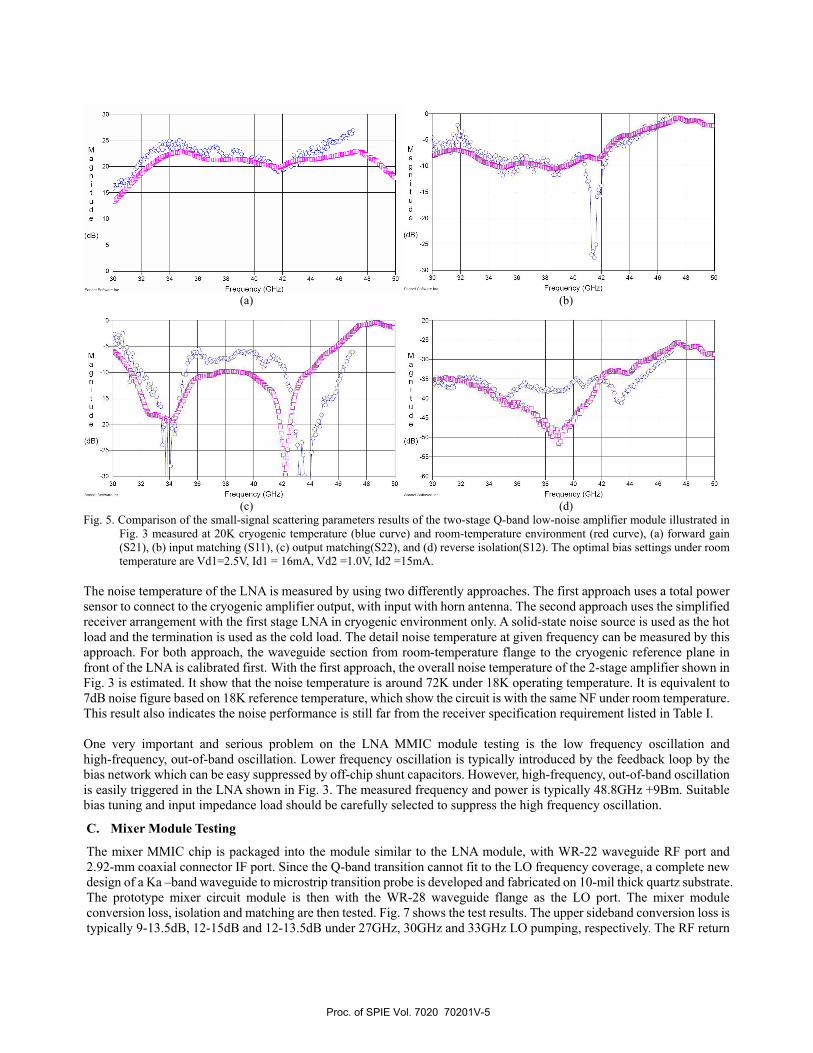
The mixer MMIC chip is packaged into the module similar to the LNA module, with WR-22 waveguide RF port and 2.92-mm coaxial connector IF port. Since the Q-band transition cannot fit to the LO frequency coverage, a complete new design of a Ka –band waveguide to microstrip transition probe is developed and fabricated on 10-mil thick quartz substrate. The prototype mixer circuit module is then with the WR-28 waveguide flange as the LO port. The mixer module conversion loss, isolation and matching are then tested. Fig. 7 shows the test results. The upper sideband conversion loss is typically 9-13.5dB, 12-15dB and 12-13.5dB under 27GHz, 30GHz and 33GHz LO pumping, respectively. The RF return
Proc. of SPIE Vol. 7020 70201V-5
Room-temperature 2nd stage RF LNA, 31.3-45.0GHZ bandpass filter, mixer, and IF
amplifier for down-conversion
Solid-statenoise source
-LO Signal
YIG narrowband tunable
bandpass filter
Upper Sideband Conversion Loss
+ f 27.00Hz, P 18.OdBrn
—U— f 30.00Hz, P 18.OdBm
f 33.00Hz, P 18.OdBm
30 32 34 36 38 40 42 44 46
RF Frequency (GHz)
M
(dB):ILIITI29 31 33 35 37 39 4 I 43 427
Frequency (GHz)
4 47
+ LO to IF Isolation—U— LO to RF Isolation
25 26 27 28 29 30 31 32 33 34 35
LO Frequency (GHz)
45
40
35
30
025020
C— 15
10
10
46 48
RF Frequency (GHz)
loss is typically less than -3dB, which introduce excess of the conversion loss and also degrade its flatness. LO-IF and LO-RF isolation is higher than 30dB. The results indicate that the optimal LO pumping is typically 18dBm, which is much higher than the expected value. Further iteration on the mixer MMIC design to improve RF matching and reduce the optimal LO power is required.
Fig. 6. Test arrangement of the 31.3-45.0GHz low-noise amplifier.
(a) (b)
(c) (d)
Fig. 7. Mixer performance test results, (a) upper sideband conversion loss with 4-12GHz IF passband, (b) RF matching under LO pumping at different frequencies, (c) LO to IF and LO to RF isolations, and (d) RF to LO isolation.
Proc. of SPIE Vol. 7020 70201V-6
SS
'S
-
S —- •- S S
• S
SI
D. Waveguide Bandpass Filter Fabrication and Testing
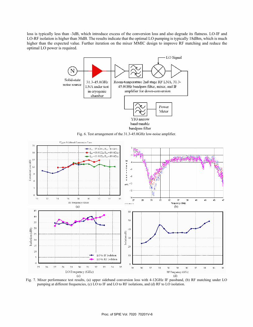
In order to fulfill the upper side-band requirement, several approaches of bandpass filters for 31.3-45GHz frequency range are designed [22]. The 9th-order WR-22 waveguide bandpass filter using capacitive iris is fabricated by machine shop using 4-piece block approach as shown in Fig. 6(a). The final assembled filter module is shown in Fig. 6(b). The measured scattering parameters of the fabricated prototype are shown in Fig. 6(c). The measured input and output return loss is lower than -20dB typically over the desired 31.3-45.0GHz pass band. The insertion loss is around -2.1dB at the lower edge and typically -0.3 to -0.5dB in the passband.
(a) (b)
(c)
Fig. 8. Prototype waveguide bandpsss filter, (a) the individual parts, (b) assembled module, and (c) measured scattering parameters.
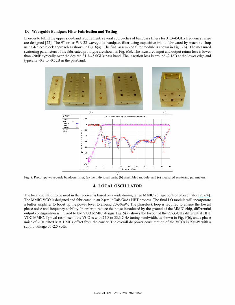
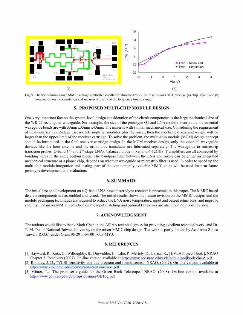
4. LOCAL OSCILLATOR The local oscillator to be used in the receiver is based on a wide-tuning range MMIC voltage controlled oscillator [23-24]. The MMIC VCO is designed and fabricated in an 2-µm InGaP-GaAs HBT process. The final LO module will incorporate a buffer amplifier to boost up the power level to around 20-30mW. The phaselock loop is required to ensure the lowest phase noise and frequency stability. In order to reduce the noise introduced by the ground of the MMIC chip, differential output configuration is utilized to the VCO MMIC design. Fig. 9(a) shows the layout of the 27-33GHz differential HBT VOC MMIC. Typical response of the VCO is with 27.8 to 33.3 GHz tuning bandwidth, as shown in Fig. 9(b), and a phase noise of -101 dBc/Hz at 1 MHz offset from the carrier. The overall dc power consumption of the VCOs is 90mW with a supply voltage of -2.5 volts.
Proc. of SPIE Vol. 7020 70201V-7
.1
IIfl..
r
CHII13VC j3 —33 3H12
=
OND • • VTGNI.
26
28
30
32
34
36
-2 -1 0 1 2 3 4Vtu (V)
Freq
. (G
Hz)
Freq. - MeasuredFreq. - Simulation
(a) (b)
Fig. 9. The wide-tuning range MMIC voltage controlled oscillator fabricated by 2-µm InGaP-GaAs HBT process, (a) chip layout, and (b) comparison on the simulation and measured results of the frequency tuning range.
5. PROPOSED MULTI-CHIP MODULE DESIGN
One very important fact on the system-level design consideration of the circuit components is the large mechanical size of the WR-22 rectangular waveguide. For example, the size of the prototype Q-band LNA module incorporate the essential waveguide bends are with 33mm x33mm x43mm, The mixer is with similar mechanical size. Considering the requirement of dual-polarization, 2-stage cascade RF amplifier modules plus the mixer, then the mechanical size and weight will be larger than the upper limit of the receiver cartridge. To solve the problem, the multi-chip module (MCM) design concept should be introduced in the final receiver cartridge design. In the MCM receiver design, only the essential waveguide devices like the horn antenna and the orthomode transducer are fabricated separately. The waveguide to microstrip transition probes, Q-band 1st- and 2nd-stage LNAs, balanced diode mixer and 4-12GHz IF amplifiers are all connected by bonding wires in the same bottom block. The bandpass filter between the LNA and mixer can be either an integrated mechanical structure or a planar chip, depends on whether waveguide or microstrip filter is used. In order to speed up the multi-chip module integration and testing, part of the commercially available MMIC chips will be used for near future prototype development and evaluation.
6. SUMMARY
The initial test and development on a Q-band LNA based heterodyne receiver is presented in this paper. The MMIC based discrete components are assembled and tested. The initial results shows that future revision on the MMIC designs and the module packaging techniques are required to reduce the LNA noise temperature, input and output return loss, and improve stability. For mixer MMIC, reduction on the input matching and optimal LO power are also main points of revision.
7. ACKNOWLEDGMENT The authors would like to thank Mark Chen in the ASIAA technical group for providing excellent technical work, and Dr. T.-M. Tsai in National Taiwan University on the mixer MMIC chip design. The work is partly funded by Academia Sinica Taiwan, R.O.C. under Grant 96-2911-M-001-005-MY3.
8. REFERENCES [1] Hayward, R., Kutz, C., Willoughby, B., Dinwiddie, H., Lilie, P., Mertely, D., Latasa, R., [ EVLA Project Book ], NRAO
Chapter 5: Receivers (2007). On-line version available at http://www.aoc.nrao.edu/evla/admin/projbook/chap5.pdf [2] Romney, J. D., “VLBI sensitivity upgrade program and memo series,” NRAO, (2007). On-line version available at
http://www.vlba.nrao.edu/memos/sensi/sensimemo1.pdf [3] Minter, T., “The proposer’s guide for the Green Bank Telescope,” NRAO, (2008). On-line version available at
http://www.gb.nrao.edu/gbtprops/obsman/GBTog.pdf
Proc. of SPIE Vol. 7020 70201V-8
[4] Han, S. -T., Lee, J.-W., Kang, H. Je, J., D., Chung, M.-H., Wi, S.-O., Sasao, T., Wylde, R., “Millimeter-wave receiver optics for Korean VLBI Network,” Int. J. Infrared Milli. Waves, 29(1), 67-78, (2008).
[5] Hirabayashi, H., Murata, Y., Asaki, Y., Edwards, P. G., Mochizuki, N., Natori, M. C., Inoue, M., Umemoto, T., Kameno, S., Kono, Y., Tsuboi, M., and Kasuga, T., “The VSOP-2 Project: a second-generation space-VLBI mission ranging to mm-wavelengths,” Proc. SPIE 5487, 1646-1656 (2004).
[6] Moorey, G., Gough, R., Graves, G., Leach, M., Sinclair, M., Bolton, R., Bowen, M., Kanoniuk, H., Reilly, L., and Jackson, S., “Australia Telescope millimetre wave receiver system,” Workshop on the Applications of Radio Science, 20-22 (2002).
[7] Carlstrom, J. E., Joy, M., Grego, L., Holder, G., Holzapfel, W. L., LaRoque, S., Mohr, J. J., and Reese, E. D., “The Sunyaev-Zel'dovich Effect: Results and Future Prospects,” Proc. IAP conference on Constructing the Universe with Clusters of Galaxies, (2000).
[8] Tsuboi, M. and Nakai, N., “Observations of CO (J = 1-0) and (J = 3-2) emission lines toward the very high-redshifted galaxy IRAS F10214+4724,” Publications of the Astronomical Society of Japan, 44(6) L241-L245 (1992).
[9] Crutcher, R. M., “Magnetic Fields in Molecular Clouds: Observations Confront Theory,” ApJ., 520, 706-713(1999). [10] Modjaz, M., Moran, J. M., Kondratko, P. T., and Greenhill, L. J., “Probing the Magnetic Field at Subparsec Radii in
the Accretion Disk of NGC 4258,” ApJl, 626, 104–119 (2005). [11] Claude, S. , Dindo, P., Erickson, D., Jiang, F., Yeung, K., Derdall, D., Duncan, D., Garcia, D., Henke, D., Leckie, B.,
Lichtenberger, A., Niranjanan, P., Pan, S.-K., Pfleger, M., Rodrigues, G., Szeto, K., Welle, P., and Caputa, K., “The Band 3 receiver (84-116 GHz) for ALMA, Proc.IRMMW-THz 2005, 2, 407- 408 (2005).
[12] Ogawa, H., Yonekura, Y., Asayama, S., Kimura, K., Mizuno, A., Mizuno, N., Minamidani, T., Maeda, H., Suzuki, K., Fukui, Y., Andoh, H., Sekimoto, Y., and Noguchi, T., “ALMA Front-End System for Band 4,” Proc. IAU 8th Asian-Pacific Regional Meeting, II, 23-24 (2002).
[13] Kerr, A., Pan, S.-K., Lauria, E. F., Lichtenberger, A. W., Zhang, J., Pospieszalski, M. W., Horner, N., Ediss, G. A., Effland, J. E., Groves, R. L., “The ALMA Band 6 (211-275GHz) sideband separating SIS mixer-preamplifier,” Proc. 15th Int. Symp. Space Terahertz Tech, 55-61(2004).
[14] Claude, S., “Sideband-Separating SIS Mixer For ALMA Band 7, 275-370 GHz,” Proc. 14th Int. Symp. Space Terahertz Tech, (2003).
[15] Shan, W., Asayama, S., Kamikura, M., Noguchi, T., Shi, S., Sekimoto, Y., “A 380-500GHz low noise superconductor- insulator-superconductor mixer for ALMA Band-8,” IEICE Trans. Electron., E89-C(2), 170-176 (2006).
[16] Baryshev, A. M., Hesper, R., Jackson, B. D., Mena, P., Barkhof, J., Zijstra, T., Lodewijk, C., Gerlofsma, G., Adema, J., Rivas, R., Keizer, K., Bekema, M., Koops, A., Wild, W., Klapwijk, T. M., “Design and performance of the 600-720 GHz ALMA band 9 cartridge,” Proc. IRMMW-THz 2005, (1), 70- 71 (2005).
[17] G. A. Ediss, J. Webber, G. H. Tan, “Front-end test and measurements specifications,” Atacama Large Millimeter Array Internal Documents, #FEND-40.09.03.00-003-A-SPE, (2005).
[18] M. Carter and R. Nesti, “ALMA front end optics design report, Appendix I, Band 1 optics measurements” Atacama Large Millimeter Array Internal Documents, #FEND-40.02.00.00-035-B-REP, (2007).
[19] WIN Semiconductor Corporation. http://www.winfoundry.com/ [20] Weng, S.-H., Lin, C.-H., Chang, H.-Y., and Chiong, C.-C., “Q-band low noise amplifiers using a 0.15-µm MHEMT
process for broadband communication and radio astronomy applications,” 2008 IEEE MTT-S Intl. Microwave Symp. Digest (2008).
[21] Leong, Y.-C. and Weinreb, S., “Full band waveguide-to-microstrip probe transitions,” 1999 IEEE MTT-S Intl. Microwave Symp. Digest, (4), 1435-1438 (1999).
[22] Hsieh, Y.-S., “Millimeter-wave bandpass filter designs for K-band and Q-band applications,” Master thesis, Department of Electrical Engineering, National Central University (2008).
[23] Chiong, C.-C., Chang, H.-Y. and Chen, M.-T., “Ka-Band Wide-Bandwidth Voltage-Controlled Oscillators in InGaP- GaAs HBT Technology,” Proc. 3rd European Microwave Integrated Circuit Conference, (2008).
[24] Chiong, C.-C., Chang, H.-Y., and Chen, M. T., “Wide-Bandwidth InGaP-GaAs HBT Voltage-Controlled Oscillators in K- and Ku-Band,” Proc. Global Symp. Millimeter Wave (GSMM), 185-188 (2008).
Proc. of SPIE Vol. 7020 70201V-9