Test procedures handbook for surveillance receivers below ...

IEEE TRANSACTIONS ON MICROWAVE THEORY AND TECHNIQUES, VOL. 54, NO. 6, JUNE 2006 2301
Development of Integrated HEB/MMIC Receiversfor Near-Range Terahertz Imaging
Fernando Rodriguez-Morales, Student Member, IEEE, K. Sigfrid Yngvesson, Life Fellow, IEEE, Richard Zannoni,Eyal Gerecht, Member, IEEE, Dazhen Gu, Student Member, IEEE, Xin Zhao, Niklas Wadefalk, and
John J. Nicholson
Abstract—We present measurement results for a new type ofintegrated terahertz receiver, as an extension to previous work bythe authors. The receiver we developed integrates quasi-opticallycoupled phonon-cooled NbN hot electron bolometric (HEB) mixersin close proximity with InP monolithic microwave integrated cir-cuit (MMIC) intermediate-frequency (IF) amplifiers. We havemeasured antenna radiation pattern, receiver noise temperature,and bandwidth, as well as short-term stability of the integratedreceivers. The measurements were performed at 1.6 and 2.5 THzover a very broadband IF frequency range. We have been able toextend the effective bandwidth of these receivers up to 5 GHz, thewidest reported for any integrated configuration operating above1 THz. The suitability of the HEB/MMIC approach for imagingapplications has been confirmed through the development of aprototype system for near-range scanning. The results presentedhere are very promising for the future development of heterodynefocal plane arrays for space-based receivers, medical applications,and surveillance.
Index Terms—Focal plane arrays, hot electron bolometric(HEB) mixers, imaging, integrated terahertz receivers, monolithicmicrowave integrated circit (MMIC) low-noise amplifiers (LNAs).
I. INTRODUCTION
THE terahertz frequency range is loosely defined as the re-gion of frequencies between 300 GHz and 3 THz. This part
of the electromagnetic spectrum has traditionally found variousimportant applications for high-resolution spectroscopy. Theseapplications include earth, planetary, and space science. Morerecently, medical and surveillance imaging systems have beenunder development [1].
A number of coherent detector technologies has been devel-oped over the past two decades to fulfill the requirements forlow-noise receivers operating in the terahertz regime. Amongthese technologies we encounter Schottky diode mixers, super-conducting-insulating-superconducting (SIS) junctions, and su-perconducting hot electron bolometric (HEB) mixers. Each ofthese technologies has inherent advantages and shortcomings.
Manuscript received October 8, 2005; revised February 20, 2006. This workwas supported by NASA through the Langley Research Center under ContractNAS1-01058 and by CONACyT, Mexico.
F. Rodriguez-Morales, K. S. Yngvesson, R. Zannoni, E. Gerecht, D. Gu,X. Zhao, and J. J. Nicholson are with the Department of Electrical andComputer Engineering, University of Massachusetts at Amherst, Amherst,MA 01002 USA.
N. Wadefalk was with the RF and Microwave Group, California Institute ofTechnology, Pasadena, CA 91125 USA. He is now with the Microwave Elec-tronics Laboratory Group, Chalmers University of Technology, SE-412 96 Göte-borg, Sweden.
Digital Object Identifier 10.1109/TMTT.2006.875257
For example, Schottky diode mixers are inexpensive to fabricateand do not necessarily require operation in a cryogenic environ-ment; however, they present a high local oscillator (LO) powerconsumption (on the order of 1 mW) and a limited noise perfor-mance. SIS mixers have a remarkable noise performance below1.2 THz, but their sensitivity degrades very quickly beyond thatfrequency due to fundamental limitations. HEB mixers have thelowest noise performance for frequencies above 1 THz, in ad-dition to having low LO power consumption (on the order of1 W), but the models that describe their behavior are yet tobe completed. Still, HEB mixers represent the most promisingtechnology for heterodyne detection beyond 1 THz.
In its most general configuration, a terahertz heterodynereceiver is composed of an active mixing element in cascadewith a cryogenic low-noise amplifier (LNA) for the interme-diate-frequency (IF) output. The available technologies for IFLNAs have evolved over time from GaAs field-effect transistorsto high electron mobility transistors (HEMTs) [2], the currentworkhorse devices of the microwave/millimeter-wave world[3]–[5]. Moreover, advances in fabrication technologies andcircuit modeling have made possible the advent of monolithicmicrowave integrated circuit (MMIC) LNAs. HEMT MMICLNAs provide outstanding noise performance and very lowdc-power consumption, with the additional advantage of re-duced physical size [6]–[8].
In the aforementioned receiver configuration, the mixing el-ement and the IF LNA (whether MMIC or not) are typically in-dependent units connected by means of a coaxial transmissionline. A cryogenic isolator is often added to the receiver chainin order to minimize standing waves between the mixer and theIF LNA and to guarantee the unconditional stability of the IFamplifier [Fig. 1(a)]. Currently available isolators occupy con-siderable physical space, increase the thermal load, and limitthe receiver IF bandwidth to not more than an octave. The re-ceiver arrangement as illustrated in Fig. 1(a) works well in mostcases; in fact, several instruments designed for astrophysical ob-servations are based on this configuration [9], [10]. Neverthe-less, the development of terahertz heterodyne detectors has longcalled for receiver integration (and thus size reduction), a trendshared by most modern electronic circuits. Receiver miniatur-ization represents a significant advantage, especially for mul-tiple receiver systems such as focal plane arrays (FPAs).
Significant progress has been made in this quest for com-pactness in submillimeter-wave receivers. One of the earliestconceptual arrays that suggested the use of terahertz detectorsin close proximity with LNAs was described in [11]. The firstintegrated receiver based on an SIS junction and an HEMT IF
0018-9480/$20.00 © 2006 IEEE

2302 IEEE TRANSACTIONS ON MICROWAVE THEORY AND TECHNIQUES, VOL. 54, NO. 6, JUNE 2006
Fig. 1. Quasi-optical terahertz receivers: (a) traditional single-element receiver configuration and (b) integrated single-element receiver configuration.
amplifier was reported for 270 GHz in [12]. Later, a fully inte-grated array based on SIS mixers, superconducting quantum in-terference device (SQUID) IF amplifiers, and a superconductingJosephson-type LO was demonstrated at 500 GHz in [13]. Theintegration of HEB mixers and (GaAs) MMIC IF amplifiers wasfirst proposed in [14], but it was not until several years later thatsuch integration was actually implemented for a 1.6 THz focalplane array, using NbN HEBs and InP MMIC LNAs [15], [16].
In this paper, we extend [15] and [16] by presenting an ex-tensive set of measurements performed on several NbN mixers,using the HEB/MMIC integrated approach. We have character-ized antenna radiation pattern, optical coupling efficiency, re-ceiver noise temperature, receiver IF bandwidth, and gain sta-bility. Some of the measurements were performed for more thanone local oscillator frequency. Furthermore, we describe the im-plementation of a prototype scanning system for near-range ter-ahertz imaging. A similar imaging system has been recentlyreported for 640 GHz, using Schottky diode mixers [17]. Thesystem we present operates at 1.6 THz and utilizes an HEB/MMIC receiver. The prototype is in the development stage andwill undergo several improvements; however, preliminary re-sults are in conformity with our design considerations.
This paper is organized as follows. Section II provides anoverview of the design details for the integrated HEB/MMICconfiguration. Section III describes the parameters measuredand their importance for the optimum receiver operation. Anoutline of the laboratory setups and the experimental results arepresented in Section IV. Section V discusses the implementa-tion of the prototype scanning imager. A brief comparison ofHEB/MMIC receivers with competing direct detectors is alsogiven in Section V. Section VI addresses some considerationsfor the construction of large HEB/MMIC arrays, including is-sues pertaining to field deployment.
II. HEB/MMIC RECEIVER OVERVIEW
The configuration for the integrated receiver we have de-veloped is shown in Fig. 1(b). The active mixer elements arephonon-cooled NbN HEB mixers fabricated on silicon sub-strates. The device chip size is mm mm m. Devicedimensions are typically 4 m wide by 0.5 m long. The core ofthe HEB devices we use is the thin NbN superconducting film
produced at Moscow State Pedagogical University, Moscow,Russia. The device fabrication was performed through collabo-ration with the National Institute of Standards and Technologyat Boulder, CO, and Chalmers University of Technology,Göteborg, Sweden. The HEB mixers are integrated with planartwin-slot antennas or log-periodic antennas. Twin-slot antennasare narrow bandwidth and linearly polarized. Log-periodicantennas are broadband and the angle of polarization that yieldsthe best response varies with frequency, depending upon thegeometry of the teeth. The design center frequency of the twotypes of antennas we use throughout this paper is 1.6 THz.However, as will be shown, this technology can operate at sig-nificantly higher terahertz frequencies by properly scaling theantenna dimensions. We have chosen a quasi-optical scheme forradiation coupling, in which a 4-mm-diameter silicon ellipticallens is used in conjunction with the monolithic antenna.
The IF chain of the integrated receiver is composed of anInP MMIC LNA and additional microwave circuitry. TheMMIC chips we use (size 0.75 2 mm) have been developedby Weinreb and Wadefalk at the Jet Propulsion Laboratory,California Institute of Technology [18], [19]. The chips wereoriginally intended for use on the Allen telescope array [20].These amplifiers have three 0.1 m InP HEMT stages. Theyprovide a high gain (up to 32 dB), remarkably low noise (lessthan 8 K over the band with a minimum of 3.5 K), and verybroadband performance (0.5–11 GHz). An important featureof these chips is the possibility of adjusting the bias settings tominimize dc-power utilization. This adjustment can be madewithout significantly affecting the overall amplifier perfor-mance. The best noise conditions are obtained with 20 mWof power dissipation. The best tradeoff among sufficient gain,low power, and low-noise performance is achieved with onlyabout 5 mW (Fig. 2). Low power consumption is particularlyimportant for multipixel receiver systems.
In order to minimize the noise figure of the integrated re-ceiver, the matching between the HEB mixer output and theMMIC input had to be optimized. This optimization requireda knowledge of the HEB IF impedance as well as the optimalsource impedance needed for the low-noise operation of theMMIC. The optimal source impedance of the amplifier wasobtained using computer simulations and measurements. In

RODRIGUEZ-MORALES et al.: DEVELOPMENT OF INTEGRATED HEB/MMIC RECEIVERS FOR NEAR-RANGE TERAHERTZ IMAGING 2303
Fig. 2. Measured performance of the MMIC low-noise amplifier used in ourreceivers. A microstrip matching transformer was used at the input of the MMICin order to yield minimum noise figure. The measurements were performed atan operating temperature of 11 K.
regards to the HEB mixer impedance, careful measurementshave been carried out on custom-made NbN devices [16], [21].These studies showed that the appropriate combination of LOpower and dc bias leads to a mixer impedance dominated bythe real part and close to the dc differential resistance .The foregoing approximation holds for operating points nearthe optimum (lowest noise) and for frequencies below the IFnoise bandwidth of the HEB mixer.1 The imaginary part of theHEB impedance has been taken into account in our computersimulations as a small (though not negligible) reactance. Withthese considerations, it has been possible to accomplish abroadband coupling between the MMIC LNA and the HEB.This was achieved by employing a multisection microstripmatching transformer. This circuit provides a near-optimumreflection coefficient to the input of the MMIC while presentingan impedance close to 50 as seen at the HEB terminals.Optimal noise operation of the MMIC is thus achieved whenthe dc differential resistance of the HEB is adjusted to be 50 .However, can be as high as 95 at the optimum oper-ating point for the mixer, in which case the noise temperatureof the LNA will still be sufficiently low.
The microstrip matching transformer also eliminates the needfor an isolator (which drastically reduces the size). All the re-quired dc-bias networks are built on separate circuit boards andplaced inside the integrated receiver module. The MMIC ampli-fier is enclosed in a narrow rectangular cavity in order to sup-press undesired waveguide modes that could drive it into os-cillation. The cavity is designed to have a cutoff frequency of75 GHz, which is well above the maximum frequency of opera-tion of the MMIC. A photograph of the HEB/MMIC integratedreceiver is shown in Fig. 3. A simplified circuit diagram of the
1The IF noise bandwidth is defined as the frequency at which the receivernoise temperature doubles with respect to the low-frequency value. This param-eter will be later denoted asB . A well-known feature of phonon-cooled HEBsis that B is typically (two times) wider than the conversion gain bandwidth[14].
Fig. 3. Inside view of the integrated quasi-optical HEB/MMIC receiver. Theantenna shown in this picture corresponds to a twin-slot design.
Fig. 4. Simplified circuit diagram of the integrated HEB/MMIC receiver. TheMMIC LNA is biased with a common gate and a common drain voltage for allstages.
integrated receiver is shown in Fig. 4. C1 and L1 form a bias-teewith broadband performance for the HEB mixer.
The integrated receiver is operated at 4 K, inside a liquid he-lium (LHe) cryostat. The LO source we use is a laser-pumped far infrared (FIR) gaseous laser system. Although solid-state sources with sufficiently high power have become recentlyavailable [22]–[24], an FIR laser system is very well suited forextensive laboratory testing. Our system produces stable contin-uous-wave (CW) terahertz radiation with an output power up toabout 100 mW. The LO laser can be readily tuned to differentfrequencies by changing the gas in the FIR tube. A mylar beamsplitter with a thickness of 6 m is used as diplexer betweenthe LO and the signal beam. Two different LO laser frequenciesare used for this paper: 1.63 and 2.5 THz. The 1.63 THz laserline runs on difluoromethane gas while the 2.5 THz line runs onmethanol gas.
III. RECEIVER CHARACTERIZATION
As a first step for the validation of the HEB/MMIC approach,we conducted a variety of tests on different NbN mixer devices.A description of the different parameters that were measuredand the relevance they have to this investigation is outlined next.
2304 IEEE TRANSACTIONS ON MICROWAVE THEORY AND TECHNIQUES, VOL. 54, NO. 6, JUNE 2006
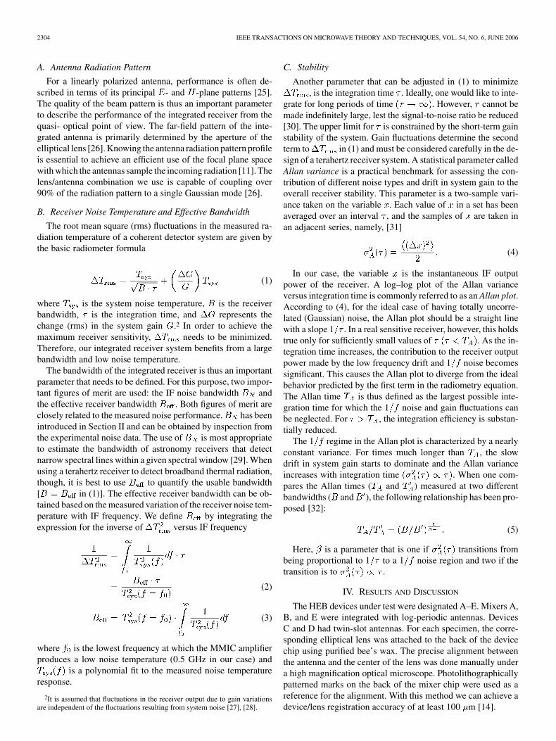
A. Antenna Radiation Pattern
For a linearly polarized antenna, performance is often de-scribed in terms of its principal - and -plane patterns [25].The quality of the beam pattern is thus an important parameterto describe the performance of the integrated receiver from thequasi- optical point of view. The far-field pattern of the inte-grated antenna is primarily determined by the aperture of theelliptical lens [26]. Knowing the antenna radiation pattern profileis essential to achieve an efficient use of the focal plane spacewith which the antennas sample the incoming radiation [11]. Thelens/antenna combination we use is capable of coupling over90% of the radiation pattern to a single Gaussian mode [26].
B. Receiver Noise Temperature and Effective Bandwidth
The root mean square (rms) fluctuations in the measured ra-diation temperature of a coherent detector system are given bythe basic radiometer formula
(1)
where is the system noise temperature, is the receiverbandwidth, is the integration time, and represents thechange (rms) in the system gain .2 In order to achieve themaximum receiver sensitivity, needs to be minimized.Therefore, our integrated receiver system benefits from a largebandwidth and low noise temperature.
The bandwidth of the integrated receiver is thus an importantparameter that needs to be defined. For this purpose, two impor-tant figures of merit are used: the IF noise bandwidth andthe effective receiver bandwidth . Both figures of merit areclosely related to the measured noise performance. has beenintroduced in Section II and can be obtained by inspection fromthe experimental noise data. The use of is most appropriateto estimate the bandwidth of astronomy receivers that detectnarrow spectral lines within a given spectral window [29]. Whenusing a terahertz receiver to detect broadband thermal radiation,though, it is best to use to quantify the usable bandwidth[ in (1)]. The effective receiver bandwidth can be ob-tained based on the measured variation of the receiver noise tem-perature with IF frequency. We define by integrating theexpression for the inverse of versus IF frequency
(2)
(3)
where is the lowest frequency at which the MMIC amplifierproduces a low noise temperature (0.5 GHz in our case) and
is a polynomial fit to the measured noise temperatureresponse.
2It is assumed that fluctuations in the receiver output due to gain variationsare independent of the fluctuations resulting from system noise [27], [28].
C. Stability
Another parameter that can be adjusted in (1) to minimize, is the integration time . Ideally, one would like to inte-
grate for long periods of time . However, cannot bemade indefinitely large, lest the signal-to-noise ratio be reduced[30]. The upper limit for is constrained by the short-term gainstability of the system. Gain fluctuations determine the secondterm to in (1) and must be considered carefully in the de-sign of a terahertz receiver system. A statistical parameter calledAllan variance is a practical benchmark for assessing the con-tribution of different noise types and drift in system gain to theoverall receiver stability. This parameter is a two-sample vari-ance taken on the variable . Each value of in a set has beenaveraged over an interval , and the samples of are taken inan adjacent series, namely, [31]
(4)
In our case, the variable is the instantaneous IF outputpower of the receiver. A log–log plot of the Allan varianceversus integration time is commonly referred to as an Allan plot.According to (4), for the ideal case of having totally uncorre-lated (Gaussian) noise, the Allan plot should be a straight linewith a slope 1 . In a real sensitive receiver, however, this holdstrue only for sufficiently small values of . As the in-tegration time increases, the contribution to the receiver outputpower made by the low frequency drift and 1 noise becomessignificant. This causes the Allan plot to diverge from the idealbehavior predicted by the first term in the radiometry equation.The Allan time is thus defined as the largest possible inte-gration time for which the 1 noise and gain fluctuations canbe neglected. For , the integration efficiency is substan-tially reduced.
The 1 regime in the Allan plot is characterized by a nearlyconstant variance. For times much longer than , the slowdrift in system gain starts to dominate and the Allan varianceincreases with integration time . When one com-pares the Allan times ( and ) measured at two differentbandwidths ( and ), the following relationship has been pro-posed [32]:
(5)
Here, is a parameter that is one if transitions frombeing proportional to 1 to a 1 noise region and two if thetransition is to .
IV. RESULTS AND DISCUSSION
The HEB devices under test were designated A–E. Mixers A,B, and E were integrated with log-periodic antennas. DevicesC and D had twin-slot antennas. For each specimen, the corre-sponding elliptical lens was attached to the back of the devicechip using purified bee’s wax. The precise alignment betweenthe antenna and the center of the lens was done manually undera high magnification optical microscope. Photolithographicallypatterned marks on the back of the mixer chip were used as areference for the alignment. With this method we can achieve adevice/lens registration accuracy of at least 100 m [14].

RODRIGUEZ-MORALES et al.: DEVELOPMENT OF INTEGRATED HEB/MMIC RECEIVERS FOR NEAR-RANGE TERAHERTZ IMAGING 2305
A. Antenna Radiation Pattern
These measurements were completed at 1.6 THz and onlyfor twin-slot antenna devices. Results for the log-periodic ver-sion have been reported in earlier work by Ji [33]. The HEBswere operated as direct detectors for these measurements. Werequired the use of a special fixture instead of the integratedmixer block. This is justified since the quasi-optical part of thereceiver remained unchanged after the optical test. The oper-ating temperature of the device under test was increased to 8 K(just below the critical temperature of the superconducting NbNfilm) using a power resistor heater. This step was done in orderto achieve maximum sensitivity. The laser beam was used as aninput source and scanned vertically (for the -plane) and hor-izontally (for the -plane). The output voltage (after pream-plification) was continually recorded from a lock-in amplifierusing its general-purpose interface bus (GPIB) port and a Lab-View program. To accomplish the beam scanning, we used a ro-tating mirror mounted on a special translation unit. The mirrorsteered the beam with small angular increments while keeping itfocused in the aperture plane of the elliptical lens. The FIR beamwas chopped by means of an acoustooptical modulator, placedat the output of the laser beam. A chopping frequency of100 Hz was used. The distance between the FIR beam and theantenna was about 1 m. Absorbing material was placed aroundthe liquid helium dewar and nearby metallic surfaces to reduceunwanted beam reflections as much as possible.
Fig. 5 shows the antenna pattern for device D, obtained forboth horizontal and vertical planes. The theoretical predictionswere obtained using a ray-tracing/field-integration approach[26]. The full-width at half-maximum (FWHM) beamwidthwas determined to be close to 3.5 , in agreement with designconsiderations. The asymmetry in the radiation pattern plotsreflects a slight misalignment (off-axis mismatch) between theHEB device and the elliptical lens. The misalignment was esti-mated by using a data fitting method, in which two parameters(magnitude and angle of the off-axis mismatch) were adjustedto fit the experimental data to the numerical predictions. Themagnitude component of the mismatch is measured from thecenter of the lens while the angular component is measured withrespect to the horizontal plane ( -plane) of the antenna. Theoff-axis mismatch was thus found to be 94 m at an angle of13 . These fitting parameters are within the accuracy expectedfrom our assembly method (100 m). A global agreementbetween theoretical calculations and measured results has beenobtained for all devices [34].
For a large imaging array, it is desirable to minimize thespacing between adjacent pixels in order to enhance the spatialresolution. Our measurements of the antenna pattern confirmthat the optimum interelement spacing is close to the diameterof the lenses (4 mm in this case), as also demonstrated for asimilar optical configuration in [13]. These results are also con-sistent with the optical coupling measurements reported in [15].
B. Receiver Noise Temperature and Effective Bandwidth
In order to obtain , we measured the double-sidebandnoise temperature as a function of frequency for all devices. Weused the standard -factor method, in which a hot/cold black-body radiation source is inserted into the signal beam path, while
Fig. 5. Antenna radiation pattern for device D. (a) E-plane. (b) H-plane.
TABLE IOPTIMUM DC OPERATING CONDITIONS
LNA bias settings: V = 1:1 V, I = 16 mA.
the change in IF output power is recorded. We have a tunable IFback-end (with a 200 MHz bandwidth) that enables us to per-form broadband noise measurements. All five HEB devices (Athrough E) were tested with the same block in order to performdirect comparisons. The twin-slot antenna devices were testedonly at 1.6 THz. Devices A, B, and E were tested at both 1.6 and2.5 THz. In all measurements, both the MMIC and the HEBunder test were biased for lowest noise performance. The op-timum dc operating conditions used for each device are sum-marized in Table I. The parameter denotes the critical currentof the superconducting film. The value of was obtainedfrom a polynomial fit to the – curve, evaluated at the op-timum point.
2306 IEEE TRANSACTIONS ON MICROWAVE THEORY AND TECHNIQUES, VOL. 54, NO. 6, JUNE 2006
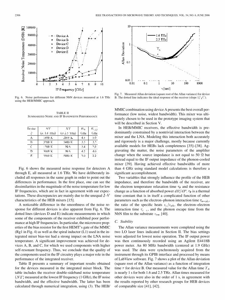
Fig. 6. Noise performance for different NbN devices measured at 1.6 THzusing the HEB/MMIC approach.
TABLE IISUMMARIZED NOISE AND IF BANDWIDTH PERFORMANCE
Fig. 6 shows the measured noise response for detectors Athrough E, all measured at 1.6 THz. We have deliberately in-cluded all responses in the same graph in order to point out thedifferences in performance. In the first place, one can see thedissimilarities in the magnitude of the noise temperature for lowIF frequencies, which are in fact in agreement with our expec-tations. These discrepancies are mainly due to the unequal –characteristics of the HEB mixers [15].
A noticeable difference in the smoothness of the noise re-sponse for different devices is also apparent from Fig. 6. Thedotted lines (devices D and E) indicate measurements in whichsome of the components of the receiver exhibited poor perfor-mance at high IF frequencies. In particular, the microwave prop-erties of the bias resistor for the first HEMT’s gate of the MMIC(Rg1 in Fig. 4) as well as the spiral inductor (L1) used in the in-tegrated mixer bias-tee had a strong impact on the LNA noisetemperature. A significant improvement was achieved for de-vices A, B, and C, for which we used components with higherself-resonant frequency. Thus, we conclude that the quality ofthe components used in the IF circuitry plays a major role in theperformance of the integrated receiver.
Table II presents a summary of important results obtainedfor the devices measured in the integrated mixer block. Thetable includes the receiver double-sideband noise temperature
measured at the lowest IF frequency (1 GHz), the IF noisebandwidth, and the effective bandwidth. The latter has beencalculated through numerical integration, using (3). The HEB/
Fig. 7. Measured Allan deviation (square root of the Allan variance) for deviceB. The dotted line indicates the ideal response of the receiver (slope 1=
p� ).
MMIC combination using device A presents the best overall per-formance (low noise, widest bandwidth). This mixer was ulti-mately chosen to be used in the prototype imaging system thatwill be described in Section V.
In HEB/MMIC receivers, the effective bandwidth is pre-dominantly constrained by a nontrivial interaction between themixer and the LNA. Modeling this interaction both accuratelyand rigorously is a major challenge, mostly because currentlyavailable models for HEBs lack completeness [35]–[38]. Ag-gravating the matter, the noise parameters of the amplifierchange when the source impedance is not equal to 50 butinstead equal to the IF output impedance of the phonon-cooledmixer [39]. Having achieved effective bandwidths of morethan 4 GHz using standard model calculations is therefore asignificant accomplishment.
Two variables that strongly influence the profile of the HEBimpedance, and therefore the bandwidth of the receiver, arethe electron temperature relaxation time and the resistancechange as a function of absorbed power . is a thermaltime constant that is in itself a complicated function of otherparameters such as the electron–phonon interaction time ,the ratio of the specific heats , the electron–electroninteraction time , and the phonon escape time from theNbN film to the substrate [40].
C. Stability
The Allan variance measurements were completed using thetwo LO laser lines indicated in Section II. The bias settingswere adjusted for lowest noise operation. The IF output powerwas then continuously recorded using an Agilent E4418Bpower meter. An 80 MHz bandwidth (centered at 1.9 GHz)was used. The data were synchronously acquired from theinstrument through its GPIB interface and processed by meansof LabView software. Fig. 7 shows a plot of the Allan deviation(square root of the Allan variance) as a function of integrationtime for device B. Our measured value for the Allan timeis nearly 1 s for both 1.6 and 2.5 THz. Allan times measured forother devices were also in the order of 1 s, in agreement withthe results reported by other research groups for HEB devicesof comparable size [41], [42].
RODRIGUEZ-MORALES et al.: DEVELOPMENT OF INTEGRATED HEB/MMIC RECEIVERS FOR NEAR-RANGE TERAHERTZ IMAGING 2307
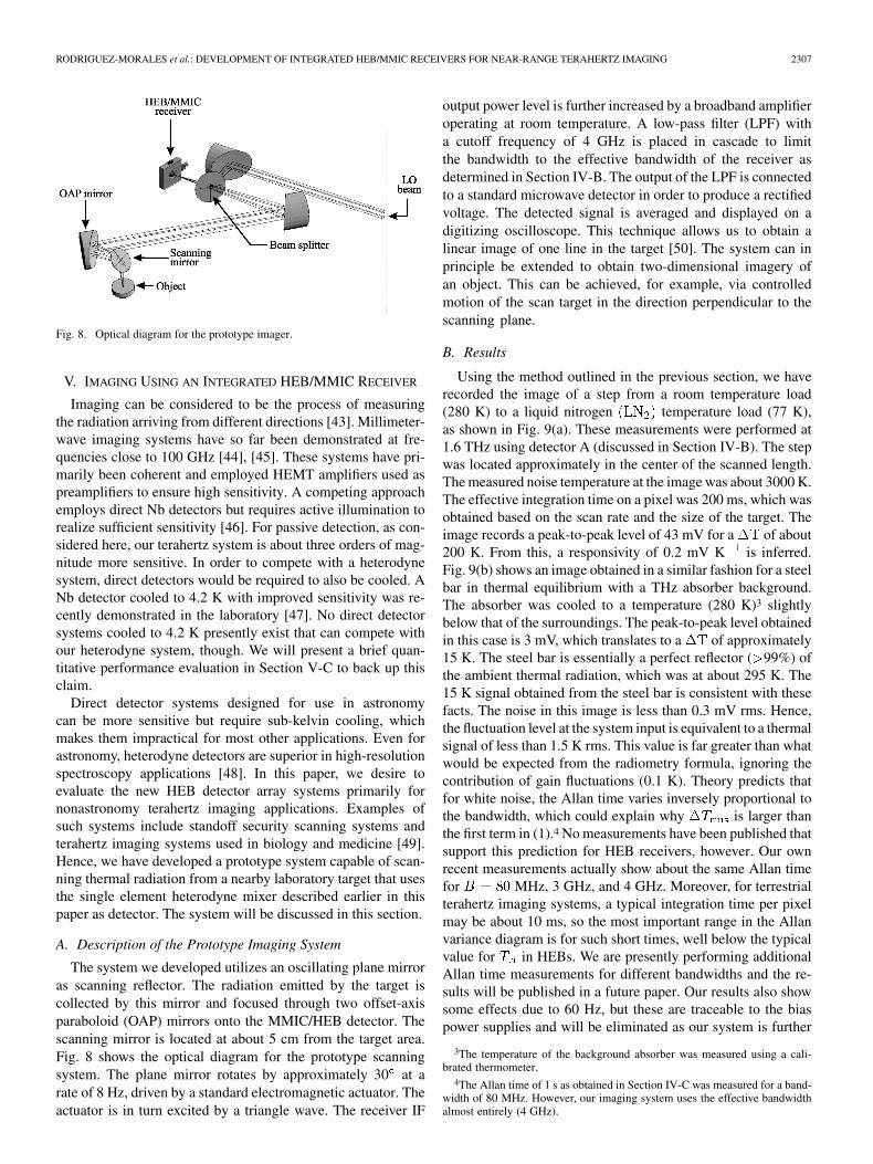
Fig. 8. Optical diagram for the prototype imager.
V. IMAGING USING AN INTEGRATED HEB/MMIC RECEIVER
Imaging can be considered to be the process of measuringthe radiation arriving from different directions [43]. Millimeter-wave imaging systems have so far been demonstrated at fre-quencies close to 100 GHz [44], [45]. These systems have pri-marily been coherent and employed HEMT amplifiers used aspreamplifiers to ensure high sensitivity. A competing approachemploys direct Nb detectors but requires active illumination torealize sufficient sensitivity [46]. For passive detection, as con-sidered here, our terahertz system is about three orders of mag-nitude more sensitive. In order to compete with a heterodynesystem, direct detectors would be required to also be cooled. ANb detector cooled to 4.2 K with improved sensitivity was re-cently demonstrated in the laboratory [47]. No direct detectorsystems cooled to 4.2 K presently exist that can compete withour heterodyne system, though. We will present a brief quan-titative performance evaluation in Section V-C to back up thisclaim.
Direct detector systems designed for use in astronomycan be more sensitive but require sub-kelvin cooling, whichmakes them impractical for most other applications. Even forastronomy, heterodyne detectors are superior in high-resolutionspectroscopy applications [48]. In this paper, we desire toevaluate the new HEB detector array systems primarily fornonastronomy terahertz imaging applications. Examples ofsuch systems include standoff security scanning systems andterahertz imaging systems used in biology and medicine [49].Hence, we have developed a prototype system capable of scan-ning thermal radiation from a nearby laboratory target that usesthe single element heterodyne mixer described earlier in thispaper as detector. The system will be discussed in this section.
A. Description of the Prototype Imaging System
The system we developed utilizes an oscillating plane mirroras scanning reflector. The radiation emitted by the target iscollected by this mirror and focused through two offset-axisparaboloid (OAP) mirrors onto the MMIC/HEB detector. Thescanning mirror is located at about 5 cm from the target area.Fig. 8 shows the optical diagram for the prototype scanningsystem. The plane mirror rotates by approximately 30 at arate of 8 Hz, driven by a standard electromagnetic actuator. Theactuator is in turn excited by a triangle wave. The receiver IF
output power level is further increased by a broadband amplifieroperating at room temperature. A low-pass filter (LPF) witha cutoff frequency of 4 GHz is placed in cascade to limitthe bandwidth to the effective bandwidth of the receiver asdetermined in Section IV-B. The output of the LPF is connectedto a standard microwave detector in order to produce a rectifiedvoltage. The detected signal is averaged and displayed on adigitizing oscilloscope. This technique allows us to obtain alinear image of one line in the target [50]. The system can inprinciple be extended to obtain two-dimensional imagery ofan object. This can be achieved, for example, via controlledmotion of the scan target in the direction perpendicular to thescanning plane.
B. Results
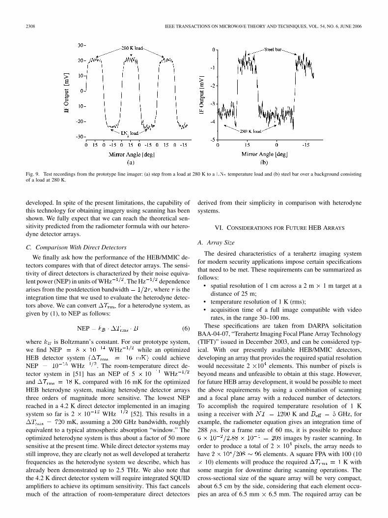
Using the method outlined in the previous section, we haverecorded the image of a step from a room temperature load(280 K) to a liquid nitrogen temperature load (77 K),as shown in Fig. 9(a). These measurements were performed at1.6 THz using detector A (discussed in Section IV-B). The stepwas located approximately in the center of the scanned length.The measured noise temperature at the image was about 3000 K.The effective integration time on a pixel was 200 ms, which wasobtained based on the scan rate and the size of the target. Theimage records a peak-to-peak level of 43 mV for a of about200 K. From this, a responsivity of 0.2 mV K is inferred.Fig. 9(b) shows an image obtained in a similar fashion for a steelbar in thermal equilibrium with a THz absorber background.The absorber was cooled to a temperature (280 K)3 slightlybelow that of the surroundings. The peak-to-peak level obtainedin this case is 3 mV, which translates to a of approximately15 K. The steel bar is essentially a perfect reflector ( 99%) ofthe ambient thermal radiation, which was at about 295 K. The15 K signal obtained from the steel bar is consistent with thesefacts. The noise in this image is less than 0.3 mV rms. Hence,the fluctuation level at the system input is equivalent to a thermalsignal of less than 1.5 K rms. This value is far greater than whatwould be expected from the radiometry formula, ignoring thecontribution of gain fluctuations (0.1 K). Theory predicts thatfor white noise, the Allan time varies inversely proportional tothe bandwidth, which could explain why is larger thanthe first term in (1).4 No measurements have been published thatsupport this prediction for HEB receivers, however. Our ownrecent measurements actually show about the same Allan timefor MHz, 3 GHz, and 4 GHz. Moreover, for terrestrialterahertz imaging systems, a typical integration time per pixelmay be about 10 ms, so the most important range in the Allanvariance diagram is for such short times, well below the typicalvalue for in HEBs. We are presently performing additionalAllan time measurements for different bandwidths and the re-sults will be published in a future paper. Our results also showsome effects due to 60 Hz, but these are traceable to the biaspower supplies and will be eliminated as our system is further
3The temperature of the background absorber was measured using a cali-brated thermometer.
4The Allan time of 1 s as obtained in Section IV-C was measured for a band-width of 80 MHz. However, our imaging system uses the effective bandwidthalmost entirely (4 GHz).
2308 IEEE TRANSACTIONS ON MICROWAVE THEORY AND TECHNIQUES, VOL. 54, NO. 6, JUNE 2006
Fig. 9. Test recordings from the prototype line imager: (a) step from a load at 280 K to a LN temperature load and (b) steel bar over a background consistingof a load at 280 K.
developed. In spite of the present limitations, the capability ofthis technology for obtaining imagery using scanning has beenshown. We fully expect that we can reach the theoretical sen-sitivity predicted from the radiometer formula with our hetero-dyne detector arrays.
C. Comparison With Direct Detectors
We finally ask how the performance of the HEB/MMIC de-tectors compares with that of direct detector arrays. The sensi-tivity of direct detectors is characterized by their noise equiva-lent power (NEP) in units of WHz . The Hz dependencearises from the postdetection bandwidth , where is theintegration time that we used to evaluate the heterodyne detec-tors above. We can convert for a heterodyne system, asgiven by (1), to NEP as follows:
NEP (6)
where is Boltzmann’s constant. For our prototype system,we find NEP WHz while an optimizedHEB detector system could achieveNEP WHz . The room-temperature direct de-tector system in [51] has an NEP of 5 10 WHzand K, compared with 16 mK for the optimizedHEB heterodyne system, making heterodyne detector arraysthree orders of magnitude more sensitive. The lowest NEPreached in a 4.2 K direct detector implemented in an imagingsystem so far is 2 10 WHz [52]. This results in a
mK, assuming a 200 GHz bandwidth, roughlyequivalent to a typical atmospheric absorption “window.” Theoptimized heterodyne system is thus about a factor of 50 moresensitive at the present time. While direct detector systems maystill improve, they are clearly not as well developed at terahertzfrequencies as the heterodyne system we describe, which hasalready been demonstrated up to 2.5 THz. We also note thatthe 4.2 K direct detector system will require integrated SQUIDamplifiers to achieve its optimum sensitivity. This fact cancelsmuch of the attraction of room-temperature direct detectors
derived from their simplicity in comparison with heterodynesystems.
VI. CONSIDERATIONS FOR FUTURE HEB ARRAYS
A. Array Size
The desired characteristics of a terahertz imaging systemfor modern security applications impose certain specificationsthat need to be met. These requirements can be summarized asfollows:
• spatial resolution of 1 cm across a 2 m 1 m target at adistance of 25 m;
• temperature resolution of 1 K (rms);• acquisition time of a full image compatible with video
rates, in the range 30–100 ms.These specifications are taken from DARPA solicitation
BAA-04-07, “Terahertz Imaging Focal Plane Array Technology(TIFT)” issued in December 2003, and can be considered typ-ical. With our presently available HEB/MMIC detectors,developing an array that provides the required spatial resolutionwould necessitate 2 10 elements. This number of pixels isbeyond means and unfeasible to obtain at this stage. However,for future HEB array development, it would be possible to meetthe above requirements by using a combination of scanningand a focal plane array with a reduced number of detectors.To accomplish the required temperature resolution of 1 Kusing a receiver with K and GHz, forexample, the radiometer equation gives an integration time of288 s. For a frame rate of 60 ms, it is possible to produce
images by raster scanning. Inorder to produce a total of 2 10 pixels, the array needs tohave elements. A square FPA with 100 (10
10) elements will produce the required K withsome margin for downtime during scanning operations. Thecross-sectional size of the square array will be very compact,about 6.5 cm by the side, considering that each element occu-pies an area of 6.5 mm 6.5 mm. The required array can be

RODRIGUEZ-MORALES et al.: DEVELOPMENT OF INTEGRATED HEB/MMIC RECEIVERS FOR NEAR-RANGE TERAHERTZ IMAGING 2309
reduced to a smaller size linear configuration with scanning ifthe total target area is decreased and/or the special resolution (orframe time) requirements are relaxed. For security applications,a better tradoff between small array size and sufficiently small
is expected for frequencies slightly lower than 1 THz,considering that the attenuation of typical clothing materials islower in that region of the spectrum [53].
B. Cooling and Field Operation
At the moment, terahertz HEB receivers are all operated incryogenic dewars that must be refilled with liquid helium aboutonce every 24 h (see, for example, [9]). This is appropriate forastronomical receivers, but HEB receiver systems for other ap-plications need to be integrated in a closed-cycle refrigeratorsystem. There are refrigerator systems available for laboratoryuse from several companies. These are still bulky and requirelarge amounts of electrical power and often cooling water forthe compressor unit, but could be used in medical/biologicalimaging applications, for example. A portable terahertz cameracan potentially be developed based on cooling systems under de-velopment for space applications [54], [55]. Such coolers wouldneed extensive (and expensive) further development in order tominimize power consumption, size, and weight for a portableapplication. Nonetheless, they could be realized if a sufficientlyattractive application arises.
VII. CONCLUSION
A new type of integrated receiver for terahertz frequenciesbased on NbN HEB mixers and InP MMIC IF amplifiers hasbeen presented and extensively characterized. Measurementresults are reported for 1.6 and 2.5 THz over a very broadbandIF frequency range. The noise performance of the integratedreceivers is in the range of 10–20 . Effective receiverbandwidths up to 5 GHz can be achieved using this technology.The integrated quasi-optical detectors provide an importantadvantage for multiple receiver systems such as focal planearrays. In fact, a prototype FPA that makes use of this type ofintegrated detectors has been previously demonstrated [15].We have also presented a prototype imaging system that uti-lizes an HEB/MMIC receiver. At this stage, the features ofthe imaging system are limited. However, the capability forproducing images through scanning has been demonstrated.The imaging system is undergoing several improvements whilea more complete system, also based on HEB/MMIC detectors,is being built. It is expected that presently available solid-stateLO sources will help further reduce the overall system size.Potential uses for the HEB/MMIC receivers range from astro-physics to medical diagnostics and surveillance.
ACKNOWLEDGMENT
Grateful acknowledgement is made to Dr. S. Weinreb, JetPropulsion Laboratory, Pasadena, CA, for supplying the MMICchips as well as Dr. P. Khosropanah, Chalmers University ofTechnology, Göteborg, Sweden, for device fabrication. The au-thors are also grateful to V. Fath, University of Massachusettsat Amherst, for his help on the receiver block assembly.
REFERENCES
[1] P. H. Siegel, “Terahertz technology,” IEEE Trans. Microw. TheoryTech., vol. 50, no. 3, pp. 910–928, Mar. 2002.
[2] T. Mimura, “The early history of the high electron mobility transistor(HEMT),” IEEE Trans. Microw. Theory Tech., vol. 50, no. 3, pp.780–782, Mar. 2002.
[3] M. Pospieszalski and E. Wollack, “Ultra-low-noise, InP field effecttransistor radio astronomy receivers: State-of-the-art,” in Proc. 13th Int.Conf. Microw.s, Radar Wireless Commun (MIKON-2000), May 2000,vol. 3, pp. 23–32.
[4] N. Wadefalk, A. Mellberg, I. Angelov, M. Barsky, S. Bui, E. Choumas,R. Grundbacher, E. Kollberg, R. Lai, N. Rorsman, P. Starski, J. Ste-narson, D. Streit, and H. Zirath, “Cryogenic wide-band ultra-low-noiseIF amplifiers operating at ultra-low dc power,” IEEE Trans. Microw.Theory Tech., vol. 50, no. 6, pp. 1705–1711, Jun. 2003.
[5] A. Tessmann, “220-GHz metamorphic HEMT amplifier MMICs forhigh-resolution imaging applications,” IEEE J. Solid-State Circuits,vol. 40, no. 10, pp. 2070–2076, Oct. 2005.
[6] S. Weinreb, R. Lai, N. Erickson, T. Gaier, and J. Wielgus, “W-band InPwideband MMIC LNA with 30 K noise temperature,” in IEEE MTT-SInt. Microw. Symp. Dig., 1999, vol. 1, pp. 101–104.
[7] J. Hacker, J. Bergman, G. Nagy, G. Sullivan, C. Kadow, H. Lin, A.Gossard, M. Rodwell, and B. Brar, “An ultra-low power InAs/AlSbHEMT Ka-band low-noise amplifier,” IEEE Microw. Compon. Lett.,vol. 14, no. 4, pp. 156–158, Apr. 2004.
[8] D. Dawson, L. Samoska, A. Fung, K. Lee, R. L. R. G. P. Liu, andR. Raja, “Beyond G-band: A 235 GHz InP MMIC amplifier,” IEEEMicrow. Compon. Lett., vol. 15, no. 12, pp. 874–876, Dec. 2005.
[9] E. Gerecht, S. Yngvesson, J. Nicholson, Y. Zhuang, F. Rodriguez-Morales, X. Zhao, D. Gu, R. Zannoni, M. Coulombe, J. Dickinson,T. Goyette, W. Gorveatt, J. Waldman, P. Khosropanah, C. Groppi,A. Hedden, D. Golish, C. Walker, J. Kooi, R. Chamberlin, A. Stark,C. Martin, R. Stupak, N. Tothill, and A. Lane, “Deployment ofTREND—A low noise receiver user instrument at 1.25 THz to 1.5THz for AST/RO at the South Pole,” in Proc. 14th Int. Space TerahertzTechnol. Symp., Tucson, AZ, Apr. 2003, pp. 179–188.
[10] S. Cherednichenko, M. Kroug, H. Merkel, P. Khosropanah, A. Adam,E. Kollberg, D. Loudkov, G. Goltsman, B. Voronov, H. Richter, andH.-W. Huebers, “1.6 THz heterodyne receiver for the far infrared spacetelescope,” Phys. C, vol. 372–376, pp. 427–431, 2002.
[11] T. H. Buttgenbach, “An improved solution for integrated array opticsin quasi-optical mm and submm receiver: The hybrid antenna,” IEEETrans. Microw. Theory Tech., vol. 41, no. 10, pp. 1750–1760, Oct.1993.
[12] S. Padin, D. Woody, J. A. Stern, H. LeDuc, R. Blundell, C. Tong, andM. Pospieszalski, “An integrated SIS mixer and HEMT IF amplifier,”IEEE Trans. Microw. Theory Tech., vol. 44, no. 6, pp. 987–990, Jun.1996.
[13] V. P. Koshelets and S. V. Shitov, “Integrated superconducting re-ceivers,” Supercond. Sci. Technol., vol. 13, pp. R53–R69, 2000.
[14] E. Gerecht, C. Musante, Y. Zhuang, K. Yngvesson, T. Goyette, J. Dick-inson, J. Waldman, P. Yagoubov, G. Gol’tsman, B. Voronov, and E.Gershenzon, “NbN hot electron bolometric mixers, a new technologyfor low-noise THz receivers,” IEEE Trans. Microw. Theory Tech., vol.47, no. 12, pp. 2519–2527, Dec. 1999.
[15] F. Rodriguez-Morales, K. S. Yngvesson, E. Gerecht, N. Wadefalk, J.Nicholson, D. Gu, X. Zhao, T. Goyette, and J. Waldman, “A terahertzfocal plane array using HEB superconducting mixers and MMIC IFamplifiers,” IEEE Microw. Compon. Lett., vol. 15, no. 4, pp. 199–201,Apr. 2005.
[16] F. Rodriguez-Morales and K. Yngvesson, “Integrated THz receiversbased on NbN HEB mixers and InP MMIC IF amplifiers,” in IEEEMTT-S Int. Microw. Symp. Dig., 2005, pp. 435–438.
[17] R. Dengler, A. Skalare, and P. Siegel, “Passive and active imaging ofhumans for contraband detection at 640 GHz,” in IEEE MTT-S Int.Microw. Symp. Dig., Jun. 2004, vol. 3, pp. 1591–1594.
[18] S. Weinreb and N. Wadefalk, 2005, private communication.[19] N. Wadefalk and S. Weinreb, “Very low noise amplifiers for very large
arrays,” presented at the IEEE MTT-S Int. Microw. Symp./Very LargeMicrow. Arrays Radio Astron. Space Commun. Workshop, LongBeach, CA, Jun. 2005.
[20] D. DeBoer and D.-J. Bock, “The Allen telescope array: Splitting theaperture,” IEEE Micro, vol. 5, pp. 46–53, Jun. 2004.
[21] F. Rodriguez-Morales and K. Yngvesson, “Impedance and bandwidthcharacterization of NbN hot electron bolometric mixers,” in Proc. 14thInt. Symp. Space Terahertz Tech., Tucson, AZ, Apr. 2003, pp. 431–438.
2310 IEEE TRANSACTIONS ON MICROWAVE THEORY AND TECHNIQUES, VOL. 54, NO. 6, JUNE 2006
[22] A. Maestrini, J. Ward, H. Javadi, E. Schlecht, G. Chattopadhyay, F.Maiwald, N. Erickson, and I. Mehdi, “A 1.7–1.9 THz local oscillatorsource,” IEEE Microw. Compon. Lett., vol. 14, no. 6, pp. 253–255, Jun.2004.
[23] J. Hesler, D. Porterfield, W. Bishop, T. Crowe, A. Baryshev, R. Hesper,and J. Baselmans, “Development and characterization of an easy-to-useTHz source,” in Proc. 16th Int. Space Terahertz Technol. Symp., Göte-borg, Sweden, May 2005, pp. 378–381.
[24] A. Maestrini, J. Ward, H. Javadi, C. Tripon-Canseliet, J. Gill, G. Chat-topadhyay, E. Schlecht, and I. Mehdi, “Local oscillator chain for 1.55to 1.75 THz with 100-�W peak power,” IEEE Microw. Compon. Lett.,vol. 15, no. 12, pp. 871–873, Dec. 2005.
[25] C. Balanis, Antenna Theory: Analysis and Design. New York: Wiley,1997.
[26] D. F. Filipovic, S. S. Gearhart, and G. M. Rebeiz, “Double-slotantennas on extended hemispherical and elliptical silicon dielectriclenses,” IEEE Trans. Microw. Theory Tech., vol. 41, no. 10, pp.1738–1749, Oct. 1993.
[27] J. D. Krauss, Radio Astronomy. Powell, OH: Cygnus-Quasar Books,1986.
[28] F. T. Ulaby, R. K. Moore, and A. K. Fung, Microwave Remote Sensing:Active and Passive, Vol. I—Microwave Remote Sensing Fundamentalsand Radiometry. Reading, MA: Addison-Wesley, 1981.
[29] T. de Graauw, E. Caux, R. Gusten, W. Jellema, W. Luinge, J. Pearson,T. Phillips, R. Schieder, J. Stutzki, K. Wafelbakker, N. Whybom, and K.Wildeman, “The Herschel-Heterodyne Instrument for the far-infrared(HIFI),” in Proc. Joint 29th Int. Conf. IR MM Waves 12th Int. Conf.Terahertz Electron., 2004, pp. 579–580.
[30] J. Kooi, G. Chattopadhyay, M. Thielman, T. Phillips, and R. Schieder,“Noise stability of SIS receivers,” Int. J. Infrared Millim. Waves, vol.21, no. 5, pp. 698–716, May 2000.
[31] D. Allan, “Should the classical variance be used as a basic measure instandards metrology?,” IEEE Trans. Instrum. Meas., vol. IM-36, no. 3,pp. 646–654, Jun. 1987.
[32] J. Kooi, J. Baselmans, A. Baryshev, R. S. M. Hajenius, J. Gao, T. Klap-wijk, B. Voronov, and G. Gol’tsman, “Stability of heterodyne terahertzreceivers,” J. Appl. Phys., 2005, submitted for publication.
[33] M. Ji, “Lens coupled printed antenna characterization,” M.S. thesis,Univ. Massachusetts at Amherst, Amherst, MA, 2001.
[34] X. Zhao, “Integrated antennas for THz hot electron bolometer mixers,”M.S. thesis, Univ. Massachusetts at Amherst, Amherst, MA, 2005.
[35] H. Ekstroem, B. Karasik, E. Kollberg, and K. Yngvesson, “Conversiongain and noise of niobium superconducting hot-electron mixers,” IEEETrans. Microw. Theory Tech., vol. 43, no. 4, pp. 938–947, Apr. 1995.
[36] M. Kroug, “NbN hot electron bolometer mixers for a quasi-opticalTHz receiver,” Ph.D. dissertation, Chalmers Univ. Technol., Göteborg,Sweden, 2001.
[37] H. Merkel, P. Khosropanah, P. Yagoubov, and E. Kollberg, “A hot-spotmixer model for phonon-cooled NbN hot electron bolometric mixers,”IEEE Trans. Appl. Superconduct., vol. 9, no. 6, pp. 4201–4204, Jun.1999.
[38] H. Merkel, P. Khosropanah, S. Yngvesson, S. Cherednichenko, M.Kroug, A. Adam, and E. Kollberg, “An active zone small signal modelfor hot electron bolometric mixers,” in Proc. 12th Int. Space TerahertzTechnol. Symp., San Diego, CA, Feb. 2001, pp. 67–74.
[39] R. Hu and S. Weinreb, “A novel wide-band noise parameter measure-ment method and its cryogenic application,” IEEE Trans. Microw.Theory Tech., vol. 52, no. 5, pp. 1498–1507, May 2004.
[40] S. Cherednichenko, M. Kroug, H. Merkel, E. Kollberg, K. Yngvesson,B. Voronov, and G. Gol’tsman, “IF bandwidth of phonon cooledHEB mixers made from NbN films on MgO substrates,” in Proc. 11thInt. Space Terahertz Technol. Symp., Ann Arbor, MI, May 2000, pp.219–227.
[41] T. Berg, S. Cherednichenko, V. Drakinskiy, H. Merkel, E. Kollberg,and J. Kooi, “Stability measurements of NbN HEB receiver at THzfrequencies,” in Proc. 15th Int. Symp. Space Terahertz Technol.,Northampton, MA, Apr. 2004, pp. 25–32.
[42] J. Baselmans, M. Hajenius, J. Gao, A. Baryshev, J. Kooi, T. Klap-wijk, B. Voronov, P. deKorte, and G. Gol’tsman, “NbN hot electronbolometer mixers: Sensitivity, LO power, direct detection and stability,”IEEE Trans. Appl. Superconduct., vol. 15, no. 6, pp. 485–489, Jun.2005.
[43] P. Goldsmith, C.-T. Hsieh, G. Huguenin, J. Kapitzky, and E. Moore,“Focal plane imaging systems for millimeter wavelengths,” IEEETrans. Microw. Theory Tech., vol. 41, no. 10, pp. 1664–1675, Oct.1993.
[44] D. C. W. Lo, L. Yujiri, G. Dow, T. Ton, M. Mussetto, and B. Allen,“AW -band direct-detection radiometric imaging array,” in IEEE 1994Microw. MM-Wave Monolithic Circuits Symp., 1994, pp. 41–44.
[45] L. Yujiri, M. Shoucri, and P. Moffa, “Passive millimeter waveimaging,” IEEE Micro, vol. 4, no. 3, pp. 39–50, Sep. 2003.
[46] E. N. Grossman, A. Luukanen, and A. J. Miller, “Terahertz active directdetection imagers,” in Proc. SPIE , 2004, vol. 5411, pp. 68–77.
[47] A. Luukanen and J. P. Pekola, “A superconducting antenna-coupledhot-spot microbolometer,” Appl. Phys. Lett., vol. 82, pp. 3970–3972,Jun. 2003.
[48] J. Stutzki, U. Graf, C. Honingh, K. Jacobs, R. Schieder, and Siebertz,“Terahertz receivers for astronomy,” in Proc. Joint 30th Int. Conf. IRMM Waves 13th Int. Conf. Terahertz Electron., Sep. 2005, vol. 2, pp.403–404.
[49] P. H. Siegel, “Terahertz technology in biology and medicine,” IEEETrans. Microw. Theory Tech., vol. 52, no. 10, pp. 2438–2447, Oct.2004.
[50] R. Zannoni, S. Yngvesson, F. Rodriguez-Morales, J. Nicholson, D. Gu,and E. Gerecht, “A prototype terrestrial terahertz imaging system,” inProc. 16th Int. Symp. Space Terahertz Tech., Göteborg, Sweden, pp.93–97.
[51] A. Luukanen, A. J. Miller, and E. N. Grossman, “Active mil-limeter-wave video rate imaging with staring 120-element mi-crobolometer array,” Proc. SPIE, vol. 5411, pp. 195–201, 2004.
[52] ——, “Passive hyperspectral terahertz imagery for security screeningusing a cryogenic microbolometer,” Proc. SPIE, vol. 5789, pp.125–134, 2004.
[53] J. E. Bjarnason, T. L. J. Chan, A. W. M. Lee, M. A. Celis, and E. R.Brown, “Millimeter-wave, terahertz, and mid-infrared transmissionthrough common clothing,” Appl. Phys. Lett., vol. 85, no. 4, pp.519–521, Jul. 2004.
[54] D. Glaister, W. Gully, R. Ross, R. Stack, and E. Marquardt, “Ballaerospace 4–10 K space cryocoolers,” Proc. SPIE, vol. 5498, pp.768–774, Oct. 2004.
[55] R. Ross, Cryocoolers 13. Berlin, Germany: Springer-Verlag, 2005.
Fernando Rodriguez-Morales (S’00) received theB.S. degree in electronics engineering (cum laude)from Universidad Autónoma Metropolitana, México,in 1999, the M.Sc. degree in electrical and computerengineering from the University of Massachusetts atAmherst, in 2003, and is currently working towardthe Ph.D. degree at the University of Massachusettsat Amherst.
From 2000 to 2001, he was with the Department ofPhysics and Astronomy, University of Massachusettsat Amherst, where he collaborated in the develop-
ment of single electron transistor devices as well as semiconductor bolometerarrays. His research interests include the development of highly integratedHEB focal plane arrays for terahertz frequencies, as well as microwave andmillimeter-wave circuit design and characterization.
K. Sigfrid Yngvesson (M’62–SM’92–F’98–LF’02)was born in Lidkoping, Sweden, in 1936. He receivedthe Civilingenjor, Tekn.Lic., and Tekn.Dr. degrees inelectrical engineering from Chalmers University ofTechnology, Göteborg, Sweden, in 1958, 1965, and1968, respectively.
He was a Postdoctoral Fellow with the Departmentof Physics, University of California, Berkeley, in the1960s. He has been with the Department of Electricaland Computer Engineering, University of Massachu-setts at Amherst, since 1970, where he became a full
Professor in 1978. He has worked on quantum electronic low-noise receivers forradio astronomy and on integrated arrays of antenna elements and active deviceswith applications to imaging and power combining. His present main researchinterests are in the areas of quasi-optical terahertz low-noise devices and appli-cations. He is the author of Microwave Semiconductor Devices (Kluwer, 1991).
RODRIGUEZ-MORALES et al.: DEVELOPMENT OF INTEGRATED HEB/MMIC RECEIVERS FOR NEAR-RANGE TERAHERTZ IMAGING 2311
Richard Zannoni received the B.S. degree in elec-trical engineering and mathematics from the Univer-sity of Massachusetts at Amherst, in 2004, where heis currently working toward the M.S. degree in elec-trical engineering.
His current research focuses on improving hotelectron bolometer systems for high-speed imaging.
Eyal Gerecht (S’88–M’97) received the B.S.E.E.degree in electrical engineering with a minor insolid-state physics (magna cum laude) from theUniversity of Houston, Houston, TX, in 1990, andthe M.S.E.C.E. and Ph.D. degrees in electrical andcomputer engineering from the University of Massa-chusetts at Amherst, in 1994 and 1998, respectively.
In 1998, he joined the Department of Physics andAstronomy, University of Massachusetts at Amherst,as a Senior Postdoctoral Research Associate. Since2000, he has been a Physicist with the Electromag-
netic Division, National Institute of Standards and Technology, Boulder, CO,developing a number of terahertz-related technologies. His interests also includethe development of receivers for millimeter and submillimeter applications.
Dr. Gerecht is a member of Tau Beta Pi and Eta Kappa Nu.
Dazhen Gu (S’01) received the B.S. degree inphysics from Nanjing University, Nanjing, China, in1999 and the M.S. degree in electrical engineeringfrom the University of Massachusetts at Amherst,in 2004, where he is currently working toward thePh.D. degree in electrical engineering.
From 1999 to 2001, he was a Research Assistantwith the Superconductor Electronics Laboratory,Nanjing University, where he worked on thethree-terminal device employing high Tc supercon-ductor, ferroelectric, and ferromagnetic materials.
Since 2001, he has been involved in the design and fabrication of NbN hotelectron bolometric mixers for terahertz receivers. Since November 2003, hehas been with the Electromagnetics Division, National Institute of Standardsand Technology, Boulder, CO, where he is engaged in the development ofterahertz imaging systems and characterization of low-noise amplifiers. Hisresearch interest includes nanofabrication, quantum electronics, and RF circuitdesign.
Xin Zhao received the B.S. degree in physics fromthe University of Science and Technology, China, in2000, and the M.S. degree in electrical and computerengineering from the University of Massachusetts atAmherst, in 2005.
From 2002 to 2005, he was a Graduate Re-search Assistant with the Terahertz Laboratory,University of Massachusetts at Amherst, wherehis work focused on antenna design and numericalelectromagnetic analysis and simulations, as wellas measurements in the terahertz frequency range.
Since 2005, he has been with Mathworks Inc, Natick, MA, developing hardwareconnectivity and data analysis software for test and measurement applications.
Niklas Wadefalk was born in Göteborg, Sweden, onMay 14, 1973. He received the B.Sc. degree in elec-trical engineering from the Chalmers University ofTechnology, Göteborg, Sweden, in 1994.
Since 1995, he has been with the MicrowaveElectronics Laboratory Group, Chalmers Universityof Technology, except from 2001 to 2005, whenhe was with the RF and Microwave Group, Cali-fornia Institute of Technology, Pasadena, where hedeveloped cryogenic MMIC amplifiers for variousprojects in the radio astronomy field such as the
Allen Telescope array. His current research interests are broadband MMICLNAs, microwave differential amplifiers, FET characterization, and noise-mea-surement techniques.
John J. Nicholson received the B.S. degree inmarine biology and the associate degree in industrialtechnology/electronics and engineering science fromSoutheastern Massachusetts University of NorthDartmouth (presently University of Massachusettsat Amherst) in 1976, 1984, and 1989, respectively.
From 1987 to 1996, he was with MillitechCorporation working on millimeter-wave andsubmillimeter-wave whisker contacted multipliersbefore becoming a semiconductor process engineer.He continued this work at Millivision, LLC, and
became Lab Manager of the semiconductor fabrication facility. He joined theTREND group as a Research Engineer for the Department of Electrical andComputer Engineering, University of Massachusetts at Amherst, in May 2001,where he is also a Lab Instructor for the semiconductor fabrication course.
Copyright © 2022 FDOKUMEN