Physics-based electron device modelling and computer-aided MMIC design
20
1333 IEEE TRANSACTIONS ON MICROWAVE THEORY AND TECHNIQUES, VOL. 40, NO. 7, JULY 1992 0 Lintarandmlinear trequencydomaln (Ha- Balance) analysis Phy sics-Based Electron Device Modelling and Computer-Aided MMIC Design Circuit Analysis G = WY) Fabio Filicori, Giovanni Ghione, Member, IEEE, and Carlo U. Naldi, Senior Member, IEEE (Invited Paper) Abstract-The paper provides an overview on the state of the art and future trends in physics-based electron device model- ling for the computer-aided design of monolithic microwave IC’s. After a review of the main physics-based approaches to microwave modelling, special emphasis is placed on innovative developments relevant to circuit-oriented device performance assessment, such as efficient physics-based noise and para- metric sensitivity analysis. The use of state-of-the-art physics- based analytical or numerical models for circuit analysis is dis- cussed, with particular attention to the role of intermediate be- havioural models in linking multidimensional device simulators with circuit analysis tools. Finally, the model requirements for yield-driven MMIC design are discussed, with the aim of point- ing out the advantages of physics-based statistical device modelling; the possible use of computationally efficient ap- proaches based on device sensitivity analysis for yield optimi- zation is also considered. I. INTRODUCTION N THE traditional approach to the design of hybrid or I monolithic microwave IC’s (MMIC’s) the circuit is built around packaged or foundry devices which are modelled by behavioral electrical models (e.g., equiva- lent circuits), characterized through standard or on-chip measurements performed on manufactured prototypes. Circuit optimization is performed in the space of the elec- trical or geometrical parameters of the passive elements. Conversely, in the physics-based approach to MMIC de- sign, optimization also involves the technological param- eters of the active devices. This requires that the active devices be characterized through physical models, which provide the link between the physical and process input data and the electrical performances within the framework of an integrated CAD environment (see Fig. 1) whose main steps are: Process modelling, relating the process parameters a (i.e., intrinsic semiconductor characteristics, control pa- rameters for epitaxial or ion-implantation processes, ge- ometry of photolithographic masks.. .) to the correspond- ing physical parameters 0 (e.g., activated doping profile, Manuscript received September 16, 1991; revised March I, 1992. This work was partially supported by EEC in the framework of the ESPRIT 255 and 5018 COSMIC projects. Partial support has also been provided from the Italian National Research Council (CNR). F. Filicori is with the Universita di Ferrara, Istituto di Ingegneria, Via Scandiana 21, 44100 Ferrara, Italy, and with the Centro di Studio fer I’In- terazione Operatore-Calcolatone Facolta di Ingegneria, Viale Risorgi- mento 2, 40136 Bologna, Italy. G. Ghione and C. U. Naldi are with the Dipartimento di Elettronica. Politecnico di Torino, Corso Duca degli Abruzzi 24, Torino. Italy. IEEE Log Number 9200768. a Prooess parameters ’ p Physicaldevice Physics-based 0 Anatytiipmcess models 0 20 numerical models I 0 quasi-20 and 20 Device Modelling numerical and analylii models I I y Electricaldevice Circuit-oriented behavioral 0 Direcl link 0 Intermediate equivalent cirmks 0 Intermedie black-box mathematical models ’TGCi,cuitpebrmance Fig. 1. Functional flow chart for process, device and circuit modelling. actual gate length, recessed gate depth, surface or sub- strate state density.. .) which characterize the manufac- tured semiconductor device. Physics-based device modelling (PBDM), relating the physical parameters 0 to the electrical parameters y (i.e., frequency-dependent S-parameters, dc characteristics, RF transconductance, junction capacitances, noise parame- ters.. .) of a given semiconductor device. Circuit analysis finally providing the link between the electrical device parameters y and the corresponding cir- cuit performance G. There are several reasons for adopting a physics-based approach to MMIC design. In a performance-driven de- sign, PBDMs allow the designer to tailor, at least up to a certain extent, the active devices so as to further improve the circuit response. However, the physics-based ap- proach has special advantages in yield-driven MMIC de- sign, where the electrical device parameters must be char- acterized statistically. In fact, while the physical parameters deriving from the manufacturing process are either practically uncorrelated or subject to simple corre- lations, the statistics of electrical device parameters are affected by complex correlations introduced by the device physics. The cumbersome and expensive characterization of many manufactured device prototypes can be avoided 0018-9480/92$03.00 0 1992 IEEE
Transcript of Physics-based electron device modelling and computer-aided MMIC design
1333 IEEE TRANSACTIONS ON MICROWAVE THEORY AND TECHNIQUES, VOL. 40, NO. 7 , JULY 1992
0 Lintarandmlinear
trequencydomaln (Ha- Balance)
analysis
Phy sics-Based Electron Device Modelling and Computer-Aided MMIC Design
Circuit Analysis G = WY)
Fabio Filicori, Giovanni Ghione, Member, IEEE, and Carlo U. Naldi, Senior Member, IEEE
(Invited Paper)
Abstract-The paper provides an overview on the state of the art and future trends in physics-based electron device model- ling for the computer-aided design of monolithic microwave IC’s. After a review of the main physics-based approaches to microwave modelling, special emphasis is placed on innovative developments relevant to circuit-oriented device performance assessment, such as efficient physics-based noise and para- metric sensitivity analysis. The use of state-of-the-art physics- based analytical or numerical models for circuit analysis is dis- cussed, with particular attention to the role of intermediate be- havioural models in linking multidimensional device simulators with circuit analysis tools. Finally, the model requirements for yield-driven MMIC design are discussed, with the aim of point- ing out the advantages of physics-based statistical device modelling; the possible use of computationally efficient ap- proaches based on device sensitivity analysis for yield optimi- zation is also considered.
I. INTRODUCTION N THE traditional approach to the design of hybrid or I monolithic microwave IC’s (MMIC’s) the circuit is
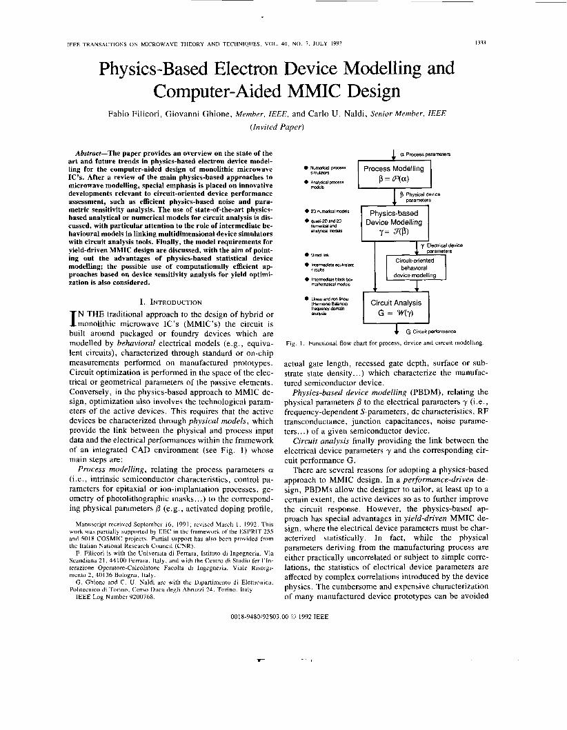
built around packaged or foundry devices which are modelled by behavioral electrical models (e.g., equiva- lent circuits), characterized through standard or on-chip measurements performed on manufactured prototypes. Circuit optimization is performed in the space of the elec- trical or geometrical parameters of the passive elements. Conversely, in the physics-based approach to MMIC de- sign, optimization also involves the technological param- eters of the active devices. This requires that the active devices be characterized through physical models, which provide the link between the physical and process input data and the electrical performances within the framework of an integrated CAD environment (see Fig. 1) whose main steps are:
Process modelling, relating the process parameters a (i.e., intrinsic semiconductor characteristics, control pa- rameters for epitaxial or ion-implantation processes, ge- ometry of photolithographic masks.. .) to the correspond- ing physical parameters 0 (e.g., activated doping profile,
Manuscript received September 16, 1991; revised March I , 1992. This work was partially supported by EEC in the framework of the ESPRIT 255 and 5018 COSMIC projects. Partial support has also been provided from the Italian National Research Council (CNR).
F. Filicori is with the Universita di Ferrara, Istituto di Ingegneria, Via Scandiana 21, 44100 Ferrara, Italy, and with the Centro di Studio fer I’In- terazione Operatore-Calcolatone Facolta di Ingegneria, Viale Risorgi- mento 2, 40136 Bologna, Italy.
G . Ghione and C. U . Naldi are with the Dipartimento di Elettronica. Politecnico di Torino, Corso Duca degli Abruzzi 24, Torino. Italy.
IEEE Log Number 9200768.
a Prooess parameters
’ p Physicaldevice
Physics-based
0 Anatytiipmcess models
0 20 numerical models
I 0 quasi-20 and 20 Device Modelling numerical and analyl i i models
I I y Electrical device
Circuit-oriented behavioral
0 Direcl link
0 Intermediate equivalent cirmks
0 Intermedie black-box mathematical models
’ T G C i , c u i t p e b r m a n c e
Fig. 1. Functional flow chart for process, device and circuit modelling.
actual gate length, recessed gate depth, surface or sub- strate state density.. .) which characterize the manufac- tured semiconductor device.
Physics-based device modelling (PBDM), relating the physical parameters 0 to the electrical parameters y (i.e., frequency-dependent S-parameters, dc characteristics, RF transconductance, junction capacitances, noise parame- ters.. .) of a given semiconductor device.
Circuit analysis finally providing the link between the electrical device parameters y and the corresponding cir- cuit performance G .
There are several reasons for adopting a physics-based approach to MMIC design. In a performance-driven de- sign, PBDMs allow the designer to tailor, at least up to a certain extent, the active devices so as to further improve the circuit response. However, the physics-based ap- proach has special advantages in yield-driven MMIC de- sign, where the electrical device parameters must be char- acterized statistically. In fact, while the physical parameters deriving from the manufacturing process are either practically uncorrelated or subject to simple corre- lations, the statistics of electrical device parameters are affected by complex correlations introduced by the device physics. The cumbersome and expensive characterization of many manufactured device prototypes can be avoided
0018-9480/92$03.00 0 1992 IEEE
1334 IEEE TRANSACTIONS ON MICROWAVE THEORY AND TECHNIQUES, VOL. 40 , NO. 7 . JULY 1992
if the statistics of the electrical parameters is derived, by means of PBDM’s, from the physical parameters whose experimental statistical characterization and Monte Carlo simulation is easier.
In this perspective, the process and device physics- based models menticned above should not only yield the nominal (expected) values for the physical and electrical device parameters, respectively, but also the self and joint probability distributions of the deviations A 0 and Ay be- tween actual and expected values. In the case of small physical parameter changes the electrical parameters can be statistically characterized through the first order ap- proximation Ay = SJ A b , where SJ is the device small- change sensitivity.
The above considerations suggest that PBDMs, tradi- tionally a tool for device design only, should also play an important role in physics-based MMIC design. However, while the computer algorithms for circuit analysis [73], [87], [77], [63], [38], [83], [98] have now reached suffi- cient maturity to enable MMIC optimization even on me- dium-power workstations, the physical device models, on which the accuracy and efficiency of performance predic- tion ultimately depends, still involve considerable com- putational problems.
In fact, a model able to provide complete device per- formance prediction (dc characteristics, bias-dependent small-signal ac parameters, large-signal response, noise, temperature dependence) in terms of physical parameters alone must be based on fundamental semiconductor equa- tions. Unfortunately, even for the relatively simple drift- diffusion model, accurate and general-purpose algorithms for the solution of the PBDM equations require the nu- merical treatment of sets of partial differential equations over a two- or three-dimensional domain. As a conse- quence, numerical physics-based models are computa- tionally intensive and therefore unsuitable for direct in- clusion into CAD tools for circuit analysis and optimization.
The implementation of physical models can be simpli- fied and made more efficient (but possibly less accurate) by taking advantage of the specific structure of microwave FET’s; this leads to the so-called quasi-2D numerical or analytical models. However, although recently proposed numerical quasi-2D models can be used for simple large- signal circuit analyses [88], only analytical models are directly compatible with optimization-driven circuit anal- ysis algorithms based on frequency-domain harmonic- balance (HB) techniques. The use of numerical physics- based device models for circuit analysis, as discussed in Sec. V, is possible only through “off line” device simu- lation and indirect linking with circuit analysis algorithms by means of intermediate behavioral models.
Although the above remarks seem to suggest that only analytical models are really suitable for physics-based MMIC design, this cannot be considered a final conclu- sion in view of the accuracy requirements posed by this task. In fact, success in performing physics-based MMIC
design obviously depends on the accuracy achieved by the physical models used to this aim. However, accuracy re- quirements for PBDM’s are difficult to establish a priori, and should be properly understood. While both fully 2D and simplified models can be highly accurate in reproduc- ing the electrical characteristics of a particular device, as repeatedly shown in the literature, this goal is often achieved by properly adjusting the values of some of the physical input parameters around initial estimates (model tuning). This procedure may ultimately turn the physical model into an almost behavioral model, whose so-called physical input parameters actually depend on the real physical parameters; consequently, the excellent agree- ment shown for a specific device does not guarantee that the physical model is able to accurately reproduce the variations in the electrical characteristics caused by vari- ations in the physical input parameters. Simplified imple- mentations of physical models are expected to suffer from this limitation more than fully 2D numerical implemen- tations.
As discussed in Sec. VI, physics-based performance and above all yield optimization requires a model able not only to accurately simulate the electrical behaviour of a device, but also to closely reproduce the effect of small variations of its physical parameters with respect to the nominal values. This conclusion can be intuitively under- stood when considering that physics-based MMIC opti- mization normally starts from a circuit which has already been performance-optimized around “standard” foundry devices. Now, according to the more or less critical per- formance requirements and to the maturity of the tech- nology, several situations may arise. If the tolerance ranges for circuit performance are not critical, further op- timization is probably useless. The same can be said of yield optimization if the technology is poor; in this case, in fact, the spread in the physical parameters is so large that little can be achieved by design centering, and yield improvement becomes mainly a technological issue. On the other hand, the design of high-performance circuits using a mature technology offers good possibilities in terms both of performance and yield physics-based opti- mization. In either case, however, we expect that, owing to the tight performance tolerances and to the low spread of the physical parameters, performance or yield optimi- zation can be achieved by means of small variations in the physical parameters around the “standard” values of an initial performance-optimized design. This leads to the conclusion that, in order to achieve a practically mean- ingful design, the PBDM must provide a highly accurate estimate of the device sensitivity to physical parameters variations with respect to a nominal condition to which the model has been somehow fitted.
These remarks suggest that physics-based performance or yield optimization, up to now camed out through an- alytical models only, could also take advantage of more complex and potentially more accurate physical models run “off line” with respect to the circuit optimizer, when
FILICORI et al . : PHYSICS-BASED ELECTRON DEVICE MODELLING 1335
these are able to provide a good estimate of the device sensitivity. Such a possibility is offered by the efficient sensitivity analysis techniques presented in Sec. IV. Therefore, while the efforts towards achieving more and more accurate analytical models are certainly worthwhile, the use of the more computationally intensive numerical PBDMs is possible for circuit analysis and yield optimi- zation by the proper use of intermediate behavioural modelling and device sensitivity analysis.
The paper is structured as follows. A comprehensive review of the physics-based modelling of GaAs devices for MMIC’s is presented in Sec. 11, with special emphasis on MESFET’s. Section I11 covers a less conventional topic, i.e., physics-based noise modelling, whose impor- tance both in microwave device design and in physics- based performanc prediction hardly needs to be stressed; some recent developments introduced by the authors in the domain of two-dimensional noise modelling of GaAs FET’s are included. Section IV covers the problem of physics-based device sensitivity analysis and also includes some new material recently developed by the authors. Section V deals with the issue of physics-based circuit analysis carried out either directly through analytical PBDM’s or indirectly through intermediate behavioral models consisting either of large-signal equivalent cir- cuits or of black-box mathematical models, for which some innovative developments are presented. Finally Sec. VI is devoted to a discussion of physics-based MMIC per- formance and yield optimization by means of state-of-the- art analytical PBDMs, and also to some possible devel- opments concerning yield optimization through “off line” multidimensional numerical PBDM’s.
11. PHYSICS-BASED MODELS
A. Process Modelling
Process modelling is an important but critical step in MMIC CAD. In fact, the practical characterization of the GaAS process requires extensive measurements on a spe- cific set of technological facilities; the resulting data can be strongly process-dependent and have limited general validity. An even more demanding task is the statistical characterization of the physical parameters deriving from a given process. For these reasons, efforts toward a com- prehensive GaAs process modelling are comparatively rare; an excellent example is found in the work by Anholt et al. [3], [4], [6]. From the statistical data reported in [6] it can be inferred that improvements in technology have now made the standard deviation of the physical pa- rameters (doping profiles, etch depths, and so on) reason- ably low, i.e., of the order of less that 10% (see Table I1 in [6]). This is important in view of physics-based yield optimization, since whenever the technological uniform- ity is poor, realistic yield improvement is more dependent on progress in technology than on design centering. On the other hand, a good process uniformity and repeatabil-
ity makes yield optimization through design centering meaningful and worth doing.
B. An Overview on the Basic Semiconductor Device Models
Most available physics-based models for GaAs FET’s are based on the drift-diffusion picture of camer trans- port, in which the carrier drift velocity U is a function of the local electric E field through the static field-velocity curve, and the diffusivity D follows the equilibrium Ein- stein relationship. Since the device dimensions are typi- cally much smaller than the operating wavelength, the electric potential and the charge density can be related through Poisson equation. For bipolar transport, the drift- diffusion model reads:
(3)
where n is the electron density, p is the hole density, $J the electric potential, = -V$J the electric field, N i and N A the ionized acceptor and donor densities, R the net recombination rate. The model becomes slightly more complex in heterostructure FETs, since space-dependent bandgaps and semiconductor affinities must be allowed for.
The drift-diffusion model is already a heavy approxi- mation when compared to other, more complete descrip- tions of camer transport. Although quantum effects are globally significant to the operation of many high-fre- quency or optical devices, quantum models (i.e., the Schrodinger equation in the effective mass approxima- tion) can often be applied locally. A typical example is provided by the high electron mobility transistor (HEMT), in which carriers are mostly confined in a quan- tized-system, the so-called two-dimensional electron gas (2DEG). The sheet density of the 2DEG can be separately characterized from a quantum standpoint and the resulting model can be easily interfaced to non-quantum transport models.
Semiclassical transport models deal with camers as classical particles, whose motion properties (effective mass and interactions with lattice impurities, phonons, etc.) derive from quantum models. The fundamental semiclassical model for semiconductor transport is the Boltzmann equation [61] which directly yields the time- and space-dependent momentum distribution function of carriers in the phase space, and therefore provides full information on both low- and high-energy phenomena. The only technique currently able to cope with this model without resorting to drastic approximations is the Mon- tecarlo simulation method [61], [81], which is still too
1336 IEEE TRANSACTIONS ON MICROWAVE THEORY AND TECHNIQUES. VOL. 40, NO. 7. JULY 1992
computationally intensive to enable device design and op- timization, let alone circuit-oriented CAD. From Boltz- mann equation the so-called hydrodynamic transport models can be derived, whose unknowns are the central moments of the carrier distribution, which correspond to the average parameters (average density, average energy, average momentum, and so forth) of the carriers, consid- ered collectively as a carrier gas. Hydrodynamic models are sets of partial differential equations which express, in divergence form, the conservation of the central moments of the carrier distributions [18], [55]; in the case of uni- polar transport, a widely accepted choice leads to a set of three equations for each equivalent minimum of the con- duction band, corresponding to a particle continuity equa- tion (the current continuity equation), an energy transport equation, and a (vector) momentum transport equation.
Several simplifications have been proposed to reduce the computational complexity of the full hydrodynamic model. Firstly, by approximately averaging the transport equations of all the equivalent minima, the single electron gas transport model is obtained [ 181, which has been re- cently exploited for multidimensional device simulation [37]. However, further approximation are often intro- duced, mainly to avoid the explicit solution of the mo- mentum transport equation. By neglecting space and time variations in the momentum equation one obtains the so- called energy transport models (see e .g . , [108]), which can be further simplified by neglecting the kinetic vs. the thermal electron energy of the carriers (temperature models, see e.g., [29]), or the electron heat flow in the energy transport equation [ 1081. Although the above ap- proximations are meant to trade off accuracy for compu- tational efficiency, the errors introduced thereby are dif- ficult to control and the simplified hydrodynamic models yield results which may be as different from each other as from the drift-diffusion model [37]. Drift-diffusion models can be finally considered as hydrodynamic models in which both the energy and the momentum equation are approximated with their steady-state, space-independent expressions. For a more detailed discussion the reader can refer e.g., to [84].
The numerical treatment of hydrodynamic or drift-dif- fusion device models requires discretization and solution algorithms [103, 801. Discretization can be carried out through finite-differences or finite-elements techniques by means of special schemes, like the so-called Scharfetter- Gummel scheme [ 1021. After discretization, the time-do- main physical model becomes a large, sparse system of coupled ordinary non-linear differential equations whose unknowns are, for instance, the charge density, average energy and electric potential at the discretization nodes. The solution step requires this system to be analyzed in the several possible operating conditions of the device. In the dc problem all time derivatives are set to zero and the resulting nonlinear system is solved through Newton linearization; in the ac small-signal problem, device anal- ysis is better carried out in the frequency domain, by means of numerical techniques analogous to those usually
adopted for small-signal circuit analysis. Finally, the large-signal analysis with periodic or arbitrary (transient) excitation, requires the differential system to be solved through time-stepping algorithms, since harmonic-bal- ance analysis in the framework of numerical device sim- ulation would be too computationally intensive. Thus, large-signal multidimensional models have been mainly exploited for transient simulation. For the purpose of complete performance prediction, other less conventional kinds of device analysis should also be considered, like noise and parametric sensitivity analysis. These will be separately discussed in Section I11 and IV, respectively.
C. Quasi-Two Dimensional and Analytical Physics- Based Models
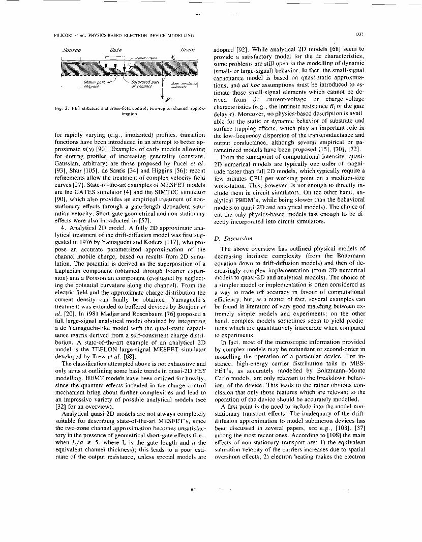
Owing to their computational intensity, exact, multi- dimensional implementations of transport models cannot be directly included into circuit analysis and optimization algorithms; however, proper approximations enable greater computational efficiency in the analysis of specific devices. In particular, the cross-field structure of micro- wave FET’s, in which the channel current and the gate control mechanism are orthogonal (see Fig. 2), suggests an approximate spatial decoupling which is exploited in the so-called quasi-2D implementations of transport models. In most quasi-2D models the gate charge control is treated according to a 1D quasi-equilibrium approxi- mation along y , while the analysis of channel current is reduced to a 1D continuity equation along x. The solution of the two decoupled 1D models can either be numerical or analytical; in its simplest form, the gate control model is based on the depletion approximation and the channel model is based on a two-zone (ohmic and velocity-satu- rated) channel approximation (Fig. 2), which ultimately reduces, for constant mobility, to Shockley’s JFET model. According to the different possible levels of approxima- tion made, several classes of models have been derived, with widely different complexity and accuracy. Repre- sentative examples are:
1. Quasi-2D energy-transport models [25], [ 1091, [88], based on an approximate 1D version of the energy and momentum transport equations; the charge control mech- anism is either analytical or implicit. The computational intensity is not negligible, since the 1D solution for the transport model is performed numerically.
2. Quasi-2D models with numerical charge control and two-zone channel approximation [ 1011, [91]. Such models use an accurate quasi-equilibrium numerical model for charge control [ 1011, [91], which can provide detailed in- sight into the static behavior of substrate impurities and traps. Since the charge control model can be separately solved and the results stored as a look-up table, the com- putational burden is limited.
3 . Quasi-2D models with analytical charge control and two-zone channel model. Since charge control is based on the abrupt depletion approximation (n = 0 under the gate and n = No ( y ) in the conducting channel), which is poor
FILICORI et al . : PHYSICS-BASED ELECTRON DEVICE MODELLING 1337
Source Ca te Drab adopted [92]. While analytical 2D models [68] seem to
Fig. 2 . FET structure and cross-field control; two-region channel approx- imation.
for rapidly varying (e.g., implanted) profiles, transition functions have been introduced in an attempt to better ap- proximate n(y ) [90]. Examples of early models allowing for doping profiles of increasing generality (constant, Gaussian, arbitrary) are those proposed by Puce1 et al. [93], Shur [105]. de Santis [34] and Higgins [56]; recent refinements allow the treatment of complex velocity-field curves [27]. State-of-the-art examples of MESFET models are the GATES simulator [4] and the SIMTEC simulator [90], which also provides an empirical treatment of non- stationary effects through a gate-length dependent satu- ration velocity. Short-gate geometrical and non-stationary effects were also introducted in [57].
4. Analytical 2D model. A fully 2D approximate ana- lytical treatment of the drift-diffusion model was first sug- gested in 1976 by Yamaguchi and Kodera [ 1171, who pro- pose an accurate parametrized approximation of the channel mobile charge, based on results from 2D simu- lation. The potential is derived as the superposition of a Laplacian component (obtained through Fourier expan- sion) and a Poissonian component (evaluated by neglect- ing the potential curvature along the channel). From the electric field and the approximate charge distribution the current density can finally be obtained. Yamaguchi's treatment was extended to buffered devices by Bonjour et al. [20]. In 1981 Madjar and Rosenbaum [76] proposed a full large-signal analytical model obtained by integrating a dc Yamaguchi-like model with the quasi-static capaci- tance matrix derived from a self-consistent charge distri- bution. A state-of-the-art example of an analytical 2D model is the TEFLON large-signal MESFET simulator developed by Trew et al. [68].
The classification attempted above is not exhaustive and only aims at outlining some basic trends in quasi-2D FET modelling. HEMT models have been omitted for brevity, since the quantum effects included in the charge control mechanism bring about further complexities and lead to an impressive variety of possible analytical models (see [32] for an overview).
Analytical quasi-2D models are not always completely suitable for describing state-of-the-art MESFET's, since the two-zone channel approximation becomes unsatisfac- tory in the presence of geometrical short-gate effects (i.e., when L / u Z 5 , where L is the gate length and a the equivalent channel thickness); this leads to a poor esti- mate of the output resistance, unless special models are
provide a satisfactory model for the dc characteristics, some problems are still open in the modelling of dynamic (small- or large-signal) behavior. In fact, the small-signal capacitance model is based on quasi-static approxima- tions, and ad hoc assumptions must be introduced to es- timate those small-signal elements which cannot be de- rived from dc current-voltage or charge-voltage characteristics (e.g., the intrinsic resistance R, or the gate delay 7). Moreover, no physics-based description is avail- able for the static or dynamic behavior of substrate and surface trapping effects, which play an important role in the low-frequency dispersion of the transconductance and output conductance, although several empirical or pa- rametrized models have been proposed [ 151, [70], [72].
From the standpoint of computational intensity, quasi- 2D numerical models are typically one order of magni- tude faster than full 2D models, which typically require a few minutes CPU per working point on a medium-size workstation. This, however, is not enough to directly in- clude them in circuit simulators. On the other hand, an- alytical PBDM's, while being slower than the behavioral models to quasi-2D and analytical models). The choice of ent the only physics-based models fast enough to be di- rectly incorporated into circuit simulators.
D. Discussion
The above overview has outlined physical models of decreasing intrinsic complexity (from the Boltzmann equation down to drift-diffusion models) and then of de- creasingly complex implementation (from 2D numerical models to quasi-2D and analytical models). The choice of a simpler model or implementation is often considered as a way to trade off accuracy in favour of computational efficiency, but, as a matter of fact, several examples can be found in literature of very good matching between ex- tremely simple models and experiments; on the other hand, complex models sometimes seem to yield predic- tions which are quantitatively inaccurate when compared to experiments.
In fact, most of the microscopic information provided by complex models may be redundant or second-order in modelling the operation of a particular device. For in- stance, high-energy carrier distribution tails in MES- FET's, as accurately modelled by Boltzmann-Monte Carlo models, are only relevant to the breakdown behav- iour of the device. This leads to the rather obvious con- clusion that only those features which are relevant to the operation of the device should be accurately modelled.
A first point is the need to include into the model non- stationary transport effects. The inadequacy of the drift- diffusion approximation to model submicron devices has been discussed in several papers, see e .g . , [108], [37] among the most recent ones. According to [ 1081 the main effects of non-stationary transport are: 1) the equivalent saturation velocity of the carriers increases due to spatial overshoot effects; 2) electron heating makes the electron
1338 IEEE TRANSACTIONS ON MICROWAVE THEORY AND TECHNIQUES, VOL. 40, NO. 7, JULY 1992
diffusivity increase, which in turn leads to a widening of the conducting channel; 3) transient response is faster be- cause of time overshoot effects. From the standpoint of microwave operation, transient effects are probably neg- ligible, since time overshoot takes place on a picosecond scale. Conversely, spatial overshoot and carrier heating lead to a higher saturation current ZDss and a higher trans- conductance g,, while the internal device capacitances are not significantly affected (see e.g., [29]). Unfortunately, little agreement is to be found in the literature on the quantitative amount of the increase in IDSS for decreasing gate length in the submicron range.
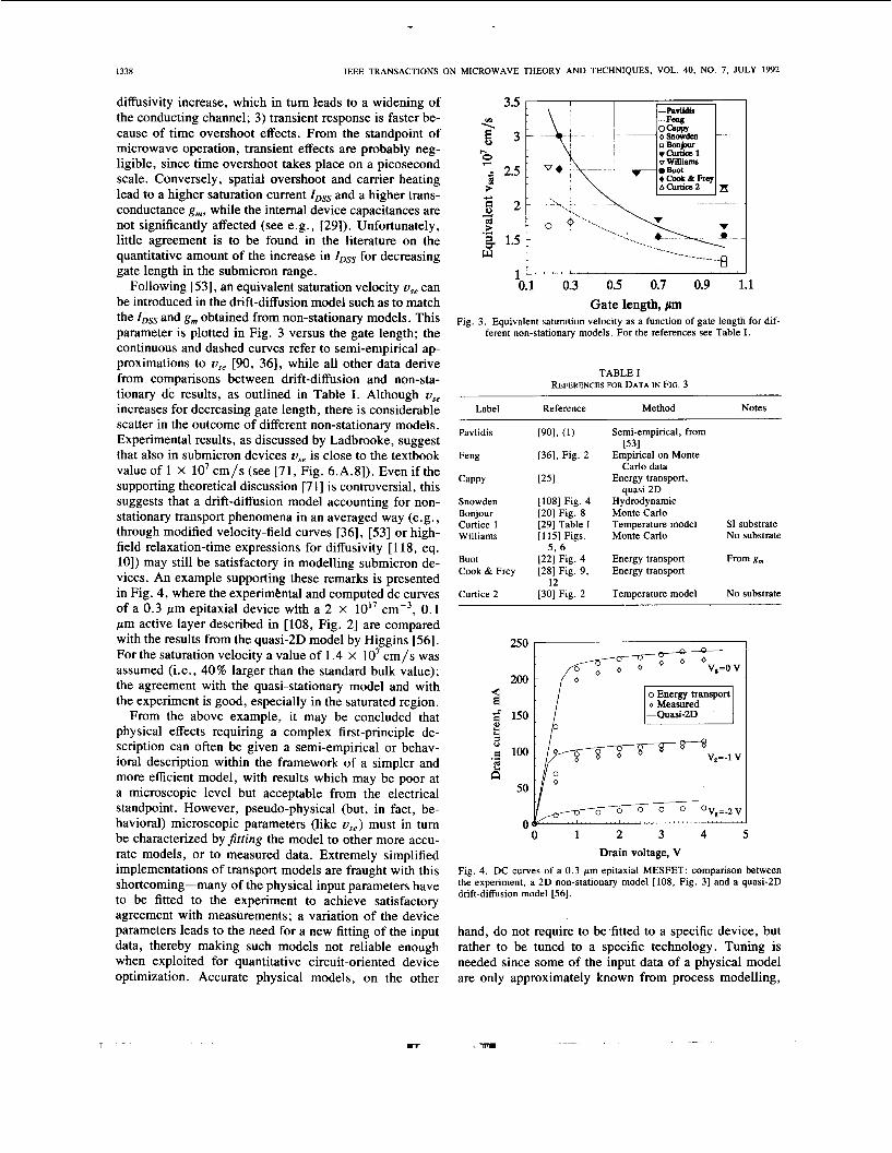
Following [53], an equivalent saturation velocity U,, can be introduced in the drift-diffusion model such as to match the IDSS and g, obtained from non-stationary models. This parameter is plotted in Fig. 3 versus the gate length; the continuous and dashed curves refer to semi-empirical ap- proximations to U,, [90, 361, while all other data derive from comparisons between drift-diffusion and non-sta- tionary dc results, as outlined in Table I. Although U,, increases for decreasing gate length, there is considerable scatter in the outcome of different non-stationary models. Experimental results, as discussed by Ladbrooke, suggest that also in submicron devices U,, is close to the textbook value of 1 X lo7 cm/s (see [71, Fig. 6.A.81). Even if the supporting theoretical discussion [7 13 is controversial, this suggests that a drift-diffusion model accounting for non- stationary transport phenomena in an averaged way (e.g., through modified velocity-field curves [36], [53] or high- field relaxation-time expressions for diffusivity [ 118, eq. lo]) may still be satisfactory in modelling submicron de- vices. An example supporting these remarks is presented in Fig. 4, where the experimkntal and computed dc curves of a 0.3 pm epitaxial device with a 2 x l O I 7 ~ m - ~ , 0 .1 pm active layer described in [108, Fig. 21 are compared with the results from the quasi-2D model by Higgins [56]. For the saturation velocity a value of 1.4 x lo7 cm/s was assumed (i.e., 40% larger than the standard bulk value); the agreement with the quasi-stationary model and with the experiment is good, especially in the saturated region.
From the above example, it may be concluded that physical effects requiring a complex first-principle de- scription can often be given a semi-empirical or behav- ioral description within the framework of a simpler and more efficient model, with results which may be poor at a microscopic level but acceptable from the electrical standpoint. However, pseudo-physical (but, in fact, be- havioral) microscopic parameters (like use) must in turn be characterized by jilting the model to other more accu- rate models, or to measured data. Extremely simplified implementations of transport models are fraught with this shortcoming-many of the physical input parameters have to be fitted to the experiment to achieve satisfactory agreement with measurements; a variation of the device parameters leads to the need for a new fitting of the input data, thereby making such models not reliable enough when exploited for quantitative circuit-oriented device optimization. Accurate physical models, on the other
3.5
3
2.5
2
1.5
1
r \ I-
0.1 0.3 0.5 0.7 0.9 1.1 Gate length, pm
Fig. 3. Equivalent saturation velocity as a function of gate length for dif- ferent non-stationary models. For the references see Table I .
TABLE I REFERENCES FOR DATA IN FIG. 3
Label Reference
Pavlidis t901, (1)
Feng [36], Fig. 2
CaPPY t251
Snowden [lo81 Fig. 4 Bonjour [20] Fig. 8 Curtice 1 [29] Table I Williams [115] Figs.
Buot [22] Fig. 4 Cook & Frey [28] Fig. 9 ,
5 , 6
12
Method Notes
Semi-empirical, from [531
Empirical on Monte Carlo data
Energy transport, quasi 2D
Hydrodynamic Monte Carlo Temperature model SI substrate Monte Carlo No substrate
Energy transport From g, Energy transport
._
Curtice 2 [30] Fig. 2 Temperature model No substrate
250
150 2 e
pry-FF- v,=o v
[ - D Measured
0 1 2 3 4 5 Drain voltage, V
Fig. 4. DC curves of a 0 .3 pm epitaxial MESFET: comparison between the experiment, a 2D non-stationary model [108, Fig. 31 and a quasi-2D drift-diffusion model [56].
hand, do not require to be fitted to a specific device, but rather to be tuned to a specific technology. Tuning is needed since some of the input data of a physical model are only approximately known from process modelling,
FILICORI er al. : PHYSICS-BASED ELECTRON DEVICE MODELLING 1339
and have therefore to be estimated around standard values through a process of reverse modelling [71]. Typical ex- amples are the data on the substrate residual impurities or on the implant activation, which cannot be simply as- signed textbook values, but must be estimated to some extent by optimizing the model parameters so as to match measurements performed either on fully manufactured test devices or on doped/undoped substrates.
Finally, some comments are in order on parasitic ef- fects, which can play an important role in device opera- tion:
Electrostatic and electrodynamic effects arise since the device also includes a passive structure made up of par- asitic capacitances and inductances, whose influence is far from being negligible at high frequencies. Electromag- netic analysis methods such as Green’s function tech- niques can be exploited [ I], [62], [64] to accurately model these parasitics from the device layout. The major electrodynamic effect in FET operation is signal propa- gation along the gate fingers, which can be separately characterized through a transmission-line formalism [69], [54], [42] ; distributed effects in large-signal operation were recently discussed in [65].
Thermal effects are caused by the increase of the device temperature due to Joule heating in the active region. Thermal design of integrated circuits can be carried out through non self-consistent models in which each device is modelled as a heat source and the circuit temperature distribution is computed by solving the heat equation. For well-designed low-power integrated circuits, the temper- ature increase is low, and the coupling between the ther- mal and electrical model can be neglected. Power de- vices, on the other hand, require a self-consistent model [43], [46] in which the transport and heat equations are solved together.
Accurate parasitic modelling, in principle a straightfor- ward task, may actually require a thorough knowledge of the device layout and CPU intensive multi-dimensional numerical tools; for specific structures, viable approxi- mations are provided by analytical approaches. An out- line of electrical parasitic modelling can be found in [7 1, Sec. 6.8-6.111. For a discussion on thermal resistance models see e.g., [46].
E. Examples As a typical example of the application of a 2D physical
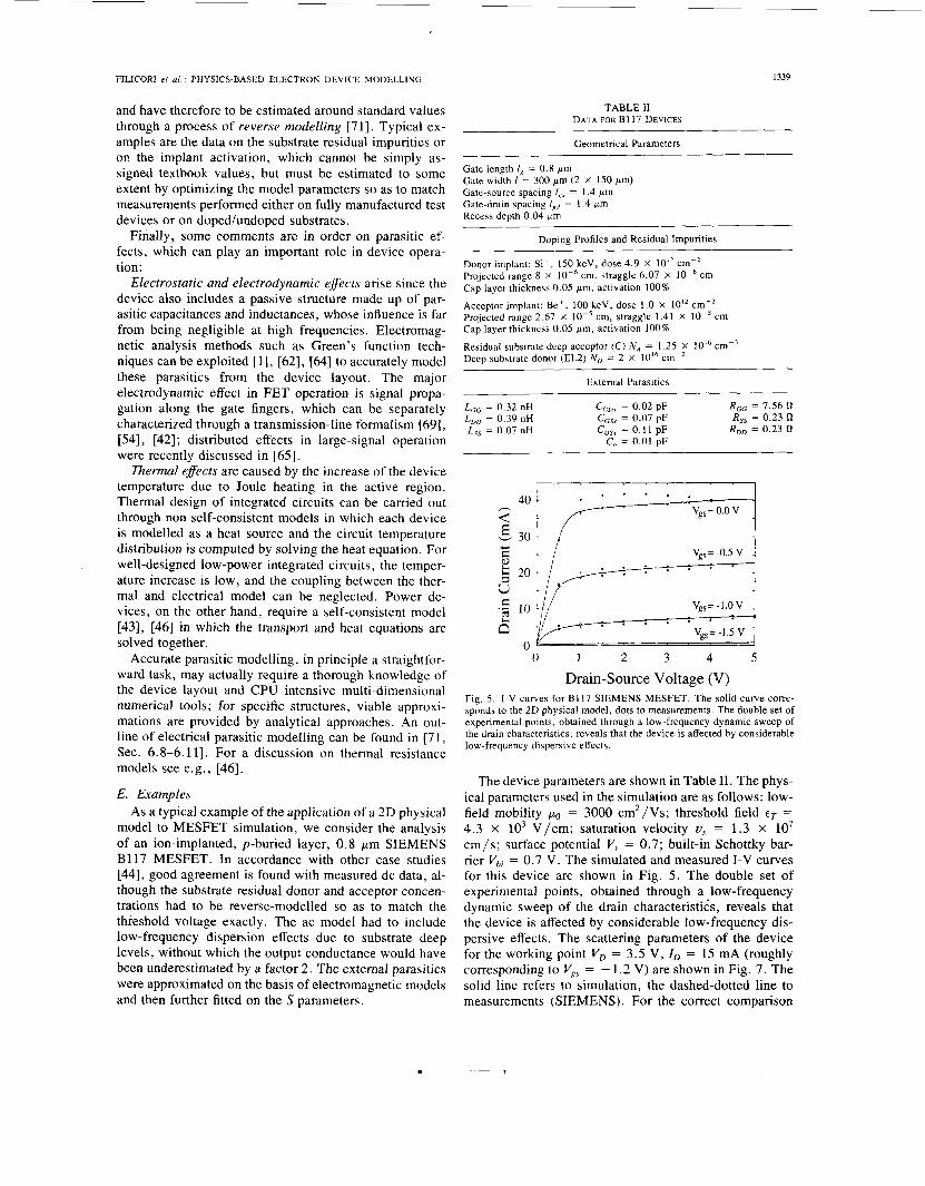
model to MESFET simulation, we consider the analysis of an ion-implanted, p-buried layer, 0.8 pm SIEMENS B117 MESFET. In accordance with other case studies [44], good agreement is found with measured dc data, al- though the substrate residual donor and acceptor concen- trations had to be reverse-modelled so as to match the threshold voltage exactly. The ac model had to include low-frequency dispersion effects due to substrate deep levels, without which the output conductance would have been underestimated by a factor 2. The extemal parasitics were approximated on the basis of electromagnetic models and then further fitted on the S parameters.
TABLE I1 DATA FOR B117 DEVICES
Geometrical Parameters
Gate length I , = 0.8 pm Gate width I = 300 pm (2 X 150 pm) Gate-source spacing I,, = 1.4 pm Gate-drain spacing IRd = 1.4 pm Recess depth 0.04 pm
Doping Profiles and Residual Impurities
Donor implant: Si’, 150 keV, dose 4.9 X 10” cm-* Projected range 8 X cm, straggle 6.07 X cm Csp layer thickness 0.05 pm, activation 100%
Acceptor implant: Be’, 100 keV, dose 1 .O X 10I2 cm-2 Projected range 2.67 X cm, straggle 1.41 X cm Cap layer thickness 0.05 pm, activation 100%
Residual substrate deep acceptor ( C ) N A = 1.25 X ?0l6 cm-3 Deep substrate donor (EL2) N D = 2 X l o i 6 cm-3
External Parasitics
L,, = 0.32 nH L , = 0.39 nH L,, = 0.07 nH
C,, = 0.02 pF CGsx = 0.07 pF CDsx = 0.11 pF CO = 0.01 pF
R,, = 7.56 a2 R, = 0.23 51
R,, = 0.23 n
‘ I / vgs=o.ov 1
0 1 2 3 4 5
Drain-Source Voltage (11) Fig. 5. I-V curves for BI 17 SIEMENS MESFET. The solid curve corre- sponds to the 2D physical model, dots to measurements. The double set of experimental points, obtained through a low-frequency dynamic sweep of the drain characteristics, reveals that the device is affected by considerable low-frequency dispersive effects.
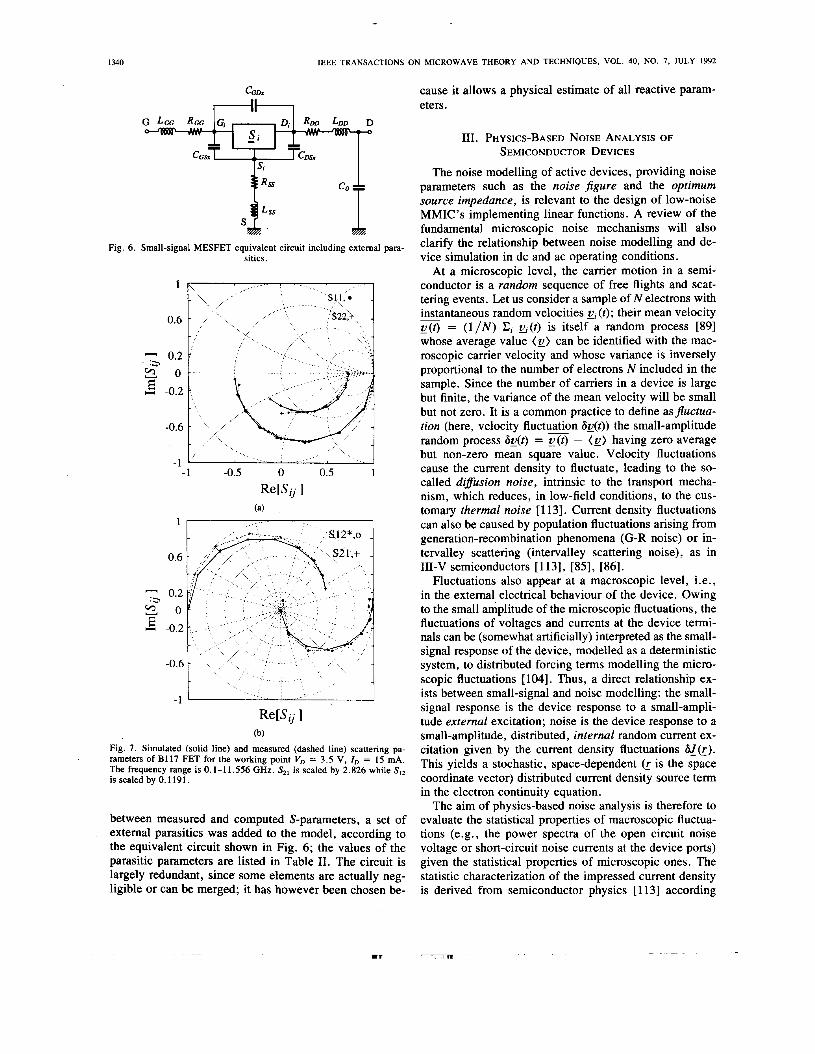
The device parameters are shown in Table 11. The phys- ical parameters used in the simulation are as follows: low- field mobility ,uo = 3000 cm2/Vs; threshold field cT = 4.3 x IO3 V/cm; saturation velocity U , = 1.3 X lo7 cm/s; surface potential V, = 0.7; built-in Schottky bar- rier Vbj = 0.7 V. The simulated and measured I-V curves for this device are shown in Fig. 5. The double set of experimental points, obtained through a low-frequency dynamic sweep of the drain characteristids, reveals that the device is affected by considerable low-frequency dis- persive effects. The scattering parameters of the device for the working point V, = 3.5 V, ID = 15 mA (roughly corresponding to Vgs = - 1.2 V) are shown in Fig. 7. The solid line refers to simulation, the dashed-dotted line to measurements (SIEMENS). For the correct comparison
1340 IEEE TRANSACTIONS ON MICROWAVE THEORY AND TECHNIQUES, VOL. 40, NO. 7, JULY 1992
1 T
Fig. 6. Small-signal MESFET equivalent circuit including external para- sitics.
1 S11,.
0.6
- 0.2 :> z o E U -0.2
-0.6
-1 -1 -0.5 0 0.5 1
R W i j 1 (a)
I
0.6
- . 0.2
z o E
.a
U -0.2
-0.6
-1 ' Re[Sij 1
(b) Fig. 7 . Simulated (solid line) and measured (dashed line) scattering pa- rameters of B117 FET for the working point VD = 3.5 V, ID = 15 d. The frequency range is 0.1-11.556 GHz. S,, is scaled by 2.826 while Slz is scaled by 0.1191.
between measured and computed S-parameters, a set of external parasitics was added to the model, according to the equivalent circuit shown in Fig. 6; the values of the parasitic parameters are listed in Table 11. The circuit is largely redundant, since some elements are actually neg- ligible or can be merged; it has however been chosen be-
cause it allows a physical estimate of all reactive param- eters.
111. PHYSICS-BASED NOISE ANALYSIS OF SEMICONDUCTOR DEVICES
The noise modelling of active devices, providing noise parameters such as the noise jgure and the optimum source impedance, is relevant to the design of low-noise MMIC's implementing linear functions. A review of the fundamental microscopic noise mechanisms will also clarify the relationship between noise modelling and de- vice simulation in dc and ac operating conditions.
At a microscopic level, the carrier motion in a semi- conductor is a random sequence of free flights and scat- tering events. Let us consider a sample of N electrons with instantaneous random velocities a ( t ) ; their mean velocity v(t) - = (1/N) Ci a ( t ) is itself a random process [89] whose average value ( E ) can be identified with the mac- roscopic carrier velocity and whose variance is inversely proportional to the number of electrons N included in the sample. Since the number of carriers in a device is large but finite, the variance of the mean velocity will be small but not zero. It is a common practice to define asjuctua- tion (here, velocity fluctuation Sg(t)) the small-amplitude random process SE@) = v(t) - ( E ) having zero average but non-zero mean square value. Velocity fluctuations cause the current density to fluctuate, leading to the so- called difision noise, intrinsic to the transport mecha- nism, which reduces, in low-field conditions, to the cus- tomary thermal noise [ 1 131. Current density fluctuations can also be caused by population fluctuations arising from generation-recombination phenomena (G-R noise) or in- tervalley scattering (intervalley scattering noise), as in 111-V semiconductors [ 1 131, [85], [86].
Fluctuations also appear at a macroscopic level, i.e., in the extemal electrical behaviour of the device, Owing to the small amplitude of the microscopic fluctuations, the fluctuations of voltages and currents at the device termi- nals can be (somewhat artificially) interpreted as the small- signal response of the device, modelled as a deterministic system, to distributed forcing terms modelling the micro- scopic fluctuations [ 1041. Thus, a direct relationship ex- ists between small-signal and noise modelling: the small- signal response is the device response to a small-ampli- tude external excitation; noise is the device response to a small-amplitude, distributed, internal random current ex- citation given by the current density fluctuations &I@). This yields a stochastic, space-dependent @ is the space coordinate vector) distributed current density source term in the electron continuity equation.
The aim of physics-based noise analysis is therefore to evaluate the statistical properties of macroscopic fluctua- tions (e.g., the power spectra of the open circuit noise voltage or short-circuit noise currents at the device ports) given the statistical properties of microscopic ones. The statistic characterization of the impressed current density is derived from semiconductor physics [ 1131 according
1 . -_
FILICORI et al.: PHYSICS-BASED ELECTRON DEVICE MODELLING 1341
to the noise mechanism considered, and is usually ex- pressed in the form of the correlation spectrum su(rl)6~(~) (n 3, U) = 6J (11, 0) U * (9, U), where the bar sign aind * denote, respectively, ensemble average and complex conjugate. Since the correlation length of micro- scopic fluctuations is of the order of the free mean path, these are often considered as spatially uncorrelated, i.e., S q r l ) ~ ( r 2 ) C r i 9 li, a) = KsruCr~, u)W~ - L ~ ) , where 9 is the-Dirac pulse function; K is usually referred to as local noise source [85]. For uncorrelated difusion noise [104, 1131 the local noise source is Kuu(_r, U) = 4q2Dono@) where Do and no are the workingpoint diffu- sivity matrix and electron density, respectively.
The small-signal potential fluctuations induced by
Gate -1 Drain
6J(L) can generally be expressed by means of the Green’s of the problem and of a superposition integral
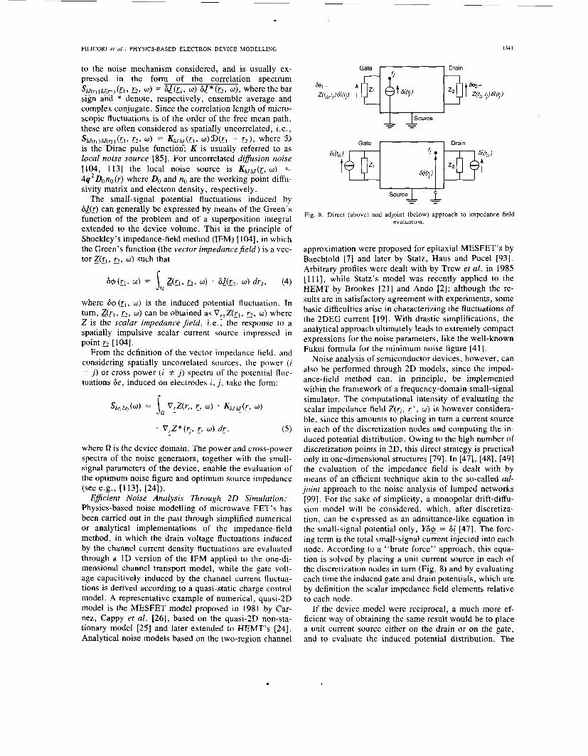
extended to the device volume. This is the principle of Shockley’s impedance-field method (IFM) [ 1041, in which the Green’s function (the vector impedance$&) is a vec- tor z(rl, K ~ , a) such that
Fig. 8 . Direct (above) and adjoint (below) approach to impedance field evaluation.
approximation were proposed for epitaxial MESFET’s by Baechtold [7] and later by Statz, Haus and Puce1 [93]. Arbitrary profiles were dealt with by Trew et al. in 1985
(4) [1111 while Statz’s model was recently applied to the HEMT by Brookes [21] and Ando [2]; although the re-
64 kl, U) = s, z(rl, 5, a) 9 6JJ(r2, U) dr2,
where 64 el, a) is the induced potential fluctuation. In turn, &, 5, U) can be obtained as V r l Z k I , 5, a) where Z is the scalar impedancejeld, i.e.; the response to a spatially impulsive scalar current source impressed in point 5 [ 1041.
From the definition of the vector impedance field, and considering spatially uncorrelated sources, the power (i = j ) or cross power (i # j ) spectra of the potential fluc- tuations 6e, induced on electrodes i , j , take the form:
Sse,se,(U) = S, v,zc~,, a> . K U ~ ( L , _ - U>
e VrZ*@, E, U) d r .
where Q is the device domain. The power and cross-power spectra of the noise generators, together with the small- signal parameters of the device, enable the evaluation of the optimum noise figure and optimum source impedance (see e.g., [113], [24]).
Eficient Noise Analysis Through 2 0 Simulation: Physics-based noise modelling of microwave FET’s has been carried out in the past through simplified numerical or analytical implementations of the impedance-field method, in which the drain voltage fluctuations induced by the channel current density fluctuations are evaluated through a 1D version of the IFM applied to the one-di- mensional channel transport model, while the gate volt- age capacitively induced by the channel current fluctua- tions is derived according to a quasi-static charge control model. A representative example of numerical, quasi-2D model is the MESFET model proposed in 1981 by Car- nez, Cappy et al. [26], based on the quasi-2D non-sta- tionary model [25] and later extended to HEMT’s [24]. Analytical noise models based on the two-region channel
sults are in satisfactory agreement with experiments, some basic difficulties arise in characterizing the fluctuations of the 2DEG current [ 191. With drastic simplifications, the analytical approach ultimately leads to extremely compact expressions for the noise parameters, like the well-known Fukui formula for the minimum noise figure [41].
Noise analysis of semiconductor devices, however, can also be performed through 2D models, since the imped- ance-field method can, in principle, be implemented within the framework of a frequency-domain small-signal simulator. The computational intensity of evaluating the scalar impedance field Z(r,, r ’ , U) is however considera- ble, since this amounts to placing in tum a current source in each of the discretization nodes and computing the in- duced potential distribution. Owing to the high number of discretization points in 2D, this direct strategy is practical only in one-dimensional structures [79]. In [471, [481, [491 the evaluation of the impedance field is dealt with by means of an efficient technique akin to the so-called ad- joint approach to the noise analysis of lumped networks [99]. For the sake of simplicity, a monopolar drift-diffu- sion model will be considered, which, after discretiza- tion, can be expressed as an admittance-like equation in the small-signal potential only, Y6@ = Si [47]. The forc- ing term is the total small-signal current injected into each node. According to a “brute force” approach, this equa- tion is solved by placing a unit current source in each of the discretization nodes in turn (Fig. 8) and by evaluating each time the induced gate and drain potentials, which are by definition the scalar impedance field elements relative to each node.
If the device model were reciprocal, a much more ef- ficient way of obtaining the same result would be to place a unit current source either on the drain or on the gate, and to evaluate the induced potential distribution. The
1342 IEEE TRANSACTIONS ON MICROWAVE THEORY AND TECHNIQUES. VOL. 40, NO. 7, JULY 1992
2.5
2
1.5 %
;z
2 150 1 8 3 100 LI 1
+measured - 1
2 4 6 8 10 12 14 16 18
Frequency, GHz (b)
C
8- 9 Y
f
350
300
250
200
150 I 0 measured
2 4 6 8 10 12 14 16 18
Frequency, GHz (C)
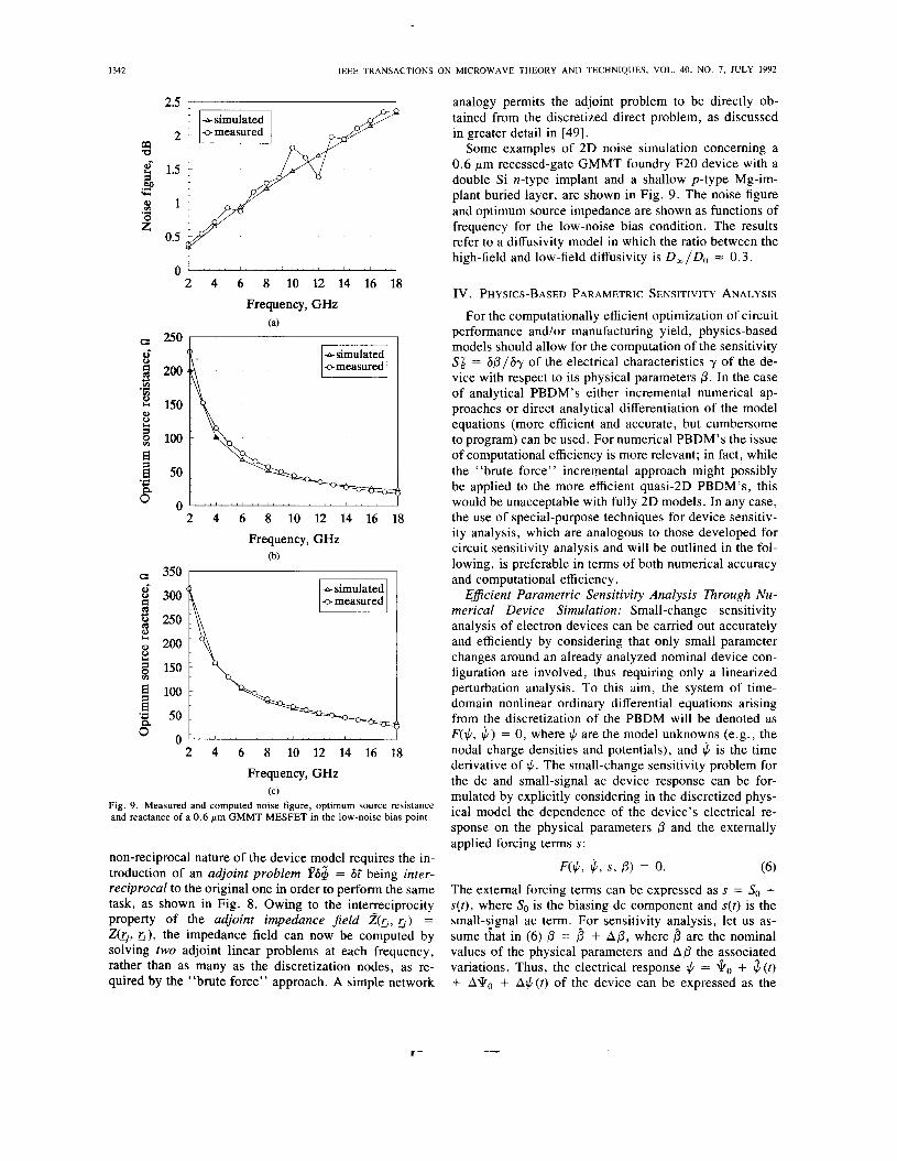
Fig. 9. Measured and computed noise figure, optimum source resistance and reactance of a 0.6 pm GMMT MESFET in the low-noise bias point.
non-reciprocal nature of the device model requires the in- troduction of an adjoint problem = Sc being inter- reciprocal to the original one in order to perform the same task, as shown in Fig. 8. Owing to the interreciprocity property of the adjoint impedance field .& 5 ) = Z ( 5 , c), the impedance field can now be computed by solving two adjoint linear problems at each frequency, rather than as many as the discretization nodes, as re- quired by the "brute force" approach. A simple network
analogy permits the adjoint problem to be directly ob- tained from the discretized direct problem, as discussed in greater detail in [49].
Some examples of 2D noise simulation concerning a 0.6 pm recessed-gate GMMT foundry F20 device with a double Si n-type implant and a shallow p-type Mg-im- plant buried layer, are shown in Fig. 9. The noise figure and optimum source impedance are shown as functions of frequency for the low-noise bias condition. The results refer to a diffusivity model in which the ratio between the high-field and low-field diffusivity is D m / D o = 0.3.
IV. PHYSICS-BASED PARAMETRIC SENSITIVITY ANALYSIS
For the computationally efficient optimization of circuit performance and/or manufacturing yield, physics-based models should allow for the computation of the sensitivity SJ = Sp/Sy of the electrical characteristics y of the de- vice with respect to its physical parameters @. In the case of analytical PBDM's either incremental numerical ap- proaches or direct analytical differentiation of the model equations (more efficient and accurate, but cumbersome to program) can be used. For numerical PBDM's the issue of computational efficiency is more relevant; in fact, while the "brute force" incremental approach might possibly be applied to the more efficient quasi-2D PBDM's, this would be unacceptable with fully 2D models. In any case, the use of special-purpose techniques for device sensitiv- ity analysis, which are analogous to those developed for circuit sensitivity analysis and will be outlined in the fol- lowing, is preferable in terms of both numerical accuracy and computational efficiency.
Eficient Parametric Sensitivity Analysis Through Nu- merical Device Simulation: Small-change sensitivity analysis of electron devices can be carried out accurately and efficiently by considering that only small parameter changes around an already analyzed nominal device con- figuration are involved, thus requiring only a linearized perturbation analysis. To this aim, the system of time- domain nonlinear ordinary differential equations arising from the discretization of the PBDM will be denoted as F($, $) = 0, where $ are the model unknowns (e.g., the nodal charge densities and potentials), and $ is the time derivative of $. The small-change sensitivity problem for the dc and small-signal ac device response can be for- mulated by explicitly considering in the discretized phys- ical model the dependence of the device's electrical re- sponse on the physical parameters p and the externally applied forcing terms s:
(6) The external forcing terms can be expressed as s = So + s( t ) , where So is the biasing dc component and s(t) is the small-?ignal ac term. For sensitivity analysis, let us as- sume that in (6) p = B + A p , where 0 are the nominal values of the physical parameters and A p the psociated variations. Thus, the electrical response II, = qo + $ ( t ) + A*,, + A $ ( t ) of the device can be expressed as the
F($, 4, s, 0) = 0.

FILICORI er al : PHYSICS-BASED ELECTRON DEVICE MODELLING 1343
superposition of dc (i.e., A*,) and small-sign!l ac (i.e., A$(t)) deviations from the nominal dc (i.e., qo) and ac (i.e., $(t)) responses. By differentiating (6), the following linearized sensitivity equation, which defines the varia- tions AQo of the dc device response in terms of small pa- rameter variations A 0, can be obtained [49] :
and very limited applications have so far been reported in the literature [52], (491, their importance in device and circuit optimization suggests that they will play a signif- icant role in the development of advanced CAD tools for MMIC design.
V. CIRCUIT PERFORMANCE ANALYSIS USING PHYSICS- a ,F . A’Po = -a,F * AD (7) BASED MODELS
where a,F is the gradient of F with respect to x, and all gradients :re evaluated at the nominal d,c bias point (i.e., for $ = \Eo, li/ = 0 , s = So, and p = P ) . Similarly, the sensitivity equation defining the variations A$ ( t ) of the small-signal ac device response caused by small parame- ter variations A 0 can be expressed, in the frequency do- main, in the form:
H . A% = - [asH - .i. + a’,,F. SI . ~ \ k ~
- [a,H * ?i. + a$F * SI AB (8)
where H = a,F + jwa,F, and S(w), $(U), !+(U) are, respectively, the Fourier transforms of s ( t ) , $ ( t ) , A$ ( t ) . The dc variation A*, in (8) is related to A 0 through the dc sensitivity relationship (7).
Equations (7) and (8) show that the variations in the dc and ac responses deriving from small variations in the physical parameters can be computed by solving two sys- tems of linearized incremental equations. This is a rela- tively inexpensive task, since the matrices 8, F in Eq. (7) and H in (8) coincide, respectively, with the Jacobian ma- trix for dc analysis and the coefficient matrix for small- signal ac analysis. Thus, once a complete device simula- tion has been carried out with nominal parameters, the solution of the small-change sensitivity equations (7) and (8) does not require any further LU factorization, but only forward and backward (FB) substitutions.
The computation of the whole sensitivity matrix SY, re- quires separate evaluation of the sensitivity to each pa- rameter pi , p2, . * , P N , which involves N forward and backward substitutions with as many different sets of pa- rameter perturbation vectors having all zero entries except a unit one. This can be computationally expensive when N is large. The same results can be obtained more effi- ciently by applying adjoint system techniques, which have been widely used for the sensitivity and noise analysis in electronic circuits [35], [9], [60], [99] and have recently been extended to the case of device analysis [49]. In these techniques advantage is taken of the properties of adjoint systems, which enable the computation of the sensitivity of a single electrical variable (e.g., the voltage or current at a given external contact) to all the parameters P k ’ s to be effected through a single FB substitution on the adjoint system of equations. Taking into account that the coeffi- cient matrix of the system is the transpose of the adjoint one, a simple FB substitution with a suitable right-hand term is sufficient for the complete parametric sensitivity analysis of an electrical variable at an external contact. Although sensitivity analysis techniques have only re- cently been introduced in the field of device modelling
In the physics-based approach to MMIC design, prob- lems related both to interfacing constraints with circuit analysis algorithms and to requirements on computing ef- ficiency must be faced. In fact, in most microwave CAD packages only behavioral models (e.g., experimentally- characterized nonlinear equivalent circuits or sets of measured S-parameters for small-signal analysis) are used to predict the electrical response of electron devices; be- havioral models, for both their high computational effi- ciency and their well-proven validity, are the most natural choice for circuit performance analysis. Computational ef- ficiency of models is particularly important when nonlin- ear circuit analysis is involved; this is the case not only in large-signal circuit analysis (usually based on har- monic-balance algorithms) but also in small-signal anal- ysis when the bias condition of electron devices must still be computed and/or optimally chosen. In such conditions a nonlinear model able to describe the electrical device response must be included and repeatedly used within the iterative loop needed for nonlinear analysis; thus, model linking and computational efficiency become relevant problems to be faced. To this aim, two different ap- proaches can be followed:
Direct linking of PBDM’s with nonlinear analysis al- gorithms;
Indirect finking of PBDM’s with non-linear circuit analysis through intermediate behavioral models.
Direct linking of PBDM’s with circuit analysis algo- rithms is clearly attractive for physics-based MMIC de- sign. However, repeated evaluation of the physical device equations during iteration-based nonlinear analysis limits the maximum affordable model complexity; thus, almost only the simpler analytical PBDMs (or behavioral models) can be practically embedded within non-linear analysis algorithms, provided that attention is given to ef- ficient implementation.
In fact, in most analytical PBDM’s some numerical procedures are still needed to enable the approximate so- lution of the physics-based device equations. For in- stance, in the model described in [68], an additional un- known (i.e., the internal potential V, ) must be numerically evaluated to predict the device response. In a straightfor- ward model implementation this involves an additional internal iterative loop within the non-linear analysis al- gorithm. It is preferable, instead, to deal with such un- knowns directly as additional variables in the circuit anal- ysis procedure; thus, nested iterative loops are not needed, while only a relatively small increase in the number of unknowns is involved. This computational expediency was adopted, according to 1121, for the harmonic-balance
1344 IEEE TRANSACTIONS ON MICROWAVE THEORY AND TECHNIQUES. VOL. 40, NO. 7. JULY 1992
analysis of a large-signal amplifier using the analytical model proposed by Trew [68].
Direct inclusion of numerical quasi-2D or 2D PBDM’s in non-linear circuit analysis algorithms is, at present, quite difficult. In fact, the few examples reported [ 1071 of large-signal amplifier analysis using numerical quasi-2D PBDM’s are limited to time-domain analysis of very sim- ple circuits, with a much lower complexity than that of typical MMIC’s. The need for the potentially more reli- able and accurate (see comments in Sec. II-B on model tuning) numerical PBDMs may derive from stronger re- quirements on predictive accuracy, possibly arising in performance- or yield-driven design of high performance MMIC’s. Better integration between device and circuit design phases can also be a valid reason for using numer- ical PBDM’s in MMIC performance analysis [45]; in this perspective, and in order to keep the number of time-con- suming numerical device simulations as low as possible, suitable computing strategies, based on intermediate be- havioral modelling, should be used for circuit perfor- mance analysis.
Indirect linking through intermediate behavioral models is a viable alternative to the direct use of PBDM’s in circuit analysis. In this approach, before starting circuit analysis, “off-line” numerical solution of the physics- based device equations is carried out over the whole op- erating region. This involves quite limited computing time (of the order of minutes on a medium-power PC [ 1 lo]) for the more efficient quasi-2D models; higher computa- tional effort (at least one order of magnitude), yet com- patible with the computing power of today’s more ad- vanced workstations, is needed by fully 2D device simulators. The results provided by the PBDM are then used (see Fig. 1) to derive a behavioral model (e.g., an equivalent circuit) to be included in the iterative nonlinear circuit analysis. This approach has the advantage of en- abling easier use of existing CAD tools for circuit analy- sis; moreover, efficient circuit analysis can be carried out without strongly restrictive contraints on the complexity of PBDM’s.
For physics-based MMIC design, efficient and repeat- able procedures are needed to derive the electrical param- eters of the associated behavioral model from numerical PBDM’s (model extraction). Both nonlinear equivalent circuits and special-purpose mathematical approaches can be used; the different linking and model extraction prob- lems will be examined in the following.
A. Nonlinear Equivalent Circuit Extraction from Numerical Physics-Based Models
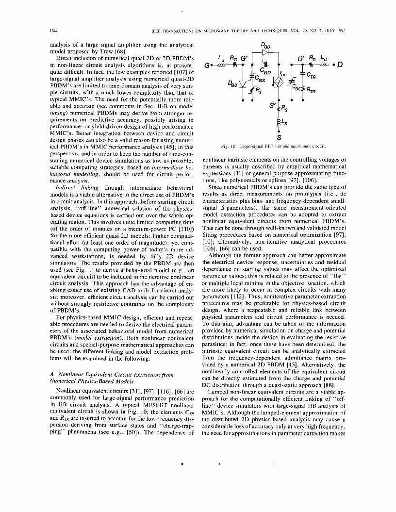
Nonlinear equivalent circuits [3 11, [97], [ 1 161, [66] are commonly used for large-signal performance prediction in HB circuit analysis. A typical MESFET nonlinear equivalent circuit is shown in Fig. 10; the elements CTR and RTR are inserted to account for the low-frequency dis- persion deriving from surface states and “charge-trap- ping” phenomena (see e.g., 1501). The dependence of
I- s’s% S
Fig. 10. Large-signal FET lumped equivalent circuit.
nonlinear intrinsic elements on the controlling voltages or currents is usually described by empirical mathematical expressions [3 11 or general-purpose approximating func- tions, like polynomials or splines 1971, 11061.
Since numerical PBDM’s can provide the same type of results as direct measurements on prototypes (i.e., dc characteristics plus bias- and frequency-dependent small- signal S-parameters), the same measurement-oriented model extraction procedures can be adopted to extract nonlinear equivalent circuits from numerical PBDM’s. This can be done through well-known and validated model fitting procedures based on numerical optimization 1971, [ 101 ; alternatively, non-iterative analytical procedures [106], 1661 can be used.
Although the former approach can better approximate the electrical device response, uncertainties and residual dependence on starting values may affect the optimized parameter values; this is related to the presence of “flat” or multiple local minima in the objective function, which are more likely to occur in complex circuits with many parameters [ 1 121. Thus, noniterative parameter extraction procedures may be preferable for physics-based circuit design, where a reapeatable and reliable link between physical parameters and circuit performance is needed. To this aim, advantage can be taken of the information provided by numerical simulation on charge and potential distributions inside the device in evaluating the resistive parasitics; in fact, once these have been determined, the intrinsic equivalent circuit can be analytically extracted from the frequency-dependent admittance matrix pro- vided by a numerical 2D PBDM [45]. Alternatively, the nonlinearly controlled elements of the equivalent circuit can be directly estimated from the charge and potential DC distribution through a quasi-static approach 1881.
Lumped non-linear equivalent circuits are a viable ap- proach for the computationally efficient linking of “off- line” device simulators with large-signal HB analysis of MMIC’s. Although the lumped-element approximation of the distributed 2D physics-based analysis may cause a considerable loss of accuracy only at very high frequency, the need for approximations in parameter extraction makes

FILICORI er al. : PHYSICS-BASED ELECTRON DEVICE MODELLING 1345
the functional link between physical parameters and cir- cuit performance not totally transparent. In such condi- tions, the computation of the sensitivity of the circuit re- sponse to physical parameters may become more difficult and less accurate. A possible alternative, which does not involve such limitations, can be provided by some re- cently proposed mathematical modelling approaches.
B. Mathematical Approaches to Nonlinear Behavioral Modelling of Electron Devices
New mathematical approaches 1391, [ 1001, 1331, [401 have been recently proposed for the behavioural non-lin- ear modelling of electron devices. The aim is to provide an accurate, technology-independent large-signal model which can be automatically and unambiguously derived from conventional measurements or numerical device simulations. In particular, the Nonlinear Integral Model (NIM) proposed in [39] and [40] seems to be particularly convenient for the efficient linking between numerical PBDMs and HB circuit analysis. The NIM is rigorously derived by modifying the well-known Volterra series [114], which has been widely used for the analysis and design of mildly nonlinear circuits 1781, [23], [75] , [58], [59]. Modifications are aimed at obtaining a mathematical formulation specially "oriented" to behavioral model- ing of electron devices, even under strongly nonlinear op- erating conditions. In fact, after describing in a voltage- controlled form the electrical device response through a conventional Volterra series, algebraic manipulations [40] lead to the following integral series:
P f
, t - 7,,)] and terms u(7) - u(t) instead of simply ~(7). This makes (9) efficient and easy to use (in spite of its apparent formal complexity) for the nonlinear perfor- mance prediction of electron devices. Unlike the classical Volterra series, this expansion does in fact provide fast convergence not only when mildly nonlinear phenomena are involved, but also when these are strong, provided that the practically finite duration 7, of nonlinear memory effects is relatively short (i.e., much shorter than the in- verse of the bandwidth of u(t)) . This can be intuitively understood by considering that in such conditions the terms u(7) - u(t) are small even when the voltage signal u has large amplitude.
Since the hypothesis of relatively short memory 7, for nonlinear phenomena is almost always satisfied for elec- tron devices when described in a voltage-controlled form2, fast convergence can be expected from the integral series (9), even in strongly nonlinear device operation. In fact, simulations and measurements on microwave transistors have shown [39], [40] that this integral series can be trun- cated, without significant loss of accuracy, at the first or- der nonlinear integral term. After series truncation, by considering discrete-spectrum signals and taking fre- quency-domain equivalence of time-domain convolution into account, (9) can be expressed in the harmonic-bal- ance-oriented form:
. . .
+ M
i(r) = Fdc[u(t)l + C P[u(t>, wkl VkeJUkf (10) k = -M
with: 7 m
P[u(t) , w l = 5 G"'[v( t ) , 71 [e- jw7 - 11 d ~ . (11)
* [u(71) - u(0l d71 According to the well-known HB formulation, the cur- rents i(r) and voltages v( t ) are related to their spectral components vk, 1, by the Fourier series:
f
+ j'j' G ~ ) [ u ( t ) , t - T I , t - T 2 I +M +M
f - 7 m v(r)= C I/ke'Wkf, i(t> = C I k e J w k r . (12)
The nonlinear function Fdc represents the dc character- istic of the device, while p i s a voltage-controlled strictly dynamic (as p = 0 for w = 0) admittance matrix which describes purely dynamic phenomena in the device's elec- trical behavior. This nonlinearly controlled matrix can be simply computed as a function of the bias-dependent small-signal parameters of a given device according to the
k = - M k = -M
' ['(71 ) - [u(72) - u(t)1 d71 d72
f
+ 5 5 s G'3'[u(t), t - T ~ , t - r2, t - ~~1
x [Y(TI) - u(Ol[0(72 1 - u(t)l
* [ V ( T ~ ) - ~ ( t ) ] d71 d72, d73 + . . .
f - 7 m
(9) expression [39], [40] : where i(t) and u(t) are the instantaneous voltage and cur- piu, = y[v,, - y[v,, o1 with ~ v, (13) rent at the device.'
The main difference between (9) and the classical Vol- terra series lies in the presence, within the convolution integrals, of voltage-dependent kemels G'"'[u(t) , r - 7,,
where Y[V, , w ] is the bias-voltage (V , ) and frequency- dependent (U) small-signal admittance matrix of the de- vice. Equations (10) and (13), together with (12), provide
'Equation (9) is valid for single-port devices; a more complex multi- variate expression can also be derived [40]. However, when the series in (9) is truncated at the single-fold integral, it can be directly used as a matrix expression for multi-port devices.
'The assumption of quasi-static charge distribution vs. applied voltage in electron devices, which has been successfully used in many device models, provides a qualitative explanation for this. More details are given in [40].
I346 IEEE TRANSACTIONS ON MICROWAVE THEORY A N D TECHNIQUES. VOL. 40, NO. 7, JULY 1992
a simple closed-form expression for the large-signal per- formance prediction of electron devices in terms of dc Characteristics and bias- and frequency-dependent small- signal admittance parameters; the hybrid form (i.e., both time- and frequency-domain) of (10) can be directly used with good computational efficiency in HB analysis algo- rithms.
Simulations and experimental results [39], [40] have confirmed the good accuracy of this nonlinear integral model in the large-signal performance prediction of GaAS MESFET’s. In particular, it has been used [40] as a com- putationally efficient link between a numerical 2D PBDM and a HB-based circuit analysis program. Good agree- ment was found between the results provided by (lo), (12), (13) (using the dc characteristics Fdc and bias-de- pendent small-signal Y-parameters provided by a 2D PBDM), and those obtained through a time-domain large- signal 2D device simulation (see Figs. 3 to 6 in [40]).
This approach has the advantages of being device-in- dependent and of not requiring any numerical procedure for parameter fitting, since no lumped-element approxi- mation of the device’s frequency-domain response is needed. Moreover, as the large-signal device response is described by closed-form expressions in terms of dc and ac electrical characteristics provided by a numerical PBDM, not only circuit performance but also its sensitiv- ity to physical parameters can be accurately and inexpen- sively computed, provided that efficient techniques for sensitivity analysis both at the device [49] and at the cir- cuit level [9], [60], [82] are exploited.
VI. COMPUTER-AIDED MMIC DESIGN USING PHYSICS-BASED DEVICE MODELS
The possibility of performance optimization in the space of physical device parameters is a sufficient reason to jus- tify the use of physics-based electron device models in MMIC design; however, more important reasons for the systematic use of PBDMs in MMIC design derive from requirements related to production yield. In fact, owing to the relatively low uniformity of GaAs technology, op- timizing the expected production yield can be practically more important than optimizing the ‘‘nominal” circuit performance (i.e., computed by neglecting technological uncertainties). To this aim, a number of Monte Carlo ap- proaches for yield estimation and iterative algorithms for its maximization have been proposed in the last few years [8], [96]. However, in order to realistically estimate cir- cuit production yield, suitable modelling approaches are also needed to simulate the statistical distributions of the random electrical characteristics of circuit components. To this aim, two different approaches can be used for sta- tistical device modelling:
The behavioral approach, where behavioural models (e.g., equivalent circuits or S-matrix descriptions) are sta- tistically Characterized through measurements on a set of prototype components. The set of measured data must be quite large in order to provide statistically significant in-
formation. Since any modification in the device structure implies a new statistical characterization, the possibilities of special-purpose tailoring of electron devices offered by the behavioural approach are very limited. Moreover, the statistics of electrical device parameters are described by complex and strongly correlated distributions. In fact, owing to the physical link between physical and electrical parameters, any deviation in a single physical parameter may strongly influence many different electrical device characteristics. This can be a problem for yield-driven de- sign, since in Monte Carlo analysis pseudo-random sets of parameter values with realistic distributions must be generated.
The physics-based approach, where deterministic physics-based models are associated to a statistical char- acterization of the physical parameter distributions deriv- ing from a given technological process. In this way, the limitations of the behavioural approach can be overcome; in fact, when a suitable PBDM provides a reliable deter- ministic link between physical and electrical device pa- rameters, only the statistics of the former need to be ex- perimentally characterized and numerically simulated. This is preferable not only because the physical parame- ters are relatively few, but also because these are either almost uncorrelated (e.g., gate length, doping profile, re- cessed depth of the same device) or subject to more pre- dictable correlations. Moreover, once a given technolog- ical process has been characterized, electrical performance statistics can be simulated for different device structures. This allows for statistical design centering with special- purpose “tailoring” of electron devices.
Experimental results in statistical modelling of GaAs MESFET’s [94], [95], [ 141, [6] seem to confirm the above considerations. In fact, complex and strongly correlated distributions have been found both for S-matrices and for the electrical parameters of statistically characterized equivalent circuits; thus, large experimental data bases seem to be necessary for realistic Monte Carlo simulation [94], [95], [5] when using statistical behavioural model- ling. On the other hand, PBDMs seem to provide realistic statistical predictions on the basis alone of a limited set of moments characterizing the simpler statistics of the physical parameters.
In particular, Anholt et al . [6], [5] have carried out a statistical characterization (both dc and ac parameters) for 400 MESFET samples manufactured by an MBE process; the physical device parameters (e.g., doping density, etching depth, gate length, etc.) generated by the MBE process were also statistically characterized through spe- cial-purpose measurement procedures. Monte Carlo sim- ulations, carried out through an analytical PBDM [3], [4] and using experimentally characterized Pearson distribu- tions for the physical parameters, showed reasonable agreement with the measured distributions of electrical parameters. For instance, the simulated and measured dis- tributions of the real part of SI, shown in Fig. 11 exhibit good overall agreement, apart from some slight discrep- ancy in the allocation of central values. Moreover, the
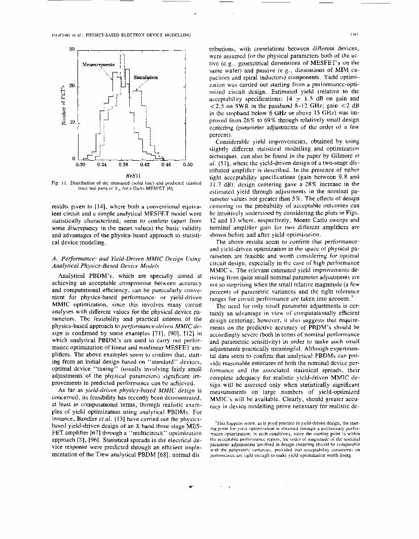
FILICORI et al.: PHYSICS-BASED ELECTRON DEVICE MODELLING 1347
30.
v1 20. F E %
I+
P 3 10.
0.
I ’ I ’ I ’ I ’
il ‘ I
Measurements ’ ’ \ I I r l
0.30 0.34 0.38 0.42 0.46 0.50
R e S l l Fig. 1 1 . Distribution of the measured (solid line) and predicted (dashed
line) real parts of SI, for a GaAs MESFET [ 6 ] .
results given in [ 141, where both a conventional equiva- lent circuit and a simple analytical MESFET model were statistically characterized, seem to confirm (apart from some discrepancy in the mean values) the basic validity and advantages of the physics-based approach to statisti- cal device modeling.
A. Performance- and Yield-Driven MMIC Design Using Analytical Physics-Based Device Models
Analytical PBDM’s, which are specially aimed at achieving an acceptable compromise between accuracy and computational efficiency, can be particularly conve- nient for physics-based performance- or yield-driven MMIC optimization, since this involves many circuit analyses with different values for the physical device pa- rameters. The feasibility and practical interest of the physics-based approach to performance-driven MMIC de- sign is confirmed by some examples [71], [90], [12] in which analytical PBDM’s are used to carry out perfor- mance optimization of linear and nonlinear MESFET am- plifiers. The above examples seem to confirm that, start- ing from an initial design based on “standard” devices, optimal device “tuning” (usually involving fairly small adjustments of the physical parameters) significant im- provements in predicted performance can be achieved.
As far as yield-driven physics-based MMIC design is concerned, its feasibility has recently been demonstrated, at least in computational terms, through realistic exam- ples of yield optimization using analytical PBDMs. For instance, Bandler et al. 1131 have carried out the physics- based yield-driven design of an X-band three-stage MES- FET amplifier [67] through a “multicircuit” optimization approach [SI, [96]. Statistical spreads in the electrical de- vice response were predicted through an efficient imple- mentation of the Trew analytical PBDM [68]; normal dis-
tributions, with correlations between different devices, were assumed for the physical parameters both of the ac- tive (e.g., geometrical dimensions of MESFET’s on the same wafer) and passive (e.g., dimensions of MIM ca- pacitors and spiral inductors) components. Yield optimi- zation was carried out starting from a performance-opti- mized circuit design. Estimated yield (relative to the acceptability specifications: 14 k 1.5 dB on gain and <2 .5 on SWR in the passband 8-12 GHz; gain < 2 dB in the stopband below 6 GHz or above 15 GHz) was im- proved from 26 % to 69 % through relatively small design centering (parameter adjustments of the order of a few percent).
Considerable yield improvements, obtained by using slightly different statistical modelling and optimization techniques, can also be found in the paper by Gilmore et al. [5 11, where the yield-driven design of a two-stage dis- tributed amplifier is described. In the presence of rather tight acceptability specifications (gain between 9.8 and 1 1.7 dB), design centering gave a 28% increase in the estimated yield through adjustments in the nominal pa- rameter values not greater than 5 %. The effects of design centering on the probability of acceptable outcomes can be intuitively understood by considering the plots in Figs. 12 and 13 where, respectively, Monte Carlo sweeps and nominal amplifier gain for two different amplifiers are shown before and after yield optimization.
The above results seem to confirm that performance- and yield-driven optimization in the space of physical pa- rameters are feasible and worth considering for optimal circuit design, especially in the case of high performance MMIC’s. The relevant estimated yield improvements de- riving from quite small nominal parameter adjustments are not so surprising when the small relative magnitude (a few percent) of parametric variances and the tight tolerance ranges for circuit performance are taken into account.
The need for only small parameter adjustments is cer- tainly an advantage in view of computationally efficient design centering; however, it also suggests that require- ments on the predictive accuracy of PBDM’s should be accordingly severe (both in terms of nominal performance and parametric sensitivity) in order to make such small adjustments practically meaningful. Although experimen- tal data seem to confirm that analytical PBDMs can pro- vide reasonable estimates of both the nominal device per- formance and the associated statistical spreads, their complete adequacy for realistic yield-driven MMIC de- sign will be assessed only when statistically significant measurements on large numbers of yield-optimized MMIC’s will be available. Clearly, should greater accu- racy in device modelling prove necessary for realistic de-
’This happens when, as is good practice in yield-driven design, the start- ing point for yield optimization is obtained through a preliminary perfor- mance optimization; in such conditions, since the starting point is within the acceptable performance region, the order of magnitude of the nominal parameter adjustments involved in design centering should be comparable with the parametric variances, provided that acceptability constraints on performance are tight enough to make yield optimization worth doing.
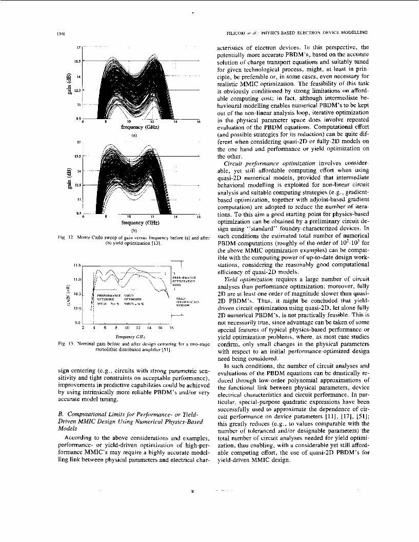
1348
9.5
FILICORI et al.: PHYSICS-BASED ELECTRON DEVICE MODELLING
I I 1 I I , , I
15.5 1 7 1
‘i 12.5 l4L
9.5 l l L
frequency (GHz)
(a)
8 IO 17. 14 16
frequency (GHz)
(b) Fig. 12. Monte Carlo sweep of gain versus frequency before (a) and after
(b) yield optimization [ 131.
sign centering (e.g., circuits with strong parametric sen- sitivity and tight constraints on acceptable performance), improvements in predictive capabilities could be achieved by using intrinsically more reliable PBDM’s and/or very accurate model tuning.
B. Computational Limits for Performance- or Yield- Driven MMIC Design Using Numerical Physics-Based Models
According to the above considerations and examples, performance- or yield-driven optimization of high-per- formance MMIC’s may require a highly accurate model- ling link between physical parameters and electrical char-
acteristics of electron devices. In this perspective, the potentially more accurate PBDM’s, based on the accurate solution of charge transport equations and suitably tuned for given technological process, might, at least in prin- ciple, be preferable or, in some cases, even necessary for realistic MMIC optimization. The feasibility of this task is obviously conditioned by strong limitations on afford- able computing cost; in fact, although intermediate be- havioural modelling enables numerical PBDM’s to be kept out of the non-linear analysis loop, iterative optimization in the physical parameter space does involve repeated evaluation of the PBDM equations. Computational effort (and possible strategies for its reduction) can be quite dif- ferent when considering quasi-2D or fully-2D models on the one hand and performance or yield optimization on the other.
Circuit performance optimization involves consider- able, yet still affordable computing effort when using quasi-2D numerical models, provided that intermediate behavioral modelling is exploited for non-linear circuit analysis and suitable computing strategies (e.g., gradient- based optimization, together with adjoint-based gradient computation) are adopted to reduce the number of itera- tions. To this aim a good starting point for physics-based optimization can be obtained by a preliminary circuit de- sign using ‘‘standard’ ’ foundry-characterized devices. In such conditions the estimated total number of numerical PBDM computations (roughly of the order of 102-103 for the above MMIC optimization examples) can be compat- ible with the computing power of up-to-date design work- stations, considering the reasonably good computational efficiency of quasi-2D models.
Yield optimization requires a large number of circuit analyses than performance optimization; moreover, fully 2D are at least one order of magnitude slower than quasi- 2D PBDM’s. Thus, it might be concluded that yield- driven circuit optimization using quasi-2D, let alone fully 2D numerical PBDM’s, is not practically feasible. This is not necessarily true, since advantage can be taken of some special features of typical physics-based performance or yield optimization problems, where, as most case studies confirm, only small changes in the physical parameters with respect to an initial performance-optimized design need being considered.
In such conditions, the number of circuit analyses and evaluations of the PBDM equations can be drastically re- duced through low-order polynomial approximations of the functional link between physical parameters, device electrical characteristics and circuit performance. In par- ticular, special-purpose quadratic expressions have been successfully used to approximate the dependence of cir- cuit performance on device parameters [ l l ] , [17], [51]; this greatly reduces (e.g., to values comparable with the number of toleranced and/or designable parameters) the total number of circuit analyses needed for yield optimi- zation, thus enabling, with a considerable yet still afford- able computing effort, the use of quasi-2D PBDM’s for yield-driven MMIC design.
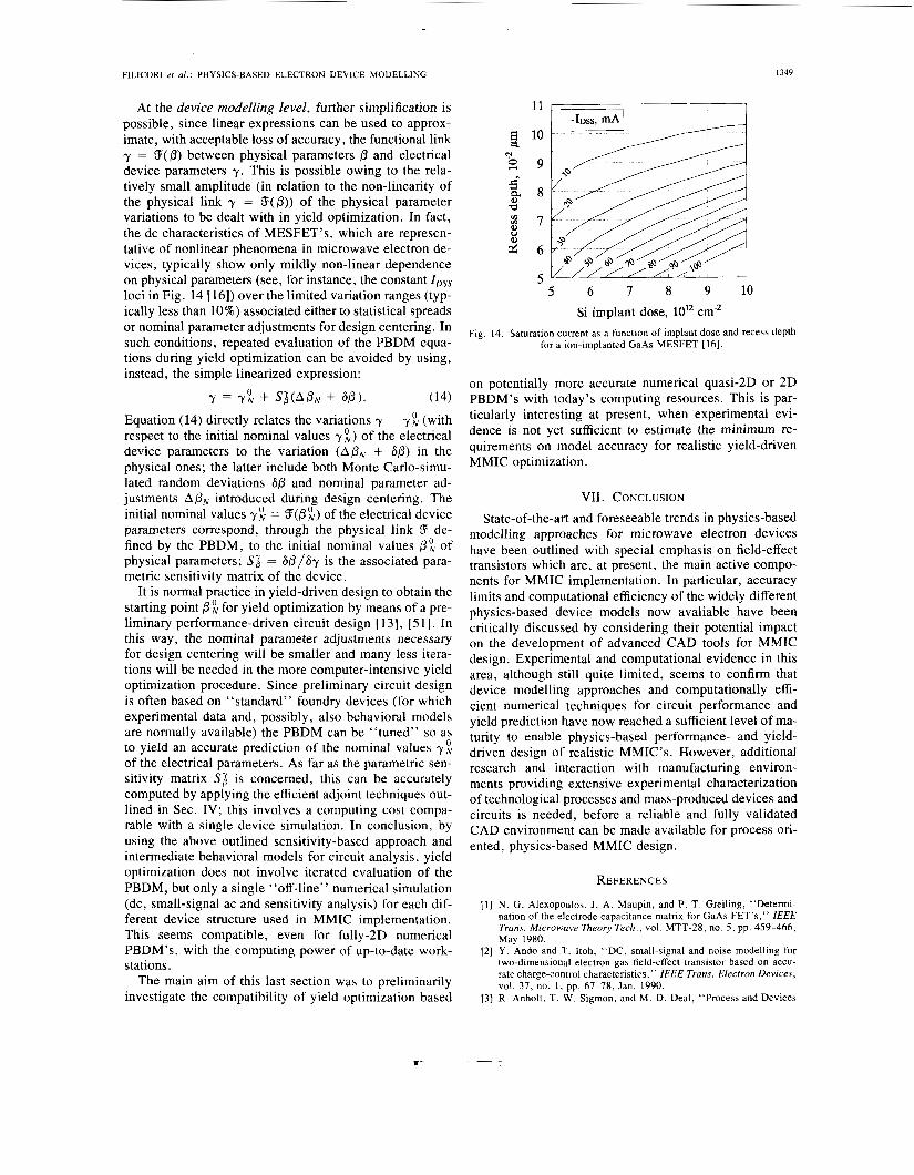
FILICORI er a l . : PHYSICS-BASED ELECTRON DEVICE MODELLING 1349
At the device modelling level, further simplification is possible, since linear expressions can be used to approx- imate, with acceptable loss of accuracy, the functional link y = S ( p ) between physical parameters @ and electrical device parameters y. This is possible owing to the rela- tively small amplitude (in relation to the non-linearity of the physical link y = 5(/3)) of the physical parameter variations to be dealt with in yield optimization. In fact, the dc characteristics of MESFET’s, which are represen- tative of nonlinear phenomena in microwave electron de- vices, typically show only mildly non-linear dependence on physical parameters (see, for instance, the constant ZD,, loci in Fig. 14 [16]) over the limited variation ranges (typ- ically less than 10%) associated either to statistical spreads or nominal parameter adjustments for design centering. In such conditions, repeated evaluation of the PBDM equa- tions during yield optimization can be avoided by using, instead, the simple linearized expression:
(14) Equation (14) directly relates the variations y - y i (with respect to the initial nominal values 7;) of the electrical device parameters to the variation (A@, + S@) in the physical ones; the latter include both Monte Carlo-simu- lated random deviations S o and nominal parameter ad- justments A b N introduced during design centering. The initial nominal values 7; = 5(/3;) of the electrical device parameters correspond, through the physical link 5 de- fined by the PBDM, to the initial nominal values @: of physical parameters; Sz = S@/Sy is the associated para- metric sensitivity matrix of the device.
It is normal practice in yield-driven design to obtain the starting point for yield optimization by means of a pre- liminary performance-driven circuit design [ 131, [5 11. In this way, the nominal parameter adjustments necessary for design centering will be smaller and many less itera- tions will be needed in the more computer-intensive yield optimization procedure. Since preliminary circuit design is often based on “standard” foundry devices (for which experimental data and, possibly, also behavioral models are normally available) the PBDM can be “tuned” so as to yield an accurate prediction of the nominal values y i of the electrical parameters. As far as the parametric sen- sitivity matrix Sz is concemed, this can be accurately computed by applying the efficient adjoint techniques out- lined in Sec. IV; this involves a computing cost compa- rable with a single device simulation. In conclusion, by using the above outlined sensitivity-based approach and intermediate behavioral models for circuit analysis, yield optimization does not involve iterated evaluation of the PBDM, but only a single “off-line” numerical simulation (dc, small-signal ac and sensitivity analysis) for each dif- ferent device structure used in MMIC implementation. This seems compatible, even for fully-2D numerical PBDM’s, with the computing power of up-to-date work- stations.
The main aim of this last section was to preliminarily investigate the compatibility of yield optimization based
y = y; + q ( A & + 60).
m m
8 2
11
10
9
8
7
6
5 - 5 6 7 8 9 1 0
Si implant dose, lo1’ cm-’ Fig. 14. Saturation current as a function of implant dose and recess depth
for a ion-implanted GaAs MESFET [ 161.
on potentially more accurate numerical quasi-2D or 2D PBDM’s with today’s computing resources. This is par- ticularly interesting at present, when experimental evi- dence is not yet sufficient to estimate the minimum re- quirements on model accuracy for realistic yield-driven MMIC optimization.
VII. CONCLUSION State-of-the-art and foreseeable trends in physics-based
modelling approaches for microwave electron devices have been outlined with special emphasis on field-effect transistors which are, at present, the main active compo- nents for MMIC implementation. In particular, accuracy limits and computational efficiency of the widely different physics-based device models now avaliable have been critically discussed by considering their potential impact on the development of advanced CAD tools for MMIC design. Experimental and computational evidence in this area, although still quite limited, seems to confirm that device modelling approaches and computationally effi- cient numerical techniques for circuit performance and yield prediction have now reached a sufficient level of ma- turity to enable physics-based performance- and yield- driven design of realistic MMIC’s. However, additional research and interaction with manufacturing environ- ments providing extensive experimental characterization of technological processes and mass-produced devices and circuits is needed, before a reliable and fully validated CAD environment can be made available for process ori- ented, physics-based MMIC design.
REFERENCES
[ I ] N . G. Alexopoulos, J . A. Maupin, and P. T. Greiling, “Detenn- nation of the electrode capacitance matrix for GaAs FET’s,” IEEE Trans. Microwave Theory Tech., vol. MTT-28, no. 5 , pp. 459-466, May 1980.
[2] Y . Ando and T. Itoh, “DC, small-signal and noise modelling for two-dimensional electron gas field-effect transistor based on accu- rate charge-control characteristics,” IEEE Trans. Electron Devices, vol. 37, no. 1, pp. 67-78, Jan. 1990.
[3] R. Anholt, T. W. Sigmon, and M. D. Deal, “Process and Devices

1350 IEEE TRANSACTIONS ON MICROWAVE THEORY AND TECHNICUES, VOL. 40, NO. 7 , JULY 1992
Models for GaAs MESFET technology,” in Tech. Dig. 1987 GaAs ICSymp., Portland, Oct. 1987, pp. 53-56.
[4] R. Anholt and T. W . Sigmon, “A process and device model for GaAs MESFET technology: GATES,” IEEE Trans. Computer- Aided Design, vol. 8, no. 4 , pp. 350-359, April 1989.
151 R. Anholt, R. Worley, and R. Neidhard, “Statistical analysis of GaAs MESFET S-parameter equivalent circuit models,” Int. J . Mi- crowave and Millimeter- Wave Computer-Aided Engineering, vol. l , no. 3, pp. 263-270, 1991.
[6] R. Anholt, J . King, R. Worley, and J . Gillespie, “Relationships between process and materials variations and variations in S- and equivalent-circuit parameters,” Int. J . Microwave and Millimeter- Wave Computer-Aided Engineering, vol. 1, no. 3, pp. 271-281, 1991.
[7] W. Baechtold, “Noise behaviour of GaAs field-effect transistors with short gate lengths,’’ IEEE Trans. Electron Devices, vol. ED-19, no. 5 , pp. 674-680, May 1972.
[8] J . W. Bandler and S . H. Chen, “Circuit optimization: The State of the Art,” IEEE Trans. Microwave Theory Tech., vol. 36, no. 2, pp. 424-442, Feb. 1988.
191 J . W. Bandler, Q. J . Zhang, R. M. Biernacki, “A unified, theory for frequency-domain simulation and sensitivity analysis of linear and nonlinear circuits,” IEEE Trans. on Microwave Theory Tech., vol. 36, no. 12, pp. 1661-1669, Dec. 1988.
[IO] 1 . W. Bandler, Q. J . Zhang, and S . H. Chen, “Efficient large-signal FET parameter extraction using harmonics,” IEEE Trans. Micro- wave Theory Tech., vol. 37, no. 12, pp. 2099-2108, Nov. 1989.
1111 J . W. Bandler, R. M. Biernacki, S . H. Chen, I . Song, S . Ye, and Q. J. Zhang, “Gradient quadratic approximation scheme for yield- driven design,” in 1991 IEEE M77-S Microwave Symp. Dig . , pp. 1197-1200.
[12] J. W. Bandler, Q. J . Zhang, and Q. Cai, “Nonlinear circuit opti- mization with dynamically integrated physical device models, ” in 1991 IEEE MTT-S Microwave Symp. Dig . , pp. 303-306.
[I31 J . W. Bandler, R. M. Biernacki, Q. Cai, S . H. Chen, S. Ye, and Q. J . Zhang, “Integrated physics-oriented statistical modeling, sim- ulation and optimization,” IEEE Trans. Microwave Theory Tech., vol. 40, no. 7, July 1992.
[I41 -, “Statistical modelling of GaAs MESFET’s,” in 1991 IEEE MTT-S Microwave Symp. Dig . , pp. 87-90.
[I51 T. M. Barton and P. H. Ladbrooke, “The role of the device surface in the high voltage behaviour of the GaAs MESFET,” Solid-State Electron., vol. 29, no. 8, pp. 807-813, 1986.
[16] A. Benvenuti, A. Cetronio, G. Ghione, R. Liberati, C . U. Naldi, and M . Pirola, “Physical simulation: a tool for technological eval- uation and optimization of GaAs MESFET devices,” in Proc. GAAS ’90, Rome, April 1990, pp. 96-101.
[I71 R. M. Biernacki, M. A. Styblinski, “Statistical circuit design with dynamic constraint approximation scheme,” in Proc. IEEE Int. Symp. on Circuits and Systems, 1986, pp. 941-944.
11 81 K. Blotekjaer, “Transport Equations for Electron in Two-Walley Semiconductors,” IEEE Trans. Electron Devices, vol. ED-17, no. 1, pp. 38-47, Jan. 1970.
[I91 E. Bonani, G. Ghione, and C. U. Naldi, “A CAD-oriented quasi- physical HEMT noise model for device design and optimization,” Proc. GAAS ’92, Nordwijk, Apr. 1992.
[20] P. Bonjour, R. Castagne, J-F. PBne, J-P. Courat, G. Bert, G. Nu- zillat, and M. Peltier, “Saturation mechanism in l-fim gate GaAs FET with channel-substrate interfacial bamer,” IEEE Trans. Elec- tron Devices, vol. ED-27, no. 6 , pp. 1019-1024, June 1980.
[21] T. M. Brookes, “The noise properties of high-electron mobility transistors,” IEEE Trans. Electron Devices, vol. ED-33, no. 1, pp. 52-57, Jan. 1986.
[22] F. A. Buot and J . Frey, “Effects of velocity overshoot on perfor- mance of GaAs devices, with design information, ” Solid-state Electron., vol. 26, no. 7 , pp. 617-632, 1983.
1231 J . Bussgang, L. Ehrman, and J . Graham, “Analysis of nonlinear systems with multiple inputs,” Proc. IEEE, vol. 62, no. 8, pp. 1088-1 119, Aug. 1974.
[241 A. Cappy, “Noise modelling and measurement techniques,” IEEE Trans. Microwave Theory Tech., vol. 36, no. 1, pp. 1-10, Jan. 1988.
1251 B. Camez, A. Cappy, A. Kaszynski, E. Constant, and G. Salmer, “Modelling of a submicrometer gate field-effect transistor including effects of nonstationary electron dynamics,” J . Appl. Phys., vol. 51, no. 1, pp. 784-790, Jan. 1980.
[26] B. Carnez, A. Cappy, R. Fauquembergue, E. Constant, and G. Sal- mer, “Noise modelling in submicrometer-gate FET’s MESFET,” IEEE Trans. Electron Devices, vol. ED-28, no. 7, pp. 784-789, July 1981.
[27] C:S. Chang and D.-Y. S . Day, “Analytic theory for current-volt- age characteristics and field distribution of GaAs MESFET’s,” IEEE Trans. Electron Devices, vol. 36, no. 2 , pp. 269-280, Feb. 1988.
[28] R. K. Cook and J . Frey, “Two-dimensional numerical simulation of energy transport effects in Si and GaAs MESFET’s,” IEEE Trans. Electron Devices, vol. ED-29, no. 6, pp. 970-977, June 1982.
1291 W. R . Curtice and Y. H. Yun, “A temperature model for the GaAS MESFET,” IEEE Trans. Electron Devices, vol. ED-28, no. 8, pp. 954-962, Aug. 1981.
[30] W. R. Curtice, “Direct comparison of the electron-temperature model with the particle-mesh (Monte-Carlo) model for the GaAS MESFET,” IEEE Trans. Electron Devices, vol. ED-29, no. 12, pp. 1942-1943, Dec. 1982.
[31] -, “GaAs MESFET modelling and nonlinear CAD,” IEEE Trans. Microwave Theory Tech., vol. MTT-36, no. 2, pp. 220-230, Feb. 1988.
1321 H. Daembkes, Ed., Modulation-Doped Field-Effect Transistors: Principle, Design and Technology, IEEE Press, 1990.
[33] R. R. Daniels, J . P. Harrang, and A. Yang, “A nonquasi-static, large signal FET model derived from small signal S-parameters,” Proc. ISDRS ’91, Charlottesville, VA, Dec. 1991, pp. 601-604.
1341 P. de Santis, “Extension of existing models to ion-implanted MES- FET’s,” IEEE Trans. Microwave Theory Tech., MTT-28, no. 6 , pp. 638-647, June 1980.
[35] S. W . Director and D. A. Rohrer, “Automated network design- The frequency-domain case,” IEEE Trans. Circuit Theory, no. 8, pp. 330-337, Aug. 1969.
[36] Y. K. Feng, “New u(E) Relationship of GaAs,” Electron. Lett., vol. 21, no. IO , May 1985, pp. 453-454.
[37] Y. K. Feng and A. Hintz, “Simulation of submicrometer GaAs MESFET’s using a full dynamic transport model,” IEEE Trans. Electron Devices, vol. 35, no. 9 , pp. 1419-1431, Sept. 1988.
[38] F . Filicori and V. A. Monaco, “Computer-aided design of non- linear microwave circuits,” Alfa Frequenza, vol. LVII, no. 7, pp. 355-378, Sep. 1988.
1391 F. Filicori and G. Vannini, “Mathematical approach to large-signal modelling of electron devices,” Electron. Lett., vol. 27, no. 4 , pp. 357-359, Feb. 1991.
[40] F. Filicori, V. A. Monaco, and G. Vannini, “A nonlinear integral model of electron devices for HB circuit analysis,” IEEE Trans. Microwave Theory Tech., IEEE Trans. Microwave Theory Tech., vol. 40, no. 7, July 1992.
1411 H. Fukui, “Optimal noise figure of microwave GaAs MESFET’s,” IEEE Trans. Electron Devices, vol. ED-26, no. 7, pp. 1032-1037, July 1979.
1421 G. Ghione and C. Naldi, “Modellieg and simulation of wave prop- agation effects in MESFET devices based on physical models,” in Proc. ESSDERC ’87, Bologna, Italy, Sept. 1987, pp. 317-320.
[43] G . Ghione, P. Golzio, and C. Naldi, “Self-consistent thermal modelling of GaAs MESFET’s: a comparative analysis of power device mountings,” Alfa Frequenza, pp. 31 1-319, Sept. 1988.
[44] G. Ghione, C. Naldi, F. Filicori, M. Cipelletti, and G . Locatelli, “MESS-A two-dimensional physical device simulator and its ap- plication to the development of C-band power GaAs MESFET’s,” Alfa Frequenza, pp. 295-309, Sept. 1988.
[45] -, “Physical modelling of GaAs MESFET’s in an integrated CAD environment: from device technology to microwave circuit perfor- mance,” IEEE Trans. Microwave Theory Tech., vol. 37, pp. 457- 468, Mar. 1989.
[46] G. Ghione and C. Naldi, “High-resolution self-consistent thermal modelling of multi-gate power GaAs MESFET’s,” in Proc. In:. El. Dev. Meeting ’89, pp, 6.5.1-4.
[47] G. Ghione, E. Bellotti, F . Filicori, “Physical c o k e modelling of majority-camer devices: an adjoint-network approach,” in Proc. Int. El. Dev. Meeting ’89, pp. 12.6.1-4.
[48] G. Ghione, “A two-dimensional approach to the noise simulation of GaAs MESFET’s,” in Proc. ESSDERC ’90, Nottingham, U .K. , Sept. 1990, pp. 225-229.
[49] G. Ghione and F . Filicori, “A computationally efficient unified ap- proach to the numerical analysis of the sensitivity and noise of semi- conductor devices, ” IEEE Trans. Computer-Aided Design, to be published.
FILICORI et a l . : PHYSICS-BASED ELECTRON DEVICE MODELLING 1351
[50] R. Goyal, M. Golio, and W. Thomann, “Low-Frequency Anom- alies in GaAs MESFET’s, Sec. 4.1.6.1. Monolithic Microwave In- tegrated Circuits, R. Goyal, Ed. Dedham, MA: Artech House, 1989.
[51] R. J . Gilmore, M. Eron, and T . Zhang, “Yield optimization of a MMIC distributed amplifier using physically-based device models, ” in 1991 IEEE M U - S Microwave Symp. Dig., pp. 1205-1208.
[52] A. Gnudi, P. Ciampolini, R. Guerrieri, M. Rudan, and G. Baccar- ani, “Sensitivity analysis for device design.” in Proc. ESSDERC ’87, Bologna, Italy, Sept. 1987, pp. 551-554, and IEEE Trans. Computer-Aided Design, vol. CAD-6, no. 5 , pp. 879-885, Sept. 1987.
1531 J . Graffeuil and P. Rossel, “Semi-empirical expression for direct transconductance and equivalent saturated velocity in short-gate length MESFET’s, Proc. IEE, vol. 129, pt. I, pp. 185-188, Oct. 1982.
[54] W. Heinrich and H. L. Hartnagel, “Wave propagation on MESFET electrodes and its influence on transistor gain,” IEEE Trans. Mi- crowave Theory Tech., vol. MTT-35, no. l , pp. 1-8, Jan. 1987.
[55] K. Hess, Advanced Theory of Semiconductor Devices. Englewood Cliffs, NJ: Prentice-Hall, 1988.
[56] J . A. Higgins, “Modelling the influence of carrier profiles on MES- FET characteristics,” IEEE Trans. Electron DeLVces, ED-27, no. 6 , pp. 1066-1073, June 1980.
[57] J . A. Higgins and D. N. Pattanayak, “A numerical approach to modelling the ultrashort gate MESFET,” IEEE Trans. Electron De- vices, vol. ED-29, no. 2, Feb. 1982.
[58] Y. Hu, J . Obregon, and J . C. Mollier, “Nonlinear analysis of mi- crowave FET oscillators using Volterra series,” IEEE Trans. Mi- crowave Theory Tech., vol. 37, no. l l , pp. 1689-1693, Nov. 1989.
[59] J. Baucells, A. Mediavilla, and A. Tazon, “Nonlinear analysis,” in GaAs MESFET Circuit Design, R. Soares Ed. Norwood, MA: Artech House, 1988.
1601 G. Iuculano, V . A. Monaco, and P . Tiberio, “Network sensitivities in terms of scattering parameters,” Electron. Lett., vol. 7 , pp. 53- 55, Jan. 1971.
1611 C. Jacoboni and P. Lugli, The Monte Carlo Methodfor Semicon- ductor Device Simulation.
[62] R. H. Jansen, “The Spectral-Domain Approach for Microwave In- tegrated Circuits,” IEEE Trans. Microwave Theory Tech.. vol. MTT-33, no. 10, pp. 1043-1056, Oct. 1985.
[63] R. H. Jansen, “LINMIC: a CAD package for the layout-oriented design of single- and multi-layer MICs/MMICs up to mm-wave fre- quencies,” MicrowaveJ., vol. 29, no. 2, pp. 151-161, 1986.
1641 -, “Advanced CAD/CAM software for process-related MMIC design,” Proc. ESA Workshop on MICs for Space Applications, Sec. 7/2. Mar. 1990, pp. 1-12.
1651 R. H. Jansen and P. Pogatzki, “Nonlinear distributed modelling of multifinger FET’slHEMT’s in terms of layout geometry and process data,” Proc. 21st Eur. Microwave Conf., 1991, pp. 609-614.
1661 A. K. Jastrzebsky, “MESFET modeling and parameter extraction,” in GaAs Technology and its Impact on Circuits and Systems. D. Haig and J . Everard, Eds.
1671 C. Kermarrec and C. Rumelhard, “Microwave monolithic inte- grated circuits,” in GaAs MESFET Circuit Design, R. Soares. Ed. Dedham, MA: Artech House, 1988, ch. 9 .
[68] M. A. Khatibzadeh and R. J. Trew, “A large-signal analytic model for GaAs MESFET,” IEEE Trans. Microwave Theon. Tech., vol. MTT-36, no. 2, pp. 231-238, Feb. 1988.
I691 R. L. Kuvas, “Equivalent circuit model of FET including distrib- uted gate effects,” IEEE Trans. Electron Devices, vol. ED-27, no. 6 , pp. 1193-1195, June 1980.
I701 P. H. Ladbrooke and S. R. Blight, “Low-field low-frequency dis- persion of transconductance in GaAs MESFET’s with implications for other rate-dependent anomalies,” IEEE Trans. Electron De- vices, vol. 35, no. 3, pp. 257-267, Mar. 1988.
(711 P. H. Ladbrooke, MMIC Design: GaAs FETs and HEMTs. Ded- ham, MA: Artech House, 1989.
[72] M. Lee, L. Forbes, T. Hallen, and P. Tuineega, “An analytical self-backgating GaAs MESFET model including deep-level trap ef- fects,” in Proc. Int. El. Dev. Meeting ’89, Dec. 1989, pp. 12.3.1- 12.3.4.
Berlin: Springer-Verlag, 1990.
London: Peregrinus, 1989.
[73] LIBRA, reference manual, EESsof Ind., 1989. [74] LINMIC + CAD Package, User Manual, Jansen Microwave, Ratin-
gen, Germany, 1989.
[75] S . A. Maas, Nonlinear microwave circuits. Dedham, MA: Artech House, 1988.
[76] A. Madjar and F. J . Rosenbaum, “A Large-Signal Model for the GaAs MESFET,” IEEE Trans. Microwave Theory Tech., vol. MTT- 29, no. 8, pp. 781-788, Aug. 1981.
[77] Microwave Harmonica, reference manual, Compact Software, Pa- terson, NJ.
[78] R . A. Minasian, “Large signal GaAS MESFET model and distor- tion analysis,” Electron. Lett., vol. 14, no. 6 , pp. 183-185, Mar. 1978.
[79] A. Moatadid, D. Gasquet, M. de Murcia, and G. P. Nougier, “Noise of GaAs diodes,” in Proc. ESSDERC ’1988, Montpellier, Sept. 1988, p. 583-586.
[80] M. S . Mock, Analysis of Mathematical Models of Semiconductor Devices. Dublin: Book Press, 1983.
[Sl] C . Moglestue, “A self-consistent Monte Carlo particle model to analyze semiconductor microcomponents of any geometry,” IEEE Trans. Computer-Aided Design, vol. CAD-5, no. 2, pp. 326-345, April 1986.
[82] V. A. Monaco and P. Tiberio, “Computer-aided analysis of micro- wave circuits,” IEEE Trans. Microwave Theory Tech., vol. MTT- 22, no. 3 , pp. 249-263, Mar. 1974.
1831 C. Naldi and F. Filicori, “QSS-Quick steady state analysis pro- gram,” European Space Agency Rep. No. 3334/77B, Pt. 2 , Jan. 1980.
(841 C. U. Naldi and G. Ghione, “Device simulation,” in III-V Micro- electronics, J . P. Nougier, Ed., vol. 2, European Materials Re- search Society Monographs, North Holland, 1991, pp. 89-1 14.
[ 8 5 ] J . P. Nougier, “Noise and diffusion of hot carriers,” in Physics of Nonlinear Transport in Semiconductors, D. K . Ferry, J . R. Barker, C . Jacoboni, Eds., New York: Plenum 1980, pp. 415-465.
[86] J . P. Nougier, “Origine du bruit dans les dispositifs B semiconduc- teurs,” Revue Phys. Appl., vol. 22, pp. 803-819, Aug. 1987.
[87] OSA90/hopeTM, reference manual, Optimization System Associates Inc., Dundas, ON, Canada, 1991.
[88] R. R. Pantoja, M. J . Howes, .I. R. Richardson, andC. M. Snowden, “A large-signal physical MESFET model for computer-aided de- sign and its applications,” IEEE Trans. Microwave Theory Tech., vol. MTT-37, no. 12, pp. 2039-2045, Dec. 1989.
1891 A. Papoulis, Probability, Random Variables, and Stochastic Pro- cesses. McGraw-Hill Kogakusha, 1965.
[90] D. Pavlidis, J-L. Cazaux, and J . Graffeuil, “The influence of ion- implanted profiles on the performance of GaAs MESFETs and MMIC Amplifiers,” IEEE Trans. Microwave Theory Tech., vol. 36,110. 4 , pp. 642-652, Apr. 1988.
[91] E. Pettenpaul, F. Ponse, 0. Berger, and H. Kapusta, “Device- physics and equivalent circuit model for GaAs MESFET’s Siemens Forsch.-u. Entwick1.-Ber., vol. 16, no. 5 , pp. 210-218, 1987.
[92] P. Pouvil, J.-L. Gautier, and D. Pasquet, “A new analytical model for the GaAs MESFET in the saturation region,” IEEE Trans. Elec- tron Devices, vol. ED-35, no. 8, pp. 1215-1222, Aug. 1988.
[93] R. A. Pucel, H. A . Haus, and H. Statz, “Signal and noise properties of gallium arsenide microwave field-effect transistors,” in Advances in Electronics and Electron Physics, vol. 38, New York: Academic,
[94] J . Purviance, D. Criss and D. Monteith, “FET model statistics and their effects on design centering,” in 1988 IEEE M7T-S Microwave Symp. Dig., p. 315, June 1988.
[95] J . Purviance, M. C. Petold and C. Potratz, “A linear statistical FET model using principal component analysis,” IEEE Trans. Micro- wave Theory Tech., vol. 36, no. 9 , pp. 1389-1395, 1989.
[96] J . Purviance and M. Meehan, “CAD for statistical analysis and de- sign of microwave circuits,” Int. J . Microwave and Millimter- Wave Computer-Aided Engineering, vol. 1 , no. 1, pp. 59-76, Jan. 1991.
[97] C. Rauscher, H. A. Willing, “Simulation of nonlinear microwave FET performance using a quasi-static model,” IEEE Trans. Micro- wave Theory Tech., vol. MTT-27, no. 10, pp. 834-840, Oct. 1979.
[98] V . Rizzoli, C. Cecchetti, A. Lipparini, and F . Mastri, “General- purpose harmonic balance analysis of nonlinear microwave circuits under multitone excitations,” IEEE Trans. on Microwave Theory Tech., vol. 36 , pp. 1650-1660, Dec. 1988.
1991 D. Rohrer, L. Nagel, R. Myer, and L. Weber, “Computationally efficient electronic-circuit noise calculation,” IEEE J . Solid-State Circuits, vol. SC-6, no. 4, pp. 204-212, Aug. 1971.
[loo] D. E. Root, S . Fan, and J . Meyer, “Technology-independent large-
1975, pp. 195-265.

1352 IEEE TRANSACTIONS ON MICROWAVE THEORY AND TECHNIQUES, VOL. 40, NO. 7, JULY 1992
signal non quasi-static models by direct construction from automat- ically characterized device data,” in Proc. 21st European Micro- wave Conf., Stuttgart, Sept. 1991, pp. 927-932.
[ l o l l P. A. Sandbom, J. R. East, and G. I. Haddad, “Quasi-two-dimen- sional modelling of GaAs MESFET’s,” IEEE Trans. Electron De- vices, vol. ED-34, no. 5 , pp. 985-991, May 1987.
1021 D. L. Scharfetter and H . K. Gummel, “Large signal analysis of a silicon read diode oscillator,” IEEE Trans. Electron Devices, vol. ED-16, no. 1, pp. 64-77, Jan. 1969.
1031 S. Selberherr, Analysis and Simulations of Semiconductor Devices. Berlin: Springer-Verlag. Wien 1984.
1041 W. Shockley, J. A. Copeland, and R. P. James, “The impedance field method of noise calculation in active semiconductor devices,” in Quantum Theory of Atoms, Molecules and Solid State, P. 0. Lowdin Ed.
[lo51 M. S. Shur, “Analytical model of GaAs MESFET’s,” IEEE Trans. Electron Devices, ED-25, no. 6 , pp. 612-618, June 1978.
11061 H . Sledzik and I. Wolf, “Large-signal modeling and simulation of GaAs MESFETs and HFETs,” Int. J . Microwave and Millimeter- Wave Computer-Aided Engineering, vol. 2, no. 1, pp. 49-60, 1992.
11071 C. M. Snowden, “Computer-aided design of MMIC’s based on physical device models,” Proc. Inst. Elec. Eng., vol. 133, pt. H ,
[IO81 C. M. Snowden and D. Loret, “Two-dimensional hot-electron models for short-gate length GaAS MESFET’s,” IEEE Trans. Elec- tron Devices, vol. ED-34, no. 2, pp. 212-223, Feb. 1987.
I1091 C. M. Snowden and R. R. Pantoja, “Quasi-two-dimensional sim- ulations for CAD,” IEEE Trans. Elecrron Devices, vol. ED-36, no. 9 , Sept. 1989.
[I101 C. M. Snowden, “Microwave and millimeter-wave device and cir- cuit design based on physical modelling,” Int. J . Microwave and Millimeter-Wave Computer-Aided Engineering, vol. 1, no. 1, pp. 4-21, Jan. 1991.
[ l l l ] R. J . Trew, M. A. Khatibzadeh, and N. A. Masnari, “Deep-level and profile effects upon low-noise ion-implanted GaAs MES- FET’s,” IEEE Trans. Electron Devices, vol. ED-32, no. 5 , pp. 877- 882, May 1985.
[ 1121 R. L. Vaitkus, “Uncertainty in the values of GaAs MESFET equiv- alent circuit elements extracted from measured two-port scattering parameters,” Proc. IEEE Cornell Conf. on High-speed Semicon- ductor Devices and Circuits, Aug. 1983, pp. 301-308.
[113] A. van der Ziel, Noise: Sources, Characterization, Measurements. Englewood, Cliffs, NJ: Prentice-Hall 1970.
[114] V. Volterra, Theory of Functionals and of Integral and Integro-Dif- ferential Equation New York: Dover, 1959.
[I151 C. K. Williams, T . H . Glisson, J . R. Hauser, M. A. Littlejohn, and M. F. Abusaid, “Two-dimensional Monte Carlo simulation of a submicron GaAs MESFET with a nonunifomly doped channel,” Solid-Stare Electron., vol. 28, no. 11, pp. 1105-1109, 1985.
11161 H. A. Willing, C. Rauscher, and P. De Santis, “A technique for predicting large-signal performance of a GaAs MESFET,” IEEE Trans. Microwave T h e o v Tech., vol. MTT-26, no. 12, pp. 1017- 1023, Dec. 1978.
[ 1171 K . Yamaguchi and H. Kodera, “Drain conductance of junction gate FET’s in the hot electron range,” IEEE Trans. Electron Devices, vol. ED-23, no. 6 , pp. 545-553, June 1976.
11181 K. Yamaguchi, S. Asai, and H . Kodera, “Two-dimensional nu- merical analysis of stability criteria of GaAs FET’s,” IEEE Trans. Electron Devices, vol. ED-23, no. 12, pp. 1283-1290. Dec. 1976.
New York: Academic Press, 1966. pp. 537-563.
pp. 419-427, Oct. 1986.
Fabio Filicori was bom in Imola, Italy in 1949. He received the Dr. Ing. degree in electronic en- gineering at the University of Bologna in 1974.
In the same year he joined the Department of Electronics of the University of Bologna, first as an Assistant Researcher and, later, as an Associ- ate Professor of Applied Electronics.
In November 1990 he became Full Professor of Applied Electronics at the University of Perugia. Last year he joined the Faculty of Engineering of the University of Ferrara, where he is Full Pro-
fessor responsible for the degree course in Electronic Engineering. During his academic career he has held courses on computer-aided circuit design, electron devices and circuits, and power electronics. His main research activities are in the areas of computer-aided design techniques for nonlinear microwave circuits, electron device modeling and electronic measure- ments.
Fabio Filicori is member of AEI (Associazione Elettrotecnica ed Elet- tronica Italiana).
Giovanni Ghione (M’87) received the Laurea de- gree in electronic engineering from Politecnico di Torino in 1981.
From 1983 to 1987 he was a Research Assistant at the Department of Electronics of the same Pol- itecnico. From 1987 to 1990 he was at Politecnico di Milano as an Associate Professor. In 1990 he joined the University of Catania as a Full Profes- sor in Solid-state Devices. His current research interests concern the numerical modelling of pas- sive and active components for hybrid and
monolithic (coplanar and multiconductor lines, -two-dimensional physical modelling of MESFET and HEMT devices, circuit-oriented nonlinear FET models) and the field of low-and high-frequency linear and nonlinear elec- tromagnetics.
Carlo U. Naldi (M’73-SM’89) graduated in elec- tronic engineenng from Politecnico di Tonno in 1967. In 1969 he became Assistant Professor of Applied Electronics, and then of Microwaves.
In 1970 he was also Professor in charge of Solid- State Electronic Devices In 1982 he became As- sociate Professor and then in 1986 Full Professor of Electronic Devices. Since 1967 he has been doing research at the Department of Electronics of the Politecnico di Tonno on high-frequency de- vice modelling and design. From 1977 he was in-
volved in several projects of the European Space Agency (ESA-ESTEC), mainly on harmonic-balance analysis of nonlinear microwave circuits, modelling and simulation of power GaAs MESFET’s, and automatic de- sign of MESFET amplifiers replacing TWTA Since 1984 he has been working on ESPRIT projects in the field of MMIC’s. His current research interests are in the area of modelling of active microwave devices for MMIC’s
Mr Naldi is member of the Amencan Physical Society and of the UMI (Italian Mathematical Association).