Review on Physically Flexible Nonvolatile Memory for Internet of Everything Electronics

596 IEEE TRANSACTIONS ON ELECTRON DEVICES, VOL. 59, NO. 3, MARCH 2012
Threshold Voltage Fluctuations in LocalizedCharge-Trapping Nonvolatile Memory Devices
Meir Janai, Member, IEEE, and Meng Chuan Lee
Abstract—Threshold voltage fluctuations are studied in lo-calized charge-trapping nonvolatile memory devices. Intensiveprogram/erase cycling followed by high-temperature bake shiftsthe mean Vt of programmed bits and increases the varianceof the Vt distribution. After long enough bake, the Vt decaysaturates, and the mean Vt and the variance stabilize. Uponcontinuing bakes, Vt’s of individual bits are found to fluctuateup and down while the envelope remains fixed. The formationof a stable envelope of randomly fluctuating bits is modeled interms of charge displacements of trapped electrons confined tothe cells’ nitride storage layer. Implications to product reliabilityunder high-temperature stress are discussed.
Index Terms—Charge trapping, nonvolatile memory (NVM)devices, stretched-exponential (SE) decay, threshold voltage insta-bility.
I. INTRODUCTION
B ROADENING of threshold voltage (Vt) distributions ofprogrammed bits under high-temperature storage condi-
tions was reported in both floating-gate (FG) and localizedcharge-trapping (LCT) nonvolatile memory (NVM) devices [1],[2]. The physical mechanism of distribution broadening andthe control of the distribution width are of importance for highreliability NVM devices, as broad Vt distributions degrade thedevice window of operation and may lead to premature dataretention failures.
In this paper, we report an experimental study of the in-stability of individual bits in LCT devices during long-termhigh-temperature storage, after intensive program/erase (P/E)cycling. Our study is performed on MirrorBit devices (seeFig. 1). In this class of devices, Vt instability due to stress-induced leakage current (Flash-SILC) is suppressed, no outlierbits are observed, and the Vt distributions are nearly Gaussianbefore and after thermal stress [2]. It enables clean study ofthe intrinsic mechanism of bit Vt fluctuations with minimuminterference of other mechanisms.
Previous studies of the broadening of Vt distributions due toindividual bit fluctuations were performed under experimentalconditions that caused the entire Vt distribution to shift whileit broadened [1], [2]. As the shift and the broadening simul-
Manuscript received September 6, 2011; revised December 6, 2011; acceptedDecember 8, 2011. Date of publication January 4, 2012; date of current versionFebruary 23, 2012. The review of this paper was arranged by Editor V. R. Rao.
M. Janai is with Spansion Israel Ltd., Netanya 42504, Israel (e-mail:[email protected]).
M. C. Lee is with Spansion Penang, 11900 Penang, Malaysia (e-mail: [email protected]).
Color versions of one or more of the figures in this paper are available onlineat http://ieeexplore.ieee.org.
Digital Object Identifier 10.1109/TED.2011.2180390
Fig. 1. Schematic of an LCT device. Programming and erase are done bychannel hot-electron (CHE) and tunnel-assisted hot-hole (TAHH) injections,respectively. The device is read by reversing the bias of the source (S) and thedrain (D). The distributions of the injected charges in the trapping layer arealso schematically shown.
taneously occur, it had been postulated that the same physicalmechanism is responsible for both the distribution broadeningand the Vt shift [2]. However, it has been also shown that, inLCT devices, the shift of the Vt distribution of programmed bitsafter P/E cycling follows a stretched-exponential (SE) decayfunction [2]–[4]. The decay of the SE function saturates wellabove the neutral state of the device. Hence, the question thatcomes up is, once the decay saturates and the envelope of the Vtdistribution stabilizes, do also individual bits reach steady-stateVt levels?
In this paper, we find that, even though the Vt distributionenvelope stabilizes, Vt’s of individual bits continue to ran-domly fluctuate up and down within the envelope. A modelexplaining the bounded bit-Vt fluctuations is presented, andthe significance of the results to product reliability under high-temperature stress (e.g., automotive applications) is discussed.
II. EXPERIMENTAL
A. General
The studied devices were selected from a 90-nm MirrorBitNOR Flash production line. These devices have a trappingOxide/Nitride/Oxide (ONO) sandwich with a tunnel oxidethickness of 7 nm, a 5-nm trapping nitride layer, and atotal ONO equivalent oxide thickness of 20.4 nm. Typicalprogramming bias conditions are source/gate/drain voltagesof 0/+9.5/+4 V, and typical erase bias conditions are float/−5/+5 V.
Bit Vt measurements were performed by scanning the word-line (control gate) voltage from low to high and reading the bits’current against a fixed reference level. Vt of a bit is defined asthe gate voltage at which the cell current of the bit equalizesthat of the reference (bit switches from pass to fail). The gatescanning voltage increments were 25 mV, hence, 6-V Vt scan
0018-9383/$31.00 © 2012 IEEE

JANAI AND LEE: THRESHOLD VOLTAGE FLUCTUATIONS IN LCT NVM DEVICES 597
Fig. 2. Experimental flow: (top diagram) preparation phase and (bottomdiagram) main experiment.
Fig. 3. Decay of the peak of the Vt distribution of the programmed (PGM)state of 1 Mbit distribution after fast 10,000 P/E cycles, with SE fit.
constituted 240 read operations. We verified that the reads up tothe highest scanning voltage do not inflict any Vt disturb of thebits. A Verigy V5000 tester was used for the measurements.
B. Preparation Phase
The experimental flow is shown in Fig. 2, with the prepara-tion phase described in the upper part of the diagram. Sectorsof 1.04 Mbit were cycled 10,000 P/E cycles within 30 h at am-bient temperature. This relatively fast cycling rate was appliedwithout any in-cycling relaxation, to accelerate the degradationeffect and bring out any resultant Vt instabilities. After cycling,the devices were programmed with a checker-board pattern andbaked 500 h at 150 ◦C.
Fig. 3 shows typical Vt traces at several storage temperaturesof the peak of 1 Mbit Vt distributions of a 128-Mb MirrorBitproduct after 10k cycles. The data is fitted to an SE function
V (t) = V t0 − ∆V tSAT ·[1 − e−(t/τ)β
](1)
where V to is Vt of the distribution peak at time t = 0;∆V tSAT = V t(t = 0) − V t(t = ∞); τ = τo · exp(Eτ/kBT );β = T/To; T is the temperature in degree K; kB is Boltzmannconstant; and τo, Eτ , and To are experimental fitting parameters
[2]. The SE fit in Fig. 3 exhibits saturation of the data retentionof cycled bits at a Vt level that is independent of bake tem-perature. This saturation feature was demonstrated in previousexperiments on similar devices [2]–[4]. The saturation featureis also confirmed by the experiments described below. The fitin Fig. 3 predicts that bake of 500 h at 150 ◦C will bring the Vtdistribution to within < 50 mV off its saturation value. Hence,this bake condition was selected for the preparation phase of theexperiment.
The P/E cycling conditions in Fig. 3 result in saturation ofthe decay of the Vt peak at 5.5 V, which is about 3 V above theneutral state. Other cycling conditions or product settings mightchange the value of V tSAT [4].
After the preparation phase, the product was not repro-grammed again throughout the entire experiment describedbelow.
C. Experiment
Following the preparation phase, the devices were consec-utively baked at 25 ◦C, 90 ◦C, 150 ◦C, 125 ◦C, and 175 ◦C,in the specified order of temperatures, for 100 h at eachtemperature. Each of the five bakes constitutes a “test.” Vtdistributions were taken at the beginning of each test and at 6,60, 600, and 6000 min of each test. All Vt measurements weretaken at room temperature. The 125 ◦C test was run after the150 ◦C test, to discriminate between aging effects that dependon the time sequence and temperature effects that depend onthe temperature sequence. In the data presented below, thetime scale restarts from 0 at the beginning of each new baketemperature (beginning of each “test”), even though the tests area continuous string of consecutive measurements on the sameensemble of bits. We tracked the Vt evolution as a functionof bake time of each bit individually throughout the five tests.In the analysis, we present the time evolution of the entiredistribution envelope, as well as changes of Vt of subgroupsof selected bits within that envelope.
III. RESULTS
Fig. 4 shows the Vt distribution after cycling, before andafter preparation bake. As shown, the preparation bake shiftsthe mean Vt of the distribution, VtMEAN, by approximately900 mV down, and the distribution width widens. Analysis ofthe data shows that σ increased from its initially programmedwidth of σ = 126 mV to σ = 154 mV.
Fig. 5 exhibits the Vt envelope of the 524K programmed-bitdistribution at all measurement points of the experiment. It isshown that the distribution envelope remains fixed at all timepoints at all temperatures, confirming the saturation of the SEfunction claimed above. The width of the distribution is alsoremarkably stable: the standard deviation at the beginning ofthe first RT test is 154.05 mV, and at the fifth test at 175 ◦C, itis 154.16, 153.71, 153.65, and 154.00 mV for the 0-, 6-, 60-,and 600-min bakes, respectively. We conclude that the overalldistribution width is stable throughout the entire experimentwithin experimental accuracy of ∆σ = +/ − 0.26 mV.

598 IEEE TRANSACTIONS ON ELECTRON DEVICES, VOL. 59, NO. 3, MARCH 2012
Fig. 4. Vt distribution after 10k cycles, before and after preparation bake of500 h at 150 ◦C. This product comes from the same process line as the productin Fig. 3 but is programmed to a different Vt window.
Fig. 5. Vt distributions of the bit envelope at all test points of the experiment.
Fig. 6. Vt trace of a typical bit throughout the experiment. x-axis indicatesthe time at each consecutive temperature.
Fig. 6 shows a Vt trace of a typical bit that, at the end of thepreparation phase, was at the center of the distribution envelope.It is shown that Vt of the bit fluctuates up and down withrandom walk characteristics. For the selected bit, |Vt − Vt(0)|for 25 ◦C and for 90 ◦C is bounded to within 50 mV, whereasat 150 ◦C and 175 ◦C, its fluctuations grow to 100 and 125 mV,respectively. At 125 ◦C, Fig. 6 does not show significant fluc-tuations, but one should recognize that the Vt measurementswere taken at specific time points, hence larger Vt fluctuationsat intermediate time points cannot be ruled out.
To study better the bit dynamics and statistical spread, we se-lected subgroups of bits that, at the beginning of each test, at t =0, had the same Vt value, denoted by Vtn. Each Vtn subgroupis initially represented by a near-delta function δ(Vt-Vtn).
In the following experiments, we report the evolution ofsigma of subgroups n, ∆σn,T (t), as a function of time t attemperature T . ∆σn,T (t) is calculated from
∆σ2n,T (t) = σ2
n,T (t) − σ2n,0 (2)
where σn,T (t) is the experimentally measured value of sigmaof subgroup n at time t, and σn,0 is the time-zero width ofsubgroup n. Limited tester accuracy, finite test increments, andvarious temporal noise sources such as sensing noise and RTN(random telegraph noise) caused the initial value of sigma ofeach subgroup to be σn,0 ≈ 26 mV. The initial value of σn,0
was determined by performing a Vt measurement at RT at thebeginning of each test. Few consecutive Vt measurements weremade before the first test to verify repeatability.
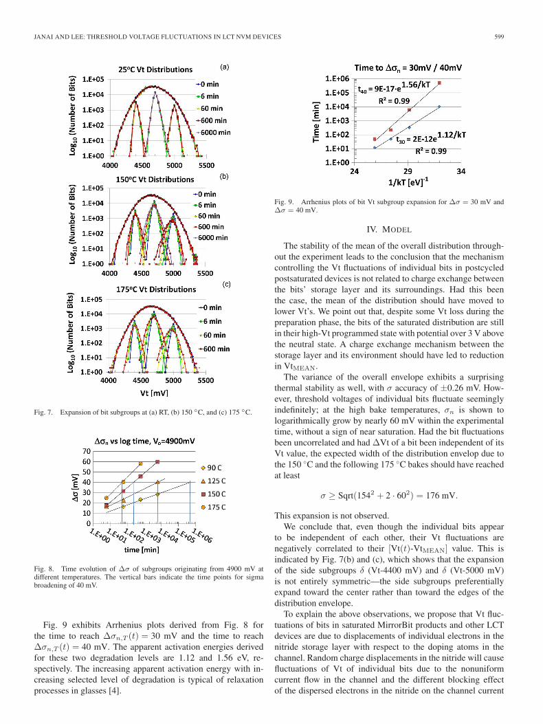
Fig. 7(a) exhibits three subgroups of the room temperaturetest, δ (Vt-4400 mV), δ (Vt-4700 mV), and δ (Vt-5000 mV)and the entire Vt envelope at different time points. It is shownthat the subgroups are as stable as their envelope, indicatingthat, at room temperature, σn,25C(t) ≈ σn,0 for at least up to100 h. Fig. 7(b) and (c) shows the evolution of subgroups atthe 150 ◦C test and the 175 ◦C test, respectively. We see that,at elevated temperature, the subgroups expand with time. It isfurther shown in Fig. 7(b) and (c) that, despite the apparentbroadening of the subgroups with time, the overall envelopedoes not change within ∆σ = ±0.26 mV, as stated above.
Fig. 8 shows the time evolution of ∆σn,T (t) of subgroupδ (Vt-4900 mV) at different bake temperatures. Nonparallellin–log plots are exhibited.
JANAI AND LEE: THRESHOLD VOLTAGE FLUCTUATIONS IN LCT NVM DEVICES 599
Fig. 7. Expansion of bit subgroups at (a) RT, (b) 150 ◦C, and (c) 175 ◦C.
Fig. 8. Time evolution of ∆σ of subgroups originating from 4900 mV atdifferent temperatures. The vertical bars indicate the time points for sigmabroadening of 40 mV.
Fig. 9 exhibits Arrhenius plots derived from Fig. 8 forthe time to reach ∆σn,T (t) = 30 mV and the time to reach∆σn,T (t) = 40 mV. The apparent activation energies derivedfor these two degradation levels are 1.12 and 1.56 eV, re-spectively. The increasing apparent activation energy with in-creasing selected level of degradation is typical of relaxationprocesses in glasses [4].
Fig. 9. Arrhenius plots of bit Vt subgroup expansion for ∆σ = 30 mV and∆σ = 40 mV.
IV. MODEL
The stability of the mean of the overall distribution through-out the experiment leads to the conclusion that the mechanismcontrolling the Vt fluctuations of individual bits in postcycledpostsaturated devices is not related to charge exchange betweenthe bits’ storage layer and its surroundings. Had this beenthe case, the mean of the distribution should have moved tolower Vt’s. We point out that, despite some Vt loss during thepreparation phase, the bits of the saturated distribution are stillin their high-Vt programmed state with potential over 3 V abovethe neutral state. A charge exchange mechanism between thestorage layer and its environment should have led to reductionin VtMEAN.
The variance of the overall envelope exhibits a surprisingthermal stability as well, with σ accuracy of ±0.26 mV. How-ever, threshold voltages of individual bits fluctuate seeminglyindefinitely; at the high bake temperatures, σn is shown tologarithmically grow by nearly 60 mV within the experimentaltime, without a sign of near saturation. Had the bit fluctuationsbeen uncorrelated and had ∆Vt of a bit been independent of itsVt value, the expected width of the distribution envelop due tothe 150 ◦C and the following 175 ◦C bakes should have reachedat least
σ ≥ Sqrt(1542 + 2 · 602) = 176 mV.
This expansion is not observed.We conclude that, even though the individual bits appear
to be independent of each other, their Vt fluctuations arenegatively correlated to their [Vt(t)-VtMEAN] value. This isindicated by Fig. 7(b) and (c), which shows that the expansionof the side subgroups δ (Vt-4400 mV) and δ (Vt-5000 mV)is not entirely symmetric—the side subgroups preferentiallyexpand toward the center rather than toward the edges of thedistribution envelope.
To explain the above observations, we propose that Vt fluc-tuations of bits in saturated MirrorBit products and other LCTdevices are due to displacements of individual electrons in thenitride storage layer with respect to the doping atoms in thechannel. Random charge displacements in the nitride will causefluctuations of Vt of individual bits due to the nonuniformcurrent flow in the channel and the different blocking effectof the dispersed electrons in the nitride on the channel current

600 IEEE TRANSACTIONS ON ELECTRON DEVICES, VOL. 59, NO. 3, MARCH 2012
Fig. 10. Schematic of a lateral charge displacement leading to a Vt fluctuation.
Fig. 11. Schematic of a localized electron displacement from over a lowcurrent-density area to over high current-density path, blocking the channelcurrent and increasing Vt of the bit.
[5]. However, because the electron displacements are confinedto the nitride storage layer, they will not shift VtMEAN of thedistribution envelope. We propose that, under thermal stress,the trapped electrons in the storage layer jump from one trap toanother within the nitride storage layer, thus modifying the Vtvalue of individual bits without changing VtMEAN.
Fig. 10 schematically shows a cross section of the device.Thermally activated electron excitation from over a low current-density path to over a high current-density path will lead toreduction in the cell current, which is interpreted as an increasein Vt of the nMOS device. The effect is further demonstrated inFig. 11, where an electron is schematically shown to jump fromover a low current-density path to over the main current-densitypath of the device’s channel.
The reason for the stable envelope is the low probability ofa cell to acquire a spatial combination of trapped electrons thatcauses an extreme Vt fluctuation. The envelope of the saturatedVt distribution is bounded by the statistical effect that prefers amore probable random arrangement of trapped electrons over arare spatial arrangement with respect to the doping atoms in thechannel. This statistical effect tends to shift bits preferentiallyfrom the edges of the distribution toward its center, resulting innegative correlation between the bits’ (Vt-VtMEAN) and ∆Vt,mentioned above.
The charge displacements in the trapping layer could haveled to horizontal charge escape from the cell, as the trappinglayer of the cell horizontally extends beyond the cell bound-aries. Such effect should have led to decay of VtMEAN, whichis not observed. We conclude that either the lateral charge trans-lations are very short, or, more likely, an electrostatic collectiveeffect is attracting the electrons in the storage layer to their
mirror-charge in the channel. A similar collective electrostaticeffect was employed to interpret simulation results of the widthof as-programmed distributions in charge-trapping devices [5].
V. DISCUSSION
RTN is regarded as a major source of Vt instability inmemory devices. Previous studies have suggested that the widthof bit distributions can change over time due to RTN [6],[7]. However, RTN cannot account for the increased widthof subgroup Vt’s reported here. Our RT test shows that timealone does not increase the width of the distributions, whichwould have been expected if RTN was the cause for the Vtfluctuations. Furthermore, in our postcycled high-temperatureexperiments, the interface states that are typically responsiblefor RTN [8] should have healed, hence reducing the RTNcontribution to the observed Vt fluctuations.
We conclude that, in saturated LCT devices, the evolution of∆Vt with time due to RTN is negligible. The RTN effect in ourdevices was accounted for by the initial value of σ0 that wassubtracted from the measured σn,T (t) results.
The current experimental results are consistent with the lat-eral dispersive transport model of charge carriers in the nitridelayer of LCT devices [2]–[4], [9]. That model was originallyproposed to explain the SE decay in NROM devices [2]–[4].The current experimental results, however, apply only to theconditions after the SE decay had stabilized. The current resultsdo not rule out other dominant mechanisms contributing to thedecay of Vt in the early phase of the SE decay [10]–[17].
Random fluctuations of Vt with similar variance (∼60 mV)were reported also for programmed bits in FG devices [1].In FG devices, the Vt fluctuations were attributed to small-number electron statistics, with negative Vt shifts attributed todetrapping of electrons from tunnel oxide traps to the substrateand positive Vt shifts attributed to electron detrapping andmigration from tunnel oxide traps to the FG. This explanationis unlikely in the LCT devices studied here because there isnot enough trapped charge in the tunnel oxide layer to accountfor the fluctuations shown, e.g., in Fig. 6. We point out thatour study was performed on fully annealed devices, hence theresidual trapped charge in the tunnel oxide layer is expectedto be negligible. In contrast, thermally activated distributionbroadening in FG devices was reported for devices whoseaverage Vt (i.e., the peak of the envelope) was also decaying,hence the study of FG does not represent a case of net zerocharge exchange between the storage layer and the substrate.We conclude that, during the initial (SE) decay phase, someholes and electrons trapped in the tunneling oxide may detrapand contribute to distribution broadening and individual bit Vtfluctuations, in accordance with the interpretation given fordistribution broadening in FG devices. However, once steady-state is reached, we believe the lateral charge displacements inthe trapping layer are the main source of Vt fluctuations.
VI. PRODUCT RELIABILITY CONSIDERATIONS
The experiments described above were conducted in aregime that is far beyond the requirements of normal consumer

JANAI AND LEE: THRESHOLD VOLTAGE FLUCTUATIONS IN LCT NVM DEVICES 601
products. With a cycling rate 1000 times faster than a user rate,which is estimated to accelerate the lifetime degradation bya factor of 10 and with apparent activation energy of 1.1 eV[3], [18] resulting in a thermal acceleration factor of 6525, the500 h of the preparation bake at 150 ◦C bring us to equivalentuser storage life of 3720 years at 55 ◦C. Even for indus-trial applications, the range we explored is beyond 137 yearsat 85 ◦C.
More relevant to the above experiments are applications thatrun at much higher temperatures, such as automotive under-the-hood applications. Our results indicate that, at the temperaturerange of 175 ◦C, Vt of LCT memory arrays is stable, and itsfluctuations are bounded. With proper selection of the operationwindow of the product, high reliability data retention can berealized.
ACKNOWLEDGMENT
The authors would like to thank I. Bloom, C. S. Law, andF.-Y. Soon for technical discussions and comments; M. Firozfor setting up the cycling test flow; and Z. M. Safar, N. Rajan,and S. Fan for technical support and data collection. MirrorBitis a registered trademark of Spansion Inc.
REFERENCES
[1] N. Mielke, H. Belgal, I. Kalastirsky, P. Kalavade, A. Kurtz, Q. Meng,N. Righos, and J. Wu, “Flash EEPROM threshold instabilities due tocharge trapping during program/erase cycling,” IEEE Trans. DeviceMater. Rel., vol. 4, no. 3, pp. 335–344, Sep. 2004.
[2] M. Janai, B. Eitan, A. Shappir, E. Lusky, I. Bloom, and G. Cohen, “Dataretention reliability model of NROM nonvolatile memory products,” IEEETrans. Device Mater. Rel., vol. 4, no. 3, pp. 404–415, Sep. 2004.
[3] M. Janai and B. Eitan, “The kinetics of degradation of data retention ofpost-cycled NROM non-volatile memory products,” in Proc. IEEE IRPS,2005, vol. 43, pp. 175–180.
[4] M. Janai, A. Shappir, I. Bloom, and B. Eitan, “Relaxation of localizedcharge in trapping-based nonvolatile memory devices,” in Proc. IEEE46th Int. Rel. Phys. Symp., 2008, pp. 417–423.
[5] A. Mauri, C. M. Compagnoni, S. M. Amoroso, A. Maconi, A. Ghetti,A. Spinelli, and A. L. Lacatia, “Comprehensive Investigation of statisti-cal effects in nitride memories—Part I: Physics-based modeling,” IEEETrans. Electron Devices, vol. 57, no. 9, pp. 2116–2123, Sep. 2010.
[6] C. M. Compagnoni, R. Gusmeroli, A. S. Spinelli, A. Lacaita,M. Bonanomi, and A. Visconti, “Statistical model for random telegraphnoise in flash memories,” IEEE Trans. Electron Devices, vol. 55, no. 1,pp. 388–395, Jan. 2008.
[7] M. Janai and I. Bloom, “Charge gain, NBTI recovery and random tele-graph noise in localized trapping NVM devices,” in Proc. IEEE Intern.Rel. Phys. Symp., 2011, pp. 819–823.
[8] C. M. Compagnoni, A. S. Spinelli, S. Beltrami, and A. Visconti, “Cyclingeffect on the random telegraph noise instabilities of NOR and NANDflash arrays,” IEEE Electron Device Lett., vol. 29, no. 8, pp. 941–943,Aug. 2008.
[9] A. Shappir, Y. Shacham-Diamand, E. Lusky, I. Bloom, and B. Eitan,“Lateral charge transport in the nitride layer of the NROM non-volatilememory device,” Microelectron. Eng., vol. 72, no. 1–4, pp. 426–433,Apr. 2004.
[10] T. Wang, W. J. Tsai, S. H. Gu, C. T. Chan, C. C. Yeh, N. K. Zous,T. C. Lu, S. Pan, and C. Y. Lu, “Reliability models of data retention andread-disturb in 2-bit nitride storage flash memory cells,” in IEDM Tech.Dig., Washington, DC, Dec. 2003, pp. 169–172.
[11] H. T. Lue, Y. S. Hsiao, Y. H. Shih, E. K. Lai, K. Y. Hsieh, R. Liu, andC. Y. Lu, “Study of charge loss mechanism of SONOS-type devices usinghot-hole erase and methods to improve the charge retention,” in Proc.IRPS, 2006, vol. 44, pp. 523–529.
[12] W. J. Tsai, N. K. Zous, H. Y. Chen, L. Liu, C. C. Yeh, S. Chen, W. P. Lu,T. Wang, J. Ku, and C. Y. Lu, “Investigation of charge loss in cycled NBitcells via field and temperature acceleration,” in Proc. IRPS, 2006, vol. 44,pp. 693–694.
[13] G. Tempel, R. Hagenbeck, and M. Strassburg, “Quantitative model fordata retention loss at NROM nitride charge trapping device after program/erase cycling,” in Proc. IEEE MSNVM, 2006, vol. 21, pp. 78–80.
[14] C. M. Compagnoni, C. Miccoli, R. Mottadelli, S. Beltrami, M. Ghidotti,A. L. Lacaita, A. S. Spinelli, and A. Visconti, “Investigation of the thresh-old voltage instability after distributed cycling in nanoscale NAND flashmemory arrays,” in Proc. IEEE Int. Rel. Phys. Symp., 2010, pp. 604–610.
[15] R. Daniel, A. Ruzin, and Y. Roizin, “Trap generation in cycled hot-electron-injection-programmed/hot-hole-erased silicon oxide–nitride–oxide–silicon memories,” J. Appl. Phys., vol. 99, no. 44, pp. 044 502/1–044 502/5, Feb. 2006.
[16] A. Shapira, Y. Shur, Y. Shacham-Diamand, A. Shappir, and B. Eitan,“Unified retention model for localized charge trapping nonvolatile mem-ory device,” Appl. Phys. Lett., vol. 92, no. 13, p. 133 514, Mar. 2008.
[17] A. Shapira, Y. Shur, Y. Shacham-Diamand, A. Shappir, and B. Eitan, “In-terface states formation in a localized charge trapping nonvolatile memorydevice,” J. Vac. Sci. Technol. B, , vol. 27, no. 1, pp. 508–511, Jan. 2009.
[18] Failure Mechanisms and Models for Semiconductor Devices, JEP122F,Nov. 2010.
Meir Janai (M’01) received the B.Sc. degree inphysics and mathematics from Hebrew University,Jerusalem, Israel, in 1968 and the M.Sc. and D.Sc.degrees in physics from the Technion-Israel Insti-tute of Technology, Haifa, Israel, in 1974 and 1977,respectively.
He is currently with Spansion Israel Ltd.,Netanya, Israel, as Senior Fellow, working on reli-ability physics of nonvolatile memory devices. Priorto joining Spansion, he was Vice President of Qual-ity and Reliability and VP of Operations at Saifun
Semiconductors. From 1985 to 2000, he was with Chip Express Corporation,Santa Clara, CA, holding the positions of Chief Scientist, VP of Quality,and Director of Business Development. From 1977 to 1984, he was a SeniorResearch Associate with the Department of Physics, Technion, IIT, and aVisiting Professor with the Optical Science Center, University of Arizona,Tucson. He is the holder of 18 U.S. patents and has 50 publications in the fieldsof nonvolatile memory reliability, amorphous semiconductors, solar energyconversion, and laser material processing.
Dr. Janai served as a member of the Israeli National Committee for Micro-electronics Foundations and was member of various technical review boards inIsrael and in the United States.
Meng Chuan Lee received the B.Eng. degreein electronics engineering, majoring in computers,from Multimedia University, Malaysia, where heis currently working toward the M.Eng. degree inmicroelectronics.
From 2006 to 2009, he worked as Product De-velopment Engineer with Spansion Penang, Penang,Malaysia, focusing on silicon debug and waferlevel characterization. Since March 2009, he hasbeen working as Reliability Engineer with SpansionPenang, focusing on NVM reliability issues and new
reliability stress test development.
Copyright © 2022 FDOKUMEN