Physically-Based Real-Time Diffraction Using Spherical Harmonics

Electronics 2015, 4, 424-479; doi:10.3390/electronics4030424
electronics ISSN 2079-9292
www.mdpi.com/journal/electronics
Review
Review on Physically Flexible Nonvolatile Memory for Internet of Everything Electronics
Mohamed T. Ghoneim and Muhammad M. Hussain *
Integrated Nanotechnology Lab, Electrical Engineering, Computer Electrical Mathematical Science
and Engineering Division, King Abdullah University of Science and Technology (KAUST),
Thuwal 23955-6900, Saudi Arabia; E-Mail: [email protected]
* Author to whom correspondence should be addressed;
E-Mail: [email protected]; Tel.: +966-544-700-072.
Academic Editor: Mohan Jacob
Received: 6 June 2015 / Accepted: 14 July 2015 / Published: 23 July 2015
Abstract: Solid-state memory is an essential component of the digital age. With
advancements in healthcare technology and the Internet of Things (IoT), the demand for
ultra-dense, ultra-low-power memory is increasing. In this review, we present a
comprehensive perspective on the most notable approaches to the fabrication of physically
flexible memory devices. With the future goal of replacing traditional mechanical hard
disks with solid-state storage devices, a fully flexible electronic system will need two basic
devices: transistors and nonvolatile memory. Transistors are used for logic operations and
gating memory arrays, while nonvolatile memory (NVM) devices are required for storing
information in the main memory and cache storage. Since the highest density of transistors
and storage structures is manifested in memories, the focus of this review is flexible NVM.
Flexible NVM components are discussed in terms of their functionality, performance
metrics, and reliability aspects, all of which are critical components for NVM technology
to be part of mainstream consumer electronics, IoT, and advanced healthcare devices.
Finally, flexible NVMs are benchmarked and future prospects are provided.
Keywords: flexible electronics; silicon; nonvolatile memory; ferroelectric; memristor;
resistive; flash; phase change memory; random access memory (RAM); transistor; CMOS;
inorganic; reliability
OPEN ACCESS

Electronics 2015, 4 425
1. Introduction
Recent advancements in flexible electronics research will enable novel applications ranging from
stylish flexible gadgets for real-time monitoring of health-related vital signs to novel biological
applications such as electronic skin [1–11]. Critical advances have been made in recent years that rely
on organic materials as active elements because of their inherent flexibility. Mainstream approaches to
capitalize on naturally flexible substrates like polymers can be categorized into (i) all-organic systems,
where both devices (specifically active materials) and substrates are made up of organic
materials [12–18] or inkjet- and screen-printed in thin layers onto paper and organic substrates [19–22]
and (ii) hybrid systems, where inorganic electronic devices are transferred onto an organic substrate
using transfer printing and other transfer techniques [23–31], laser lift-off transfer [32], and
low-temperature direct deposition of inorganic devices on plastic organic substrates [33–36]. Other
approaches use silicon-on-insulator (SOI) substrates, and controlled spalling technology to peel-off
thin semiconductor layers [37–39]. In addition, a complementary transfer-free approach has recently
been introduced, where thinning down the inorganic substrate through traditional, standard fabrication
processes improves the flexibility of the substrate [40–45].
These approaches are all geared towards achieving fully flexible electronic systems. The three main
components in any electronic system are (1) processing units; (2) the main memory; and (3) storage.
Processing units perform logic operations through transistor logic, while the main memory performs
temporary short-term storage (cache) with a quick access feature, also known as primary storage or
random access memory (RAM), through access transistors and capacitors that store charges. Storage
refers to the long-term retention of information, traditionally implemented using hard disks. However,
at present, a shift towards other NVM types in a solid-state drive (SSD) format for supporting faster
performance and higher integration densities within strict area constraints is taking place. Hence, the
main electronic devices required to build an electronic system are transistors, capacitors, and NVM
devices. Emerging NVM such as resistive random access memory (ReRAM), flash memory, phase
change RAM (PCRAM), and ferroelectric random access memories (FeRAMs) have the benefits of
fast switching, low-operation voltage, and ultra-large-scale-integration (ULSI) densities. These
attractive qualities not only make them a favorable option for replacing magnetic hard disks but also
for replacing quick access, volatile, dynamic RAM. This means that future electronic systems will
require combinations of only two essential devices: transistors and NVM devices.
An objective assessment of the discussed mainstream and complementary approaches to flexible
electronics must focus on their ability to provide high-performance, reliable NVM devices with ULSI
density transistors. In this review, we present the mainstream NVM architectures and technologies
with a special focus on most up-to-date techniques for producing flexible NVM devices.
Every memory cell consists of a gating device for access/select that is usually implemented using a
transistor. Hence, memory arrays are where the largest number of transistors exist in an electronic
system, a consequence of their ULSI density and low cost/bit ($/bit). Furthermore, with the continuous
reduction in $/bit of NVMs and the higher switching speeds between memory states (‘0’ to ‘1’ or vice
versa) of emerging NVM technologies, replacing volatile random access memory and magnetic hard
disks with faster SSDs made up of transistors and NVM structures becomes feasible. Here, the
progress made over the past few years in three prominent types of flexible NVM technologies is

Electronics 2015, 4 426
discussed: (i) resistive; (ii) ferroelectric; (iii) phase change; and (iv) charge-trapping NVMs. In
addition, the reliability aspects of the devices reported are discussed and an assessment for emerging
technologies that provides useful insights towards their potential for commercialization is also provided.
Figure 1 briefly positions the focus of this review in context with flexible electronics research.
Figure 1. Chart highlighting the focus of the review.
In this review, our discussion is restricted to works that demonstrated an actual flexible version of
flexible rewriteable NVMs between January 2010 and May 2015. However, there are many interesting
works on flexible write-once-read-multiple (WORM) NVMs and other NVM devices that might be
suitable for future applications in flexible electronics [46–51]. Furthermore, multiple interesting review
papers are available on non-volatile memory technologies; however, the comprehensive scope of this
review combining various flexing approaches, non-volatile memory and transistor technologies,
arraying architectures with a special focus on flexibility, performance, reliability and monolithic
integration ability has not been reported to date. For instance, Chung et al. [52], Makarov et al. [53],
and Wang et al. [54] reviewed NVM devices but flexibility was not addressed. Naber et al. [55],
Wang et al. [56], Liu et al. [57], and Chou et al. [58] reviewed only organic NVM. J.-S. Lee reviewed
floating gate NVM devices [59]. Lee and Chen [60], Jeong et al. [61], Panda et al. [62], Lin et al. [63],
Porro et al. [64], and Seok et al. [65] reviewed only resistive (ReRAM) NVM. Kim et al. reviewed
hybrid organic/inorganic nanocomposites materials for NVM [66]. Liu et al. [67] and Mai et al. [68]
reviewed only ferroelectric NVM and ferroelectric electronics. Kurosawa et al. reviewed polyamide

Electronics 2015, 4 427
based memory [69]. Han et al. reviewed various flexible NVM technology but reliability issues,
flexible access and logic transistors, and monolithic integration ability were not addressed [70].
Acharyya et al. reviewed the reliability of TiO2 based ReRAM [71], and Gale et al. reviewed only
TiO2 based ReRAM [72]. Therefore, this review is unique in its scope, providing a comprehensive
perspective on the collective progress in the field of flexible electronics with a special focus on flexible
nonvolatile memory technologies.
As of today variety of materials have been used to build NVM devices. For example,
NMVs based on; (i) embedded 0-dimensional gold nanoparticles (NPs) [73–77], black phosphorous
quantum dots (QDs) [78], and silicon QDs [79]; (ii) 1-dimensional zinc oxide (ZnO) nanowires [48],
silicon (Si) nanowires [80], and carbon nanotubes (CNTs) [81–83]; and (iii) 2-dimensional
graphene [49,84,85], graphene oxide [46,86–91], molybdenum disulfide (MoS2) [50,92], zinc
oxide (ZnO) [48], and hydrated tungsten tri-oxide (WO3.H2O) nano-sheet [29] have already
been reported.
Although these and other similar reports have focused on discrete memory devices or cells,
academic researchers and semiconductor industries have reported macroelectronics (large area
electronics) focusing on mainly artificial skin [93–95] and display technology where memory has not
been an integrated built-in module. Sony reported a rollable organic light emitting diode (OLED)
based display in 2010 [96]. Samsung in the consumer electronics show (CES) 2011 and, later, LG and
Nokia demonstrated a flexible display prototype [97]. However, the futuristic vision of the IoT where
everything is connected, communicating, and making real-time decisions with artificial intelligence,
with the associated emerging markets of big data analysis and machine-to-machine (M2M)
technologies, would require more than flexible displays. The steep increase in the number of sensors
from few millions in 2007 to billions of devices in 2013 is expected to persist, reaching the trillion
sensor devices mark by 2023 due to the impact of IoT [98]. These sensors will be integrated in smart
cards and RFIDs, vehicular technologies, buildings, infrastructures, healthcare, smart energy, factories,
and supply chain management [98–100], as well as on humans for improving regular day to day
experience [101]. To achieve such functionalities and fulfill the futuristic vision, IoT devices will
require: (i) increased intra-node processing for real-time decision making; (ii) robustness to
environmental variations (reliability); (iii) ultra-low power operation; (iv) ultra-high density integrated
NVM and (v) smart antennas for wireless communications [102–106]. In addition, IoT devices should
be physically flexible to enable wider adaptation in wearable forms and conforming to curvilinear
structures in various forms.
To this end, integrated device manufacturers (IDMs) have already demonstrated devices designed to
meet the IoT requirements. In 2014, Aitken et al. identified the 65 nm CMOS technology as the most
suitable IoT chip process based on wafer cost and die area analysis [107]. In 2015, Yamamoto et al.
demonstrated a novel gate stack in 65 nm CMOS technology for ultra-low leakage devices [103], Ueki
et al. from Renesas Electronics Corporation developed a low power 2 Mb ReRAM macro in 90 nm
CMOS technology [108], Whatmough et al. implemented a 0.6 volts transceiver in 65 nm CMOS
technology [109], and Yamauchi et al. developed an embedded flash memory in vehicle control
systems for IoT applications [100]. Furthermore, Hitachi researchers have studied how to profit from
IoT for 10 years and used big data analysis to introduce the wearable happiness meter to unravel the
link between physical motion and happiness [101]. Tanakamaru et al. introduced privacy protection

Electronics 2015, 4 428
solid state storage (PP-SSS) for what they called, “the right to be forgotten,” where data is physically
and automatically broken hardware-wise to co-op with anticipated security and privacy issues in the
IoT era [110]. These are all great milestone in providing useful insights of what the future holds with
the IoT revolution.
Based on the existing progress and current status, it is evident that while IoT devices are required to
attain physical flexibility, they still have to rely on CMOS technology while pushing for ultra-low
power consumption, ultra-low leakage currents, improved reliability, and ultra large scale co-
integration of NVMs, CPUs, and antennas. Flexible antennas have been studied decades and will not
be discussed in this review [111–116]. As aforementioned, NVM modules require information storage
elements and select access transistors; therefore, a NVM perspective of the flexible electronics arena
provides a comprehensive overview of the basic elements needed for implementing all electronic
systems, including systems suitable for IoT applications.
2. Approaches for Making Flexible Devices
2.1. The All-Organic Approach
Most organic electronics use a variety of polymeric semiconductors as channel materials, polymeric
ferroelectrics for nonvolatile storage, and thick, durable insulating polymers to support the flexible
substrate. Figure 2a shows a representative structure for an all-organic deposited NVM that uses a
quinoidal oligothiophene derivative (QQT(CN)4) as the organic channel material and a polyvinilidene-
co-trifluoroethylene (PVDF-TrFE) as the ferroelectric material; Figure 2b shows an inkjet-printed
organic inverter on a plastic substrate. Compared to inorganic silicon electronics, the all-organic
approach is more challenging with respect to the performance of organic materials, especially as
transistor channel materials. The highest reported mobility for most organic channel materials is more
than 20 times lower than silicon [117–120], with the exception of 43 cm2/V.s peak hole saturation
mobility reported by Yongbo Yuan et al. in 2014 [121]: this translates into lower performance.
Furthermore, organic electronics still have to match the reliability of inorganic electronics nor can they
compare in thermal stability [122]. To capitalize on the low-cost benefits of an all-organic system,
there is a need to integrate polymeric dielectrics because they typically have low dielectric constants
compared to the semiconductor industry’s high-κ dielectrics and, in most cases, are even lower than
that of SiO2 [123]. Although it is a challenge to achieve the high capacitance values required for
high-performance electronic devices using all-organic materials, there are also benefits from their use
such as extremely high flexibility and conformal abilities. Currently, flexible organic electronic
research has already gained solid grounds in commercial applications like active-matrix organic light-
emitting diode (AMOLED) displays [124]. Therefore, organic electronics show true potential for
further expansion and enhanced maturity in macroelectronics.

Electronics 2015, 4 429
Figure 2. (a) Schematic representation of the devices and molecular structure of the
organic semiconductor quinoidal oligothiophene derivative (QQT(CN)4) and the
ferroelectric polyvinilidene-co-trifluoroethylene (PVDF-TrFE). Reprinted by permission
from Macmillan Publishers Ltd.: Nature Communications [13], copyright (2014); (b)
schematic of an all-inkjet-printed inverter using two p-type OTFTs (top) and diagrams of
the PS brush treatment procedure on the PVP gate dielectric and Ag S/D electrodes
(bottom). Reprinted with permission from [21]. Copyright © 2013 WILEY-VCH Verlag
GmbH & Co. KGaA, Weinheim, Germany.
2.2. The Hybrid Systems Approach
Hybrid systems use both organic and inorganic materials, making them conducive to a wider
spectrum of techniques with greater versatility. Figure 3 is an illustrative summary of available flexible
hybrid techniques. In transfer printing, a molded polymer is used as a stamp that can be functionalized
with desired materials and then printed onto a different substrate. Figure 3a shows the three modes of
transfer printing by John Rogers’s group at the University of Illinois at Urbana-Champaign [23].
Figure 3b shows a representative generic transfer technique, where devices are fabricated on a specific
rigid substrate and then transferred to one that is flexible (a banknote in this case). A specific type of
transfer is the laser lift-off by Keon Jae Lee’s group at the Korea Advanced Institute of Science and
Technology (KAIST), where a laser shot is used to etch a sacrificial layer to release the device for
transfer (Figure 3c) [32]. Figure 3d shows a resistive memory structure made up of room-temperature-
sputtered and e-beam-evaporated materials on a flexible substrate [33]. The mainstream hybrid transfer
approach achieves high performance by transferring high-performance inorganic devices onto an
organic substrate for flexibility; however, it adds extra nonconventional transfer steps and suffers low
yields. Although this is mitigated by the direct-deposition-on-plastic-substrates approach, using plastic
adds temperature restrictions to the fabrication process. As a result, it is a challenge to produce
high-quality films such as atomic-layer-deposited high-κ dielectrics that usually require temperatures
above 300 °C. Finally, because the different solvents used for patterning and photolithography should
not affect the flexible organic substrate, there are limitations to suitable plastic material choices.

Electronics 2015, 4 430
(a)
(b)
Figure 3. Cont.

Electronics 2015, 4 431
(c)
(d)
Figure 3. (a) Schematic illustrations of three basic modes for transfer printing. Reprinted
with permission from [23]. Copyright © 2012 WILEY-VCH Verlag GmbH & Co.;
(b) schematic diagram of the fabrication procedures for the freestanding OFETs using
modified water-floatation method. Reprinted with permission from [30]. Copyright © 2013
WILEY-VCH Verlag GmbH & Co.; (c) schematic illustrations of the process for
fabricating flexible crossbar-structured memory on a plastic substrate via the laser lift-off
transfer method. Reprinted with permission from [32]. Copyright © 2014 WILEY-VCH
Verlag GmbH & Co.; (d) schematic illustration of the cells in the conducting-interlayer
SiOx memory device sputtered at room temperature. Reprinted with permission from [33].
Copyright © 2014 WILEY-VCH Verlag GmbH & Co.

Electronics 2015, 4 432
2.3. Spalling Technology
The spalling technique uses stressor layers to initiate fracture-modes in SOI and semiconductor
substrates. In 2012, Banarjee et al. reported on the exfoliation of thin-film transistors from
prefabricated bulk wafers using the spalling technique [125]. In the same year, Shahrejerdi et al.
reported having performed, at room temperature, controlled spalling of full SOI wafer circuitry and
successfully transferred the surface layer to a flexible plastic substrate [37,126]. The authors deposited
a nickel (Ni) stressor layer that abruptly discontinued near one edge of the wafer where a crack in the
mono-crystalline silicon (Si) was initiated by an applied force [127,128]. However, before the force is
applied, polyimide tape is added to support the flexible peeled fabric-bearing ultra-thin body devices
(Figure 4). This approach has also been reported for single crystals of germanium (Ge) and gallium
arsenide (GaAs) [38,129]. Another spalling approach was used by Bellanger and Serra where Si (100)
foils were peeled off from the bulk substrate [39]. The challenges faced by the spalling technique are
two fold: first, extra deposition and complex tuning of a stressor material with a specific thickness
followed by etching are required and second, once the crack has been initiated, the peeling-off process
requires high dexterity that is not suitable for mass production.
Figure 4. Schematic illustration of the controlled spalling process used for removing the
prefabricated devices and circuits from the rigid silicon handle wafer. The inset
schematically shows the device architecture for the ultra-thin body transistors with raised
source/drain regions. Reprinted with permission from [37]. Copyright (2012) American
Chemical Society.

Electronics 2015, 4 433
2.4. The Complementary Transfer-free Inorganic Approach
The complementary transfer-free approach uses a fundamental inverse proportionality between the
material’s thickness and flexibility (Equation 1) to transform traditional, rigid electronic devices on
economical Si (100) wafers into new, flexible devices by sufficiently reducing the thickness of the
host’s substrate.
[ ] (1)
This approach provides a pragmatic solution to the aforementioned critical challenges by copying
the associated perks of high performance, reliability, ULSI density, and the low cost of inorganic
silicon-based electronics to the flexible arena via a transformed version of traditional devices.
Moreover, the silicon industry has capitalized on monolithic integration over the past few decades and
because of its core competitive advantages, it has grown into a huge market. Hence, preserving
monolithic integration by using Si as a flexible substrate further improves this flexing approach.
Figure 5 lists the different silicon-flexing techniques [40,44,45]. The scanning electron microscope
image in Figure 5b illustrates the added advantage of extra device active area, which may be available in
the form of conformal deposition of device layers through release trenches (holes) [130]. The etch-
protect-release approach incurs some lost area, which is compensated by the potential reliability
associated with the relatively novel air-gap shallow trench isolation (STI) technology [131]. On the other
hand, remaining portions of the wafer can be recycled after chemical mechanical polishing and the holes
network has a self-cooling effect, acting as air cooling channels for heat dissipation [132].
(a)
Figure 5. Cont.

Electronics 2015, 4 434
(b)
(c)
Figure 5. (a) Device first approach illustration where the devices are fabricated in a
traditional fashion, then, protected using photoresist (PR). The PR is then patterned and the
pattern is transferred to the field oxide (FOX) layer then to the Si substrate. Using the
spacer technique, a highly conformal atomic layer deposition (ALD) spacer is deposited for
sidewalls. Finally, the dies are put in a reactive chamber containing XeF2 gas for isotropic
Si when the etching regions merge, the top flexible portion of Si (100) containing the
devices can be safely released; (b) device last approach illustration where flexible silicon
fabric is first released then devices are built. Adapted with permission from [130].
Copyright © 2014 WILEY-VCH Verlag GmbH & Co.; (c) illustration of the soft-etch back
approach where the traditional dies containing devices are covered with PR for protection,
then, the die is flipped upside down and etched using DRIE to the desired thickness.
Adapted with permission from [45]. Copyright (2014) American Chemical Society.

Electronics 2015, 4 435
Although conceptually the soft back-etching process (Figure 5c) is similar to the traditional back-
grinding technique, there are considerable differences. For example, the soft back etch is a simple and
delicate process compared to the complex and abrasive nature associated with the induced scratches,
crystal defects, and the formation of stresses that take place during back grinding [133]. Furthermore,
using the soft back etch requires no chemical mechanical polishing and leaves no residual stress on the
substrate unlike the machining stress caused during back grinding [134–136]. Finally, back grinding to
thinner substrates causes subsurface damage [136] and shallow surface cracks [135].
Fracture strength is a property that applies to all techniques because it determines the overall
mechanical stability of an ultra-thin flexible electronic system [137]. To assess the fracture strength of
a substrate, the most common method is the three-point bending test [138]. For Si thicknesses greater
than 100 μm, the linear elastic bending beam theory provides an accurate estimation of fracture
strength [139,140]; however, thinner substrates produce a nonlinear deflection-load relationship that is
used to estimate fracture strength (Figure 6). To account for this nonlinearity, in 2015 Liu et al.
introduced the large deflection theory of beam [138]. This relationship provides important insights for
theoretical limitations of flexible silicon thinner than 100 μm. Furthermore, based on the application’s
required bending radius, the thickness of the flexible silicon substrate must be adjusted such that the
applied stress ( = ’ (ɛ) , where nominal strain is defined as ɛ = ℎ ( ) (2 ( )⁄ ) is lower than the fracture stress (fracture stress
of thin Si substrates is higher than that of thicker substrates). For instance, [138] shows that for a
50-μm thick silicon substrate, the fracture stress is ~ 1.1 GPa. At the lowest estimate for Si (100), the
Young’s modulus is 128 GPa [141]; hence, the minimum bending radius that would cause fracture
stress for a 50-μm thick flexible silicon substrate is ~ 3 mm and decreases with decreasing thicknesses.
Therefore, a vanilla flexible silicon substrate that is 50-μm thick or less with a bending radius of
> 3 mm will safely operate below the fracture stress level. We would like to point out that these results
are for a bare silicon (100) substrate with no additive layers or patterns for devices. Therefore, based
on the properties of the material, thickness of the substrate, and the bending radius necessary for a
specific application, the most suitable approach and material system can be determined.
As identified by the International Technology Roadmap for Semiconductors (ITRS) 2013 Emerging
Research Devices report, the main challenge will be to identify replacement technologies for static
RAM and flash as they approach their physical limits [142]. Replacements must provide electrically
accessible, high-speed, high-density, low-power NVMs that meet the reliability requirements for the
desired devices including surviving high temperatures. It will be important to identify and address
other reliability issues early in the development process. The temperature requirement for flexible,
inorganic silicon-based NVM devices is a given because the materials used will have already survived
the high thermal budgets required for the deposition of high-quality thin films used in complementary
metal oxide semiconductor (CMOS) technology and subsequent front-end-of-line processing anneals.
Due to the advancements in lithography, properties of a flexible inorganic NVM also rely on high
integration density.
Challenges common to both organic and inorganic material systems toward their application in
future electronics, including IoT devices include (i) attaining high speeds; (ii) being suitable for low-
power devices; and (iii) identifying and assessing the reliability issues that arise when devices are

Electronics 2015, 4 436
flexed beyond the standard studied stresses in planar substrates. In addition, organic electronics must
also achieve temperature stability and satisfactory integration density.
Figure 6. Deflection versus applied load plot for various thicknesses of flexible substrates, dotted lines showing non-linear analytical solution for 30 and 40 µm thick substrates and
linear analytical solution for 100 µm thick substrates. Adapted courtesy of Prof. YongAn
Huang, Huazhong University of Science and Technology, China.
3. NVM Operational Principles and Architectures
3.1. NVM Operational Principles
Similar to how we define the human brain’s ability to memorize as the ability to remember useful
information over long- and short-term durations, electronic memories have the ability to retain stored
information over various durations. An electronic memory that is able to retain information over short
periods of time (milliseconds) is identified as a volatile memory. In this case, when the power goes off,
information stored in the volatile memory is lost. On the contrary, an electronic memory that is able to
store information over long periods of time (~10 years is the industry standard) is called a nonvolatile
memory (NVM). NVMs can retain information even when no power is supplied. There are five major
classes of NVMs [70]: resistive RAM (ReRAM) also referred to as memristor [143–146], ferroelectric
RAM (FeRAM), [147] magnetic RAM (MRAM) [148,149], phase change RAM (PCRAM) [150,151],
and flash memory (floating gate (FG) and charge trapping (CT)) [80,152,153]. Other technologies,
such as nano-electromechanical (NEM) NVMs [154,155] and molecular based NVMs [156] exist but
they are not mainstream. Table 1 summarizes the principles of operation of the leading NVM
technologies and indicates which technologies have already been demonstrated in a flexible form. Note
that the terms ‘floating gate’ and ‘charge-trapping flash’ are used interchangeably in recent literature.
In Table 1, the distinguishing property is whether the charge-trapping layer is a conductor or an insulator,
although both conducting and insulating layers (with or without embedded NPs and QDs) trap charges;
nanoparticles (NP) embedded in an insulator for charge trapping are also considered FG-Flash.

Electronics 2015, 4 437
Table 1. Summary of non-volatile memory technologies and indications of flexed types.
NVM Type Operation Principle Flexed
ReRAM
(Memristor)
A resistive oxide is sandwiched
between two metallic layers.
The resistance of the oxide
changes with applied “set” and
“reset” voltage pulses. A high-
resistance state corresponds to
“0” and a low-resistance state
corresponds to “1”.
Yes
FeRAM
A ferroelectric material has two
possible polarization states
inherent from its crystalline
structure. Applying write/erase
voltage pulse switches for
positive to negative polarization
states, corresponding to “0” or
“1”.
Yes
MRAM
Spintronic devices such as
magnetic tunneling junctions
are composed of a fixed
(“pinned”) magnetic moment
layer, a tunneling barrier
(oxide), and a free layer.
Current flowing in nearby lines
is expected to magnetize the
free layer. If the free layer
magnetic moment is parallel to
that of the pinned layer, the
device is “ON” and the
resistance across the structure is
low. If the free layer is
magnetized such that its
magnetic moment is anti-
parallel to the pinned layer, the
device is “OFF” and the
structure will be in high-
resistance state.
No

Electronics 2015, 4 438
Table 1. Cont.
NVM Type Operation Principle Flexed
PCRAM
Current or laser pulses are
applied to change the phase of a
material from crystalline (low
resistance) to amorphous (high
resistance) and vice versa at a
localized space, which changes
the material’s electrical and
optical properties. Short pulses
above the melting temperature
are needed to make the change
from the crystalline to the
amorphous phase, while longer
pulses below the melting
temperature are required to
restore the crystalline order of
the material.
Yes
Flash FG
FG flash has the same structure
as a field effect transistor (FET)
except that its gate dielectric is
split into three layers. The first
is tunneling oxide, the second is
an embedded conductor layer
(i.e., doped polysilicon or
embedded quantum dots (QDs)
or metallic nanoparticles (NPs))
floating gate, and the third is a
blocking oxide. When a
programming voltage is
applied, carriers tunnel from the
channel to the floating gate.
This results in a shift of the
threshold voltage of the
transistor corresponding to “1”.
A reverse bias is applied during
the erase operation to move the
charges back into the channel.
Yes

Electronics 2015, 4 439
Table 1. Cont.
NVM Type Operation Principle Flexed
CT
The charge trap flash replaces the floating gate with a
conductor layer that has an insulting layer (i.e., silicon nitride). The most common structures are the SONOS (Polysilicon-oxide-nitride-
oxide-silicon) and the TANOS (titanium-alumina-nitride-
oxide-silicon).
Yes
NEM-NVM
A nano-electromechanical switch is fabricated such that (i) upon applying a programming electrical signal, its
pull-in voltage shifts when operated at a designed switching voltage or (ii) it has a free moving cantilever that has bistable physical states affecting its
electrical properties.
No
Molecular Based NVM
A bistable molecule can be switched from a low-conductance state (“0”) to
a high-conductance state “1” by applying brief bias voltage pulses to
switch the state through oxidation and translation of the molecular structure
between the two stable states.
No
3.2. NVM Architectures
NVM architectures are an important element in memory design that can be classified into three
main categories: the 1T, where the memory cell is composed of a single transistor (‘T’ stands for
transistor); the 1T1C or 1T1R, where the memory cell is composed of an access/select transistor and a
nonvolatile storage structure (‘C’ stands for capacitor and ‘R’ stands for resistor); and the 2T2C (two
transistors and two capacitors per memory bit) [70,157,158]. Other variations of these main
architectures [157,159] and different arrangements, such as the 1T2C, have also been reported [160–162].
Furthermore, there are differences in the way memory cells are connected to each other. For instance,
NOR-type flash and NAND-type flash memories both have a 1T architecture but different cell
connections [163]. Also, there is the crossbars configuration in which each memory cell is connected
to four neighboring cells [145]. Figure 7 shows the schematic arrangements of the three main
architectures, NOR and NAND flash arrangements, and the crossbars configuration.

Electronics 2015, 4 440
(a)
(b)
(c)
Figure 7. Cont.

Electronics 2015, 4 441
(d)
(e)
(f)
Figure 7. (a)–(f) Common memory architectures.
4. Flexible Field-Effect Transistors (FETs) for Logic and NVM Arrays
Today’s memories have the highest density and number of integrated transistors of all electronic
systems. With the advent of big data, the introduction of cloud computing, and the extensive

Electronics 2015, 4 442
deployment of gigantic data centers, the demand for more storage space and high storage density is
increasing. Therefore, it has become essential to survey state-of-the-art flexible transistors. We think it
is important to note that these transistors are not to be confused with the transistors used in 1T memory
architectures. Although both are field-effect transistors, their functionality is conceptually different.
One function is to store/trap charges while the other is to act as an electronic switch. 1T transistors are
evaluated based on their ability to store charges (retention), memory endurance, and their ability to
shift the voltage threshold (memory window) properties, while access/select and logic transistors are
evaluated with respect to their ability not to store charges, subthreshold slopes, drain-induced barrier
lowering, and stability of the threshold voltage. In this section, we focus on the switching-type
transistor that is used in circuit logic and as a select/access transistor for the storage structures in 1T1C,
1T1R, and 2T2C architectures.
Over the past half-decade, a large portion of the reported work on flexible transistors has focused on
thin film transistors (TFTs), which are a subset of FETs. TFTs are common in display technology for
controlling active matrix organic light emitting diode (AMOLED) pixels [164]. Recently, however,
they became popular for switching and logic computations due to their facile low-temperature
fabrication on flexible substrates. The next subsections summarize the demonstrated flexible organic,
hybrid, and inorganic FETs (mostly TFTs) over the past five years.
4.1. All-Organic Transistors
Table 2 highlights the demonstrated flexible all-organic transistors from 2010 up to May 2015. The
best reported values are highlighted throughout for each performance metric; however, this does not
mean that the most up-to-date technology is capable of being combined into one flexible all-organic
structure with all the best performance because in most cases values are intertwined such that
optimizing one value affects the others. For instance, increasing the thickness of the Ba0.7Sr0.3TiO3
(BST) gate dielectric in an organic TFT can reduce the threshold voltage (Vth), increase the effective
mobility (μeff); on the other hand, it can reduce the ION/IOFF, and increase the subthreshold slope
(SS) [165]. In general, evidence suggests that the all-organic transistors suffer low mobilities
(<10 cm2/V.s), with the exception of graphene TFT, which achieves 340 cm2/V.s [166]. We would also
like to highlight the excellent flexibility of the devices down to a bending radius of 100 μm [167], and
persistence up to 10,000 bending cycles [168]. The minimum feature reported is in the order of tens of
micrometers (with the exception of Min et al. nanowires arrays, in 2013, achieving sub-micron
dimensions [120]), which is relatively large as is the operational voltage and SS in many of the
demonstrated devices. The highest reported yield for all organic transistors is 66%, reported for ink-jet
printed devices [169].

Electronics 2015, 4 443
Table 2. Key works on flexible all-organic transistors from 2010 up to May 2015. Highlights showing the best values reported.
Reference [165] [170] [171] [167] [169] [172] [173]
Year 2012 2012 2012 2010 2013 2013 2013
Structure PEN/Ag gate BST
dielectric/pentacene
channel/Ag source and
drain
PET/Al source and
drain/C60
channel/Parylene-C
dielectric/Al gate
Metal
gate/Mylar/TIPS-
pentacene/Metal
source and drain
PI/Al gate/ hybrid (AlOx)-
organic self-assembled
monolayer (SAM) gate
dielectric/Pentacene
p-channel/Au source and drain
PET/ SWCNT/Ag
source and
drain/Barium titanate
NP in PMMA ink
dielectric/Ag gate
Au gate/Parylene
dielectric/Au source
and drain/TTC18-
TTF channel
PI/gate electrode/Parylene
dielectric/C8-BTBT
channel/Au source and
drain/Parylene/PI
Approach All organic All organic All organic All organic All organic (Ink-jet
Printed)
All organic All organic (Ink-jet
Printing)
Dimensions (µm) 100 × 2000 70 × 1800 50 × 500 85 × 1250 20 × 5000 length is 20
Mobility (cm2/VS) 0.53–1.24 0.58 0.1 to 0.4 0.5 9 0.0043 0.15
SS (mV/Dec) 100–160 1250 5000 166 ~3300
Vth (V) −1.11 to −1.18 −0.1 ~10 to 30 ~−0.5 1.15 20 ~10
Operation Voltage
(V)
3 10 to 40 3 −10 to 10 10 to −50
min bending radius
(mm)
3 5.1 0.26 unencapsulated
and 0.11 encapsulated
in Parylene
0.1 1 2 1
ION/IOFF 104 105 5 × 10³ 1.5 × 10³ 105 500 5 × 10⁴
Yield 66%
Bending cycles

Electronics 2015, 4 444
Table 2. Cont. Reference [168] [174] [175] [176] [166] [120] [177]
Year 2014 2014 2015 2010 2014 2013 2015
Structure PI/Al gate/c-PVP/
c-PVP/Pentacene/
Au source and
drain
PET/Ag source and
drain/barium titanate
-BTO-poly(methyl
methacrylate)
dielectric/Ag gate
PET/ITO gate/PVP
dielectric/Pentacene
channel/Au source and
drain
PEN/Al gate/PI
dielectric/QQT(CN)4/Cr-
Au source and drain
PET/Ti-Au source and
drain/Graphene/PMMA/Au
gate
PAR/Au source and
drain/P3HT:PEO-blend
NW/ion-gel
polyelectrolyte/Au gate
PEN/PVP/Ag
gate/Parylene
dielectric/Ag source
and drain/DTBDT-C60
semiconductor
Approach All Organic All Organic (Screen
Printing)
All Organic All Organic All Organic (Low
Temperature Deposition +
Graphene Transfer)
All organic All organic
Dimensions (µm) 150 × 1500 105 × 1000 100 × 500 45 × 4000 10 to 20 length 0.34 × 0.31 90 × 1100
Mobility (cm2/VS) 0.56 7.67 0.45 0.1 to 0.006 340 9.7 1.9
SS (mV/Dec) 2300 1000 to 1500 250 170
Vth (V) −0.82 0.5 −0.16
Operation Voltage (V) −4 to 4 <10 10 to −30 100 to −100 −60 to 40 2 20
min bending radius
(mm)
0.75 3 2 5 10 6.25
ION/IOFF 105 104 to 105 105 108
Yield
Bending cycles 104

Electronics 2015, 4 445
Table 3. Summary of demonstrated hybrid flexible devices over the past half-decade.
Reference [178] [179] [180] [181] [182] [183] [184] [28] [185]
Year 2013 2014 2013 2014 2014 2014 2014 2014 2011
Structure
Parylene/Au gate/
Parylene dielectric/
pentacene
channel/Au source
and drain
Au source and drain/
(P(NDI2OD)T2 or N2200)
n-type or (pBTTT)
p-type/PMMA dielectric/Au
gate
PVA/PMMA/Au
source and
drain/MoS2/Al2O3/Cu
gate
PEN/Buffer/Al gate/Al2O3/a-
IGZO/Mo-Al-Mo source and
drain/PR protection
PI/Ni
gate/PVP/Al2O3/a-
IGZO/Ni source and
drain
PDMS/CuPc
NW/metal source
and drain/Si3N4/
Metal Gate
PI/Cu and MoTi Source and
drain/organic semiconductor
OSC active/organic gate
insulator OGI/Cu gate
PI/ Inorganic
Si FinFET PI/IGZO TFT/PI
Approach Hybrid (Transfer) Hybrid (Transfer) Hybrid (Transfer) Hybrid (Deposition at Low
Temperature)
Hybrid (Deposition
at Low
Temperature)
Hybrid (Transfer) Hybrid (Transfer) Hybrid
(Transfer)
Hybrid (Transfer +
encapsulation)
Dimensions (µm) 2 to 10 gate length 20 × 1000 4.3 × 10 100 × 100 60 × 800 10 × 200 6 × (14–−160) 0.25 × 3.6 115 × 280
Mobility (cm2/VS) 0.0013 to 0.00022 0.1 to 0.3 19 11.2 5.3 to 8.39 2 0.34 141.53 (N) to
13.22 (P) 13.7
SS (mV/Dec) ~5000
250 270 520 to 960
80 (N) to
70 (P)
Vth (V) −4 to 9.5
−2.12 0.5 7.03 to 9.8
0.345 (N) to
0.713 (P) 0.154
Operation Voltage
(V) −32 20 to 50 −5 to 2 10 to 10 20 to −10 −10 30 to −30 −1.5 to 1.5 5
Switching time
(ms)
min bending
radius (mm) 0.4 to 0.8 1 5 10 10 3 4 5 0.125
ION/IOFF 104 105 106 109 1.4 × 10⁵ to
3.5 × 10⁶ 104 107
104.6 (N) to
104.78 (P)
Yield 90% 60%
Bending cycles 10 106 105 450 105

Electronics 2015, 4 446
Table 3. Cont.
Reference [186] [187] [188] [189] [190] [191] [192] [193]
Year 2012 2013 2014 2014 2015 2015 2015 2013
Structure
PI/SiO2-SiNx-SiO2-SiNx-SiO2/Mo gate/
Hybrid organic-inorganic S-ALO/Au
Source and Drain/TIPS PEN:PS Channel
PI/IGZO TFTKapton Tape/IZO
TFT/ CPI/IGZO TFT PI/ZnO TFT
PI/PVP/Al
gate/PVP/ZrO2:B/In2O3/Al
PVP/AlOx /aZITO/
AryLite
Kapton/PI/Ti/Pd/Al2O3 or
HfO2/MOS2/Ti/Au
Approach Hybrid (Detachment from Glass Substrate)
Hybrid
(Deposition
at Low
Temperature)
Hybrid (Deposition
at Low Temperature)
Hybrid (Deposition
at Low Temperature)
Hybrid (Deposition at
Low Temperature +
Stripping off Si
Hybrid (Deposition at Low
Temperature)
Hybrid (Deposition
at Low Temperature)
Hybrid (Deposition at Low
temperature)
Dimensions
(µm) 4 × 20 to 6000 6 × 50 50 × 1000 L 20 × W 10 20 × 200
50 × 1000 1 × 3
Mobility
(cm2/VS) 0.61 18 6 to 11.2 12.7 12 0.42 10.9 30
SS (mV/Dec) 200 2000 to 4600 160 82
Vth (V) −0.27 0.9 18.8 to 31.3 −1.7 8.07 0.7 −2
Operation
Voltage (V) 0.5 to 2 5
−20 to 20 8 −40 to 40 3 3
Switching time
(ms) <0.8 × 10⁻³
min bending
radius (mm) 2 5 10 2 3.3 5 10 1
ION/IOFF 107 3.8 × 10⁴ to 1.5 × 10⁶ 108 3.69 × 10⁵ 105 107
Yield
Bending cycles 5000 1000 1000 5 × 10⁴ 104 100

Electronics 2015, 4 447
4.2. Hybrid Transistors
Table 3 highlights the demonstrated hybrid flexible devices. Evidently, device flexibility was lower
than for those with all-organic materials such that more than 80% of the devices had a minimum
bending radius of ~2 mm or above. This result is expected because the process is more complex and
involves inorganic and inflexible materials. Nevertheless, an exceptional dynamic stress stability of up
to one million bending cycles was demonstrated for a 10-mm bending radius [181]. The hybrid
approach showed mild improvements over the all-organic transistors with mobility values often above
the 10 cm2/V.s threshold; although, one reached 141 cm2/V.s [28] with lower SS and operating
voltages. Also minimum features of a few microns were demonstrated in many cases, an order of
magnitude improvement from the tens of microns features for all organic transistors, with a few
exceptions of submicron-scale gate length devices [28,37,74]. Also an order of magnitude
improvement in the best ION/IOFF ratio [181], and 90% yield have been reported [179].
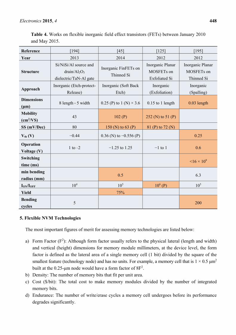
4.3. Inorganic Transistors on Flexible Silicon
Table 4 highlights works on flexible inorganic FETs. Two types of inorganic flexible
CMOS transistors on Si have been reported: traditional planar metal oxide semiconductor FET
(MOSFET) [125,194,195] and 3-dimentional out-of-plane architectural Fin-FET [45]. The electrical
and mechanical reliability aspects of the flexed transistor gate stacks, made up of a high-dielectric
constant (κ); ALD Al2O3, has also been reported and shows a lifetime degradation from electrical
stress when the stacks are flexed [196]. The degradation is attributed to increased interfacial charges,
leading to a 20% decrease in the safe operational voltage, which would satisfy the ten-year projected
lifetime industry standard. A further mechanical reliability assessment was done by observing the
effect of mechanical stress on the breakdown voltages of the devices [197]. The results showed that (i)
the breakdown voltage increased with more severe bending (lower bending radius/higher strain and
stress); (ii) constant mechanical stress might have the same effect as constant electrical stress, and,
most notably; (iii) the most severe degradation occurred in devices under dynamically varying
mechanical stress (limited number of bending cycles ~100). Otherwise, functionality was reported to
pass 200 bending cycles for planar MOSFETs [195], as reliability studies impose harder stress
conditions than a device would normally experience for accelerated tests. The minimum bending radii
increased considerably to 0.5 mm [45], while the SS, operation voltages, and most importantly,
minimum features (tens of the nanometer scale [195]) scaled down. Peak reported mobility of
252 cm2/V.s was reported by Zhai et al., in 2012 [125].
To conclude, the CMOS based flexible transistors are promising candidates for future flexible IoT
devices because of their monolithic integration ability, superior electronic properties inherent from
bulk form, and almost uncompromised reliability. However, the assessed degradation in performance
and safe operation voltages should be accounted for when designing flexible electronic systems
utilizing the flexible devices. Another important milestone to achieve fully flexible electronic systems
and devices for IoT applications is demonstrating suitable flexible NVMs that can be co-integrated
with the flexible transistors for memory storage, without compromising integration density, system
speed, and reliability.
Electronics 2015, 4 448
Table 4. Works on flexible inorganic field effect transistors (FETs) between January 2010
and May 2015.
Reference [194] [45] [125] [195]
Year 2013 2014 2012 2012
Structure
Si/NiSi/Al source and
drain/Al2O3
dielectric/TaN-Al gate
Inorganic FinFETs on
Thinned Si
Inorganic Planar
MOSFETs on
Exfoliated Si
Inorganic Planar
MOSFETs on
Thinned Si
Approach Inorganic (Etch-protect-
Release)
Inorganic (Soft Back
Etch)
Inorganic
(Exfoliation)
Inorganic
(Spalling)
Dimensions
(μm) 8 length × 5 width 0.25 (P) to 1 (N) × 3.6 0.15 to 1 length 0.03 length
Mobility
(cm2/VS) 43 102 (P) 252 (N) to 51 (P)
SS (mV/Dec) 80 150 (N) to 63 (P) 81 (P) to 72 (N)
Vth (V) −0.44 0.36 (N) to −0.556 (P) 0.25
Operation
Voltage (V) 1 to −2 −1.25 to 1.25 −1 to 1 0.6
Switching
time (ms) <16 × 109
min bending
radius (mm) 0.5
6.3
ION/IOFF 104 105 106 (P) 105
Yield 75%
Bending
cycles 5
200
5. Flexible NVM Technologies
The most important figures of merit for assessing memory technologies are listed below:
a) Form Factor (F2): Although form factor usually refers to the physical lateral (length and width)
and vertical (height) dimensions for memory module millimeters, at the device level, the form
factor is defined as the lateral area of a single memory cell (1 bit) divided by the square of the
smallest feature (technology node) and has no units. For example, a memory cell that is 1 × 0.5 μm2
built at the 0.25-μm node would have a form factor of 8F2.
b) Density: The number of memory bits that fit per unit area.
c) Cost ($/bit): The total cost to make memory modules divided by the number of integrated
memory bits.
d) Endurance: The number of write/erase cycles a memory cell undergoes before its performance
degrades significantly.

Electronics 2015, 4 449
e) Retention: The retaining ability of a memory cell to store uncompromised information over
time.
f) Operation voltage: The maximum voltage required for a write/erase operation of a memory bit.
g) Speed: The amount of time the memory cell needs to switch between different memory states
(‘0’ or ‘1’).
h) Memory window: Measures the distinguishability of the different memory states. Voltage-
sensitive memory is proportional to the voltage shift, while current sensitive memory is
proportional to the current ratio for different states.
The lower form factor means that memory cells can be arranged efficiently, resulting in reasonable
dimensions for the memory array. The higher the integration density, the more bits can be integrated
on a specific real estate substrate area (i.e., smaller dies) and the lower the overall bit/cost. Higher
endurance is desirable for multiple writing and erasing of data from memory cells and a retention of
ten years is the benchmark industry standard for NVMs. Lower operation voltage and high speeds
translate into lower power consumption because the switching time when maximum power is drawn is
lower as well as the supplied voltage, a sizeable concern for portable and battery operated systems.
Furthermore, fast switching means that the NVM can support a faster execution of instructions during
processing and computations. The larger the memory window, the more lenient the requirements on
the sense circuitry needed to differentiate whether the stored bit is a ‘0’ or a ‘1’.
5.1. Flexible ReRAM
ReRAM or memristors are passive circuit elements that can have two resistance values: high and
low resistance states. They act as NVM elements by sensing their resistance during a read cycles or
switching their resistance state during write cycles. Memristors were conceptualized by Leon Chua in
1971 [146] and first experimentally demonstrated in 2008 by a team led by R. Stanley Williams at
Hewlett Packard labs in 2008 [145]. Since then, memristors have grabbed the attention of the scientific
community due to their simplistic structure, fast switching, and possible applications for neuromorphic
computations. In 2010, S. Jo et al. experimentally demonstrated that CMOS neurons and memristor
synapses in a crossbar configuration can support synaptic functions [144]. Extensive research on
memristors led to the report of 10 nm × 10 nm ReRAMs at the in International Electron Device
Meeting (IEDM) in 2011 [143]. These dimensions were targeted for flash by 2020, based on the ITRS
report of 2011 [198]. Memristors are usually integrated in a very dense architecture of cross bars.
Furthermore, there are some proposed techniques for using memristor single cells in memory arrays
without access/select transistors and for avoiding sneak paths by using a multiple reading sequence [199].
Besides the common perks of flexible electronics, and hence memories, ranging from portable,
lightweight, stylish designs, and conformal ability consumer electronics to biomedical applications,
flexible memristors would not only support these functionalities but also provide a feasible route for
mimicking our brain’s cortex structure. Key works on flexible memristors can be classified into four
main categories: organic memristors on organic substrates [81,86,87,200–205], inorganic resistive
memories on silicon transferred to organic substrates [27,206], inorganic memristors deposited at low
temperatures on plastic organic substrates [78,207–217], and inorganic memristors on flexed silicon

Electronics 2015, 4 450
using the etch-protect-release approach [218]. In addition, interesting work using inorganic flexible
substrate (Al foil) with organic cellulose nanofiber paper enabled achieving the lowest reported
bending radius for ReRAM (0.35 mm) and lowest operating voltage (±0.5 V) [219]. Table 5
summarizes the key works on flexible ReRAM over the past five years.
5.2. Flexible FeRAM
In general, FeRAMs have superior endurance and low variability which represent critical challenges
for state-of-the-art redox memristive memories [220]. The two common FeRAM memory architectures
using access transistors and ferroelectric capacitors are the 1T-1C, which consists of one transistor and
one capacitor per memory cell and 2T-2C, which consists of two transistors and two capacitors for
each memory cell [221]. Ferroelectric materials have bi-stable polarization states that can provide
useful information for NVM applications, with one state corresponding to a ‘1’ and the other to a ‘0’.
Hence, they are used in simple metal/ferroelectric/metal structures to make highly scalable
ferroelectric capacitors, suitable for ultra-high density integration. Rigid ferroelectric random access
memories (FeRAM) have already made a great leap by their introduction to the market; hence, it is a
relatively mature technology compared to other emerging NVM technologies. FeRAMs are
commercially available in Texas Instruments’ microprocessors and Fujitsu’s RF tags [222–224]. The
commonly used ferroelectric material in FeRAM is lead zirconium titanate (Pb1.1Zr0.48Ti0.52O3—PZT)
due to its high switching speed [225,226], low cost per bit ($/bit), and low operation voltage [227,228].
Hence, the best properties for flexible NVM FeRAM are reported for structures incorporating PZT as
the ferroelectric material, as evident from Table 6. However, PZT-based flexible FeRAM was not
achievable on organic platforms because of PZT’s high crystallization temperature (>600 °C), well
above the melting temperature of most polymeric organic substrates. Hence, PZT FeRAMs have been
demonstrated only on flexible silicon and platinum foil [229,230] or built on silicon and then
transferred to polymeric flexible substrates [84,231]. Nevertheless, the highest level of mechanical
durability (20,000 bending cycles) has been reported for hybrid FeRAMs with inorganic devices
transferred to a polymeric substrate [232,233]. Further studies have been conducted on PZT-flexible
FeRAM under the combined effect of high temperature (225 °C) and bending condition (1.25 cm
bending radius—corresponding to 0.16% nominal strain and ~260 MPa pressure) [234]. These
researchers showed evidence of a trend for degradation at higher temperatures but also that
temperatures did not affect the retention or the endurance/fatigue properties; however, the memory
window (defined as the ratio between switching and nonswitching currents) was significantly reduced
at higher temperatures. Interestingly, by capitalizing on standard industry processing techniques, the
flexible PZT ferroelectric NVM has the potential to achieve properties similar to those of the best
available bulk devices; these are summarized in Table 7.

Electronics 2015, 4 451
Table 5. Summary of the key works on flexible resistive random access memory (ReRAM) over the past five years.
Reference [205] [217] [212] [204] [206] [211] [210]
Year 2010 2012 2013 2012 2014 2015 2012
Memory Type (1R) (1R) (1T) (1R) (1D1R) (1R) (1R)
Flexible Final
Structure
PET/Ti/Au/Al/P
I:PCBM/Al PEN/Au/Ag2Se/Ag
PI/SiO2/Ti source and
drain/a-IGZO/Ni gate
PEN/Al
bottom/coPI
layer/ Al top
PI/Si-p-n types
diode/Cu/CuOx/Al
PET/ITO/
WO3.H2O
nanosheets/Cu
Glass/graphene/SiOx/
Graphene
Approach All organic
Hybrid (low
temperature
deposition)
Hybrid (Deposition at
Low Temperature) All organic
Hybrid (Transfer +
Low Temperature
Deposition)
Hybrid (Low
Temperature
Deposition)
Hybrid (Low
Temperature
Deposition)
Operating Voltage (V) 4.5 −2 −0.5 to +2 −3 +2 and +5 −1.4 to +1 0 to +14
Form Factor (F2) -- -- 2 -- 11.1 -- --
Memory Window (V) -- -- 1 -- 1 -- --
Speed (ns) -- 500 × 103 1000 5 × 10⁶ -- 50
Endurance (cycles) 50 104 106 104 100 5000 400
Retention (s) 104 105 104 104 105 105 5 × 10⁴
Operating
temperature (°C) 25 200 85 25 25 25 25
Bending Radius (mm) 9 16 10 5 10 8 6
Bending Cycles 140 100 1000 1000 1000 2000 300
Yield -- -- -- 95%–99% 85%–90% -- 70%
Cell Dimensions (µm) -- -- 10 × 20 channel 200 × 200 150 × 300 channel
-- 100 diameter 600 × 600 500 cell

Electronics 2015, 4 452
Table 5. Cont.
Reference [87] [27] [203] [86] [209] [208]
Year 2010 2011 2010 2010 2012 2014
Memory Type (1R) (1T1R) (1R) (1R) (1R) (1R)
Flexible Final
Structure PES/Al/graphene-O/Al
Plastic/transferred Si channel
material/Au source and drain-> on
drainAl/TiO2/Al + Au for
WL,BL, and SL
PET/ITO/PMMA/
graphene/PMMA/Al
PET/ITO/
graphene-O/Al PES/Al/ZrO2/Al Kapton/Cu/CuOx/Ag
Approach All organic Hybrid (Transfer) All organic All organic
Hybrid (Low
Temperature
Deposition)
Hybrid (Low
Temperature
Deposition)
Operating Voltage
(V) −4 −4 to +10 −5 −2 to +3 −0.5 to 2.8 −1 to +1
Form Factor (F2) -- 20 -- -- -- --
Memory Window (V) -- 4 -- -- -- --
Speed (ns) -- -- 106 -- -- --
Endurance (cycles) 100 100 1.5 × 10⁵ 100 778 100
Retention (s) 105 104 105 5 × 10⁶ 105 120 × 104
Operating
temperature (°C) 25 25 25 25 25 −18 to 82
Bending Radius (mm) 7 5 10 4 -- 5
Bending Cycles 1000 1000 -- 1000 -- 1000
Yield 80% 60% -- -- -- --
Cell Dimensions (µm) 50 × 50 10 × 200 17.74 to 26.71 diameter -- -- 20 × 20

Electronics 2015, 4 453
Table 5. Cont.
Reference [207] [219] [78] [218] [81] [202] [201]
Year 2012 2014 2015 2014 2012 2014 2015
Memory Type (1R) (1R) (1R) (1R) (1D-1R) (1R) (1R)
Flexible Final
Structure PES/Cu/TiO2/Cu
Al foil/Ag-CNP(cellulose
nanofiber paper)/Ag
PET/Au/Black
Phosphorous Quant
Dots (BPQD)-PVP/Ag
Si/SiO2/Al/TaN/
Al2O3/TaN/Al
PI/Al/B-CNT
and N-CNT in
polystyrene/Al
PET/rGo/g-
C3N4-NSs/rGo
Au/HKUST-
1/Au/PET
Approach Hybrid (Deposition at
Low Temperature)
Hybrid (Inorganic Flexible
Substrate + Organic Device)
Hybrid (Deposition at
Low Temperature) Inorganic All Organic All Organic All Organic
Operating Voltage (V) 0 to 1.5 −0.5 −1.2 to +2.8 −11 to +11 3 4.87 0.78
Form Factor (F2) -- -- -- -- -- -- --
Memory Window (V) -- -- -- -- -- -- --
Speed (ns) -- -- -- -- -- -- --
Endurance (cycles) -- 100 -- -- 100 50 106
Retention (s) -- 105 1.1 × 10³ -- 105 5000 104
Operating
temperature (°C) -- 25 25 25 25 25 −70 to +70
Bending Radius (mm) 10 0.35 -- 1 10 8 3.2
Bending Cycles 100 1000 -- -- 500 1000 160
Yield -- -- -- -- -- -- --
Cell Dimensions (µm) -- 50 × 50
500 × 500 100 × 100 --
1000 × 3000 100
diameter 500 × 500 250 × 250

Electronics 2015, 4 454
Table 6. Summary of the key works on flexible ferroelectric random access memories (FeRAM) over the past five years.
Reference [84] [231] [235] [232] [233] [236] [229]
Year 2013 2010 2012 2011 2011 2013 2015
Memory Type Ferroelectric (1T) Ferroelectric
(1C)
Ferroelectric
(1C) Ferroelectric (1T) Ferroelectric (1T) Ferroelectric (1C)
Ferroelectric
(1C)
Flexible Final
Structure
PI/Su-8/SiO2/Pt gate
electrode/
PZT/graphene
channel/ Cr-Au for
source and drain
electrodes
Plastic/Cr-
Au/Ti-
Pt/PZT/Pt/Cr/Au
Al foil/
PVD-TrFE/
Au
PEN/Ti-Au-Ti soucre and
drain/Al2O3/ZnO
channel/Al2O3 interface
dielectric/PVDF-TrFE
ferroelectric/Au
Au/poly(vinylidene fluoride-
trifluoroethylene)/Al2O3/ZnO/Ti/Au/Ti/
poly(ethylene naphthalate)
ULTEM
1000B/PEDOT:PSS/P(VDF-
TrFE)/PEDOT:PSS
Si/SiO2/Ti-
Pt/PZT/Pt
Approach Hybrid (Transfer) Hybrid
(Transfer)
Hybrid
(Transfer)
Hybrid (Low Temperature
Deposition) Hybrid (Low Temperature Deposition) All organic (ink-jet printing) Inorganic
Operating Voltage (V) −11 −3 −12 −14 to +12 −10 to +8 −30 −15
Form Factor (F2) 8 -- -- 2 2 -- --
Memory Window (V) 6 -- -- 7.8 3.4 -- --
Speed (ns) -- -- -- 1 × 10⁹ 2 × 10⁹ 50 × 106 500
Endurance (cycles) 1000 -- -- -- -- 45% polarization after 105 109
Retention (s) 200 -- -- 1.5 × 10⁴ <104 -- 105
Operating temperature
(°C) 25 25 25 25 25 25 200
Bending Radius (mm) 9 8 6 9.7 9.7 -- 5
Bending Cycles 200 -- 500 2 × 10⁴ 2 × 10⁴ -- 1000
Yield -- -- -- -- -- -- 95%
Cell Dimensions (µm ) 10 × 80 channel 100 × 400 180
diameter 20 × 40 channel 20 × 40 channel 60 × 60
100 × 100
250 × 250

Electronics 2015, 4 455
Table 6. Cont.
Reference [237] [238] [239] [240] [230] [241] [242] [243]
Year 2011 2011 2012 2012 2012 2015 2014 2013
Memory Type Ferroelectric (1C) Ferroelectric (1C) Ferroelectric (1T) Ferroelectric (1C) Ferroelectric
(1C)
Ferroelectric
(1R) Ferroelectric (1T) Ferroelectric (1T)
Flexible Final
Structure
PEN/PEDOT:PSS/P(VDF-
TrFE)/PEDOT:PSS
PEN/Au/P(VDF-
TrFE)/Au
Bank
Note/PDMS/PEDOT:PSS
bottom electrode/ P(VDF-
TrFE) ferroelectric/
Pentacene channel/ Au
soucre and drain
Ag/BaTiO3/PVDF-
TrFE
nanocomposites/Ag
Pt/PZT
(200 nm)/SRO
(30 nm)/Pt
(200 nm) foil
PET/Ag
ink/PVDF-
TrFE/Ag ink
PDMS/Au source and
drain/F8T2 organic
semiconductor/PVDF-
TrFE ferroelectric/ Al
gate
PI/PVP/Au source
and Drain/Polymer
blend
channel/PVDF-TrFE
ferroelectric/Al gate
Approach All organic All organic All organic
Hybrid
(inorganic/organic
composite substrate
and device)
Inorganic All Organic All Organic All Organic
Operating Voltage (V) −10 −30 to +30 −15 to +15 −3.3 −4 23 −20 to +20 −80 to +80
Form Factor (F2) -- -- 16.67 -- -- -- 3 1
Memory Window (V) -- -- 8 -- -- -- 11 35
Speed (ns) 106 10 × 103 -- -- -- 108 108 --
Endurance (cycles) 106 has 80% Pr -- 105 -- 107 -- 6 × 10⁴ 100
Retention (s) -- -- 104 -- -- -- 2000 104
Operating temperature
(°C) 25 25 25 25 25 25 25 25
Bending Radius (mm) -- 6.5 -- -- -- -- 6 --
Bending Cycles -- -- -- -- -- -- -- --
Yield -- -- 90% -- -- -- -- --
Cell Dimensions (µm ) -- 25 × 25
60 × 1000 channel -- 100 diameter 30 × 30 20 × 60 20 × 20 50 × 50

Electronics 2015, 4 456
Table 7. Summary of best reported values for PZT- based ferroelectric nonvolatile
memory (NVM).
Property Best Reported Value for PZT-based FeRAM
Switching Speed Pico seconds regime for material switching [225,226] and 70 ns for actual
arrays due to bit/word line capacitances [244]
Ferroelectric Capacitor’s
Lateral Dimensions
0.1 µm2 [245]
Switching Energy 400 fJ/bit [246]
Retention >10 years @ 85 °C [247] , experimentally three days (2.5 × 10^5) was
demonstrated for FeRAM (using SrBi2Ta2O9(SBT)) [248,249]
Technology Node (CMOS
Logic)
130 nm [247]
Operation Voltage 1.5 Volts [246]
Read/Write Cycles >1015 [250,251]
5.3. Flexible PCRAM
Phase change materials exhibit high resistance in the highly disordered amorphous phase and low
resistance in the highly ordered crystalline phase, where each resistance state corresponds to a ‘0’ or a
‘1’. The transition to the amorphous phase requires applying high temperatures above the melting point
of the phase change material for a brief time, while the transition to the crystalline phase requires
lower temperatures for a longer duration to supply the required energy for re-organizing the material
structure. PCRAM is generally characterized by high switching transition speeds. In 2010, Hong et al.
reported a flexible version of the Ge2Sb2Te5-based PCRAM on polyimide that required a 30 ns pulse to
switch [252]. Another advantage of PCRAM is its highly localized regions of phase change that
enables ultra-high integration densities. In 2011, Hong et al. also reported phase-change nano-pillar
devices with the potential of reaching up to tera bit/squared inch densities on flexible substrates [253]
and the following year, Yoon et al. demonstrated a 176 Gbit/square inch PCRAM [254], the highest
reported density on a flexible substrate. The highest reported bending cycles endurance (1000 bending
cycles) and yield (66%) for flexible PCRAM was reported by Mun et al., in 2015 [255]. Table 8
summarizes the work on flexible PCRAM undertaken over the past five years.

Electronics 2015, 4 457
Table 8. Summary of the key works on flexible PCRAM over the past five years.
Reference [252] [253] [254] [255]
Year 2010 2011 2012 2015
Memory Type PCRAM (1R) PCRAM (1R) PCRAM (1R) PCRAM (1D-1R)
Flexible Final
Structure PI/TiN/GST/Pt probe tip
PET or PI or Stainless steel/ TiW bottom
electrode/GST (Ge2Sb2Te5)/Cr top electrode
GFR Hybrimer Film/TiN/Pt/TiN/IST/Ps-
b-PMMA/Cr
BCP/Transferred Si Diode/TiW
bottom electrode/GST/SiOx
cylinders/TiN/TiW top electrode
Approach
Hybrid (Low Temperature Deposition
+ Transfer by Hot Embossing and
Nano Imprint Lithography -NIL)
Hybrid (Low Temperature Deposition + NIL) Hybrid (Low Temperature Deposition) Hybrid (transfer + low temperature
deposition)
Operating
Voltage (V) 1.8 3 1.8 8.5
Form Factor (F2) -- -- -- --
Memory
Window -- -- -- --
Speed (ns) 30 200 100 1000
Endurance
(cycles) -- -- -- 100
Retention (s) -- -- -- 104
Operating
temperature (°C) 25 25 25 25
Bending Radius
(mm) -- -- 2.25 10
Bending Cycles -- -- -- 1000
Yield -- -- -- 66%
Cell Dimensions
(μm) 0.2 to 0.3 diameter 0.25 diameter 0.035 diameter --
Electronics 2015, 4 458
5.4. Flexible Flash
Flash memories are the most mature NVM technology in today’s market. Flash memories have the
same FET structure with an extra embedded layer for charge trapping/storage for simple
nondestructive readout operations [75,256]. The charge-trapping layer is sandwiched between two
dielectrics. The first dielectric is a blocking oxide, which is a thick oxide to prevent charge transfer
between the control gate and the charge-trapping layer. The second is a tunneling oxide with
thicknesses varying between 7 and 10 nm through which charge transfer takes place between the FET
channel and the charge-trapping layer. The two aforementioned flash types, the CT-flash and the
FG-flash, differ in the nature of the charge-trapping layer used. FG-flash has a floating conductor/gate
previously made of doped polysilicon that has recently been shifting to conductive NPs and QDs for
charge trapping. CT-flash has an insulating charge-trapping layer. Building on the structural
difference, there is also a fundamental difference in the physical operation. The stored charge is
removed/erased from a FG-flash memory through Fowler-Nordheim (FN) tunneling between the
charge-trapping layer and the FET channel, where a strong electric field is applied at the gate reducing
the effective tunneling barrier width [257]; whereas, in hot-hole injection, where an electric field
causes a hole with sufficient energy in the channel to tunnel, neutralizing a stored charge in the
charge-trapping layer [258], which serves as the erasing mechanism in CT-flash. Both FG-flash and
CT-flash are programmed using hot electron injection from the channel to the charge-trapping layer.
Compared to FN tunneling, hot carrier injection requires lower electric fields, which allowed for the
scaling down of the tunneling oxide thickness without compromising its reliability [70,73,74,256,259].
To overcome the challenges associated with traditional FG-flashes, NPs and nanocrystal FG-flashes
have recently been introduced.
Despite the widespread adoption of flash memories in a myriad of applications, the status quo for
flexible flash memories does not reflect the perks of the long commercialized rigid flash. This is in part
due to the focus on replacing the semiconductor’s standard processes and materials in favor of flexible
new materials and low-temperature processes. Limited by the organic material choices of the
all-organic approach and low-temperature depositions of the hybrid approach to flexible NVMs,
current flexible flash memories have reported operation voltages ranging from ±5 to ±90 V [77,260]
with minimum channel length dimensions of 2-μm [80]. Nonetheless, good bendability has been
achieved up to 5 mm [85,261] for 2000 bending cycles [77], an endurance of 100,000 cycles [76], and
a retention ability of 106 s [73]. Table 9 summarizes the work done on flexible flash NVMs since 2010.
To summarize, due to the various approaches towards achieving flexible electronics, the versatility
of nonvolatile memory technologies, and relative infancy of emerging NVM technologies, flexible
NVM elements face more challenges in order to match their bulk counterparts. For instance, cellulose
nanofiber ReRAM on Al foil achieved ±0.5 V operation voltage but integration ability with CMOS
technology is a challenge. FeRAM being relatively a mature technology and since its transformation
from bulk to flexible form in a CMOS compatible process has been demonstrated, holds potential for
suitability for IoT applications. Based on the possible optimizations in Table 7, the flexible FeRAM
using the inorganic approach can potentially achieve low power operation, high endurance, 10 years
retention, and the ability to be integrated in 130 nm CMOS technology. However, the demonstrating
this potential has not been reported. Although a flexible 176 Gb/square inch has been demonstrated, it

Electronics 2015, 4 459
suffers from low yield. This is a critical challenge when discussing application in IoT and big data
analysis where gigantic memory arrays are to be utilized because faulty memory bit provides wrong
information and can have a detrimental effect on neighboring memory cells in the array. Flexible flash
NVMs are far from state-of-the-art bulk flash properties because most of the research done focused on
new material systems and processes.
In the IoT era, where smart electronic devices are able to make decisions autonomously without
human intervention for application in fully automated cars that car drive itself at high speeds the
integrity of electronic systems and its ability to store and process large pieces of information in a
fractions of a second cannot be compromised. CMOS based electronics have demonstrated great
integrity, as well as fast and reliable performance for decades through the well-established and heavily
invested infrastructures and standard processes. Although the fact that a flexible version of
state-of-the-art CMOS transistors has been demonstrated holds promise for flexible electronics,
flexible NVMs are still the weaker link in the chain and without NVMs, fully flexible electronic
systems cannot be achieved.
6. Conclusions and Future Prospects
Exciting progress has been made in flexible electronics research over the past few decades. OLED
flexible screens are already available in the market, and numerous novel biomedical and wearable
applications using flexible electronics have been proposed. At this stage, expectations for silicon-based
electronics are high and the status quo is for high performance, fast, low power, compact, and reliable
aspects, some of which might not cross the chasm to the flexible arena. This is the core value for which
the research field of transfer-free inorganic silicon-based flexible electronics is created. However, this
approach is relatively new compared to the ongoing research on flexible organic electronics, where
organic materials are used as substrates or device material.
In this review, we have presented a brief overview of flexible electronics research, focusing on
NVM components. We listed the mainstream NVM architectures and technologies with a special focus
on flexible devices and provided benchmarking tables for transistors and storage devices derived from
the three main approaches: (1) all organic; (2) hybrid; and (3) inorganic.
Future prospects indicate that a number of challenges will have to be overcome before flexible
ReRAM, FeRAM, PCRAM, MRAM, and flash will be primed for commercialization. Flexible
FeRAM has an edge because of its rigid current form that is used as an embedded NVM in
microprocessors. Flash has the highest potential owing to the maturity of the technology in the rigid
state; furthermore, the transfer of this technology and progress to the flexible arena will definitely
speed up the introduction of commercial flexible flash NVM for various applications. On the other
hand, ReRAM, PCRAM, and MRAM are still emerging technologies, even in their bulk rigid form.
The potential for extreme scaling, fast speeds, and low-power operation of NVMs is attracting the
attention of both researchers and industry such that they might catch up with competing mature
technology in the flexible arena earlier than expected.

Electronics 2015, 4 460
Table 9. Summary of the key works on flexible Flash memory over the past five years.
Reference [260] [82] [80] [76] [77]
Year 2012 2011 2012 2014 2011
Memory Type Flash + Nano Particles (1T) Flash (1T) Flash (1T) Flash (1T) Flash (1T)
Flexible Final Structure
PET/Ag gate
electrode/Al2O3/PMMA with
Au NP composite/Pentacene/Au
source and drain electrodes
PET/graphene gate
electrode/Al2O3/CNT
channel/graphene for source
and drain electrodes
PES/Si NW/Al2O3/Pt-
NP//Al2O3/Al source,
drain, and gate
PET/ P(NDI2OD-T2) Channel/ Au
source and drain/PVA tunneling
dielectric/ Au-NP/
P(VDF−TrFE−CFE) blocking
dielectric/ Al gate
PES/ITO gate/PVP
blocking/APTES-Au-NP/PVP
tunneling/MoO3 buffer/ Pentacene
channel/ITO source and drain
Approach All organic All organic Hybrid (Transfer) All organic All organic
Operating Voltage (V) −5 to +5 −10 to +10 −10 to +10 −6 to +6 −90 to +90
Form Factor (F2) 10 -- -- 20 10
Memory Window 2.1 10 1.85 2 15
Speed (ns) -- 100 107 2 × 10⁹ 1 × 10⁹
Endurance (cycles) 1000 500 104 105 --
Retention (s) 105 1000 104 105 105
Operating temperature (°C) 100 25 25 25 85
Bending Radius (mm) 10 8 16 9 20
Bending Cycles 1000 1000 1000 100 2000
Yield -- -- -- -- --
Cell Dimensions (μm) 50 × 500 channel -- 2 channel length 100 × 2000 channel 100 × 1000 channel

Electronics 2015, 4 461
Table 9. Cont.
Reference [262] [74] [85] [73] [261]
Year 2012 2010 2012 2013 2015
Memory Type Flash (1T) Flash (1T) Flash (1T) Flash (1T) Flash (1T)
Flexible Final
Structure
PES/Al source and
drain/ZnOPDA/AlOx-
SAOLs/Zno:Cu/AlOx-
SAOLs/Pentacene/ Al gate
PES/Ti-Au gate/ PVP blocking/ APTES-Au
NP storage/PVP tunneling/ Pentacene channel/
Au source and drain
PEN/graphene
channel/Al2O3/HfOx/Al2O3/ ITO
PET/ITO gate/Al2O3/Au NP
charge trapping/Al2O3/PDPP-
TBT/Au source and drain
PDMS/PI/Au/Al2O3-
SiO2/SWCNT/Au
Approach Hybrid (Low Temperature
Deposition) All organic
Hybrid (Deposition at Low
Temperature) All organic Hybrid (Transfer)
Operating Voltage (V) −15 to +15 −90 to +90 −21 to +23 −40 to +40 −25 to +25
Form Factor (F2) 2 10 6.67 20 11
Memory Window 14.1 9.7 8.6 7.5 13.2
Speed (ns) 1 × 10⁸ 1 × 10⁹ hypothesized ~14 ns read time and
20 μs/20 ms write/erase time 10 × 107 105
Endurance (cycles) -- 700 -- 1000 104
Retention (s) 1000 105 30% after 10 years 106 104
Operating
temperature (°C) 25 25 degrades at 85 25 25
Bending Radius (mm) -- 20 5 10 5
Bending Cycles -- 1000 10 1000 1000
Yield -- -- -- -- --
Cell Dimensions (μm) 50 × 100 channel 100 × 1000 channel 30 × 4.5 channel 50 × 1000 channel 18 × 200

Electronics 2015, 4 462
These novel flexible NVM technologies along with the required flexible transistors for array gating
and data processing are enabling technologies for the foreseen future where a galactic network of
connected devices can autonomously detect, collect, and process surrounding information to make real
time decisions fulfilling the IoT futuristic vision. The NVMs will store instructions and data in both
power-on and power off states consuming minimal power. Furthermore, to meet the ultra-low power
requirements for IoT devices when the collected information does not need real time processing,
integrating ultra-high density NVMs will help store large amount of information to be analyzed when
the device is externally charging, instead of sending data continuously through an antenna and
consuming extra power. This is useful when collecting activity level throughout the day, similar to the
study conducted by Hitachi that provided a link between variability of motion and happiness. NVMs
will also have to cope with ultra-large scale integration to be able to store the huge amounts of
information for big data analysis, in compact ultra-mobile devices, that can be preferably
monolithically integrated in state-of-the-art CMOS technologies to expedite its introduction in the
consumer electronics market. However, the status quo of flexible NVMs shows that there is still a gap
between current bulk devices’ properties and their flexible counterparts. Hence, flexible NVMs and
flexible electronic systems are still hindered from invading the consumer electronics market and still
provide less attractive alternative to replacing bulk devices for future IoT applications. The core
challenge is to either invent new technologies that can rival CMOS integration ability and standard
processes at a reasonable cost, or to embrace CMOS technology in making flexible devices while
obtaining flexibility as an extra feature without affecting critical performance metrics of the devices.
Acknowledgments
We acknowledge the KAUST OCRF CRG-1 grant CRG-1-2012-HUS-008 to MTG. We also thank
Carolyn Unck, Editor, Academic Writing of KAUST for proof reading and editing our manuscript.
Conflicts of Interest
The authors declare no competing financial interest. We have also diligently secured copyrights for
already published materials used in this review paper.
References
1. Zhou, H.; Seo, J.-H.; Paskiewicz, D.M.; Zhu, Y.; Celler, G.K.; Voyles, P.M.; Zhou, W.;
Lagally, M.G.; Ma, Z. Fast flexible electronics with strained silicon nanomembranes. Sci. Rep.
2013, 3, 1291.
2. Des Etangs-Levallois, A.L.; Lesecq, M.; Danneville, F.; Tagro, Y.; Lepilliet, S.; Hoel, V.;
Troadec, D.; Gloria, D.; Raynaud, C.; Dubois, E. Radio-frequency and low noise characteristics
of SOI technology on plastic for flexible electronics. Solid-State Electron. 2013, 90, 73–78.
3. Nasr, B.; Wang, D.; Kruk, R.; Rösner, H.; Hahn, H.; Dasgupta, S. Flexible Electronics:
High‐Speed, Low‐Voltage, and Environmentally Stable Operation of Electrochemically Gated
Zinc Oxide Nanowire Field‐Effect Transistors. Adv. Funct. Mater. 2013, 23, 1729–1729.

Electronics 2015, 4 463
4. Han, S.T.; Zhou, Y.; Wang, C.; He, L.; Zhang, W.; Roy, V. Flexible Electronics: Layer‐by‐Layer‐Assembled Reduced Graphene Oxide/Gold Nanoparticle Hybrid Double‐Floating‐Gate
Structure for Low‐Voltage Flexible Flash Memory. Adv. Mater. 2013, 25, 793–793.
5. Farsinezhad, S.; Mohammadpour, A.; Dalrymple, A.N.; Geisinger, J.; Kar, P.; Brett, M.J.;
Shankar, K. Transparent anodic TiO2 nanotube arrays on plastic substrates for disposable
biosensors and flexible electronics. J. Nanosci. Nanotechnol. 2013, 13, 2885–2891.
6. Majewski, L.; Grell, M.; Ogier, S.; Veres, J. A novel gate insulator for flexible electronics. Org.
Electron. 2003, 4, 27–32.
7. McAlpine, M.C.; Friedman, R.S.; Lieber, C.M. High-performance nanowire electronics and
photonics and nanoscale patterning on flexible plastic substrates. Proc. IEEE 2005, 93,
1357–1363.
8. Sun, Y.; Rogers, J.A. Inorganic semiconductors for flexible electronics. Adv. Mater. 2007, 19,
1897–1916.
9. Rogers, J.A.; Someya, T.; Huang, Y. Materials and Mechanics for Stretchable Electronics.
Science 2010, 327, 1603–1607.
10. Sokolov, A.N.; Tee, B.C.K.; Bettinger, C.J.; Tok, J.B.H.; Bao, Z. Chemical and Engineering
Approaches To Enable Organic Field-Effect Transistors for Electronic Skin Applications. Acc.
Chem. Res. 2012, 45, 361–371.
11. Wang, C.; Hwang, D.; Yu, Z.; Takei, K.; Park, J.; Chen, T.; Ma, B.; Javey, A. User-interactive
electronic skin for instantaneous pressure visualization. Nat. Mater. 2013, 12, 899–904.
12. Mei, Y.; Loth, M.A.; Payne, M.; Zhang, W.; Smith, J.; Day, C.S.; Parkin, S.R.; Heeney, M.;
McCulloch, I.; Anthopoulos, T.D. High Mobility Field‐Effect Transistors with Versatile
Processing from a Small‐Molecule Organic Semiconductor. Adv. Mater. 2013, 25, 4352–4357.
13. Kim, R.H.; Kim, H.J.; Bae, I.; Hwang, S.K.; Velusamy, D.B.; Cho, S.M.; Takaishi, K.; Muto, T.;
Hashizume, D.; Uchiyama, M. Non-volatile organic memory with sub-millimetre bending radius.
Nat. Commun. 2014, 5, 3583.
14. Liu, X.; Guo, Y.; Ma, Y.; Chen, H.; Mao, Z.; Wang, H.; Yu, G.; Liu, Y. Organic Electronics:
Flexible, Low‐Voltage and High‐Performance Polymer Thin‐Film Transistors and Their
Application in Photo/Thermal Detectors . Adv. Mater. 2014, 26, 3569.
15. Lai, Y.-C.; Huang, Y.-C.; Lin, T.-Y.; Wang, Y.-X.; Chang, C.-Y.; Li, Y.; Lin, T.-Y.; Ye, B.-W.;
Hsieh, Y.-P.; Su, W.-F. Stretchable organic memory: Toward learnable and digitized stretchable
electronic applications. NPG Asia Mater. 2014, 6, e87.
16. Tiwari, J.N.; Meena, J.S.; Wu, C.S.; Tiwari, R.N.; Chu, M.C.; Chang, F.C.; Ko, F.H. Thin‐Film
Composite Materials as a Dielectric Layer for Flexible Metal–Insulator–Metal Capacitors.
ChemSusChem 2010, 3, 1051–1056.
17. Kraft, U.; Sejfić, M.; Kang, M.J.; Takimiya, K.; Zaki, T.; Letzkus, F.; Burghartz, J.N.; Weber, E.;
Klauk, H. Flexible Low‐Voltage Organic Complementary Circuits: Finding the Optimum
Combination of Semiconductors and Monolayer Gate Dielectrics. Adv. Mater. 2015, 27,
207–214.
18. Yokota, T.; Kuribara, K.; Tokuhara, T.; Zschieschang, U.; Klauk, H.; Takimiya, K.;
Sadamitsu, Y.; Hamada, M.; Sekitani, T.; Someya, T. Flexible Low‐Voltage Organic Transistors
with High Thermal Stability at 250 °C. Adv. Mater. 2013, 25, 3639–3644.

Electronics 2015, 4 464
19. Lien, D.-H.; Kao, Z.-K.; Huang, T.-H.; Liao, Y.-C.; Lee, S.-C.; He, J.-H. All-printed paper
memory. ACS Nano 2014, 8, 7613–7619.
20. Kim, S.; Cook, B.; Le, T.; Cooper, J.; Lee, H.; Lakafosis, V.; Vyas, R.; Moro, R.; Bozzi, M.;
Georgiadis, A. Inkjet-printed antennas, sensors and circuits on paper substrate. IET Microw.
Antennas Propag. 2013, 7, 858–868.
21. Chung, S.; Jang, M.; Ji, S.B.; Im, H.; Seong, N.; Ha, J.; Kwon, S.K.; Kim, Y.H.; Yang, H.;
Hong, Y. Flexible High‐Performance All‐Inkjet‐Printed Inverters: Organo‐Compatible and Stable
Interface Engineering. Adv. Mater. 2013, 25, 4773–4777.
22. Baeg, K.J.; Caironi, M.; Noh, Y.Y. Toward printed integrated circuits based on unipolar or
ambipolar polymer semiconductors. Adv. Mater. 2013, 25, 4210–4244.
23. Carlson, A.; Bowen, A.M.; Huang, Y.; Nuzzo, R.G.; Rogers, J.A. Transfer printing techniques
for materials assembly and micro/nanodevice fabrication. Adv. Mater. 2012, 24, 5284–5318.
24. Stauth, S.A.; Parviz, B.A. Self-assembled single-crystal silicon circuits on plastic. Proc. Natl.
Acad. Sci. USA 2006, 103, 13922–13927.
25. Kim, T.-I.; Jung, Y.H.; Chung, H.-J.; Yu, K.J.; Ahmed, N.; Corcoran, C.J.; Park, J.S.; Jin, S.H.;
Rogers, J.A. Deterministic assembly of releasable single crystal silicon-metal oxide field-effect
devices formed from bulk wafers. Appl. Phys. Lett. 2013, 102, 182104.
26. Lee, C.H.; Kim, D.R.; Zheng, X. Fabricating nanowire devices on diverse substrates by simple
transfer-printing methods. Proc. Natl. Acad. Sci. USA 2010, 107, 9950–9955.
27. Kim, S.; Jeong, H.Y.; Kim, S.K.; Choi, S.-Y.; Lee, K.J. Flexible memristive memory array on
plastic substrates. Nano Lett. 2011, 11, 5438–5442.
28. Sevilla, G.A.T.; Rojas, J.P.; Fahad, H.M.; Hussain, A.M.; Ghanem, R.; Smith, C.E.; Hussain,
M.M. Flexible and Transparent Silicon‐on‐Polymer Based Sub‐20 nm Non‐planar 3D FinFET for
Brain‐Architecture Inspired Computation. Adv. Mater. 2014, 26, 2794–2799.
29. Liang, L.; Li, K.; Xiao, C.; Fan, S.; Liu, J.; Zhang, W.; Xu, W.; Tong, W.; Liao, J.; Zhou, Y.
Vacancy Associates-rich Ultrathin Nanosheets for High Performance and Flexible Nonvolatile
Memory Device. J. Am. Chem. Soc. 2015, 137, 3102–3108.
30. Zhang, L.; Wang, H.; Zhao, Y.; Guo, Y.; Hu, W.; Yu, G.; Liu, Y. Substrate‐free ultra‐flexible
organic field‐effect transistors and five‐stage ring oscillators. Adv. Mater. 2013, 25, 5455–5460.
31. Kang, B.; Lee, W.H.; Cho, K. Recent advances in organic transistor printing processes. ACS
Appl. Mater. Interfaces 2013, 5, 2302–2315.
32. Kim, S.; Son, J.H.; Lee, S.H.; You, B.K.; Park, K.I.; Lee, H.K.; Byun, M.; Lee, K.J. Flexible
Crossbar‐Structured Resistive Memory Arrays on Plastic Substrates via Inorganic‐Based Laser
Lift‐Off. Adv. Mater. 2014, 26, 7480–7487.
33. Wang, G.; Raji, A.-R.O.; Lee, J.-H.; Tour, J.M. Conducting-Interlayer SiOx Memory Devices on
Rigid and Flexible Substrates. ACS Nano 2014, 8, 1410–1418.
34. Lin, C.; Su, C.; Chang, C.; Wu, H. Resistive Switching Behavior of Al/Al2O3/ZrO2/Al Structural
Device for Flexible Nonvolatile Memory Application. IEEE Trans. Magn. 2014, 50, 1–4.
35. Hota, M.; Bera, M.; Maiti, C. Flexible metal–insulator–metal capacitors on polyethylene
terephthalate plastic substrates. Semicond. Sci. Technol. 2012, 27, 105001.

Electronics 2015, 4 465
36. Hagendorfer, H.; Lienau, K.; Nishiwaki, S.; Fella, C.M.; Kranz, L.; Uhl, A.R.; Jaeger, D.;
Luo, L.; Gretener, C.; Buecheler, S. Highly transparent and conductive ZnO: Al thin films from a
low temperature aqueous solution approach. Adv. Mater. 2014, 26, 632–636.
37. Shahrjerdi, D.; Bedell, S.W. Extremely flexible nanoscale ultrathin body silicon integrated
circuits on plastic. Nano Lett. 2012, 13, 315–320.
38. Stephen, W.B.; Keith, F.; Paul, L.; Davood, S.; John, A.O.; Devendra, S. Layer transfer by
controlled spalling. J. Phys. D: Appl. Phys. 2013, 46, 152002.
39. Bellanger, P.; Serra, J. Room Temperature Spalling of Thin Silicon Foils Using a Kerfless
Technique. Energy Procedia 2014, 55, 873–878.
40. Rojas, J.P.; Ghoneim, M.T.; Young, C.D.; Hussain, M.M. Flexible High-/Metal Gate
Metal/Insulator/Metal Capacitors on Silicon (100) Fabric. IEEE Trans. Electron. Devices 2013,
60, 3305–3309.
41. Rojas, J.P.; Sevilla, G.T.; Hussain, M.M. Structural and electrical characteristics of high-k/metal
gate metal oxide semiconductor capacitors fabricated on flexible, semi-transparent silicon (100)
fabric. Appl. Phys. Lett. 2013, 102, 064102.
42. Nassar, J.M.; Hussain, A.M.; Rojas, J.P.; Hussain, M.M. Low‐cost high‐quality crystalline
germanium based flexible devices. Phys. Status Solidi RRL 2014, 8, 794–800.
43. Sevilla, G.A.T.; Inayat, S.B.; Rojas, J.P.; Hussain, A.M.; Hussain, M.M. Flexible and
Semi‐Transparent Thermoelectric Energy Harvesters from Low Cost Bulk Silicon (100). Small
2013, 9, 3916–3921.
44. Rojas, J.P.; Torres Sevilla, G.A.; Ghoneim, M.T.; Inayat, S.B.; Ahmed, S.M.; Hussain, A.M.;
Hussain, M.M. Transformational Silicon Electronics. ACS Nano 2014, 8, 1468–1474.
45. Torres Sevilla, G.A.; Ghoneim, M.T.; Fahad, H.; Rojas, J.P.; Hussain, A.M.; Hussain, M.M.
Flexible Nanoscale High-Performance FinFETs. ACS Nano 2014, 8, 9850–9856.
46. Wang, S.; Pu, J.; Chan, D.S.H.; Cho, B.J.; Loh, K.P. Wide memory window in graphene oxide
charge storage nodes. Appl. Phys. Lett. 2010, 96, 143109.
47. Liu, J.; Yin, Z.; Cao, X.; Zhao, F.; Wang, L.; Huang, W.; Zhang, H. Fabrication of Flexible,
All-Reduced Graphene Oxide Non-Volatile Memory Devices. Adv. Mater. 2013, 25, 233–238.
48. Sohn, J.I.; Choi, S.S.; Morris, S.M.; Bendall, J.S.; Coles, H.J.; Hong, W.-K.; Jo, G.; Lee, T.;
Welland, M.E. Novel Nonvolatile Memory with Multibit Storage Based on a ZnO Nanowire
Transistor. Nano Lett. 2010, 10, 4316–4320.
49. Hong, A.J.; Song, E.B.; Yu, H.S.; Allen, M.J.; Kim, J.; Fowler, J.D.; Wassei, J.K.; Park, Y.;
Wang, Y.; Zou, J.; et al. Graphene Flash Memory. ACS Nano 2011, 5, 7812–7817.
50. Bertolazzi, S.; Krasnozhon, D.; Kis, A. Nonvolatile Memory Cells Based on MoS2/Graphene
Heterostructures. ACS Nano 2013, 7, 3246–3252.
51. Casula, G.; Cosseddu, P.; Busby, Y.; Pireaux, J.-J.; Rosowski, M.; Tkacz Szczesna, B.;
Soliwoda, K.; Celichowski, G.; Grobelny, J.; Novák, J.; et al. Air-stable, non-volatile resistive
memory based on hybrid organic/inorganic nanocomposites. Org. Electron. 2015, 18, 17–23.
52. Chung, A.; Jamal, D.; Jeong-Soo, L.; Meyyappan, M. Nanoscale memory devices.
Nanotechnology 2010, 21, 412001.
53. Makarov, A.; Sverdlov, V.; Selberherr, S. Emerging memory technologies: Trends, challenges,
and modeling methods. Microelectron. Reliab. 2012, 52, 628–634.

Electronics 2015, 4 466
54. Wang, L.; Yang, C.; Wen, J.; Gai, S. Emerging nonvolatile memories to go beyond scaling limits
of conventional CMOS nanodevices. J. Nanomater. 2014, 2014, 927696.
55. Naber, R.C.G.; Asadi, K.; Blom, P.W.M.; de Leeuw, D.M.; de Boer, B. Organic nonvolatile
memory devices based on ferroelectricity. Adv. Mater. 2010, 22, 933–945.
56. Wang, H.; Peng, Y.Q.; Ji, Z.Y.; Liu, M.; Shang, L.W.; Liu, X.H. Nonvolatile memory devices
based on organic field-effect transistors. Chin. Sci. Bul. 2011, 56, 1325–1332.
57. Liu, X.; Ji, Z.Y.; Liu, M.; Shang, L.W.; Li, D.M.; Dai, Y.H. Advancements in organic
nonvolatile memory devices. Chin. Sci. Bull. 2011, 56, 3178–3190.
58. Chou, Y.H.; Chang, H.C.; Liu, C.L.; Chen, W.C. Polymeric charge storage electrets for
non-volatile organic field effect transistor memory devices. Polym. Chem. 2015, 6, 341–352.
59. Lee, J.S. Review paper: Nano-floating gate memory devices. Electron. Mater. Lett. 2011, 7,
175–183.
60. Lee, T.; Chen, Y. Organic resistive nonvolatile memory materials. MRS Bull. 2012, 37, 144–149.
61. Jeong, D.S.; Thomas, R.; Katiyar, R.S.; Scott, J.F.; Kohlstedt, H.; Petraru, A.; Hwang, C.S.
Emerging memories: Resistive switching mechanisms and current status. Rep. Prog. Phys. 2012,
75, 076502.
62. Panda, D.; Tseng, T.Y. Perovskite oxides as resistive switching memories: A review.
Ferroelectrics 2014, 471, 23–64.
63. Lin, W.P.; Liu, S.J.; Gong, T.; Zhao, Q.; Huang, W. Polymer-based resistive memory materials
and devices. Adv. Mater. 2014, 26, 570–606.
64. Porro, S.; Accornero, E.; Pirri, C.F.; Ricciardi, C. Memristive devices based on graphene oxide.
Carbon 2015, 85, 383–396.
65. Seok, J.Y.; Song, S.J.; Yoon, J.H.; Yoon, K.J.; Park, T.H.; Kwon, D.E.; Lim, H.; Kim, G.H.;
Jeong, D.S.; Hwang, C.S. A review of three-dimensional resistive switching cross-bar array
memories from the integration and materials property points of view. Adv. Funct. Mater. 2014,
24, 5316–5339.
66. Kim, T.W.; Yang, Y.; Li, F.; Kwan, W.L. Electrical memory devices based on inorganic/organic
nanocomposites. NPG Asia Mater. 2012, 4, e18.
67. Liu, X.; Liu, Y.; Chen, W.; Li, J.; Liao, L. Ferroelectric memory based on nanostructures.
Nanoscale Res. Lett. 2012, 7, 285.
68. Mai, M.; Ke, S.; Lin, P.; Zeng, X. Ferroelectric polymer thin films for organic electronics.
J. Nanomaterials 2015, 2015, 812538.
69. Kurosawa, T.; Higashihara, T.; Ueda, M. Polyimide memory: A pithy guideline for future
applications. Polym. Chem. 2013, 4, 16–30.
70. Han, S.-T.; Zhou, Y.; Roy, V.A.L. Towards the Development of Flexible Non-Volatile
Memories. Adv. Mater. 2013, 25, 5425–5449.
71. Acharyya, D.; Hazra, A.; Bhattacharyya, P. A journey towards reliability improvement of TiO2
based Resistive Random Access Memory: A review. Microelectron. Reliab. 2014, 54, 541–560.
72. Gale, E. TiO2-based memristors and ReRAM: Materials, mechanisms and models (a review).
Semicond. Sci. Technol. 2014, 29, 104004.
73. Zhou, Y.; Han, S.-T.; Sonar, P.; Roy, V.A.L. Nonvolatile multilevel data storage memory device
from controlled ambipolar charge trapping mechanism. Sci. Rep. 2013, 3, 2319.

Electronics 2015, 4 467
74. Kim, S.-J.; Lee, J.-S. Flexible organic transistor memory devices. Nano Lett. 2010, 10,
2884–2890.
75. Ye, Z.; Su-Ting, H.; Zong-Xiang, X.; Roy, V.A.L. Low voltage flexible nonvolatile memory
with gold nanoparticles embedded in poly(methyl methacrylate). Nanotechnology 2012, 23,
344014.
76. Li, J.; Yan, F. Solution-Processable Low-Voltage and Flexible Floating-Gate Memories Based on
an n-Type Polymer Semiconductor and High-k Polymer Gate Dielectrics. ACS Appl. Mater.
Interfaces 2014, 6, 12815–12820.
77. Kim, S.-J.; Song, J.-M.; Lee, J.-S. Transparent organic thin-film transistors and nonvolatile
memory devices fabricated on flexible plastic substrates. J. Mater. Chem. 2011, 21,
14516–14522.
78. Zhang, X.; Xie, H.; Liu, Z.; Tan, C.; Luo, Z.; Li, H.; Lin, J.; Sun, L.; Chen, W.; Xu, Z. Black
phosphorus quantum dots. Angew. Chem. Int. Ed. 2015, 54, 3653–3657.
79. Dung, M.X.; Choi, J.-K.; Jeong, H.-D. Newly Synthesized Silicon Quantum Dot–Polystyrene
Nanocomposite Having Thermally Robust Positive Charge Trapping. ACS Appl. Mater.
Interfaces 2013, 5, 2400–2409.
80. Jeon, Y.; Lee, M.; Moon, T.; Kim, S. Flexible Nano-Floating-Gate Memory With Channels of
Enhancement-Mode Si Nanowires. IEEE Trans. Electron Devices 2012, 59, 2939–2942.
81. Hwang, S.K.; Lee, J.M.; Kim, S.; Park, J.S.; Park, H.I.; Ahn, C.W.; Lee, K.J.; Lee, T.; Kim, S.O.
Flexible Multilevel Resistive Memory with Controlled Charge Trap B- and N-Doped Carbon
Nanotubes. Nano Lett. 2012, 12, 2217–2221.
82. Yu, W.J.; Chae, S.H.; Lee, S.Y.; Duong, D.L.; Lee, Y.H. Ultra‐Transparent, Flexible Single‐walled Carbon Nanotube Non‐volatile Memory Device with an Oxygen‐decorated Graphene
Electrode. Adv. Mater. 2011, 23, 1889–1893.
83. Tsai, C.-L.; Xiong, F.; Pop, E.; Shim, M. Resistive Random Access Memory Enabled by Carbon
Nanotube Crossbar Electrodes. ACS Nano 2013, 7, 5360–5366.
84. Lee, W.; Kahya, O.; Toh, C.T.; Özyilmaz, B.; Ahn, J.-H. Flexible graphene–PZT ferroelectric
nonvolatile memory. Nanotechnology 2013, 24, 475202.
85. Kim, S.M.; Song, E.B.; Lee, S.; Zhu, J.; Seo, D.H.; Mecklenburg, M.; Seo, S.; Wang, K.L.
Transparent and flexible graphene charge-trap memory. ACS Nano 2012, 6, 7879–7884.
86. Hong, S.K.; Kim, J.-E.; Kim, S.O.; Jin Cho, B. Non-volatile memory using graphene oxide for
flexible electronics. In Proceedings of the 2010 10th IEEE Conference on Nanotechnology
(IEEE-NANO), Seoul, Korea, 17–20 August 2010; pp. 604–606.
87. Jeong, H.Y.; Kim, J.Y.; Kim, J.W.; Hwang, J.O.; Kim, J.-E.; Lee, J.Y.; Yoon, T.H.; Cho, B.J.;
Kim, S.O.; Ruoff, R.S. Graphene oxide thin films for flexible nonvolatile memory applications.
Nano Lett. 2010, 10, 4381–4386.
88. Kafy, A.; Sadasivuni, K.K.; Kim, H.C.; Akther, A.; Kim, J. Designing flexible energy and
memory storage materials using cellulose modified graphene oxide nanocomposites. Phys. Chem.
Chem. Phys. 2015,
89. Li, R.; Sun, R.; Sun, Y.; Gao, P.; Zhang, Y.; Zeng, Z.; Li, Q. Towards formation of fibrous
woven memory devices from all-carbon electronic fibers. Phys. Chem. Chem. Phys. 2015, 17,
7104–7108.

Electronics 2015, 4 468
90. An, B.W.; Kim, K.; Kim, M.; Kim, S.-Y.; Hur, S.-H.; Park, J.-U. Direct Printing of Reduced
Graphene Oxide on Planar or Highly Curved Surfaces with High Resolutions Using
Electrohydrodynamics. Small 2015, 11, 2263–2268.
91. Seo, S.; Yoon, Y.; Lee, J.; Park, Y.; Lee, H. Nitrogen-Doped Partially Reduced Graphene Oxide
Rewritable Nonvolatile Memory. ACS Nano 2013, 7, 3607–3615.
92. Zhang, E.; Wang, W.; Zhang, C.; Jin, Y.; Zhu, G.; Sun, Q.; Zhang, D.W.; Zhou, P.; Xiu, F.
Tunable Charge-Trap Memory Based on Few-Layer MoS2. ACS Nano 2015, 9, 612–619.
93. Forrest, S.R. The path to ubiquitous and low-cost organic electronic appliances on plastic. Nature
2004, 428, 911–918.
94. Reuss, R.H.; Chalamala, B.R.; Moussessian, A.; Kane, M.G.; Kumar, A.; Zhang, D.C.;
Rogers, J.A.; Hatalis, M.; Temple, D.; Moddel, G.; et al. Macroelectronics: Perspectives on
Technology and Applications. Proc. IEEE 2005, 93, 1239–1256.
95. Lumelsky, V.J.; Shur, M.S.; Wagner, S. Sensitive skin. IEEE Sens. J. 2001, 1, 41–51.
96. Ricker, T. Sony's rollable OLED display can wrap around a pencil, our hearts (video). AOL
Tech. 2010. Available online: http://www.engadget.com/2010/05/26/sonys-rollable-oled-display-
can-wrap-around-a-pencil-our-heart/ (accessed on 22 June 2015).
97. Skillings, J. Samsung shows off Youm flexible display. CBS Interactive Inc. 2013. Available
online: http://www.cnet.com/news/sprint-puts-cramming-behind-it-with-50-million-settlement/
(accessed on 22 June 2015).
98. De Boeck, J. IoT: The Impact of things. In Proceedings of the Symposium on Very Large Scale
Integration, Digest of Technical Papers, Kyoto, Japan, 15–18 June 2015; pp. T82–T83.
99. Takenaka, T.; Inoue, H.; Hosomi, T.; Nakamura, Y. FPGA-accelerated Complex Event
Processing. In Proceedings of the Symposium on Very Large Scale Integration, Digest of
Technical Papers, Kyoto, Japan, 15–18 June 2015; pp. C126–C127.
100. Yamauchi, T.; Kondo, H.; Nii, K. Automotive Low Power Technology for IoT Society. In
Proceedings of the Symposium on Very Large Scale Integration, Digest of Technical Papers,
Kyoto, Japan, 15–18 June 2015; pp. T80–T81.
101. Yano, K.; Akitomi, T.; Ara, K.; Watanabe, J.; Tsuji, S.; Sato, N.; Hayakawa, M.; Moriwaki, N.
Profiting From IoT: The Key Is Very-Large-Scale Happiness Integration. In Proceedings of the
Symposium on Very Large Scale Integration, Digest of Technical Papers, Kyoto, Japan, 15–18
June 2015; pp. C24–C27.
102. Turnquist, M.; Hiienkari, M.; Mäkipää, J.; Jevtic, R.; Pohjalainen, E.; Kallio, T.; Koskinen, L.
Fully Integrated DC-DC Converter and a 0.4V 32-bit CPU with Timing-Error Prevention
Supplied from a Prototype 1.55V Li-ion Battery. In Proceedings of the Symposium on
Very Large Scale Integration, Digest of Technical Papers, Kyoto, Japan, 15–18 June 2015;
pp. C320–C321.
103. Yamamoto, Y.; Makiyama, H.; Yamashita, T.; Oda, H.; Kamohara, S. Novel Single p+Poly-
Si/Hf/SiON Gate Stack Technology on Silicon-on-Thin-Buried-Oxide (SOTB) for Ultra-Low
Leakage Applications. In Proceedings of the Symposium on Very Large Scale Integration, Digest
of Technical Papers, Kyoto, Japan, 15–18 June 2015; pp. T170–T171.

Electronics 2015, 4 469
104. Lee, A.; Chang, M.-F.; Lin, C.-C.; Chen, C.-F.; Ho, M.-S.; Kuo, C.-C.; Tseng, P.-L.; Sheu, S.-S.;
Ku, T.-K. RRAM-based 7T1R Nonvolatile SRAM with 2x Reduction in Store Energy and 94x
Reduction in Restore Energy for Frequent-Off Instant-On Applications. In Proceedings of the
Symposium on Very Large Scale Integration, Digest of Technical Papers, Kyoto, Japan, 15–18
June 2015; pp. C76–C77.
105. Kobayashi, M.; Hiramoto, T. Device Design Guideline for Steep Slope Ferroelectric FET Using
Negative Capacitance in Sub-0.2V Operation: Operation Speed, Material Requirement and
Energy Efficiency. In Proceedings of the Symposium on Very Large Scale Integration, Digest of
Technical Papers, Kyoto, Japan, 15–18 June 2015; pp. T212–T213.
106. Steegen, A. Technology innovation in an IoT Era. In Proceedings of the Symposium on Very
Large Scale Integration, Digest of Technical Papers, Kyoto, Japan, 15–18 June 2015; pp.
C170–C171.
107. Aitken, R.; Chandra, V.; Myers, J.; Sandhu, B.; Shifren, L.; Yeric, G. Device and technology
implications of the Internet of Things. In Proceedings of the Symposium on Very Large Scale
Integration, Digest of Technical Papers, Honolulu, HI, USA, 9–12 June 2014; pp. 1–4.
108. Ueki, M.; Takeuchi, K.; Yamamoto, T.; Tanabe, A.; Ikarashi, N.; Saitoh, M.; Nagumo, T.;
Sunamura, H.; Narihiro, M.; Uejima, K.; et al. Low-Power Embedded ReRAM Technology for
IoT Applications. In Proceedings of the Symposium on Very Large Scale Integration, Digest of
Technical Papers, Kyoto, Japan, 15–18 June 2015; pp. T108–T109.
109. Whatmough, P.-N.; Smart, G.; Das, D.; Andreopoulos, Y.; Bull, D. M. A 0.6V All-Digital
Body-Coupled Wakeup Transceiver for IoT Applications. In Proceedings of the Symposium on
Very Large Scale Integration, Digest of Technical Papers, Kyoto, Japan, 15–18 June 2015;
pp. C98–C99.
110. Tanakamaru, S.; Yamazawa, H.; Takeuchi, K. Privacy-Protection Solid-State Storage
(PP-SSS) System: Automatic Lifetime Management of Internet-Data’s Right to be Forgotten. In
Proceedings of the Symposium on Very Large Scale Integration, Digest of Technical Papers,
Kyoto, Japan, 15–18 June 2015; pp. C130–C131.
111. Antonio, C.; Barrera, C. Flexible microstrip antennas. Proc. SPIE 2013, 8730, 873009.
112. Ahmed, S.; Tahir, F.A.; Shamim, A.; Cheema, H.M. A Compact Kapton-based Inkjet Printed
Multiband Antenna for Flexible Wireless Devices. IEEE Antenn. Wirel. PR. 2015,
doi:10.1109/LAWP.2015.2424681.
113. Inui, T.; Koga, H.; Nogi, M.; Komoda, N.; Suganuma, K. A Miniaturized Flexible Antenna
Printed on a High Dielectric Constant Nanopaper Composite. Adv. Mater. 2015, 27, 1112–1116.
114. Nicolas, T.; Philippe, C.; Ronan, S.; Vincent, S.; Hiroyuki, F. Polydimethylsiloxane membranes
for millimeter-wave planar ultra flexible antennas. J. Micromech. Microeng. 2006, 16, 2389.
115. Khaleel, H.R.; Al-Rizzo, H.M.; Rucker, D.G. Compact Polyimide-Based Antennas for Flexible
Displays. J. Display Technol. 2012, 8, 91–97.
116. Garg, D.P.; Anderson, G.L. Research in active composite materials and structures: An overview.
Proc. SPIE 2000, 3992, 2–12.
117. Li, J.; Zhao, Y.; Tan, H.S.; Guo, Y.; Di, C.-A.; Yu, G.; Liu, Y.; Lin, M.; Lim, S.H.; Zhou, Y.
A stable solution-processed polymer semiconductor with record high-mobility for printed
transistors. Sci. Rep. 2012, 2, 754.

Electronics 2015, 4 470
118. Kang, I.; Yun, H.-J.; Chung, D.S.; Kwon, S.-K.; Kim, Y.-H. Record high hole mobility in
polymer semiconductors via side-chain engineering. J. Am. Chem. Soc. 2013, 135, 14896–14899.
119. Caraveo-Frescas, J.; Khan, M.; Alshareef, H. Polymer ferroelectric field-effect memory device
with SnO channel layer exhibits record hole mobility. Sci. Rep. 2014, 4, 5243.
120. Min, S.-Y.; Kim, T.-S.; Kim, B.J.; Cho, H.; Noh, Y.-Y.; Yang, H.; Cho, J.H.; Lee, T.-W.
Large-scale organic nanowire lithography and electronics. Nat. Commun. 2013, 4, 1773.
121. Yuan, Y.; Giri, G.; Ayzner, A.L.; Zoombelt, A.P.; Mannsfeld, S.C.; Chen, J.; Nordlund, D.;
Toney, M.F.; Huang, J.; Bao, Z. Ultra-high mobility transparent organic thin film transistors
grown by an off-centre spin-coating method. Nat. Commun. 2014, 5, 3005.
122. Yang, Y.; Yang, H.; Yang, M.; Shen, G.; Yu, R. Amperometric glucose biosensor based on a
surface treated nanoporous ZrO2/chitosan composite film as immobilization matrix. Anal. Chim.
Acta 2004, 525, 213–220.
123. Kim, S.H.; Hong, K.; Xie, W.; Lee, K.H.; Zhang, S.; Lodge, T.P.; Frisbie, C.D. Electrolyte‐Gated
Transistors for Organic and Printed Electronics. Adv. Mater. 2013, 25, 1822–1846.
124. Oh, C.H.; Shin, H.J.; Nam, W.J.; Ahn, B.C.; Cha, S.Y.; Yeo, S.D. 21.1: Invited Paper:
Technological Progress and Commercialization of OLED TV. Dig. Tech. Pap. - Soc. Inf. Disp.
Int. Symp. 2013, 44, 239–242.
125. Zhai, Y.; Mathew, L.; Rao, R.; Xu, D.; Banerjee, S.K. High-performance flexible thin-film
transistors exfoliated from bulk wafer. Nano Lett. 2012, 12, 5609–5615.
126. Shahrjerdi, D.; Bedell, S.; Khakifirooz, A.; Fogel, K.; Lauro, P.; Cheng, K.; Ott, J.; Gaynes, M.;
Sadana, D. Advanced flexible CMOS integrated circuits on plastic enabled by controlled spalling
technology. In Proceedings of the IEEE International Electron Devices Meeting, San Francisco,
CA, USA, 10–13 December 2012; pp. 5.1.1–5.1.4.
127. Murray, C.E.; Saenger, K.; Kalenci, O.; Polvino, S.; Noyan, I.; Lai, B.; Cai, Z. Submicron
mapping of silicon-on-insulator strain distributions induced by stressed liner structures. J. Appl.
Phys. 2008, 104, 013530:1–013530:8.
128. Hu, S. Film‐edge‐induced stress in substrates. J. Appl. Phys. 1979, 50, 4661–4666.
129. Bedell, S.W.; Shahrjerdi, D.; Hekmatshoar, B.; Fogel, K.; Lauro, P.A.; Ott, J.A.; Sosa, N.;
Sadana, D. Kerf-less removal of Si, Ge, and III–V layers by controlled spalling to enable low-
cost PV technologies. IEEE J. Photovolt. 2012, 2, 141–147.
130. Ghoneim, M.T.; Rojas, J.P.; Hussain, A.M.; Hussain, M.M. Additive advantage in characteristics
of MIMCAPs on flexible silicon (100) fabric with release‐first process. Phys. Status Solidi RRL
2014, 8, 163–166.
131. Seo, J.; Han, K.; Youn, T.; Heo, H.-E.; Jang, S.; Kim, J.; Yoo, H.; Hwang, J.; Yang, C.; Lee, H.
Highly reliable M1X MLC NAND flash memory cell with novel active air-gap and p+ poly
process integration technologies. In Proceedings of the IEEE International Electron Devices
Meeting, Technical Digest, Washington, DC, USA, 9–11 December 2013; pp. 3.6.1–3.6.4.
132. Ghoneim, M.T.; Fahad, H.M., Rojas, J.P.; Torres Sevilla, G.A.; Alfaraj, N.; Lizardo, E.B.;
Hussain, M.M. Self-Cooling in Ultra-thin Mono-Crystalline Silicon by Nostril Architecture
Inspired Porous Network of Embedded Micro-Air Channels. 2015 (unpublished).

Electronics 2015, 4 471
133. Takahashi, K.; Terao, H.; Tomita, Y.; Yamaji, Y.; Hoshino, M.; Sato, T.; Morifuji, T.;
Sunohara, M.; Bonkohara, M. Current status of research and development for three-dimensional
chip stack technology. Jpn. J. Appl. Phys. 2001, 40, 3032.
134. Gao, S.; Dong, Z.; Kang, R.; Zhang, B.; Guo, D. Warping of silicon wafers subjected to back-
grinding process. Precis. Eng. 2015, 40, 87–93.
135. Jeon, E.-B.; Park, J.-D.; Song, J.H.; Lee, H.J.; Kim, H.-S. Bi-axial fracture strength characteristic
of an ultra-thin flash memory chip. J. Micromech. Microeng. 2012, 22, 105014.
136. Sekhar, V.N.; Shen, L.; Kumar, A.; Chai, T.C.; Zhang, X.; Premchandran, C.; Kripesh, V.;
Yoon, S.W.; Lau, J.H. Study on the Effect of Wafer Back Grinding Process on Nanomechanical
Behavior of Multilayered Low-K Stack. IEEE Trans. Compon. Packag. Manuf. Technol. 2012, 2,
3–12.
137. Lu, S.-T.; Chen, W.-H. Reliability and flexibility of ultra-thin chip-on-flex (UTCOF)
interconnects with anisotropic conductive adhesive (ACA) joints. IEEE Trans. Adv. Packag.
2010, 33, 702–712.
138. Liu, Z.; Huang, Y.; Xiao, L.; Tang, P.; Yin, Z. Nonlinear characteristics in fracture strength test
of ultrathin silicon die. Semicond. Sci. Technol. 2015, 30, 045005.
139. Paul, I.; Majeed, B.; Razeeb, K.; Barton, J. Statistical fracture modelling of silicon with varying
thickness. Acta Mater. 2006, 54, 3991–4000.
140. Wu, J.; Huang, C.; Liao, C. Fracture strength characterization and failure analysis of silicon dies.
Microelectron. Reliab. 2003, 43, 269–277.
141. Boyd, E.J.; Uttamchandani, D. Measurement of the Anisotropy of Young's Modulus in Single-
Crystal Silicon. J. Microelectromech. Syst. 2012, 21, 243–249.
142. Committee, I.R. International Technology Roadmap for Semiconductors: 2013 Edition Executive
Summary. Semiconductor Industry Association, San Francisco, CA. Available online:
http://public.itrs.net/ITRS%201999-
2014%20Mtgs,%20Presentations%20&%20Links/2013ITRS/2013Chapters/2013ExecutiveSum
mary.pdf (accessed on 1 June 2015).
143. Govoreanu, B.; Kar, G.; Chen, Y.; Paraschiv, V.; Kubicek, S.; Fantini, A.; Radu, I.; Goux, L.;
Clima, S.; Degraeve, R. 10× 10nm2 Hf/HfOx crossbar resistive RAM with excellent
performance, reliability and low-energy operation. In Proceedings of the IEEE International
Electron Device Meeting, Washington, DC, USA, 5–7 December 2011; pp. 31.6.1–31.6.4.
144. Jo, S.H.; Chang, T.; Ebong, I.; Bhadviya, B.B.; Mazumder, P.; Lu, W. Nanoscale memristor
device as synapse in neuromorphic systems. Nano Lett. 2010, 10, 1297–1301.
145. Strukov, D.B.; Snider, G.S.; Stewart, D.R.; Williams, R.S. The missing memristor found. Nature
2008, 453, 80–83.
146. Chua, L.O. Memristor-the missing circuit element. IEEE Trans. Circuit Theory 1971, 18,
507–519.
147. Shannigrahi, S.R.; Jang, H.M. Fatigue-free lead zirconate titanate-based capacitors for
nonvolatile memories. Appl. Phys. Lett. 2001, 79, 1051–1053.
148. Parkin, S.; Xin, J.; Kaiser, C.; Panchula, A.; Roche, K.; Samant, M. Magnetically engineered
spintronic sensors and memory. Proc. IEEE 2003, 91, 661–680.
Electronics 2015, 4 472
149. Gupta, M.K.; Hasan, M. Robust High Speed Ternary Magnetic Content Addressable Memory.
IEEE Trans. Electron Devices 2015, 62, 1163–1169.
150. Lencer, D.; Salinga, M.; Wuttig, M. Design Rules for Phase-Change Materials in Data Storage
Applications. Adv. Mater. 2011, 23, 2030–2058.
151. Yoon, J.M.; Shin, D.O.; Yin, Y.; Seo, H.K.; Kim, D.; Kim, Y.I.; Jin, J.H.; Kim, Y.T.; Bae, B.-S.;
Kim, S.O. Fabrication of high-density In3Sb1Te2 phase change nanoarray on glass-fabric
reinforced flexible substrate. Nanotechnology 2012, 23, 255301.
152. Yoon, K.; Il Han, P.; Seongjae, C.; Jang-Gn, Y.; Jung Hoon, L.; Doo-Hyun, K.; Gil Sung, L.;
Se-Hwan, P.; Dong Hua, L.; Won Bo, S.; et al. A Vertical 4-Bit SONOS Flash Memory and a
Unique 3-D Vertical Array Structure. IEEE Trans. Nanotechnol. 2010, 9, 70–77.
153. Lee, J.S.; Kim, Y.M.; Kwon, J.H.; Shin, H.; Sohn, B.H.; Lee, J. Tunable memory characteristics
of nanostructured, nonvolatile charge trap memory devices based on a binary mixture of metal
nanoparticles as a charge trapping layer. Adv. Mater. 2009, 21, 178–183.
154. Pott, V.; Vaddi, R.; Geng Li, C.; Lin, J.T.M.; Kim, T.T. Design Optimization of Pulsed-Mode
Electromechanical Nonvolatile Memory. IEEE Electron Device Lett. 2012, 33, 1207–1209.
155. Young Choi, W.; Hei, K.; Lee, D.; Lai, J.; Tsu-Jae King, L. Compact Nano-Electro-Mechanical
Non-Volatile Memory (NEMory) for 3D Integration. In Proceedings of the IEEE International
Electron Devices Meeting, Washington, DC, USA, 10–12 December 2007; pp. 603–606.
156. Green, J.E.; Choi, J.W.; Boukai, A.; Bunimovich, Y.; Johnston-Halperin, E.; DeIonno, E.; Luo,
Y.; Sheriff, B.A.; Xu, K.; Shin, Y.S. A 160-kilobit molecular electronic memory patterned at
1011 bits per square centimetre. Nature 2007, 445, 414–417.
157. Joachim, H.O.; Jacob, M.; Rehm, N. 2T2C Signal Margin Test Mode Using a Defined Charge
Exchange between BL and/BL. U.S. Patent US6876590 B2, 5 April 2005.
158. Wang, X.P.; Fang, Z.; Li, X.; Chen, B.; Gao, B.; Kang, J.F.; Chen, Z.X.; Kamath, A.; Shen, N.S.;
Singh, N.; et al. Highly compact 1T-1R architecture (4F2 footprint) involving fully CMOS
compatible vertical GAA nano-pillar transistors and oxide-based RRAM cells exhibiting
excellent NVM properties and ultra-low power operation. In Proceedings of the IEEE
International Electron Devices Meeting, San Francisco, CA, USA, 10–13 December 2012; pp.
20.6.1–20.6.4.
159. Joachim, H.O.; Jacob, M.; Rehm, N. 2T2C Signal Margin Test Mode Using a Defined Charge
Exchange between BL and/BL. U.S. Patent US20040095821 A1, 20 May 2004.
160. Ogasawara, S.; Ishiwara, H. Fabrication and characterization of 1T2C-type ferroelectric memory
cell with local interconnections. Jpn. J. Appl. Phys. 2002, 41, 6895.
161. Hyun-Soo, K.; Shuu'ichirou, Y.; Toru, I.; Takaaki, F.; Hiroshi, O.; Hiroshi, I. Fabrication and
Characterization of 1 k-bit 1T2C-Type Ferroelectric Memory Cell Array. Jpn. J. Appl. Phys.
2005, 44, 2715.
162. Hyun-Soo, K.; Shuu'ichirou, Y.; Hiroshi, I. Improved Data Disturbance Effects in 1T2C-Type
Ferroelectric Memory Array. Jpn. J. Appl. Phys. 2004, 43, 2558.
163. Micheloni, R.; Campardo, G.; Olivo, P. Memories in Wireless Systems; Springer Science &
Business Media: Berlin-Heidelberg, Germany, 2008; pp. 40–43.

Electronics 2015, 4 473
164. Hatano, K.; Chida, A.; Okano, T.; Sugisawa, N.; Inoue, T.; Seo, S.; Suzuki, K.; Oikawa, Y.;
Miyake, H.; Koyama, J. 3.4-Inch Quarter High Definition Flexible Active Matrix Organic Light
Emitting Display with Oxide Thin Film Transistor. Jpn. J. Appl. Phys. 2011, 50, 03CC06.
165. Wang, Z.R.; Xin, J.Z.; Ren, X.C.; Wang, X.L.; Leung, C.W.; Shi, S.Q.; Ruotolo, A.;
Chan, P.K.L. Low power flexible organic thin film transistors with amorphous Ba0.7Sr0.3TiO3
gate dielectric grown by pulsed laser deposition at low temperature. Org. Electron. 2012, 13,
1223–1228.
166. Tsai, L.-W.; Tai, N.-H. Enhancing the Electrical Properties of a Flexible Transparent Graphene-
Based Field-Effect Transistor Using Electropolished Copper Foil for Graphene Growth. ACS
Appl. Mater. Interfaces 2014, 6, 10489–10496.
167. Sekitani, T.; Zschieschang, U.; Klauk, H.; Someya, T. Flexible organic transistors and circuits
with extreme bending stability. Nat. Mater. 2010, 9, 1015–1022.
168. Yi, M.; Guo, Y.; Guo, J.; Yang, T.; Chai, Y.; Fan, Q.; Xie, L.; Huang, W. The mechanical
bending effect and mechanism of high performance and low-voltage flexible organic thin-film
transistors with a cross-linked PVP dielectric layer. J. Mater. Chem. C 2014, 2, 2998–3004.
169. Lau, P.H.; Takei, K.; Wang, C.; Ju, Y.; Kim, J.; Yu, Z.; Takahashi, T.; Cho, G.; Javey, A.
Fully Printed, High Performance Carbon Nanotube Thin-Film Transistors on Flexible Substrates.
Nano Lett. 2013, 13, 3864–3869.
170. Nigam, A.; Schwabegger, G.; Ullah, M.; Ahmed, R.; Fishchuk, I.I.; Kadashchuk, A.;
Simbrunner, C.; Sitter, H.; Premaratne, M.; Ramgopal Rao, V. Strain induced anisotropic effect
on electron mobility in C60 based organic field effect transistors. Appl. Phys. Lett. 2012, 101,
083305.
171. Yi, H.T.; Payne, M.M.; Anthony, J.E.; Podzorov, V. Ultra-flexible solution-processed organic
field-effect transistors. Nat. Commun. 2012, 3, 1259.
172. Inoue, A.; Okamoto, T.; Sakai, M.; Kuniyoshi, S.; Yamauchi, H.; Nakamura, M.; Kudo, K.
Flexible organic field-effect transistor fabricated by thermal press process. Phys. Status Solidi A
2013, 210, 1353–1357.
173. Sakai, M.; Okamoto, T.; Yamazaki, Y.; Hayashi, J.; Yamaguchi, S.; Kuniyoshi, S.; Yamauchi, H.;
Sadamitsu, Y.; Hamada, M.; Kudo, K. Organic thin-film transistor fabricated between flexible
films by thermal lamination. Phys. Status Solidi RRL 2013, 7, 1093–1096.
174. Cao, X.; Chen, H.; Gu, X.; Liu, B.; Wang, W.; Cao, Y.; Wu, F.; Zhou, C. Screen Printing as a
Scalable and Low-Cost Approach for Rigid and Flexible Thin-Film Transistors Using Separated
Carbon Nanotubes. ACS Nano 2014, 8, 12769–12776.
175. Fan, C.-L.; Lin, W.-C.; Peng, H.-H.; Lin, Y.-Z.; Huang, B.-R. Correlation between ambient air
and continuous bending stress for the electrical reliability of flexible pentacene-based thin-film
transistors. Jpn. J. Appl. Phys. 2015, 54, 011602.
176. Ribierre, J.C.; Watanabe, S.; Matsumoto, M.; Muto, T.; Aoyama, T. Majority carrier type
conversion in solution-processed organic transistors and flexible complementary logic circuits.
Appl. Phys. Lett. 2010, 96, 083303.
177. Fukuda, K.; Minamiki, T.; Minami, T.; Watanabe, M.; Fukuda, T.; Kumaki, D.; Tokito, S.
Printed Organic Transistors with Uniform Electrical Performance and Their Application to
Amplifiers in Biosensors. Adv. Electron. Mater. 2015, 1, 1400052. doi:10.1002/aelm.201400052.

Electronics 2015, 4 474
178. Werkmeister, F.; Nickel, B. Towards flexible organic thin film transistors (OTFTs) for
biosensing. J. Mater. Chem. B 2013, 1, 3830–3835.
179. Hu, Y.; Warwick, C.; Sou, A.; Jiang, L.; Sirringhaus, H. Fabrication of ultra-flexible, ultra-thin
organic field-effect transistors and circuits by a peeling-off method. J. Mater. Chem. C 2014, 2,
1260–1263.
180. Salvatore, G.A.; Münzenrieder, N.; Barraud, C.; Petti, L.; Zysset, C.; Büthe, L.; Ensslin, K.;
Tröster, G. Fabrication and Transfer of Flexible Few-Layers MoS2 Thin Film Transistors to Any
Arbitrary Substrate. ACS Nano 2013, 7, 8809–8815.
181. Xu, H.; Pang, J.; Xu, M.; Li, M.; Guo, Y.; Chen, Z.; Wang, L.; Zou, J.; Tao, H.; Wang, L.
Fabrication of Flexible Amorphous Indium-Gallium-Zinc-Oxide Thin-Film Transistors by a
Chemical Vapor Deposition-Free Process on Polyethylene Napthalate. ECS J. Solid State Sci.
Technol. 2014, 3, Q3035–Q3039.
182. Hwang, B.-U.; Kim, D.-I.; Cho, S.-W.; Yun, M.-G.; Kim, H.J.; Kim, Y.J.; Cho, H.-K.; Lee, N.-E.
Role of ultrathin Al2O3 layer in organic/inorganic hybrid gate dielectrics for flexibility
improvement of InGaZnO thin film transistors. Org. Electron. 2014, 15, 1458–1464.
183. Deng, W.; Zhang, X.; Wang, J.; Shang, Q.; Gong, C.; Zhang, X.; Zhang, Q.; Jie, J. Very facile
fabrication of aligned organic nanowires based high-performance top-gate transistors on flexible,
transparent substrate. Org. Electron. 2014, 15, 1317–1323.
184. Park, C.B.; Kim, K.M.; Lee, J.E.; Na, H.; Yoo, S.S.; Yang, M.S. Flexible electrophoretic display
driven by solution-processed organic TFT with highly stable bending feature. Org. Electron.
2014, 15, 3538–3545.
185. Kinkeldei, T.; Munzenrieder, N.; Zysset, C.; Cherenack, K.; Tröster, G. Encapsulation for
Flexible Electronic Devices. IEEE Electron Device Lett. 2011, 32, 1743–1745.
186. Min Hee, C.; Byung Soon, K.; Jin, J. High-Performance Flexible TFT Circuits Using TIPS
Pentacene and Polymer Blend on Plastic. IEEE Electron Device Lett. 2012, 33, 1571–1573.
187. Zysset, C.; Munzenrieder, N.; Petti, L.; Buthe, L.; Salvatore, G.A.; Troster, G. IGZO TFT-Based
All-Enhancement Operational Amplifier Bent to a Radius of 5 mm. IEEE Electron Device Lett.
2013, 34, 1394–1396.
188. Wee, D.; Yoo, S.; Kang, Y.H.; Kim, Y.H.; Ka, J.-W.; Cho, S.Y.; Lee, C.; Ryu, J.; Yi, M.H.;
Jang, K.-S. Poly (imide-benzoxazole) gate insulators with high thermal resistance for
solution-processed flexible indium-zinc oxide thin-film transistors. J. Mater. Chem. C 2014, 2,
6395–6401.
189. Mativenga, M.; Geng, D.; Kim, B.-S.; Jang, J. Fully-Transparent and Rollable Electronics. ACS
Appl. Mater. Interfaces 2014, 7, 1578–1585.
190. Li, H.U.; Jackson, T.N. Oxide Semiconductor Thin Film Transistors on Thin Solution-Cast
Flexible Substrates. IEEE Electron Device Lett. 2015, 36, 35–37.
191. Park, J.H.; Oh, J.Y.; Han, S.W.; Lee, T.I.; Baik, H.K. Low-Temperature, Solution-Processed
ZrO2: B Thin Film: A Bifunctional Inorganic/Organic Interfacial Glue for Flexible Thin-Film
Transistors. ACS Appl. Mater. Interfaces 2015, 7, 4494–4503.
192. Yu, X.; Zeng, L.; Zhou, N.; Guo, P.; Shi, F.; Buchholz, D.B.; Ma, Q.; Yu, J.; Dravid, V.P.;
Chang, R.P.H.; et al. Ultra-Flexible, “Invisible” Thin-Film Transistors Enabled by Amorphous
Metal Oxide/Polymer Channel Layer Blends. Adv. Mater. 2015, 27, 2390–2399.

Electronics 2015, 4 475
193. Chang, H.-Y.; Yang, S.; Lee, J.; Tao, L.; Hwang, W.-S.; Jena, D.; Lu, N.; Akinwande, D.
High-Performance, Highly Bendable MoS2 Transistors with High-K Dielectrics for Flexible
Low-Power Systems. ACS Nano 2013, 7, 5446–5452.
194. Rojas, J.P.; Torres Sevilla, G.A.; Hussain, M.M. Can We Build a Truly High Performance
Computer Which is Flexible and Transparent? Sci. Rep. 2013, 3, 2609.
195. Shahrjerdi, D.; Bedell, S.W.; Khakifirooz, A.; Fogel, K.; Lauro, P.; Cheng, K.; Ott, J.A.;
Gaynes, M.; Sadana, D.K. Advanced flexible CMOS integrated circuits on plastic enabled by
controlled spalling technology. In Proceedings of the International Electron Devices Meeting,
San Francisco, CA, USA, 10–13 December 2012; pp. 5.1.1–5.1.4.
196. Ghoneim, M.T.; Rojas, J.P.; Young, C.D.; Bersuker, G.; Hussain, M.M. Electrical Analysis of
High Dielectric Constant Insulator and Metal Gate Metal Oxide Semiconductor Capacitors on
Flexible Bulk Mono-Crystalline Silicon. IEEE Trans. Rel. 2014, 64, 579–585.
doi:10.1109/TR.2014.2371054.
197. Ghoneim, M.; Kutbee, A.; Nasseri, F.G.; Bersuker, G.; Hussain, M. Mechanical anomaly impact
on metal-oxide-semiconductor capacitors on flexible silicon fabric. Appl. Phys. Lett. 2014, 104,
234104.
198. International Technology Roadmap for Semiconductors: 2011 Edition Executive Summary.
Semiconductor Industry Association, San Francisco, CA. Available online:
http://www.itrs.net/ITRS%201999-
2014%20Mtgs,%20Presentations%20&%20Links/2011ITRS/2011Chapters/2011ExecSum.pdf
(accessed on 1 June 2015).
199. Zidan, M.A.; Eltawil, A.M.; Kurdahi, F.; Fahmy, H.A.; Salama, K.N. Memristor Multiport
Readout: A Closed-Form Solution for Sneak Paths. IEEE Trans. Nanotechnol. 2014, 13,
274–282.
200. Gorshkov, K.; Berzina, T.; Erokhin, V.; Fontana, M.P. Organic memristor based on the
composite materials: Conducting and ionic polymers, gold nanoparticles and graphenes.
Procedia Comput. Sci. 2011, 7, 248–249.
201. Pan, L.; Ji, Z.; Yi, X.; Zhu, X.; Chen, X.; Shang, J.; Liu, G.; Li, R.-W. Metal-Organic Framework
Nanofilm for Mechanically Flexible Information Storage Applications. Adv. Funct. Mater. 2015,
25, 2677–2685.
202. Zhao, F.; Cheng, H.; Hu, Y.; Song, L.; Zhang, Z.; Jiang, L.; Qu, L. Functionalized Graphitic
Carbon Nitride for Metal-free, Flexible and Rewritable Nonvolatile Memory Device via Direct
Laser-Writing. Sci. Rep. 2014, 4, 5882.
203. Son, D.I.; Kim, T.W.; Shim, J.H.; Jung, J.H.; Lee, D.U.; Lee, J.M.; Park, W.I.; Choi, W.K.
Flexible organic bistable devices based on graphene embedded in an insulating poly (methyl
methacrylate) polymer layer. Nano Lett. 2010, 10, 2441–2447.
204. Yu, A.-D.; Kurosawa, T.; Lai, Y.-C.; Higashihara, T.; Ueda, M.; Liu, C.-L.; Chen, W.-C.
Flexible polymer memory devices derived from triphenylamine–pyrene containing donor–
acceptor polyimides. J. Mater. Chem. 2012, 22, 20754–20763.
205. Ji, Y.; Cho, B.; Song, S.; Kim, T.W.; Choe, M.; Kahng, Y.H.; Lee, T. Stable switching
characteristics of organic nonvolatile memory on a bent flexible substrate. Adv. Mater. 2010, 22,
3071–3075.

Electronics 2015, 4 476
206. GyunáYoo, H.; JaeáLee, K. Flexible one diode–one resistor resistive switching memory arrays
on plastic substrates. R. Soc. Chem. Adv. 2014, 4, 20017–20023.
207. Wu, C.; Zhang, K.; Wang, F.; Wei, X.; Zhao, J. Resistance Switching Characteristics of
Sputtered Titanium Oxide on a Flexible Substrate. ECS Trans. 2012, 44, 87–91.
208. Zou, S.; Michael, C. Flexible non-volatile Cu/CuxO/Ag ReRAM memory devices fabricated
using ink-jet printing technology. In Proceedings of the IEEE 64th Electronic Components and
Technology Conference, Orlando, FL, USA, 27–30 May 2014; pp. 441–446.
209. Lin, C.-C.; Lin, H.-B. Resistive switching behavior of ZrO2 thin film fabricated on PES flexible
substrate. In Proceedings of the IEEE International Conference on Electron Devices and Solid
State Circuit, Bangkok, Thailand, 3–5 December 2012; pp. 1–2.
210. Yao, J.; Lin, J.; Dai, Y.; Ruan, G.; Yan, Z.; Li, L.; Zhong, L.; Natelson, D.; Tour, J.M. Highly
transparent nonvolatile resistive memory devices from silicon oxide and graphene. Nat. Commun.
2012, 3, 1101.
211. Liang, L.; Li, K.; Xiao, C.; Fan, S.; Liu, J.; Zhang, W.; Xu, W.; Tong, W.; Liao, J.; Zhou, Y.; et
al. Vacancy Associates-Rich Ultrathin Nanosheets for High Performance and Flexible
Nonvolatile Memory Device. J. Am. Chem. Soc. 2015, 137, 3102–3108.
212. Wu, S.-C.; Feng, H.-T.; Yu, M.-J.; Wang, I.-T.; Hou, T.-H. Flexible Three-Bit-Per-Cell Resistive
Switching Memory Using a-IGZO TFTs. IEEE Electron Device Lett. 2013, 34, 1265–1267.
213. Mondal, S.; Chueh, C.-H.; Pan, T.-M. High-Performance Flexible ReRAM Device for Low-
Power Nonvolatile Memory Applications. IEEE Electron Device Lett. 2013, 34, 1145–1147.
214. Jeong, H.Y.; Kim, Y.I.; Lee, J.Y.; Choi, S.-Y. A low-temperature-grown TiO2-based device for
the flexible stacked RRAM application. Nanotechnology 2010, 21, 115203.
215. Gergel-Hackett, N.; Hamadani, B.; Dunlap, B.; Suehle, J.; Richter, C.; Hacker, C.; Gundlach, D.
A flexible solution-processed memristor. IEEE Electron Device Lett. 2009, 30, 706–708.
216. Chou, K.; Cheng, C.; Zheng, Z.; Liu, M.; Chin, A. RRAM on Flexible Substrate With Excellent
Resistance Distribution. IEEE Electron Device Lett. 2013, 34, 505–507.
217. Jang, J.; Pan, F.; Braam, K.; Subramanian, V. Resistance switching characteristics of solid
electrolyte chalcogenide Ag2Se nanoparticles for flexible nonvolatile memory applications. Adv.
Mater. 2012, 24, 3573–3576.
218. Ghoneim, M.T.; Zidan, M.A.; Salama, K.N.; Hussain, M.M. Towards neuromorphic electronics:
Memristors on foldable silicon fabric. Microelectron. J. 2014, 45, 1392–1395.
219. Nagashima, K.; Koga, H.; Celano, U.; Zhuge, F.; Kanai, M.; Rahong, S.; Meng, G.; He, Y.;
de Boeck, J.; Jurczak, M. Cellulose nanofiber paper as an ultra flexible nonvolatile memory. Sci.
Rep. 2014, 4, 5532.
220. Waser, R.; Dittmann, R.; Staikov, G.; Szot, K. Redox‐based resistive switching memories–
nanoionic mechanisms, prospects, and challenges. Adv. Mater. 2009, 21, 2632–2663.
221. Lee, S.; Kim, H.; Jung, D.; Song, Y.; Jang, N.; Choi, M.; Jeon, B.; Lee, Y.; Lee, K.; Joo, S.
Highly scalable sub-10F2 1T1C COB cell for high density FRAM. In Proceedings of the
Symposium on Very Large Scale Integration, Digest of Technical Papers, Kyoto, Japan, 12–14
June 2001; pp. 111–112.
222. Derbenwick, G.F.; Kamp, D.A.; Philpy, S.C.; Isaacson, A.F. Advances in FeRAM Technologies;
Celis Semiconductor Corporation: Colorado, CO, USA, 2000.

Electronics 2015, 4 477
223. Eshita, T.; Wang, W.; Nakamura, K.; Mihara, S.; Saito, H.; Hikosaka, Y.; Inoue, K.;
Kawashima, S.; Yamaguchi, H.; Nomura, K. Development of ferroelectric RAM (FRAM) for
mass production. In Proceedings of the Joint IEEE International Symposium on the Applications
of Ferroelectrics, International Workshop on Acoustic Transduction Materials and Devices &
Workshop on Piezoresponse Force Microscopy, State College, PA, USA, 12–16 May 2014;
pp. 1–3.
224. Evans, J. Memory 101: What you need to know about FRAM, part 1: Embedding
FeRAM. EETimes 2014. Available online: http://www.eetimes.com/
document.asp?doc_id=1280437&page_ number=2 (accessed on 1 June 2015).
225. Li, J.; Nagaraj, B.; Liang, H.; Cao, W.; Lee, C.H.; Ramesh, R. Ultrafast polarization switching in
thin-film ferroelectrics. Appl. Phys. Lett. 2004, 84, 1174–1176.
226. Larsen, P.; Kampschoer, G.; van der Mark, M.; Klee, M. Ultrafast polarization switching of lead
zirconate titanate thin films. In Proceedings of the 8th IEEE International Symposium on
Applications of Ferroelectrics, Greenville, SC, USA, 30 August–2 September 1992, pp. 217–224.
227. Shannigrahi, S.; Jang, H.M. Fatigue-free lead zirconate titanate-based capacitors for nonvolatile
memories. Appl. Phys. Lett. 2001, 79, 1051–1053.
228. Nagel, N.; Bruchhaus, R.; Hornik, K.; Egger, U.; Zhuang, H.; Joachim, H.-O.; Rohr, T.;
Beitel, G.; Ozaki, T.; Kunishima, I. New highly scalable 3 dimensional chain FeRAM cell with
vertical capacitor. In Proceedings of the Symposium on Very Large Scale Integration
Technology, Digest of Technical Papers, Honolulu, Hi, USA, 15–17 June 2004; pp. 146–147.
229. Ghoneim, M.T.; Zidan, M.A.; Alnassar, M.Y.; Hanna, A.N.; Kosel, J.; Salama, K.N.;
Hussain, M.M. Thin PZT‐Based Ferroelectric Capacitors on Flexible Silicon for Nonvolatile
Memory Applications. Adv. Electron. Mater. 2015, 1, 1500045. doi:10.1002/aelm.201500045.
230. Zuo, Z.; Chen, B.; Zhan, Q.-F.; Liu, Y.; Yang, H.; Li, Z.; Xu, G.; Li, R.-W. Preparation and
ferroelectric properties of freestanding Pb (Zr, Ti) O3 thin membranes. J. Phys. D: Appl. Phys.
2012, 45, 185302.
231. Rho, J.; Kim, S.J.; Heo, W.; Lee, N.-E.; Lee, H.-S.; Ahn, J.-H. Ferroelectric Thin-Film
Capacitors for Flexible Nonvolatile Memory Applications. IEEE Electron Device Lett. 2010, 31,
1017–1019.
232. Yoon, S.-M.; Yang, S.; Park, S.-H.K. Flexible Nonvolatile memory thin-film transistor using
ferroelectric copolymer gate insulator and oxide semiconducting channel. J. Electrochem. Soc.
2011, 158, H892–H896.
233. Yoon, S.-M.; Yang, S.; Jung, S.-W.; Ko Park, S.-H.; Byun, C.-W.; Ryu, M.-K.; Oh, H.; Kim, K.;
Hwang, C.-S.; Cho, K.-I. Organic/Inorganic Hybrid-Type Nonvolatile Memory Thin-Film
Transistor on Plastic Substrate below 150 °C. Mater. Res. Soc. Symp. Proc. 2011, 1287,
doi:10.1557/opl.2011.1147.
234. Ghoneim, M.T.; Hussain, M.M. Study of harsh environment operation of flexible ferroelectric
memory integrated with PZT and silicon fabric. Appl. Phys. Lett. 2015, (submitted).
235. Kim, W.Y.; Lee, H.C. Stable Ferroelectric Poly (Vinylidene Fluoride-Trifluoroethylene) Film for
Flexible Nonvolatile Memory Application. IEEE Electron Device Lett. 2012, 33, 260–262.
236. Bhansali, U.S.; Khan, M.; Alshareef, H. Organic ferroelectric memory devices with inkjet-
printed polymer electrodes on flexible substrates. Microelectron. Eng. 2013, 105, 68–73.

Electronics 2015, 4 478
237. Khan, M.; Bhansali, U.S.; Alshareef, H. Fabrication and characterization of all-polymer,
transparent ferroelectric capacitors on flexible substrates. Org. Electron. 2011, 12, 2225–2229.
238. Yoon, S.-M.; Jung, S.-W.; Yang, S.; Park, S.-H.K.; Yu, B.-G.; Ishiwara, H. Bending
characteristics of ferroelectric poly (vinylidene fluoride trifluoroethylene) capacitors fabricated
on flexible polyethylene naphthalate substrate. Curr. Appl. Phys. 2011, 11, S219–S224.
239. Khan, M.; Bhansali, U.S.; Alshareef, H. High‐Performance Non‐Volatile Organic Ferroelectric
Memory on Banknotes. Adv. Mater. 2012, 24, 2165–2170.
240. Song, Y.; Shen, Y.; Liu, H.; Lin, Y.; Li, M.; Nan, C.-W. Enhanced dielectric and ferroelectric
properties induced by dopamine-modified BaTiO3 nanofibers in flexible poly (vinylidene
fluoride-trifluoroethylene) nanocomposites. J. Mater. Chem. 2012, 22, 8063–8068.
241. Zhaoyue, L.; Tiansong, P.; Yaopeng, H.; Xiangjian, M.; Haisheng, X. Flexible ferroelectric
polymer devices based on inkjet-printed electrodes from nanosilver ink. Nanotechnology 2015,
26, 055202.
242. Jung, S.-W.; Choi, J.-S.; Koo, J.B.; Park, C.W.; Na, B.S.; Oh, J.-Y.; Lim, S.C.; Lee, S.S.;
Chu, H.Y.; Yoon, S.-M. Flexible nonvolatile organic ferroelectric memory transistors fabricated
on polydimethylsiloxane elastomer. Org. Electron. 2015, 16, 46–53.
243. Bae, I.; Hwang, S.K.; Kim, R.H.; Kang, S.J.; Park, C. Wafer-Scale Arrays of Nonvolatile
Polymer Memories with Microprinted Semiconducting Small Molecule/Polymer Blends. ACS
Appl. Mater. Interfaces 2013, 5, 10696–10704.
244. Takashima, D. Overview of ferams: Trends and perspectives. In Proceedings of the 11th Annual
Non-Volatile Memory Technology Symposium, Shanghai, China, 7–9 November 2011; pp. 1–6.
245. Ayguavives, F.; Agius, B.; Ea-Kim, B.; Vickridge, I. Oxygen transport during annealing of Pb
(Zr, Ti) O3 thin films in O2 gas and its effect on their conductivity. J. Mater. Res. 2001, 16,
3005–3008.
246. Takashima, D.; Nagadomi, Y.; Ozaki, T. A 100 MHz Ladder FeRAM Design With Capacitance-
Coupled-Bitline (CCB) Cell. IEEE J. Solid-State Circuits 2011, 46, 681–689.
247. Shiga, H.; Takashima, D.; Shiratake, S.; Hoya, K.; Miyakawa, T.; Ogiwara, R.; Fukuda, R.;
Takizawa, R.; Hatsuda, K.; Matsuoka, F. A 1.6 GB/s DDR2 128 Mb chain FeRAM with scalable
octal bitline and sensing schemes. IEEE J. Solid-State Circuits 2010, 45, 142–152.
248. Le Van, H.; Takahashi, M.; Sakai, S. Downsizing of Ferroelectric-Gate Field-Effect-Transistors
for Ferroelectric-NAND Flash Memory Cells. In Proceedings of the 3rd IEEE International
Memory Workshop, Monterey, CA, USA, 22–25 May 2011; pp. 1–4.
249. International Technology Roadmap for Semiconductors: 2011 Edition Emerging Research
Devices. Semiconductor Industry Association, San Francisco, CA. Available online:
http://www.itrs.net/ITRS%201999-
2014%20Mtgs,%20Presentations%20&%20Links/2011ITRS/2011Chapters/2011ERD.pdf
(accessed on 1 June 2015).
250. Rodriguez, J.; Rodriguez-Latorre, J.; Zhou, C.; Venugopal, A.; Acosta, A.; Ball, M.; Ndai, P.;
Madan, S.; McAdams, H.; Udayakumar, K.R.; et al. 180nm FRAM reliability demonstration with
ten years data retention at 125 °C. In Proceedings of the IEEE International Reliability Physics
Symposium, Anaheim, CA, USA, 14–18 April 2013; pp. MY.11.11–MY.11.15.

Electronics 2015, 4 479
251. Udayakumar, K.R.; San, T.; Rodriguez, J.; Chevacharoenkul, S.; Frystak, D.; Rodriguez-Latorre, J.;
Zhou, C.; Ball, M.; Ndai, P.; Madan, S.; et al. Low-power ferroelectric random access memory
embedded in 180nm analog friendly CMOS technology. In Proceedings of the 5th IEEE
International Memory Workshop, Monterey, CA, USA, 26–29 May 2013; pp. 128–131.
252. Hong, S.-H.; Bae, B.-J.; Lee, H.; Jeong, J.-H. Fabrication of high density nano-pillar type phase
change memory devices using flexible AAO shaped template. Microelectron. Eng. 2010, 87,
2081–2084.
253. Hong, S.-H.; Jeong, J.-H.; Kim, K.-I.; Lee, H. High density phase change data on flexible
substrates by thermal curing type nanoimprint lithography. Microelectron. Eng. 2011, 88,
2013–2016.
254. Yoon, J.M.; Shin, D.O.; Yin, Y.; Seo, H.K.; Kim, D.; Kim, Y.I.; Jin, J.H.; Kim, Y.T.; Bae, B.-S.;
Kim, S.O.; et al. Fabrication of high-density In 3 Sb 1 Te 2 phase change nanoarray on
glass-fabric reinforced flexible substrate. Nanotechnology 2012, 23, 255301.
255. Mun, B.H.; You, B.K.; Yang, S.R.; Yoo, H.G.; Kim, J.M.; Park, W.I.; Yin, Y.; Byun, M.;
Jung, Y.S.; Lee, K.J. Flexible One Diode-One Phase Change Memory Array Enabled by Block
Copolymer Self-Assembly. ACS Nano 2015, 9, 4120–4128.
256. Han, S.-T.; Zhou, Y.; Wang, C.; He, L.; Zhang, W.; Roy, V.A.L. Layer-by-Layer-Assembled
Reduced Graphene Oxide/Gold Nanoparticle Hybrid Double-Floating-Gate Structure for
Low-Voltage Flexible Flash Memory. Adv. Mater. 2013, 25, 872–877.
257. Esaki, L. “Long journey into tunneling,” Les Prix Nobel en 1973. Imprimerie Royale PA,
Norstedt Soner, Stockholm 1974, 46, 237–245.
258. Eitan, B.; Frohman-Bentchkowsky, D. Hot-electron injection into the oxide in n-channel MOS
devices. IEEE Trans. Electron Devices 1981, 28, 328–340.
259. Lee, J.-S.; Kim, Y.-M.; Kwon, J.-H.; Shin, H.; Sohn, B.-H.; Lee, J. Tunable Memory
Characteristics of Nanostructured, Nonvolatile Charge Trap Memory Devices Based on a Binary
Mixture of Metal Nanoparticles as a Charge Trapping Layer. Adv. Mater. 2009, 21, 178–183.
260. Zhou, Y.; Han, S.-T.; Xu, Z.-X.; Roy, V. Low voltage flexible nonvolatile memory with gold
nanoparticles embedded in poly (methyl methacrylate). Nanotechnology 2012, 23, 344014.
261. Son, D.; Koo, J.H.; Song, J.-K.; Kim, J.; Lee, M.; Shim, H.J.; Park, M.; Lee, M.; Kim, J.H.;
Kim, D.-H. Stretchable Carbon Nanotube Charge-Trap Floating-Gate Memory and Logic
Devices for Wearable Electronics. ACS Nano 2015, 9, 5585–5593.
262. Han, K.S.; Park, Y.; Han, G.; Lee, B.H.; Lee, K.H.; Son, D.H.; Im, S.; Sung, M.M.
Organic–inorganic nanohybrid nonvolatile memory transistors for flexible electronics. J. Mater.
Chem. 2012, 22, 19007–19013.
© 2015 by the authors; licensee MDPI, Basel, Switzerland. This article is an open access article
distributed under the terms and conditions of the Creative Commons Attribution license
(http://creativecommons.org/licenses/by/4.0/).
Copyright © 2022 FDOKUMEN