THESIS ORGANIZATION - DTIC
97
NAVAL POSTGRADUATE SCHOOL MONTEREY, CALIFORNIA THESIS Approved for public release; distribution is unlimited MODELING HETEROGENEOUS CARBON NANOTUBE NETWORKS FOR PHOTOVOLTAIC APPLICATIONS USING SILVACO ATLAS SOFTWARE by Adam R. Garfrerick June 2012 Thesis Advisor: Sherif Michael Second Reader: Sebastian Osswald
-
Upload
khangminh22 -
Category
Documents
-
view
0 -
download
0
Transcript of THESIS ORGANIZATION - DTIC

NAVAL
POSTGRADUATE SCHOOL
MONTEREY, CALIFORNIA
THESIS
Approved for public release; distribution is unlimited
MODELING HETEROGENEOUS CARBON NANOTUBE NETWORKS FOR PHOTOVOLTAIC APPLICATIONS
USING SILVACO ATLAS SOFTWARE
by
Adam R. Garfrerick
June 2012
Thesis Advisor: Sherif Michael Second Reader: Sebastian Osswald

THIS PAGE INTENTIONALLY LEFT BLANK

i
REPORT DOCUMENTATION PAGE Form Approved OMB No. 0704-0188 Public reporting burden for this collection of information is estimated to average 1 hour per response, including the time for reviewing instruction, searching existing data sources, gathering and maintaining the data needed, and completing and reviewing the collection of information. Send comments regarding this burden estimate or any other aspect of this collection of information, including suggestions for reducing this burden, to Washington headquarters Services, Directorate for Information Operations and Reports, 1215 Jefferson Davis Highway, Suite 1204, Arlington, VA 22202-4302, and to the Office of Management and Budget, Paperwork Reduction Project (0704-0188) Washington DC 20503. 1. AGENCY USE ONLY (Leave blank)
2. REPORT DATE June 2012
3. REPORT TYPE AND DATES COVERED Master’s Thesis
4. TITLE AND SUBTITLE Modeling Heterogeneous Carbon Nanotube Networks for Photovoltaic Applications Using Silvaco Atlas Software
5. FUNDING NUMBERS
6. AUTHOR(S) Adam R. Garfrerick 7. PERFORMING ORGANIZATION NAME(S) AND ADDRESS(ES)
Naval Postgraduate School Monterey, CA 93943-5000
8. PERFORMING ORGANIZATION REPORT NUMBER
9. SPONSORING /MONITORING AGENCY NAME(S) AND ADDRESS(ES)
N/A
10. SPONSORING/MONITORING AGENCY REPORT NUMBER
11. SUPPLEMENTARY NOTES The views expressed in this thesis are those of the author and do not reflect the official policy or position of the Department of Defense or the U.S. Government. IRB Protocol number: N/A. 12a. DISTRIBUTION / AVAILABILITY STATEMENT Approved for public release; distribution is unlimited
12b. DISTRIBUTION CODE A
13. ABSTRACT (maximum 200 words) Recent developments in carbon nanotube technology have allowed for semi-transparent electrodes to be created which can possibly improve the efficiency of solar cells. A method for simulating the use of semi-transparent carbon nanotube networks as a charge collector for solar cells in Silvaco ATLAS software is presented in this thesis. Semi-transparent carbon nanotube networks allow for a greater area of charge collection on the surface of solar cells as well as a lower resistance path for charge carriers to travel to the top contact grid lines. These properties can decrease the required area of a solar cell covered by metal contacts, allowing a greater amount of light input. The metal contacts which transport charge carriers to the edge of the device can also be made thicker and more spread out, lowering the resistance in the metal gridlines of solar cells.
The model for semi-transparent carbon nanotube networks presented in this thesis is incorporated into a solar cell which is simulated in Silvaco ATLAS software. The performance of a cell with and without the carbon nanotube network is compared, taking into account the limitations of the simulation software. 14. SUBJECT TERMS Carbon Nanotubes, Solar Cells, Photovoltaics, Transparent Contact, Silvaco ATLASTM
15. NUMBER OF PAGES
97 16. PRICE CODE
17. SECURITY CLASSIFICATION OF REPORT
Unclassified
18. SECURITY CLASSIFICATION OF THIS PAGE
Unclassified
19. SECURITY CLASSIFICATION OF ABSTRACT
Unclassified
20. LIMITATION OF ABSTRACT
UU NSN 7540-01-280-5500 Standard Form 298 (Rev. 2-89)
Prescribed by ANSI Std. 239-18

ii
THIS PAGE INTENTIONALLY LEFT BLANK

iii
Approved for public release; distribution is unlimited
MODELING HETEROGENEOUS CARBON NANOTUBE NETWORKS FOR PHOTOVOLTAIC APPLICATIONS USING SILVACO ATLAS SOFTWARE
Adam R. Garfrerick Ensign, United States Navy
B.S., United States Naval Academy, 2011
Submitted in partial fulfillment of the requirements for the degree of
MASTER OF SCIENCE IN ELECTRICAL ENGINEERING
from the
NAVAL POSTGRADUATE SCHOOL June 2012
Author: Adam R. Garfrerick
Approved by: Sherif Michael Thesis Advisor
Sebastian Osswald Second Reader
Clark Robertson Chair, Department of Electrical and Computer Engineering

iv
THIS PAGE INTENTIONALLY LEFT BLANK

v
ABSTRACT
Recent developments in carbon nanotube technology have allowed for semi-transparent
electrodes to be created which can possibly improve the efficiency of solar cells. A
method for simulating the use of semi-transparent carbon nanotube networks as a charge
collector for solar cells in Silvaco ATLAS software is presented in this thesis. Semi-
transparent carbon nanotube networks allow for a greater area of charge collection on the
surface of solar cells as well as a lower resistance path for charge carriers to travel to the
top contact grid lines. These properties can decrease the required area of a solar cell
covered by metal contacts, allowing a greater amount of light input. The metal contacts
which transport charge carriers to the edge of the device can also be made thicker and
more spread out, lowering the resistance in the metal gridlines of solar cells.
The model for semi-transparent carbon nanotube networks presented in this thesis
is incorporated into a solar cell which is simulated in Silvaco ATLAS software. The
performance of a cell with and without the carbon nanotube network is compared, taking
into account the limitations of the simulation software.

vi
THIS PAGE INTENTIONALLY LEFT BLANK

vii
TABLE OF CONTENTS
I. INTRODUCTION........................................................................................................1
II. BACKGROUND ..........................................................................................................3 A. SEMICONDUCTOR BASICS ........................................................................3
1. Atomic Structure and Quantum Theory ...........................................3 2. The Crystal Lattice ..............................................................................4 3. Energy Bands .......................................................................................6 4. Charge Carries .....................................................................................8 5. Doping ...................................................................................................9 6. The P-N Junction .................................................................................9
B. SOLAR CELL OPERATION .......................................................................10 1. Origin of Solar Power ........................................................................10 2. Solar Cell Characteristics ..................................................................11 3. Solar Cell Input Power ......................................................................13 4. Solar Cell Performance .....................................................................15
C. CHAPTER SUMMARY ................................................................................17
III. CARBON NANOTUBES ..........................................................................................19 A. CARBON NANOTUBE STRUCTURE .......................................................19 B. CNT PROPERTIES AND POSSIBLE SOLAR CELL
APPLICATIONS ...........................................................................................22 C. CHAPTER SUMMARY ................................................................................25
IV. SOLAR CELL MODELING ....................................................................................27 A. DEFINING A STRUCTURE IN THE ATLAS DEVICE
SIMULATOR .................................................................................................27 1. Defining Constants .............................................................................27 2. Defining the Mesh ..............................................................................28 3. Setting the Regions .............................................................................29 4. Defining Electrodes ............................................................................30 5. Setting Doping Levels ........................................................................32 6. Material Statements ...........................................................................33
B. OBTAINING DEVICE SOLUTIONS AND OUTPUTS ............................34 1. Defining the Light Source .................................................................34 2. Obtaining Solutions ...........................................................................35
C. CHAPTER SUMMARY ................................................................................38
V. MODELLING A HETEROGENEOUS CARBON NANOTUBE LAYER ..........39 A. BASIS FOR THE CNT MODEL .................................................................39 B. MODELING A TRANSPARENT CONDUCTOR IN SILVACO
ATLAS ............................................................................................................40 1. Material Properties of the CNT Network Model ............................41 2. Modeling the Optical Properties.......................................................44
C. EVALUATING THE CNT MODEL IN A SOLAR CELL .......................46
viii
D. CHAPTER SUMMARY ................................................................................48
VI. RESULTS ...................................................................................................................49 A. VERIFICATION OF THE CNT LAYER AS A CHARGE
COLLECTOR ................................................................................................49 B. VARYING THE CELL WIDTH ..................................................................53 C. CHAPTER SUMMARY ................................................................................58
VII. CONCLUSIONS AND RECOMMENDATIONS ...................................................59
APPENDIX .............................................................................................................................61
LIST OF REFERENCES ......................................................................................................73
INITIAL DISTRIBUTION LIST .........................................................................................75

ix
LIST OF FIGURES
Figure 1. Figures 1(a), 1(b), and 1(c) show the atomic structures for amorphous, crystalline, and polycrystalline materials, respectively. After [2] .....................5
Figure 2. The diamond lattice is shown with each black dot representing an individual atom and each solid line representing a bond between atoms. After [2] .............................................................................................................5
Figure 3. Inter-atomic distance is graphed against energy to show the formation of energy bands in a material. From [3] .................................................................7
Figure 4. The relative bandgaps of insulators, semiconductors, and conductors are shown in Figures 4(a), 4(b), and 4(c), respectively. From [4] ...........................8
Figure 5. The junction between an n-doped and p-doped material forms a depletion region. Figure 5(a) shows majority carriers travelling across the junction due to the attraction caused by opposite charge carriers. The barrier caused by newly formed ions is shown in Figures 5(b) and 5(c). From [4] ................10
Figure 6. Power is delivered to an external load from a simple n on p solar cell (arrows denote electron flow). From [5] ..........................................................11
Figure 7. The typical I-V curve for a solar cell which graphs anode voltage against cathode current is shown. Voc, Isc, Imax, and Vmax are shown to display the limiting cases of the I-V curve and the maximum power point. From [6] ......12
Figure 8. The am0 spectrum is shown for Earth orbit, Martian orbit, and the Martian surface. From[6] ...............................................................................................14
Figure 9. The spectral responses of gallium indium phosphide (GaInP), gallium arsenide (GaAs), and germanium (Ge) solar cells are graphed along with the am0 spectrum. From [6] .............................................................................15
Figure 10. The Crystal lattice of graphene is shown. From [2].........................................20 Figure 11. A semiconductor CNT (a) and metallic CNT (b) are shown with their
associated band diagrams. After [2].................................................................20 Figure 12. The unrolled honeycomb lattice of a CNT is shown. The chiral vector Ch
which is composed of the lattice vectors a1 and a2 is shown along with the T translational vector. The symbol Θ is the chiral angle, while the point B represents the first point at which T intersects a carbon atom in the honeycomb lattice. From [9] ............................................................................21
Figure 13. Armchair (a), zigzag (b), and chiral (c) CNTs are shown. From [9] ...............22 Figure 14. All possible orientations of CNTs are shown in which a third are metallic
and all others are semiconducting[9] ...............................................................23 Figure 15. Two examples of simulations of the stick percolation models of CNTs are
shown where L and R are electrodes and the different colored sticks represent CNTs. The area between the electrodes was randomly populated with CNTs and the resistance across the region was calculated. After [10] ....24
Figure 16. The spectral response of two different semi-transparent CNT films is plotted as wavelength against transmittance percentage. From [1] .................25
Figure 17. The mesh statements creating the mesh for a simple GaAs solar cell are displayed along with a picture of the created mesh .........................................29

x
Figure 18. The Deckbuild code creating the regions of a simple GaAs solar cell is displayed along with a picture of the created regions ......................................30
Figure 19. A GaAs solar cell with a transparent, perfectly conducting cathode and anode is shown along with the electrode defining code ..................................31
Figure 20. A GaAs solar cell with a real gold top contact is shown with the corresponding electrode statements in the Deckbuild code .............................32
Figure 21. The Doping profile of a simple GaAs solar cell with corresponding Deckbuild input code is shown ........................................................................33
Figure 22. Spectral irradiance is graphed against wavelength of light for the standard am0 spectrum. These values are the default value for the am0 spectrum in Silvaco ATLAS. From [11] .............................................................................35
Figure 23. Photogeneration data is displayed in different areas of the solar cell with different colors specifying different photogeneration rates. Red represents higher photogeneration rates while purple represents no photogeneration .....36
Figure 24. Anode Voltage is plotted against cathode current for an ATLAS simulated GaAs solar cell .................................................................................................37
Figure 25. The experimental light transmission data of a single-dip coated and double-dip coated CNT network show an inverse relationship between sheet resistance and light transmission. From [1] ............................................40
Figure 26. The experiment to determine the sheet resistance of the CNT materials is shown ...............................................................................................................42
Figure 27. The top portion of the solar cell used in the electron affinity comparison is shown ...............................................................................................................44
Figure 28. The am0 spectrum is plotted against the spectrums used in simulation of CNT networks with 126 Ω and 76 Ω of sheet resistance .................................45
Figure 29. The power level of a range of wavelengths relative to am0 is plotted for the input light of solar cell simulations involving CNT networks of 126 Ω and 76 Ω of sheet resistance ............................................................................46
Figure 30. A visual demonstration of the experiment used to evaluate the performance of the CNT layer is shown. The cell displayed has a width of 500 microns, representing one run of the experiment ......................................47
Figure 31. Photogeneration in a GaAs cell with a gold top contact is shown. Red and orange regions have higher photogeneration rates while purple regions exhibit no photogeneration ..............................................................................49
Figure 32. Current Density viewed in Tonyplot for a GaAs solar cell is shown ..............50 Figure 33. The current density in a GaAs solar cell with a 126 Ω sheet resistance
layer of CNT on the surface is shown ..............................................................51 Figure 34. The current density in a GaAs solar cell with a 76 Ω sheet resistance layer
of CNT on the surface is shown .......................................................................51 Figure 35. The I-V curves for the standard GaAs solar cell and GaAs solar cells
including top CNT layers of 126 Ω and 76 Ω of sheet resistance are shown ..52 Figure 36. The short circuit current obtained at each cell width simulated is plotted
for a GaAs solar cell and cells with 126 Ω and 76 Ω sheet resistance layers ..54 Figure 37. The open circuit voltage obtained at each cell width simulated is plotted
for a GaAs solar cell and cells with 126 Ω and 76 Ω sheet resistance layers ..55

xi
Figure 38. The maximum power obtained at each cell width simulated is plotted for a GaAs solar cell and cells with 126 Ω and 76 Ω sheet resistance layers ..........56
Figure 39. The current at the maximum power point obtained at each cell width simulated is plotted for a GaAs solar cell and cells with 126 Ω and 76 Ω sheet resistance layers ......................................................................................57
Figure 40. The voltage at the maximum power point obtained at each cell width simulated is plotted for a GaAs solar cell and cells with 126 Ω and 76 Ω sheet resistance layers ......................................................................................58

xii
THIS PAGE INTENTIONALLY LEFT BLANK

xiii
LIST OF TABLES
Table 1. The possible values of all possible quantum number are given.........................4 Table 2. The material parameters that were changed to give 4H-SiC metallic
properties in Silvaco ATLAS are summarized ................................................43 Table 3. A summary of the important solar cell parameters is given for the standard
500 micron wide GaAs solar cell and the cell with different CNT layers .......53

xiv
THIS PAGE INTENTIONALLY LEFT BLANK

xv
LIST OF ACRONYMS AND ABBREVIATIONS
CNT Carbon Nanotube
GaAs Gallium Arsenide
I-V Current-Voltage
Isc Short Circuit Current
Voc Open Circuit Voltage
Pmax Maximum Power Point
Vmax Maximum Power Voltage
Imax Maximum Power Current
GaInP Gallium Indium Phosphide
Ge Germanium
SWCNT Single-Walled Carbon Nanotube
MWCNT Multi-Walled Carbon Nanotube
PET Polyethylene Terephthalate
4H-SiC 4-H Silicon Carbide
AlGaAs Aluminum Gallium Arsenide

xvi
THIS PAGE INTENTIONALLY LEFT BLANK

xvii
EXECUTIVE SUMMARY
The purpose of this thesis was to develop a working model for heterogeneous
carbon nanotube (CNT) networks for use in solar cell applications while also showing the
possible benefit of the use of CNTs in solar cells. Heterogeneous CNT networks are
arrays of randomly oriented CNTs which have net electrical and optical properties based
on the density of the network. Recent research has shown the ability to create semi-
transparent CNT networks for use as charge collectors.
Heterogeneous CNT networks were modeled as completely transparent, low band
gap semiconductor materials with sheet resistances based on experimental data from
recent research in heterogeneous CNT networks. To account for the optical properties of
the CNT network models created, the input power spectrum of light was altered in solar
cell simulations which included a CNT layer. The spectrum was multiplied by a series of
scale factors which are based on recent research on the optical properties of CNT
networks. The resultant input power was designed to be equivalent to the light input
power that would be seen by the solar cell under a thin CNT layer.
Two CNT network models of different sheet resistance values were used as a top
conducting layer in a Gallium Arsenide (GaAs) solar cell while placing a gold contact on
the top of the cell. A GaAs solar cell and the two cells including CNT networks were
simulated in an experiment which gradually increased solar cell width while keeping the
gold contact width constant. This experiment compared the performance of the solar cells
while the distance photogenerated charge carriers had to travel to the contact increased.
The simulations showed that as the cell width reached relatively large values, the
GaAs cell had significant degradation in its maximum power point based on voltage
losses due to charge carriers travelling to the top contact via semiconductor materials in
the solar cell. The two solar cells with CNT layers did not show this degredation as the
generated charge carriers had a low resistance path to the top contact through the
heterogeneous CNT layer.

xviii
The results of this thesis show that heterogeneous CNT networks can improve the
performance of solar cells with relatively large distances between top contacts. Though
the CNT model created in this thesis includes many simplifications and assumptions, it
serves as a functional baseline for the modeling of heterogeneous CNT networks. This
model can easily be modified to more accurately match the behavior of CNT networks,
leading to the design and optimization of highly efficient solar cells including
heterogeneous CNT networks.

xix
ACKNOWLEDGMENTS
I would first like to thank my thesis advisor Dr. Sherif Michael for his guidance
and direction on my thesis work. I would also like to acknowledge Matthew Porter for his
help with all issues regarding Silvaco ATLAS incurred throughout my research.
I would finally like to thank my parents who have always been supportive and put
an emphasis on my education. Their support and encouragement were a great help
through this process.

xx
THIS PAGE INTENTIONALLY LEFT BLANK

1
I. INTRODUCTION
Solar cells are semiconductor devices that transfer light into usable electrical
power. These devices were originally studied as early as 1839 by Antoine-Cesar
Becquerel who noticed that light shone on diodes induced an electrical current. However,
a relatively efficient solar cell generating a reasonable amount of power was not created
until 1954 when Chapin, Fuller, and Pearson developed a silicon based solar cell for Bell
Labs. Since the creation of the first viable solar cell, research regarding the technology
and the improvement of the efficiency of solar cells has rapidly increased. The recent
emphasis on the use of renewable energy and the desire for power in remote areas such as
space has put this research further into the forefront.
One of the most promising areas of research in the improvement of solar cell
efficiency is the use of carbon nanotubes (CNTs) in solar cells. Heterogeneous networks
of CNTs have recently been shown to have the ability to act as a semi-transparent
conductor[1]. This capability is optimal for use in solar cells as electrical contacts or as a
method for reducing the percentage of a cell covered by metal contacts. The metal
contacts on a solar cell block input light that could be converted into power. Because
CNTs can possibly reduce the coverage of metal contacts on a solar cell and have greater
conductivity than semiconductor materials, they have the ability to improve the efficiency
of solar cells.
Sumio Ijima is often credited with the discovery of CNTs[2]. His research spurred
investigation in the physics community which proved that CNTs had remarkable
structural and electrical properties that could be used in many applications. Most notably,
CNTs were found to have maximum current densities two to three times greater than
metals commonly used as conductors. More recent research has shown that CNTs can be
deposited onto materials in random arrays to create a heterogeneous conducting network
which only absorbs and reflects a small portion of the light shined upon it based on the
density of tubes in the network[6]. This discovery has led to much research in the solar
cell community regarding the use of CNTs as transparent conducting layers.
2
The goal of this thesis was to model a heterogeneous CNT network in Silvaco
ATLAS software and use the model to show the possible benefits of the use of CNT
networks as a surface layer in all solar cells. The model created was based on recent
experimental data on heterogeneous CNT networks. This model was used as the top layer
of a Gallium Arsenide (GaAs) solar cell which was simulated in ATLAS software.

3
II. BACKGROUND
The use of CNTs to improve the efficiency of solar cells is investigated in this
thesis. To understand how solar cells and CNTs function, a basic understanding of
semiconductor physics is required. The fundamental principles of semiconductor physics
and solar cells are reviewed in this chapter.
A. SEMICONDUCTOR BASICS
Semiconductors are materials which can act either as an electrical insulator or
conductor based on the conditions in which they operate. This behavior is due to the
bonding properties of the individual atoms that form a bulk material and the interactions
between their outer electrons. The individual atoms of semiconductors, like all other
atoms, have a set structure that determines how they will bond with other atoms.
1. Atomic Structure and Quantum Theory
An individual atom consists of positively charged protons, neutrons with no
charge, and negatively charged electrons. It is held together by the attractive forces of the
oppositely charged protons and electrons. The structure of an atom consists of a central
nucleus composed of protons and neutrons that is orbited by a cloud of electrons. This
electron cloud is made up of quantized shells that have an associated energy level. Every
electron in this orbiting cloud must reside at a quantized energy level. An electron can
move to a higher energy shell by absorbing energy or drop to a lower shell by releasing
energy. This arrangement of electrons in the quantized shells is the most important
determining factor in an atom’s interactions with other atoms and, therefore, its electrical
properties.
In every atom, each electron has a unique set of quantum numbers which describe
its energy state in the atom. The four quantum numbers are represented by the letters n, l,
m, and s. The first number n represents the shell that the electron occupies. Higher shell
levels have electrons in higher energy states than lower shell levels. The l and m numbers
denote subshells that appear within each shell and each can hold two electrons of

4
opposite spin. The s number represents the spin of the electron and can either be a
positive or negative value. The possible values of each of the quantum numbers are
summarized in Table 1.
Table 1. The possible values of all possible quantum numbers are given
Quantum
Number Possible Quantum Number Values
n
n=(1, 2, 3, …, n) where n corresponds to the energy level of the outermost
shell
l l=(0, 1, 2, …, n−1)
m m=(−l, −l+1, …, l−1, l)
s s=(−1/2, +1/2)
2. The Crystal Lattice
Every solid material is made up of individual atoms organized in a certain manner
and can be classified as amorphous, crystalline, or polycrystalline based on their
arrangement. The basic lattice structure of amorphous, crystalline, and polycrystalline
materials are shown in Figure 1. The most abundant solids found naturally on the earth
are usually amorphous, meaning their individual atoms have no ordered arrangement.
Contrastingly, a crystalline material is a material that has a periodic arrangement of
atoms, called a crystal lattice, which is repeated throughout the solid. Therefore, the solid
appears the same when examined at the atomic level at any point. Materials that do not
fall into either the amorphous or crystalline category are classified as polycrystalline.
These materials are composed of different regions which each have a periodic
arrangement of atoms, but the whole material is not uniform in its arrangement.

5
Figure 1. Figures 1(a), 1(b), and 1(c) show the atomic structures for amorphous, crystalline, and polycrystalline materials, respectively. After [2]
Crystalline solids, which are the most commonly used materials in solar cell
applications, can be further classified based on the type of structure of their crystal lattice.
Every lattice can be reduced to a unit cell, a small volume which is representative of the
whole cell. This unit cell forms a geometry which can take many forms. The most
common forms are the variations of the cubic and diamond lattices. An example of a
diamond crystal lattice is given in Figure 2. A material can be thought of as a large object
composed of large quantities of these unit cells put together as building blocks.
Figure 2. The diamond lattice is shown with each black dot representing an individual atom and each solid line representing a bond between atoms. After [2]
(a) (b) (c)

6
A semiconductor material’s unit cell structure determines many of its important
properties in solar and electrical applications. The numbers and types of bonds between
atoms of the material determine the characteristics of the flow of charge carriers in the
material, defining parameters such as resistivity and conductance. The arrangement of the
atoms also determines whether certain materials can be grown in layers adjacent to one
another to create a certain device. If two material lattice structures do not match in a
certain manner, lattice mismatch will occur, a condition in which the lattices of two
adjacent materials cannot create an appropriate electrical interface due to conflicting
lattice structures. These properties governed by the crystal lattice combine with the
properties and structure of the individual atoms to give every material unique properties.
3. Energy Bands
In much the same way that electrons can only reside at certain quantized energy
levels in an individual atom, they are restricted to inhabiting energy bands in a solid.
However, each of these energy bands is made up of a range of energy levels which each
electron can occupy. This difference arises from the influence of all neighboring atoms
on an electron. In the case of an individual atom, an electron resides in a quantized shell
with an associated energy level. If two atoms are close enough to each other, their
electrons and other attractive forces will influence each other, creating different energy
states in specific bands of energy. In the band diagram in Figure 3, interatomic distance is
graphed against electron energy. The band diagram shows that when atoms of the same
element are infinitely far away from each other, they have the same quantized energy
levels. However, when the atoms are closer together, the electrons of each atom interact,
and the discrete energy levels diverge into a band of allowed energies shown by the grey
portion of the graph in Figure 3.

7
Figure 3. Inter-atomic distance is graphed against energy to show the formation of energy bands in a material. From [3]
The only energy bands of major concern in solar cell applications are the valence
band and the conduction band. The valence band is the outermost energy shell of each
atom. The electrons in this band are usually held in place by bonds between atoms. If an
electron in the valence band receives energy greater than or equal to the difference in
energy in the conduction and valence band, known as the bandgap, then it will move into
the conduction band. When it moves into the conduction band, the electron breaks away
from its bond and becomes a free electron in the material. An electron can only move up
to the conduction when gaining energy in the valence band because there are no
allowable energy states for an electron to occupy within the bandgap.
A material’s ability to conduct electricity is highly dependent on its bandgap.
Insulators have a relatively large bandgap and take a large amount of energy to excite
free electrons. Semiconductors have a relatively small bandgap, allowing them to act as
an insulating or conducting material dependent on the level of energy in the material.
Conductors have overlapping valence and conduction bands and, therefore, have free
charge carriers without the addition of outside energy. The differences in bandgap among
insulators, semiconductors, and conductors are shown in Figure 4. The bandgap decreases
as conduction ability increases.

8
Figure 4. The relative bandgaps of insulators, semiconductors, and conductors are shown in Figures 4(a), 4(b), and 4(c), respectively. From [4]
Semiconductors have a moderate bandgap due to the unique conditions in their
valence bands. All elemental or single element semiconductors have four electrons in the
valence band of each atom. These elements are known as group IV elements. The atoms
of these materials bond with each other to fill the outer shell of each of the surrounding
atoms by the use of four covalent bonds with neighboring atoms. These covalent bonds
can be broken by the introduction of energy, which frees charge carriers. Other
semiconductors are made up of compounds in which the two element’s valence electrons
sum to eight. This can be achieved in many different elemental combinations to create
effective semiconductor materials.
4. Charge Carries
When bonds are broken in a material due to the absorption of energy, two
different types of charge carriers are created called electrons and holes. Electrons are
simply the negatively charged elements of atoms and are considered free electrons when
they break away from a bond. Holes are conversely the positive charge left behind by the
broken bond of the free electron. Unlike free electrons, holes exist in the valence band.
Holes are not physical particles but are merely positive charges created by the lack of
necessary electrons for charge balance. Though holes are not physical particles with a
mass, their flow is associated with a positive value of current while electron flow is
associated with negative current.

9
Electrons and holes each have an associated mobility in every material based on
how easily the free charge carriers can move through the material. Though electrons and
holes are of equal charge, electrons have a higher mobility. A material’s electron and hole
mobility are dependent on many material characteristics such as the lattice structure, the
size of the atoms in the material, and the orientation of the channel in which the charge
carrier is travelling. The electron and hole mobility determine parameters such as the
conductance and resistivity of a material, which are important factors in solar cells.
5. Doping
Doping is the process of purposefully introducing impurities into a semiconductor
material for the purpose of manipulating its electrical characteristics. A pure, undoped
semiconductor is called intrinsic, while a doped semiconductor is called extrinsic. A
semiconductor can be doped with either p or n type material. The p type dopants, called
acceptors, have three or less valence electrons. This type of dopant bonds with all the
surrounding atoms but lacks enough electrons to fully fill its outer shell. Thus, it attracts
electrons, inducing the generation of holes in the material. An n type dopant, known as a
donor, has five or more valence electrons, allowing it to fully bond with all of the
neighboring atoms while leaving an extra, unbonded electron. This electron can easily be
excited into the conduction band because it is not bound by the energy of a covalent
bond. The extra charge carriers created by doping can greatly increase charge carrier
concentrations, allowing for the fabrication of materials more suited to most applications
than intrinsic semiconductors.
6. The P-N Junction
Most of the applications of semiconductors, including solar cells, are possible due
to the properties created by the junction between a p-type region and an n-type region.
The region where these two materials meet is called a p-n junction and functions as a
diode. In this region, excess electrons in the n region and excess holes in the p region
diffuse across the border of the two regions to form a depletion region in which
oppositely charged ions create a barrier that blocks charge flow. The formation of the
depletion region from the junction of p-type and n-type materials is shown in Figure 5.

10
The instant the materials meet, the excess carriers of each material border region move to
the other material, attracted by the holes or electrons on the other side of the junction.
These charges leave behind ions that then have a negative charge in the case of the p side
and a positive charge in the case of the n side. This barrier then blocks charge flow
because the electrons on the n side are repelled by the negative region on the edge of the
n side and the opposite is true of the holes on the p side. If the junction is forward biased
with a voltage greater than the potential of the depletion region potential, then the diode
conducts current. If the diode is reversed biased, it acts as an insulator and the depletion
region expands.
Figure 5. The junction between an n-doped and p-doped material forms a depletion region. Figure 5(a) shows majority carriers travelling across the junction
due to the attraction caused by opposite charge carriers. The barrier caused by newly formed ions is shown in Figures 5(b) and 5(c). From [4]
B. SOLAR CELL OPERATION
Due to the properties of the p-n junction and the ability of semiconductors to
absorb energy via photons of light, solar cells are able to generate power. The basic
concepts behind solar power and the important characteristics which can quantify a solar
cells performance are explained in this section.
1. Origin of Solar Power
A basic solar cell consists of a p-n junction with metal contacts on both sides of
the junction. In an n on p solar cell the top n layer is called the emitter, while the bottom
p side is called the base. When placed in an environment with light, the solar cell absorbs

11
photons which generate electron hole pairs near the depletion region. To generate power,
the metal contacts to the emitter and base are tied together via an external load as shown
in Figure 6. Due to the field of the depletion region, charge carries generated by photons
are swept across the depletion region so that a photocurrent is generated in the reverse
biased direction. However, when an external load is applied, the current induces a voltage
across the load. This voltage induces a countering forward biased current that is less than
the photocurrent but increases as the load reaches infinity. The net current in a solar cell
is always in the reverse biased direction but decreases as the forward biased current
increases with an increasing load. The power produced by the cell is the product of the
net current and voltage across the load.
Figure 6. Power is delivered to an external load from a simple n on p solar cell (arrows denote electron flow). From [5]
2. Solar Cell Characteristics
The most useful characteristic of a solar cell is its current-voltage (I-V) curve.
This curve graphs the solar cell’s net current per unit surface area in the y direction
against the associated load voltage in the x direction. A typical solar cell I-V curve is
shown in Figure 7, which shows anode voltage plotted against cathode current. As
discussed in the previous section, the value of load resistance affects both the load
voltage and net current generated in the solar cell. The y intercept of the I-V curve is the

12
limiting case in which there is no load resistance and a maximum value of current called
the short circuit current (Isc) occurs. In this case there is no induced voltage across the
load, creating no forward biased current to counter the photon induced current. The x
intercept represents the extreme case in which the load resistance is infinite, producing a
maximum voltage known as the open circuit voltage (Voc). In this case no current can
flow due to the infinite resistance. Opposing charges are built up on both sides of the
depletion region of the p-n junction, resulting in a maximum voltage across the infinite
load. Though it is useful to know Isc and Voc for a solar cell, it is more useful to know the
the maximum power point (Pmax). The maximum power current (Imax) and voltage (Vmax)
can then be determined. These values show the actual power capability of a solar cell, the
most important factor in the cell’s application. The parameters Voc, Isc, Imax, and Vmax are
shown in Figure 7 on an I-V curve.
Figure 7. The typical I-V curve for a solar cell which graphs anode voltage against cathode current is shown. Voc, Isc, Imax, and Vmax are shown to display the limiting cases of the I-V curve and the maximum power point. From [6]

13
Once the I-V curve for a solar cell is determined, many parameters can be
calculated which are useful in comparing the performance of different cells. Solar cell
efficiency η is given by
100%max
in
PP
η = × (1)
where Pmax is the maximum achievable power of the solar cell and Pin is the input power
from the light applied to the cell. The fill factor FF is given by
max
oc sc
PFFV I
= (2)
where Voc and Isc are the open circuit voltage and short circuit current, respectively. The
FF is a measure of how well a solar cell transfers its short circuit current and open circuit
voltage properties into actual power. These two parameters are useful for comparing solar
cells but are dependent upon the input power to the solar cell, which varies based upon
the light source applied.
3. Solar Cell Input Power
The input power to a solar cell is dependent upon the light source in which the
cell is operating. In this thesis, air mass zero (am0), the ambient light in space, is used.
The am0 spectrum has different power values depending on distance from the sun. The
am0 spectrum at Earth orbit and Martian orbit as well as the spectrum of light at the
Martian surface are shown in Figure 8. As expected, greater distance from the sun and
transmittance through an atmosphere cause drops in power levels. The power level seen
while orbiting the earth is 136.7 mW/cm2. This power is delivered over a range of
wavelengths with the net power being the integrated power spectrum.

14
Figure 8. The am0 spectrum is shown for Earth orbit, Martian orbit, and the Martian surface. From[6]
Due to the properties of solar cells, only part of the solar spectrum can be
converted into electrical power. This is caused by the different bandgaps and optical
properties of materials. The bandgap of a material determines the minimum amount of
energy required to generate an electron hole pair in the material. Any photon with energy
less than the bandgap will simply pass through the material without exciting an electron.
The energy of a photon is dependent on its wavelength and is given by
1.24Eλ
= (3)
where E is in units of eV and λ is the wavelength of the photon in µm. The shorter the
wavelength of a photon, the higher its energy and ability to generate electron hole pairs in
higher band gap materials.
Though it would seem that lower band gap materials would have the ability to
harness the widest range of photons, photons with energies much greater than the band
gap of a material are not very efficient at generating electron hole pairs. To easily display

15
a solar cell’s response to photon energy, a spectral response curve graphs photon
wavelength against the efficiency of charge carrier generation. The spectral response of
three different commonly used solar cell materials is given in Figure 9. Different
materials have different curves that are limited to a maximum wavelength based on the
material band gap and a threshold at which photons have too much energy. In this thesis
the mid-level band gap material gallium arsenide (GaAs) is used. GaAs has a spectral
response which indicates efficient charge carrier generation by photons ranging in
wavelength from 0.6µm to 0.9µm as seen in Figure 9.
Figure 9. The spectral responses of gallium indium phosphide (GaInP), gallium arsenide (GaAs), and germanium (Ge) solar cells are graphed along with the
am0 spectrum. From [6]
4. Solar Cell Performance
Though solar cell performance is largely dominated by a material’s spectral
response and I-V characteristics, there are many other factors that influence a solar cell’s
performance. The more important factors that affect solar cell performance are:
• The reflection of light off the surface of a solar cell limits the amount of input
power into the cell. The optical properties of different materials cause a portion of
the photons hitting the solar cell to be reflected off the surface. This can cause a

16
35% loss in the theoretical efficiency of a solar cell without the use of
antireflective techniques[6].
• Photons with energy much higher than the band gap generate electron hole pairs,
but the excess energy is dissipated as heat in the crystal lattice of the solar cell.
Low energy photons that do not generate charge carriers also bombard the atoms
in the crystal lattice and create heat. This heating causes a loss in the voltage of a
solar cell. A solar cell loses 2mV/K in voltage, which can drastically lower the
efficiency of a solar cell[6].
• Recombination of electrons and holes can cause the charge carriers generated by
photons to meet in the lattice and cancel each other out. When this happens a free
electron meets with a hole in the valence band and occupies that space, no longer
contributing to the number of charge carriers in the solar cell[6].
• Material defects in the solar cell can create traps which create more
recombination. Cheaper, less pure materials can have significant defects that
negate much of the generated current[6].
• The resistance of the bulk material causes a voltage drop within the solar cell that
reduces the efficiency. When charge carriers are generated, they have to travel to
the contacts of the solar cell to be harnessed as energy. The distance travelled
through the lattice is often relatively great for each charge carrier, creating a high
resistance seen by each of the charge carriers. This decreases the net voltage seen
at the contacts[6].
• Shading from the top electrical contact completely blocks light to portions of the
solar cell. The optimal top contact grid usually covers 8% of a solar cell. This 8%
of the solar cell surface receives no photons to generate charge carriers and does
not contribute to the power production of the solar cell[5].
The problems of internal resistance and shading in solar cells are addressed in this
thesis through the use of carbon nanotubes (CNTs). With a net reduction in the resistance
seen by each of the charge carriers and a reduction in the percentage of the solar cell
surface covered by the top contact, the efficiency of any solar cell can be increased. The

17
improved conductivity on the surface of a solar cell that could be provided by a CNT
layer could increase the distance between metal grid lines which collect current. These
lines could, therefore, be made thicker, reducing losses from resistance in the grid lines,
further increasing the efficiency of a solar cell.
C. CHAPTER SUMMARY
The background in semiconductor physics and solar cells necessary to understand
the research in this thesis was provided in this chapter. The basic properties of
semiconductors were shown to be optimal for generating solar power. The ability to
generate electron hole pairs by the absorption of photons with energy greater than the
bandgap allows solar cells to deliver power to a load. The producible power was shown
to be dependent on both the material of the solar cell and the spectrum of input light. The
power was also shown to be limited by factors inherent in the real properties of fabricated
solar cells.
The structure and properties of CNTs is covered in the next chapter to provide the
basic knowledge necessary in understanding photovoltaic CNT applications.

18
THIS PAGE INTENTIONALLY LEFT BLANK

19
III. CARBON NANOTUBES
As their name implies, CNTs are carbon based tubes on the nanometer scale that
have a variety of useful properties. These tubes were first discovered in 1991 by Sumio
Iijima as an odd structure of carbon atoms[7]. Later research on these structures revealed
both semiconducting and metallic electrical properties based on their structure, allowing
for a variety of useful applications. Metallic CNTs have been shown to have current
density capabilities two to three times greater in magnitude than commonly used
metals[8]. The additional relation of CNT tube diameter and structure to the bandgap of
semiconducting CNTs can lead to semiconducting materials with a controllable
bandgap[9]. The use of CNTs as a semi-transparent charge collector to improve solar cell
performance is the focus of this thesis. Therefore, a basic understanding of the structural
and electrical properties of CNTs is necessary.
A. CARBON NANOTUBE STRUCTURE
The basic building block of CNTs is the carbon atom. A carbon atom has six
electrons. Like all other elemental semiconductors, four of a carbon atom’s electrons are
valence electrons. To form a CNT, carbon atoms can be thought of as first arranging as a
material called graphene. Graphene is structured as a hexagonal arrangement of carbon
atoms in a single sheet called a honeycomb lattice which is shown in Figure 10. This
sheet of graphene has many useful conductive properties but is more importantly the
basis for the formation of CNTs.

20
Figure 10. The Crystal lattice of graphene is shown. From [2]
Though the process of forming CNTs is more complicated, it can be thought of as
rolling a sheet of graphene and placing hemispheric carbon based caps on both of the
tube ends. Based upon the orientation of the rolling of the graphene sheet, CNTs can take
on either semiconducting or metallic properties. An example of a semiconducting and
metallic CNT is shown in Figure 11. Though the visualization of a simple roll of
graphene aids in the understanding of CNTs, the structural properties and methods of
CNT formation are much more complex.
Figure 11. A semiconductor CNT (a) and metallic CNT (b) are shown with their associated band diagrams. After [2]

21
The most pertinent quantities defining CNTs are the characteristics of the CNT’s
chiral vector Ch. The chiral vector Ch is a vector in the unrolled CNT’s honeycomb lattice
defined as
1 2 ( , )hC na ma n m= + ≡ (4)
where n and m are integers and a1 and a2 are the lattice defining vectors of graphene
shown in Figure 12. The values of n and m determine the length L of Ch, which is the
circumference of the CNT, and the chiral angle θ. The chiral angle is the angle between
the chiral vector (n, m) and the zigzag direction of the honeycomb lattice (n, 0)[9]. These
two properties are integral in defining a CNT’s electrical characteristics. Certain
combinations of L and θ give semiconductor characteristics, while others induce metallic
characteristics.
The unit cell of a CNT is the rectangular region bounded by the chiral vector Ch
and the vector T, which is shown in Figure 12. The vector T is the one-dimensional
translation vector of the CNT that extends from the origin of the Ch vector to the first
lattice point B in the honeycomb lattice, which is shown in Figure 12[9]. In more
simplified terms, the point B is the first carbon atom in the honeycomb lattice that is
intersected by the line propagating in the normal direction to Ch. The vector T is defined
similarly to Ch as
1 1 2 2 1 2( , )T t a t a t t= + ≡ (5)
where t1 and t2 are integers.
Figure 12. The unrolled honeycomb lattice of a CNT is shown. The chiral vector Ch which is composed of the lattice vectors a1 and a2 is shown along with the T
translational vector. The symbol Θ is the chiral angle, while the point B represents the first point at which T intersects a carbon atom in the
honeycomb lattice. From [9]

22
Based on the properties of their Ch and T vectors, CNTs can be divided into one
of three structural categories known as armchair, zigzag, and chiral, which are shown in
Figure 13. A CNT falls into these three categories based on its chiral angle θ, which can
vary from zero to thirty degrees. At the boundaries of θ, zigzag CNTs have a chiral angle
of zero degrees, while armchair CNTs have a chiral angle of thirty degrees. Chiral CNTs
have a chiral angle that lies anywhere between but not including zero and thirty
degrees[9].
Figure 13. Armchair (a), zigzag (b), and chiral (c) CNTs are shown. From [9]
There are many more structural qualities which define CNTs, but these are more
complex than the basic understanding required for this thesis. The basic structural
properties discussed in this section are the properties that govern each individual CNT’s
physical properties. These properties determine how a CNT will act in electrical
applications.
B. CNT PROPERTIES AND POSSIBLE SOLAR CELL APPLICATIONS
CNTs come in two forms when actually grown, single-walled carbon nanotubes
(SWCNTs) and multi-walled carbon nanotubes (MWCNTs). SWCNTs are structured
with one layer of graphene rolled into a CNT. MWCNTs are contrastingly composed of

23
multiple layers of graphene rolled in the same manner. The focus of this thesis is on
heterogeneous networks of SWCNTs as transparent conductors, which, when grown,
produce a variety of semiconducting and metallic nanotubes[10]. Due to the somewhat
random distribution of CNTs formed in heterogeneous networks, one third of the tubes
are metallic, and the others semiconducting[9]. All of the possible CNTs that can be
formed from graphene’s honeycomb lattice are shown in Figure 14. Because the metallic
nanotubes are highly conductive, they dominate the electrical characteristics of the layer
of CNTs.
Figure 14. All possible orientations of CNTs are shown in which a third are metallic and all others are semiconducting[9]
The conductance and sheet resistance of heterogeneous networks of CNTs have
been simulated by the Stick Percolation Model and verified by experimental data in
recent research[10]. This model, which represents the CNT network as an area of
randomly distributed, conducting and semiconducting sticks, aids in the understanding of
charge flow in a CNT network. Two examples of simulations of the stick percolation
model are shown in Figure 15. In this model, a two-dimensional area is randomly
populated with conducting and semiconducting sticks with random orientation. Since the

24
model simplifies the problem of charge flow in a network of highly complex structures, it
is solvable by drift diffusion theory[10]. This model gives a useful visual representation
of a heterogeneous network. A layer of CNTs on the top layer of a solar cell has the same
random orientation of conductors that have a net conductance based on the density of
conducting tubes in the area. Higher densities of conducting tubes allow for higher
conductance values.
Figure 15. Two examples of simulations of the stick percolation models of CNTs are shown where L and R are electrodes and the different colored sticks
represent CNTs. The area between the electrodes was randomly populated with CNTs and the resistance across the region was calculated. After [10]
One reason for the prominence of CNTs in solar cell research is the ability to
make layers of them semitransparent to have a larger area of charge collection while
lowering the effect of shadowing from solar cell contacts. One of the primary methods
for depositing heterogeneous CNT networks onto the surface of solar cells involves
dipping the cells into a solution with a variable density of CNTs and baking the network
onto the surface[1]. In depositing a heterogeneous CNT network onto the surface of a
solar cell, the level of transparency can be controlled by the density of CNTs in the
depositing solution. The experimental spectral response of two different CNT density
electrodes is shown in Figure 16. The electrode with lower sheet resistance was dipped
into the CNT solution twice to give a higher CNT density in the electrode. The higher
density solution has a lower sheet resistance but also a lower percentage of light
transmittance.

25
Figure 16. The spectral response of two different semi-transparent CNT films is plotted as wavelength against transmittance percentage. From [1]
C. CHAPTER SUMMARY
The basic structural and physical properties of CNTs were covered in this chapter.
CNTs can be thought of as tubes of rolled graphene that can take on either
semiconducting or metallic properties based on the orientation in which they are rolled.
Heterogeneous networks of these tubes, which are the subject of this thesis, are areas
randomly populated by CNTs. These networks have a net conductance and light
transmittance based on the density of CNTs in the area. The ability of CNT networks to
have high conductance while being semitransparent makes them optimal for use in solar
cells.
Solar cell modeling and simulation in Silvaco ATLAS software is covered in the
next chapter. This program was used to simulate solar cells with a CNT layer in this
thesis.

26
THIS PAGE INTENTIONALLY LEFT BLANK

27
IV. SOLAR CELL MODELING
The modeling of solar cells using the ATLAS device simulator, which is a part of
the TCAD software package, is a focus of this thesis. An overview of how ATLAS
simulates device behavior and how this is applied to solar cells is given in this chapter.
A. DEFINING A STRUCTURE IN THE ATLAS DEVICE SIMULATOR
The ATLAS device simulator, by Silvaco International, is a computer program
which uses solid state physics and numerical analysis to simulate the behavior and
characteristics of electrical devices. The software takes a two-dimensional input structure
which is specified and gridded by the user through an input program and solves the
differential equations derived from Maxwell’s laws to simulate the transport of carriers
within the structure at each of the points of the grid. The user can specify any type of
device using a large library of conductors, semiconductors, and insulators and can use
solve statements to simulate the behavior of a device under certain conditions. The text
input deck, Deckbuild, is used for the specification and solve statements of devices in
this thesis. In Deckbuild, users type input commands that first specify the structure and
then set the conditions for simulating its behavior. These statements must follow a set
structure to properly run the ATLAS software. An ordered description of the types of
statements and their functions gives the best understanding of the ATLAS device
simulator.
1. Defining Constants
Before defining a structure to be analyzed by the ATLAS program, the user can
define constants to make later structure modifications easier. The statement
set baseThick=0.3
creates a baseThick constant which can be used anywhere in the program after it is
defined. The constant has to be prefaced with the “$” character whenever it is used in the
later code. Constants allow the user to change one statement instead of changing each
occurrence of a value in the code.

28
2. Defining the Mesh
The first section of structure defining statements in the Deckbuild program is the
meshing section. This section specifies the two-dimensional grid that is applied to the
device with mesh statements. This grid does not have to be constant throughout the
structure but can have finer or coarser areas depending on the desire of the user. This is
useful because areas such as p-n junctions require fine meshing due to the abrupt changes
in properties across the junction. The ATLAS device simulator can more easily solve the
differential equations at each grid point if there are no abrupt changes between adjacent
points.
Mesh statements have two parts called location statements and spacing
statements. The location statement, loc, specifies the x or y value in the structure to which
the following spacing statement is applied. The spacing statement, spac, specifies the
spacing between grid lines at that specific location. The ATLAS software ensures that the
spacing is the stated value at the specified location but gradually increases or decreases
the spacing to meet the requirement of the next spacing statement. Typical structures
have coarser mesh lines at unimportant areas that converge to a finer spacing at more
important areas such as p-n junctions or contact areas.
The other statement commonly used in the creation of solar cell meshing is the
width statement. This statement does not affect the mesh points created but applies a
scale factor to all calculations, simulating a device of the specified width. The default
value for all devices in the z direction, which can be thought of as pointing into the
computer screen, is one micron. The width factor can be used to simulate a change in this
value but does not create a z direction mesh. The statement causes the ATLAS software
to apply a scale factor to the one micron cell, essentially scaling up the results of the
small device simulation. Though the width statement in Deckbuild is not explicitly meant
to be used as a scale factor, it is useful for obtaining results in the right form and units
and is used this way in this thesis. A typical solar cell mesh with the corresponding mesh
statements is shown in Figure 17. The constants used set the locations at which a certain
spacing values occur. The width3d constant is set to apply a scale factor to all solutions
which converts currents to A/cm2.

29
Figure 17. The mesh statements creating the mesh for a simple GaAs solar cell are displayed along with a picture of the created mesh
3. Setting the Regions
Once the meshing of a device structure is specified, the device can be divided into
regions. These regions all share a number of characteristics specified by the user. Each
region is composed of a specific material which has certain default parameters that can be
changed by the user in the later material properties section of the code.
The region statements include a region number, a material specification, and the
region boundaries. The region number is arbitrary but is used in later structure
specification sections to apply characteristics to certain regions. Every region must have a
different number as the program produces an error if a statement applies to two different
regions. The material specification statement specifies that the whole region consists of
the stated material. This statement gives that whole region default parameters and
characteristics that are in the ATLAS material library. These values include material

30
parameters such as the bandgap, electron and hole mobility, and optical properties such
as the index of refraction. These parameters may be used or changed in another section of
the structure defining code if the user wishes to modify a material's properties.
The most important part of the region statement is the region boundary. A region's
boundaries are set by defining maximum and minimum x and y values in the 2D grid.
Using these statements, the user is limited to rectangular regions. More complicated
regions can be created with other programs that run ATLAS software but were not used
in this thesis. The code used to define the regions of a simple GaAs solar cell along with
the corresponding visual representation of the created regions is shown in Figure 18. In
this code, three different rectangular regions are created that each have specific properties
defined later in the Deckbuild code.
Figure 18. The Deckbuild code creating the regions of a simple GaAs solar cell is displayed along with a picture of the created regions
4. Defining Electrodes
The electrode statements of the structure defining code specify the contacts of the
user’s electrical device. The user has the ability to specify any number of electrodes with

31
different metallic properties. Each electrode declaration typically has three parts. The
user must first name each electrode. The name can be followed by a material statement,
which specifies the type of metal of the contact. The ATLAS material library includes
many metals that have different default values which are used unless later changed. The
last statement defines the boundaries of the electrode. The boundary statement uses
maximum and minimum x and y values to set the boundaries of each electrode.
For solar cell modeling, it is often sufficient to only name the electrodes and
specify them as covering the top and bottom of the solar cell. If this type of electrode is
specified, the electrode is by default made to be a perfect conductor which absorbs no
light. This condition is ideal for simulating solar cells while neglecting the effects of top
contacts which complicate the simulation. A simple GaAs solar cell with transparent
contacts covering the top and the bottom of the cell is shown in Figure 19 along with the
corresponding Deckbuild code.
Figure 19. A GaAs solar cell with a transparent, perfectly conducting cathode and anode is shown along with the electrode defining code
If the user desires to incorporate real contacts into the solar cell, the electrode
boundaries and properties can be defined. The typical electrode statement in this thesis

32
consists of three parts including the contact name, contact material and contact
boundaries. A GaAs solar cell with a gold top contact is shown in Figure 20 along with
the corresponding Deckbuild code.
Figure 20. A GaAs solar cell with a real gold top contact is shown with the corresponding electrode statements in the Deckbuild code
5. Setting Doping Levels
The doping statements specify the doping levels of the different regions of the
structure. Setting the doping level for a region typically involves four statements which
include the doping distribution, region specification, dopant type, and region number.
The doping distribution specifies how the doping level is spread across the region. The
most commonly used and simplest distribution, called a uniform doping distribution,
creates a uniform doping level across the entire region. More complex doping
distributions can be used to simulate the gradual change of doping levels at the junctions
of different materials with different doping levels. The region specification applies all of
the statements in the doping declaration to the specified region which was numbered in
the region statements. The following doping specification specifies whether the region
will be n doped or p doped. An n doped region has excess electrons while a p doped

33
region has excess holes. The last statement specifies the concentration or dopant level.
This allows the user to control the level of doping in the region. This is useful in solar
cell simulations where a gradient of more highly doped materials near the contacts
improves efficiency. The doping statements of a simple GaAs solar cell along with the
visual representation of the doping levels are given in Figure 21. In the visual
representation, which is viewed in Tonyplot, red represents higher doping levels while
purple represents lower doping levels.
Figure 21. The Doping profile of a simple GaAs solar cell with corresponding Deckbuild input code is shown
6. Material Statements
The material defining statements that follow the definition of the device structure
allow the user to alter the properties of given materials or to input new materials into the
device. The statements alter the material properties of a specified metal, semiconductor,
or insulator to more accurately simulate a device that uses materials which do not match
the given default values of the ATLAS software. As an example, inputting the statement
material material=GaAs sopra=Gaas.nk

34
into Deckbuild sets the optical properties of all GaAs in the device to match the values in
the "Gaas.nk" file from the sopra database of Silvaco. This statement is particularly
important in modeling solar cells because the default values for the optical properties of
materials do not suffice for proper solar cell simulations. The sopra database in the
ATLAS software is a database that contains the optical properties of many commonly
used materials. If a material is not in the sopra database, the user can create an input file
to set the optical properties of that material.
The most important capability that material statements allow is the creation of
user defined materials. The user can arbitrarily use any material when defining a device
structure and then alter all of its pertinent properties to match that of a desired material.
Though the material will carry the name of the arbitrarily picked material, it will
functionally act as whatever material the user desires. This capability is pertinent in the
modeling of carbon nanotube networks in this thesis.
B. OBTAINING DEVICE SOLUTIONS AND OUTPUTS
Once an input structure is defined, the user can obtain solutions to numerous
conditions that the ATLAS software has the capability to simulate. In simulating solar
cells, the user must specify a beam of light which shines upon the device and can then use
any number of electrode conditions and solve statements to gather the desired
characteristics.
1. Defining the Light Source
To evaluate a solar cell created in Deckbuild or another structure defining
program, the user can simulate the actual conditions in which a solar cell would operate.
This includes variables such as a light beam with an associated optical intensity and angle
of incidence, different voltage conditions on the electrodes, and temperatures. In this
thesis, the light beam and the electrodes are utilized to set the environment for obtaining
solutions of solar cell simulations.
In Deckbuild, the light beam statement, which is used in obtaining solar cell
solutions, comes after all of the structure defining statements and before the following
solve statements. The light beam defining statements in this thesis include a power file, a

35
range of wavelengths to be sampled from the power file, and the number of samples to be
taken over the range. The power file consists of wavelengths and associated power levels.
This file is sampled so that the ATLAS software can obtain solutions for each
wavelength’s associated power level. Higher sampling values can give more accurate
results but can take much longer to simulate. The statements
Beam num=1 am0 wavel.start=0.21 wavel.end=4 wavel.num=50
define a lightbeam that conforms to the default am0 spectrum and is sampled 50 times
over the wavelengths of 0.21 µm to 4 µm. The user can create and import light source
data or use the default power files in the ATLAS software. The default am0 spectrum
obtained from the 2000 ASTM Standard Extraterrestrial Spectrum Reference E-490-00
which is shown in Figure 22 is utilized in this thesis.
Figure 22. Spectral irradiance is graphed against wavelength of light for the standard am0 spectrum. These values are the default value for the am0 spectrum in
Silvaco ATLAS. From [11]
2. Obtaining Solutions
Before inputting statements which obtain all of the pertinent solutions for a
device, files must be created to store all of the following solutions. These files can be of
two types: log and structure files. A log file must be created before any solve statement or
any following calculations are not stored. The statement
log outfile=GaAs_Thermal_cell.log
creates a file named “GaAs_Thermal_cell.log” that stores all of the following solutions
unless a separate log file is later defined before a different type of calculation. This file
36
can be viewed graphically in Tonyplot, which allows the user to specify the specific parts
of the solution to graph, as many solutions are all contained in one file and cannot be
graphed simultaneously.
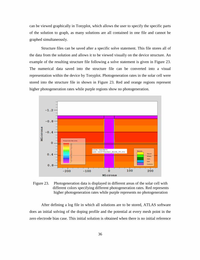
Structure files can be saved after a specific solve statement. This file stores all of
the data from the solution and allows it to be viewed visually on the device structure. An
example of the resulting structure file following a solve statement is given in Figure 23.
The numerical data saved into the structure file can be converted into a visual
representation within the device by Tonyplot. Photogeneration rates in the solar cell were
stored into the structure file in shown in Figure 23. Red and orange regions represent
higher photogeneration rates while purple regions show no photogeneration.
Figure 23. Photogeneration data is displayed in different areas of the solar cell with different colors specifying different photogeneration rates. Red represents higher photogeneration rates while purple represents no photogeneration
After defining a log file in which all solutions are to be stored, ATLAS software
does an initial solving of the doping profile and the potential at every mesh point in the
zero electrode bias case. This initial solution is obtained when there is no initial reference

37
zero bias solution but can be specified by the statement solve init. After this initial solve
statement, the conditions for the specific solve statements can be set. In simulating the
operation of a solar cell, the statement
solve B1=1.0
applies the equivalent of one sun from the earlier defined light source and solves the
pertinent quantities such as photogeneration rates and optical intensities at each mesh
point as well as the electrode currents. After the beam of light has been applied, solutions
at different electrode voltages can be obtained to create the solar cell’s I-V curve. The
statements
solve vanode=0 name=anode vstep=0.1 vfinal=0.7
obtain solutions for the illuminated solar cell at a range of anode voltages. This statement
declares an initial anode voltage of 0 V and obtains solutions in the range of 0 V to 0.7 V
in increments of 0.1 V. By sweeping across anode voltages from 0 V to Voc for the solar
cell, the I-V curve is obtained. An I-V curve obtained by simulating a GaAs solar cell in
ATLAS and sweeping anode voltages is shown in Figure 24. The simulated cell, like real
solar cells, shows a characteristic in which a gradually increasing anode voltage causes
lower net cathode current until the Voc condition.
Figure 24. Anode Voltage is plotted against cathode current for an ATLAS simulated GaAs solar cell

38
C. CHAPTER SUMMARY
How solar cells are simulated in ATLAS software was covered in this chapter.
The cell structure is defined using Deckbuild code, setting the structure mesh, regions,
electrodes, doping levels, and material properties. The conditions for which solutions are
to be obtained can then be set. The ATLAS software then obtains solutions for all solve
statements and saves the results in log files and structure files based on the instructions of
the user.
The method of modeling a CNT layer and including the model in a simulated
solar cell are described in the following chapter.

39
V. MODELLING A HETEROGENEOUS CARBON NANOTUBE LAYER
The method used in modeling a heterogeneous layer of CNTs as a transparent
charge collector in Silvaco ATLAS software is covered in this chapter. Due to the
restrictions associated with modeling materials in ATLAS software, simplifications and
assumptions were made to best simulate a metal-like material with certain conductance
and optical properties. The assumptions made in modeling the CNT layer as well as some
of the experimental data used as the basis for the model are covered in this chapter.
A. BASIS FOR THE CNT MODEL
The model for heterogeneous CNT networks created in this thesis is based on the
experiments of the Institute for Microstructural Science of the National Research Council
of Canada[1]. In these experiments, networks of SWCNTs were deposited onto
polyethylene terephthalate (PET) films by a dip method, and the characteristics of the
CNT networks were measured. This dip method utilized a solution in which a set density
of SWCNTs was present. The PET films were dipped into the solution for ten seconds
and withdrawn at a speed of 0.5 cm/min. The PET film was then baked in a Fisher
isotherm oven at a temperature of 110 Celsius for five minutes. The data of two
heterogeneous networks that were the result of one and two-dip coatings, respectively,
are utilized in this thesis. These CNT networks were tested to obtain their value of sheet
resistance and their level of light transmission. The light transmission of the single and
double-dip coated CNT networks is shown in Figure 25. The single-dip coated CNT
network has a higher value of sheet resistance of 128 ohms per square but higher net light
transmission.

40
Figure 25. The experimental light transmission data of a single-dip coated and double-dip coated CNT network show an inverse relationship between sheet
resistance and light transmission. From [1]
B. MODELING A TRANSPARENT CONDUCTOR IN SILVACO ATLAS
Ideally, a heterogeneous CNT network would be modeled as a metal with the
optical properties and resistivity of the CNT network. However, due to the limitations of
ATLAS software, the CNT network in this thesis is modeled as a low bandgap
semiconductor. The ATLAS software has problems obtaining solutions when a metal
makes contact with an electrode in the specified structure. Since the purpose of this thesis
is to analyze the flow of charge carriers through a semitransparent material, the use of a
semiconductor is optimal because the ATLAS software obtains solutions for all of the
charge carriers moving towards the electrodes in semiconductors.
Though a heterogeneous CNT network does not exhibit semiconductor properties,
the material statements in the ATLAS code can be utilized to create a semiconductor with
metallic properties. In this thesis, 4-H Silicon Carbide (4H-SiC) was chosen as the
semiconductor to alter based on the work of Brunton in the modeling of carbon nanofiber
interconnects in Silvaco Atlas software[12]. To create an accurate model of a CNT

41
network, the material properties of Silicon Carbide were modified to give the material
metallic characteristics while also matching experimental sheet resistance values. Since
altering the optical properties adds unnecessary complications to the material model, the
Silicon Carbide was made to be completely transparent. The input light beam was
modified to instead model the resulting light that would pass through a CNT network
based on experimental light transmission data.
1. Material Properties of the CNT Network Model
The heterogeneous CNT network modeled in this thesis used 4H-SiC as the base
material which has the advantage of being a less commonly used material in ATLAS
software. Because 4H-SiC is less commonly used than other materials in the ATLAS
material library, it has fewer default parameters unimportant to this thesis that could
cause errors in the simulations. The primary parameters which were modified to give the
4H-SiC metallic properties were the band and recombination parameters. The parameters
that were changed in the 4H-SiC are summarized in Table 2.
The band parameters were changed to make the 4H-SiC a material with
essentially no band gap and adjustable hole and electron mobilities to achieve the desired
value of sheet resistance. To give the CNT network material a set value of sheet
resistance, the electron and hole mobilities were modified to change the resistivity of the
material. The resistivity of a semiconductor material is given by
1( )n pq n p
ρµ µ
=+
(6)
where q is the equivalent charge of one electron or hole, µn and µp are the electron and
hole mobilities, respectively, and n and p are the electron and hole concentrations in the
material. The sheet resistance of a material is given by
sRtρ
= (7)
where t is the thickness of the material. The equation for sheet resistance was first used to
solve for the necessary resistivity based upon a thickness of one micron and a sheet
resistance value obtained from experimental data. The electron and hole mobilities were

42
then set equal to each other and solved for in the resistivity equation. Though the electron
and hole mobilities are not equal in a heterogeneous CNT network, the basic creation of a
sheet resistance based upon equal mobilities was adequate for the purposes of this thesis.
The CNT network created in this thesis was an intrinsic, one micron thick layer of 4H-
SiC. To achieve the desired values of sheet resistance, the values of n and p were set at
1017 cm-3, the typical intrinsic carrier concentration of 4H-SiC at room temperature. The
electron and hole mobilities for each value of sheet resistance were calculated to match
the experimental sheet resistances of 75 Ω and 128 Ω and are given in Table 2. In Silvaco
ATLAS, electron and hole mobility are abbreviated as MUN and MUP respectively.
To verify the calculations of sheet resistance, each of the modeled CNT materials
was simulated with 1 V applied across the width of material as shown in Figure 26. The
current was calculated in each case, and the result was used to determine the sheet
resistance of each material. The two values of sheet resistance obtained were 126 Ω and
76 Ω of sheet resistance, which closely match the experimental data which the models are
based on. The final parameters used in the two CNT materials are summarized in Table 2.
Figure 26. The experiment to determine the sheet resistance of the CNT materials is shown

43
Table 2. The material parameters that were changed to give 4H-SiC metallic properties in Silvaco ATLAS are summarized
Parameter Type ATLAS Identifier Value Band Permittivity 5.4
Affinity 5.8
NC300,NV300 3x10¹⁷
NC.F,NV.F 3x10¹⁷ MUN,MUP (126Ω) 8138.02 MUN,MUP (76Ω) 13889
Recombination taun0,taup0 0 nsrhn,nsrhp 0 ksrhcn,ksrhcp 0 ksrhtn,ksrhtp 0 ksrhgn,ksrhgp 0 augn,augp 0 augkn,augkp 0 kaugcn,kaugcp 0 kaugdn,kaugdp 0 Etrap 0 Copt 0
The other material property which significantly affected the functionality of the
CNT network material was the electron affinity. The electron affinity of a material is the
difference between the vacuum energy level and the conduction band energy level of a
material. This property affected the CNT network material by altering the junction with
the neighboring Aluminum Gallium Arsenide (AlGaAs) layer in the solar cell used in this
thesis. Ideally, the CNT network acts as a metal and has a metal-semiconductor junction
characteristic. However, since the CNT network in this thesis was modeled as a
semiconductor, a heterojunction was created between the CNT material and the
neighboring AlGaAs layer. To accurately model a heterogeneous network, the electron
affinity of the material was modified until the functionality of the heterojunction with the
AlGaAs layer most closely resembled the junction of a metal and a semiconductor.
Ideally, this junction would not impede the flow of current, allowing for all generated
charge carriers in a solar cell to reach the top contact. To determine the optimal value of

44
electron affinity, a GaAs solar cell with a top CNT layer was simulated with varying
CNT electron affinity levels. The short circuit currents from these simulations were
compared, and the maximum value was extracted. The electron affinity level of 5.8 eV,
which allowed for the maximum short circuit current, was then set as the electron affinity
level of the CNT material. The top portion of the cell used in the electron affinity
comparison is shown in Figure 27. The cell has a top CNT layer with a neighboring
AlGaAs layer. This same cell was also used in the final experiment of this thesis.
Figure 27. The top portion of the solar cell used in the electron affinity comparison is shown
2. Modeling the Optical Properties
To model the optical properties of a heterogeneous CNT network, the input solar
power in simulations involving a CNT network was altered to model the resultant light
transmitting through the material while leaving the CNT material completely transparent.
To achieve this, the transmission data from the Institute for Microstructural Science of
the National Research Council of Canada was used to apply a series of scale factors to
alter the am0 spectrum at different wavelengths[1]. The am0 spectrum compared with the

45
input spectrums of associated with heterogeneous CNT layers of 76 Ω and 126 Ω of sheet
resistance are shown in Figures 28 and 29. The net drop in input power with the addition
of a CNT layer is shown in Figure 28. The percentage of input power present for a range
of wavelengths in each of the CNT light spectrums relative to am0 is shown in Figure 29.
Figure 28. The am0 spectrum is plotted against the spectrums used in simulation of CNT networks with 126 Ω and 76 Ω of sheet resistance

46
Figure 29. The power level of a range of wavelengths relative to am0 is plotted for the input light of solar cell simulations involving CNT networks of 126 Ω and
76 Ω of sheet resistance
C. EVALUATING THE CNT MODEL IN A SOLAR CELL
In evaluating the CNT model, the most important factors to analyze were the
benefits of having a lower resistance path for charge carriers to travel to the top contact of
a solar cell. Therefore, experiments were set up which compared the performance of a
solar cell with and without a CNT layer while varying certain aspects of the solar cell.
The first experiment compared the current density in different regions of a GaAs solar
cell with and without a CNT layer. This experiment demonstrated that photogenerated
charge carriers were travelling through the CNT layer to the top contact.
To evaluate the performance of a CNT layer in a solar cell, an experiment was set
up so that the solar cell width was varied while keeping the contact width constant in a
GaAs solar cell with and without a CNT layer. The contact width was kept constant at all
solar cell widths to analyze the effects of gradually increasing charge carrier distance to

47
the contact of the solar cell. A visual demonstration of the experiment is given in Figure
30. The width of the cell W was varied while solar cell parameters were obtained for each
width.
Figure 30. A visual demonstration of the experiment used to evaluate the performance of the CNT layer is shown. The cell displayed has a width of 500 microns,
representing one run of the experiment
The pertinent solar cell characteristics gathered in each cell width simulation were
Isc, Voc, Pmax, Vmax, and Imax. These parameters were obtained at each width for a GaAs
solar cell without a CNT layer, the GaAs solar cell with a CNT layer of 126 Ω of sheet
resistance, and the GaAs solar cell with a CNT layer of 76 Ω of sheet resistance. The
parameters were then compared to evaluate the effect of a CNT layer on a GaAs solar
cell.

48
D. CHAPTER SUMMARY
The method of modeling a heterogeneous CNT layer for solar cell applications in
Silvaco ATLAS software was covered in this chapter. The CNT layer was given specific
sheet resistance values by altering the electron and hole mobilities for a constant layer
thickness of one micron. The optical properties of the material were accounted for by
altering the input solar spectrum to the simulated solar cell while keeping the CNT layer
completely transparent. The am0 spectrum was altered so that it matched the resulting
input light power that would transmit through a CNT layer of given sheet resistance
based on experimental spectral data from the Institute for Microstructural Science of the
National Research Council of Canada.
The experiments which were used to evaluate the effects of a CNT layer on the
surface of a solar cell were then described. The current densities of solar cells with and
without top CNT layers were first compared to verify that photogenerated carriers were
travelling to the top contact via the CNT material. A GaAs solar cell with and without a
CNT layer was then simulated with varying solar cell width and a constant contact width.
The pertinent cell parameters were then compared to analyze the effects of a lower
resistance path for charge carriers in the GaAs solar cell. The results of these experiments
are given in the next chapter.

49
VI. RESULTS
The experiments described in the previous chapter were conducted on GaAs solar
cells with and without a top CNT layer. The results were obtained and analyzed to
determine the functionality of the modeled top CNT layer on a solar cell.
A. VERIFICATION OF THE CNT LAYER AS A CHARGE COLLECTOR
A GaAs solar cell was first simulated with and without a CNT layer, and the
current densities in different regions of the cells were analyzed to verify that charge
carriers were travelling in the CNT layer to the top contact. The GaAs solar cell used in
this thesis is based on the work of Crespin[13]. The cells were simulated in the short
circuit condition in which no bias was applied across the electrodes. The gold top contact
was set to be opaque to cause shadowing as in real solar cells. This effect blocks light to a
portion of the cell, preventing photogeneration in the shaded region. The resultant
photogeneration rates for a 500 micron wide GaAs cell with a 50 micron wide gold
contact are shown in Figure 31. The gold contact blocks light to ten percent of the cell,
essentially preventing the generation of charge carriers.
Figure 31. Photogeneration in a GaAs cell with a gold top contact is shown. Red and orange regions have higher photogeneration rates while purple regions
exhibit no photogeneration

50
The total current density in a GaAs solar cell without a CNT Layer is shown in
Figure 32. The current concentrates in the top AlGaAs layer and the GaAs emitter region
when travelling to the top contact. The flow of charge carriers in this region causes a
voltage drop as the charge carriers are affected by the resistance in both of these regions.
Figure 32. Current Density viewed in Tonyplot for a GaAs solar cell is shown
The current density in a GaAs solar cell with a top CNT layer of 126 Ω of sheet
resistance is shown in Figure 33. The current converges in the top CNT layer to travel to
the top contact for charge collection. The charge carriers in this region see less net
resistance in the more highly conducting CNT layer.

51
Figure 33. The current density in a GaAs solar cell with a 126 Ω sheet resistance layer of CNT on the surface is shown
The current density in the GaAs solar cell with a 76 Ω sheet resistance CNT layer
on the surface is shown in Figure 34. Like the 126 Ω CNT layer cell, the current
converges in the top CNT layer as charge carriers travel along the path of least resistance.
Figure 34. The current density in a GaAs solar cell with a 76 Ω sheet resistance layer of CNT on the surface is shown

52
Once the current was shown to travel through the top CNT layer, the I-V
characteristic for the GaAs solar cell was compared with the I-V characteristic of the
GaAs cell including top CNT layers of 126 Ω and 76 Ω of sheet resistance. These solar
cells were all simulated with the inputs outlined in the previous chapter which are based
on the amount of am0 input light present to the solar cell after transmission through a
CNT layer. The cell width was set at 500 microns in these simulations. The ATLAS code
used to simulate the cells is given in the Appendix. The I-V curves for the normal GaAs
solar cell, a cell including a 126 Ω sheet resistance CNT layer and a cell including a 76 Ω
sheet resistance CNT layer are shown in Figure 35. As expected with a smaller cell
width, the cells with the CNT layers have lower current values than the standard GaAs
cell due to the loss of input power caused by the CNT layers. A comparison of solar cell
parameters is given in Table 3.
Figure 35. The I-V curves for the standard GaAs solar cell and GaAs solar cells including top CNT layers of 126 Ω and 76 Ω of sheet resistance are shown

53
Table 3. A summary of the important solar cell parameters is given for the standard 500 micron wide GaAs solar cell and the cell with different CNT layers
Cell Type GaAs 126 Ω CNT 76 Ω CNT Cell Width (μm) 500 500 500
Isc (mA/cm2) 34.691 30.637 26.96 Voc (V) 1.037 1.035 1.031
Pmax (W/cm2) 31.274 27.519 24.163 Vmax (V) 0.94 0.93 0.93
Imax (mA/cm2) 33.272 29.591 25.982
B. VARYING THE CELL WIDTH
The next experiment carried out was outlined in the previous chapter. The GaAs
cell along with the two cells with CNT layers were simulated at varying widths while
gathering the solar cell parameters. The contact width was held at a constant value to
demonstrate the advantages of a lower resistance path for charge carriers at greater cell
widths. In the experiment the cell width was varied from 200 to 4000 microns, and the
contact width was set at 50 microns for all simulations. The full code used in the
simulation is given in the Appendix.
The first cell parameter analyzed for each of the solar cells was the short circuit
current. The short circuit currents for each cell obtained during the simulation are shown
in Figure 36. For each of the cells, the short circuit current gradually increased as the cell
width increased. This result is expected as gradual increases in cell width paired with a
constant contact width result in a gradual decrease in the percentage of the cell being
shaded by the contact. With the minimum simulated cell width of 200 microns, 25
percent of the cell cannot generate charge carriers, while with the maximum cell width of
4000 microns, just over one percent of the cell is shaded.

54
Figure 36. The short circuit current obtained at each cell width simulated is plotted for a GaAs solar cell and cells with 126 Ω and 76 Ω sheet resistance layers
The open circuit voltages of the three solar cells were then analyzed and
compared. The open circuit voltages of the three cells graphed against cell width is
shown in Figure 37. The slight increase in all of the open circuit voltages is caused by the
reduction in shading. As less of the cell is shaded, more charge carriers are generated in
the cell. The open circuit voltage is the voltage caused by the concentration of opposing
charge carriers at the two electrodes of the solar cell. As more charge carriers are
generated, the potential between the two electrodes connected in an open circuit
configuration becomes greater.

55
Figure 37. The open circuit voltage obtained at each cell width simulated is plotted for a GaAs solar cell and cells with 126 Ω and 76 Ω sheet resistance layers
The maximum power values for each solar cell were then obtained and compared
for each cell width and are shown in Figure 28. Each cell reached a maximum Pmax at a
certain width and then showed reductions in Pmax for greater widths. The most
pronounced decline in Pmax for greater cell widths was seen in the GaAs solar cell without
a CNT layer. This sharp decline was due to the voltage losses from resistance in the
AlGaAs and GaAs layers as charge carriers had to travel further to the contact. Since the
CNT layers provided charge carries in the other solar cells with lower resistance paths to
the contact, the reduction in Pmax for greater cell widths was less pronounced.
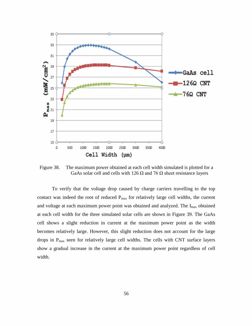
56
Figure 38. The maximum power obtained at each cell width simulated is plotted for a GaAs solar cell and cells with 126 Ω and 76 Ω sheet resistance layers
To verify that the voltage drop caused by charge carriers travelling to the top
contact was indeed the root of reduced Pmax for relatively large cell widths, the current
and voltage at each maximum power point was obtained and analyzed. The Imax obtained
at each cell width for the three simulated solar cells are shown in Figure 39. The GaAs
cell shows a slight reduction in current at the maximum power point as the width
becomes relatively large. However, this slight reduction does not account for the large
drops in Pmax seen for relatively large cell widths. The cells with CNT surface layers
show a gradual increase in the current at the maximum power point regardless of cell
width.

57
Figure 39. The current at the maximum power point obtained at each cell width simulated is plotted for a GaAs solar cell and cells with 126 Ω and 76 Ω
sheet resistance layers
The voltages at the maximum power points were confirmed to be the root of the
reduced Pmax for greater cell widths and were compared to show how cell width created
voltage reduction in the maximum power. The Vmax obtained at each cell width for the
three simulated solar cells are shown in Figure 40. The GaAs solar cell had the greatest
degredation in Vmax with increasing cell width. The lower sheet resistance CNT layer
showed the least amount of Vmax reduction due to the lower voltage losses from charge
carriers travelling to the contact. The two cells with CNT layers on the surface clearly
show an improvement in the maximum power voltage over the GaAs cell.

58
Figure 40. The voltage at the maximum power point obtained at each cell width simulated is plotted for a GaAs solar cell and cells with 126 Ω and 76 Ω
sheet resistance layers
C. CHAPTER SUMMARY
The results of simulations of GaAs cells with CNT layers on the surface of the
cell were presented in this chapter. The results show that the CNT model provides a
lower path of resistance for charge carriers in a solar cell to travel to the top contact. The
lower path of resistance was shown to improve the performance of solar cells with
relatively large widths by reducing the voltage drop caused by charge carriers travelling
to the top contact of a cell.
Though the solar cells with CNT layers did not show a net improvement in
efficiency, the benefits of less voltage loss from charge carriers travelling to the contact
can eventually improve the efficiencies of solar cells as CNT fabrication methods
improve. CNT layers with lower sheet resistance and a higher level of light transmission
can greatly improve the efficiency of solar cells.

59
VII. CONCLUSIONS AND RECOMMENDATIONS
A method of modeling heterogeneous CNT networks in Silvaco ATLAS software
for photovoltaic applications was presented. This model was incorporated into a GaAs
solar cell and was shown to reduce losses from the flow of charge carriers to the top
contact. The unique properties of CNT layers on the surface of solar cells allow for better
charge carrier collection while only losing a portion of light input power based on the
light transmission of the CNT layer.
The experiments in this thesis showed that when a top CNT layer is applied to a
solar cell, current congregates in the top layer and travels to the contact via a lower
resistance path. As the distance charge carriers have to travel to reach the top contact of
solar cell increases, the voltage drop caused by resistance in semiconductor materials was
shown to have a significant effect on the maximum power available from a solar cell. The
addition of a CNT layer was shown to minimize this voltage drop and maintain high
maximum power levels for cells with large distances between contacts. The ability to
have greater separation between top contact grid lines can allow for a reduction of the
shaded area in a solar cell while also maintaining relatively wide metal top contacts in the
contact grid. This is optimal since any other reduction in the shaded area without the
power reductions due to semiconductor resistance in the cell requires thinner metal grid
lines. The flow of current in these grid lines causes losses that increase with a decrease in
grid line thickness. Since a CNT layer allows equivalent or lesser levels of net cell
shading with wider top contacts, grid line losses can be reduced or made constant while
reducing cell shading. This allows for greater overall efficiencies for solar cells.
Solar cells are currently a high priority for the military and the civilian sector as a
viable source of renewable energy and as a power source in remote locations such as
space or isolated regions. Research regarding the improvement in efficiency of solar cells
will continue as nations attempt to generate more renewable energy for domestic use and
new technologies require more power to be available in remote areas.

60
The research in this thesis provides a possible method for increasing the
efficiencies of solar cells. Further research could be conducted either in improving the
CNT model or by optimizing the relationship between transparency and conductivity in
heterogeneous CNT networks to provide the greatest overall efficiency for a solar cell
utilizing a CNT top layer. Improvements in CNT fabrication methods will also improve
the possibilities for optimizing solar cell performance. The model presented in this thesis
is based on specific experimental data from a fabricated CNT network. CNT networks are
gradually improving in terms of transparency and conductivity. These improvements may
allow solar cell efficiencies to be improved.
The model presented in this thesis is based on many simplifications to allow for a
usable model in ATLAS software. Charge carrier mobility was set at a constant
equivalent value for holes and electrons. Heating in the CNT layer was not accounted for
and could affect the conductivity of the layer. Later research could focus on accounting
for all of the physical properties of CNT layers. As more research is conducted on semi-
transparent heterogeneous CNT networks, more data will be available about the physical
properties of the material. These properties could be accounted for in ATLAS software,
which offers a wide variety of physical models for numerous properties.
With the working model for heterogeneous CNT networks presented in this thesis,
supplementary work in the optimization of solar cells is possible. The relationship
between the transparency and conductivity can be used to optimize the efficiency of a
solar cell. By iterating cell simulations of different widths with CNT layers of varying
resistance, a maximum efficiency for different types of solar cells incorporating CNT
layers could be obtained. This work could then be verified by testing on an actual solar
cell to verify the model.
The ability of Silvaco ATLAS software to simulate modeled materials shown in
this and other theses has important implications for the future of solar cell research. New
materials can be modeled and simulated cheaply before large investments are required for
physical tests. Through this modeling and simulation, solar cells can be more cheaply
improved, making them a more viable power source for all applications.

61
APPENDIX
The following Deckbuild code was used to simulate a GaAs solar cell with and
without heterogeneous CNT surface layers. The code uses loop statement to loop through
different cell widths for each type of cell. The results are extracted from each run with
extract statements which import the data to the “results.final” file. This file is
automatically generated by ATLAS. # Adam Garfrerick # Final Experiment evaluating CNT model performance #Definition of constants #Mesh #X-Mesh #Y-Mesh #Regions #Electrodes #Doping #Material Properties #Models #Light Beams #Solving #GaAs solar cell without a CNT Layer #The cell width is initially set at 200 microns. The loop statement is #set to loop the simulation 19 times to extract cell parameters at #varying widths set cellWidth=200 loop steps=19 go atlas #Constants which are used to set the cell parameters are defined set contWidthpercent=10 set divs=10 set emitThick=0.4 set emitDepThick=.04 set baseDepThick=.4 set baseThick=10 set winThick=0.5 set contThick=0.1 set elecThick=0.1 set subThick=10 set emitMax=0 set emitDepMax=$emitMax+$emitDepThick set baseDepMax=$emitDepMax+$baseDepThick set baseMax=$baseDepMax+$baseThick set baseMid=$baseMax-$baseThick/2 set subMax=$baseMax+$subThick set winMax=$emitMax - $emitThick set contMax=$winMax-$winThick

62
set contMin=$contMax-$contThick set elecMin=$contMax-$elecThick set winDop=1e18 set emitDop=1e18 set emitDepDop=1e18 set baseDepDop=1e17 set baseDop=1e17 set subDop=5e17 set cellWidthDiv=$cellWidth/$divs set width3d=100e6/$cellWidth set contWidth=25 set contWidthDiv=$contWidth/($divs) set cellWidthHalf=$cellWidth/2 set contDiv=$contThick/($divs*10) set winDiv=$winThick/$divs set emitDiv=$emitThick/$divs set emitDepDiv=$emitDepThick/$divs set baseDepDiv=$baseDepThick/$divs set baseDiv=$baseThick/$divs set subDiv=$subThick/$divs #Meshing mesh width=$width3d #mesh space.mult=1 #X-mesh: Surface=500 um2 = 1/200000 cm2 x.mesh loc=-$cellWidthHalf spac=$cellWidthDiv x.mesh loc=-$contWidth spac=$contWidthDiv x.mesh loc=$contWidth spac=$contWidthDiv x.mesh loc=$cellWidthHalf spac=$cellWidthDiv #Y-Mesh #Top of Contact y.mesh loc=$contMin spac=$contDiv #Window y.mesh loc=$contMax spac=$contDiv y.mesh loc=$winMax spac=$winDiv # Emitter y.mesh loc=$emitMax spac=$emitDiv # Depletion Region y.mesh loc=$emitDepMax spac=$emitDepDiv y.mesh loc=$baseDepMax spac=$baseDepDiv # Base y.mesh loc=$baseMax spac=$baseDiv # Substrate y.mesh loc=$subMax spac=$subDiv # Regions # Contact #Contact region is initially set as a vacuum region but will be covered #by a gold electrode in the electrode statements

63
region num=1 material=Vacuum x.min=-$contWidth x.max=$contWidth\ y.min=$contMin y.max=$contMax # Empty Space region num=2 material=Vacuum x.min=-$cellWidthHalf x.max=-$contWidth\ y.min=$contMin y.max=$contMax region num=3 material=Vacuum x.min=$contWidth x.max=$cellWidthHalf\ y.min=$contMin y.max=$contMax # Window region num=4 material=AlGaAs x.comp=0.9 x.min=-$cellWidthHalf\ x.max=$cellWidthHalf y.min=$contMax y.max=$winMax # Emitter region num=5 material=GaAs x.min=-$cellWidthHalf x.max=$cellWidthHalf\ y.min=$winMax y.max=$emitMax # Emitter Depletion Region region num=6 material=GaAs x.min=-$cellWidthHalf x.max=$cellWidthHalf\ y.min=$emitMax y.max=$emitDepMax # Base Depletion Region region num=7 material=GaAs x.min=-$cellWidthHalf x.max=$cellWidthHalf\ y.min=$emitDepMax y.max=$baseDepMax # Base region num=8 material=GaAs x.min=-$cellWidthHalf x.max=$cellWidthHalf\ y.min=$baseDepMax y.max=$baseMax # Substrate region num=9 material=GaAs x.min=-$cellWidthHalf x.max=$cellWidthHalf\ y.min=$baseMax y.max=$subMax #Electrodes electrode name=anode material=Gold x.min=-$contWidth x.max=$contWidth\ y.min=$contMin y.max=$contMax electrode name=cathode x.min=-$cellWidthHalf x.max=$cellWidthHalf\ y.min=$subMax y.max=$subMax #Doping # Window doping uniform region=4 p.type conc=$winDop # Emitter doping uniform region=5 p.type conc=$emitDop #Emitter Depletion Region doping uniform region=6 p.type conc=$emitDepDop #BaseDepletion Region doping uniform region=7 n.type conc=$baseDepDop # Base doping uniform region=8 n.type conc=$baseDop # Substrate doping uniform region=9 n.type conc=$subDop #Material Properties material TAUN=1e-7 TAUP=1e-7 COPT=1.5e-10 AUGN=8.3e-32 AUGP=1.8e-31 #Vacuum material material=Vacuum real.index=3.3 imag.index=0 #GaAs

64
material material=GaAs EG300=1.42 PERMITTIVITY=13.1 AFFINITY=4.07 material material=GaAs NC300=4.7e17 NV300=7e18 material material=GaAs sopra=Gaas.nk # AlGaAs material material=AlGaAs EG300=1.5487 PERMITTIVITY=12.616 AFFINITY=3.96 material material=AlGaAs NC300=1.39e18 NV300=9.78e18 COPT=1.8e-10\ TAUN0=4.5e-9 TAUP0=2e-8 material material=AlGaAs sopra=Algaas9.nk # Material Properties #CNT material properties material material=4H-SiC EG300=0.026 PERMITTIVITY=5.4 AFFINITY=5.8 material material=4H-SiC NC300=3e17 NV300=3e17 material material=4H-SiC NC.F=0 NV.F=0 # Recombination Parameters material material=4H-SiC taun=0 taup=0 etrap=0 material material=4H-SiC augn=0 augp=0 material material=4H-SiC augkn=0 augkp=0 material material=4H-SiC kaugcn=0 kaugcp=0 material material=4H-SiC kaugdn=0 kaugdp=0 material material=4H-SiC copt=0 #Optical Parameters material material=4H-SiC real.index=1 imag.index=0 #Gold material material=Gold real.index=1.2 imag.index=1000 #Models models conmob consrh output con.band val.band #Light Beams beam num=1 am0 wavel.start=0.21 wavel.end=4 wavel.num=50 #Output and Display Struct File #Solving log outfile=GaAs_Thermal_cell.log solve init method gummel maxtraps=10 itlimit=25 solve B1=1.0 solve vanode=0 name=anode vstep=0.1 vfinal=0.8 solve vanode=0.8 name=anode vstep=0.01 vfinal=1.05 #Extract the cell characteristics for each cell width #Results will appear in the “results.final” which is the #default file name for extracted values in ATLAS code extract init infile="GaAs_Thermal_cell.log" extract name="opt_int" max(beam."1")

65
extract name="Isc" y.val from curve(V."anode", I."cathode") where\ x.val=0 extract name="Voc" x.val from curve(V."anode", I."cathode") where\ y.val=0 extract name="Pm" max(curve(V."anode",(V."anode"*I."cathode"))) extract name="Vm" x.val from\ curve(V."anode",(V."anode"*I."cathode"))\ where y.val=$"Pm" extract name="Im" $"Pm"/$"Vm" extract name="FF" $"Pm"/($"Isc"*$"Voc") extract name="eff" (abs($"Pm")/$opt_int) #Code will loop again with a wider cell width. Code will loop until set #iterations complete. set cellWidth=$cellWidth + 100 l.end # Begin loop with 126 ohm sheet resistance CNT Layer set cellWidth=200 loop steps=19 go atlas set contWidthpercent=10 set divs=10 set CNTThick=0.1 set emitThick=0.4 set emitDepThick=.04 set baseDepThick=.4 set baseThick=10 set winThick=0.5 set contThick=0.1 set subThick=10 set emitMax=0 set emitDepMax=$emitMax+$emitDepThick set baseDepMax=$emitDepMax+$baseDepThick set baseMax=$baseDepMax+$baseThick set baseMid=$baseMax-$baseThick/2 set subMax=$baseMax+$subThick set winMax=$emitMax - $emitThick set CNTMax=$winMax-$winThick set contMax=$CNTMax-$CNTThick set contMin=$contMax-$contThick set winDop=1e18 set emitDop=1e18 set emitDepDop=1e18 set baseDepDop=1e17 set baseDop=1e17 set subDop=5e17 set cellWidthDiv=$cellWidth/$divs set width3d=100e6/$cellWidth set contWidth=25 set contWidthDiv=$contWidth/($divs)

66
set cellWidthHalf=$cellWidth/2 set contDiv=$contThick/($divs*10) set CNTDiv=$CNTThick/($divs) set winDiv=$winThick/$divs set emitDiv=$emitThick/$divs set emitDepDiv=$emitDepThick/$divs set baseDepDiv=$baseDepThick/$divs set baseDiv=$baseThick/$divs set subDiv=$subThick/$divs #Meshing mesh width=$width3d #mesh space.mult=1 #X-mesh: Surface=500 um2 = 1/200000 cm2 x.mesh loc=-$cellWidthHalf spac=$cellWidthDiv x.mesh loc=-$contWidth spac=$contWidthDiv x.mesh loc=$contWidth spac=$contWidthDiv x.mesh loc=$cellWidthHalf spac=$cellWidthDiv #Y-Mesh #Top of Contact y.mesh loc=$contMin spac=$contDiv #CNT Layer y.mesh loc=$contMax spac=$contDiv #Window y.mesh loc=$CNTMax spac=$CNTDiv y.mesh loc=$winMax spac=$winDiv # Emitter y.mesh loc=$emitMax spac=$emitDiv # Depletion Region y.mesh loc=$emitDepMax spac=$emitDepDiv y.mesh loc=$baseDepMax spac=$baseDepDiv # Base y.mesh loc=$baseMax spac=$baseDiv # Substrate y.mesh loc=$subMax spac=$subDiv # Regions #Contact region num=1 material=Vacuum x.min=-$contWidth x.max=$contWidth\ y.min=$contMin y.max=$contMax # Empty Space region num=2 material=Vacuum x.min=-$cellWidthHalf x.max=-$contWidth\ y.min=$contMin y.max=$contMax region num=3 material=Vacuum x.min=$contWidth x.max=$cellWidthHalf\ y.min=$contMin y.max=$contMax # CNT Layer region num=4 material=4H-Sic x.min=-$cellWidthHalf \ x.max=$cellWidthHalf y.min=$contMax y.max=$CNTMax # Window region num=5 material=AlGaAs x.comp=0.9 x.min=-$cellWidthHalf \ x.max=$cellWidthHalf y.min=$CNTMax y.max=$winMax # Emitter

67
region num=6 material=GaAs x.min=-$cellWidthHalf x.max=$cellWidthHalf\ y.min=$winMax y.max=$emitMax # Emitter Depletion Region region num=7 material=GaAs x.min=-$cellWidthHalf x.max=$cellWidthHalf\ y.min=$emitMax y.max=$emitDepMax # Base Depletion Region region num=8 material=GaAs x.min=-$cellWidthHalf x.max=$cellWidthHalf\ y.min=$emitDepMax y.max=$baseDepMax # Base region num=9 material=GaAs x.min=-$cellWidthHalf x.max=$cellWidthHalf\ y.min=$baseDepMax y.max=$baseMax # Substrate region num=10 material=GaAs x.min=-$cellWidthHalf \ x.max=$cellWidthHalf y.min=$baseMax y.max=$subMax #Electrodes electrode name=anode material=Gold x.min=-$contWidth x.max=$contWidth\ y.min=$contMin y.max=$contMax electrode name=cathode x.min=-$cellWidthHalf x.max=$cellWidthHalf\ y.min=$subMax y.max=$subMax #Doping # Window doping uniform region=5 p.type conc=$winDop # Emitter doping uniform region=6 p.type conc=$emitDop #Emitter Depletion Region doping uniform region=7 p.type conc=$emitDepDop #BaseDepletion Region doping uniform region=8 n.type conc=$baseDepDop # Base doping uniform region=9 n.type conc=$baseDop # Substrate doping uniform region=10 n.type conc=$subDop #Material Properties material TAUN=1e-7 TAUP=1e-7 COPT=1.5e-10 AUGN=8.3e-32 AUGP=1.8e-31 #Vacuum material material=Vacuum real.index=3.3 imag.index=0 AFFINITY=3.96 #GaAs material material=GaAs EG300=1.42 PERMITTIVITY=13.1 AFFINITY=4.07 material material=GaAs NC300=4.7e17 NV300=7e18 material material=GaAs sopra=Gaas.nk # AlGaAs material material=AlGaAs EG300=1.5487 PERMITTIVITY=12.616 AFFINITY=3.96 material material=AlGaAs NC300=1.39e18 NV300=9.78e18 COPT=1.8e-10\ TAUN0=4.5e-9 TAUP0=2e-8 material material=AlGaAs sopra=Algaas9.nk # Material Properties

68
#CNT material properties material material=4H-SiC EG300=0.026 PERMITTIVITY=5.4 AFFINITY=5.8 material material=4H-SiC NC300=3e17 NV300=3e17 material material=4H-SiC NC.F=0 NV.F=0 material material=4H-SiC MUN= 8138.02 MUP=8138.02 # Recombination Parameters material material=4H-SiC taun=0 taup=0 etrap=0 material material=4H-SiC augn=0 augp=0 material material=4H-SiC augkn=0 augkp=0 material material=4H-SiC kaugcn=0 kaugcp=0 material material=4H-SiC kaugdn=0 kaugdp=0 material material=4H-SiC copt=0 #Optical Parameters material material=4H-SiC real.index=3.3 imag.index=0 #Gold material material=Gold real.index=1.2 imag.index=1000 #Models models conmob fldmob models consrh output con.band val.band #Light Beams #Use altered spectrum to account for CNT optical properties beam num=1 power.file=CNT_spectrum.txt wavel.start=0.21 wavel.end=4\ wavel.num=50 #Solving log outfile=CNT_Thermal_cell.log solve init method gummel maxtraps=10 itlimit=25 solve B1=1.0 solve vanode=0 name=anode vstep=0.1 vfinal=0.8 solve vanode=0.8 name=anode vstep=0.01 vfinal=1.05 extract init infile="CNT_Thermal_cell.log" extract name="opt_int" max(beam."1") extract name="Isc" y.val from curve(V."anode", I."cathode") where\ x.val=0 extract name="Voc" x.val from curve(V."anode", I."cathode") where\ y.val=0 extract name="Pm" max(curve(V."anode",(V."anode"*I."cathode"))) extract name="Vm" x.val from curve(V."anode",(V."anode"*I."cathode"))\ where y.val=$"Pm" extract name="Im" $"Pm"/$"Vm" extract name="FF" $"Pm"/($"Isc"*$"Voc") extract name="eff" (abs($"Pm")/$opt_int) set cellWidth=$cellWidth + 100 l.end # Begin loop with 76 ohm sheet resistance CNT Layer set cellWidth=200

69
loop steps=19 go atlas set contWidthpercent=10 set divs=10 set CNTThick=0.1 set emitThick=0.4 set emitDepThick=.04 set baseDepThick=.4 set baseThick=10 set winThick=0.5 set contThick=0.1 set subThick=10 set emitMax=0 set emitDepMax=$emitMax+$emitDepThick set baseDepMax=$emitDepMax+$baseDepThick set baseMax=$baseDepMax+$baseThick set baseMid=$baseMax-$baseThick/2 set subMax=$baseMax+$subThick set winMax=$emitMax - $emitThick set CNTMax=$winMax-$winThick set contMax=$CNTMax-$CNTThick set contMin=$contMax-$contThick set winDop=1e18 set emitDop=1e18 set emitDepDop=1e18 set baseDepDop=1e17 set baseDop=1e17 set subDop=5e17 set cellWidthDiv=$cellWidth/$divs set width3d=100e6/$cellWidth set contWidth=25 set contWidthDiv=$contWidth/($divs) set cellWidthHalf=$cellWidth/2 set contDiv=$contThick/($divs*10) set CNTDiv=$CNTThick/($divs) set winDiv=$winThick/$divs set emitDiv=$emitThick/$divs set emitDepDiv=$emitDepThick/$divs set baseDepDiv=$baseDepThick/$divs set baseDiv=$baseThick/$divs set subDiv=$subThick/$divs #Meshing mesh width=$width3d #mesh space.mult=1 #X-mesh: Surface=500 um2 = 1/200000 cm2 x.mesh loc=-$cellWidthHalf spac=$cellWidthDiv x.mesh loc=-$contWidth spac=$contWidthDiv

70
x.mesh loc=$contWidth spac=$contWidthDiv x.mesh loc=$cellWidthHalf spac=$cellWidthDiv #Y-Mesh #Top of Contact y.mesh loc=$contMin spac=$contDiv #CNT Layer y.mesh loc=$contMax spac=$contDiv #Window y.mesh loc=$CNTMax spac=$CNTDiv y.mesh loc=$winMax spac=$winDiv # Emitter y.mesh loc=$emitMax spac=$emitDiv # Depletion Region y.mesh loc=$emitDepMax spac=$emitDepDiv y.mesh loc=$baseDepMax spac=$baseDepDiv # Base y.mesh loc=$baseMax spac=$baseDiv # Substrate y.mesh loc=$subMax spac=$subDiv # Regions #Contact region num=1 material=Vacuum x.min=-$contWidth x.max=$contWidth\ y.min=$contMin y.max=$contMax # Empty Space region num=2 material=Vacuum x.min=-$cellWidthHalf x.max=-$contWidth\ y.min=$contMin y.max=$contMax region num=3 material=Vacuum x.min=$contWidth x.max=$cellWidthHalf\ y.min=$contMin y.max=$contMax # CNT Layer region num=4 material=4H-Sic x.min=-$cellWidthHalf \ x.max=$cellWidthHalf y.min=$contMax y.max=$CNTMax # Window region num=5 material=AlGaAs x.comp=0.9 x.min=-$cellWidthHalf \ x.max=$cellWidthHalf y.min=$CNTMax y.max=$winMax # Emitter region num=6 material=GaAs x.min=-$cellWidthHalf x.max=$cellWidthHalf\ y.min=$winMax y.max=$emitMax # Emitter Depletion Region region num=7 material=GaAs x.min=-$cellWidthHalf x.max=$cellWidthHalf\ y.min=$emitMax y.max=$emitDepMax # Base Depletion Region region num=8 material=GaAs x.min=-$cellWidthHalf x.max=$cellWidthHalf\ y.min=$emitDepMax y.max=$baseDepMax # Base region num=9 material=GaAs x.min=-$cellWidthHalf x.max=$cellWidthHalf\ y.min=$baseDepMax y.max=$baseMax # Substrate region num=10 material=GaAs x.min=-$cellWidthHalf \ x.max=$cellWidthHalf y.min=$baseMax y.max=$subMax #Electrodes

71
electrode name=anode material=Gold x.min=-$contWidth x.max=$contWidth\ y.min=$contMin y.max=$contMax electrode name=cathode x.min=-$cellWidthHalf x.max=$cellWidthHalf\ y.min=$subMax y.max=$subMax #Doping # Window doping uniform region=5 p.type conc=$winDop # Emitter doping uniform region=6 p.type conc=$emitDop #Emitter Depletion Region doping uniform region=7 p.type conc=$emitDepDop #BaseDepletion Region doping uniform region=8 n.type conc=$baseDepDop # Base doping uniform region=9 n.type conc=$baseDop # Substrate doping uniform region=10 n.type conc=$subDop #Material Properties material TAUN=1e-7 TAUP=1e-7 COPT=1.5e-10 AUGN=8.3e-32 AUGP=1.8e-31 #Vacuum material material=Vacuum real.index=3.3 imag.index=0 AFFINITY=3.96 #GaAs material material=GaAs EG300=1.42 PERMITTIVITY=13.1 AFFINITY=4.07 material material=GaAs NC300=4.7e17 NV300=7e18 material material=GaAs sopra=Gaas.nk # AlGaAs material material=AlGaAs EG300=1.5487 PERMITTIVITY=12.616 AFFINITY=3.96 material material=AlGaAs NC300=1.39e18 NV300=9.78e18 COPT=1.8e-10\ TAUN0=4.5e-9 TAUP0=2e-8 material material=AlGaAs sopra=Algaas9.nk #CNT material properties material material=4H-SiC EG300=0.026 PERMITTIVITY=5.4 AFFINITY=5.8 material material=4H-SiC NC300=3e17 NV300=3e17 material material=4H-SiC NC.F=0 NV.F=0 material material=4H-SiC MUN=13889 MUP=13889 # Recombination Parameters material material=4H-SiC taun=0 taup=0 etrap=0 material material=4H-SiC augn=0 augp=0 material material=4H-SiC augkn=0 augkp=0 material material=4H-SiC kaugcn=0 kaugcp=0 material material=4H-SiC kaugdn=0 kaugdp=0 material material=4H-SiC copt=0 #Optical Parameters material material=4H-SiC real.index=3.3 imag.index=0 #Gold

72
material material=Gold real.index=1.2 imag.index=1000 #Models models conmob fldmob models consrh output con.band val.band #Light Beams #Use altered light beam to account for CNT optical properties beam num=1 power.file=CNT_spectrum2.txt wavel.start=0.21 wavel.end=4\ wavel.num=50 #Solving log outfile=CNT_Thermal_cell.log solve init method gummel maxtraps=10 itlimit=25 solve B1=1.0 solve vanode=0 name=anode vstep=0.1 vfinal=0.8 solve vanode=0.8 name=anode vstep=0.01 vfinal=1.05 extract init infile="CNT_Thermal_cell.log" extract name="opt_int" max(beam."1") extract name="Isc" y.val from curve(V."anode", I."cathode") where\ x.val=0 extract name="Voc" x.val from curve(V."anode", I."cathode") where\ y.val=0 extract name="Pm" max(curve(V."anode",(V."anode"*I."cathode"))) extract name="Vm" x.val from curve(V."anode",(V."anode"*I."cathode"))\ where y.val=$"Pm" extract name="Im" $"Pm"/$"Vm" extract name="FF" $"Pm"/($"Isc"*$"Voc") extract name="eff" (abs($"Pm")/$opt_int) set cellWidth=$cellWidth + 100 l.end

73
LIST OF REFERENCES
[1] G. Xiao, Y. Tao; J. Lu; Z. Zhang, "Highly transparent and conductive carbon nanotube coatings deposited on flexible polymer substrate by solution method," Proc. 3rd International Nanoelectronics Conference (INEC), pp.208–209, 3–8 Jan. 2010.
[2] J. Guo, “Carbon Nanotube Electronics, Modeling, Physics, and Applications,” Doctoral Dissertation, Purdue University, 2004.
[3] B. Zeghbroeck, Principles of Electronic Devices, http://ecee.colorado.edu (accessed March 4, 2012).
[4] A. Bates, “Novel Optimization Techniques for Multijunction Solar Cell Design USING SILVACO ATLAS,” Master’s Thesis, Naval Postgraduate School, 2004.
[5] S. Michael, EC3230 Lecture Notes, Naval Postgraduate School, Winter 2004 (unpublished).
[6] S. Michael, “The Design and Optimization of Advanced Multijunction Solar Cells,” Presented at the 35th IEEE PV Specialists Conference, Vancouver, Canada, 2004.
[7] S. Iijima, “Helical Microtubules of Graphitic Carbon,” Nature, vol. 354, pp. 56−58, 1991.
[8] N. Srivastava, R. V. Joshi, and K. Banerjee, “Carbon Nanotube Interconnects: Implications for Performance, Power Dissipation and Thermal Management,” Electron Devices Meeting. IEDM Technical Digest, pp. 249−252, 2005.
[9] M. S. Dresselhaus, G. Dresselhaus, and R. Saito, “Physics of Carbon Nanotubes,” Carbon, vol. 33, no. 7, pp. 883−891, 1995.
[10] A. Alam, M. Chowalla, N. Pimparkar, “Device Optimization for Organic Photovoltaics with CNT Networks as Transparent Electode,” Proc. 33rd IEEE, Photovoltaic Specialists Conference, pp.1–4, 11–16 May 2008.
[11] Renewable Resource Data Center (RReDC). “Solar Spectra: Air Mass Zero,” http://rredc.nrel.gov/solar/spectra/am0/ (accessed April 17, 2012).
[12] J. Brunton, “TCAD Analysis of Heating and Maximum Current Density in Carbon Nanofiber Interconnects,” Master’s Thesis, Naval Postgraduate School, 2011.

74
[13] A. Crespin, “A Novel Approach to Modeling the Effects of Radiation in Gallium-Arsenide Solar Cells Using Silvaco's Atlas Software,” Master’s Thesis, Naval Postgraduate School, 2004.

75
INITIAL DISTRIBUTION LIST
1. Defense Technical Information Center Ft. Belvoir, Virginia 2. Dudley Knox Library Naval Postgraduate School Monterey, California 3. Dr. Clark Robertson, Chairman Department of Electrical and Computer Engineering Naval Postgraduate School Monterey, California 4. Dr. Sherif Michael, Professor Department of Electrical and Computer Engineering Naval Postgraduate School Monterey, California 5. Dr. Sebastian Osswald, Professor Department of Physics Naval Postgraduate School Monterey, California 6. ENS Adam Garfrerick Florence, Alabama