THÈSE DE DOCTORAT DE
183
T HÈSE DE DOCTORAT DE LE MANS UNIVERSITÉ ÉCOLE DOCTORALE N O 596 Matière, Molécules, Matériaux Spécialité : Physique, Ondes et Matériaux Par Artem LEVCHUK "Probing and controlling coherent-phonon and spin-charge conversion in nanostructures with ultrafast visible and THz light pulses" Thèse présentée et soutenue à Le Mans, le 10 mars 2022 Unité de recherche : Institut des Molécules et Matériaux du Mans, UMR CNRS 6283 Thèse N o : 2022LEMA1002 Rapporteurs avant soutenance : Steven JOHNSON Professeur, ETH Zurich Luca PERFETTI Professeur, Laboratoire des Solides Irradiés École polytechnique Composition du Jury : Président : Arnaud ARBOUET Directeur de Recherche CNRS, CEMES-Toulouse Examinateur : Christine BOEGLIN Directrice de Recherche CNRS, IPCMS-Univ Strasbourg Dir. de thèse : Pascal RUELLO Professeur, IMMM-Le Mans Université Co-dir. de thèse : Vincent JUVÉ Chargé de Recherche CNRS, IMMM-Le Mans Université
-
Upload
khangminh22 -
Category
Documents
-
view
0 -
download
0
Transcript of THÈSE DE DOCTORAT DE

THÈSE DE DOCTORAT DE
LE MANS UNIVERSITÉ
ÉCOLE DOCTORALE NO 596Matière, Molécules, MatériauxSpécialité : Physique, Ondes et Matériaux
Par
Artem LEVCHUK
"Probing and controlling coherent-phonon and spin-chargeconversion in nanostructures with ultrafast visible and THz lightpulses"
Thèse présentée et soutenue à Le Mans, le 10 mars 2022Unité de recherche : Institut des Molécules et Matériaux du Mans, UMR CNRS 6283Thèse No : 2022LEMA1002
Rapporteurs avant soutenance :
Steven JOHNSON Professeur, ETH ZurichLuca PERFETTI Professeur, Laboratoire des Solides Irradiés École polytechnique
Composition du Jury :Président : Arnaud ARBOUET Directeur de Recherche CNRS, CEMES-ToulouseExaminateur : Christine BOEGLIN Directrice de Recherche CNRS, IPCMS-Univ StrasbourgDir. de thèse : Pascal RUELLO Professeur, IMMM-Le Mans UniversitéCo-dir. de thèse : Vincent JUVÉ Chargé de Recherche CNRS, IMMM-Le Mans Université

Acknowledgments
This long-short four-year journey was not possible without the help of manypeople. This brief letter is to express my most profound gratitude for their contri-butions to this work.
First and foremost, I sincerely thank my supervisors, Dr. Vincent Juvé andProf. Dr. Pascal Ruello, for giving me the possibility to carry out this work. Fur-thermore, I sincerely appreciate their constant scientific, experimental, and personalguidance, which made the completion of this Ph.D. project possible. Moreover, Iam immensely thankful for their availability, patience and encouragement, especiallyduring the final steps of the manuscript and defense preparation. I could not havehoped for better supervisors and mentors.
I sincerely thank Prof. Dr. Steven Johnson, Prof. Dr. Luca Perfetti, Dr.Arnaud Arbouet, and Dr. Christine Boeglin for being the jury members. I highlyappreciate their effort to come to Le Mans, time spent reading the manuscript, pro-found questions, and valuable suggestions about the work.
In addition, I want to acknowledge the enormous technical help and supportprovided by Dr. Gwenaëlle Vaudel. She was the one who has kept the main lasersystem running in a stable condition, allowing me to carry out the experiments ona daily basis. In addition, her reactivity and responsivity have simplified and accel-erated the resolution of numerous problems.
Essentially, the experimental work carried out in the past four years was im-possible without the high-quality samples. I thank Dr. Mathieu Edely for the in-labgrowth of the thin metallic films of Aluminum and Chromium. In addition, I want toacknowledge our colleagues from the University of Silesia in Katowice for supplyingus with beautiful nanofilms of Bismuth Telluride: Dr. Bartosz Wilk, Dr. MateuszWeis, Dr. Katarzyna Balin, and Pof. Dr. Jacek Szade.
Ultimately, our fruitful collaboration with CEA SPEC in the frame of theANR SANTA project has allowed us to investigate and understand the complexphysics in a multitude of thin magnetic heterostructures. Given this opportunity,I want to acknowledge Dr. Michel Viret, Dr. Jean-Yves Chauleau, Dr. Aurélie
i
ii
Solignac, and Dr. Jean-Baptiste Moussy.
Furthermore, I would like to thank all members of the Institut des Moléculeset Matériaux du Mans, and especially the past and present NoVA team researchers,for their help and assistance. I can not factor out the vital theoretical contributionof Prof. Dr. Brice Arnaud and Dr. Rémi Busselez. Their valuable academic inputsand suggestions have stimulated some experiments and setup developments. A spe-cial thank goes to the Dr. Mads Weber for his constant encouragement and selflesshelp. Besides, I am thankful to Christiane Berne, Maxime Geoffroy, and DanielleChoplin for their assistance in the administrative part of this work.
My deep gratitude goes to my fellow labmates Yevheniia Chernukha, ThomasPerrault, Alexandr Alekhin, and Tadele Otomalo for the long, fruitful discussions,sometimes a necessary distraction from work, and invaluable help. Additionally,I appreciate the endless support of my friends Danylo Babich, Rostyslav Danylo,Pavel Leshuk, Anton Pylypenko, Artem Husiev, and Vadym Voytsekhovsky.
Last but not least, all of this would not have been possible without the constantencouragement and moral support of my beloved family: Irina, Andriy, Anton, Irina,Alexandr, Anatoliy, and Ludmila. In addition, I express my gratitude to Noémie,Sylvain, Marie, and Emilen, that have been by my side all along this journey.
I am grateful for the financial support of the French Ministry of Higher Edu-cation, Research and Innovation.
Contents
Acknowledgments i
List of Figures v
Introduction 1
1 Theoretical background 31.1 Introduction . . . . . . . . . . . . . . . . . . . . . . . . . . . . . . . . . . . . . . . . 31.2 Atoms, electrons, and spins in condensed matter . . . . . . . . . . . . . . . . . . . 4
1.2.1 Ionic subsystem . . . . . . . . . . . . . . . . . . . . . . . . . . . . . . . . . . 51.2.2 Electronic subsystem . . . . . . . . . . . . . . . . . . . . . . . . . . . . . . . 81.2.3 Spin subsystem . . . . . . . . . . . . . . . . . . . . . . . . . . . . . . . . . . 13
1.3 Light-matter interaction . . . . . . . . . . . . . . . . . . . . . . . . . . . . . . . . . 201.3.1 Optical properties and dielectric function . . . . . . . . . . . . . . . . . . . 201.3.2 Polarization, reflection, and transmission of an electromagnetic wave . . . . 321.3.3 Temporal evolution of optical properties . . . . . . . . . . . . . . . . . . . . 35
2 Experimental Methods 392.1 Introduction . . . . . . . . . . . . . . . . . . . . . . . . . . . . . . . . . . . . . . . . 392.2 Pump-probe spectroscopy . . . . . . . . . . . . . . . . . . . . . . . . . . . . . . . . 392.3 Terahertz generation and detection . . . . . . . . . . . . . . . . . . . . . . . . . . . 42
2.3.1 Terahertz generation: optical rectification . . . . . . . . . . . . . . . . . . . 432.3.2 Electrooptic terahertz detection . . . . . . . . . . . . . . . . . . . . . . . . . 45
2.4 THz time-domain spectroscopy . . . . . . . . . . . . . . . . . . . . . . . . . . . . . 532.5 THz pulse shaping . . . . . . . . . . . . . . . . . . . . . . . . . . . . . . . . . . . . 56
3 Ultrafast generation of acoustic and optical phonons with THz 613.1 Introduction . . . . . . . . . . . . . . . . . . . . . . . . . . . . . . . . . . . . . . . . 613.2 Acoustic phonons generation by pulsed THz radiation . . . . . . . . . . . . . . . . 63
3.2.1 Theoretical Background . . . . . . . . . . . . . . . . . . . . . . . . . . . . . 633.2.2 Results and discussion . . . . . . . . . . . . . . . . . . . . . . . . . . . . . . 673.2.3 Conclusions . . . . . . . . . . . . . . . . . . . . . . . . . . . . . . . . . . . . 76
3.3 Coherent optical phonon generation in Bi2Te3 with pulsed THz radiation . . . . . 773.3.1 Theoretical background . . . . . . . . . . . . . . . . . . . . . . . . . . . . . 773.3.2 Results and discussion . . . . . . . . . . . . . . . . . . . . . . . . . . . . . . 823.3.3 Conclusion . . . . . . . . . . . . . . . . . . . . . . . . . . . . . . . . . . . . 91
iii
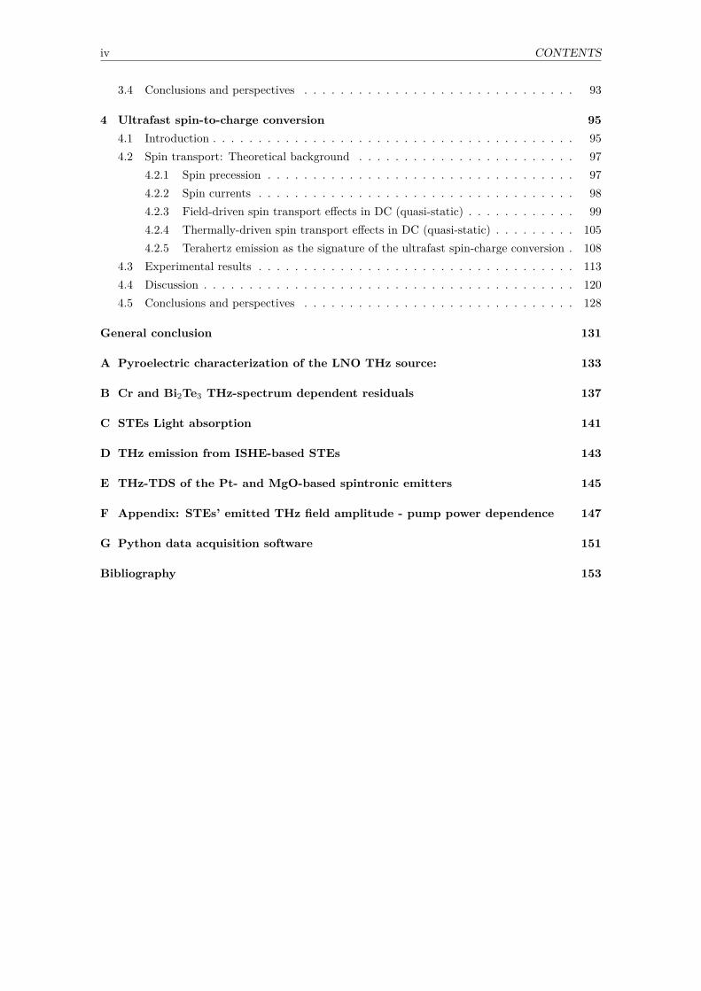
iv CONTENTS
3.4 Conclusions and perspectives . . . . . . . . . . . . . . . . . . . . . . . . . . . . . . 93
4 Ultrafast spin-to-charge conversion 954.1 Introduction . . . . . . . . . . . . . . . . . . . . . . . . . . . . . . . . . . . . . . . . 954.2 Spin transport: Theoretical background . . . . . . . . . . . . . . . . . . . . . . . . 97
4.2.1 Spin precession . . . . . . . . . . . . . . . . . . . . . . . . . . . . . . . . . . 974.2.2 Spin currents . . . . . . . . . . . . . . . . . . . . . . . . . . . . . . . . . . . 984.2.3 Field-driven spin transport effects in DC (quasi-static) . . . . . . . . . . . . 994.2.4 Thermally-driven spin transport effects in DC (quasi-static) . . . . . . . . . 1054.2.5 Terahertz emission as the signature of the ultrafast spin-charge conversion . 108
4.3 Experimental results . . . . . . . . . . . . . . . . . . . . . . . . . . . . . . . . . . . 1134.4 Discussion . . . . . . . . . . . . . . . . . . . . . . . . . . . . . . . . . . . . . . . . . 1204.5 Conclusions and perspectives . . . . . . . . . . . . . . . . . . . . . . . . . . . . . . 128
General conclusion 131
A Pyroelectric characterization of the LNO THz source: 133
B Cr and Bi2Te3 THz-spectrum dependent residuals 137
C STEs Light absorption 141
D THz emission from ISHE-based STEs 143
E THz-TDS of the Pt- and MgO-based spintronic emitters 145
F Appendix: STEs’ emitted THz field amplitude - pump power dependence 147
G Python data acquisition software 151
Bibliography 153
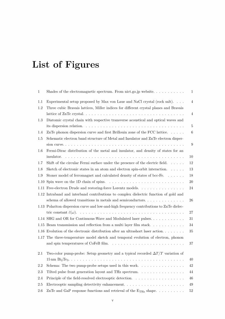
List of Figures
1 Shades of the electromagnetic spectrum. From nict.go.jp website. . . . . . . . . . . 1
1.1 Experimental setup proposed by Max von Laue and NaCl crystal (rock salt). . . . 41.2 Three cubic Bravais lattices, Miller indices for different crystal planes and Bravais
lattice of ZnTe crystal. . . . . . . . . . . . . . . . . . . . . . . . . . . . . . . . . . . 41.3 Diatomic crystal chain with respective transverse acoustical and optical waves and
its dispersion relation. . . . . . . . . . . . . . . . . . . . . . . . . . . . . . . . . . . 51.4 ZnTe phonon dispersion curve and first Brillouin zone of the FCC lattice. . . . . . 61.5 Schematic electron band structure of Metal and Insulator and ZnTe electron disper-
sion curve. . . . . . . . . . . . . . . . . . . . . . . . . . . . . . . . . . . . . . . . . . 91.6 Fermi-Dirac distribution of the metal and insulator, and density of states for an
insulator. . . . . . . . . . . . . . . . . . . . . . . . . . . . . . . . . . . . . . . . . . 101.7 Shift of the circular Fermi surface under the presence of the electric field. . . . . . 121.8 Sketch of electronic states in an atom and electron spin-orbit interaction. . . . . . 131.9 Stoner model of ferromagnet and calculated density of states of bcc-Fe. . . . . . . 181.10 Spin wave on the 1D chain of spins. . . . . . . . . . . . . . . . . . . . . . . . . . . 201.11 Free-electron Drude and restoring-force Lorentz models. . . . . . . . . . . . . . . . 241.12 Intraband and interband contributions to complex dielectric function of gold and
schema of allowed transitions in metals and semiconductors. . . . . . . . . . . . . . 261.13 Polariton dispersion curve and low-and-high frequency contributions to ZnTe dielec-
tric constant ε(ω). . . . . . . . . . . . . . . . . . . . . . . . . . . . . . . . . . . . . 271.14 SHG and OR for Continuous-Wave and Modulated laser pulses. . . . . . . . . . . . 311.15 Beam transmission and reflection from a multi layer film stack. . . . . . . . . . . . 341.16 Evolution of the electronic distribution after an ultrashort laser action. . . . . . . . 351.17 The three-temperature model sketch and temporal evolution of electron, phonon
and spin temperatures of CoFeB film. . . . . . . . . . . . . . . . . . . . . . . . . . 37
2.1 Two-color pump-probe: Setup geometry and a typical recorded ∆T/T variation of15 nm Bi2Te3. . . . . . . . . . . . . . . . . . . . . . . . . . . . . . . . . . . . . . . . 40
2.2 Schema: The two pump-probe setups used in this work. . . . . . . . . . . . . . . . 422.3 Tilted pulse front generation layout and THz spectrum. . . . . . . . . . . . . . . . 442.4 Principle of the field-resolved electrooptic detection. . . . . . . . . . . . . . . . . . 462.5 Electrooptic sampling detectivity enhancement. . . . . . . . . . . . . . . . . . . . . 492.6 ZnTe and GaP response functions and retrieval of the ETHz shape. . . . . . . . . . 52
v
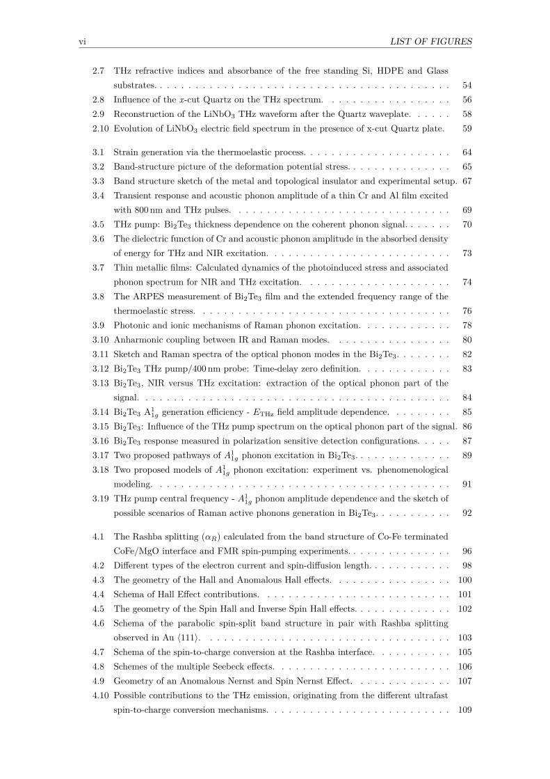
vi LIST OF FIGURES
2.7 THz refractive indices and absorbance of the free standing Si, HDPE and Glasssubstrates. . . . . . . . . . . . . . . . . . . . . . . . . . . . . . . . . . . . . . . . . . 54
2.8 Influence of the x-cut Quartz on the THz spectrum. . . . . . . . . . . . . . . . . . 562.9 Reconstruction of the LiNbO3 THz waveform after the Quartz waveplate. . . . . . 582.10 Evolution of LiNbO3 electric field spectrum in the presence of x-cut Quartz plate. 59
3.1 Strain generation via the thermoelastic process. . . . . . . . . . . . . . . . . . . . . 643.2 Band-structure picture of the deformation potential stress. . . . . . . . . . . . . . . 653.3 Band structure sketch of the metal and topological insulator and experimental setup. 673.4 Transient response and acoustic phonon amplitude of a thin Cr and Al film excited
with 800 nm and THz pulses. . . . . . . . . . . . . . . . . . . . . . . . . . . . . . . 693.5 THz pump: Bi2Te3 thickness dependence on the coherent phonon signal. . . . . . . 703.6 The dielectric function of Cr and acoustic phonon amplitude in the absorbed density
of energy for THz and NIR excitation. . . . . . . . . . . . . . . . . . . . . . . . . . 733.7 Thin metallic films: Calculated dynamics of the photoinduced stress and associated
phonon spectrum for NIR and THz excitation. . . . . . . . . . . . . . . . . . . . . 743.8 The ARPES measurement of Bi2Te3 film and the extended frequency range of the
thermoelastic stress. . . . . . . . . . . . . . . . . . . . . . . . . . . . . . . . . . . . 763.9 Photonic and ionic mechanisms of Raman phonon excitation. . . . . . . . . . . . . 783.10 Anharmonic coupling between IR and Raman modes. . . . . . . . . . . . . . . . . 803.11 Sketch and Raman spectra of the optical phonon modes in the Bi2Te3. . . . . . . . 823.12 Bi2Te3 THz pump/400 nm probe: Time-delay zero definition. . . . . . . . . . . . . 833.13 Bi2Te3, NIR versus THz excitation: extraction of the optical phonon part of the
signal. . . . . . . . . . . . . . . . . . . . . . . . . . . . . . . . . . . . . . . . . . . . 843.14 Bi2Te3 A1
1g generation efficiency - ETHz field amplitude dependence. . . . . . . . . 853.15 Bi2Te3: Influence of the THz pump spectrum on the optical phonon part of the signal. 863.16 Bi2Te3 response measured in polarization sensitive detection configurations. . . . . 873.17 Two proposed pathways of A1
1g phonon excitation in Bi2Te3. . . . . . . . . . . . . . 893.18 Two proposed models of A1
1g phonon excitation: experiment vs. phenomenologicalmodeling. . . . . . . . . . . . . . . . . . . . . . . . . . . . . . . . . . . . . . . . . . 91
3.19 THz pump central frequency - A11g phonon amplitude dependence and the sketch of
possible scenarios of Raman active phonons generation in Bi2Te3. . . . . . . . . . . 92
4.1 The Rashba splitting (αR) calculated from the band structure of Co-Fe terminatedCoFe/MgO interface and FMR spin-pumping experiments. . . . . . . . . . . . . . . 96
4.2 Different types of the electron current and spin-diffusion length. . . . . . . . . . . . 984.3 The geometry of the Hall and Anomalous Hall effects. . . . . . . . . . . . . . . . . 1004.4 Schema of Hall Effect contributions. . . . . . . . . . . . . . . . . . . . . . . . . . . 1014.5 The geometry of the Spin Hall and Inverse Spin Hall effects. . . . . . . . . . . . . . 1024.6 Schema of the parabolic spin-split band structure in pair with Rashba splitting
observed in Au ⟨111⟩. . . . . . . . . . . . . . . . . . . . . . . . . . . . . . . . . . . 1034.7 Schema of the spin-to-charge conversion at the Rashba interface. . . . . . . . . . . 1054.8 Schemes of the multiple Seebeck effects. . . . . . . . . . . . . . . . . . . . . . . . . 1064.9 Geometry of an Anomalous Nernst and Spin Nernst Effect. . . . . . . . . . . . . . 1074.10 Possible contributions to the THz emission, originating from the different ultrafast
spin-to-charge conversion mechanisms. . . . . . . . . . . . . . . . . . . . . . . . . . 109
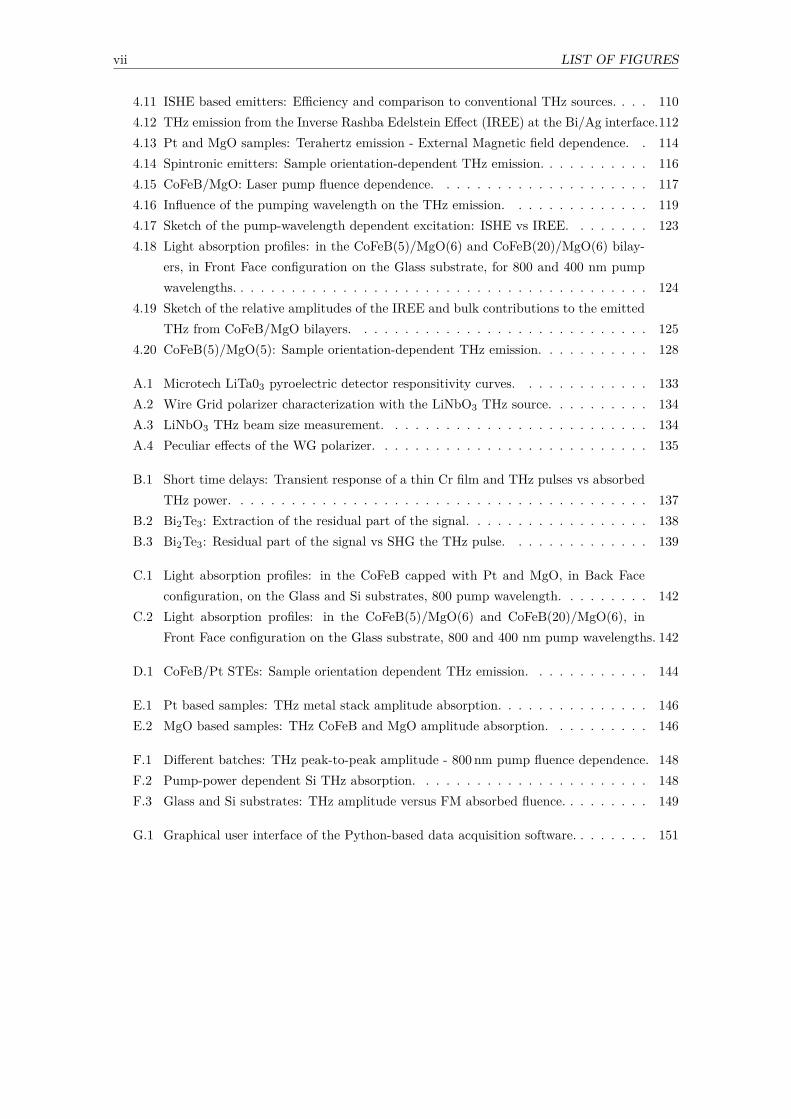
vii LIST OF FIGURES
4.11 ISHE based emitters: Efficiency and comparison to conventional THz sources. . . . 1104.12 THz emission from the Inverse Rashba Edelstein Effect (IREE) at the Bi/Ag interface.1124.13 Pt and MgO samples: Terahertz emission - External Magnetic field dependence. . 1144.14 Spintronic emitters: Sample orientation-dependent THz emission. . . . . . . . . . . 1164.15 CoFeB/MgO: Laser pump fluence dependence. . . . . . . . . . . . . . . . . . . . . 1174.16 Influence of the pumping wavelength on the THz emission. . . . . . . . . . . . . . 1194.17 Sketch of the pump-wavelength dependent excitation: ISHE vs IREE. . . . . . . . 1234.18 Light absorption profiles: in the CoFeB(5)/MgO(6) and CoFeB(20)/MgO(6) bilay-
ers, in Front Face configuration on the Glass substrate, for 800 and 400 nm pumpwavelengths. . . . . . . . . . . . . . . . . . . . . . . . . . . . . . . . . . . . . . . . . 124
4.19 Sketch of the relative amplitudes of the IREE and bulk contributions to the emittedTHz from CoFeB/MgO bilayers. . . . . . . . . . . . . . . . . . . . . . . . . . . . . 125
4.20 CoFeB(5)/MgO(5): Sample orientation-dependent THz emission. . . . . . . . . . . 128
A.1 Microtech LiTa03 pyroelectric detector responsitivity curves. . . . . . . . . . . . . 133A.2 Wire Grid polarizer characterization with the LiNbO3 THz source. . . . . . . . . . 134A.3 LiNbO3 THz beam size measurement. . . . . . . . . . . . . . . . . . . . . . . . . . 134A.4 Peculiar effects of the WG polarizer. . . . . . . . . . . . . . . . . . . . . . . . . . . 135
B.1 Short time delays: Transient response of a thin Cr film and THz pulses vs absorbedTHz power. . . . . . . . . . . . . . . . . . . . . . . . . . . . . . . . . . . . . . . . . 137
B.2 Bi2Te3: Extraction of the residual part of the signal. . . . . . . . . . . . . . . . . . 138B.3 Bi2Te3: Residual part of the signal vs SHG the THz pulse. . . . . . . . . . . . . . 139
C.1 Light absorption profiles: in the CoFeB capped with Pt and MgO, in Back Faceconfiguration, on the Glass and Si substrates, 800 pump wavelength. . . . . . . . . 142
C.2 Light absorption profiles: in the CoFeB(5)/MgO(6) and CoFeB(20)/MgO(6), inFront Face configuration on the Glass substrate, 800 and 400 nm pump wavelengths. 142
D.1 CoFeB/Pt STEs: Sample orientation dependent THz emission. . . . . . . . . . . . 144
E.1 Pt based samples: THz metal stack amplitude absorption. . . . . . . . . . . . . . . 146E.2 MgO based samples: THz CoFeB and MgO amplitude absorption. . . . . . . . . . 146
F.1 Different batches: THz peak-to-peak amplitude - 800 nm pump fluence dependence. 148F.2 Pump-power dependent Si THz absorption. . . . . . . . . . . . . . . . . . . . . . . 148F.3 Glass and Si substrates: THz amplitude versus FM absorbed fluence. . . . . . . . . 149
G.1 Graphical user interface of the Python-based data acquisition software. . . . . . . . 151

Introduction
Solid-state physics at the nanoscale has attracted considerable scientific and industrial interestover the past century. Today, we see an exponential increase in the amount of data generated,stored, and transmitted both locally and all around the web. However, in addition to the ever-increasing computational complexity, the question of the most powerful, robust, and energy-efficientcore for future electronics remains unanswered. As chipmakers relentlessly pursue Moore’s Law,advances in pulsed femtosecond lasers have allowed scientists to study physical processes six timesfaster than the clock speed of the best processors on the market. Ultimately, the rapid developmentin ultrashort lasers has defined new research directions in nanophotonics, solid-state physics, andspintronics. Therefore, understanding the ultrafast coupling between electrons, phonons, and spinsin nanostructures is vital for new promising solutions to the numerous technological challenges.
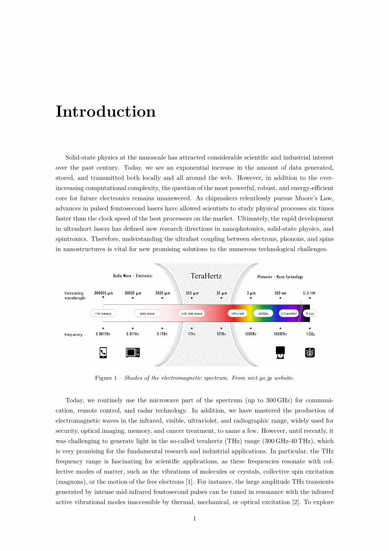
Figure 1 – Shades of the electromagnetic spectrum. From nict.go.jp website.
Today, we routinely use the microwave part of the spectrum (up to 300 GHz) for communi-cation, remote control, and radar technology. In addition, we have mastered the production ofelectromagnetic waves in the infrared, visible, ultraviolet, and radiographic range, widely used forsecurity, optical imaging, memory, and cancer treatment, to name a few. However, until recently, itwas challenging to generate light in the so-called terahertz (THz) range (300 GHz-40 THz), whichis very promising for the fundamental research and industrial applications. In particular, the THzfrequency range is fascinating for scientific applications, as these frequencies resonate with col-lective modes of matter, such as the vibrations of molecules or crystals, collective spin excitation(magnons), or the motion of the free electrons [1]. For instance, the large amplitude THz transientsgenerated by intense mid-infrared femtosecond pulses can be tuned in resonance with the infraredactive vibrational modes inaccessible by thermal, mechanical, or optical excitation [2]. To explore
1
2 INTRODUCTION
such intricate THz-matter interaction, developing the efficient, broadband, and tunable source ofthe pulsed THz radiation is a priority task. For example, it has been shown that femtosecond laserillumination of nm-thick magnetic heterostructures with strong spin-orbit interaction can lead tobroadband THz emission with a tunable polarization state [3]. Furthermore, the selective controlover subtle modulations of the matter’s vibrational, electric, and magnetic properties, possiblyachievable with the THz, is of particular interest for high-performance and low-power electronics.This thesis will contribute to both aspects of THz physics: the excitation of vibrational modes ofa solid with THz pulses and the characterization of the promising spintronic THz emitters.
The first part of this thesis will be devoted to the experimental study of the coherent generationof acoustic phonons with picosecond pulsed THz radiation. Using ultrafast nonlinear spectroscopyin a pump-probe geometry, we will study the transient response of metal films (Cr, Al) and anarrow bandgap, n-doped topological insulator (Bi2Te3) at the picosecond time scale. Through aquantitative comparison between terahertz (4 meV) and near-infrared (1.5 eV) excitation, we willshow that the acoustic phonon generation process in thin metal films with THz is mainly drivenby thermoelastic stress caused by the ultrafast Joule heating of the lattice. To the best of ourknowledge, it is the first demonstration of the THz-driven coherent acoustic phonons in metalsand narrow-band semiconductors.
The following discussion will focus on the rich lattice dynamics when the terahertz pulse excitesthe Bi2Te3 nanofilm. We will demonstrate the non-resonant generation of coherent Raman activephonons, with frequencies up to five times higher than the center frequency of the driving THzpulse. Thus, this work contributes to the description of emerging nonlinear solid-state phononicsand discusses different physical mechanisms of the selective control of the lattice vibrations withTHz light.
The third cornerstone of this thesis aims to detect the ultrafast signature of the spin-chargeinterconversion due to the spin transport in the bulk of CoFeB combined with the injection-based spin-to-charge conversion mechanisms. In particular, the study will be focused on the sub-picosecond dynamics of the recently discovered Rashba-split band structure at the CoFeB/MgOinterface [4]. Therefore, this thesis will try to probe the THz emission due to the ultrafast inverseRashba-Edelstein conversion within the CoFeB/MgO bilayers. Among the results, we will showthat the inverse Rashba Edelstein effect is sensitive to the pump photon energy, which opensexciting perspectives for ultrafast spintronic emitters.
The manuscript is constructed as follows. Chapter 1 will touch on the fundamentals of solid-state physics, including electron, phonon, and spin properties, basics of electromagnetism, andnonlinear optics. Chapter 2 is dedicated to the presentation of the experimental methods andtechniques. Finally, the Chapters 3 and 4 present the results about coherent phonon excitationwith pulsed THz radiation and ultrafast spin-to-charge conversion, respectively. We will thenconclude this manuscript with a general summary of this thesis’s main achievements and prospectsfor future work.
Chapter 1
Theoretical background
Contents1.1 Introduction . . . . . . . . . . . . . . . . . . . . . . . . . . . . . . . . . 3
1.2 Atoms, electrons, and spins in condensed matter . . . . . . . . . . . 4
1.2.1 Ionic subsystem . . . . . . . . . . . . . . . . . . . . . . . . . . . . . . . . 51.2.2 Electronic subsystem . . . . . . . . . . . . . . . . . . . . . . . . . . . . . 81.2.3 Spin subsystem . . . . . . . . . . . . . . . . . . . . . . . . . . . . . . . . 13
1.3 Light-matter interaction . . . . . . . . . . . . . . . . . . . . . . . . . . 20
1.3.1 Optical properties and dielectric function . . . . . . . . . . . . . . . . . 201.3.2 Polarization, reflection, and transmission of an electromagnetic wave . . 321.3.3 Temporal evolution of optical properties . . . . . . . . . . . . . . . . . . 35
1.1 Introduction
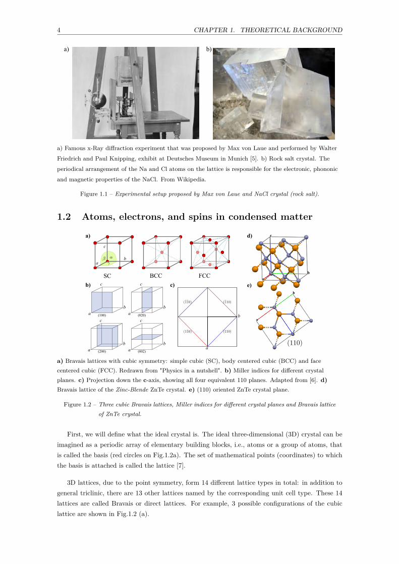
Back in 1912, M. Laue proposed a rather simple experiment (Fig.1.1a) and observed the X-Rayinterference due to the crystalline nature of a sample, for which he was awarded the Nobel Prizein 1914. One hundred years later, thanks to the progressively increasing knowledge and scientificinterest in the condensed matter physics, we developed some remarkable solid-state devices such astransistors, semiconductor lasers, optical fibers, lithium batteries, liquid crystal display, and manyothers.
Here, we introduce the baseline theory necessary for discussion of the following chapters. Thischapter will start with the notions about the arrangements and properties of atoms, electrons, andspins in solid matter. Next, the basics of the light-matter are explained with the definition of theelectromagnetic wave, optical properties of the material, and second-order nonlinear processes incrystals. At the end, a brief description of the temporal coupling of light with the electrons, atoms,and spins will be given.
3
4 CHAPTER 1. THEORETICAL BACKGROUND
a) Famous x-Ray diffraction experiment that was proposed by Max von Laue and performed by WalterFriedrich and Paul Knipping, exhibit at Deutsches Museum in Munich [5]. b) Rock salt crystal. Theperiodical arrangement of the Na and Cl atoms on the lattice is responsible for the electronic, phononicand magnetic properties of the NaCl. From Wikipedia.
Figure 1.1 – Experimental setup proposed by Max von Laue and NaCl crystal (rock salt).
1.2 Atoms, electrons, and spins in condensed matter
d)
e)
a) Bravais lattices with cubic symmetry: simple cubic (SC), body centered cubic (BCC) and facecentered cubic (FCC). Redrawn from "Physics in a nutshell". b) Miller indices for different crystalplanes. c) Projection down the c-axis, showing all four equivalent 110 planes. Adapted from [6]. d)Bravais lattice of the Zinc-Blende ZnTe crystal. e) (110) oriented ZnTe crystal plane.
Figure 1.2 – Three cubic Bravais lattices, Miller indices for different crystal planes and Bravais latticeof ZnTe crystal.
First, we will define what the ideal crystal is. The ideal three-dimensional (3D) crystal can beimagined as a periodic array of elementary building blocks, i.e., atoms or a group of atoms, thatis called the basis (red circles on Fig.1.2a). The set of mathematical points (coordinates) to whichthe basis is attached is called the lattice [7].
3D lattices, due to the point symmetry, form 14 different lattice types in total: in addition togeneral triclinic, there are 13 other lattices named by the corresponding unit cell type. These 14lattices are called Bravais or direct lattices. For example, 3 possible configurations of the cubiclattice are shown in Fig.1.2 (a).
5 CHAPTER 1. THEORETICAL BACKGROUND
The next important notation is the crystal plane orientation. The set of parallel planes thatintercept the crystal unit-cell can be noted as (hkl), where Miller’s indices h, k, and l define thepoint of intercept on the given crystal axes a, b, c at position 1/h, 1/k and 1/l respectively. Theexample of the crystal plane notation using Miller indices is shown in the Fig.1.2b. Usually, thereciprocal values of h, k, l are reduced to the set of integers with the least common multiplier. Ifplane cuts the axis on the negative side, the corresponding negative index is then noted as h, k, l,as seen from Fig.1.2c. The type of Bravais lattice combined with the crystal plane orientation canaffect the combination of the solid matter’s elastic, electronic, magnetic, and optical properties.
1.2.1 Ionic subsystem
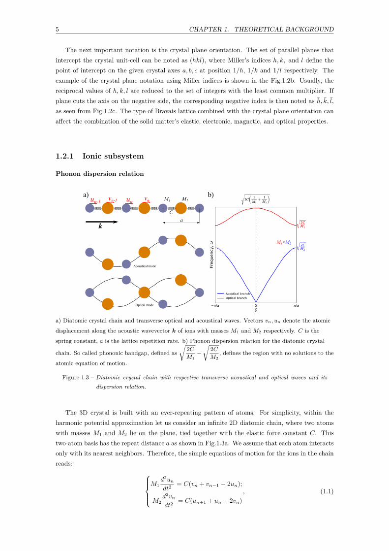
Phonon dispersion relation
a) Diatomic crystal chain and transverse optical and acoustical waves. Vectors vn, un denote the atomicdisplacement along the acoustic wavevector k of ions with masses M1 and M2 respectively. C is thespring constant, a is the lattice repetition rate. b) Phonon dispersion relation for the diatomic crystal
chain. So called phononic bandgap, defined as√
2CM1
−√
2CM2
, defines the region with no solutions to theatomic equation of motion.
Figure 1.3 – Diatomic crystal chain with respective transverse acoustical and optical waves and itsdispersion relation.
The 3D crystal is built with an ever-repeating pattern of atoms. For simplicity, within theharmonic potential approximation let us consider an infinite 2D diatomic chain, where two atomswith masses M1 and M2 lie on the plane, tied together with the elastic force constant C. Thistwo-atom basis has the repeat distance a as shown in Fig.1.3a. We assume that each atom interactsonly with its nearest neighbors. Therefore, the simple equations of motion for the ions in the chainreads:
M1d2un
dt2= C(vn + vn−1 − 2un);
M2d2vn
dt2= C(un+1 + un − 2vn)
, (1.1)

6 CHAPTER 1. THEORETICAL BACKGROUND
a) Phonon dispersion relation of a ZnTe crystal. Hollow symbols are experimental points, and lines aretheoretical calculations. From [8]. b) First Brillouin zone of the FCC lattice, with high-symmetry points.From Wikipedia.
Figure 1.4 – ZnTe phonon dispersion curve and first Brillouin zone of the FCC lattice.
and we will look for the nontrivial solutions in the form of the wave with respective amplitudesv and u:
un = ueinkae−iωt; vn = veinkae−iωt. (1.2)
Given the periodicity of this classical diatomic chain, we can apply the periodic boundary condition(Born-von Karman):
eikNa = 1, (1.3)
where N is the number of lattice repetitions, that defines the total chain length as L = Na.Solution of this boundary condition for k returns the value for the edges of the first Brillouin zone,containing all unique values of atomic vibrational frequency ω. If we substitute Eq.1.2 in Eq.1.1we find solutions for ω2:
ω2ac = C
M1M2
(M1 +M2 −
√M2
1 +M22 + 2M1M2 cos (ka)
);
ω2opt = C
M1M2
(M1 +M2 +
√M2
1 +M22 + 2M1M2 cos (ka)
).
(1.4)
These solutions tell us about the frequency range of the permitted oscillations of the crystal withinthe first Brillouin zone, called phonon dispersion curves are referred to as an acoustical and opticalbranch, and are shown in the Fig.1.3b. Within the acoustical branches, two atoms oscillate inthe same phase, following the similar pattern of the sound wave. For the optical branch, two ionsoscillate out of phase. Such vibration can be imagined as the action of electromagnetic (EM) waveson the two dipoles with opposite charges [7], hence the optical branch name. Optical and acoustical
branches are split by the amount of√
2CM1
−√
2CM2
at the edge of the Brillouin zone, defining therange of forbidden vibrational frequencies within the crystal, named phononic bandgap.
7 CHAPTER 1. THEORETICAL BACKGROUND
The example of the phonon dispersion curve of a ZnTe crystal is shown in Fig.1.4a. ZnTehas fcc lattice and is from F 43m [216] space group (Hermann–Mauguin notation), also known asZincblende. The 3 degrees of freedom (x, y, z) of each atom allow for 3p vibrational modes in total,where p is the number of atoms per unit cell. ZnTe phonon dispersion curves have 3 (1 Longitudinal(LA) and 2 Transverse (TA)) acoustical modes, where the remaining 3p − 3 will be reserved forLongitudinal (LO) and Transverse (TO) optical phonon branches. Along the strong symmetryaxes (ΓX, ΓL, see Fig.1.4b), due to the degeneracy of transverse branches, we can observe only4 modes: TA, TO, LA and LO. If we move perpendicularly to the (110) crystallographic plane,i.e., along [110] direction, TO and two TA branches lose that degeneracy, resulting in 3 × 2 = 6predicted vibrational modes in total.
Lattice heat capacity
The quanta of lattice vibrational energy is called a phonon. Energy of a given elastic mode,occupied by ns phonons (n phonons within the branch s) with frequency ωs and wave vector k
defined as:
ϵs = (ns + 1/2)ℏωs(k). (1.5)
Therefore, the total vibrational energy of the crystal could be simply expressed as the sum overall discrete energy values for all existing phonon normal modes:
Eph =∑s,k
(ns + 1
2
)ℏωs(k). (1.6)
Phonons are bosons. The mean number of phonons that occupy ns(k) energy state at giventemperature T can be approximated with Planck distribution:
⟨ns(k)⟩ = 1exp[ℏωs(k)
kBT
]− 1
, (1.7)
where kB is the Boltzmann constant. This distribution tells us that high-k states are more likelyto be occupied at higher temperatures. Knowing the thermal distribution of the phonon modes,we can write the generalized expression for the crystal vibrational energy density [9]:
Uph = Ueq + 12V
∑k,s
ℏωs(k) + 1V
∑k,s
⟨ns(k)⟩ ℏωs(k), (1.8)
where Ueq is the lattice energy at equilibrium (T = 0), and the second term corresponds to thezero-point vibration of the lattice mode s. The third term introduces the temperature dependenceof Uph. Finally, we can define the lattice heat capacity cL, at constant volume as:
cL =(∂Uph
∂T
)V
= 1V
∑k,s
∂
∂T⟨ns(k)⟩ ℏωs(k), (1.9)
8 CHAPTER 1. THEORETICAL BACKGROUND
showing the temperature dependence of cL. For given temperature range, there are differentapproximations for cL. For the majority of crystals at T > 300 K, one can use the law of Dulongand Petit (cL ∝ 3kBns/V ). At low temperatures Debye approximation (cL ∝ T 3) assumes thatonly low-ω acoustical modes are excited. This makes phonon frequency ωs directly proportionalto the wavevector k, resulting in a constant sound velocity. While Debye approximation works foracoustical branches, Einstein approximation is usually chosen as a first approximation to describethe energy contribution of optical phonons to cL. Both Debye and Einstein laws are designed towork within specific temperature range, and still, they both converge to the classic law of Dulongand Petit at high temperatures [7]. For the considerable number of the phonon modes, one canreplace the sum over k in the Eq.1.9 by an integral, saying that crystal has Ds(ω)dω modes in thefrequency interval [ω, ω + dω] and in the branch s:
cL = 1V
∑s
∫Ds(ω)dω ∂
∂T⟨ns(k)⟩ ℏωs((k), (1.10)
where Ds(ω) is the phonon density of states. In its general form, Ds(ω) ∝ 1vg
where vg is thephonon group velocity, also known as the speed of sound.
1.2.2 Electronic subsystem
When considering the electronic Hamiltonian with a constant potential (even zero by selectinga specific energy scale), the electron wave function becomes that of a free electrons’ Sommerfeldmodel with parabolic electron dispersion relation:
ϵ = ℏ2k2
2m , (1.11)
where m is the mass of the electron in vacuum. Adding some periodic boundary Born von Karmancondition, we obtain the quantization of the wave vector and the associated energy. The surfaceat a constant energy, plotted in the k space, defines the Fermi sphere.
In reality, the periodic arrangement of the lattice and its translational symmetry invariancehighly impact how the electron behaves inside the crystal. The electrons are indeed affected bythe periodic potential generated by neighboring electrons and lattice ions that leads to specificelectron-ions interaction, creating some "gaps" in the electronic band structure. The eigenfunctionof the electron, or Bloch wave, is written as the plane wave having periodicity defined by theBravais vectors R [9]. The electron wave functions become:
ψnb,k(r) = eik·runb,k(r), (1.12)
where k is the electron wave-vector, and nb is the so-called band index. The lattice periodicity isrepresented by the term unb,k(r) with the symmetry invariance:
unb,k(r + R) = unb,k(r), (1.13)
9 CHAPTER 1. THEORETICAL BACKGROUND
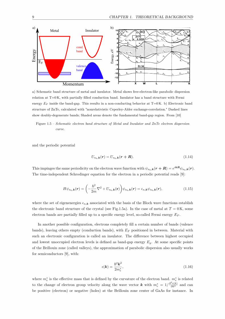
a) Schematic band structure of metal and insulator. Metal shows free-electron-like parabolic dispersionrelation at T=0 K, with partially filled conduction band. Insulator has a band structure with Fermienergy EF inside the band-gap. This results in a non-conducting behavior at T=0 K. b) Electronic bandstructure of ZnTe, calculated with "nonrelativistic Ceperley-Alder exchange-correlation." Dashed linesshow doubly-degenerate bands; Shaded areas denote the fundamental band-gap region. From [10]
Figure 1.5 – Schematic electron band structure of Metal and Insulator and ZnTe electron dispersioncurve.
and the periodic potential
Unb,k(r) = Unb,k(r + R). (1.14)
This impinges the same periodicity on the electron wave function with ψnb,k(r + R) = eikRψnb,k(r).The time-independent Schrodinger equation for the electron in a periodic potential reads [9]:
Hψnb,k(r) =(
− ℏ2
2m∇2 + Unb,k(r))ψnb,k(r) = ϵn,kψnb,k(r), (1.15)
where the set of eigenenergies ϵn,k associated with the basis of the Bloch wave functions establishthe electronic band structure of the crystal (see Fig.1.5a). In the case of metal at T = 0 K, someelectron bands are partially filled up to a specific energy level, so-called Fermi energy EF .
In another possible configuration, electrons completely fill a certain number of bands (valencebands), leaving others empty (conduction bands), with EF positioned in between. Material withsuch an electronic configuration is called an insulator. The difference between highest occupiedand lowest unoccupied electron levels is defined as band-gap energy Eg. At some specific pointsof the Brillouin zone (called valleys), the approximation of parabolic dispersion also usually worksfor semiconductors [9], with:
ϵ(k) = ℏ2k2
2m∗e
, (1.16)
where m∗e is the effective mass that is defined by the curvature of the electron band. m∗
e is relatedto the change of electron group velocity along the wave vector k with m∗
e = 1/∂2ϵ(k)∂k2 and can
be positive (electron) or negative (holes) at the Brillouin zone center of GaAs for instance. In
10 CHAPTER 1. THEORETICAL BACKGROUND
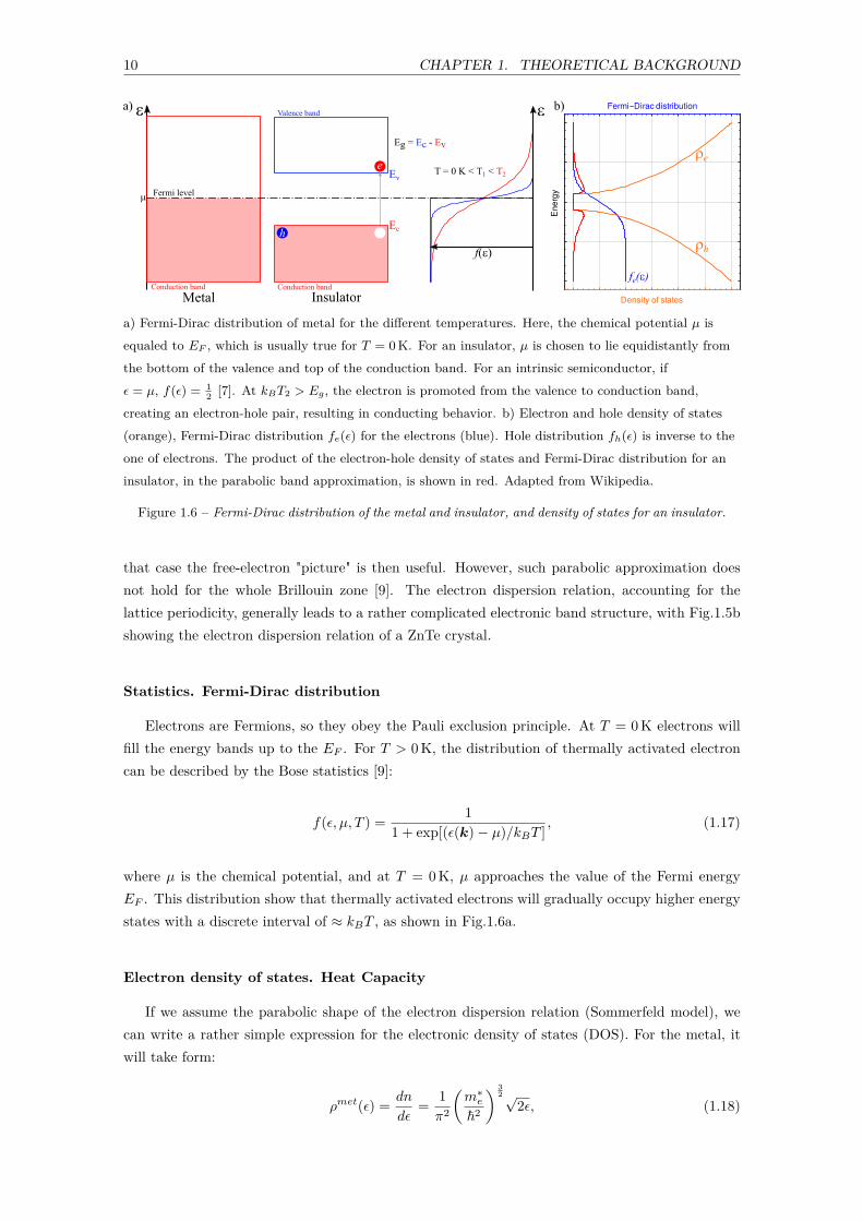
a) Fermi-Dirac distribution of metal for the different temperatures. Here, the chemical potential µ isequaled to EF , which is usually true for T = 0 K. For an insulator, µ is chosen to lie equidistantly fromthe bottom of the valence and top of the conduction band. For an intrinsic semiconductor, ifϵ = µ, f(ϵ) = 1
2 [7]. At kBT2 > Eg, the electron is promoted from the valence to conduction band,creating an electron-hole pair, resulting in conducting behavior. b) Electron and hole density of states(orange), Fermi-Dirac distribution fe(ϵ) for the electrons (blue). Hole distribution fh(ϵ) is inverse to theone of electrons. The product of the electron-hole density of states and Fermi-Dirac distribution for aninsulator, in the parabolic band approximation, is shown in red. Adapted from Wikipedia.
Figure 1.6 – Fermi-Dirac distribution of the metal and insulator, and density of states for an insulator.
that case the free-electron "picture" is then useful. However, such parabolic approximation doesnot hold for the whole Brillouin zone [9]. The electron dispersion relation, accounting for thelattice periodicity, generally leads to a rather complicated electronic band structure, with Fig.1.5bshowing the electron dispersion relation of a ZnTe crystal.
Statistics. Fermi-Dirac distribution
Electrons are Fermions, so they obey the Pauli exclusion principle. At T = 0 K electrons willfill the energy bands up to the EF . For T > 0 K, the distribution of thermally activated electroncan be described by the Bose statistics [9]:
f(ϵ, µ, T ) = 11 + exp[(ϵ(k) − µ)/kBT ] , (1.17)
where µ is the chemical potential, and at T = 0 K, µ approaches the value of the Fermi energyEF . This distribution show that thermally activated electrons will gradually occupy higher energystates with a discrete interval of ≈ kBT , as shown in Fig.1.6a.
Electron density of states. Heat Capacity
If we assume the parabolic shape of the electron dispersion relation (Sommerfeld model), wecan write a rather simple expression for the electronic density of states (DOS). For the metal, itwill take form:
ρmet(ϵ) = dn
dϵ= 1π2
(m∗
e
ℏ2
) 32 √
2ϵ, (1.18)
11 CHAPTER 1. THEORETICAL BACKGROUND
when for the semiconductor it will be:
ρsce (ϵ) = dn
dϵ= 1
2π2
(2m∗
e
ℏ2
) 32√
ϵ− Ec;
ρsch (ϵ) = dn
dϵ= 1
2π2
(2m∗
h
ℏ2
) 32√
Ev − ϵ; ,(1.19)
where m∗e and m∗
h are the effective mass of electron and hole, respectively; Ec is the energy ofthe top of conduction band, and Ev corresponds to energy at the top of the valence band. Inmetals, knowing the electron density of states, one can express the total electronic energy per unitof volume:
Ue =∫ ∞
0ϵρmet(ϵ)f(ϵ)dϵ. (1.20)
To get the electron energy density for an insulator, one needs to account for the electron andhole density of states and adjust the integration boundaries for these two contributions. Thetemperature dependent Fermi-Dirac distribution implies the temperature-dependent electron heatcapacity, defined as:
ce =(∂Ue
∂T
)V
. (1.21)
The electron heat capacity ce dominates the lattice heat capacity cL for metals at low temperaturesonly when EF ≫ kBT . A derivative of Eq.1.21 leads to the linear relation ce(Te) = λeT withelectron thermal conductivity λe = 96.6 J.mol−1.K−2 for copper for instance. For semiconductors,ce contribution to the heat capacity of the crystal dominates cL only in the high-temperatureregime, when EF ≪ kBT , although not many materials can support that.
Electrical conductivity in the semi-classical approach
Let us picture the Fermi surface of a crystal centered at the origin of k space, as shown inFig1.7a. In the ground state, the net electron momentum (mev = ℏk) is zero, since for everyelectron orbital at kx,y there is an occupied opposite electron state at −kx,y. In the presence ofan external electric force F = −eE acting on these electrons, the second law of motion reads:
− eEx = ℏdkx
dt= me
dvx
dt. (1.22)
Over time t, each electron will experience the equivalent displacement in k-space, as shown inFig.1.7b, and the total shift of the Fermi surface could be written as:
δkx = −eExt
ℏ. (1.23)
After the electric field is lifted, the electrons will return to equilibrium. The electron momentum,gained in the presence of Ex can be dissipated via collisions with phonons, lattice imperfections andimpurities. We can define the characteristic time t = τe during which the electrons will maintain
12 CHAPTER 1. THEORETICAL BACKGROUND
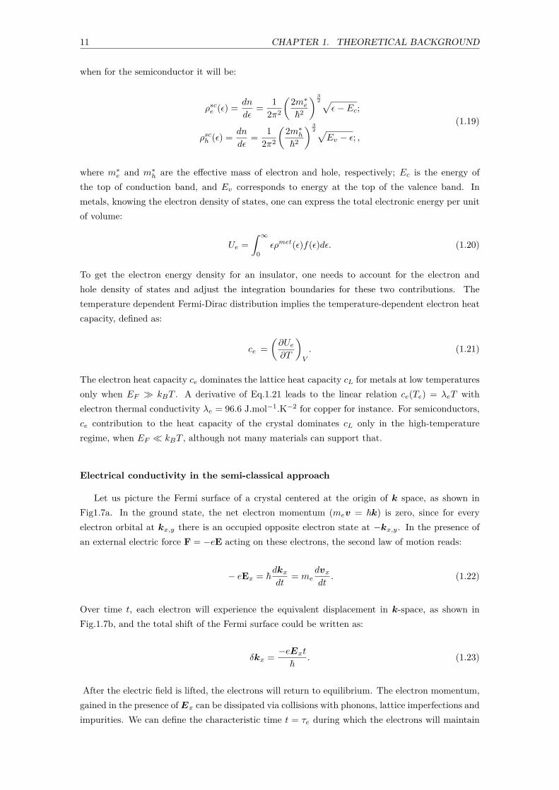
kx
ky
kx
kyE
kxa) b)
Circular Fermi surface of a 2D metal, with dots being the occupied free-electron states. a) Withoutapplied field E the net momentum zero, since for each electron state (kx, ky) there is an electron at(−kx,−ky). b)With −eEx force applied on the electrons, Fermi surface will be shifted (red circle) fromits initial position (dotted circle), gaining the increase of electron momentum δpx = δkx
Figure 1.7 – Shift of the circular Fermi surface under the presence of the electric field.
the δkx shift of the Fermi surface. Therefore, the density of electric current generated under theaction of Ex is [7]:
j = −envx = e2nτe
meEx = σEx, (1.24)
which is the definition of microscopic Ohm’s law, with σ being the conductivity of the metal andτe is electron scattering time. For the conductivity of the semiconductor, one needs to account forthe contribution of both electrons and holes:
σsc = e2nτe
me+ e2hτh
mh, (1.25)
where τe and τh are the electron and hole collision time, respectively.
We then can explore the total amount of kinetic energy gained by the conduction electrons.With change of electron momentum ℏδkx, change in kinetic energy per unit volume is:
δUk = n(ℏδkx)2
2me= 1
2me
e2nj2 = 1
2τej2
σ. (1.26)
The total density of absorbed energy by the electron subsystem will then read as:
Wk = ∂Uk
∂t= 1
2j2σ−1 = 12j2ρ, (1.27)
with resistivity ρ = σ−1. This is a microscopic analogy of the well-known Joule heating process,saying that the electrical current generated by the motion of the charge, and it will contribute tothe increase of the internal energy of the crystal.
13 CHAPTER 1. THEORETICAL BACKGROUND
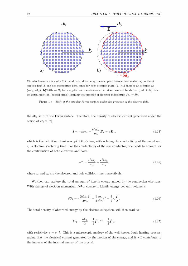
a) Depiction of atomic orbitals in molecules and solids. The principal quantum number n identifieselectron shell when electrons with the identical orbital quantum number l from the subshell. The wayelectrons fill in shell and subshell levels is indicated by the arrows above. For example, because of thelower energy state, the 4s orbital fills before the 3d. Image is taken from Encyclopedia Britannica. b) (1)Classical view of the spin-orbit interaction. E generated by the nucleus in the rest frame of movingelectron will transform into magnetic field Bso, interacting with electron spin. (2) LS coupling of orbitaland spin angular momenta for atoms with Z < 10.
Figure 1.8 – Sketch of electronic states in an atom and electron spin-orbit interaction.
Another important value related to the electron scattering time τe is the distance electronstraveled between the collisions, namely the electron mean-free path:
Λ = vxτe. (1.28)
Usually, the electron velocity vx is defined in terms of Fermi velocity vF , which accounts for thecurvature of the electron dispersion band. However, in the case of free-electron gas approximation,the average thermal electron velocity
⟨v2
th
⟩is proportional to the increase of system kinetic energy
by amount 32kBT/me.
1.2.3 Spin subsystem
The electron state in an atom can be described with 4 quantum numbers: principal quantumnumber n, orbital quantum number l, magnetic quantum number ml, and spin quantum numberms. Electrons with the same n form an electron shell, and the principal quantum number can takeinteger values from 1 to 7. Orbital quantum number l defines an electron subshell within electronshell n, having n possible values from 0 to (n − 1), as shown in Fig.1.8a. Hund’s rules describethe population of electron shells and subshells. l defines electron orbital within a subshell, and ml
gives a projection of the orbital angular momentum l on the given axis. Values of ml are integersin the range [−l; l]. ms gives the axis projection of intrinsic electron angular momentum, calledspin s. For an electron, ms can take the fixed values of ±1/2, when two orientations of s along the

14 CHAPTER 1. THEORETICAL BACKGROUND
given axis are referred to as spin-up and spin-down. In quantum mechanics, components of spinangular momentum operator s obey the following commutation relation [11]:
[si, sj ] = iℏϵijksk, (1.29)
with ϵijk being Levi-Civita permutation symbol. This permutation relation holds for orbital an-gular momentum operator l as well. The eigenvalues of s are ±ℏ/2. Two commuting operatorssz and s2 have respective eigenvalues of ±ℏs and ℏ2s(s + 1). Electrons’ orbital motion and spinassociated with respective orbital µorb and spin µs magnetic moment operators as:
µorb = −µB
ℏl; µs = −µBgs
ℏs, (1.30)
where µB = |e|ℏ/2me is Bohr magneton with e being elementary charge and gs is the Landé’s g-factor. The electron total angular momentum operator j (Fig.1.8b2), and hence the total magneticmoment operator are defined as:
j = s + l; µe = µs + µl. (1.31)
The first existence of the electron spin was confirmed experimentally by Stern and Gerlach [12]in 1922, although the result of their experiment was misinterpreted. Researchers theoreticallyintroduced the intrinsic magnetic moment of the electron 6 years after Stern’s experiment as theconsequence of the relativistic corrections [13].
Spin-orbit interaction
In 1928 Dirac published the paper on the quantum mechanics, where he derived the relativisticversion of the Schrödinger equation, and introduced the spin-operators [14]. The relativistic single-electron Dirac Hamiltonian in the symmetric potential, under the static magnetic field B
tot, wasderived as [13]:
H = T + Trel + HC + HD + HSO + HZ , (1.32)
The first two terms in Eq.1.32 are non-relativistic T and relativistic Trel corrections to the electron’skinetic energy. The next two terms are the potential energy of the electron in the nucleus potential,i.e., Coulomb force HC , and the so-called Darwin term HD, arising from the relativistic fluctuationsof the electron’s potential energy. Interestingly, in the Dirac representation, the wave functionsassociated with H are called spinors, and compared to vectors, they transform differently underrotation in 3D space [13].
The fifth term, HSO, describes the electron spin-orbit interaction, which helped explain thedoublets in the hydrogen spectrum observed by Michelson back in 1892 [15]. One can approachthe spin-orbit coupling term from the rest frame of the moving electron. The orbital motion ofthe nucleus around the stationary electron is equivalent to the current loop that will generatemagnetic field BSO ∝ E × ve/c
2 (Fig.1.8b1). This magnetic field will affect the electron spin
15 CHAPTER 1. THEORETICAL BACKGROUND
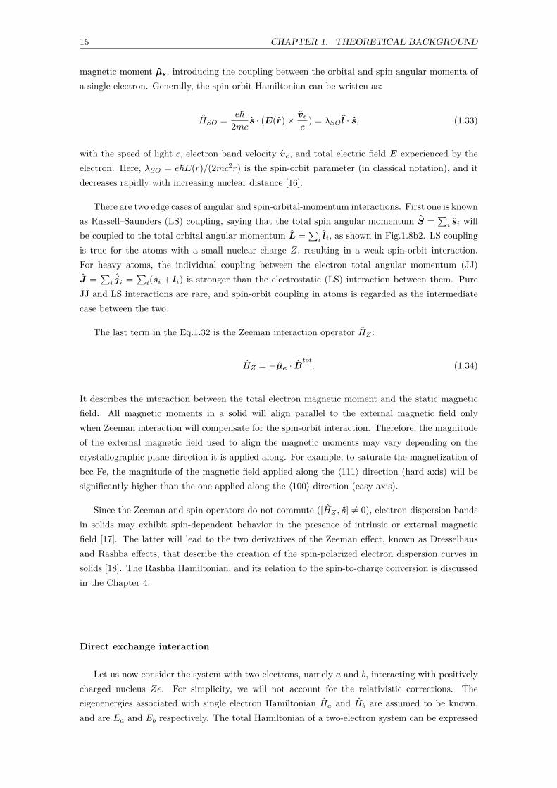
magnetic moment µs, introducing the coupling between the orbital and spin angular momenta ofa single electron. Generally, the spin-orbit Hamiltonian can be written as:
HSO = eℏ2mc s · (E(r) × ve
c) = λSO l · s, (1.33)
with the speed of light c, electron band velocity ve, and total electric field E experienced by theelectron. Here, λSO = eℏE(r)/(2mc2r) is the spin-orbit parameter (in classical notation), and itdecreases rapidly with increasing nuclear distance [16].
There are two edge cases of angular and spin-orbital-momentum interactions. First one is knownas Russell–Saunders (LS) coupling, saying that the total spin angular momentum S =
∑i si will
be coupled to the total orbital angular momentum L =∑
i li, as shown in Fig.1.8b2. LS couplingis true for the atoms with a small nuclear charge Z, resulting in a weak spin-orbit interaction.For heavy atoms, the individual coupling between the electron total angular momentum (JJ)J =
∑i ji =
∑i(si + li) is stronger than the electrostatic (LS) interaction between them. Pure
JJ and LS interactions are rare, and spin-orbit coupling in atoms is regarded as the intermediatecase between the two.
The last term in the Eq.1.32 is the Zeeman interaction operator HZ :
HZ = −µe · Btot. (1.34)
It describes the interaction between the total electron magnetic moment and the static magneticfield. All magnetic moments in a solid will align parallel to the external magnetic field onlywhen Zeeman interaction will compensate for the spin-orbit interaction. Therefore, the magnitudeof the external magnetic field used to align the magnetic moments may vary depending on thecrystallographic plane direction it is applied along. For example, to saturate the magnetization ofbcc Fe, the magnitude of the magnetic field applied along the ⟨111⟩ direction (hard axis) will besignificantly higher than the one applied along the ⟨100⟩ direction (easy axis).
Since the Zeeman and spin operators do not commute ([HZ , s] = 0), electron dispersion bandsin solids may exhibit spin-dependent behavior in the presence of intrinsic or external magneticfield [17]. The latter will lead to the two derivatives of the Zeeman effect, known as Dresselhausand Rashba effects, that describe the creation of the spin-polarized electron dispersion curves insolids [18]. The Rashba Hamiltonian, and its relation to the spin-to-charge conversion is discussedin the Chapter 4.
Direct exchange interaction
Let us now consider the system with two electrons, namely a and b, interacting with positivelycharged nucleus Ze. For simplicity, we will not account for the relativistic corrections. Theeigenenergies associated with single electron Hamiltonian Ha and Hb are assumed to be known,and are Ea and Eb respectively. The total Hamiltonian of a two-electron system can be expressed
16 CHAPTER 1. THEORETICAL BACKGROUND
in a simple form:
Hab = Ha(r1) + Hb(r2) + e2
4πϵ0|r1 − r2|, (1.35)
where the third term is the perturbation due to electron-electron interaction. Since we neglectedspin-orbit interaction, the electron wave function can be factorized in orbital Φi(rj) and spin Ωi(sj)parts [17]. For such a system of two fermions, due to the Pauli exclusion principle, each particlecan be either spin up or down, resulting a total combination of four basis states of the spin-partwave function Ωi(sj): three Symmetric triplets:
|↑, ↑⟩
(|↑, ↓⟩ + |↑, ↓⟩)/√
2
|↓, ↓⟩
S = 1ℏ ; (1.36)
and one Asymmetric singlet:
(|↑, ↓⟩ − |↑, ↓⟩)/√
2 ; S = 0, (1.37)
where S denotes the total spin of the basis state. When the electron-electron interaction is smallcompared to the Ea and Eb, it is assumed that there is no coupling of the orbital states. If aset of orbital-part electron wave functions form an orthonormal basis, it is possible to derive theeigenenergies of a singlet Es and triplet Et states [13]
Es = Ea + Eb +Kab + Jab;
Et = Ea + Eb +Kab − Jab,(1.38)
that are split by the amount of 2Jab. Here, the
Kab =∫ ∫
dr1dr2|Φa(r1)|2|Φb(r2)|2 (1.39)
is the quantitative measure of the overlap between two electron orbitals and is called the overlapintegral. Jab is an analogy of two-site Coulomb interaction and is called the interaction integral:
Jab =∫ ∫
dr1dr2Φ∗a(r1)Φ∗
b(r2) e2
4πϵ0r12Φb(r1)Φa(r2). (1.40)
Paul Dirac derived the eigenenergies from Eq.1.38 by introducing the spin-dependent term in theHamiltonian instead of two-electron Coulomb exchange, as demonstrated above. The so-calledDirac exchange Hamiltonian Hex for the two-electron system is:
Hex = 14(Es + Et) − 1
4(Es − Et)s1 · s2/ℏ2, (1.41)
17 CHAPTER 1. THEORETICAL BACKGROUND
where the terms in parenthesis correspond to the energy of bonding 2(Es − Et) and antibonding(Es +Et) orbitals. This equation says that the exchange interaction is a purely electrostatic effectthat arises from the spin-spin interaction and Pauli exclusion principle. For N -electron system,the exchange interaction Hamiltonian is known as the Heisenberg Hamiltonian:
Hex = −2N∑
i<j
Jexij si · sj/ℏ2, (1.42)
where the exchange integral Jexij has the same form as Jab. When the exchange integral Jex
ij ispositive, according to Eq.1.38, adjacent spins point in the same direction, i.e., aligned in parallel,which is the sign of ferromagnetic coupling. Inversely, if Jex
ij is negative, consecutive spins pointin the opposite direction, resulting in antiferromagnetic interaction. If more than one magneticsubstrate with an antiparallel spin orientation do not cancel each other, ferrimagnetic ordering canoccur [16].
The magnitude of the exchange integral Jexij is determined by the overlap integral Kij (see
Kab in Eq.1.39). If the wave functions of the participating electrons do not overlap, there will beno spontaneous spin ordering. When the distance between two magnetic ions is large, meaningthat the direct exchange not possible, the spin-spin exchange mechanism can be mediated bysuperexchange (via oxygen orbitals in oxides, for instance) [17].
Ferromagnetism. Stoner model
The direct exchange interaction in solids can result in spontaneous spin ordering, giving rise tothe macroscopic magnetization M defined as:
M = 1V
∑i
⟨µi⟩, (1.43)
where ⟨µi⟩ is the expected value of the total magnetic moment operator (see Eq.1.31).
Measurement of the spontaneous magnetization in Fe, Co, and Ni revealed that the magneticmoment per atom is not indeed an integer multiple of Bohr magneton, contradicting the existingat that time theory. This problem was solved by Mott [19], Slater [20], and Stoner [21] around the1940s. As an example, the Stoner band model was developed to explain broken µB numbers as aresult of ferromagnetism .
The classical Stoner model is used to predict spontaneous ferromagnetic ordering in solids, andit assumes separate band structures for spin-up and spin-down electron states. Since it is alwayshard to keep track of the true sample magnetization, we can apply a static external magnetic field(Bext) to align the magnetization of the sample parallel to the applied field, as shown in Fig.1.9a.Since spin magnetic moment and electron spin have opposite directions (see Eq.1.30), the stateswith larger electron population (majority band) will be aligned in the opposite direction to Bext,while ones having a smaller population (minority band) will be parallel to the applied magneticfield. Hence, the magnetization and the spin minority will always point in the direction of Bext.
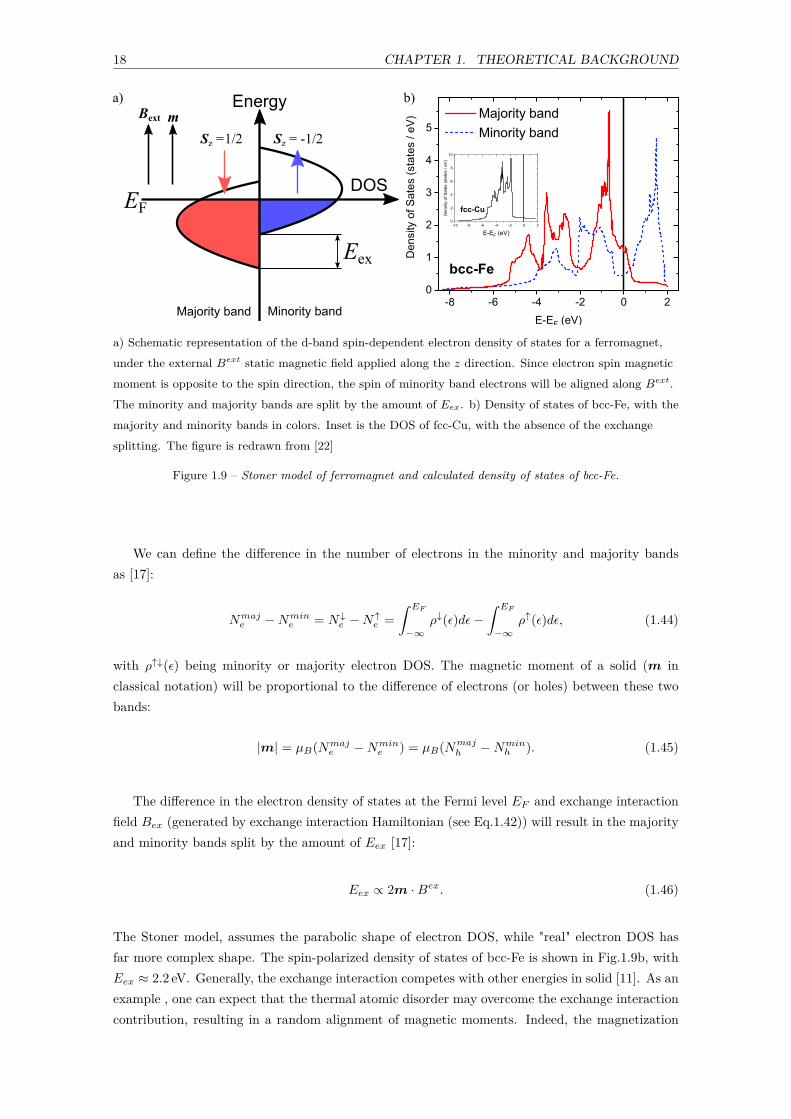
18 CHAPTER 1. THEORETICAL BACKGROUND
a) Schematic representation of the d-band spin-dependent electron density of states for a ferromagnet,under the external Bext static magnetic field applied along the z direction. Since electron spin magneticmoment is opposite to the spin direction, the spin of minority band electrons will be aligned along Bext.The minority and majority bands are split by the amount of Eex. b) Density of states of bcc-Fe, with themajority and minority bands in colors. Inset is the DOS of fcc-Cu, with the absence of the exchangesplitting. The figure is redrawn from [22]
Figure 1.9 – Stoner model of ferromagnet and calculated density of states of bcc-Fe.
We can define the difference in the number of electrons in the minority and majority bandsas [17]:
Nmaje −Nmin
e = N↓e −N↑
e =∫ EF
−∞ρ↓(ϵ)dϵ−
∫ EF
−∞ρ↑(ϵ)dϵ, (1.44)
with ρ↑↓(ϵ) being minority or majority electron DOS. The magnetic moment of a solid (m inclassical notation) will be proportional to the difference of electrons (or holes) between these twobands:
|m| = µB(Nmaje −Nmin
e ) = µB(Nmajh −Nmin
h ). (1.45)
The difference in the electron density of states at the Fermi level EF and exchange interactionfield Bex (generated by exchange interaction Hamiltonian (see Eq.1.42)) will result in the majorityand minority bands split by the amount of Eex [17]:
Eex ∝ 2m ·Bex. (1.46)
The Stoner model, assumes the parabolic shape of electron DOS, while "real" electron DOS hasfar more complex shape. The spin-polarized density of states of bcc-Fe is shown in Fig.1.9b, withEex ≈ 2.2 eV. Generally, the exchange interaction competes with other energies in solid [11]. As anexample , one can expect that the thermal atomic disorder may overcome the exchange interactioncontribution, resulting in a random alignment of magnetic moments. Indeed, the magnetization
19 CHAPTER 1. THEORETICAL BACKGROUND
M is proportional to [17]:
M ∝ (Tcrit − T )α, (1.47)
where Tcrit is the critical temperature (Curie or Neel temperature for ferro- and antiferromagnets,respectively) above which the magnetic order vanishes, and α is the critical exponent that differswith the material.
Magnons
Ferromagnetic metal in the ground state at T = 0 K, according to Eq.1.38, prefers to haveits spins aligned in parallel, which leads to the lowest possible energy state. If we treat spins asclassical vectors, the total exchange energy in this ground state will be equal to −2NJexs2 withN being the number of neighbors. Thus, we can estimate the thermal energy (Eq.1.47) requiredto eliminate the spontaneous ground-state magnetization as [11]:
kBTC = −2NJexs2
ℏ2 . (1.48)
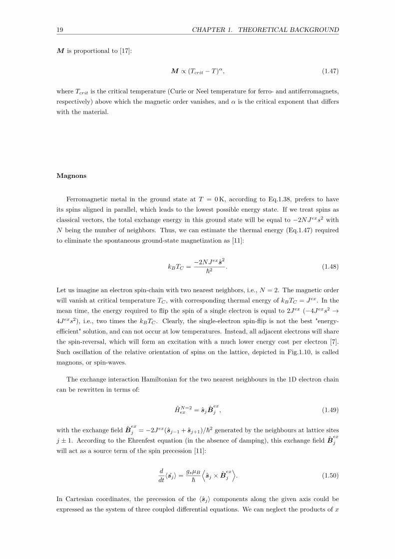
Let us imagine an electron spin-chain with two nearest neighbors, i.e., N = 2. The magnetic orderwill vanish at critical temperature TC , with corresponding thermal energy of kBTC = Jex. In themean time, the energy required to flip the spin of a single electron is equal to 2Jex (−4Jexs2 →4Jexs2), i.e., two times the kBTC . Clearly, the single-electron spin-flip is not the best "energy-efficient" solution, and can not occur at low temperatures. Instead, all adjacent electrons will sharethe spin-reversal, which will form an excitation with a much lower energy cost per electron [7].Such oscillation of the relative orientation of spins on the lattice, depicted in Fig.1.10, is calledmagnons, or spin-waves.
The exchange interaction Hamiltonian for the two nearest neighbours in the 1D electron chaincan be rewritten in terms of:
HN=2ex = sjB
ex
j , (1.49)
with the exchange field Bex
j = −2Jex(sj−1 + sj+1)/ℏ2 generated by the neighbours at lattice sitesj ± 1. According to the Ehrenfest equation (in the absence of damping), this exchange field B
ex
j
will act as a source term of the spin precession [11]:
d
dt⟨sj⟩ = gsµB
ℏ
⟨sj × B
ex
j
⟩. (1.50)
In Cartesian coordinates, the precession of the ⟨sj⟩ components along the given axis could beexpressed as the system of three coupled differential equations. We can neglect the products of x
20 CHAPTER 1. THEORETICAL BACKGROUND
Perspective and an aerial view of spins on a lattice with lattice constant a. Spin wave in aerial view isdrawn through the end of the spin vectors. The image was redrawn from [7]
Figure 1.10 – Spin wave on the 1D chain of spins.
and y components, since the expected values of sx,yj ≪ sz
j [16]:
d
dtsx
j = −JexgµB
ℏ(2sy
j − syj−1 − sy
j+1)
d
dtsy
j = −JexgµB
ℏ(2sx
j − sxj−1 − sx
j+1)
d
dtsz
j = 0
(1.51)
We will look for the solutions in the form of traveling wave ∝ exp[ikja−ωmt], with lattice constanta. The solution for the precession with a frequency ωm defines the magnon dispersion relation [7]:
ℏωm = −4JexS(1 − cos(ka)). (1.52)
The magnon dispersion relation for ka ≪ 1 has the form ℏωm = DSW k2, with stiffness parameterDSW = 2JexSa2. Magnons are bosons, and the quantized energy of a magnon is defined as:
ϵm =(nm + 1
2
)ℏωm, (1.53)
where nm is the number of magnons in the mode with frequency ωm at the zone center [11]. ForT < Tcrit magnons behave like bosons, so they follow the Bose statistics. Interestingly, the magnonsare in some way similar to phonons. Instead of the relative precession of an atomic position on alattice, spin waves are oscillations of the relative orientation of the lattice spin magnetic moments.
The magnon contribution to the heat capacity of the solid can be expressed in terms of thespin-correlation function ⟨si · sj⟩ (see Eq.1.42) [11]:
cm = −2NZJex ∂⟨si · sj⟩∂T
(1.54)
1.3 Light-matter interaction
1.3.1 Optical properties and dielectric function
Most optical phenomena can be explained with the classical electromagnetic (EM) approach,from the perspective of the physical interaction between charged particles. The light propagation

21 CHAPTER 1. THEORETICAL BACKGROUND
inside the material can be described by Maxwell’s equations:
∇ · D = ρ, ∇ · B = 0, ∇ × E = −∂B
∂t, ∇ × H = j + ∂D
∂t, (1.55)
where D is electric flux density, E is electric field strength, B and H are magnetic flux andmagnetic field respectively, ρ is charge density and j is electric current density (free carriers). Inthe linear regime, when the material is not charged, homogeneous, and isotropic the following setof equations can be established:
ρ = 0, j = σE, D = ε0εE, B = µ0H, (1.56)
where σ is conductivity, ε0 is electric constant, µ0 is magnetic constant and ε is the medium per-mittivity. Therefore, using Eq.1.55 one can derive the generalized wave equation for the dielectricsystem:
∇2E − ε
µ0ε0
∂2E∂t2
= µ0∂j
∂t, which gives:
k2E = ω2µ0εE + iµ0ωσE.
(1.57)
By noting that speed of light is c = 1√ε0µ0
and dielectric constant of the material is ε = ε0εb,the wave vector expressed in terms of light frequency ω as:
k = ω
c
√εb + iσ
ε0ω= k′ + ik′′, (1.58)
with εb and iσ/ε0ω are the bound and free electron contributions to the relative dielectric constant,with k′ and k′′ being the real and imaginary parts of the complex wavevector, respectively. Wethen can rewrite k as:
k = ω
cn(ω) (1.59)
where n(ω) = n(ω)+iK(ω) is complex index of refraction, with refractive index n(ω) and extinctioncoefficient K(ω). With the extinction coefficient K(ω) one can estimate the EM wave intensityI(z) 1 attenuation in medium along the z-direction. From the Beer-Lambert law we obtain:
I(z) = I0 exp(−αz), (1.60)
with α = 2ωK/c = 4πK/λ is the absorption coefficient (λ is the light wavelength). The absorptionof EM has an exponential profile for K = 0, while K = 0 defines lossless transmission.
1. I(z) ∝ |E0 exp(Kz)|2

22 CHAPTER 1. THEORETICAL BACKGROUND
The well-known relation between n(ω), electric susceptibility χ(ω) and complex permittivityε(ω) of the material written as:
ε(ω) = 1 + χ(ω) = n2(ω) = ε1(ω) + iε2(ω), (1.61)
where ε1(ω) is real and ε2(ω) is the imaginary part of the frequency dependent dielectric constant.In a crystal, light-matter interaction depends on the crystal symmetry and light propagation direc-tion with respect to the crystallographic plane orientation, resulting ε, χ(ω) and n being tensors.In this section, for simplicity, we will assume that our solids are isotropic, lifting the tensor notationfor all the optical constants discussed below.
Drude and Lorentz Model: semi-classical approach
The electron degrees of freedom within partially filled electron bands and interband transi-tions play an important role in the optical properties of both metals and semiconductors. In thissubsection, we address the intraband Drude and interband Lorentz contributions to the dielectricfunction ε.
In the Section 1.2.2 we defined the electrical conductivity σ of a metal and introduced theaverage phenomenological electron and hole relaxation time τe. Now, we want to explore theaction of EM field E(t) = E0(exp[−iωt]) on nearly-free conduction-band electrons. The classicaldamped equation of motion, describing the change in electron position r in time is written as:
me
(d2r
dt2+ 1τe
dr
dt
)= −eE(t). (1.62)
We can express the single-electron dipolar moment as p = er. Then, the macroscopic polarizationP created by the displacement of the electron cloud reads [23]:
P = nr = ε0χ(ω)E(t). (1.63)
Combining the two previous equations, we can deduce the free-electron contribution to the electricsusceptibility of the crystal. The so-called Drude susceptibility is:
χD(ω) = − ne2
ε0me
1ω2 + iω/τe
= −ω2
p
ω2 + iω/τe, (1.64)
with
ωp =
√ne2
ε0me(1.65)
being the plasma frequency, where τe is the electron scattering time . The electron scattering rateinvolves multiple mechanisms, and highly depends on the electron temperature. Different scatteringmechanisms involve carriers energy loss via coupling with the phonons, defects, impurities, surfaces
23 CHAPTER 1. THEORETICAL BACKGROUND
and with other carriers [24]. From Eq.1.61, we can write the Drude dielectric constant as:
εD(ω) = 1 −ω2
p
ω2 + iω/τe. (1.66)
This equation tells that the optical properties within the Drude model solely depend on the plasmafrequency and τe. Hence, we can establish 3 fundamentally different regimes of light-matter inter-action in metals, depicted in Fig.1.11a:
1. ωτe ≪ 1: Hagen-Rubens regime, where optical properties mainly defined by the DC conduc-tivity (see Eq.1.24), rendering εD
1 frequency-independent;
2. 1/τe < ω < ωp: Relaxation regime, defining the range of frequency-independent light reflec-tivity
3. ωp < ω: Transparent regime, where the metal becomes transparent, with a monotonousdecrease of εD
1 and εD2 .
For the semiconductor, the complex dielectric function can be derived from a Lorentz model ofthe bounded electrons:
me
(d2r
dt2+ 1τ
dr
dt+ ω2
0,nr
)= −eE(t), (1.67)
that differs from the Drude model only by an additional restoring force term, which correspondsto the interband transition. This model does not lead to well-defined energy gaps, but it is widelyused to describe non-conducting materials [25]. The derived Lorentz complex dielectric function,for multiple electron transitions reads:
εL(ω) = 1 +∑
n
ω2p,n(
ω20,n − ω2
)+ iω/τn
, (1.68)
where ωp,n denotes the characteristic frequency associated to the electronic population of the leveln, τn is the phenomenological damping time, defining the width of the Lorentz oscillator and ω0,n
is the resonant frequency of the n-th type electron interband transition. Interestingly, the classicalLorentz model is really close to its quantum counterpart [24]:
εL(ω) = 1 +∑
n
fnω2p,n
(ω2j − ω2) + iω/τn
, (1.69)
with oscillator strength defined as:
fj = 2m∗e
ℏ2 ℏωn|rn|2, (1.70)
where rn is the displacement of the n-th electron. The simple Lorentz model, with only oneoscillator (see Eq.1.68) has 4 distinct spectral regimes:
1. ω < (ω0 − 1/τ): Low frequency range, where εL2 is infinitely small, resulting little to no
absorption (ℏω < Eg);
2. ω ≈ ω0: Absorption range, where electrons can be excited across the bandgap;
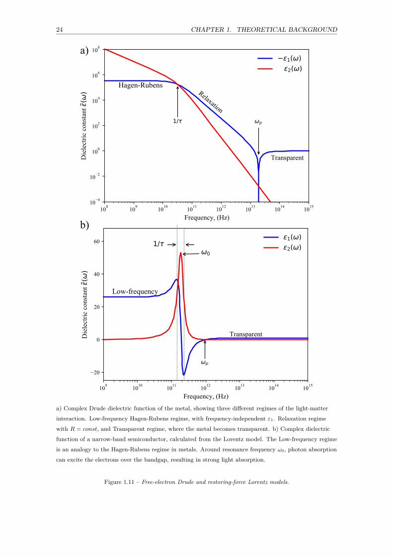
24 CHAPTER 1. THEORETICAL BACKGROUND
a) Complex Drude dielectric function of the metal, showing three different regimes of the light-matterinteraction. Low-frequency Hagen-Rubens regime, with frequency-independent ε1. Relaxation regimewith R = const, and Transparent regime, where the metal becomes transparent. b) Complex dielectricfunction of a narrow-band semiconductor, calculated from the Lorentz model. The Low-frequency regimeis an analogy to the Hagen-Rubens regime in metals. Around resonance frequency ω0, photon absorptioncan excite the electrons over the bandgap, resulting in strong light absorption.
Figure 1.11 – Free-electron Drude and restoring-force Lorentz models.
25 CHAPTER 1. THEORETICAL BACKGROUND
3. (ω + 0 − 1/τ) < ω < ωn: Reflection range, analogy of Drude relaxation regime;
4. ω > ωn: Transparent regime, where reflectivity drops to zero, rendering material transparent.
Metals. Interband contribution
The Drude model shows good agreement with the experimental data in the low-frequency range,rapidly diverging from the experiment at higher frequencies. The reason is that the Drude modeldoes not take into account the band structure of the metal. For the real 3D metal, the absorptionof a photon with sufficiently high energy can provoke an interband transition of the electron fromthe valence band to the conduction band above the EF . For example, we can separate the boundand free-electron contributions and account for possible interband transitions by introducing aLorentz term into the Drude model. The combined Drude-Lorentz model gives:
εDL(ω) = 1 −ω2
p
ω2 + iω/τe+
n=k∑n=1
ω2p,n
(ω20,n − ω2) + iω/τn
, (1.71)
for k is the number for all allowed interband transitions. As seen from Fig.1.12a, the compositeDrude-Lorentz model (with n = 1) slightly extends the prediction range of ε(ω). Even whenaccounting only for one Lorentz term, we still can estimate the energy of an interband transitionthreshold of Au (ℏωIB ≈ 2.7 eV), which is not so far from the real value of 2.4 eV. In a moregeneral form, the dielectric constant of the metal is written as a function of both interband andintraband contributions as:
ε(ω) = 1 + χD(ω) + χIB(ω), (1.72)
where χIB(ω) is interband electric susceptibility that accounts for all possible interband transitions.Interband transitions in metals can not be neglected in the high-frequency range and play animportant role in the optical properties of metals. The optical frequencies above the interbandtransition threshold ℏωIB will be highly absorbed. For example in Au, light with wavelengthsbelow 520 nm will be strongly absorbed, translating to its "yellowish" color.
The excitation of an electron above the Fermi level will leave a vacancy at the electrons’ initialposition, known as a hole. Electron-hole pair excitation (due to intraband or interband absorption)must satisfy the law of momentum conservation:
k = k′ + K, (1.73)
where k and k′ are the electron and hole wave vectors, and K is reciprocal lattice vector. Themomentum conservation can be fulfilled with two- or three-particle interactions.
The electron can absorb the photon if the photon energy corresponds to the energy differencebetween the hole and electron state:
ℏω = ϵ(k) − ϵ(k′), (1.74)

26 CHAPTER 1. THEORETICAL BACKGROUND
a) Comparison between the intraband Drude and composite Drude-Lorentz contributions to the realε1(ω) and imaginary ε2(ω) parts of the experimental dielectric function of gold. Inset: Interbandcontribution, defined as the difference between experimental data and intraband Drude model to the realand imaginary parts of the Au’s dielectric function. Experimental data are taken from [26]. b)Representation of the three possible electron transitions in metals and insulators. Direct interbandabsorption, mediated by the electron-photon interaction. Indirect intraband or interband transitions,followed by the phonon emission, are required due to the momentum conservation law.
Figure 1.12 – Intraband and interband contributions to complex dielectric function of gold and schemaof allowed transitions in metals and semiconductors.
which defines the direct optical (or vertical) electron transition. In addition, the momentumconservation can be fulfilled by the emission/absorption of a third particle, for example, a phonon.In this case, the momentum conservation law reads:
ℏω = ϵ(k) − ϵ(k′) ± ℏωph, (1.75)
where ωph is the frequency of emitted phonon. Normally, the direct optical transition requires thelowest amount of energy, and most of the time, it will be dominant during photon absorption.
Calculation of an interband contribution
The interband contribution to the dielectric constant can be calculated using the so-called Roseimodel [27–29]. This model takes into account the effective masses of the electrons in the parabolicband structure of noble metals in different directions relative to the Γ point. If we consider thephoton with energy ℏω that stimulates the transition from initial i to final f band, we can write:
ϵf (k) = ℏω + ϵi(k), (1.76)
with energies ϵf , ϵi in final and initial electron bands, respectively. With respect to [28, 30], wecan write the joint density of states Ji→j as:
Ji→j(ℏω) =∫Di→j(ϵ, ℏω)[1 − f(ϵ+ ℏω, µ, T )]dϵ, (1.77)
27 CHAPTER 1. THEORETICAL BACKGROUND
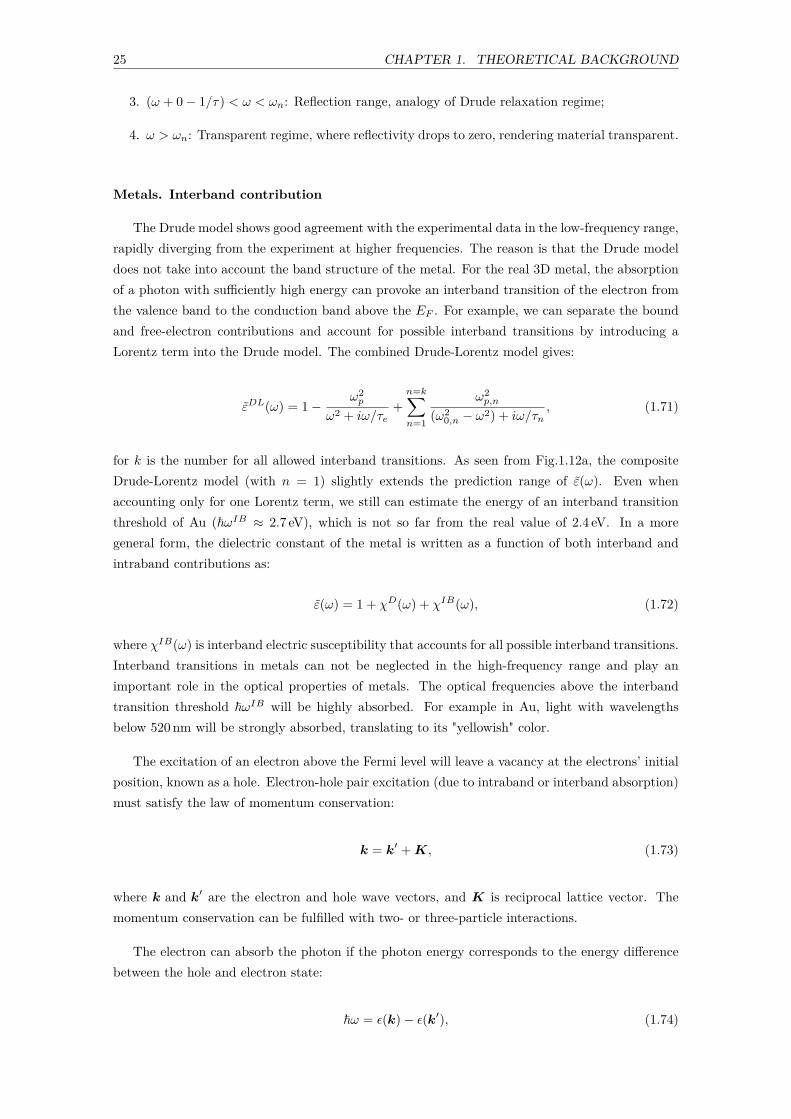
a) Coupling between photons and transverse optical phonon, called phonon-polariton. Redrawn from [32]and Wikipedia. b) High-frequency interband and low-frequency polariton contributions to ZnTe dielectricfunction. Both real and imaginary parts of the dielectric constant are flat in 8 − 400 THz range.High-frequency properties are redrawn from [33].
Figure 1.13 – Polariton dispersion curve and low-and-high frequency contributions to ZnTe dielectricconstant ε(ω).
where Di→j(ϵ, ℏω) is the energy-dependent density of states, which depends on the type of theoptical transition (d → s or p → s, for example). Then, the imaginary part of the dielectricfunction can be calculated using the Lindhard theory [31]:
ϵIB2 (ω) ∝ 1
ω2
∣∣M i→f∣∣2Ji→j(ℏω), (1.78)
where M i→f is the averaged electron momentum matrix element between the initial and finalbands. The 1/ω2 term comes from the electric dipole approximation. Interestingly, the Eq.1.78can be used to calculate the dielectric constant for the semiconductor [24], which does not includethe spin-orbit interaction. The real part of the dielectric function can be obtained by applying theKramers–Kronig relationship to Eq.1.78.
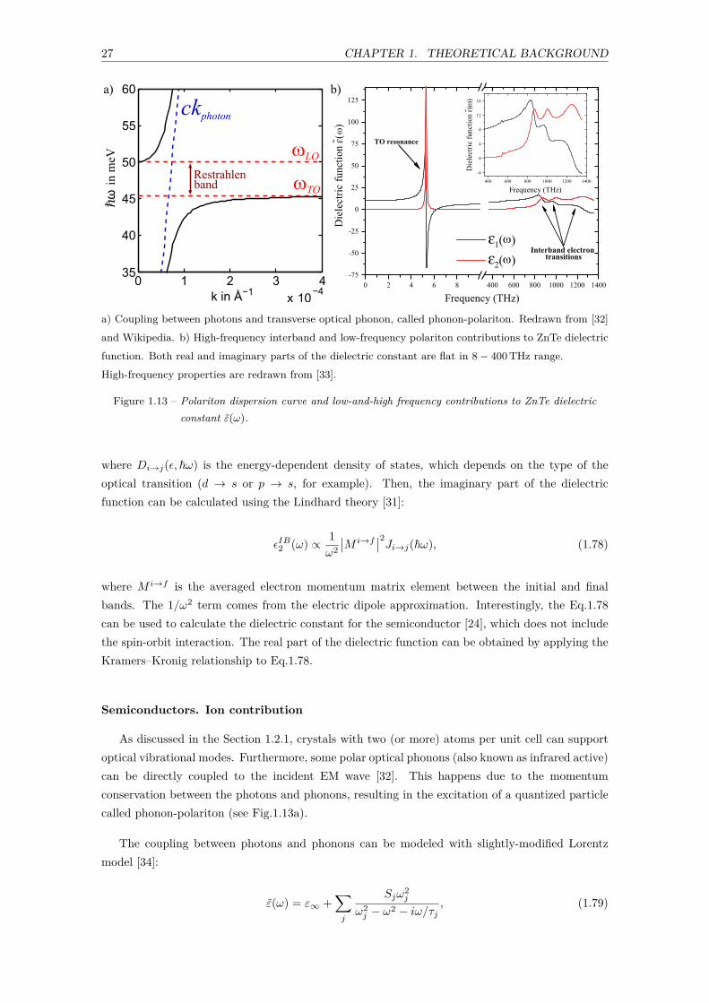
Semiconductors. Ion contribution
As discussed in the Section 1.2.1, crystals with two (or more) atoms per unit cell can supportoptical vibrational modes. Furthermore, some polar optical phonons (also known as infrared active)can be directly coupled to the incident EM wave [32]. This happens due to the momentumconservation between the photons and phonons, resulting in the excitation of a quantized particlecalled phonon-polariton (see Fig.1.13a).
The coupling between photons and phonons can be modeled with slightly-modified Lorentzmodel [34]:
ε(ω) = ε∞ +∑
j
Sjω2j
ω2j − ω2 − iω/τj
, (1.79)
28 CHAPTER 1. THEORETICAL BACKGROUND
where ε∞ is the dielectric constant of the ion background (i.e that of the conduction electrons,see the Eq.1.71). Here, we account for the contribution of all lattice oscillations that can interactwith EM fields, with eigenfrequency ωj , damping time τj , and dimensionless oscillator strengthSj . For most semiconductors, this equation can be simplified by restricting the sum to the firstlow-frequency TO mode:
ε(ω) = ε∞ + ST Oω2T O
ω2T O − ω2 − iω/τT O
. (1.80)
The oscillator strength ST O can be deduced from the DC dielectric constant [34] as:
ε(0) = εion + ST O. (1.81)
From the Lyddane-Sachs-Teller relation [35], Kurosawa [36] showed the direct connection betweenST O and the frequency difference between non-excited ωLO and resonant ωT O modes:
ST Oω2T O = ω2
LO − ω2T O. (1.82)
Due to the phonon-polariton coupling in ionic materials, this equation suggests that the latticewill strongly absorb photons with energies from ℏωT O to ℏωLO. This frequency range is called theReststrahlen band and ωT O sometimes referred to as Restrahl frequency.
To give a real example of phonon-polariton, the complex dielectric function of ZnTe from DCto 1400 THz is displayed in Fig.1.13b. The high-frequency contribution was redrawn from [33],showing well-pronounced interband contribution 2 to the dielectric constant around ≈ 800 THz(375 nm wavelength). Low-frequency phonon-polariton contribution calculated with parametersfrom [37], showing strong photon absorption around 5.3 THz. The presence of the Reststrahlenband is the main limiting factor for the semiconductor optics in the THz frequency range.
1.3.1.1 Nonlinear Regime
Light-matter interaction can modify the macroscopic polarization of the crystal (see Eq.1.63)proportional to its electric susceptibility. The total electronic displacement under the appliedelectric field is defined as:
D = ε0ε(ω)E(t) = ε0[1 + χ(ω)]E(t) = ε0E(t) + P (ω, t). (1.83)
For the electric fields with amplitudes comparable to the strength of the atomic field, i.e.:
Eat = e
4πε0a20
= 5.14 × 10¹¹,
[Vm
](1.84)
where a0 is the Bohr radius of the Hydrogen atom, can induce the nonresonant precession of themacroscopic polarization P [23]. This nonlinearity is accounted for by expressing the polarization
2. related to the excitation of excitons, which is not discussed here
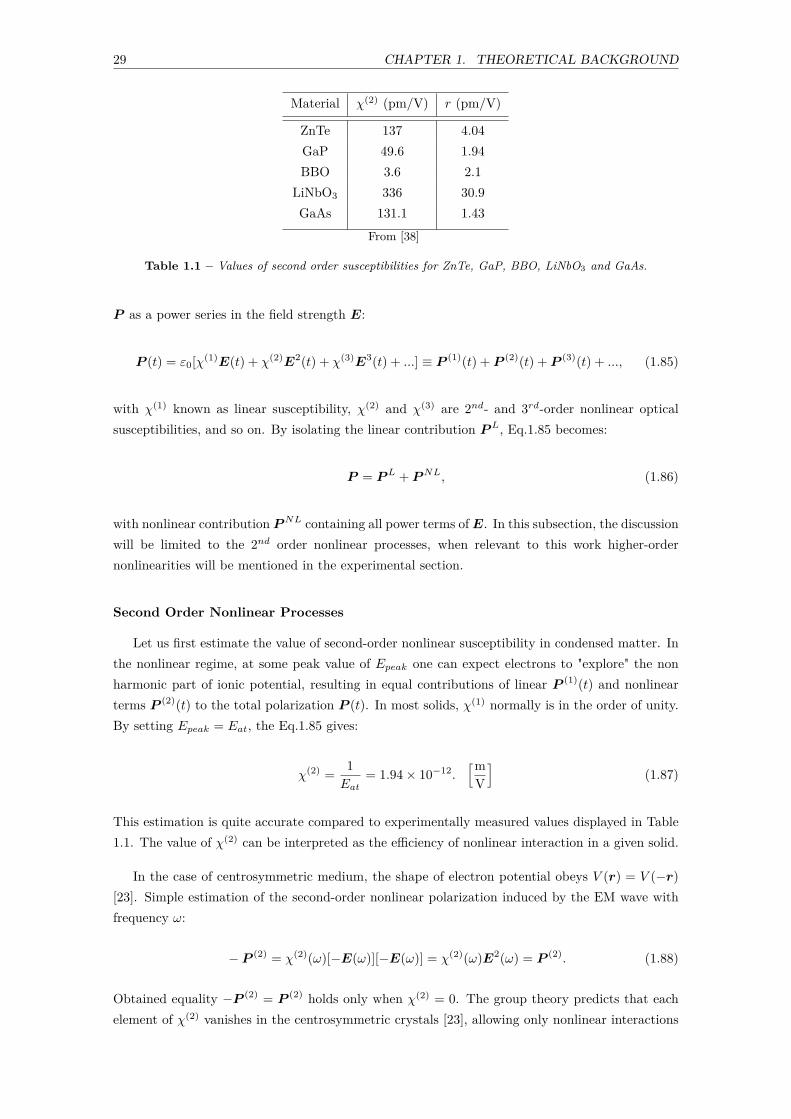
29 CHAPTER 1. THEORETICAL BACKGROUND
Material χ(2) (pm/V) r (pm/V)
ZnTe 137 4.04GaP 49.6 1.94BBO 3.6 2.1
LiNbO3 336 30.9GaAs 131.1 1.43
From [38]
Table 1.1 – Values of second order susceptibilities for ZnTe, GaP, BBO, LiNbO3 and GaAs.
P as a power series in the field strength E:
P (t) = ε0[χ(1)E(t) + χ(2)E2(t) + χ(3)E3(t) + ...] ≡ P (1)(t) + P (2)(t) + P (3)(t) + ..., (1.85)
with χ(1) known as linear susceptibility, χ(2) and χ(3) are 2nd- and 3rd-order nonlinear opticalsusceptibilities, and so on. By isolating the linear contribution P L, Eq.1.85 becomes:
P = P L + P NL, (1.86)
with nonlinear contribution P NL containing all power terms of E. In this subsection, the discussionwill be limited to the 2nd order nonlinear processes, when relevant to this work higher-ordernonlinearities will be mentioned in the experimental section.
Second Order Nonlinear Processes
Let us first estimate the value of second-order nonlinear susceptibility in condensed matter. Inthe nonlinear regime, at some peak value of Epeak one can expect electrons to "explore" the nonharmonic part of ionic potential, resulting in equal contributions of linear P (1)(t) and nonlinearterms P (2)(t) to the total polarization P (t). In most solids, χ(1) normally is in the order of unity.By setting Epeak = Eat, the Eq.1.85 gives:
χ(2) = 1Eat
= 1.94 × 10⁻¹².[m
V
](1.87)
This estimation is quite accurate compared to experimentally measured values displayed in Table1.1. The value of χ(2) can be interpreted as the efficiency of nonlinear interaction in a given solid.
In the case of centrosymmetric medium, the shape of electron potential obeys V (r) = V (−r)[23]. Simple estimation of the second-order nonlinear polarization induced by the EM wave withfrequency ω:
− P (2) = χ(2)(ω)[−E(ω)][−E(ω)] = χ(2)(ω)E2(ω) = P (2). (1.88)
Obtained equality −P (2) = P (2) holds only when χ(2) = 0. The group theory predicts that eachelement of χ(2) vanishes in the centrosymmetric crystals [23], allowing only nonlinear interactions

30 CHAPTER 1. THEORETICAL BACKGROUND
proportional to the odd powers of the electric field. However, nonlinear interactions of both oddand even power of E are allowed in noncentrosymmetric crystals, such as ZnTe, GaP, Beta BariumBorate (BBO), and more.
In the case of a noncentrosymmetric, isotropic medium with no dispersion, by taking intoaccount linear and nonlinear polarization, the driven Maxwell wave-equation becomes [23]:
∇2E − ε (1)
c2∂2E
∂t2= 1ε0c2
∂2P NL
∂t2, (1.89)
with ε (1) = 1 + χ(1), where the second order time derivative of nonlinear polarization acts as thesource term. We now examine the set of possible frequencies of electron polarization precession inthe nonlinear media. Let us apply two-color EM field:
E = E1e−iω1t + E2e
−iω2t + c.c., (1.90)
where E1 = A1eik1z and E2 = A1e
ik2z. With Euler’s formula cos(x) = (eix +e−ix)/2, the completesecond-order nonlinear polarization induced by the two-color EM field:
P (2)(t) = ε0χ(2)E(t)2 =
= 12ε0χ
(2)
E2
1 [cos(2ω1t) + cos((ω1 − ω1)t)]++E2
2 [cos(2ω2t) + cos((ω2 − ω2)t)]++2E1E2 cos[(ω1 + ω2)t] + 2E1E2 cos[(ω1 − ω2)t]
. (1.91)
With four different permutations between two frequencies ω1,2 the grouped contributions to thesecond order nonlinear polarization are:
P (2)(2ω1,2) = 12ε0χ
(2)E21,2 cos(2ω1,2t) Second harmonic generation (SHG);
P (2)(0ω) = 12ε0χ
(2)E21,2 Optical rectification (OR);
P (2)(ω1 + ω2) = ε0χ(2)E1E2 cos[(ω1 + ω2)t] Sum frequency generation (SFG);
P (2)(ω1 − ω2) = ε0χ(2)E1E2 cos[(ω1 − ω2)t] Difference frequency generation (DFG),
(1.92)
with SHG and OR being the special cases of SFG and DFG. The nonresonant movement of dipolemoments P NL will create the nonlinear current density JNL, equal to:
dP NL
dt= JNL. (1.93)
Such transient precession of the JNL can lead to the emission of light at different frequencies, asshown in Fig.1.14:
ENL(t) ∝ ∂JNL
∂t∝ ∂2P NL
∂t2. (1.94)
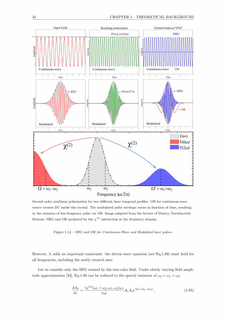
31 CHAPTER 1. THEORETICAL BACKGROUND
Second order nonlinear polarization for two different laser temporal profiles. OR for continuous-wavesource creates DC inside the crystal. The modulated pulse envelope varies in function of time, resultingin the emission of low-frequency pulse via OR. Image adapted from the lecture of Dmitry Turchinovich.Bottom: SHG and OR mediated by the χ(2) interaction in the frequency domain.
Figure 1.14 – SHG and OR for Continuous-Wave and Modulated laser pulses.
However, it adds an important constraint: the driven wave equation (see Eq.1.89) must hold forall frequencies, including the newly created ones.
Let us consider only the SFG created by the two-color field. Under slowly varying field ampli-tude approximation [23], Eq.1.89 can be reduced to the spatial variation of ω3 = ω1 + ω2:
dA3
dz= iχ(2)(ω1 + ω2, ω1, ω2)ω3
n3cA1A2e
i[k1+k2−k3]z, (1.95)
32 CHAPTER 1. THEORETICAL BACKGROUND
where n3 is crystal refractive index at ω3. This relation shows that the amplitude of the EM waveA3 at ω3 depends on the coupling between A1 and A2. We can introduce the so-called wavevector-,momentum- or phase mismatch as ∆k:
∆k = k1 + k2 − k3. (1.96)
By integration of Eq.1.95 over the distance d, the intensity of SFG radiation will be ∝ sinc2(∆kz/2).This means that the most efficient coupling between ω1 and ω2 is when k3 = k1 + k2. Usually, theincrease in light frequency ω is not compensated by the decrease in n, meaning that the perfectphase matching is rarely achieved. Multiple techniques were developed to minimize the ∆k, withbirefringent phase-matching being the most used one. In addition, wavevector mismatch is sensitiveto the crystal imperfections, laser beam quality, laser polarization state, and more. The discussionabout the phase-matching importance for the second-order nonlinear processes will continue in theexperimental section.
The remaining second-order nonlinear process of interest is the linear electro-optic effect, knownas the Pockels’ effect. Pockels’ effect explains the modification of refractive indices of the crystalwith an applied electric field. The contracted notation of the electrooptic effect is given by [23]:
∆(
1n2
)i
=∑
j
rijEj , (1.97)
where rij is the electrooptic tensor. Electrooptic effect can be pictured as follows: external DCelectric field will tilt the crystals’ optical axes by an amount ∝ ± 1
2n30rijEz, introducing the phase
retardation between two orthogonal light polarization components [23]:
Γ = (ni − nj)ωLc
= n30rijEjωL
c, (1.98)
with the speed of light in vacuum c, crystal thickness L and refractive index n0 in the absenceof electric field. Electrooptic effect is used for the high-frequency light modulation and detectionof the THz radiation, for example. Interestingly, the response time of a Pockels’ effect is in theorder of femtoseconds [39], allowing ultrafast switching of the light polarization with picosecondelectromagnetic pulses [40].
1.3.2 Polarization, reflection, and transmission of an electromagneticwave
Polarization
Light can be described as the periodic oscillation of the EM field in the xy plane travellingalong the z axis in Cartesian space. Mathematically, we can write equation of the complex EMfield as:
E = E0 exp [i(kz − ωt+ ϕ)], (1.99)
33 CHAPTER 1. THEORETICAL BACKGROUND
where E is the electric field with the field-wave vector k frequency ω and phase ϕ. At the giventime t, the direction of electric field can be expressed through the unit vectors x and y:
E = E0x exp [i(kz − ωt+ ϕx)]x + E0y exp [i(kz − ωt+ ϕy)]y. (1.100)
The direction of the electric field vector E along x and y axes is known as polarization of EMwave, and it is completely determined by the amplitudes and phase difference of the two orthogonalelectric field components. It can be written in the form of the two-element matrix, called Jonesvector:
E0 =[E0xe
iϕx
E0yeiϕy
]. (1.101)
With the Jones matrix notation, it is easy to represent the linearly, elliptically, and circularly po-larized light, including the polarization handedness direction. Randomly polarized or nonpolarizedlight does not require the use of the matrix notation. Linear polarization of the light in the xyplane, according to the Jones vector notation defined as:
E0 =[E0x
E0y
], (1.102)
with both E0x and E0y being real, non-zero field amplitudes. The periodically varying amplitudeof the electric field is inclined relative to the origin by the angle α = tan−1(E0y/E0x) [41]. E0x =1, E0y = 0 correspond to the linear light polarization along the x axis.
The general expression for the elliptically polarized light given as:
E0 =[
E0x
E0ye±iϕy
], (1.103)
where the sign of the ϕy defines the direction of the polarization rotation. If ϕy is positive,electric field direction will rotate in counterclockwise direction, when negative ϕy corresponds tothe clockwise handedness. The inclination angle of a polarization ellipse equals to the absolutevalue of ϕy. If E0x = E0y and ϕy = π/2, such EM wave has left-handed circular polarization.
Reflection and Transmission. Transfer matrix formalism
The transmission and reflection of an EM radiation at the singular plane surface depends onthe following set of variables: the angle of incidence θ1 and refraction θ2, the refractive indicesof incident n1 and refractive media n2, and the light polarization direction. The ratio betweenthe total, reflected and transmitted EM amplitudes can be derived from the Maxwell equationsat the boundary condition as shown elsewhere [41]. Obtained equations, namely, the polarization

34 CHAPTER 1. THEORETICAL BACKGROUND
Optical stack (two layers between the two half-spaces) with N=4. vi, wi are the amplitudes of theforward and backward propagating waves. Boundary conditions defined as vN−1 = t, wN−1 = 0 andv0 = 1, w0 = r. The image adapted from [42]
Figure 1.15 – Beam transmission and reflection from a multi layer film stack.
dependent Fresnel reflection r and transmission t coefficients read:
rs = n1 cos θ1 − n2 cos θ2
n1 cos θ1 + n2 cos θ2, rp = n2 cos θ1 − n1 cos θ2
n2 cos θ1 + n1 cos θ2
ts = 2n1 cos θ1
n1 cos θ1 + n2 cos θ2, tp = 2n1 cos θ1
n2 cos θ1 + n1 cos θ2
(1.104)
where subscripts p and s correspond to the parallel and perpendicular alignment of the electricfield polarization relative to the lights’ plane of incidence.
The transmission and reflection of light in a complex multilayer system can be approached fromthe view of the superposition of EM waves within the given layer. For example, the arbitrary Nlayer configuration has n = 0, 1, ..., N − 1 optically different interfaces, that contribute to the totaltransmission and reflection. An example of the N=4 stack system is shown in the Fig.1.15, definingthe amplitudes of the forward and backward propagating waves. The amplitudes of transmittedand reflected light arriving at the interface n = 1, 2, . . . , N − 2 can be expressed in the matrixnotation as: (
vn
wn
)= Mn
(vn+1
wn+1
), (1.105)
where the nth layer transfer matrix Mn is equal:
Mn ≡
[e−iδn 0
0 eiδn
][1 rn,n+1
rn,n+1 1
]1
tn,n+1, (1.106)
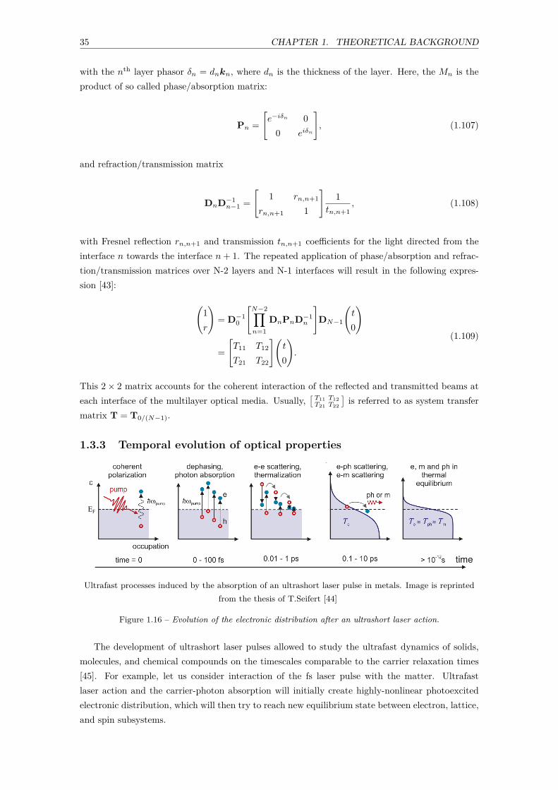
35 CHAPTER 1. THEORETICAL BACKGROUND
with the nth layer phasor δn = dnkn, where dn is the thickness of the layer. Here, the Mn is theproduct of so called phase/absorption matrix:
Pn =[e−iδn 0
0 eiδn
], (1.107)
and refraction/transmission matrix
DnD−1n−1 =
[1 rn,n+1
rn,n+1 1
]1
tn,n+1, (1.108)
with Fresnel reflection rn,n+1 and transmission tn,n+1 coefficients for the light directed from theinterface n towards the interface n+ 1. The repeated application of phase/absorption and refrac-tion/transmission matrices over N-2 layers and N-1 interfaces will result in the following expres-sion [43]:
(1r
)= D−1
0
[N−2∏n=1
DnPnD−1n
]DN−1
(t
0
)
=[T11 T12
T21 T22
](t
0
).
(1.109)
This 2 × 2 matrix accounts for the coherent interaction of the reflected and transmitted beams ateach interface of the multilayer optical media. Usually,
[T11 T12T21 T22
]is referred to as system transfer
matrix T = T0/(N−1).
1.3.3 Temporal evolution of optical properties
Ultrafast processes induced by the absorption of an ultrashort laser pulse in metals. Image is reprintedfrom the thesis of T.Seifert [44]
Figure 1.16 – Evolution of the electronic distribution after an ultrashort laser action.
The development of ultrashort laser pulses allowed to study the ultrafast dynamics of solids,molecules, and chemical compounds on the timescales comparable to the carrier relaxation times[45]. For example, let us consider interaction of the fs laser pulse with the matter. Ultrafastlaser action and the carrier-photon absorption will initially create highly-nonlinear photoexcitedelectronic distribution, which will then try to reach new equilibrium state between electron, lattice,and spin subsystems.

36 CHAPTER 1. THEORETICAL BACKGROUND
In metals, immediately after laser irradiation, the light-induced dipole polarization will createthe superposition of the electron states above and below EF . Simultaneously, light absorption willlead to an athermal, nonlinear distribution of the electron-hole pairs. The following energy trans-fer from the photoexcited carriers involves the multiple-particle interactions (electron-electron,electron-phonon, and electron-magnon), in order to bring the excited system to the thermal equi-librium.
The fastest many-particle relaxation process in the electron-electron interaction, which is hap-pening at the sup-picosecond time scale. Electron subsystem will thermalize via carrier multi-plication, reaching the Boltzmann distribution at elevated temperature [45]. Subsequently, thethermalization process between electronic, ionic, and spin baths occurs at the timescales of 0.1-10picoseconds. After electrons, magnons, and phonons have thermalized, heat dissipation to the en-vironment will occur, lasting more than 10 picoseconds. The sketch of the electron thermalizationprocess is displayed in the Fig.1.16.
Phenomenological Two and Three-Temperature Models
The phenomenological macroscopic model was established to explain the interaction betweenelectron, phonon, and spin subsystems of a solid at the ultrashort timescale with the evolution ofexperimental techniques. The first description of electron-phonon interaction after the absorptionof the laser pulse was proposed by the introduction of the energy balance equation [46]:
ce(Te)dTe
dt= −Ge−ph(Te − Tl) + I(t);
cL(Tl)dTl
dt= −Ge−ph(Tl − Te),
(1.110)
where Ge−ph is the electron-phonon coupling constant and I(t) is the laser source term. Thecarriers and phonon (heat) diffusion terms are neglected to simplify the model. I(t) applied onlyto the electron subsystem since the initial energy absorption is mediated only by the electrons.These equations were then denoted as the phenomenological two-temperature model (TTM) [47].
In the work of Beaurepaire et al. studying the ultrafast response of a ferromagnetic Ni, anextension of the TTM, which includes the electron-phonon-spin interaction was proposed [48].Beaurepaire’s system of equation, named as the three-temperature model (3TM), reads:
ce(Te)dTe
dt= −Ge−ph(Te − Tl) −Ge−m(Te − Ts) + I(t);
cs(Ts)dTs
dt= −Ge−m(Ts − Te) −Gm−ph(Ts − Tl);
cL(Tl)dTl
dt= −Ge−ph(Tl − Te) −Gm−ph(Tl − Ts),
(1.111)
with additional electron-magnon Ge−m and magnon-phonon Gm−ph coupling constants. Similarto the TTM, this model suggests that the heat exchange between electron, phonon, and spin sub-systems is proportional to the temperature difference between the two given baths. The respectivecoupling constant then defines the efficiency of the heat transfer (see Fig.1.17a). The coupling con-stants in simple metals Ge−m, Gm−ph and Ge−ph can be derived from the complex considerations
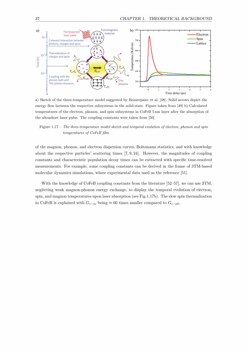
37 CHAPTER 1. THEORETICAL BACKGROUND
a) Sketch of the three-temperature model suggested by Beaurepaire et al. [48]. Solid arrows depict theenergy flow between the respective subsystems in the solid-state. Figure taken from [49] b) Calculatedtemperatures of the electron, phonon, and spin subsystems in CoFeB 5 nm layer after the absorption ofthe ultrashort laser pulse. The coupling constants were taken from [50]
Figure 1.17 – The three-temperature model sketch and temporal evolution of electron, phonon and spintemperatures of CoFeB film.
of the magnon, phonon, and electron dispersion curves, Boltzmann statistics, and with knowledgeabout the respective particles’ scattering times [7, 9, 24]. However, the magnitudes of couplingconstants and characteristic population decay times can be extracted with specific time-resolvedmeasurements. For example, some coupling constants can be derived in the frame of 3TM-basedmolecular dynamics simulations, where experimental data used as the reference [51].
With the knowledge of CoFeB coupling constants from the literature [52–57], we can use 3TM,neglecting weak magnon-phonon energy exchange, to display the temporal evolution of electron,spin, and magnon temperatures upon laser absorption (see Fig.1.17b). The slow spin thermalizationin CoFeB is explained with Ge−m being ≈ 60 times smaller compared to Ge−ph.

38 CHAPTER 1. THEORETICAL BACKGROUND
Chapter 2
Experimental Methods
Contents2.1 Introduction . . . . . . . . . . . . . . . . . . . . . . . . . . . . . . . . . 39
2.2 Pump-probe spectroscopy . . . . . . . . . . . . . . . . . . . . . . . . . 39
2.3 Terahertz generation and detection . . . . . . . . . . . . . . . . . . . 42
2.3.1 Terahertz generation: optical rectification . . . . . . . . . . . . . . . . . 432.3.2 Electrooptic terahertz detection . . . . . . . . . . . . . . . . . . . . . . . 45
2.4 THz time-domain spectroscopy . . . . . . . . . . . . . . . . . . . . . . 53
2.5 THz pulse shaping . . . . . . . . . . . . . . . . . . . . . . . . . . . . . . 56
2.1 Introduction
This chapter will focus on the description of the experimental techniques. First, we addressthe principle of the stroboscopic measurements, allowing us to record the transient dynamics ofthe material at the femtosecond and picosecond timescales. Second, we discuss the THz genera-tion via second-order nonlinear processes, and its particular configuration, the tilted-pulse frontmethod. The next part is devoted to the field-resolved detection of the pulsed THz radiation.After describing the electrooptic sampling technique, we calculate the detector response functionfor the crystals used in this work. In addition, we introduce and characterize the method of theelectrooptic detection improvement, which made possible the detection of the THz emission fromthe spintronic emitters discussed in the Chapter 4. The last subsection is about the basics ofthe THz Time domain spectroscopy (THz-TDS), where we present measured properties of silicon,silica, and x-cut Quartz in the THz range.
2.2 Pump-probe spectroscopy
Since its first implementation, the stroboscopic approach has dramatically improved and nowit is widely used in science, art, and the entertainment industry. For example, the fastest high-speed camera can record up to 1 Million frames per second (Phantom v2512) and is used in thefield of microfluidics and particle velocimetry [58]. In addition, the ultrafast photodiodes with therise-time of about 15 ps are now commercially available. However, since the temporal resolution
39

40 CHAPTER 2. EXPERIMENTAL METHODS
a) Sketch of the pump-probe experiment in transmission. The probe pulse is delayed in time with respectto the pump beam. We record the relative change in the probe’s transmission for the different temporaloverlaps between the pump and the probe. b) Example signal, obtained with the Bi2Te3 15 nm film, whileexcited with 800 nm pump and probed with 400 nm pulse. The sharp increase in the ∆T/T correspondsto the temporal overlap between the pump and the probe and consequent electron subsystem excitation.The subsequent exponential decay of the relative transmittance corresponds to electron-electron,electron-phonon coupling, and heat dissipation. In addition, one can reveal some coherent dynamics(high and low-frequency modulation of the ∆T/T ) with the pump-probe spectroscopy.
Figure 2.1 – Two-color pump-probe: Setup geometry and a typical recorded ∆T/T variation of 15 nmBi2Te3.
is limited by the shutter speed or carrier velocities in electronic detectors, it is impossible to usethese gating devices at the sub-picosecond timescales.
However, one can achieve sub-picosecond temporal resolution with pulsed laser radiation, wherethe width of the sampling pulse envelope can be as short as a couple of tens of attoseconds(10 × 10−18 s) [59–61]. In this thesis, ultrafast nonlinear spectroscopy was performed in pump-probe geometry. For this, the output laser beam is spatially split into two parts. The first part,called the pump, is used to excite the electronic subsystem of the sample, triggering the changeof the dielectric, structural or magnetic properties. The second part of the laser beam, is used tomonitor or probe the change in reflectance (∆R(τ)/R) or transmittance (∆T (τ)/T ) of the probebeam as the function of temporal delay τ between the pump and the probe pulses. The τ is adjustedby changing the optical path length of one of two beams (τ = ∆l/c), as shown in Fig.2.1a.
Today, various pump-probe based experimental techniques can measure the dynamics of asolid at the sub-picosecond timescales, using different parts of the EM spectrum of light. Forexample, experiments can be done with different configurations, such as all-optical pump-probe,time-resolved magneto-optical Kerr effect [48], time-resolved X-ray diffraction [62], and many more.All those pump-probe "derivatives" are designed to probe and/or excite a specific degree of freedomof matter. For example, during the all-optical pump-probe experiment, one measures the relativechange in the intensity of probing light with a central frequency of ωpr over the time τ , linkedto the temporal change in the dielectric function of the excited material. Let us write the total
41 CHAPTER 2. EXPERIMENTAL METHODS
electric field inside the studied media as [63]:
E(τ) = 12[Epr(kpr, τ) + Epump(kpump, τ) + E∗
pr(kpr, τ) + E∗pump(kpump, τ)
]. (2.1)
From the perturbation theory, the first order interaction describes the absorption of either the pumpand the probe beams, governed by χ(1) susceptibility. Next, the second order field-interactionincludes the second harmonic generation (SHG), optical rectification (OR) of pump and probebeam, and the frequency mixing between the pump and the probe (ωpr±ωpump) pulses, as discussedin the Section 1.3. In our case, we are only interested in the ωpr field components able to reachthe detector (i.e. propagating along the kpr). Here, the pump-probe interaction inside the media,that does not affect the change in kpr could be described in terms of third-order modification ofthe nonlinear polarization as [63]:
P (3)pump-pr(τ) =3ϵ0
2
∫dωpr
2πdωpump
2πdωpump
2π χ(3)(ωpr, ωpump,−ωpump)×
Epr(ωpr)Epump(ωpump)E∗pump(ωpump) exp[−i(ωpr + ωpump − ωpump)τ ],
(2.2)
where χ(3)(ωpr, ωpump,−ωpump) is the third order susceptibility, governing the particular interac-tion when the two pump pulses arrive simultaneously:
k = kpr + kpump − kpump = kpr, (2.3)
where kpr is conserved. In other words, for the short time-delays τ , the pump-probe experiment al-lows us to access the population relaxation of the irradiated matter. In the low-perturbation regime(for small ∆ε), we can express the time-dependent modification of the probe beam transmittanceor reflectivity as [24]:
∆TT
(ωpr, τ) = ∂ lnT∂ε1
(ωpr)∆ε1(ωpr, τ) + ∂ lnT∂ε2
(ωpr)∆ε2(ωpr, τ);
∆RR
(ωpr, τ) = ∂ lnR∂ε1
(ωpr)∆ε1(ωpr, τ) + ∂ lnR∂ε2
(ωpr)∆ε2(ωpr, τ),(2.4)
where ∆ε1(ωpr, τ) and ∆ε2(ωpr, τ) are time-dependent change of the real and imaginary partof complex dielectric function ε(ωpr), caused by the pump-pump population change within thematerial of interest.
In this work, we use a Ti:Al2O3 laser system based on the chirped-pulse amplification technique[64]. Our laser delivers 3 mJ pulses, centered around 800 nm wavelength, at 1 kHz repetition rate(3 W of mean power). The pulse duration was measured by a second-order intensity autocorrelatorand was found to be ≈ 165 fs (at FWHM).
The sketch of the experimental setup is shown in Fig.2.2. The beam is split with the ratio of90/10, where 90 % of power is used for the pump or THz pulse generation, and remaining 10 %of intensity is used as the probe. The 0.5 mm Beta Barium Borate (BBO) crystal, introduced inthe probe beam path, via SHG process converts the 800 nm into 400 nm light. The probe beam is

42 CHAPTER 2. EXPERIMENTAL METHODS
a) 800 nm pump and 400 nm probe setup. The Beta Barium Borate (BBO) crystal is used for thefrequency doubling of the probe beam. b)1 THz pump and 400 nm probe setup. The THz pulse isgenerated via the tilted-pulse front setup discussed in the manuscript. For both experimentalconfigurations, the pump beam is incident close to the normal incidence regarding the sample surface.For the probe, the angle of incidence is about 10 to 15°.
Figure 2.2 – Schema: The two pump-probe setups used in this work.
incident at ≈ 10° to 15° angle to the sample surface. The measurement of change in the probe beamtransmittance relies on the combination of balanced and lock-in synchronous detection techniques.For the balanced detection, 50 % of optical power is directed towards the reference photodiode.The signal part of the probe beam is focused onto the sample (with the spot size of ≈ 150 µm atFWHM) and is recorded by the signal photodiode of the NewFocus 2307 detector. The differencebetween the signal and reference inputs of NewFocus 2307 is fed to the SRS-830 Lock-in amplifier.The lock-in extracts the signal at the modulation frequency of the mechanical chopper (500 Hz)introduced in the pump beam path.
The conventional 800 nm pump/400 nm probe configuration is shown in the Fig.2.2a. Here, thepump is focused down to ≈ 200 µm spot diameter at normal incidence in respect to the samplesurface. Visible probe and near-IR pump beam sizes were measured with a CCD camera.
The main experimental configuration in this work is the THz pump/400 nm probe, shown in theFigure 2.2b. Here, THz pulse with a central frequency of 0.64 THz is generated with the tilted-pulsefront method, discussed later in the text. THz emitted from the lithium niobate crystal (LiNbO3)is collected and focused with a one-inch off-axis parabolic mirror (OAPM), having a two-inch focallength. The THz beam size was measured with a knife-edge method and was estimated to be equalto roughly 615 µm in diameter. The maximum THz pulse energy used in the experiment is around1.2 µJ. This gives us the maximum value of a peak electric field in the order of 275 kV cm−1.Details about the tilted pulse front method are discussed in the Section 2.3.1, and THz beam sizecharacterization is shown in the Appendix A.
2.3 Terahertz generation and detection
The part of the electromagnetic spectrum with corresponding photon energies in the range of0.1 eV-120 meV is called the THz range. Nowadays, terahertz pulses can be routinely generated

43 CHAPTER 2. EXPERIMENTAL METHODS
Material reff(pm/V) n800 nm0 n800 nm
gr nTHz αTHz(cm−1)CdTe (SC) 4.5 2.92 3.73 3.23 4.8GaAs (SC) 1.43 3.68 4.18 3.61 0.5GaP (SC) 0.97 3.18 3.57 3.34 1.9ZnTe (SC) 4.04 2.87 3.31 3.17 1.3GaSe (SC) 1.7 2.85 3.13 3.72 0.07LiTaO3 (FE) 30.5 2.145 2.22 6.42 46LiNbO3 (FE) 30.9 2.159 2.23 5.16 16DAST (OC) 77 2.38 3.31 2.4 150
Here, SC stands for semiconductor, FE is ferroelectric, and OC is an abbreviation of organic crystal.From [38]
Table 2.1 – Properties of the materials suitable for the optical rectification
in laboratory conditions via optical rectification in semiconductors [37, 65], ferroelectrics [66], or-ganic crystals [67], in air plasma [68], using synchrotron radiation [69], free-electron lasers [70],photoconductive switches [71] and spintronic emitters [1]. Furthermore, the THz radiation canbe detected and measured with multiple techniques, such as pyroelectric detection, electroopticsampling (EOS) [72], using photoconductive antennas [73,74], bolometers, air biased coherent de-tection [75], and THz radiation enhanced emission of fluorescence [76]. This section will discussthe THz generation via optical rectification and EOS detection principles.
Light propagating inside a nonlinear optical medium can create second-order nonlinear polar-ization P (2). As discussed in the Section 1.3.1.1, the rapidly varying femtosecond pulse envelopemay lead to transient precession of P (2) in the far- or mid-infrared frequency range due to thedifference-frequency mixing of a spectrally-broad light pulse. The second-order nonlinear suscepti-bility (χ(2)(Ω, ω1, ω2)) describes the efficiency of the optical rectification process. As an example,for F 43m space group (ZnTe, GaP, GaAs) the χ(2)(Ω, ω) tensor has only one non-vanishing diag-onal component and is linked to the nonlinear optic tensor dij(ωi, ωj) and electrooptic coefficientrij as [23,72]:
χ(2)ij (Ω, ωi, ωj) = 2dij = −
n2in
2jrij
4 . (2.5)
For simplicity, we will drop the tensor notation, and will speak in terms of the effective nonlin-ear susceptibilities χ(2)
eff (Ω, ω) and electrooptic coefficients reff(Ω). The list of some THz emitterssuitable for optical rectification is shown in the Table 2.1.
2.3.1 Terahertz generation: optical rectification
Since OR is a second-order nonlinear effect, the efficiency of the THz generation depends on theso-called velocity matching along the volume of the nonlinear crystal. For the in-phase precessionof P (2) inside the nonlinear crystal, the following condition needs to be satisfied [77]:
v800 nmgr = vTHz or n800 nm
gr = nTHz, (2.6)
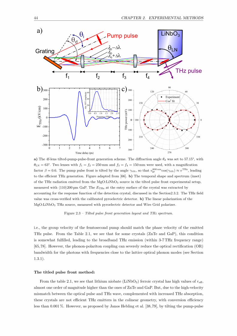
44 CHAPTER 2. EXPERIMENTAL METHODS
a) The 4f-lens tilted-pump-pulse-front generation scheme. The diffraction angle θd was set to 57.15°, withθLN = 63°. Two lenses with f1 = f2 = 250 mm and f3 = f4 = 150 mm were used, with a magnificationfactor β = 0.6. The pump pulse front is tilted by the angle γtilt, so that v800 nm
gr cos(γtilt) ≈ vTHz, leadingto the efficient THz generation. Figure adapted from [66]. b) The temporal shape and spectrum (inset)of the THz radiation emitted from the MgO:LiNbO3 source in the tilted pulse front experimental setup,measured with ⟨110⟩200 µm GaP. The ETHz at the entry surface of the crystal was extracted byaccounting for the response function of the detection crystal, discussed in the Section2.3.2. The THz fieldvalue was cross-verified with the calibrated pyroelectric detector. b) The linear polarization of theMgO:LiNbO3 THz source, measured with pyroelectric detector and Wire Grid polarizer.
Figure 2.3 – Tilted pulse front generation layout and THz spectrum.
i.e., the group velocity of the femtosecond pump should match the phase velocity of the emittedTHz pulse. From the Table 2.1, we see that for some crystals (ZnTe and GaP), this conditionis somewhat fulfilled, leading to the broadband THz emission (within 3-7 THz frequency range)[65,78]. However, the phonon-polariton coupling can severely reduce the optical rectification (OR)bandwidth for the photons with frequencies close to the lattice optical phonon modes (see Section1.3.1).
The titled pulse front method:
From the table 2.1, we see that lithium niobate (LiNbO3) ferroic crystal has high values of reff,almost one order of magnitude higher than the ones of ZnTe and GaP. But, due to the high-velocitymismatch between the optical pulse and THz wave, complemented with increased THz absorption,these crystals are not efficient THz emitters in the colinear geometry, with conversion efficiencyless than 0.001 %. However, as proposed by Janos Hebling et al. [38,79], by tilting the pump-pulse

45 CHAPTER 2. EXPERIMENTAL METHODS
front, one can overcome the velocity matching restrictions inside the LiNbO3 crystal. Using thistechnique, the group of K.Tanaka has achieved record generation efficiency of about 0.1 % withLiNbO3 crystals, reaching the peak THz field values of 1.2 MV cm−1 [66].
Fig.2.3a shows the geometry of the tilted-pulse front THz generation method. The diffractiongrating, in pair with the two lenses, is used to tilt the intensity front of the pump by an angle γtilt:
v800 nmgr cos(γtilt) ≈ vTHz. (2.7)
For the THz emission perpendicular to the crystal surface, the latter should be cut at the specificangle θLN, equal to the front-tilt angle γtilt. Then, the experimental parameters, such as diffractionangle θd, crystal angle θLN, and diffraction grating groove density p are chosen to satisfy the twofollowing relations [66]:
tan γtilt = mλ0p
n800 nmgr β1 cos θd
and tan θLN = n800 nmβ2 tan θd, (2.8)
with diffraction order m and pump pulse carrier wavelength λ0, where β1 and β2 are the horizontalmagnification factors of the 4-f system for the pump pulse front and the grating image, respectively.
In this work, we use MgO doped LiNbO3 cut at θLN = 63°. The 4-f imaging system is built withtwo spherical lenses with f1 = f2 = 250 mm and f3 = f4 = 150 mm, leading to the magnificationfactors of β1 = β2 = 0.6. The deviation angle of θ = θd − θi ≈ 17.3° was achieved with gratingperiod p = 1800 mm−1 and m = −1 diffraction order. The THz emitted from the LiNbO3 crystalwas collected with a one-inch off-axis parabolic mirror (OAPM) having a two-inch focal length.The THz temporal waveform, shown in Fig.2.3b, was recorded with a 200 µm ⟨110⟩ GaP crystal,in pair with two Wire Grid (WG) polarizers used as field attenuators. The estimation of peak THzpower was done with the EOS response function (see Section 2.3.2) and with the help of calibratedpyroelectric detector, accounting for the focused THz beam profile (see Appendix A). In addition,the THz power measured as a function of the WG polarizer angle confirms the linear polarizationof the LiNbO3 source (see Fig. 2.3c), which is perpendicular to the polarization of the pump pulse.
2.3.2 Electrooptic terahertz detection
Back in the 1980s, Auston [72] introduced a method of time-resolved gating of the THz electricfield with the stroboscopic approach, displayed in Fig.2.4a. Such EOS detection technique is basedon the Pockels effect (or linear Kerr-effect) in noncentrosymmetric crystals describing the electricfield induced birefringence. For the EOS detection, Pockels effect is used to measure the change inthe sampling pulse ellipticity inside the electrooptic crystal in the presence of the THz field.
Let us use the Jones Matrix formalism to describe the final polarization state of the samplingpulse, initially polarized along the x-axis [41]:
ppr =[
10
]. (2.9)
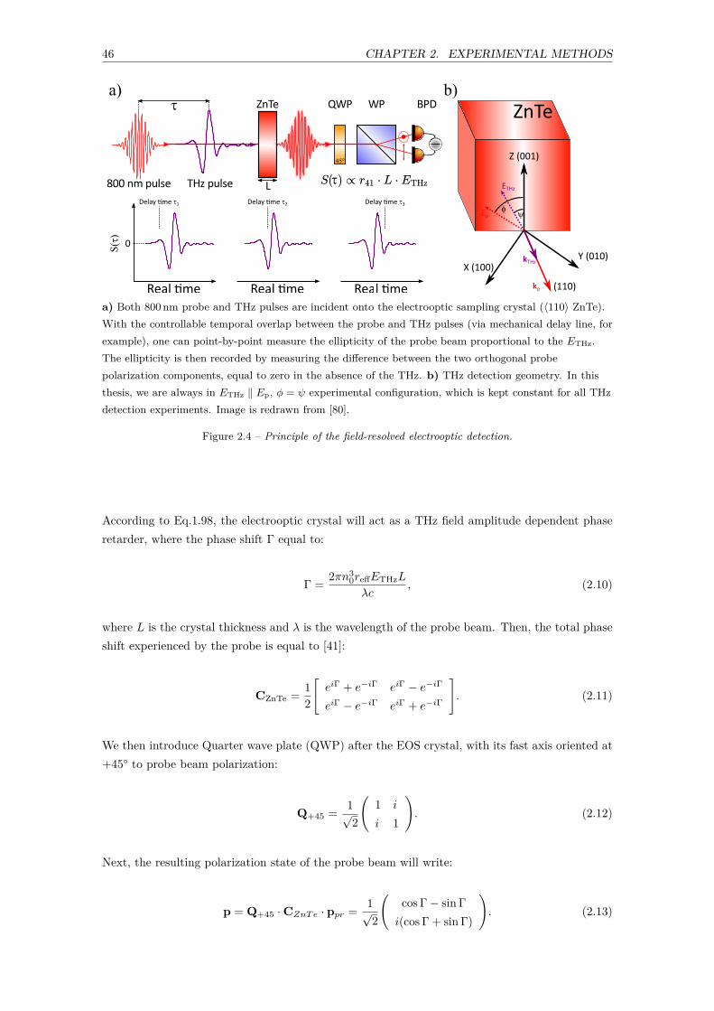
46 CHAPTER 2. EXPERIMENTAL METHODS
a) Both 800 nm probe and THz pulses are incident onto the electrooptic sampling crystal (⟨110⟩ ZnTe).With the controllable temporal overlap between the probe and THz pulses (via mechanical delay line, forexample), one can point-by-point measure the ellipticity of the probe beam proportional to the ETHz.The ellipticity is then recorded by measuring the difference between the two orthogonal probepolarization components, equal to zero in the absence of the THz. b) THz detection geometry. In thisthesis, we are always in ETHz ∥ Ep, ϕ = ψ experimental configuration, which is kept constant for all THzdetection experiments. Image is redrawn from [80].
Figure 2.4 – Principle of the field-resolved electrooptic detection.
According to Eq.1.98, the electrooptic crystal will act as a THz field amplitude dependent phaseretarder, where the phase shift Γ equal to:
Γ = 2πn30reffETHzL
λc, (2.10)
where L is the crystal thickness and λ is the wavelength of the probe beam. Then, the total phaseshift experienced by the probe is equal to [41]:
CZnTe = 12
[eiΓ + e−iΓ eiΓ − e−iΓ
eiΓ − e−iΓ eiΓ + e−iΓ
]. (2.11)
We then introduce Quarter wave plate (QWP) after the EOS crystal, with its fast axis oriented at+45° to probe beam polarization:
Q+45 = 1√2
(1 i
i 1
). (2.12)
Next, the resulting polarization state of the probe beam will write:
p = Q+45 · CZnT e · ppr = 1√2
(cos Γ − sin Γi(cos Γ + sin Γ)
). (2.13)

47 CHAPTER 2. EXPERIMENTAL METHODS
Finally, one can spatially separate two orthogonal probe polarization components (x and y)with a Wollaston prism (WP). Then, we can measure the difference between x and y intensitiesusing the balanced detection (See Fig.2.4a). In the absence of THz electric field inside the crystal,since |px|2 = |py|2, measured signal will be zero. Then, in the presence of ETHz (ETHz = 0), thenormalized power seen by the balanced photodiodes is:
S = |py|2 − |px|2
|px|2 + |py|2= sin(2Γ). (2.14)
For Γ ≪ 1, we can assume that sin(2Γ) ≈ 2Γ. Then, with Eq.2.10 and Eq.2.14 we can write:
Γ = 2πn30reffETHzL
λ⇒ ET Hz = Sλ
πn30reffL
(2.15)
By changing the temporal overlap between the short sampling pulse and the THz waveform, onecan point-by-point record S(τ) (see Eq.2.14), and thus measure the shape of the THz electric field.
Moreover, the efficiency of the THz detection strongly depends on the orientation of the THzpolarization (angle ψ) and the probe beam polarization with respect to the crystal z-axis (angleϕ), depicted in the Fig.2.4b. Planken et al. [80] have deduced the dependence of the electroopticsignal strength on the angles ψ and ϕ:
S(τ) ∝ (cosψ sin 2ϕ+ 2 sinψ cos 2ϕ). (2.16)
We remind that ψ and ϕ are the azimutal angles between the ETHz and Ep in respect to electroopticdetection crystal z-axis. In this thesis, we have set ϕ = ψ (meaning that Ep ∥ ETHz), and we rotatedthe crystal to obtain maximum possible signal.
THz detection sensitivity improvement: In Chapter 4, we sample low-amplitude ETHz(τ)fields, which requires a lot of averaging in the conventional electrooptic detection scheme (withQ+45). To improve the sensitivity of the EOS, we use the simple experimental technique firstdescribed by J. A. Johnson et al. [81] and then further simplified by P. Krauspe et al. [82], with atheory established by J. Brunner et. al. [83].
Experimentally, this approach could be regarded as the decrease in the ratio between the opticalbias and the effective electrooptic signal. In a general way, the measured EOS signal (see Eq.2.14)can be defined as the function of Γ and Quarter Wave Plate (QWP) angle α (see Fig.2.5a) as [82]:
arcsin(S(α,Γ)) = 2Γsin(2α) + 2cot(2α)2 · Γ2, (2.17)
where the first term is the linear part of the signal, directly proportional to ETHz. The secondterm is the quadratic contribution, proportional to |ETHz|2. One can retrieve the conventionalEOS equation (Eq.2.14) for α = ±45°, since the quadratic term and the α-dependence can be
48 CHAPTER 2. EXPERIMENTAL METHODS
neglected. However, for small ETHz-induced phase (Γ ≪ 1, sin(Γ) ≈ Γ), the subtraction of signalsmeasured for ±α yields:
S(α,Γ) − S(−α,Γ) = 4Γsin(2α) , (2.18)
returning only the linear contribution to the S(τ), but improved (or enhanced) by the factor of1/ sin 2α. In analogy, the addition of the two signals recorded for ±α:
S(α,Γ) + S(−α,Γ) = 4 cot(2α)2 · Γ2 (2.19)
will contain only information about the quadratic contribution to the measured EOS signal.
To check this method, we first use the 500 µm ZnTe emitter and detector, and measure THzwaveform in the function of the QWP angle α. For α = 45°, a variable attenuator (VA, shownin Fig.2.5a) needs to be used to re-balance the photodiodes. Fig.2.5b depicts the change in S(τ)with the decrease of QWP angle α. The data for α > 1.7° is not shown, since the waveform isindistinguishable from the one recorded for α ≈ 45°. For α < 1.7°, the nonlinear contributionstarts to dominate, resulting in the noticeable distortion of the measured THz field [81].
Since we can not control QWP angle α with high precision, manual rotation of the mechanicalcomponents can lead to questionable eperimental reproducibility of the undistorted THz waveformretrieval, especially for small values of α. Due to this mechanical limitation, the study of the THzemission from spintronic emitters was done for the fixed value of α. QWP angle α was selected sothat the quadratic contribution to S(τ) is negligible (i.e. 2Γ/sin(2α) ≪ 2cot(2α)2 ·Γ2, see Eq.2.17).In this case, the measurement for ±α can be avoided.
In order to select the appropriate value of α, we replaced the 500 µm ZnTe crystal with spintronicTHz emitter CoFeB(20 nm)/MgO(6 nm) 1. All other experimental parameters were kept the sameas before. The recorded THz waveforms for α ≈ 0.25° and α ≈ 45° are shown in the Fig.2.5c.When two measurements normalized by the peak-to-peak amplitude of the respective signal, perfectoverlap of the normalized THz waveforms indicates the absence of nonlinear distortion (see insetof Fig.2.5c). This is expected, since THz emitted from CoFeB(20)/MgO(6) is way weaker thanthe one generated with 500 µm ZnTe crystal, roughly by the factor of 800. In addition, the field-induced phase retardation Γ of CoFeB(20 nm)/MgO(6 nm) at α = 0.25° is still smaller than thesignal obtained 0.5 mm ZnTe at α ≈ 45°.
From this, in the absence of the signal distortion, one can directly estimate the detectivityenhancement factor ΛEOS as:
ΛEOS = S(α,Γ)S(45°,Γ) , (2.20)
1. Discussed more in the Chapter 4
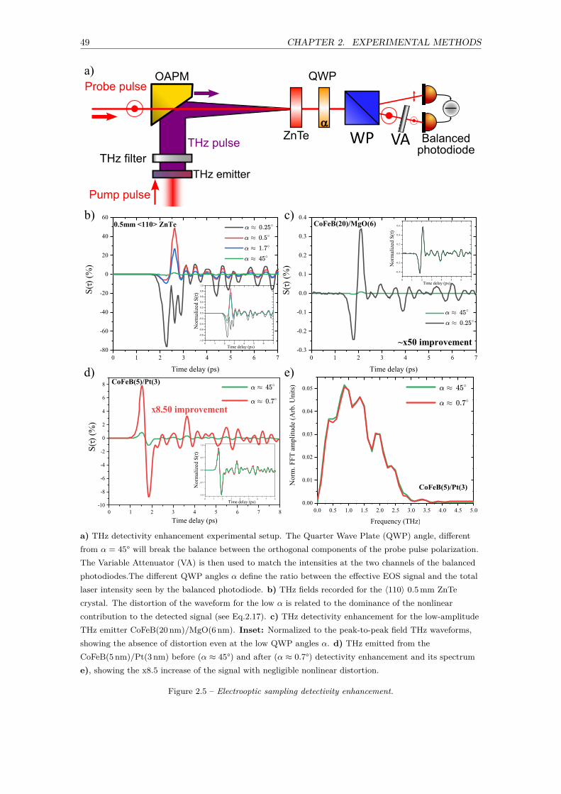
49 CHAPTER 2. EXPERIMENTAL METHODS
a) THz detectivity enhancement experimental setup. The Quarter Wave Plate (QWP) angle, differentfrom α = 45° will break the balance between the orthogonal components of the probe pulse polarization.The Variable Attenuator (VA) is then used to match the intensities at the two channels of the balancedphotodiodes.The different QWP angles α define the ratio between the effective EOS signal and the totallaser intensity seen by the balanced photodiode. b) THz fields recorded for the ⟨110⟩ 0.5 mm ZnTecrystal. The distortion of the waveform for the low α is related to the dominance of the nonlinearcontribution to the detected signal (see Eq.2.17). c) THz detectivity enhancement for the low-amplitudeTHz emitter CoFeB(20 nm)/MgO(6 nm). Inset: Normalized to the peak-to-peak field THz waveforms,showing the absence of distortion even at the low QWP angles α. d) THz emitted from theCoFeB(5 nm)/Pt(3 nm) before (α ≈ 45°) and after (α ≈ 0.7°) detectivity enhancement and its spectrume), showing the x8.5 increase of the signal with negligible nonlinear distortion.
Figure 2.5 – Electrooptic sampling detectivity enhancement.
50 CHAPTER 2. EXPERIMENTAL METHODS
which, for CoFeB(20 nm)/MgO(6 nm) is equal to:
ΛEOS = S(0.25°,Γ)S(45°,Γ) ≈ 50. (2.21)
All the THz signals discussed in the Chapter 4, were measured with this technique. However,at first all signals were recorded without the EOS detectivity enhancement. Then, the experimentwas repeated for the fixed value of α ≈ 0.7°, for which THz detected from all spintronic emittersshowed no distortion. Figure 2.18d displays the "raw" (α = 45°) and enhanced signal (α ≈ 0.7°)of the most efficient spintronic emitter in our disposal, CoFeB(5)/Pt(3). For the enhancementfactor ΛEOS of about 8.5, both the THz waveform and its spectrum remains unchanged, indicatingthe presence of only linear contribution to S(τ). In addition, the dependence of emitted ETHz
amplitude on the NIR pump power was measured at conventional α ≈ 45°, in order to be free fromthe possible detection nonlinearities present for the higher-amplitude THz fields.
In theory, for the low electric field amplitudes, the improvement factor ΛEOS can be increasedeven further, but mainly limited by the damage threshold of the EOS crystal and the reasonableamount of optical power required for the balanced detection. For example, one can increasethe sampling beam size in order to reduce the optical fluence Φ inside the detection crystal. Inaddition, one can replace a conventional balanced detector by the pair of avalanche photodiodesfor low α < 0.1°. Ultimately, this technique can be applied for any polarization-sensitive detection.In principle, this THz detectivity enhancement technique based on the QWP-detuning can be usedfor both kHz and MHz oscillators, but it requires an excessive sampling pulse optical power density,and signal-to-noise ratio may be limited by the electronic noise in the case of MHz oscillators.
Electrooptic response function: Since EOS is governed by the crystals’ effective electroopticcoefficient reff, the detection efficiency and bandwidth strongly depend on the ionic and the opticalproperties of the detector. For example, when THz phase - sampling pulse group velocity mismatchis negligible, and with THz pulse having frequency components out of the range of detection crystallattice optical phonon resonances, measured signal will be the direct replica of the THz electricfield, i.e., S(τ) ∝ ETHz. In reality, however, detected signal S(τ) is a result of the convolutionbetween the frequency-dependent detector response and THz electric field [37,65,78]:
S(τ) = ETHz(τ) ⊛ hEOS(τ), (2.22)
where hEOS(τ) is the EOS response function of the nonlinear medium, and ⊛ is the convolutionoperator. In the frequency domain, the latter equation can be rewritten as:
S(Ω) = ETHz(Ω) × hEOS(ω,Ω), (2.23)
where ω and Ω are the angular frequencies of the Near-IR sampling pulse and THz waveform,respectively.
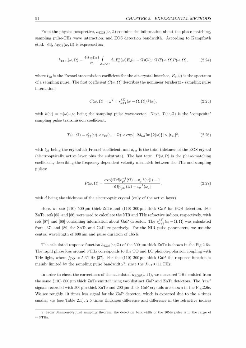
51 CHAPTER 2. EXPERIMENTAL METHODS
From the physics perspective, hEOS(ω,Ω) contains the information about the phase-matching,sampling pulse-THz wave interaction, and EOS detection bandwidth. According to Kampfrathet.al. [84], hEOS(ω,Ω) is expressed as:
hEOS(ω,Ω) = 4it12(Ω)c2
∫ω>Ω
dωE∗s (ω)Es(ω − Ω)C(ω,Ω)T (ω,Ω)P (ω,Ω), (2.24)
where t12 is the Fresnel transmission coefficient for the air-crystal interface, Es(ω) is the spectrumof a sampling pulse. The first coefficient C(ω,Ω) describes the nonlinear terahertz - sampling pulseinteraction:
C(ω,Ω) = ω2 × χ(2)eff (ω − Ω,Ω)/k(ω), (2.25)
with k(ω) = n(ω)ω/c being the sampling pulse wave-vector. Next, T (ω,Ω) is the "composite"sampling pulse transmission coefficient:
T (ω,Ω) = t∗12(ω) × t12(ω − Ω) × exp[−2dtotImk(ω)] × |t21|2, (2.26)
with t21 being the crystal-air Fresnel coefficient, and dtot is the total thickness of the EOS crystal(electrooptically active layer plus the substrate). The last term, P (ω,Ω) is the phase-matchingcoefficient, describing the frequency-dependent velocity mismatch between the THz and samplingpulses:
P (ω,Ω) =exp(iΩd[v−1
ph (Ω) − v−1g (ω)]) − 1
iΩ[v−1ph (Ω) − v−1
g (ω)], (2.27)
with d being the thickness of the electrooptic crystal (only of the active layer).
Here, we use ⟨110⟩ 500 µm thick ZnTe and ⟨110⟩ 200 µm thick GaP for EOS detection. ForZnTe, refs [85] and [86] were used to calculate the NIR and THz refractive indices, respectively, withrefs [87] and [88] containing information about GaP detector. The χ(2)
eff (ω − Ω,Ω) was calculatedfrom [37] and [89] for ZnTe and GaP, respectively. For the NIR pulse parameters, we use thecentral wavelength of 800 nm and pulse duration of 165 fs.
The calculated response function hEOS(ω,Ω) of the 500 µm thick ZnTe is shown in the Fig.2.6a.The rapid phase loss around 3 THz corresponds to the TO and LO phonon-polariton coupling withTHz light, where fT O ≈ 5.3 THz [37]. For the ⟨110⟩ 200 µm thick GaP the response function ismainly limited by the sampling pulse bandwidth 2, since the fT O ≈ 11 THz.
In order to check the correctness of the calculated hEOS(ω,Ω), we measured THz emitted fromthe same ⟨110⟩ 500 µm thick ZnTe emitter using two distinct GaP and ZnTe detectors. The "raw"signals recorded with 500 µm thick ZnTe and 200 µm thick GaP crystals are shown in the Fig.2.6c.We see roughly 10 times less signal for the GaP detector, which is expected due to the 4 timessmaller reff (see Table 2.1), 2.5 times thickness difference and difference in the refractive indices
2. From Shannon-Nyquist sampling theorem, the detection bandwidth of the 165 fs pulse is in the range of≈ 3 THz.
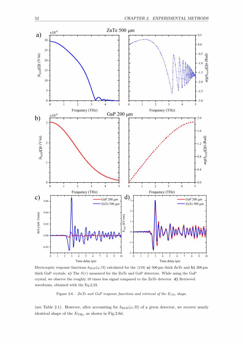
52 CHAPTER 2. EXPERIMENTAL METHODS
Electrooptic response functions hEOS(ω,Ω) calculated for the ⟨110⟩ a) 500 µm thick ZnTe and b) 200 µmthick GaP crystals. c) The S(τ) measured for the ZnTe and GaP detectors. While using the GaPcrystal, we observe the roughly 10 times less signal compared to the ZnTe detector. d) Retrievedwaveforms, obtained with the Eq.2.23.
Figure 2.6 – ZnTe and GaP response functions and retrieval of the ETHz shape.
(see Table 2.1). However, after accounting for hEOS(ω,Ω) of a given detector, we recover nearlyidentical shape of the ETHz, as shown in Fig.2.6d.
53 CHAPTER 2. EXPERIMENTAL METHODS
One should note that Fig.2.6d gives us the approximate shape of ETHz(τ) in front of thedetection crystal. In Chapter 3, we apply such hEOS(ω,Ω)-deconvolution to the THz emittedfrom LiNbO3 crystal, since the information about the ETHz waveform just in front of the sampleis essential for the measurements interpretation and first-principle calculations. However, dueto the fact that the THz emission experiments presented in Chapter 4 were done for the samedetection crystal, it allows us to directly compare all the measured signals. In addition, one canestimate the electric field waveform at the emitter position, taking into account the spatio-temporaltransformation focusing distortions of the THz pulse [90,91].
2.4 THz time-domain spectroscopy
The THz time-domain spectroscopy (THz-TDS) allows studying the static or transient materialproperties in the far-IR/THz range. The review of the different sources used for the THz-TDS,potential noise sources, the influence of the experimental settings were described by J. Neu and C.A. Schmuttenmaer [92].
Free-standing film or bare substrate: The dielectric function of the free-standing filmcan be measured as follows. First, the waveform of the reference pulse Sref(τ) with no sample inthe path of THz, in pair with the noise Snoise(τ) 3, propagating through the free space is recorded.Second, the sample with the thickness d is introduced in the THz beam path, and sample signalSsam(τ) is recorded. Next, one can write the ratio between the reference and sample signals in thefrequency domain as:
H(Ω) = S(Ω)sam
S(Ω)ref= Esam(Ω) × hEOS(ω,Ω)
Eref(Ω) × hEOS(ω,Ω) = Esam(Ω)Eref(Ω) , (2.28)
where the response function of the detector is mathematically irrelevant. In this type of experiment,the signal-to-noise ratio is really important, especially for frequencies close to the detector latticeresonance modes, for example.
Next, the amplitude A(Ω) and the phase ϕ(Ω) of the THz-TDS ratio H(Ω) are calculated. Byknowing the thickness of the sample d, the refractive index of the free-standing film n(Ω) is givenas [93]:
n(Ω) = 1 + c
Ωdϕ(Ω). (2.29)
From the calculated refractive index, the absorption coefficient α(Ω) can be estimated as:
α(Ω) = −2d
lnA(Ω) [n(Ω) + 1]2
4n(Ω)
= 2ωIm(k(Ω))
c. (2.30)
However, it is important to know the sensitivity of the experiment. The ratio between Sref(Ω)/Snoise(Ω)
3. When the THz source is blocked.

54 CHAPTER 2. EXPERIMENTAL METHODS
Refractive index n and absorbance α of a) High-resistivity float-zone Si wafer, b) High-DensityPolyethylene (HDPE) and c) Float-Zone Glass substrate. Shaded regions represent the unreliablefrequency range, i.e. where neither n nor α could be estimated with the THz-TDS experiment. Thevalues were calculated with Eq.2.29 and Eq.2.30. Dashed blue line corresponds to the THz-TDSresolution limit, defined by the response function of ZnTe.
Figure 2.7 – THz refractive indices and absorbance of the free standing Si, HDPE and Glass substrates.
is used to estimate the experimental dynamical reserve (DR) 4 of the experiment [93]:
αmax(Ω) = 2 lnDR(Ω) 4n(Ω)
([n(Ω) + 1]2
. (2.31)
4. Or signal-to-noise ratio.
55 CHAPTER 2. EXPERIMENTAL METHODS
It should be noted, that α(Ω) < αmax(Ω) is the criterion of the reliable measurement of both n andα. In addition, we manually limit the THz-TDS resolution up to 3 THz, close to the high-distortionof the hEOS (see Fig.2.6a).
Next, we have measured refractive indices and absorption coefficients of the High-ResistivityFloat-Zone Silicon (HRFZS) wafer, High-Density Polyethylene (HDPE), and Float-Zone Glasssubstrates (see Fig.2.7). We observe a flat refractive index and absence of absorption in HRFZSand HDPE, in good agreement with the literature [94, 95]. On the other hand, the glass showsstrong n(Ω) and α(Ω) frequency dependence, which leads to the strong distortion of the transmittedTHz pulse [96].
The primary purpose of the HDPE sheet (with band-gap energy in the range of 4.6 eV or270 nm [97]) is to diffuse and filter out the pump beam, used for the THz generation in the collinearconfiguration (ZnTe, GaP, spintronic emitters). In addition, we use HRFZS wafer to completelyremove any remaining pump residue. The HRFZS THz transmission, placed after the single HDPEsheet, was estimated to THRFZS = 67 %, in good agreement with multiple reports [66, 94, 98].However, the removal of HDPE sheet before the HRFZS leads to the photoexcitation and pump-power dependent THz absorption of the latter, as discussed in the Appendix F.
Thin metallic films: For the thin film with the thickness dfilm deposited onto the thicksubstrate, the THz amplitude transmission H(Ω) (see Eq.2.28) will be the product of the THzpulse multiple reflections at the film interfaces, paired with THz absorption in the metal film andthe substrate [99]:
H(Ω) = t12t23t31 · exp[ik2(Ω)dfilm] · exp[ik3(Ω)dsub]1 + r12r23 exp[2ik2(Ω)dfilm] , (2.32)
where k1, k2 and k3 are the complex THz wave vectors in air, metallic film and substrate, respec-tively. However, one can simplify the latter equation,if the THz-TDS signal of the bare substrateSsub(Ω) was used as the reference [100]:
H(Ω) = Ssam(Ω)Ssub(Ω) · exp[i(n3(Ω) − 1)∆dsubΩ/c], (2.33)
where we account for the reference and sample substrate thickness mismatch with ∆dsub. If themetallic film is smaller than the THz wavelength and penetration depth, the Eq.2.32 becomes:
H(Ω) = n2(Ω) + n3(Ω)n2(Ω) + n3(Ω) + Z0
∫ dfilm0 dzσ(Ω)
, (2.34)
with the free space impedance Z0 = 377 Ω. Here, the frequency dependent conductivity σ(Ω) canbe calculated with the Drude model:
σ(Ω) = σDC
1 − iΩ/τe, (2.35)
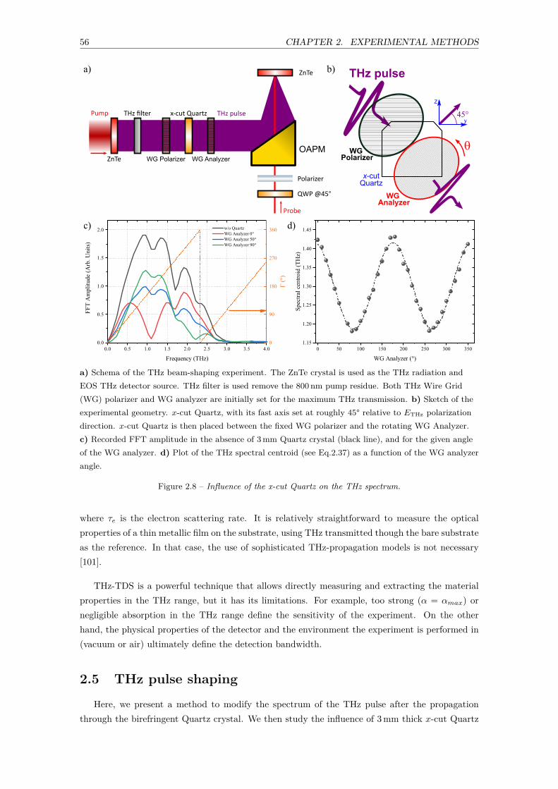
56 CHAPTER 2. EXPERIMENTAL METHODS
a) Schema of the THz beam-shaping experiment. The ZnTe crystal is used as the THz radiation andEOS THz detector source. THz filter is used remove the 800 nm pump residue. Both THz Wire Grid(WG) polarizer and WG analyzer are initially set for the maximum THz transmission. b) Sketch of theexperimental geometry. x-cut Quartz, with its fast axis set at roughly 45° relative to ETHz polarizationdirection. x-cut Quartz is then placed between the fixed WG polarizer and the rotating WG Analyzer.c) Recorded FFT amplitude in the absence of 3 mm Quartz crystal (black line), and for the given angleof the WG analyzer. d) Plot of the THz spectral centroid (see Eq.2.37) as a function of the WG analyzerangle.
Figure 2.8 – Influence of the x-cut Quartz on the THz spectrum.
where τe is the electron scattering rate. It is relatively straightforward to measure the opticalproperties of a thin metallic film on the substrate, using THz transmitted though the bare substrateas the reference. In that case, the use of sophisticated THz-propagation models is not necessary[101].
THz-TDS is a powerful technique that allows directly measuring and extracting the materialproperties in the THz range, but it has its limitations. For example, too strong (α = αmax) ornegligible absorption in the THz range define the sensitivity of the experiment. On the otherhand, the physical properties of the detector and the environment the experiment is performed in(vacuum or air) ultimately define the detection bandwidth.
2.5 THz pulse shaping
Here, we present a method to modify the spectrum of the THz pulse after the propagationthrough the birefringent Quartz crystal. We then study the influence of 3 mm thick x-cut Quartz
57 CHAPTER 2. EXPERIMENTAL METHODS
crystal on the THz pulse polarization and spectrum. In this experiment, we use a 500 µm ZnTecrystal as both THz source and detector.
First, we have recorded the reference THz spectrum in the absence of the x-cut Quartz, dis-played as a black curve in Fig.2.8c. Next, we placed the x-cut Quartz crystal between the Wire GridWG polarizer analyzer, with its fast axis oriented at θQuartz ≈ 45° relative to ETHz polarization,and measured the THz spectrum in the function of the WG analyzer angle (see Fig.2.8b).
The rotation of the WG analyzer will select a specific polarization component of the ETHz,which is then directed towards the EOS detector. To be in an optimal EOS detection condition,we have kept the angles between z-axis of the detection crystal, ETHz and Ep field vectors fixedthrough the experiment (as described in the Section 2.3.2).
THz spectra, measured for θ = 0°, 50°, and 90° are shown in the Fig.2.8c. The observedmodification of the THz spectrum amplitude, can be explained with the Eq.1.98. For this wecan calculate the frequency-dependent phase shift within 0 to 4 THz range, experienced by thesampling pulse:
Γ(Ω) = (ne − no)ΩLc, (2.36)
with x-cut Quartz thickness L = 3 mm. We took no = 2.113 and ne = 2.156 values from themanufacturer, measured at 1 THz 5, and do not account for the possible frequency dependentne−o(Ω). The result of the calculation is shown in the Fig.2.8c as orange dash-dot line. Forexample, we see that the x-cut Quartz should be analogous to the half-waveplate at frequency of1 THz, or act as quarter-plate at 0.5 THz. This is why we observe close to zero FFT amplitude at1 THz for WG analyzer fixed at θ = 0° (behaves as λ/2 plate), and no change at 0.5 THz frequency(behaves as λ/4 plate).
We then can calculate the spectral centroid in the function of the WG analyzer angle, i.e. tosee how spectrum center of mass evolves for selected ETHz projection:
Spectral Centroid =∑N−1
n=0 nA[n]∑N−1n=0 A[n]
, (2.37)
where A[n] is the FFT amplitude corresponding to the n-th point of the spectrum. Figure 2.8dshows the Spectral Centroid as a function of the WG analyzer angle θ. As a result, due to thestrong Γ(Ω) frequency dependence in Quartz, the THz spectral centroid of the ZnTe crystal canbe tuned in 1.2-1.4 THz frequency range.
One should note that the most direct way to shape the spectrum of the THz pulse is to changethe thickness of the electrooptic crystal (see Eq.2.27). As an alternative, the tilted pulse front setup(TPFS) can be realigned to satisfy the phase-matching condition within 0.5-3 THz range [38,102].However, due to the high realignment complexity of the TPFS setup, the 3 mm x-cut Quartzcrystal could be a simple alternative for the post-emission THz pulse-shaping.
5. See THz materials section on the Tydex website.
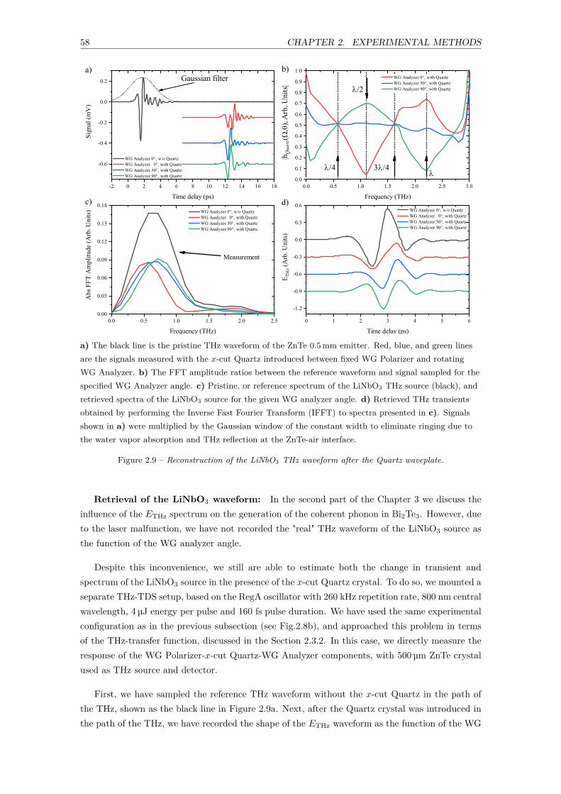
58 CHAPTER 2. EXPERIMENTAL METHODS
a) The black line is the pristine THz waveform of the ZnTe 0.5 mm emitter. Red, blue, and green linesare the signals measured with the x-cut Quartz introduced between fixed WG Polarizer and rotatingWG Analyzer. b) The FFT amplitude ratios between the reference waveform and signal sampled for thespecified WG Analyzer angle. c) Pristine, or reference spectrum of the LiNbO3 THz source (black), andretrieved spectra of the LiNbO3 source for the given WG analyzer angle. d) Retrieved THz transientsobtained by performing the Inverse Fast Fourier Transform (IFFT) to spectra presented in c). Signalsshown in a) were multiplied by the Gaussian window of the constant width to eliminate ringing due tothe water vapor absorption and THz reflection at the ZnTe-air interface.
Figure 2.9 – Reconstruction of the LiNbO3 THz waveform after the Quartz waveplate.
Retrieval of the LiNbO3 waveform: In the second part of the Chapter 3 we discuss theinfluence of the ETHz spectrum on the generation of the coherent phonon in Bi2Te3. However, dueto the laser malfunction, we have not recorded the "real" THz waveform of the LiNbO3 source asthe function of the WG analyzer angle.
Despite this inconvenience, we still are able to estimate both the change in transient andspectrum of the LiNbO3 source in the presence of the x-cut Quartz crystal. To do so, we mounted aseparate THz-TDS setup, based on the RegA oscillator with 260 kHz repetition rate, 800 nm centralwavelength, 4 µJ energy per pulse and 160 fs pulse duration. We have used the same experimentalconfiguration as in the previous subsection (see Fig.2.8b), and approached this problem in termsof the THz-transfer function, discussed in the Section 2.3.2. In this case, we directly measure theresponse of the WG Polarizer-x-cut Quartz-WG Analyzer components, with 500 µm ZnTe crystalused as THz source and detector.
First, we have sampled the reference THz waveform without the x-cut Quartz in the path ofthe THz, shown as the black line in Figure 2.9a. Next, after the Quartz crystal was introduced inthe path of the THz, we have recorded the shape of the ETHz waveform as the function of the WG

59 CHAPTER 2. EXPERIMENTAL METHODS
a) Reconstructed LiNbO3 THz electric field spectrum as the function of the WG analyzer angle in therange of 0 to 90°. b) The LiNbO3 THz electric field central frequency as the function of the Wire Grid(WG) analyzer angle, in the absence of the x-Cut Quartz (red dots) and with 3 mm x-cut Quartz plateintroduced between WG polarizer and analyzer (blue dots). Dashed lines are guides for the eye.
Figure 2.10 – Evolution of LiNbO3 electric field spectrum in the presence of x-cut Quartz plate.
analyzer angle θ, with both WG Polarizer x-cut Quartz fixed for maximum transmission and at45° angle, respectively. Three signals, recorded for θ = 0, 50 and 90° are shown in the Figure 2.9a.
In the frequency domain, we can calculate the change in the THz waveform, caused by therotation of the WG analyzer, as:
hQuartz(Ω, θ) = S(Ω, θ)Quartz
S(Ω)ref, (2.38)
where S(Ω)ref is the signal recorded in the absence of the x-cut Quartz plate. Figure 2.9b showsthe absolute value of the response function |hQuartz(Ω, θ)| for θ = 0°, 50° and 90°, where we can seethat Quartz crystal behaves as the quarter-plate and half-plate at roughly 0.55 THz and 1.1 THzrespectively, in the good agreement with values calculated from Eq.2.36.
Since we directly measure the waveform of the THz pulse, we have access to both the real andimaginary part of the hQuartz(Ω, θ). We then can use the measured hQuartz(Ω, θ) to estimate theshape of the LiNbO3 THz waveform as a function of WG analyzer angle θ:
ETHz(Ω, θ) = ETHz(Ω) × hQuartz(Ω, θ), (2.39)
where ETHz(Ω) is the pristine LiNbO3 THz electric field, shown as the black line in Fig.2.9c. Thereconstructed LiNbO3 spectra for θ = 0°, 50° and 90° are shown in the Figure 2.9c. By performingthe inverse Fourier transform, we have access to the LiNbO3 waveform, depicted in the Figure 2.9d.Since we measure the transfer function of the complete WG Polarizer-Quartz-WG analyzer, thisapproach indirectly accounts for the WG analyzer frequency dependent THz attenuation factor,discussed in the Appendix A.
Figure 2.10a shows the FFT of the reconstructed ETHz waveform for the 0-90° WG analyzerangles. The blue line shows the blue shift of the THz central frequency. Figure 2.10b links WG

60 CHAPTER 2. EXPERIMENTAL METHODS
analyzer angle θ the change in the THz central frequency (blue circles). The latter figure displaysthat we are able to tune the LiNbO3 THz central frequency in the range from ≈ 0.52 and up to≈ 0.73 THz. Red circles on Figure 2.10b show the measured LiNbO3 source THz central frequencywithout the x-cut Quartz, which is equal to 0.64 THz. The correctness of this reconstructionprocedure, based on the pump-probe signal sensitivity to ETHz around the time-delay zero, isdiscussed in the Appendix B.
As we demonstrated, such behavior of the x-cut Quartz crystal could be used to shape thespectrum of the hard-to-align THz sources. In this particular experiment, we change the THzspectrum as a function of the selected THz polarization component. However, the simultaneousrotation of both x-cut Quartz crystal with WG analyzer, such as θW G = θQuartz should allow forrotating the THz pulse polarization without significant distortion of its spectrum. Notably, onecan achieve more robust control over the THz pulse spectrum by adjusting the Quartz crystalthickness.
Chapter 3
Ultrafast generation of acousticand optical phonons with THz
Contents3.1 Introduction . . . . . . . . . . . . . . . . . . . . . . . . . . . . . . . . . 61
3.2 Acoustic phonons generation by pulsed THz radiation . . . . . . . . 63
3.2.1 Theoretical Background . . . . . . . . . . . . . . . . . . . . . . . . . . . 63
3.2.2 Results and discussion . . . . . . . . . . . . . . . . . . . . . . . . . . . . 67
3.2.3 Conclusions . . . . . . . . . . . . . . . . . . . . . . . . . . . . . . . . . . 76
3.3 Coherent optical phonon generation in Bi2Te3 with pulsed THz ra-diation . . . . . . . . . . . . . . . . . . . . . . . . . . . . . . . . . . . . . 77
3.3.1 Theoretical background . . . . . . . . . . . . . . . . . . . . . . . . . . . 77
3.3.2 Results and discussion . . . . . . . . . . . . . . . . . . . . . . . . . . . . 82
3.3.3 Conclusion . . . . . . . . . . . . . . . . . . . . . . . . . . . . . . . . . . 91
3.4 Conclusions and perspectives . . . . . . . . . . . . . . . . . . . . . . . 93
3.1 Introduction
The works of H.J. Maris [103], J.M. Wiesenfeld [104], G. Eesley [105] and Y. Yan [106] have kick-started the field of picosecond laser acoustics, describing photogeneration and optical detection ofpicosecond acoustic pulses in metals and semiconductors. At nearly the same moment, ultrashortlaser pulses allowed to explore the optical phonon dynamics [107, 108]. The detection of coherentacoustic and optical phonons is possible by analyzing the variation of the reflected or transmittedprobe beam intensity or polarization, which is caused by change in material properties in thepresence of the phonon strain field [109]. Most coherent phonons have been generated by near-infrared, visible [110,111], or near-ultraviolet pulsed radiation [112,113], i.e., a light pulse close tothe resonant electronic excitation. In these cases, phonon generation is driven by different electron-phonon collisions processes (deformation potential or thermoelasticity, for example) that we willbriefly describe in the first part of this chapter. Moreover, in some cases, stimulated Raman andBrillouin scattering can lead to coherent lattice motion [108].
61

62CHAPTER 3. ULTRAFAST GENERATION OF ACOUSTIC AND OPTICAL PHONONS
WITH THZ
Over the last decades, thanks to the recent developments in nonlinear optics, the tabletopamplified laser systems can be used to routinely generate high peak-amplitude THz pulses [114].Such intense electric field transients (with peak electric field > 100 kV cm−1) having characteristicenergy in meV range, can be used to study the collective particle motion in a solid. In particular,resonant and nonresonant control over matter [1,115] is possible through electron acceleration in thepresence of an intense THz field [116,117] up to impact ionization [118]. In addition, resonant anti-ferromagnon excitation with THz has also been reported [119]. THz radiation can also be directlycoupled to phonons, and intense THz pulses are proclaimed as the ultimate tool of coherent latticevibration control [2]. Once said, only a few reports of coherent acoustic phonon generation withTHz exist at the moment, demonstrating that this area of research is almost unexplored. In thepast few years, observation of acoustic phonon signatures in AlGaAs intrinsic semiconductor hasbeen discussed but without establishing the nature of the microscopic mechanism at play [120].Some reports of strain induced by microwave radiation (electromagnetic pulse in the GHz regime)also exist [121] without a clear conclusion at the moment. This situation deeply contrasts with thegeneration of coherent optical phonons by a THz pulse, for which there is much more experimentalevidence. One can cite the optical phonon generation in Tellurium [122], diamond [123] and Bi2Se3
nanofilms [124, 125], for example. Despite numerous reports, there are still some debates aboutthe microscopic origin of the THz-driven optical phonon dynamics, as a result of non-linear ionicRaman scattering [2, 126] or THz sum frequency excitation [127].
This Chapter will be split into two parts, where we are going to discuss the experimentalevidence of acoustic and optical phonon generation with intense pulsed THz radiation. The firstpart starts by summarizing the theoretical background of the picosecond acoustic strain generationin metals and semiconductors through thermoelastic and deformation potential stresses. After thistheoretical introduction, we will present our results of coherent acoustic phonon generation withTHz. Then, to address the microscopic mechanism at play, we compare the experimental resultsof Near-IR (NIR) and THz excitation in metals such as nanometric films of Chromium (Cr) andAluminum (Al) where no optical phonon exist. Finally, based on this comparison, we presentthe experimental evidence that thermoelastic stress in the studied metallic systems is the drivingmechanism of coherent acoustic phonon generation with THz. In this work, we evidence an ultrafastJoule effect (carrier acceleration and electron-phonon scattering processes at the Fermi level in thepresence of a THz pulse) that can lead to similar photoinduced strain amplitudes obtained by alattice heating with interband NIR excitation. At the end of this part, to open new avenues, weshow how it is possible to drive acoustic phonons in more complex material as the Bismuth Telluride(Bi2Te3) nanofilms. Such a system is a rich platform for studying phonon generation since we findthat THz pulse can simultaneously generate both acoustic and optical phonons. Furthermore, thisconstitutes the second important part and achievement of this Chapter.
The second part of this Chapter will introduce phenomenological models describing coherentoptical phonon excitation in transparent and opaque solids, including recently proposed THz ionicRaman scattering (THz-IRS) and THz-sum frequency excitation mechanisms (THz-SFE) [2, 126,127]. Next, based on the discussion of our experimental results, we will suggest possible scenariosregarding the driving mechanisms of Raman active A1
1g coherent optical phonon excitation in a16 nm thick Bi2Te3 film with high-peak field THz electric pulses.
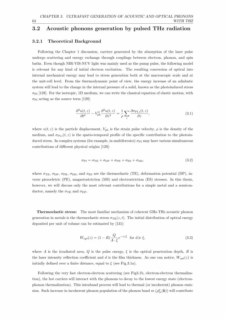
63CHAPTER 3. ULTRAFAST GENERATION OF ACOUSTIC AND OPTICAL PHONONS
WITH THZ
3.2 Acoustic phonons generation by pulsed THz radiation
3.2.1 Theoretical Background
Following the Chapter 1 discussion, carriers generated by the absorption of the laser pulseundergo scattering and energy exchange through couplings between electron, phonon, and spinbaths. Even though NIR-VIS-NUV light was mainly used as the pump pulse, the following modelis relevant for any kind of initial electron excitation. The resulting conversion of optical intointernal mechanical energy may lead to stress generation both at the macroscopic scale and atthe unit-cell level. From the thermodynamic point of view, the energy increase of an adiabaticsystem will lead to the change in the internal pressure of a solid, known as the photoinduced stressσPI [128]. For the isotropic, 1D medium, we can write the classical equation of elastic motion, withσPI acting as the source term [129]:
∂2u(t, z)∂t2
− V 2ph∂2u(t, z)∂z2 = 1
ρ
∑i
∂σPI,i(t, z)∂z
, (3.1)
where u(t, z) is the particle displacement, Vph is the strain pulse velocity, ρ is the density of themedium, and σPI,i(t, z) is the spatio-temporal profile of the specific contribution to the photoin-duced stress. In complex systems (for example, in multiferroics) σPI may have various simultaneouscontributions of different physical origins [129]:
σPI = σTE + σDP + σPE + σES + σMS, (3.2)
where σTE, σDP, σPE, σMS, and σES are the thermoelastic (TE), deformation potential (DP), in-verse piezoeletric (PE), magnetostriction (MS) and electrostriction (ES) stresses. In this thesis,however, we will discuss only the most relevant contributions for a simple metal and a semicon-ductor, namely the σTE and σDP.
Thermoelastic stress: The most familiar mechanism of coherent GHz-THz acoustic phonongeneration in metals is the thermoelastic stress σTE(z, t). The initial distribution of optical energydeposited per unit of volume can be estimated by [131]:
Wopt(z) = (1 −R) Q
A · ξe−z/ξ for d≫ ξ, (3.3)
where A is the irradiated area, Q is the pulse energy, ξ is the optical penetration depth, R isthe laser intensity reflection coefficient and d is the film thickness. As one can notice, Wopt(z) isinitially defined over a finite distance, equal to ξ (see Fig.3.1a).
Following the very fast electron-electron scattering (see Fig3.1b, electron-electron thermaliza-tion), the hot carriers will interact with the phonons to decay to the lowest energy state (electron-phonon thermalization). This intraband process will lead to thermal (or incoherent) phonon emis-sion. Such increase in incoherent phonon population of the phonon band m (ρp
m(k)) will contribute
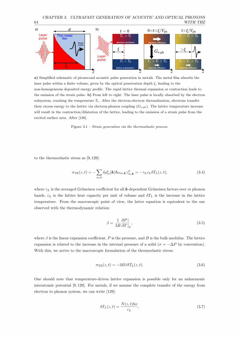
64CHAPTER 3. ULTRAFAST GENERATION OF ACOUSTIC AND OPTICAL PHONONS
WITH THZ
a) Simplified schematic of picosecond acoustic pulse generation in metals. The metal film absorbs thelaser pulse within a finite volume, given by the optical penetration depth ξ, leading to thenon-homogeneous deposited energy profile. The rapid lattice thermal expansion or contraction leads tothe emission of the strain pulse. b) From left to right: The laser pulse is locally absorbed by the electronsubsystem, reaching the temperature Te. After the electron-electron thermalization, electrons transfertheir excess energy to the lattice via electron-phonon coupling (Ge-ph). The lattice temperature increasewill result in the contraction/dilatation of the lattice, leading to the emission of a strain pulse from theexcited surface area. After [130].
Figure 3.1 – Strain generation via the thermoelastic process.
to the thermoelastic stress as [9, 129]:
σTE(z, t) = −∑m,k
δρpm(k)ℏωm,kγ
pm,k = −γLcLδTL(z, t), (3.4)
where γL is the averaged Grüneisen coefficient for all k-dependent Grüneisen factors over m phononbands, cL is the lattice heat capacity per unit of volume and δTL is the increase in the latticetemperature. From the macroscopic point of view, the latter equation is equivalent to the oneobserved with the thermodynamic relation:
β = 13B
∂P
∂T
∣∣∣∣V
, (3.5)
where β is the linear expansion coefficient, P is the pressure, and B is the bulk modulus. The latticeexpansion is related to the increase in the internal pressure of a solid (σ = −∆P by convention).With this, we arrive to the macroscopic formulation of the thermoelastic stress:
σTE(z, t) = −3BβδTL(z, t). (3.6)
One should note that temperature-driven lattice expansion is possible only for an anharmonicinteratomic potential [9, 129]. For metals, if we assume the complete transfer of the energy fromelectron to phonon system, we can write [129]:
δTL(z, t) = N(z, t)hνcL
, (3.7)
65CHAPTER 3. ULTRAFAST GENERATION OF ACOUSTIC AND OPTICAL PHONONS
WITH THZ
a) The absorption of the laser pulse leads to the electron-hole pair creation, and the change in theelectronic distribution δE. b) In turn, this shift in the electronic distribution δE modifies the interatomicinteraction which leads to the strain generation (δV/V ). c) Over bandgap excitation (ℏω > Eg) leads toboth deformation potential stress (δE) and thermal phonon emission. Adapted from [129,132].
Figure 3.2 – Band-structure picture of the deformation potential stress.
where N is the photoexcited carrier concentration and hν is the pump photon energy. In addition tothe stress generation through the lattice heating, one needs to account for the photoinduced changein the electronic distribution, i.e., deformation potential stress, resulting from the light-inducedmodification of the electron-cation interaction.
Deformation potential stress: The deformation potential stress (σDP) can be described asinteratomic potential modification due to the change in the electronic distribution. For example,the change in electronic energy in the band n by an amount δEn,k (see Fig.3.2a), may lead to thevolume change of a solid [24,129]:
δV
V
∣∣∣∣n,k
= δEn,k
dehn,k
, (3.8)
where dehn,k is the deformation potential coefficient of the energy level En,k. The change in electron-
hole distribution described by δEn,k will affect the interatomic potential. This will result in the iondisplacement and creation or annihilation of a phonon, as shown in the Fig.3.2b. The deformationpotential stress is usually expressed in terms of the light-induced modification of carrier populationδρe
n(k) at different energy levels En,k as [129]:
σDP = −∑n,k
δρen(k)En,kγ
enk =
∑n,k
δρen(k)∂En,k
∂ηn,k, (3.9)
where ηn,k is the strain generated by the change in electronic distribution, and γek is the electron
Grüneisen coefficient.
General case: In reality, both σDP and σTE can simultaneously contribute to the totalphotoinduced stress in both metals and semiconductors. In metals, the non-negligible σDP can existfor high electron temperatures. Therefore, the total photoinduced stress, as a sum of thermoelastic
66CHAPTER 3. ULTRAFAST GENERATION OF ACOUSTIC AND OPTICAL PHONONS
WITH THZ
and electronic equivalent of the phononic pressure is defined as [129,133]:
σ = σTE + σDP = −3BβδTL − γeceδTe (Metal) . (3.10)
with γe and ce the electronic Grüneisen coefficient and the electronic heat capacity.
In the semiconductor, upon the electron and hole intraband thermalization (i.e. when the elec-trons and holes are localized at the bottom or top of the conduction or valence bands, respectively),the deformation potential can be written as:
σDP = N∂Eg
∂ξ= −NB∂Eg
∂P= −Ndeh, (3.11)
where deh is the electron-hole deformation potential parameter for this particular electron-holeenergy distribution. Finally, when the incident photon energy is larger than the bandgap (ℏω > Eg,see Figure 3.2c), one should account for both the deformation potential and thermal phononcontributions [129,131]:
σ = σDP + σTE = −Ndeh − 3BβN (ℏω − Eg)cL
(Semiconductor) , (3.12)
where δTL = N(ℏω−Eg)
cLis the contribution to the heating of the lattice due to the intraband
relaxation process. Usually, linear expansion coefficient β is positive for most solids, so incoherentphonons produce negative stress. On the other hand, the sign of deh may be positive or negative(case of photoexcited silicon [134]), so the total photoinduced strain may be the sum or differenceof DP and TE contributions.
According to Eq.3.1, the non-uniform change in the internal pressure will lead to the generationof the strain pulse in the material. For the semi-infinite solids, Thomsen et al. have establishedthe expression of the bipolar strain pulse emission from a free surface [103,131]. As a first approx-imation, if there is no fast carrier or heat diffusion process, the spatial distribution of the strainpulse is limited by the optical penetration depth of the pump [128]. In that case, the characteristicfrequency of the emitted acoustic pulse is f = Vac/2ξ.
In addition, for a thin film with a thickness comparable with an optical penetration depth, asin the samples presented later, the photoinduced stress is defined over the entire film thicknessH. The thin-film geometry restricts the spatial distribution of the photoinduced stress, whichresults in filtering the phonon spectrum (Fabry-Perot cavity effect) to specific values given by theequation:
f = lVac
2H , (3.13)
with l, Vac, and H the mode number, the longitudinal speed of sound, and the film thickness,respectively. Apart from these breathing modes of the thin film, the other frequencies interferedestructively.
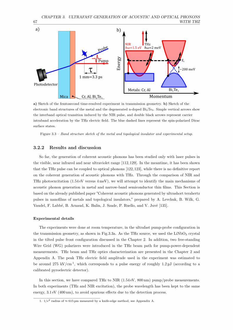
67CHAPTER 3. ULTRAFAST GENERATION OF ACOUSTIC AND OPTICAL PHONONS
WITH THZ
a) Sketch of the femtosecond time-resolved experiment in transmission geometry. b) Sketch of theelectronic band structures of the metal and the degenerated n-doped Bi2Te3. Simple vertical arrows showthe interband optical transition induced by the NIR pulse, and double black arrows represent carrierintraband acceleration by the THz electric field. The blue dashed lines represent the spin-polarized Diracsurface states.
Figure 3.3 – Band structure sketch of the metal and topological insulator and experimental setup.
3.2.2 Results and discussion
So far, the generation of coherent acoustic phonons has been studied only with laser pulses inthe visible, near infrared and near ultraviolet range [112,129]. In the meantime, it has been shownthat the THz pulse can be coupled to optical phonons [122,123], while there is no definitive reporton the coherent generation of acoustic phonons with THz. Through the comparison of NIR andTHz photoexcitation (1.54 eV versus 4 meV), we will attempt to identify the main mechanisms ofacoustic phonon generation in metal and narrow-band semiconductor thin films. This Section isbased on the already published paper "Coherent acoustic phonons generated by ultrashort terahertzpulses in nanofilms of metals and topological insulators," prepared by A. Levchuk, B. Wilk, G.Vaudel, F. Labbé, B. Arnaud, K. Balin, J. Szade, P. Ruello, and V. Juvé [135].
Experimental details
The experiments were done at room temperature, in the ultrafast pump-probe configuration inthe transmission geometry, as shown in Fig.3.3a. As the THz source, we used the LiNbO3 crystalin the tilted pulse front configuration discussed in the Chapter 2. In addition, two free-standingWire Grid (WG) polarizers were introduced in the THz beam path for pump-power-dependentmeasurements. THz beam and THz optics characterization are presented in the Chapter 2 andAppendix A. The peak THz electric field amplitude used in the experiment was estimated tobe around 275 kV/cm 1, which corresponds to a pulse energy of roughly 1.2 µJ (according to acalibrated pyroelectric detector).
In this section, we have compared THz to NIR (1.54 eV, 800 nm) pump/probe measurements.In both experiments (THz and NIR excitation), the probe wavelength has been kept to the sameenergy, 3.1 eV (400 nm), to avoid spurious effects due to the detection process.
1. 1/e2 radius of ≈ 615 µm measured by a knife-edge method, see Appendix A.
68CHAPTER 3. ULTRAFAST GENERATION OF ACOUSTIC AND OPTICAL PHONONS
WITH THZ
Samples
Chromium and Aluminum films : Thin polycrystalline films were prepared by pulsed-vapor deposition on a transparent mica substrate with the thicknesses of H = 14 ± 0.5 nm (Cr)and H = 20 ± 0.5 nm (Al) measured by x-ray reflectivity. Both deposition and x-ray reflectivityexperiments were done at the IMMM laboratory by Dr. Mathieu Edely.
Bi2Te3 thin film: Bismuth Telluride, (Bi2Te3), is a narrow-gap semiconductor (with Eg ≈0.2 eV [136]), known for its thermoelectric properties, with high electrical conductivity and low lat-tice thermal conductivity [137–139], making it appealing for industrial applications. In addition,Bi2Te3 can support unique surface conduction bands, first measured by Angle-Resolved Photoemis-sion Spectroscopy (ARPES) by Noh et al. [140], making this material a topological insulator [141].As depicted in the Fig.3.3b, topological insulators have a bulk bandgap like an ordinary insulatorand so-called surface conducting Dirac states. The topological insulator nature of Bi2Te3 arisesfrom both spin-orbit interaction (Z=83 for Bi and Z=52 for Te) and time-reversal symmetrybreaking at the interface [136]. However, in this thesis, we do not probe the topological orderof Bi2Te3. Firstly, due to the strong n-doping of the sample (see ARPES measurement of [142])the Fermi level is shifted closer to the conduction band, therefore making the manipulation ofDirac states more difficult. Secondly, the visible probe has an optical penetration depth of around9 nm [143] and is not sensitive to the surface states. The samples were grown by molecular beamepitaxy in the Physics Institute of Katowice, the University of Silesia, by Dr. K. Balin and Prof.J. Szade. As described in previous references [110,142,144,145], the sample is of high quality withsingle-crystalline growth and trigonal axis oriented perpendicular to the surface. The Bi2Te3 layerwas deposited onto the mica substrate.
Experimental results
In this part, we start first with experimental results on coherent acoustic phonon generationwith THz and NIR ultrashort pulses in prototypical metals (Chromium and Aluminum). Thesecond part will be an extension of this study to more complex materials such as topologicalinsulator Bi2Te3.
Cr and Al nanofilms: The change in the 400 nm probe beam transmission (δT (τ)/T ) asthe function of the pump-probe delay for the Cr and Al thin films are displayed in Figure 3.4aand b, with both samples showing similar transient behavior. The black line in Fig.3.4a showsthe chromium thin film δT (τ)/T signal measured upon the THz excitation with pulse energyof roughly 1.2 µJ, which corresponds to peak ETHz ≈ 275 kV cm−1. The signal consists of asharp increase in the probe transmission followed by a slower exponential decay. This exponentialdecay is attributed to the lattice temperature elevation (δTL, incoherent phonons) and subsequentheat diffusion [146–149]. On top of this thermal background, a clear oscillatory feature can beobserved. To isolate only the oscillatory component, we fit the thermal background with thefollowing function:
f(τ) = a0
·(
1 + erf[τ − τ0
s
])· a1 exp
[τ − τ0
τ1
], (3.14)
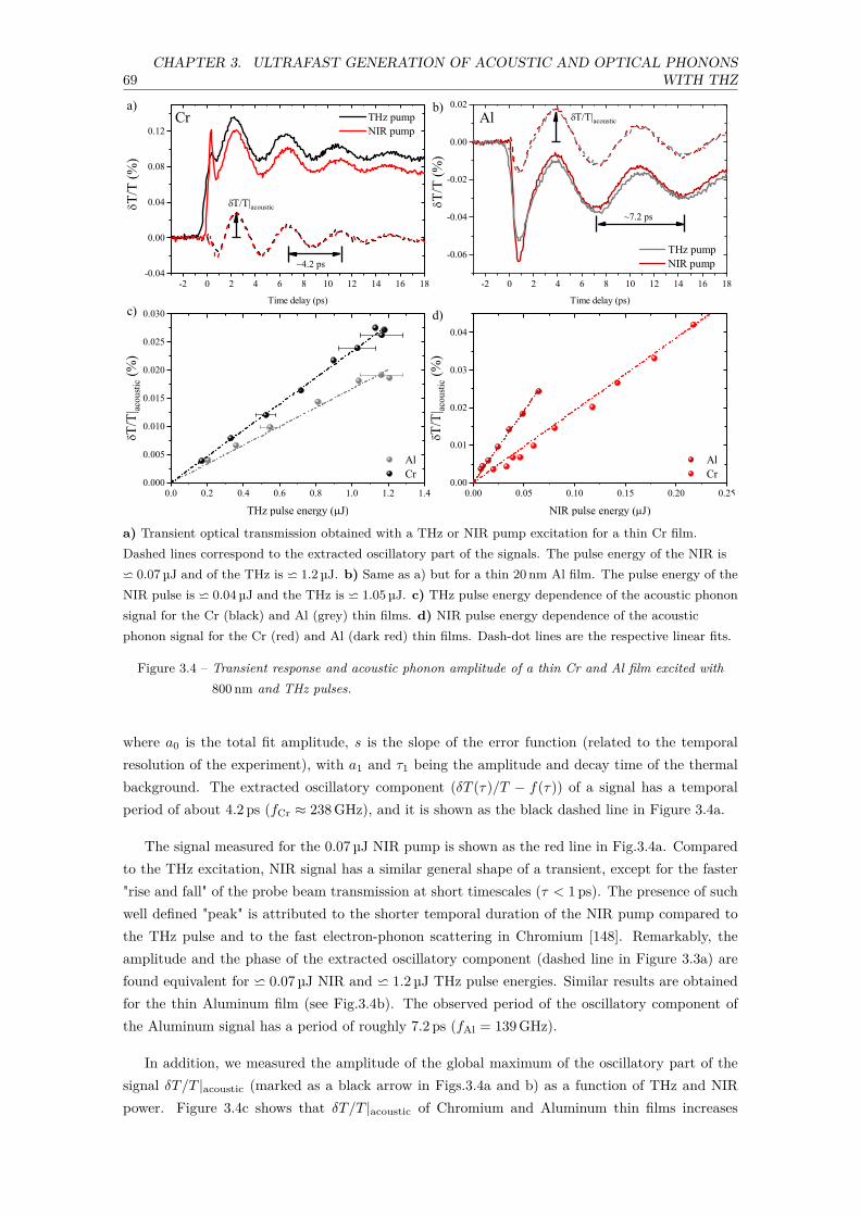
69CHAPTER 3. ULTRAFAST GENERATION OF ACOUSTIC AND OPTICAL PHONONS
WITH THZ
a) Transient optical transmission obtained with a THz or NIR pump excitation for a thin Cr film.Dashed lines correspond to the extracted oscillatory part of the signals. The pulse energy of the NIR is⋍ 0.07 µJ and of the THz is ⋍ 1.2 µJ. b) Same as a) but for a thin 20 nm Al film. The pulse energy of theNIR pulse is ⋍ 0.04 µJ and the THz is ⋍ 1.05 µJ. c) THz pulse energy dependence of the acoustic phononsignal for the Cr (black) and Al (grey) thin films. d) NIR pulse energy dependence of the acousticphonon signal for the Cr (red) and Al (dark red) thin films. Dash-dot lines are the respective linear fits.
Figure 3.4 – Transient response and acoustic phonon amplitude of a thin Cr and Al film excited with800 nm and THz pulses.
where a0 is the total fit amplitude, s is the slope of the error function (related to the temporalresolution of the experiment), with a1 and τ1 being the amplitude and decay time of the thermalbackground. The extracted oscillatory component (δT (τ)/T − f(τ)) of a signal has a temporalperiod of about 4.2 ps (fCr ≈ 238 GHz), and it is shown as the black dashed line in Figure 3.4a.
The signal measured for the 0.07 µJ NIR pump is shown as the red line in Fig.3.4a. Comparedto the THz excitation, NIR signal has a similar general shape of a transient, except for the faster"rise and fall" of the probe beam transmission at short timescales (τ < 1 ps). The presence of suchwell defined "peak" is attributed to the shorter temporal duration of the NIR pump compared tothe THz pulse and to the fast electron-phonon scattering in Chromium [148]. Remarkably, theamplitude and the phase of the extracted oscillatory component (dashed line in Figure 3.3a) arefound equivalent for ⋍ 0.07 µJ NIR and ⋍ 1.2 µJ THz pulse energies. Similar results are obtainedfor the thin Aluminum film (see Fig.3.4b). The observed period of the oscillatory component ofthe Aluminum signal has a period of roughly 7.2 ps (fAl = 139 GHz).
In addition, we measured the amplitude of the global maximum of the oscillatory part of thesignal δT/T |acoustic (marked as a black arrow in Figs.3.4a and b) as a function of THz and NIRpower. Figure 3.4c shows that δT/T |acoustic of Chromium and Aluminum thin films increases

70CHAPTER 3. ULTRAFAST GENERATION OF ACOUSTIC AND OPTICAL PHONONS
WITH THZ
a) Transient optical transmission obtained with a THz or NIR pump excitation for a 16-nm Bi2Te 3 thinfilm with 51 nJ and 1.2 µJ for NIR and THz excitation, respectively. Inset: Oscillatory part of the signal.b) THz pulse energy dependence of the acoustic phonon amplitude for the 16 nm thin film. c) Thicknessdependence of the coherent acoustic phonon signal generated by THz excitation. d) Coherent acousticphonon oscillation period vs. the film thickness.
Figure 3.5 – THz pump: Bi2Te3 thickness dependence on the coherent phonon signal.
linearly with the THz pulse energy (quadratically with the ETHz amplitude). The same lineardependence is found for the NIR pump, as depicted in Fig.3.4d.
Bi2Te3 nanofilms: As the following step, we extended our study to thin Te rich and conse-quently n-doped Bi2Te3 films with various thicknesses ranging from 4 to 25 nm. Figure 3.5a showsthe signal of Bi2Te3 16 nm film excited with THz and NIR pump pulse energy fixed at 1.2 µJ and51 nJ, respectively. For both pump wavelengths, the transient optical transmission δT/T shows asharp increase after the initial excitation and a fast recovery followed by a slower decaying signalattributed to the thermal background. We extracted the oscillatory part of the signal with a similarfit (see Eq.3.14) having two exponential decays. Fast exponential decay was found to be equal to1.8 ps, and it is related to the hot carrier relaxation [150–152].
When the thermal background is subtracted (see inset in Fig.3.5a), we observe the δT/Tresidue
modulation at two distinct frequencies: a fast oscillatory component at around 1.8 THz, which isattributed to the Raman active A1
1g optical phonon [153] (will be discussed in the Section 3.3.2) anda slower, with a period of about 11.6 ps (fBT = 86 GHz frequency). We report that the amplitude ofthe slow oscillatory component scales linearly with the THz pulse energy (see Fig. 3.5b). We thenmeasured the δT/T |residue change for Bi2Te3 films with different thicknesses, and the correspondingsignals are shown in Figure 3.5c. We see that only the frequency of a slow oscillatory component
71CHAPTER 3. ULTRAFAST GENERATION OF ACOUSTIC AND OPTICAL PHONONS
WITH THZ
is drastically affected by the change of Bi2Te3 thickness. Figure 3.5d depicts clear linear samplethickness dependence of the low frequency mode. We found the highest frequency of this mode tobe ≈ 250 GHz, measured for the 4 nm thick sample.
Discussion
Nature of the acoustic mode: In the previous sections, we have shown that THz and NIRexcitation of thin metallic and Bi2Te3 films grown on the mica substrate leads to similar transientbehavior of δT/T for the specific combination of THz and NIR pulse energies. Furthermore, theamplitude of the oscillatory part of the signal scales linearly with THz and NIR pulse energy (seeFig.3.4c and d). In addition, we show that the period of the low-frequency oscillatory componentpresent in the Bi2Te3 transient response is directly proportional to the film thickness H (seeFig.3.5d) suggesting these oscillations are the mechanical resonances of the layers.
To confirm the nature of this low-frequency δT/T modulation, we start by analysing the me-chanical boundary conditions, in order to establish which acoustic modes can be excited. We firstnote that since pump light penetration depth ξ is bigger than the film thickness H, it means thatthe photoinduced stress will be confined within the acoustic layer. Next, we estimate the acousticreflection coefficient at the metal/mica interface, defined as [128]:
Rac = Zmica − Zlayer
Zmica + Zlayer, (3.15)
where Z is the acoustic impedance :
Z = ρVac, (3.16)
with the material density ρ and the acoustic velocity Vac. With the values from the literature, theacoustic impedance of all the materials chosen as the layer here (Cr, Al, Bi2Te3) is larger thanthe acoustic impedance of the substrate 2. This leads to Rac < 0 for all interfaces. The Rac < 0value means that the acoustic wave reflected at the interface will be phase-shifted by π [128] aftera single trip, repeating each time it bounces back and forth within the acoustic layer. This leadsto the resonator-like vibration of the nanometric film at the frequency f = lVac/2H (see Eq.3.13).Then, the straightforward estimation of the eigenmode frequencies for all layers gives:
fCr = 1 · 6600 m s−1
2 · 14 nm = 235.7 GHz (Experiment: 238 GHz);
fAl = 1 · 6320 m s−1
2 · 20 nm = 158 GHz (Experiment: 139 GHz);
fBT = 1 · 2460 m s−1
2 · 16 nm = 77 GHz (Experiment: 86 GHz),
(3.17)
and they are in a rather good agreement with experimentally measured values. The about 12 %difference for the Al thin film could be related to a decrease in VAl due to polycrystalline nature ofthe film, as observed before for Mg-Zn alloy for instance [154]. For the Bi2Te3, the speed of sound
2. ρmica = 2880 kg m−3, Vmica = 4300 m s−1, Zmica = 1.2 × 10⁷ kg m−2 s−1.

72CHAPTER 3. ULTRAFAST GENERATION OF ACOUSTIC AND OPTICAL PHONONS
WITH THZ
was taken from [110, 144]. In our study, the fit of acoustic period measured with THz excitationas a function of the film thickness (red dashed line in Figure 3.5d), gives the VBT = 2700 m s−1,which deviates by less than 10 % from previous reports [155].
Acoustic phonon generation mechanism in metals: We continue the discussion withthe pump power dependence of coherent acoustic phonon amplitude, presented in Fig.3.4c andd. Importantly, for both THz and NIR excitation, δT/T |acoustic scales linearly with the pumppulse energy. This means that for all samples in the study, linearity of δT/T |acoustic for the THzexcitation excludes highly nonlinear processes of energy deposition such as impact ionization [118]or Zener tunneling [116]. With this in mind, we can now estimate the absorbed energy density inthe case of THz and NIR excitation within the usual dielectric response approach.
With the THz time-domain spectroscopy, we have first measured the complex dielectric functionof the 14 nm thick Cr film in the 0.2-2.5 THz frequency range [99], shown in Figure 3.6a. Byfitting the measured data with a simple Drude model, we extract Chromium plasma frequencyωp ≈ 350 THz and the electronic scattering rate τe ≈ 14 THz. These parameters lead to a nearly-frequency-independent 3 conductivity σCr ≈ 4.5 × 10⁵ Ω m−1. In addition, as the characteristicscattering frequency in metals is typically well above the frequency of our driving THz field [156],we limit our model to the stationary drift electron transport regime and neglect any ballistictransport effects. These two assumptions allow us to ignore the ETHz retardation effects, and wecan write the time-dependent current density associated to the electron acceleration in the presenceof the local THz pulse as:
j(t′) = σ
∫ t′
−∞Eloc
THz(t′′)dt′′. (3.18)
Here, ElocTHz(t) is the local THz electric field acting on the electrons, and σ is the frequency-
independent metal conductivity. Then, we can estimate the temporal profile of the absorbedenergy with the ultrafast analogy of the well-known Joule effect:
WAbs.THz (t) =
∫ t
−∞Eloc
THz(t′) · j(t′)dt′ = σ
∫ t
−∞
[Eloc
THz(t′)]2dt′. (3.19)
In the case of THz excitation, since our samples are much thinner than the driving field’swavelength, the local electric field can be approximated by the electric field inside the sampleEloc
THz. Prof. Brice Arnaud (Theory group at IMMM) has implemented the finite difference timedomain (FDTD) method to simulate the electric field value in the sample and the substrate:
ElocTHz(t) = s · ETHz(t), (3.20)
with ETHz(t) being the vacuum THz electric field and s ≈ 0.45 is the electric field attenuationcoefficient, estimated from FDTD.
3. Within the experimental THz frequency range.

73CHAPTER 3. ULTRAFAST GENERATION OF ACOUSTIC AND OPTICAL PHONONS
WITH THZ
a) Dielectric function of Chromium in the THz frequency range. Experimental dielectric function of theCr thin film measured by THz-TDS (dots and squares). The lines are fitted with the Drude model. b)Acoustic phonon amplitude as a function of the absorbed density energy for the Cr sample, calculatedwith Eq.3.19.
Figure 3.6 – The dielectric function of Cr and acoustic phonon amplitude in the absorbed density ofenergy for THz and NIR excitation.
Using Eq.3.19 and the experimental parameters, for the highest experimental THz field value(roughly 275 kV cm−1, pulse energy of about 1.2 µJ) we can now estimate the total absorbed energydensity, which becomes WAbs.
THz ≈ 52 J cm−3. Using the value of Chromium heat capacity from theliterature (cL ≈ 3 × 10⁶ J m−3), we can finally calculate the lattice temperature increase via theultrafast THz Joule effect:
δTL(THz) = WAbsTHzcL
≈ 17 K. (3.21)
In contrast to the THz excitation, the absorbed energy induced by NIR excitation is mediatedby the direct optical transitions, which gives:
WAbsNIR = ANℏωNIR
V, (3.22)
with A being the optical absorption coefficient, N is the number of incident photons of energyhνNIR, and the excited volume V . The NIR absorption coefficient A was modeled by the transfermatrix method using tabulated optical constants [156]. Remarkably, for the NIR pulse energy of0.07 µJ (see Fig.3.4a) we obtain an absorbed energy of WAbs
NIR ≈ 53 J cm−3, equivalent to the oneobtained with Eq.3.21, for the THz pulse energy of 1.2 µJ. Consequently, for both scenarios (NIRand THz excitation), the maximum lattice temperature increase is estimated around δTL ≈ 17 K.Figure 3.6b shows that this equivalence is valid over the entire absorbed energy range underinvestigation: the acoustic phonon amplitude is driven solely by the total absorbed energy and isnot dependent on the photon energy of the excitation pulse. This indicates that the amplitudeof the acoustic phonon is not drastically dependent on the pathway of energy relaxation from theelectron to the phonon subsystem (which is supposed to be different for a NIR and THz excitation)but only on the total absorbed energy by the lattice.
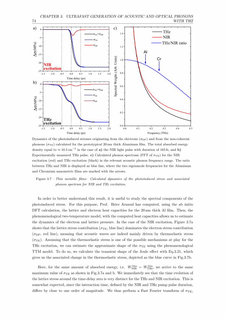
74CHAPTER 3. ULTRAFAST GENERATION OF ACOUSTIC AND OPTICAL PHONONS
WITH THZ
Dynamics of the photoinduced stresses originating from the electrons (σDP) and from the non-coherentphonons (σTE) calculated for the prototypical 20 nm thick Aluminum film. The total absorbed energydensity equal to ≈ 10 J cm−3 in the case of a) the NIR light pulse with duration of 165 fs, and b)Experimentally measured THz pulse. c) Calculated phonon spectrum (FFT of σTE) for the NIRexcitation (red) and THz excitation (black) in the relevant acoustic phonon frequency range. The ratiobetween THz and NIR is displayed as blue line, where the two eigenmode frequencies for the Aluminumand Chromium nanometric films are marked with the arrows.
Figure 3.7 – Thin metallic films: Calculated dynamics of the photoinduced stress and associatedphonon spectrum for NIR and THz excitation.
In order to better understand this result, it is useful to study the spectral components of thephotoinduced stress. For this purpose, Prof. Brice Arnaud has computed, using the ab initioDFT calculation, the lattice and electron heat capacities for the 20 nm thick Al film. Then, thephenomenological two-temperature model, with the computed heat capacities allows us to estimatethe dynamics of the electron and lattice pressure. In the case of the NIR excitation, Figure 3.7ashows that the lattice stress contribution (σTE, blue line) dominates the electron stress contribution(σDP, red line), meaning that acoustic waves are indeed mainly driven by thermoelastic stress(σTE). Assuming that the thermoelastic stress is one of the possible mechanisms at play for theTHz excitation, we can estimate the approximate shape of the σTE using the phenomenologicalTTM model. To do so, we calculate the transient shape of the Joule effect with Eq.3.21, whichgives us the associated change in the thermoelastic stress, depicted as the blue curve in Fig.3.7b.
Here, for the same amount of absorbed energy, i.e. WAbsNIR = WAbs
THz, we arrive to the samemaximum value of σTE as shown in Fig.3.7a and b. We immediately see that the time evolution ofthe lattice stress around the time-delay zero is very distinct for the THz and NIR excitation. This issomewhat expected, since the interaction time, defined by the NIR and THz pump pulse duration,differs by close to one order of magnitude. We thus perform a Fast Fourier transform of σTE,

75CHAPTER 3. ULTRAFAST GENERATION OF ACOUSTIC AND OPTICAL PHONONS
WITH THZ
and restrict ourselves to the relevant coherent acoustic phonon frequency range (up to 500 GHz),displayed in Fig.3.7c. Interestingly, we observe that the relevant ratio of the NIR and THz phononspectral components (see blue line in Fig.3.7b) is close to 1 in the region of interest. This perfectlyconfirms what we discussed before: for this rather low acoustic frequency, the more rapid latticeheating with a NIR compared to THz pulse is not important as soon as the characteristic rise ofthe σTE (either for NIR or THZ excitation) is much shorter that the acoustic phonon period ofinterest.
As a short summary, the analysis of the pump fluence dependence, the existence of the linearresponse, the presentation thermoelastic stress based on the TTM model, including the discussionof the spectrum of the photoinduced stress, strongly suggest that the lattice heating, as a result ofultrafast Joule effect, is the driving mechanism of the coherent acoustic phonon generation in thinmetallic films with THz.
Acoustic phonon generation mechanism in Bi2Te3: Concerning Bi2Te3, the linearincrease in both thermal background (not shown here) and δT/T |acoustic in the function of theTHz pulse energy strongly suggests that we can rule out highly-nonlinear light-excitation processessuch as Zener tunneling [116] and impact ionization [118] similarly to the observations we madein the previous subsection. Since the Bi2Te3 bandgap is in the order of 200 meV [157], we canexclude the multiphoton absorption and excitation process as well (Eg ≈ 50ℏΩTHz). However, itis worth to note that the recent ARPES measurements of 15 nm Bi2Te3 film revealed a non-zerosignal at the Fermi level [142] (see Fig.3.8b), and despite our sample was studied in air (passivatedsurface [142]), our Bi2Te3 could be very close to the metallic state. Moreover, we measure thenearly identical long-term residual signal (see Fig.3.5a and the inset) extracted with the samefit parameters for the THz and NIR excitation. This may indicate a similar coherent acousticphonon generation mechanism for two different pump photon energies, either originating fromthermoelastic, deformation potential stress, or a combination of two. Notably, the evolution of thephase of the coherent acoustic phonons excited in Bi2Te3 as a function of the sample thicknesses(see Fig.3.5c) might be related to differences in the driving excitation process [158] due to thechange in the electronic band structure for the thin samples with, in particular, some confinementeffects observed below around 6 nm [118,144]. Due to the complexity of electron-phonon couplingin this correlated material, these assumptions about coherent acoustic phonon generation in Bi2Te3
need to be supported with first-principle calculations.
Outlook: As a final element of discussion, it worth to tell that we can expect some potentialdifferences between NIR and THz excitation in metallic nanostructures through the thermoelasticprocess at least. As an illustration, Figure 3.8b reveals a dominating thermoelastic contributiondriven by Thz excitation within 1-2 THz range. That larger contribution from THz excitationat around 1.5 THz is directly related to the spectrum of the THz pulse. Therefore, one canimagine that THz excitation of high-frequency acoustic modes may reveal the very different natureof heating based either on intraband relaxation (with NIR excitation) or by multiple electronscattering at the Fermi level (with THz excitation). This makes it interesting to study the THzexcitation of metallic nanoparticles of various sizes, as one can tune their natural vibrations toTHz frequencies [159].
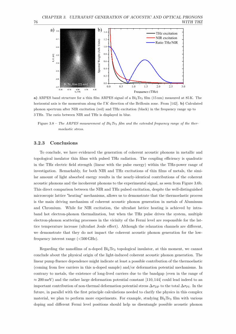
76CHAPTER 3. ULTRAFAST GENERATION OF ACOUSTIC AND OPTICAL PHONONS
WITH THZ
a) ARPES band structure for a thin film ARPES signal of a Bi2Te3 film (15 nm) measured at 85 K. Thehorizontal axis is the momentum along the ΓK direction of the Brillouin zone. From [142]. b) Calculatedphonon spectrum after NIR excitation (red) and THz excitation (black) in the frequency range up to3 THz. The ratio between NIR and THz is displayed in blue.
Figure 3.8 – The ARPES measurement of Bi2Te3 film and the extended frequency range of the ther-moelastic stress.
3.2.3 Conclusions
To conclude, we have evidenced the generation of coherent acoustic phonons in metallic andtopological insulator thin films with pulsed THz radiation. The coupling efficiency is quadraticin the THz electric field strength (linear with the pulse energy) within the THz-power range ofinvestigation. Remarkably, for both NIR and THz excitations of thin films of metals, the simi-lar amount of light absorbed energy results in the nearly-identical contributions of the coherentacoustic phonons and the incoherent phonons to the experimental signal, as seen from Figure 3.6b.This direct comparison between the NIR and THz pulsed excitation, despite the well-distinguishedmicroscopic lattice "heating" mechanisms, allows us to demonstrate that the thermoelastic processis the main driving mechanism of coherent acoustic phonon generation in metals of Aluminumand Chromium. While for NIR excitation, the ultrafast lattice heating is achieved by intra-band hot electron-phonon thermalization, but when the THz pulse drives the system, multipleelectron-phonon scattering processes in the vicinity of the Fermi level are responsible for the lat-tice temperature increase (ultrafast Joule effect). Although the relaxation channels are different,we demonstrate that they do not impact the coherent acoustic phonon generation for the low-frequency interest range (<500 GHz).
Regarding the nanofilms of n-doped Bi2Te3 topological insulator, at this moment, we cannotconclude about the physical origin of the light-induced coherent acoustic phonon generation. Thelinear pump fluence dependence might indicate at least a possible contribution of the thermoelastic(coming from free carriers in this n-doped sample) and/or deformation potential mechanisms. Incontrary to metals, the existence of long-lived carriers due to the bandgap (even in the range of≈ 200 meV) and the rather large deformation potential constant [110,144] could lead indeed to animportant contribution of non-thermal deformation potential stress ∆σDP to the total ∆σPI. In thefuture, in parallel with the first principle calculations needed to clarify the physics in this complexmaterial, we plan to perform more experiments. For example, studying Bi2Te3 film with variousdoping and different Fermi level positions should help us disentangle possible acoustic phonon
77CHAPTER 3. ULTRAFAST GENERATION OF ACOUSTIC AND OPTICAL PHONONS
WITH THZ
generation mechanisms at play. In addition, ultrafast THz experiments at low-temperature couldalso be beneficial, as they will reduce the amount of thermally activated carriers in the conductionband of Bi2Te3.
In the future, the generation of coherent acoustic phonons by an ultrashort THz pulse couldopen other fundamental opportunities for controlling the macroscopic pressure and even be used toprobe the elasticity or viscoelasticity in the soft matter. Moreover, as the new research direction inour group, the understanding of the coupling between the THz and the large internal polarizationin multiferroic materials may be crucial for the efficient control of the ferroic order.
3.3 Coherent optical phonon generation in Bi2Te3 with pulsedTHz radiation
This section will focus on the discussion about the possible mechanisms of coherent A11g optical
phonon generation in 16 nm thick Bi2Te3 film with intense THz pulses. First, we will briefly intro-duce different theoretical models of coherent optical phonon excitation with pulsed light radiation.Then, after the description of optical phonon properties of Bi2Te3 measured by Raman scatteringin general, we will present the experimental results where we will show the A1
1g mode generationefficiency dependence on ETHz field amplitude and THz pump pulse central frequency, to finallydiscuss the possible scenarios which may lead to coherent A1
1g phonon excitation.
3.3.1 Theoretical background
Phenomenologically, the motion of coherent optical phonon can be modeled as the latticeresponse on the specific driving force, usually shorter than the inverse of the coherent phononperiod of interest [160]. For example, one can use the classical equation of motion of the force-drivendamped harmonic oscillator to model the displacement of coherent phonons in the lattice [160–162]:
∂2Qα(t)∂t2
+ 2γα∂Qα(t)∂t
+ ∂V (Q)∂Qα
= FQα (t), (3.23)
where V (Q) is the total potential energy of the lattice, Qα is the normal mode coordinate 4,γα and Ωα are the phenomenological damping constant and frequency of the phonon mode α.The driving force FQ
α (t) can originate either from phonon-EM wave interaction (IR absorption orRaman scattering) or have the displacive nature due to immediate modification of the electronicdistribution [108, 163]. For example, NIR-VIS-NUV excitation of opaque materials can lead toa Displacive Excitation of Coherent Phonons (DECP), mediated by the deformation potentialstress [164].
The internal force ("harmonic and anharmonic restoring forces") is defined as the gradient of thelattice (phonon) potential energy V (Q). The V (Q) can be expressed as the polynomial expansion
4. With already included correction for the effective mass.

78CHAPTER 3. ULTRAFAST GENERATION OF ACOUSTIC AND OPTICAL PHONONS
WITH THZ
a) The difference-frequency excitation mechanisms of a coherent Raman phonon: Impulsive stimulatedRaman scattering, where ω1 − ω2 is resonant with Raman active phonon ΩR, and conventional ionicRaman scattering, leading to the shift of the Raman phonon potential. b) The sum-frequency coherentphonon excitation mechanisms: sum-frequency excitation (THz-SFE) and sum-frequency counterpart ofionic Raman scattering (THz-IRS). Adapted from [127].
Figure 3.9 – Photonic and ionic mechanisms of Raman phonon excitation.
of the all phonon modes that exist in a material, as [162,165]:
V (Q) =∑
α
Ω2α
2 Q2α +
∑α,β,γ
aαβγQαQβQγ
+∑
α,β,γ,δ
bαβγδQαQβQγQδ + . . . ,(3.24)
where the first term is the harmonic phonon potential, and other terms describe the higher-orderphonon anharmonicities (i.e., the nonlinear phonon-phonon interaction), and aαβγ and bαβγδ arethe corresponding anharmonic coefficients. The subscripts α, β, γ, etc., denote the different latticeeigenmodes. For example, when α = β = γ, cαααQ
3α is the anharmonic potential of the phonon
mode α. For α = β = γ, cααγQ2αQγ is the anharmonic coupling between phonon modes α and γ.
However, some specific anharmonic interaction terms between IR and Raman phonon modes canbe forbidden due to the crystal symmetry [2, 166].
"Conventional" phononics: stimulated IR and Raman active modes The lowest-orderallowed electric field-phonon interaction is the absorption of the EM radiation by the IR active

79CHAPTER 3. ULTRAFAST GENERATION OF ACOUSTIC AND OPTICAL PHONONS
WITH THZ
phonon mode. In this case, the IR mode equation of motion in the linear regime will read [166]:
∂2QIR(t)∂t2
+ 2γIR∂QIR(t)
∂t+ Ω2
IRQIR(t) = Z∗IRE(t), (3.25)
where Z∗IR is the effective charge of IR active mode, and E(t) is the incident electric field. A
classical example of such coupling is the phonon-polariton interaction, described in the Section1.3.1.
The lowest-order excitation of the Raman-active phonon, due to its zero effective charge (Z∗R =
0), can be mediated via the two-photon Raman process [161]. In this case, the Raman activephonon driving force is given as the second-order interaction of the electromagnetic field E andthe Raman tensor Rjk [160]:
FQR (t) = RjkEjEk, (3.26)
where Ej , Ek are the field components of the incident electromagnetic pulse. The latter equation issometimes expressed in terms of Raman polarizability tensor [161]. The Raman tensor of a givenphonon mode is defined as [165,167]:
Rjk = Vc∂χjk
∂QR, (3.27)
where χjk is the linear electric susceptibility. In this case, coherent phonon excitation is drivenby the impulsive stimulated Raman Scattering (ISRS), which is possible due to the energy andwavevector conservation rules discussed before in Chapter 1. The driven, damped equation ofmotion for the Raman active phonon will be equivalent to Eq.3.25, but with the following drivingforce [123]:
F (QR) ∝ ∂χ
∂QRE2(t). (3.28)
One should note that this force-term, proportional to E2(t), consists of both sum- and difference-frequency components of the incident electric field E(t). For example, the difference frequency com-ponents of sub-picosecond VIS-NIR pulses are linked to the ISRS excitation of coherent phononsin transparent materials (see Fig.3.9a) [106, 163, 168]. In the case of an electric field in the THzfrequency range, if the sum-frequency component is resonant with a Raman-active phonon, exci-tation can occur via photonic THz sum-frequency excitation process [123], depicted in the Figure3.9b.
Nonlinear phononics: coupled IR and Raman active modes Notably, a populationdecay of optical phonons is believed to be dominated by lattice anharmonicity and can lead to thegeneration of lower-energy acoustic and sometimes optical phonon modes [160]. About forty yearsago, it was proposed that excitation of an infrared-active phonon could serve as the intermediatestate for Raman scattering through a process that relies on lattice anharmonicities rather thansecond-order electron-phonon interactions [115,126,162]. As an example, let us expand the Eq.3.24including only one Raman QR and one IR QIR mode, taking into account only the lowest-order
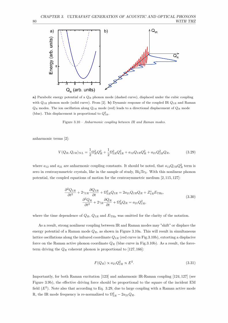
80CHAPTER 3. ULTRAFAST GENERATION OF ACOUSTIC AND OPTICAL PHONONS
WITH THZ
a) Parabolic energy potential of a QR phonon mode (dashed curve), displaced under the cubic couplingwith QIR phonon mode (solid curve). From [2]. b) Dynamic response of the coupled IR QIR and RamanQR modes. The ion oscillation along QIR mode (red) leads to a directional displacement of QR mode(blue). This displacement is proportional to Q2
IR.
Figure 3.10 – Anharmonic coupling between IR and Raman modes.
anharmonic terms [2]:
V (QR, QIR)NL = 12Ω2
RQ2R + 1
2Ω2IRQ
2IR + a12QIRQ
2R + a21Q
2IRQR, (3.29)
where a12 and a21 are anharmonic coupling constants. It should be noted, that a12QIRQ2R term is
zero in centrosymmetric crystals, like in the sample of study, Bi2Te3. With this nonlinear phononpotential, the coupled equations of motion for the centrosymmetric medium [2,115,127]:
∂2QIR
∂t2+ 2γIR
∂QIR
∂t+ Ω2
IRQIR = 2a21QIRQR + Z∗IRETHz,
∂2QR
∂t2+ 2γR
∂QR
∂t+ Ω2
RQR = a21Q2IR,
(3.30)
where the time dependence of QR, QIR and ETHz was omitted for the clarity of the notation.
As a result, strong nonlinear coupling between IR and Raman modes may "shift" or displace theenergy potential of a Raman mode QR, as shown in Figure 3.10a. This will result in simultaneouslattice oscillations along the infrared coordinate QIR (red curve in Fig.3.10b), extorting a displaciveforce on the Raman active phonon coordinate QR (blue curve in Fig.3.10b). As a result, the force-term driving the QR coherent phonon is proportional to [127,166]:
F (QR) ∝ a21Q2IR ∝ E2. (3.31)
Importantly, for both Raman excitation [123] and anharmonic IR-Raman coupling [124, 127] (seeFigure 3.9b), the effective driving force should be proportional to the square of the incident EMfield (E2). Note also that according to Eq. 3.29, due to large coupling with a Raman active modeR, the IR mode frequency is re-normalized to Ω2
IR − 2a21QR.
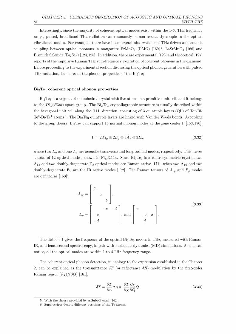
81CHAPTER 3. ULTRAFAST GENERATION OF ACOUSTIC AND OPTICAL PHONONS
WITH THZ
Interestingly, since the majority of coherent optical modes exist within the 1-40 THz frequencyrange, pulsed, broadband THz radiation can resonantly or non-resonantly couple to the opticalvibrational modes. For example, there have been several observations of THz-driven anharmoniccoupling between optical phonons in manganite PrMnO3 (PMO) [169] 5, LaSrMnO3 [166] andBismuth Selenide (Bi2Se3) [124,125]. In addition, there are experimental [123] and theoretical [127]reports of the impulsive Raman THz sum-frequency excitation of coherent phonons in the diamond.Before proceeding to the experimental section discussing the optical phonon generation with pulsedTHz radiation, let us recall the phonon properties of the Bi2Te3.
Bi2Te3 coherent optical phonon properties
Bi2Te3 is a trigonal rhombohedral crystal with five atoms in a primitive unit cell, and it belongsto the D5
3d(R3m) space group. The Bi2Te3 crystallographic structure is usually described withinthe hexagonal unit cell along the [111] direction, consisting of 3 quintuple layers (QL) of Te1-Bi-Te2-Bi-Te1 atoms 6. The Bi2Te3 quintuple layers are linked with Van der Waals bonds. Accordingto the group theory, Bi2Te3 can support 15 normal phonon modes at the zone center Γ [153,170]:
Γ = 2A1g ⊕ 2Eg ⊕ 3Au ⊕ 3Eu, (3.32)
where two Eu and one Au are acoustic transverse and longitudinal modes, respectively. This leavesa total of 12 optical modes, shown in Fig.3.11a. Since Bi2Te3 is a centrosymmetric crystal, twoA1g and two doubly-degenerate Eg optical modes are Raman active [171], when two A1u and twodoubly-degenerate Eu are the IR active modes [172]. The Raman tensors of A1g and Eg modesare defined as [153]:
A1g =
a
a
b
,
Eg =
−c −d
−c−d
, and
c
−c d
d
.(3.33)
The Table 3.1 gives the frequency of the optical Bi2Te3 modes in THz, measured with Raman,IR, and femtosecond spectroscopy, in pair with molecular dynamics (MD) simulations. As one cannotice, all the optical modes are within 1 to 4 THz frequency range.
The coherent optical phonon detection, in analogy to the expression established in the Chapter2, can be explained as the transmittance δT (or reflectance δR) modulation by the first-orderRaman tensor (∂χ)/(∂Q) [161]:
δT = ∂T
∂n∆n ≈ ∂T
∂χ
∂χ
∂QQ. (3.34)
5. With the theory provided by A.Subedi et.al. [162].6. Superscripts denote different positions of the Te atoms.

82CHAPTER 3. ULTRAFAST GENERATION OF ACOUSTIC AND OPTICAL PHONONS
WITH THZ
a) Optical phonon modes in Bi2Te3. The red and blue circles denote Te and Bi atoms, respectively.After [172]. b) Raman spectra of Bi2Te3 in backscattering geometry in parallel (VV) and crossed (VH)polarization of incident and scattered electric field, respectively. After [153].
Figure 3.11 – Sketch and Raman spectra of the optical phonon modes in the Bi2Te3.
Raman spectroscopy Femtosecond spectroscopy MD simulationMode Raman IRA1
1g 1.88 1.82 1.84A2
1g 4.02 3.91 3.74A1
1u 2.82 2.88A2
1u 3.60 3.58E1
g 1.1 1.47E2
g 3.09 3.42E1
u 1.50 1.43E2
u 2.85 2.90Subscripts u and g correspond to the Raman (in-plane) and IR (out-of-plane) lattice vibration modes,respectively. After [170–172].
Table 3.1 – Bi2Te3 optical phonon frequencies in THz.
Figure 3.11b displays the Raman spectra of Bi2Te3 crystal, showing that one can probe specificmodes selectively via polarization analysis of the probe pulse [160]. For example, modes containingonly diagonal terms (A1g) will only cause intensity modulation of the transmitted or scattered lightand therefore they are absent in depolarized spectrum in Figure 3.11b. However, modes containingoff-diagonal tensor terms (Eg) will only affect the polarization state of the scattered or transmittedlight, which, ideally, can be probed only by the polarization sensitive anisotropic detection.
3.3.2 Results and discussion
Experimental results
Before discussing the experimental results on coherent optical phonon generation with THzpulses in 16 nm thick Bi2Te3 film, let us first define the time delay zero of the experiment. For

83CHAPTER 3. ULTRAFAST GENERATION OF ACOUSTIC AND OPTICAL PHONONS
WITH THZ
a) Electrooptic trace of the THz pulse, and its fit by Eq.3.35. b) Experimental signal in THzpump-400 nm probe of the Bi2Te3 16 nm thin film at τ < 2 ps time scale (black curve). The signal isoverlapped with squared THz electric field (dash dot red) and the THz absorbed energy (dash dot blue).
Figure 3.12 – Bi2Te3 THz pump/400 nm probe: Time-delay zero definition.
this, we first fit the electrooptic trace of ETHz of the LiNbO3 source 7 with the following equation:
ETHz(τ) = E0 exp[− 4 ln 2τ2
σ2FWHM
]sin[Ω0τ + ϕ0], (3.35)
where E0 is the value of the peak electric field, σFWHM is the pulse width at FWHM, Ω0 is theangular THz central frequency, and ϕ0 is the carrier-envelope phase (CEP). Figure 3.12a showsthe THz pulse waveform ETHz(τ) (line-dot) and its fit (solid line) with the following parameters:σFWHM = 1.317 ps, E0 ≈ 275 kV cm−1, Ω0/2π = 0.64 THz and ϕ0 = 0.12π. Next, with the Eq.3.19we can calculate the approximate shape of Wabs(τ):
Wabs(τ) ∝∫ τ
−∞E2
THz(t′)dt′. (3.36)
Both E2THz(τ) and calculated Wabs(τ) are shown in the Fig.3.12b (blue and red dash-dot lines,
respectively). In this case, Bi2Te3 conductivity in the THz range, electron-electron, and electron-phonon scattering rates, that all may affect the shape of Wabs(τ) were not taken into account.In particular, such calculation of Wabs assumes an immediate dissipation of the electromagneticenergy. Finally, we manually superpose the measured signal δT/T with calculated Wabs(τ) profileas shown in the Fig.3.12b, which gives us the time-delay zero position of the experiment.
In the following, we will focus only on the optical phonon part of the signal, extracted by fittingthe acoustic mode, electronic and thermal background with the following function:
δT/T |bg =A ·(
1 + erf[τs
])·a1 exp
[− τ
τ1
]+ a2 exp
[− τ
τ2
]+
+ aaccos[Ωac(τ) + ϕac] exp[− τ
τac
],
(3.37)
7. Deconvoluted from the detection crystal response.
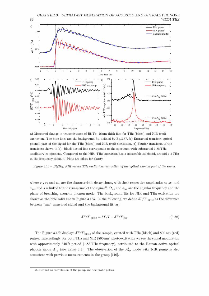
84CHAPTER 3. ULTRAFAST GENERATION OF ACOUSTIC AND OPTICAL PHONONS
WITH THZ
a) Measured change in transmittance of Bi2Te3 16 nm thick film for THz (black) and NIR (red)excitation. The blue lines are the background fit, defined by Eq.3.37. b) Extracted transient opticalphonon part of the signal for the THz (black) and NIR (red) excitation. c) Fourier transform of thetransients shown in b). Black dotted line corresponds to the spectrum with subtracted 1.85 THzoscillatory component. Compared to the NIR, THz excitation has a noticeable sideband, around 1.5 THzin the frequency domain. Plots are offset for clarity.
Figure 3.13 – Bi2Te3, NIR versus THz excitation: extraction of the optical phonon part of the signal.
where τ1, τ2 and τac are the characteristic decay times, with their respective amplitudes a1 ,a2 andaac, and s is linked to the rising-time of the signal 8. Ωac and ϕac are the angular frequency and thephase of breathing acoustic phonon mode. The background fits for NIR and THz excitation areshown as the blue solid line in Figure 3.13a. In the following, we define δT/T |optic as the differencebetween "raw" measured signal and the background fit, as:
δT/T |optic = δT/T − δT/T |bg. (3.38)
The Figure 3.13b displays δT/T |optic of the sample, excited with THz (black) and 800 nm (red)pulses. Interestingly, for both THz and NIR (800 nm) photoexcitation we see the signal modulationwith approximately 540 fs period (1.85 THz frequency), attributed to the Raman active opticalphonon mode A1
1g (see Table 3.1). The observation of the A11g mode with NIR pump is also
consistent with previous measurements in the group [110].
8. Defined as convolution of the pump and the probe pulses.
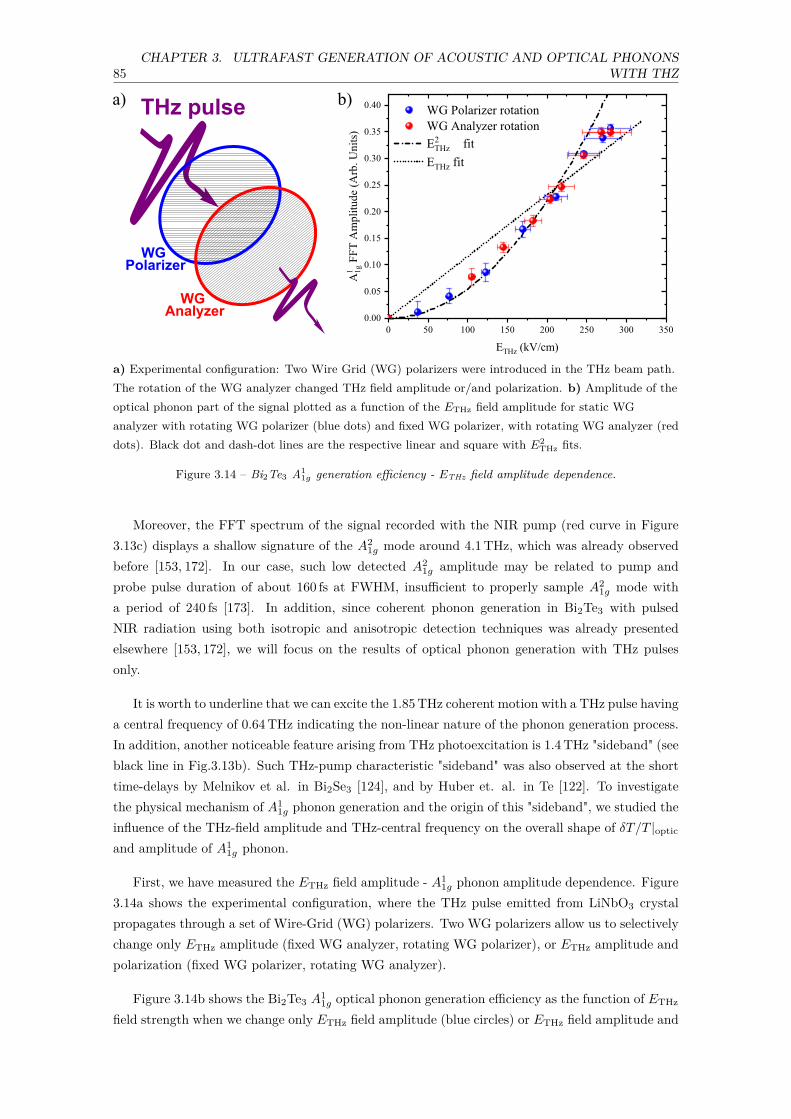
85CHAPTER 3. ULTRAFAST GENERATION OF ACOUSTIC AND OPTICAL PHONONS
WITH THZ
a) Experimental configuration: Two Wire Grid (WG) polarizers were introduced in the THz beam path.The rotation of the WG analyzer changed THz field amplitude or/and polarization. b) Amplitude of theoptical phonon part of the signal plotted as a function of the ETHz field amplitude for static WGanalyzer with rotating WG polarizer (blue dots) and fixed WG polarizer, with rotating WG analyzer (reddots). Black dot and dash-dot lines are the respective linear and square with E2
THz fits.
Figure 3.14 – Bi2Te3 A11g generation efficiency - ETHz field amplitude dependence.
Moreover, the FFT spectrum of the signal recorded with the NIR pump (red curve in Figure3.13c) displays a shallow signature of the A2
1g mode around 4.1 THz, which was already observedbefore [153, 172]. In our case, such low detected A2
1g amplitude may be related to pump andprobe pulse duration of about 160 fs at FWHM, insufficient to properly sample A2
1g mode witha period of 240 fs [173]. In addition, since coherent phonon generation in Bi2Te3 with pulsedNIR radiation using both isotropic and anisotropic detection techniques was already presentedelsewhere [153, 172], we will focus on the results of optical phonon generation with THz pulsesonly.
It is worth to underline that we can excite the 1.85 THz coherent motion with a THz pulse havinga central frequency of 0.64 THz indicating the non-linear nature of the phonon generation process.In addition, another noticeable feature arising from THz photoexcitation is 1.4 THz "sideband" (seeblack line in Fig.3.13b). Such THz-pump characteristic "sideband" was also observed at the shorttime-delays by Melnikov et al. in Bi2Se3 [124], and by Huber et. al. in Te [122]. To investigatethe physical mechanism of A1
1g phonon generation and the origin of this "sideband", we studied theinfluence of the THz-field amplitude and THz-central frequency on the overall shape of δT/T |optic
and amplitude of A11g phonon.
First, we have measured the ETHz field amplitude - A11g phonon amplitude dependence. Figure
3.14a shows the experimental configuration, where the THz pulse emitted from LiNbO3 crystalpropagates through a set of Wire-Grid (WG) polarizers. Two WG polarizers allow us to selectivelychange only ETHz amplitude (fixed WG analyzer, rotating WG polarizer), or ETHz amplitude andpolarization (fixed WG polarizer, rotating WG analyzer).
Figure 3.14b shows the Bi2Te3 A11g optical phonon generation efficiency as the function of ETHz
field strength when we change only ETHz field amplitude (blue circles) or ETHz field amplitude and
86CHAPTER 3. ULTRAFAST GENERATION OF ACOUSTIC AND OPTICAL PHONONS
WITH THZ
a) Optical phonon part of the signal recorded for the THz pump with indicated THz central frequencyΩ0/2π, and b) it is Fourier transform. Dashed-dot line is the FFT for time-delays > 1 ps. Thepurple-filled area is the respective spectrum of the THz pump pulse. Data are offset for clarity. c)Normalized to 1 amplitude of the A1
1g mode as the function of the THz central frequency Ω0/2π. d)Normalized to 1 THz power measured with the calibrated pyroelectric detector.
Figure 3.15 – Bi2Te3: Influence of the THz pump spectrum on the optical phonon part of the signal.
polarization (red circles). The error bars are set to ±10 % of the estimated value of peak ETHz9.
As seen from Figure 3.14b, two measurements overlap perfectly, meaning that A11g amplitude does
not depend on the THz pump polarization. This finding is in good agreement with previous reports[153]. In addition, A1
1g amplitude scales with the square of the THz field (δT/T |optic ∝ E2THz),
underlining the nonlinear mechanism of this Raman active excitation.
Next, we recorded the δT/T |optic for slightly different ETHz pump spectrum. In order totune the THz central frequency Ω0/2π from ≈ 0.52 and up to ≈ 0.73 THz, we have used thex-cut Quartz plate, as discussed in the Section 2.5. Figure 3.15a shows measured signals forΩ0/2π = 0.52, 0.63 and 0.73 THz. We see that both amplitude of A1
1g phonon and signal aroundτ = 0 is strongly affected by the ETHz change in Ω0/2π.
The Fig. 3.15b displays the FFT δT/T |optic signals discussed above. We observe that both A11g
amplitude and characteristic to THz excitation "sideband" are strongly correlated to the incidentETHz spectrum (violet dashed line in Figure 3.15b). This sideband seems to be related to the sum-frequency component of ETHz and completely disappears when the FFT is performed on the signalfor > 1 ps time delays (see dash-dot lines in Fig. 3.15b) [122]. Indeed, as presented in AppendixB, we find the correlation between the "sideband" and ETHz SF component for all signals recorded
9. Related to the discrepancy in the values measured with calibrated pyrodetector and THz-TDS.
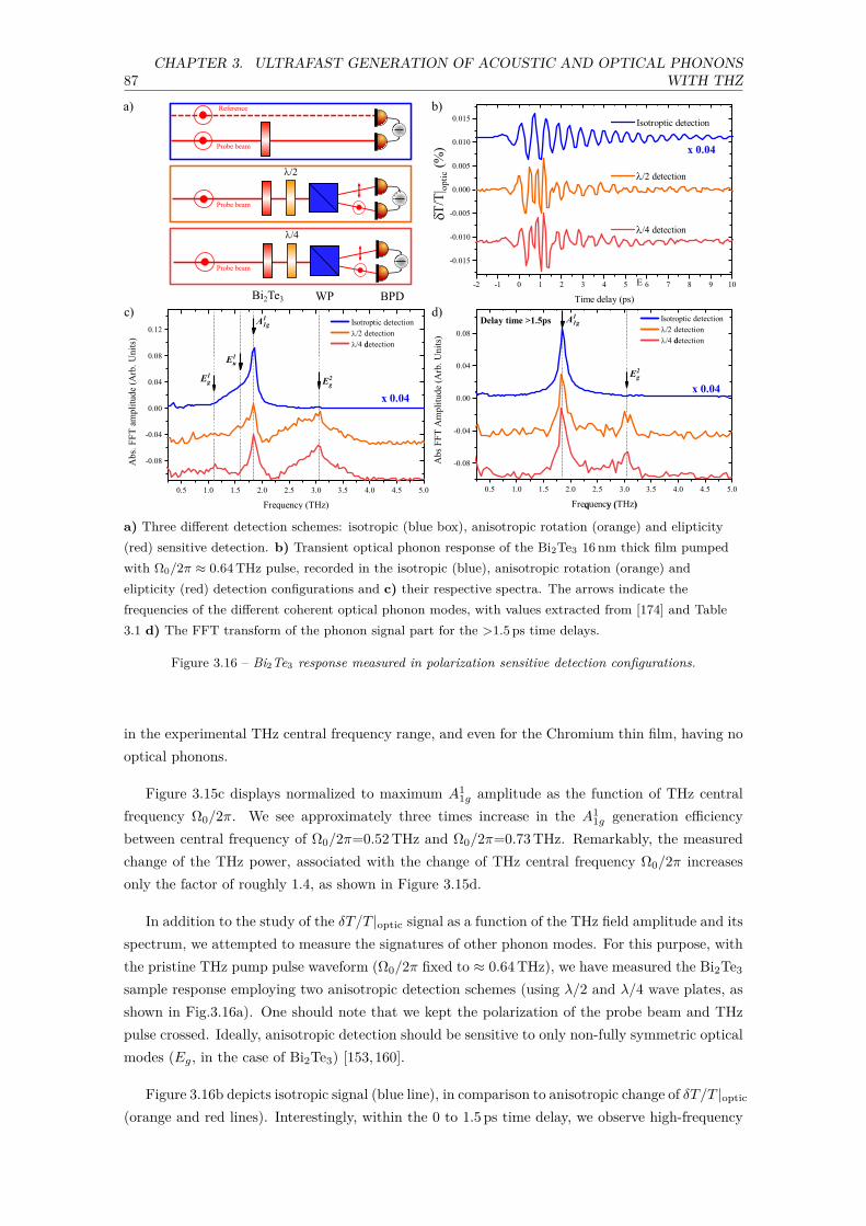
87CHAPTER 3. ULTRAFAST GENERATION OF ACOUSTIC AND OPTICAL PHONONS
WITH THZ
a) Three different detection schemes: isotropic (blue box), anisotropic rotation (orange) and elipticity(red) sensitive detection. b) Transient optical phonon response of the Bi2Te3 16 nm thick film pumpedwith Ω0/2π ≈ 0.64 THz pulse, recorded in the isotropic (blue), anisotropic rotation (orange) andelipticity (red) detection configurations and c) their respective spectra. The arrows indicate thefrequencies of the different coherent optical phonon modes, with values extracted from [174] and Table3.1 d) The FFT transform of the phonon signal part for the >1.5 ps time delays.
Figure 3.16 – Bi2Te3 response measured in polarization sensitive detection configurations.
in the experimental THz central frequency range, and even for the Chromium thin film, having nooptical phonons.
Figure 3.15c displays normalized to maximum A11g amplitude as the function of THz central
frequency Ω0/2π. We see approximately three times increase in the A11g generation efficiency
between central frequency of Ω0/2π=0.52 THz and Ω0/2π=0.73 THz. Remarkably, the measuredchange of the THz power, associated with the change of THz central frequency Ω0/2π increasesonly the factor of roughly 1.4, as shown in Figure 3.15d.
In addition to the study of the δT/T |optic signal as a function of the THz field amplitude and itsspectrum, we attempted to measure the signatures of other phonon modes. For this purpose, withthe pristine THz pump pulse waveform (Ω0/2π fixed to ≈ 0.64 THz), we have measured the Bi2Te3
sample response employing two anisotropic detection schemes (using λ/2 and λ/4 wave plates, asshown in Fig.3.16a). One should note that we kept the polarization of the probe beam and THzpulse crossed. Ideally, anisotropic detection should be sensitive to only non-fully symmetric opticalmodes (Eg, in the case of Bi2Te3) [153,160].
Figure 3.16b depicts isotropic signal (blue line), in comparison to anisotropic change of δT/T |optic
(orange and red lines). Interestingly, within the 0 to 1.5 ps time delay, we observe high-frequency
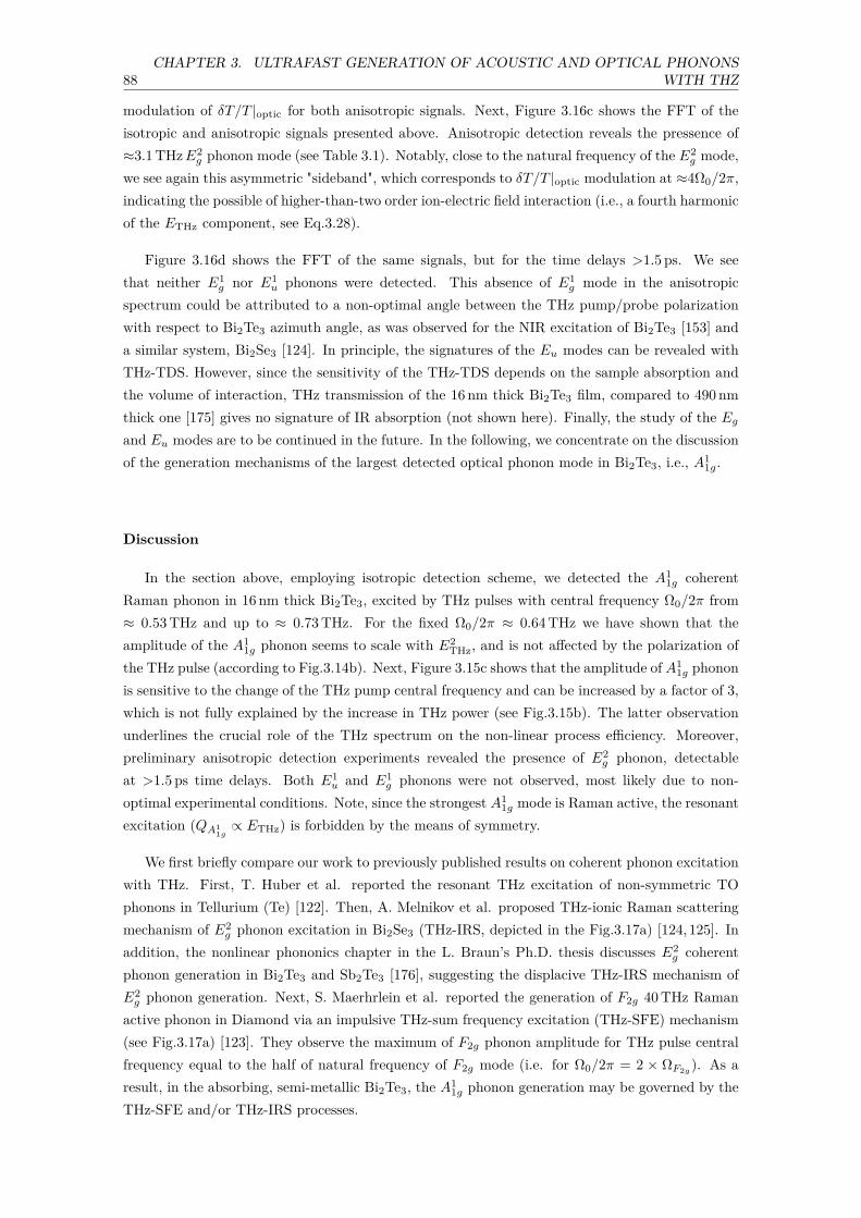
88CHAPTER 3. ULTRAFAST GENERATION OF ACOUSTIC AND OPTICAL PHONONS
WITH THZ
modulation of δT/T |optic for both anisotropic signals. Next, Figure 3.16c shows the FFT of theisotropic and anisotropic signals presented above. Anisotropic detection reveals the pressence of≈3.1 THzE2
g phonon mode (see Table 3.1). Notably, close to the natural frequency of the E2g mode,
we see again this asymmetric "sideband", which corresponds to δT/T |optic modulation at ≈4Ω0/2π,indicating the possible of higher-than-two order ion-electric field interaction (i.e., a fourth harmonicof the ETHz component, see Eq.3.28).
Figure 3.16d shows the FFT of the same signals, but for the time delays >1.5 ps. We seethat neither E1
g nor E1u phonons were detected. This absence of E1
g mode in the anisotropicspectrum could be attributed to a non-optimal angle between the THz pump/probe polarizationwith respect to Bi2Te3 azimuth angle, as was observed for the NIR excitation of Bi2Te3 [153] anda similar system, Bi2Se3 [124]. In principle, the signatures of the Eu modes can be revealed withTHz-TDS. However, since the sensitivity of the THz-TDS depends on the sample absorption andthe volume of interaction, THz transmission of the 16 nm thick Bi2Te3 film, compared to 490 nmthick one [175] gives no signature of IR absorption (not shown here). Finally, the study of the Eg
and Eu modes are to be continued in the future. In the following, we concentrate on the discussionof the generation mechanisms of the largest detected optical phonon mode in Bi2Te3, i.e., A1
1g.
Discussion
In the section above, employing isotropic detection scheme, we detected the A11g coherent
Raman phonon in 16 nm thick Bi2Te3, excited by THz pulses with central frequency Ω0/2π from≈ 0.53 THz and up to ≈ 0.73 THz. For the fixed Ω0/2π ≈ 0.64 THz we have shown that theamplitude of the A1
1g phonon seems to scale with E2THz, and is not affected by the polarization of
the THz pulse (according to Fig.3.14b). Next, Figure 3.15c shows that the amplitude of A11g phonon
is sensitive to the change of the THz pump central frequency and can be increased by a factor of 3,which is not fully explained by the increase in THz power (see Fig.3.15b). The latter observationunderlines the crucial role of the THz spectrum on the non-linear process efficiency. Moreover,preliminary anisotropic detection experiments revealed the presence of E2
g phonon, detectableat >1.5 ps time delays. Both E1
u and E1g phonons were not observed, most likely due to non-
optimal experimental conditions. Note, since the strongest A11g mode is Raman active, the resonant
excitation (QA11g
∝ ETHz) is forbidden by the means of symmetry.
We first briefly compare our work to previously published results on coherent phonon excitationwith THz. First, T. Huber et al. reported the resonant THz excitation of non-symmetric TOphonons in Tellurium (Te) [122]. Then, A. Melnikov et al. proposed THz-ionic Raman scatteringmechanism of E2
g phonon excitation in Bi2Se3 (THz-IRS, depicted in the Fig.3.17a) [124, 125]. Inaddition, the nonlinear phononics chapter in the L. Braun’s Ph.D. thesis discusses E2
g coherentphonon generation in Bi2Te3 and Sb2Te3 [176], suggesting the displacive THz-IRS mechanism ofE2
g phonon generation. Next, S. Maerhrlein et al. reported the generation of F2g 40 THz Ramanactive phonon in Diamond via an impulsive THz-sum frequency excitation (THz-SFE) mechanism(see Fig.3.17a) [123]. They observe the maximum of F2g phonon amplitude for THz pulse centralfrequency equal to the half of natural frequency of F2g mode (i.e. for Ω0/2π = 2 × ΩF2g
). As aresult, in the absorbing, semi-metallic Bi2Te3, the A1
1g phonon generation may be governed by theTHz-SFE and/or THz-IRS processes.
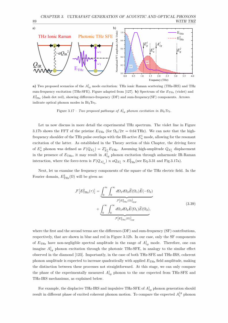
89CHAPTER 3. ULTRAFAST GENERATION OF ACOUSTIC AND OPTICAL PHONONS
WITH THZ
a) Two proposed scenarios of the A11g mode excitation: THz ionic Raman scattering (THz-IRS) and THz
sum-frequency excitation (THz-SFE). Figure adapted from [127]. b) Spectrum of the ETHz (violet) andE2
THz (dash dot red), showing difference-frequency (DF) and sum-frequency(SF) components. Arrowsindicate optical phonon modes in Bi2Te3.
Figure 3.17 – Two proposed pathways of A11g phonon excitation in Bi2Te3.
Let us now discuss in more detail the experimental THz spectrum. The violet line in Figure3.17b shows the FFT of the pristine ETHz (for Ω0/2π = 0.64 THz). We can note that the high-frequency shoulder of the THz pulse overlaps with the IR-active E1
u mode, allowing for the resonantexcitation of the latter. As established in the Theory section of this Chapter, the driving forceof E1
u phonon was defined as F (QE1u) = Z∗
E1uETHz. Assuming high-amplitude QE1
udisplacement
in the presence of ETHz, it may result in A11g phonon excitation through anharmonic IR-Raman
interaction, where the force-term is F (QA11g
) ∝ aQE1u
∝ E2THz(see Eq.3.31 and Fig.3.17a).
Next, let us examine the frequency components of the square of the THz electric field. In theFourier domain, E2
THz(Ω) will be given as:
F[E2
THz(τ)]
=∫ ∞
0
∫ ∞
0dΩ1dΩ2E(Ω1)E(−Ω2)︸ ︷︷ ︸F[E2
THz(Ω)]DF
+∫ ∞
0
∫ ∞
0dΩ1dΩ2E(Ω1)E(Ω2)︸ ︷︷ ︸F[E2
THz(Ω)]SF
,
(3.39)
where the first and the second terms are the difference-(DF) and sum-frequency (SF) contributions,respectively, that are shown in blue and red in Figure 3.12b. In our case, only the SF componentsof ETHz have non-negligible spectral amplitude in the range of A1
1g mode. Therefore, one canimagine A1
1g phonon excitation through the photonic THz-SFE, in analogy to the similar effectobserved in the diamond [123]. Importantly, in the case of both THz-SFE and THz-IRS, coherentphonon amplitude is expected to increase quadratically with applied ETHz field amplitude, makingthe distinction between these processes not straightforward. At this stage, we can only comparethe phase of the experimentally measured A1
1g phonon to the one expected from THz-SFE andTHz-IRS mechanisms, as explained below.
For example, the displacive THz-IRS and impulsive THz-SFE of A11g phonon generation should
result in different phase of excited coherent phonon motion. To compare the expected A1g1 phonon
90CHAPTER 3. ULTRAFAST GENERATION OF ACOUSTIC AND OPTICAL PHONONS
WITH THZ
phase as a result of THz-IRS and THz-SFE mechanisms, we phenomenologically solve the two setsof the differential equations describing the two distinct pathways of A1
1g excitation. However, sincewe do not have any information about the values of frequency-dependent Raman tensor R(Ω),the life-time of IR E1
u mode, its effective charge Z∗E1
u, and strength of the anharmonic interaction
between E1u and A1
1g mode, the further discussion is based on simple numerical modeling. Thesecrucial parameters and the likelihood of THz-SFE and THz-IRS processes are yet to be confirmedby the first-principle calculations.
Despite the absence of the theoretical parameters, we still able to numerically solve the set ofdifferential equations for QA1
1gdisplacement. For the THz-IRS, based on Eq.3.29 we write:
QE1u
+ 2γE1uQE1
u+ Ω2
E1uQE1
u= 2aQE1
uQA1
1g+ Z∗
E1uETHz,
QA11g
+ 2γA11gQA1
1g+ Ω2
A11gQA1
1g= aQ2
E1u,
(3.40)
where a is the anharmonic coupling coefficient, γE1u, and γA1
1gare the IR and Raman damping
constants, and Z∗E1
uis the effective charge of the E1
u mode. For ETHz, we used the experimentalTHz pulse shown in Fig.3.12a. The γA1
1gwas set to 0.285 ps−1, and it corresponds to A1
1g phonondamping time of 3.5 ps, extracted from fitting the experimental data. We set Z∗
E1u
= −1, a = −1, 10
and γE1u
= 1 ps−1. The frequency of the E1u mode (ΩE1
u= 1.5 THz) was taken from Table 3.1. The
solution for QA11g
, normalized to match the experimental data, and the driving force ∝ aQ2E1
uare
shown in the Figure 3.18a (as red line and pink filled area, respectively).
In the case of THz-SFE, one can write the following equation of motion [127,177]:
QA11g
+ 2γA11gQA1
1g+ Ω2
A11gQA1
1g= RE2
THz. (3.41)
Here, we disregard the frequency dependence of the Raman tensor and set it to unity (R = 1). Weuse the same shape of ETHz as in the THz-IRS model. Solution for QA1
1galong with its driving
force ∝ E2THz are shown in the Figure 3.18a (as orange line and filled red area, respectively).
Now, let us compare the experimental data and QA11g
displacement calculated with two modelsproposed above. Figure 3.18a compares the around time-delay zero experimental signal and solu-tions of the two models. Especially for the negative time delays, we see the big difference betweenthe δT/T |optic (black line) and calculated QA1
1gdisplacement for both THz-IRS (red line) and THz-
SFE (orange line). We believe this is because we model only part of the signal ∝ χQA1
1g
QA11g
. In
addition, "parasitic" ETHz and E2THz contributions may be present in the "raw" δT/T experimental
signal [123,178], that are not included in our simple model.
From Figure 3.18c, we see that the THz-SFE model (orange line) describes better the phase ofthe experimental signal (black line). However, it should be noted that both γE1
udamping constant
and an anharmonic coefficient a used in the THz-IRS model heavily alter the phase of QA11g
displacement, making this comparison inconclusive. As a result, there is always an open questionabout the time delay zero definition (see Fig.3.12b), making the direct experiment-simulationphonon phase comparison quite a delicate task.
10. The minus was chosen to better match the phase of experimentally measured A11g phonon.

91CHAPTER 3. ULTRAFAST GENERATION OF ACOUSTIC AND OPTICAL PHONONS
WITH THZ
a) Comparison between the experimentally measured signal (black ) curve, THz-IRS (red curve) andTHz-SFE (orange) models, with their respective driving forces shown around the time-delay zero (shadedcolor lines). b) Temporal overlap between the experimental ETHz, and modeled Q2
E1u
with E2THz. c)
δT/T |optic versus QA11g
displacement calculated with THz-IRS and THz-SFE models at the > 2 ps timedelays.
Figure 3.18 – Two proposed models of A11g phonon excitation: experiment vs. phenomenological mod-
eling.
As a final step, using the same numerical modeling, we can calculate the effect of the ETHz pumpcentral frequency on the A1
1g phonon amplitude for both THz-IRS and THz-SFE mechanisms. Fig-ure 3.19a displays the experimental data (blue circles, presented in Fig.3.15c) superimposed withthe results of the THz-IRS and THz-SFE models. Surprisingly, we have a good agreement betweenthe experiment and each proposed pathway of A1
1g phonon generation. In addition, we see that themaximum of QA1
1gdisplacement is expected for the THz central frequency of Ω0/2π = 0.925 THz
(half of A11g phonon mode natural frequency), which is out of reach in current experimental condi-
tions. Finally, at this stage, without first-principle calculations, we can not assign the generationof A1
1g phonon in 16 nm thick n-doped Bi2Te3 to either THz-SFE or THz-IRS.
3.3.3 Conclusion
In this section, we have demonstrated the excitation of A11g coherent optical phonon in Bi2Te3
with THz pulsed radiation. We show that the generation efficiency of the A11g phonon scales
quadratically with THz field amplitude, and is affected by the change in the THz central fre-quency. We have compared the experimental results to the two recently-proposed models of A1
1g
phonon excitation, namely impulsive THz-SFE and displacive THz-IRS. Given our time-delay zerodefinition, defined as the temporal overlap between the "raw" δT/T signal and calculated W abs
THz
profile, we find that the THz-SFE model does a better job in matching the experimental phase of
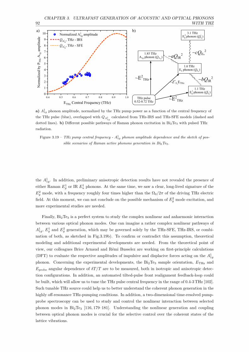
92CHAPTER 3. ULTRAFAST GENERATION OF ACOUSTIC AND OPTICAL PHONONS
WITH THZ
a) A11g phonon amplitude, normalized by the THz pump power as a function of the central frequency of
the THz pulse (blue), overlapped with QA11g
calculated from THz-IRS and THz-SFE models (dashed anddotted lines). b) Different possible pathways of Raman phonon excitation in Bi2Te3 with pulsed THzradiation.
Figure 3.19 – THz pump central frequency - A11g phonon amplitude dependence and the sketch of pos-
sible scenarios of Raman active phonons generation in Bi2Te3.
the A11g. In addition, preliminary anisotropic detection results have not revealed the presence of
either Raman E1g or IR E1
u phonons. At the same time, we saw a clear, long-lived signature of theE2
g mode, with a frequency roughly four times higher than the Ω0/2π of the driving THz electricfield. At this moment, we can not conclude on the possible mechanism of E2
g mode excitation, andmore experimental studies are needed.
Finally, Bi2Te3 is a perfect system to study the complex nonlinear and anharmonic interactionbetween various optical phonon modes. One can imagine a rather complex nonlinear pathways ofA1
1g, E1g and E2
g generation, which may be governed solely by the THz-SFE, THz-IRS, or combi-nation of both, as sketched in Fig.3.19b). To confirm or contradict this assumption, theoreticalmodeling and additional experimental developments are needed. From the theoretical point ofview, our colleagues Brice Arnaud and Rémi Busselez are working on first-principle calculations(DFT) to evaluate the respective amplitudes of impulsive and displacive forces acting on the A1
1g
phonon. Concerning the experimental developments, the Bi2Te3 sample orientation, ETHz andEprobe angular dependence of δT/T are to be measured, both in isotropic and anisotropic detec-tion configurations. In addition, an automated tilted-pulse front realignment feedback-loop couldbe built, which will allow us to tune the THz pulse central frequency in the range of 0.4-3 THz [102].Such tunable THz source could help us to better understand the coherent phonon generation in thehighly off-resonance THz-pumping conditions. In addition, a two-dimensional time-resolved pump-probe spectroscopy can be used to study and control the nonlinear interaction between selectedphonon modes in Bi2Te3 [116, 179–181]. Understanding the nonlinear generation and couplingbetween optical phonon modes is crucial for the selective control over the coherent states of thelattice vibrations.
93CHAPTER 3. ULTRAFAST GENERATION OF ACOUSTIC AND OPTICAL PHONONS
WITH THZ
3.4 Conclusions and perspectives
This chapter demonstrates the generation of coherent acoustic phonons with THz pulses innanometric films of metals (Chromium and Aluminum) and narrow-band semiconductor (BismuthTelluride) with pulsed THz radiation. We show that the coherent acoustic phonon amplitudein Cr, Al, and Bi2Te3 nanofilms scale linearly with the THz pump pulse energy. In addition,the acoustic period is proportional to the thin film thickness, as demonstrated for the Bi2Te3
nanofilms. We conclude that the THz excitation leads to the ultrafast change in the thermoelasticstress due to the ultrafast Joule effect for the Cr and Al nanofilms. In comparison, while theTHz-induced thermoelastic stress is the primary driving acoustic phonon generation mechanismin metals, the Bi2Te3’s linear acoustic response as a function of the THz-pulse energy could bea preliminary indication of a thermoelastic and/or a deformation potential generation process.However, more controlled experiments and first-principle calculations are needed to determine theorigin of coherent acoustic phonon generation with pulsed THz radiation in Bi2Te3.
In the second part of this chapter, we conduct the experimental study of coherent opticalphonon generation in 16 nm thick Bi2Te3 film with pulsed THz radiation. For the first time, wedemonstrate that the A1
1g Raman active optical phonon with 1.85 THz frequency can be excitedwith a THz pulse of a 0.64 THz central frequency. Furthermore, we show that the amplitude of theA1
1g mode scales quadratically with the amplitude of the applied THz electric field and does notdepend on the THz pump polarization. In addition, we show that the change of the THz pumpcentral frequency from 0.52 THz to 0.73 THz leads to the three times more efficient generation ofthe A1
1g phonon. We then compare the experimental data with the two phenomenological models:impulsive Raman THz-Sum Frequency excitation and displacive anharmonic THz-Ionic Ramanscattering. We find that the phase of the THz-Sum Frequency excitation model fits better thephase of experimental A1
1g signal. However, first-principle calculations are necessary to estimatethe relative amplitudes of displacive and impulsive forces that can contribute to the A1
1g phonongeneration in 16 nm thick Bi2Te3 film.
In future work, the study of the acoustic phonon generation with THz could be extended tometallic nanoparticles that may be fabricated to support acoustic vibrations in the THz range. Inaddition, the experiments on the Bi2Te3 film with various doping and tunable Fermi levels couldhelp identify the primary microscopic mechanism of acoustic phonon generation in narrow-bandsemiconductor films. Furthermore, the experimental developments in the frequency tunable THzsource combined with the 2D time-resolved spectroscopy may allow us to explore the differentexcitation conditions of optical phonon modes in Bi2Te3. Finally, by comparing the experimentand first-principle calculations, we should be able to identify the dominant mechanism of A1
1g
phonon generation in Bi2Te3.

94CHAPTER 3. ULTRAFAST GENERATION OF ACOUSTIC AND OPTICAL PHONONS
WITH THZ

Chapter 4
Ultrafast spin-to-charge conversion
Contents4.1 Introduction . . . . . . . . . . . . . . . . . . . . . . . . . . . . . . . . . 95
4.2 Spin transport: Theoretical background . . . . . . . . . . . . . . . . . 97
4.2.1 Spin precession . . . . . . . . . . . . . . . . . . . . . . . . . . . . . . . . 97
4.2.2 Spin currents . . . . . . . . . . . . . . . . . . . . . . . . . . . . . . . . . 98
4.2.3 Field-driven spin transport effects in DC (quasi-static) . . . . . . . . . . 99
4.2.4 Thermally-driven spin transport effects in DC (quasi-static) . . . . . . . 105
4.2.5 Terahertz emission as the signature of the ultrafast spin-charge conversion108
4.3 Experimental results . . . . . . . . . . . . . . . . . . . . . . . . . . . . 113
4.4 Discussion . . . . . . . . . . . . . . . . . . . . . . . . . . . . . . . . . . . 120
4.5 Conclusions and perspectives . . . . . . . . . . . . . . . . . . . . . . . 128
4.1 Introduction
Over the last decade, electricity consumption by the information and communication technologysector (ICTS) has rapidly increased. It has been estimated that starting from 2020, ICTS will beresponsible for more than 11% of Global use of electricity [182]. With an exponential increase inthe generated and stored data, there is a necessity for energy-efficient, fast, non-volatile memoryand energy-harvesting devices. Spintronics is regarded today as a promising field of physics capableof proposing some possible solutions of this problem [183].
The main goal of spintronics is to develop an efficient way to excite, "flip," transport, andconvert spins under external stimuli. The study of the spin-transport and spin-to-charge conversionphenomena in the Magnetic/Non-Magnetic (NM) heterostructures in the DC regime displays thepossibility of efficient control of the magnetic degrees of freedom with a relatively small amount ofapplied current (within ≈ nV − µV range) [184–186]. However, the development of fast memorydevices requires an understanding of the magnetic system response times upon rapidly-varyingexternal stimuli, such as magnetic, electric and light pulses. Interestingly, the ultrafast response ofa Ferromagnetic (FM)/NM heterostructure to an ultrashort laser pulse can be probed with THzemission spectroscopy, as discussed in the following Theoretical background section.
95

96 CHAPTER 4. ULTRAFAST SPIN-TO-CHARGE CONVERSION
a) The deposition of the MgO on top of the CoFeB will lead to the creation of the Rashba states at theCoFeB/MgO interface. The left column represents Fermi surfaces of opposite magnetization orientationsfor CoFe/MgO interface and given sign of the electron effective mass m∗. b) The experimentalconfiguration of the Ferro-magnetic resonance experiment. c) Detected spin-charge currents forCoFeB(5 nm)/Pt(3 nm) (blue closed dots) and CoFeB(5 nm)/MgO(6 nm) (red closed dots) with theirrespective fits. Inset: FMR line-widths as function of the RF exciting field frequency. Effective Gilbertdamping of 5e-3 and 10e-3 can be extracted for CoFeB(5 nm)/Pt(3 nm) and CoFeB(5 nm)/MgO(6 nm)respectively. From [4].
Figure 4.1 – The Rashba splitting (αR) calculated from the band structure of Co-Fe terminatedCoFe/MgO interface and FMR spin-pumping experiments.
The physical mechanisms discussed in this Chapter are based on further development of the the-ory, introduced back in the Section 1.2.3. This will serve as literature review of the recent achieve-ments in THz-spintronics based on the manipulation of spin precession and spin currents. Theexperimental part of this chapter is inspired by the existence of the Rashba states in CoFeB/MgObilayers, recently observed with quasi-static ferromagnetic resonance spin-pumping measurements,where the samples are excited by a microwave magnetic field at a fixed frequency [4]. Interestingly,they show an identical spin-to-charge conversion efficiencies between the best-performing inversespin Hall emitter (CoFeB/Pt) and Rashba converter (CoFeB/MgO) (see Fig.4.1)c). As a result,Rousseau et al. [4] claim that the deposition of a thin 6 nm MgO layer on top of the FM metal,such as Co, Fe, CoFe, or CoFeB, will lead to the creation of the Rashba states inside FM, in thevicinity to the MgO interface.
In the Experimental results section we show that ultrashort laser pulse illumination of somehybrid magnetic nanostructures leads to the emission of sub-ps THz pulses. In addition, wewill demonstrate that the emitted THz is sensitive to different experimental parameters, allowingus to investigate different microscopic spin-to-charge conversion mechanisms. In particular, by

97 CHAPTER 4. ULTRAFAST SPIN-TO-CHARGE CONVERSION
comparing the ultrafast light-induced THz-emission in CoFeB/Pt and CoFeB/MgO systems wewill try to identify and estimate the relative amplitudes of ultrafast Inverse Spin Hall effect (ISHE),bulk conversion inside the ferromagnetic CoFeB, and the Inverse Edelstein effect (IREE). At last,we demonstrate the striking difference between the ISHE and IREE effects as a result of the pumpphoton energy sensitive IREE spin-to-charge conversion. To the best of our knowledge, this effectwas never observed before, and opens prospects for light-controlled spin-orbit THz emitters.
4.2 Spin transport: Theoretical background
The spin-orbit interaction (SOI) can affect and alter the propagation direction of the spin andcharge current in the material. For example, some FM/NM interfaces with broken time-reversalsymmetry may act as the source of the so-called spin-galvanic effects [187]. In addition, particularspin and charge transport effects can arise from temperature gradient within the FM or at theFM/NM interface. These effects are often used for the spin-injection [188] and spin-to-chargeconversion [189]. In the following subsections, we will discuss the main spin-dependent transportphenomena and how one can probe them at the sub-ps time scale.
4.2.1 Spin precession
In the Section 1.2.3, we discussed the undamped precession of the spins on the lattice as theresult of the near-neighbor exchange interaction field B
ex
j (see Eq.1.49). Here, let us look atthe change of the expected value of the spin operator of a single electron subjected to the time-dependent external magnetic field Bext(t). Given the Zeeman term Hz = −µe · Bext(t), theundamped spin-precession in the presence of an external magnetic field will read [190]:
d
dt⟨s⟩ = gsµB
ℏ⟨s⟩ × Bext(t), (4.1)
where the time-dependent change in ⟨s⟩ will happen at the specific angular frequency ωLarmor =µBℏ−1Bext, known as Larmor precession frequency [11].
Moreover, the additional spin-dependent terms in the Hamiltonian for the many-electron systemshow that the spin-precession can be coupled to the magnetic anisotropy, lead to the demagnetiza-tion, modify the exchange interaction, and interact with various magneto-elastic contributions [13].In reality, due to the dissipation of the angular momentum, the perturbed system will return toequilibrium, resulting in the damped precession of a spin around the field felt by the magneticsystem. Therefore, the spin-damping is accounted for by an additional term, and the initial actionof Beff on the spin-operator named the spin-torque.
In the frame of macroscopic magnetization (M , see Eq.1.43), the precessional damping of themagnetization can be described in terms of the Landau-Lifshitz-Gilbert (LLG) equation [191]:
∂M
∂t= γGM × Beff − αG
MM × ∂M
∂t, (4.2)
where M is the magnitude of M , γG = γ/(1 + α2G) with gyromagnetic ratio γ and the Gilbert
damping parameter αG. Importantly, while the direction of M is subject to change, the magneti-
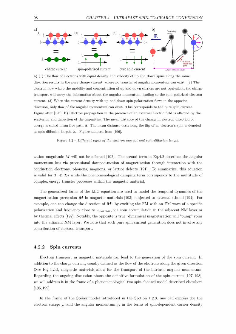
98 CHAPTER 4. ULTRAFAST SPIN-TO-CHARGE CONVERSION
a) (1) The flow of electrons with equal density and velocity of up and down spins along the samedirection results in the pure charge current, where no transfer of angular momentum can exist. (2) Theelectron flow where the mobility and concentration of up and down carriers are not equivalent, the chargetransport will carry the information about the angular momentum, leading to the spin-polarized electroncurrent. (3) When the current density with up and down spin polarization flows in the oppositedirection, only flow of the angular momentum can exist. This corresponds to the pure spin current.Figure after [195]. b) Electron propagation in the presence of an external electric field is affected by thescattering and deflection of the impurities. The mean distance of the change in electron direction orenergy is called mean free path Λ. The mean distance describing the flip of an electron’s spin is denotedas spin diffusion length, λs. Figure adapted from [196].
Figure 4.2 – Different types of the electron current and spin-diffusion length.
zation magnitude M will not be affected [192]. The second term in Eq.4.2 describes the angularmomentum loss via precessional damped-motion of magnetization through interaction with theconduction electrons, phonons, magnons, or lattice defects [191]. To summarize, this equationis valid for T ≪ TC while the phenomenological damping term corresponds to the multitude ofcomplex energy transfer processes within the magnetic material.
The generalized forms of the LLG equation are used to model the temporal dynamics of themagnetization precession M in magnetic materials [193] subjected to external stimuli [194]. Forexample, one can change the direction of M : by exciting the FM with an EM wave of a specificpolarization and frequency close to ωLarmor, via spin accumulation in the adjacent NM layer orby thermal effects [192]. Notably, the opposite is true: dynamical magnetization will "pump" spinsinto the adjacent NM layer. We note that such pure spin current generation does not involve anycontribution of electron transport.
4.2.2 Spin currents
Electron transport in magnetic materials can lead to the generation of the spin current. Inaddition to the charge current, usually defined as the flow of the electrons along the given direction(See Fig.4.2a), magnetic materials allow for the transport of the intrinsic angular momentum.Regarding the ongoing discussion about the definitive formulation of the spin-current [197, 198],we will address it in the frame of a phenomenological two spin-channel model described elsewhere[195,199].
In the frame of the Stoner model introduced in the Section 1.2.3, one can express the theelectron charge jc and the angular momentum js in the terms of spin-dependent carrier density
99 CHAPTER 4. ULTRAFAST SPIN-TO-CHARGE CONVERSION
ρ↑,↓ and velocity v↑,↓ as:
jc = j↑ + j↓ = −e(ρ↑v↑ + ρ↓v↓);
js = −ℏ2 (ρ↑v↑ − ρ↓v↓) = − ℏ
2e (j↑ − j↓).(4.3)
This equation summarizes three possible variations of the electron current depicted in Fig.4.2.Usually, in NM conductors, the equal density of the spin-up and spin-down electrons at the Fermilevel renders js = 0, establishing the pure charge current flow. However, in the FM both ρ↑ = ρ↓
and v↑ = v↓ are true, allowing for simultaneous charge and spin-current flow called spin-polarizedcurrent (see Fig.4.2a2). However, when j↑ = −j↓, as displayed in Fig.4.2a3, only the transport ofthe electron spin can exist, denoted as pure spin current. Moreover, the generation of the purespin current is quite challenging task, sometimes requiring extreme experimental conditions anduse of specific magnetic materials [200].
In analogy with the electron mean path Λ, the collision and scattering events may alter theparticles’ spin direction. The mean distance that thermalized electrons can travel without changein their angular momentum, or without so-called "spin-flip"(as shown in Fig.4.2b), is called spindiffusion length λs [201]:
λs = 1√3vF
√τsτe, (4.4)
where τs is the spin-flip time or spin lifetime. λs is directly linked to the electron velocity at theFermi level vF and scattering time τe. This equation, however, does not take into account thedifferent spin-flip diffusion lengths for the majority and minority of spin-polarized carriers due tothe asymmetric scattering [201]. Most materials with strong SOI are known to have short λs in theorder of tens of nanometers. The spin-flip is known to occur via two competing mechanisms: Elliot-Yafet, [202] which dominates for centrosymmetric conductors, and D’yakonov-Perel’ [203], superiorwithin the 2D systems and semiconductors (GaP, ZnTe, GaAs) lacking space-inversion symmetry.Interestingly, the Elliot-Yafet mechanism predicts the spin-rotation during the collisions, while theD’yakonov-Perel model describes spin-flip in-between scattering events.
4.2.3 Field-driven spin transport effects in DC (quasi-static)
Hall and Anomalous Hall effects
E.H. Hall in 1879 [204] discovered the transverse deflection of the charged particles in metalssubjected to the presence of an external magnetic field Bext. One can explain this observation inthe means of the classical Lorentz force, which acts on moving charged particles with speed v:
F = −e(E + v × Bext). (4.5)
About two years after, Hall discovered the same effect in ferromagnetic materials, which is ofone order of magnitude stronger [205]. Newly discovered Anomalous Hall effect (AHE) was thencombined with the Hall effect by Pugh and Lippert [206] to describe the total Hall resistivity (ρtot
xy )

100 CHAPTER 4. ULTRAFAST SPIN-TO-CHARGE CONVERSION
a) The ordinary Hall effect. Lorentz force is acting on the driving current jc in the presence of theexternal field Bext, resulting in the transverse Hall current jHE
c . b) The extraordinary or Anomalous Halleffect. The jc flow will generate the transverse spin-polarized current in the magnetic material withnon-zero macroscopic magnetization M = 0 via the Anomalous Hall Effect. Figure adapted from [44].
Figure 4.3 – The geometry of the Hall and Anomalous Hall effects.
in terms of both Hall (ρHall) and AHE (ρAHE) contributions:
ρtotxy = ρHallBext,z + ρAHEMz. (4.6)
It was observed that in the absence of M , i.e., when working with NM conductor, ρxy is increasinglinearly with Bext, as expected from Eqs.4.5,4.6. However, for the FM Ni, the ρxy linearly increasesat low Bext [207], and then rapidly saturates due to the parallel alignment of all spins along thedirection of the applied magnetic field [208].
The AHE describes the charge to spin-polarized current conversion. In general, the total AHEconductivity tensor (σAH
xy ) can be expressed as the sum of the following contributions [208]:
1ρAHE
xy
= σAHExy = σAHE−int
xy + σAHE−sjxy + σAHE−skew
xy , (4.7)
where σAHE−intxy , σAHE−sj
xy and σAHE−skewxy are the intrinsic, side-jump and skew-scattering con-
tributions shown in Fig.4.4.
Intrinsic deflection: The intrinsic contribution to the AHE (σAHE−intxy ) depends on the band
structure of the perfect crystal [209]. The total velocity of a Bloch electron in the band n, withband momentum k in the real space, in the presence of the applied electric field E can be writtenas [208,210]:
∂⟨r⟩dt
= 1ℏ∂ϵn(k)∂k︸ ︷︷ ︸
normal velocity
− ℏk
∂t× bn(k)︸ ︷︷ ︸
anomalous velocity
, (4.8)
where the first term corresponds to the ordinary electron velocity in the band n at the energy levelϵn(k). The second term introduces the transverse (anomalous) electron velocity perpendicular toboth applied E and Berry phase-curvature bn(k). bn(k) strongly depends on the electron band

101 CHAPTER 4. ULTRAFAST SPIN-TO-CHARGE CONVERSION
a) Intrinsic deflection. Electrons gain anomalous velocity perpendicular to the direction of the externalelectric field E that heavily depends on the electron band structure. b) Side-jump scattering. Electronswith opposite spins are deflected in the opposite directions due to the scattering of an impurity. c)Skew-scattering. Asymmetric, spin-dependent electron deflection as a result of the electron or impuritySOI. Adapted from [208]
Figure 4.4 – Schema of Hall Effect contributions.
structure, and it is the gauge-invariant representation of Bloch wave function geometric properties.The anomalous contribution is similar to the classical Lorentz force (see Eq.4.5). Still, it originatesfrom the SOI where bn(k) acts as a magnetic field in the momentum space [210]. The intrinsiccontribution usually dominates the side-jump and skew-scattering in pure crystals with large SOIand does not require electron scattering [211].
Side-jump scattering: The side-jump contribution (σAHE−sjxy ) to AHE is the scattering
process where electron momentum and energy are not affected. The scattering of the electronwave packet from the impurity will lead to spin-dependent transverse displacement. The electronswith opposite spins will experience an equal shift in the opposite directions, as shown in Fig.4.4b.Interestingly, the numerical prediction of the σAH−sj
xy is highly challenging since it depends on theintricate details of the material disorder.
Skew-scattering: Skew-scattering alters the electron momentum after interaction with theimpurity. Its efficiency is proportional to the electron scattering time τe [208]. Skew-scatteringcan occur in the presence of a strong SOI, leading to the spin-dependent change in the electronmomentum, as shown in Fig.4.4. Additionally, the skew-scattering can happen in the absence ofSOI, when the electrons are subject to motion in the spin-orbit-coupled band structure. The lattercan be thought of as the impurity-analogy of the heavy-atoms Mott-scattering [211].
Spin Hall and Inverse Spin-Hall effects
The description of the Spin Hall effect (SHE) and Inverse Spin Hall Effect (ISHE) are directlyrelated to the physics of the AHE. SHE and ISHE effects describe the conversion of the conservedcharge quantity to the decaying and dephasing amount of spin [211]. This defines the SHE andISHE as charge-to-spin and spin-to-charge conversion mechanisms respectively, first predicted byDyakonov and Perel in 1971 [212]. Similarly to the AHE, the SHE conductivity tensor σSH
xy canbe expressed as the sum of three mechanisms:
σSHxy = σSH−int
xy + σSH−sjxy + σSH−skew
xy , (4.9)
with σSH−intxy , σSH−sj
xy and σSH−skewxy being the intrinsic, side-jump and skew-scattering contribu-
tions, already discussed in the previous subsection.

102 CHAPTER 4. ULTRAFAST SPIN-TO-CHARGE CONVERSION
a) Spin Hall Effect. In the non-magnetic material (NM), the charge current flow will establish thetransverse spin current, due to the effective spin-orbit field experienced by the charged particles, inanalogy with Lorentz force. b) Inverse Spin Hall Effect. The pure spin current injected in the NM willresult in the transverse charge current due to the SOI. The figure is redrawn from [44,195]
Figure 4.5 – The geometry of the Spin Hall and Inverse Spin Hall effects.
The vital distinction between the AHE and the SHE is that AHE can happen only in mag-netic materials, while the SHE and the ISHE are suitable for all materials with strong SOI. Forexample, injection of pure spin current in the NM will establish transverse charge current due tothe asymmetric scattering arising from different concentration of the minority and majority spinpopulations at the Fermi level. Inversely, NM will convert pure spin current into pure chargecurrent.
The amount of spin or charge generated via the SHE and ISHE can be described with thefollowing equations [211]:
jSHEs = − ℏ
2eθSHE [jc × σs],
jISHEc = −2e
ℏθSHE [js × σs],
(4.10)
where θSHE is the so-called spin Hall angle that describes the conversion efficiency, and σs is theunit vector of the spin-/spin-current polarization.
The well-studied field-driven effects, such as AHE, SHE, and ISHE, are routinely used tomeasure and characterize spin currents. The magnitude of the θSHE can be measured by studyingthe efficiency of the spin-to-charge conversion with a variety of different techniques: FMR spin-pumping [213], thermal spin injection via the spin Seebeck effect [214], spin Hall magneto-resistance[215], and spin torque FMR [216].
Rashba-Edelstein and Inverse Rashba-Edelstein effects
As discussed in the Section 1.2.3, the Zeeman Hamiltonian can lift the spin degeneracy ofthe electronic band structure, leading to the Dresselhaus and Rashba splitting. However, specialconditions have to be fulfilled regarding the time-reversal and space-inversion symmetries of thematerial.
Symmetry considerations: When the time-reversal symmetry is preserved, i.e., T : t → −t,following the Kramer’s degeneracy theorem, the energies of fermions with opposite momentum
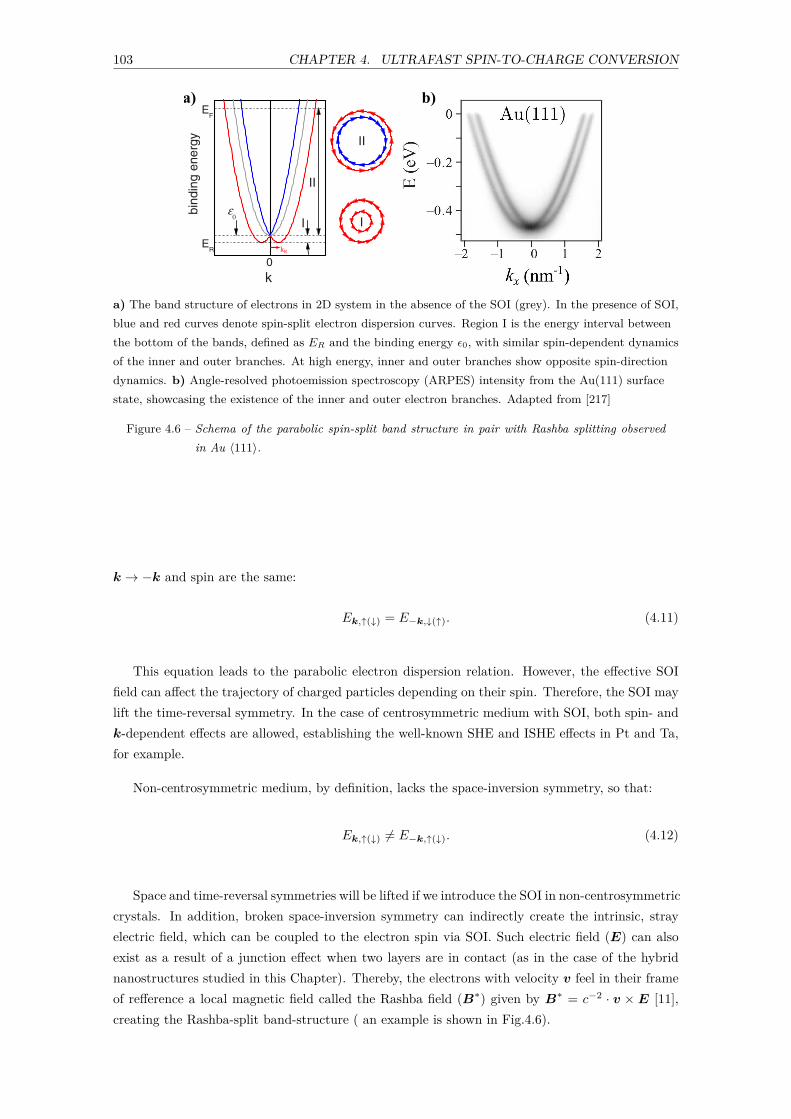
103 CHAPTER 4. ULTRAFAST SPIN-TO-CHARGE CONVERSION
a) The band structure of electrons in 2D system in the absence of the SOI (grey). In the presence of SOI,blue and red curves denote spin-split electron dispersion curves. Region I is the energy interval betweenthe bottom of the bands, defined as ER and the binding energy ϵ0, with similar spin-dependent dynamicsof the inner and outer branches. At high energy, inner and outer branches show opposite spin-directiondynamics. b) Angle-resolved photoemission spectroscopy (ARPES) intensity from the Au(111) surfacestate, showcasing the existence of the inner and outer electron branches. Adapted from [217]
Figure 4.6 – Schema of the parabolic spin-split band structure in pair with Rashba splitting observedin Au ⟨111⟩.
k → −k and spin are the same:
Ek,↑(↓) = E−k,↓(↑). (4.11)
This equation leads to the parabolic electron dispersion relation. However, the effective SOIfield can affect the trajectory of charged particles depending on their spin. Therefore, the SOI maylift the time-reversal symmetry. In the case of centrosymmetric medium with SOI, both spin- andk-dependent effects are allowed, establishing the well-known SHE and ISHE effects in Pt and Ta,for example.
Non-centrosymmetric medium, by definition, lacks the space-inversion symmetry, so that:
Ek,↑(↓) = E−k,↑(↓). (4.12)
Space and time-reversal symmetries will be lifted if we introduce the SOI in non-centrosymmetriccrystals. In addition, broken space-inversion symmetry can indirectly create the intrinsic, strayelectric field, which can be coupled to the electron spin via SOI. Such electric field (E) can alsoexist as a result of a junction effect when two layers are in contact (as in the case of the hybridnanostructures studied in this Chapter). Thereby, the electrons with velocity v feel in their frameof refference a local magnetic field called the Rashba field (B∗) given by B∗ = c−2 · v × E [11],creating the Rashba-split band-structure ( an example is shown in Fig.4.6).

104 CHAPTER 4. ULTRAFAST SPIN-TO-CHARGE CONVERSION
The Rashba Hamiltonian can be expressed as the interaction between the spin-vector s andthe electron momentum vector k as [184]:
HR ∝ B∗ × s = αR(k × z) · s, (4.13)
with the coordinate normal to the interface z, and the Rashba coefficient αR that is proportionalto the splitting-electric field. The Rashba Hamiltonian HR will lead to the following electrondispersion relation [4]:
E↑,↓(k) = ε0 + ℏ2k2
2m∗e
± |αR||k|, (4.14)
where ε0 is the band-crossing energy at k = 0 (see Fig.4.6a). Importantly, αR is not a constant,and can be expressed as:
αR = 2ER
kR, (4.15)
with ER being the band-splitting energy at k = kR [4], displaying the relationship between theRashba coefficient and the electron momentum.
The Rashba-split band structure allows for the charge-to-spin and spin-to-charge conversion. Itwas first theoretically predicted in 2D systems [218] and was later called Edelstein or spin-galvaniceffect [187]. The spin-galvanic effect was then first measured at the Ag/Bi interface [219].
Rashba Edelstein Effect: Let us consider the direct Rashba Edelstein effect (REE). Theaction of an external electric field Ex leads to a shift of the Fermi sphere. As a consequence thereis a total non-zero electron momentum in the x-direction with ∆kx ∝ −Ex ∝ −jx
c , as shown inFig.4.7a. The net spin current density generated under the action of Ex can be expressed as:
δs = δs↑ − δs↓ ∝ koutF δkx − kin
F δkx, (4.16)
where koutF and kin
F are the radii of the outer and inner Fermi contours. Considering similar electronscattering times for both contours, the finite spin accumulation will happen under the action ofEx or the injection of the charge current jx
c .
Inverse Rashba Edelstein Effect: Like the ISHE, the Inverse Rashba Edelstein effect(IREE) describes the charge current generation upon injection of the spin current at the Rashbainterface. As shown in Fig.4.7b, the injection of the spin-current polarized along the y-direction willshift the outer and inner Fermi contours by an equal amount δkx. However, the total displacementδktotal
x will be proportional to:
δktotalx ∝ ∆kout
x − ∆kinx ∝ kout
F δkx − kinF δkx. (4.17)
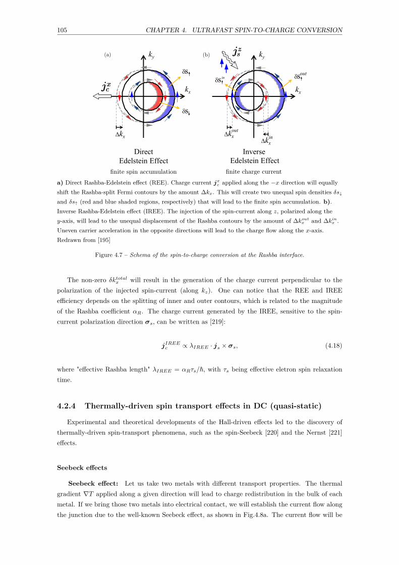
105 CHAPTER 4. ULTRAFAST SPIN-TO-CHARGE CONVERSION
a) Direct Rashba-Edelstein effect (REE). Charge current jxc applied along the −x direction will equally
shift the Rashba-split Fermi contours by the amount ∆kx. This will create two unequal spin densities δs↓
and δs↑ (red and blue shaded regions, respectively) that will lead to the finite spin accumulation. b).Inverse Rashba-Edelstein effect (IREE). The injection of the spin-current along z, polarized along they-axis, will lead to the unequal displacement of the Rashba contours by the amount of ∆kout
x and ∆kinx .
Uneven carrier acceleration in the opposite directions will lead to the charge flow along the x-axis.Redrawn from [195]
Figure 4.7 – Schema of the spin-to-charge conversion at the Rashba interface.
The non-zero δktotalx will result in the generation of the charge current perpendicular to the
polarization of the injected spin-current (along kz). One can notice that the REE and IREEefficiency depends on the splitting of inner and outer contours, which is related to the magnitudeof the Rashba coefficient αR. The charge current generated by the IREE, sensitive to the spin-current polarization direction σs, can be written as [219]:
jIREEc ∝ λIREE · js × σs, (4.18)
where "effective Rashba length" λIREE = αRτs/ℏ, with τs being effective eletron spin relaxationtime.
4.2.4 Thermally-driven spin transport effects in DC (quasi-static)
Experimental and theoretical developments of the Hall-driven effects led to the discovery ofthermally-driven spin-transport phenomena, such as the spin-Seebeck [220] and the Nernst [221]effects.
Seebeck effects
Seebeck effect: Let us take two metals with different transport properties. The thermalgradient ∇T applied along a given direction will lead to charge redistribution in the bulk of eachmetal. If we bring those two metals into electrical contact, we will establish the current flow alongthe junction due to the well-known Seebeck effect, as shown in Fig.4.8a. The current flow will be

106 CHAPTER 4. ULTRAFAST SPIN-TO-CHARGE CONVERSION
a) Seebeck effect. Temperature gradient ∇T applied to the two metals in contact, with differenttransport properties and Seebeck coefficients K1,2, will lead to the charge flow along the junction∝ ∇T (K1 −K2). b) Spin-dependent Seebeck effect. The different mobility of the majority and theminority electrons in the magnetic metal will result in the different spin-dependent Seebeck coefficientsSmaj and Smin respectively. The temperature gradient applied to the metal with the net magnetizationwill lead to the generation of the spin-polarized current ∝ ∇T (Smaj − Smin). c) Spin-Seebeck effect. Themagnons excited by the temperature gradient ∇T will carry the pure spin current along the direction ofthe gradient. Dominant in the magnetic insulators. From [44].
Figure 4.8 – Schemes of the multiple Seebeck effects.
proportional to:
jSEc ∝ ∇T (K1 −K2), (4.19)
where K1 and K2 are the Seebeck coefficients. The Seebeck effect is the operational principle ofthe thermocouples with K = ∆V/∆T the Seebeck constant and V is the Seebeck voltage.
Spin-dependent Seebeck Effect: The spin-dependent Seebeck effect (SDSE) describesthe generation of spin-polarized charge current (jSDSE
s−c ) under heat gradient ∇T in the bulkof a FM metal, shown in Fig.4.8. It is explained by the different transport properties of theminority- and majority-spin electrons that are related to the spin-dependent Seebeck coefficientsSmaj and Smin [222]:
jSDSEs−c ∝ ∇T (Smaj − Smin). (4.20)
However, the spin-diffusion length λs is the determining factor concerning the efficiency of theSDSE in the FM metals. The strong spin-flip scattering in the bulk of the FM layer can drasticallyreduce the number of spins injected in the neighboring NM layers [214,223].
Spin Seebeck Effect: Contrary to the SDSE, the spin Seebeck effect (SSE) is relatedto the generation of pure spin current (jSSE
s ) in magnetic insulators [220]. Here, the magnonscarry the pure spin current, which is usually detected by the ISHE in a NM layer. As shownin Fig.4.8c, this spin-current in the NM material is generated through the temperature differencebetween the electron temperature Te in the NM metal and magnon temperature TM in the magneticinsulator [224]:
jSSEs = KSSE · (Te − Tm), (4.21)
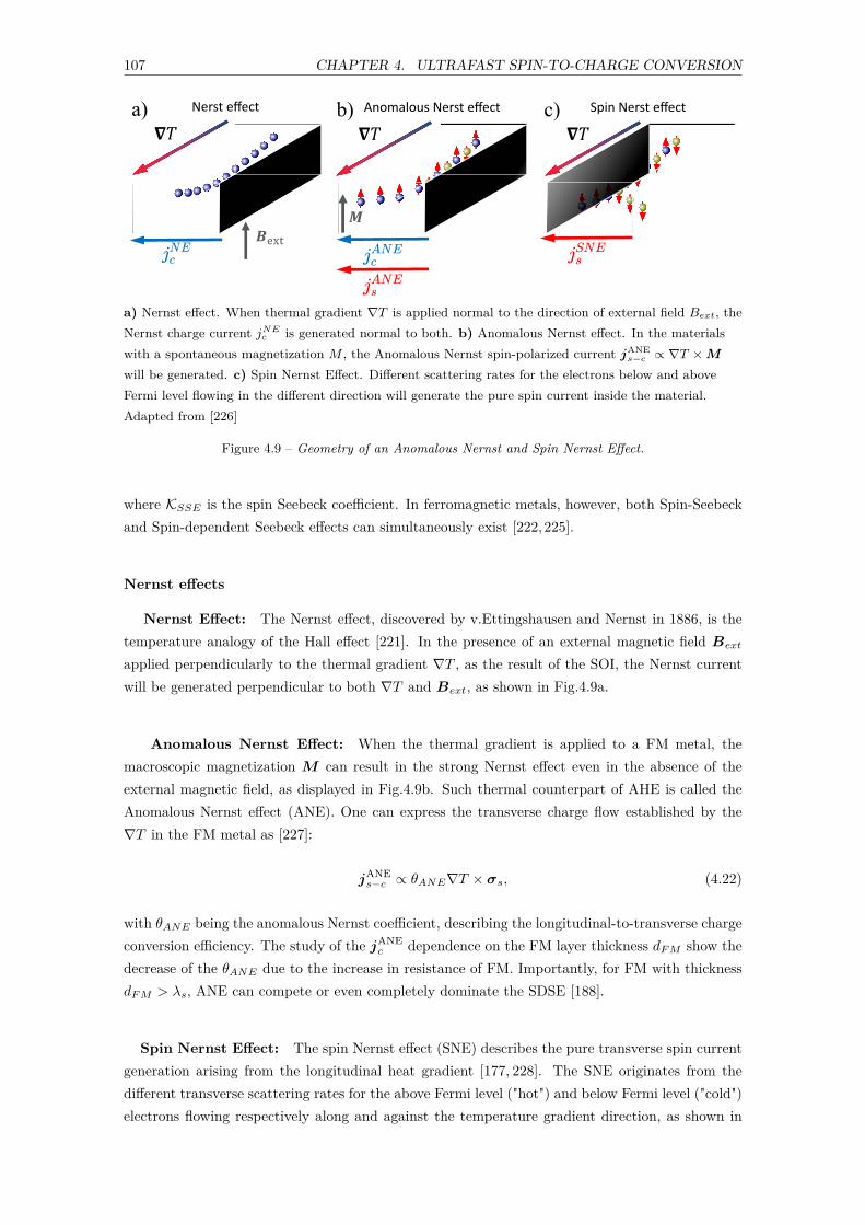
107 CHAPTER 4. ULTRAFAST SPIN-TO-CHARGE CONVERSION
a) Nernst effect. When thermal gradient ∇T is applied normal to the direction of external field Bext, theNernst charge current jNE
c is generated normal to both. b) Anomalous Nernst effect. In the materialswith a spontaneous magnetization M , the Anomalous Nernst spin-polarized current jANE
s−c ∝ ∇T × M
will be generated. c) Spin Nernst Effect. Different scattering rates for the electrons below and aboveFermi level flowing in the different direction will generate the pure spin current inside the material.Adapted from [226]
Figure 4.9 – Geometry of an Anomalous Nernst and Spin Nernst Effect.
where KSSE is the spin Seebeck coefficient. In ferromagnetic metals, however, both Spin-Seebeckand Spin-dependent Seebeck effects can simultaneously exist [222,225].
Nernst effects
Nernst Effect: The Nernst effect, discovered by v.Ettingshausen and Nernst in 1886, is thetemperature analogy of the Hall effect [221]. In the presence of an external magnetic field Bext
applied perpendicularly to the thermal gradient ∇T , as the result of the SOI, the Nernst currentwill be generated perpendicular to both ∇T and Bext, as shown in Fig.4.9a.
Anomalous Nernst Effect: When the thermal gradient is applied to a FM metal, themacroscopic magnetization M can result in the strong Nernst effect even in the absence of theexternal magnetic field, as displayed in Fig.4.9b. Such thermal counterpart of AHE is called theAnomalous Nernst effect (ANE). One can express the transverse charge flow established by the∇T in the FM metal as [227]:
jANEs−c ∝ θANE∇T × σs, (4.22)
with θANE being the anomalous Nernst coefficient, describing the longitudinal-to-transverse chargeconversion efficiency. The study of the jANE
c dependence on the FM layer thickness dF M show thedecrease of the θANE due to the increase in resistance of FM. Importantly, for FM with thicknessdF M > λs, ANE can compete or even completely dominate the SDSE [188].
Spin Nernst Effect: The spin Nernst effect (SNE) describes the pure transverse spin currentgeneration arising from the longitudinal heat gradient [177, 228]. The SNE originates from thedifferent transverse scattering rates for the above Fermi level ("hot") and below Fermi level ("cold")electrons flowing respectively along and against the temperature gradient direction, as shown in

108 CHAPTER 4. ULTRAFAST SPIN-TO-CHARGE CONVERSION
Fig.4.9c. Thus, spin current originating from the SNE can be expressed in terms of [229]:
jSNEs ∝ jHot
s − jColds ∝ θSNEjh × σs, (4.23)
where θSNE is the Spin Nernst coefficient and jh = −κ∇T is the heat current with κ being thethermal conductivity. The spin Nernst effect was directly observed in the heavy metal (HM) likeTungsten [230] or Platinum [177,229].
4.2.5 Terahertz emission as the signature of the ultrafast spin-chargeconversion
As of today, researchers are mainly focused on the characterization of the spin-to-charge con-version in the DC and GHz regimes via SHE and ISHE [211], AHE [208], SSE and SDSE [220,231],ANE [226], and IREE [184,232]. Hypothetically, all of these mechanisms can lead to the spin-chargeconversion not only at the GHz and DC frequencies but in the THz range as well.
The charge current generated from the spin-to-charge and charge-to-charge conversion withinthe FM/NM heterostructures is usually detected in the DC/GHz regime by placing physical con-tacts on top of the NM layer, used to measure the transverse current. On the other hand, inthe THz regime the spin-to-charge conversion can be probed in a non-contact manner [3, 233]. Ifwe recall the Maxwell wave-equation (see Eq.1.93), the transient charge current (jc) generated inthe heterostructure can act as the source term, responsible for the emission of an electromagneticradiation:
ETHz(t) ∝ ∂jc(t)∂t
. (4.24)
Let us consider what happens upon the excitation of the FM film by a femtosecond laser pulsepropagating along the z-axis. By applying the external magnetic field H along the x-axis to fixthe magnetization direction M of the FM layer (i.e. Hx ∥ Mx ∥ σx
s ), the total transverse spin-polarized current (jy
s,c) generated by the fs of laser pulse propagation inside the FM will be givenas:
jys,c(t) ∝
∑i
σxs (t) × jz
c,s(t), (4.25)
and it could be the combination of all possible spin-to-charge conversion mechanisms (such as AHE,ISHE, and IREE, DMG), as displayed in the Fig.4.10. As of today, for THz spintronic emitters, theISHE remains the most efficient conversion mechanism to date, completely overpowering ultrafastAHE and IREE conversion mechanisms [234,235]. The following section will provide a brief litera-ture overview of the most relevant and impactful studies about the THz spin-charge conversion inmagnetic nanometric heterostructures and ultrafast spin-injection mechanisms at the picosecondtimescale.
Supperdiffusive spin current injection
The ultrafast quenching of the magnetization in the ferromagnets at the 100 fs time scale wasaddressed with the superdiffusive spin transport theoretical model that relies on the spin-dependent
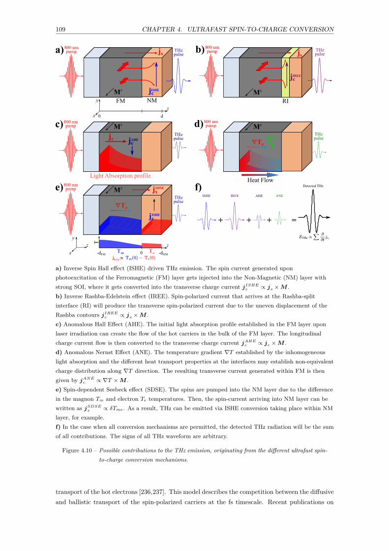
109 CHAPTER 4. ULTRAFAST SPIN-TO-CHARGE CONVERSION
a) Inverse Spin Hall effect (ISHE) driven THz emission. The spin current generated uponphotoexcitation of the Ferromagnetic (FM) layer gets injected into the Non-Magnetic (NM) layer withstrong SOI, where it gets converted into the transverse charge current jISHE
c ∝ js × M .b) Inverse Rashba-Edelstein effect (IREE). Spin-polarized current that arrives at the Rashba-splitinterface (RI) will produce the transverse spin-polarized current due to the uneven displacement of theRashba contours jIREE
c ∝ js × M .c) Anomalous Hall Effect (AHE). The initial light absorption profile established in the FM layer uponlaser irradiation can create the flow of the hot carriers in the bulk of the FM layer. The longitudinalcharge current flow is then converted to the transverse charge current jAHE
c ∝ jc × M .d) Anomalous Nernst Effect (ANE). The temperature gradient ∇T established by the inhomogeneouslight absorption and the different heat transport properties at the interfaces may establish non-equivalentcharge distribution along ∇T direction. The resulting transverse current generated within FM is thengiven by jANE
c ∝ ∇T × M .e) Spin-dependent Seebeck effect (SDSE). The spins are pumped into the NM layer due to the differencein the magnon Tm and electron Te temperatures. Then, the spin-current arriving into NM layer can bewritten as jSDSE
s ∝ δTme. As a result, THz can be emitted via ISHE conversion taking place within NMlayer, for example.f) In the case when all conversion mechanisms are permitted, the detected THz radiation will be the sumof all contributions. The signs of all THz waveform are arbitrary.
Figure 4.10 – Possible contributions to the THz emission, originating from the different ultrafast spin-to-charge conversion mechanisms.
transport of the hot electrons [236,237]. This model describes the competition between the diffusiveand ballistic transport of the spin-polarized carriers at the fs timescale. Recent publications on
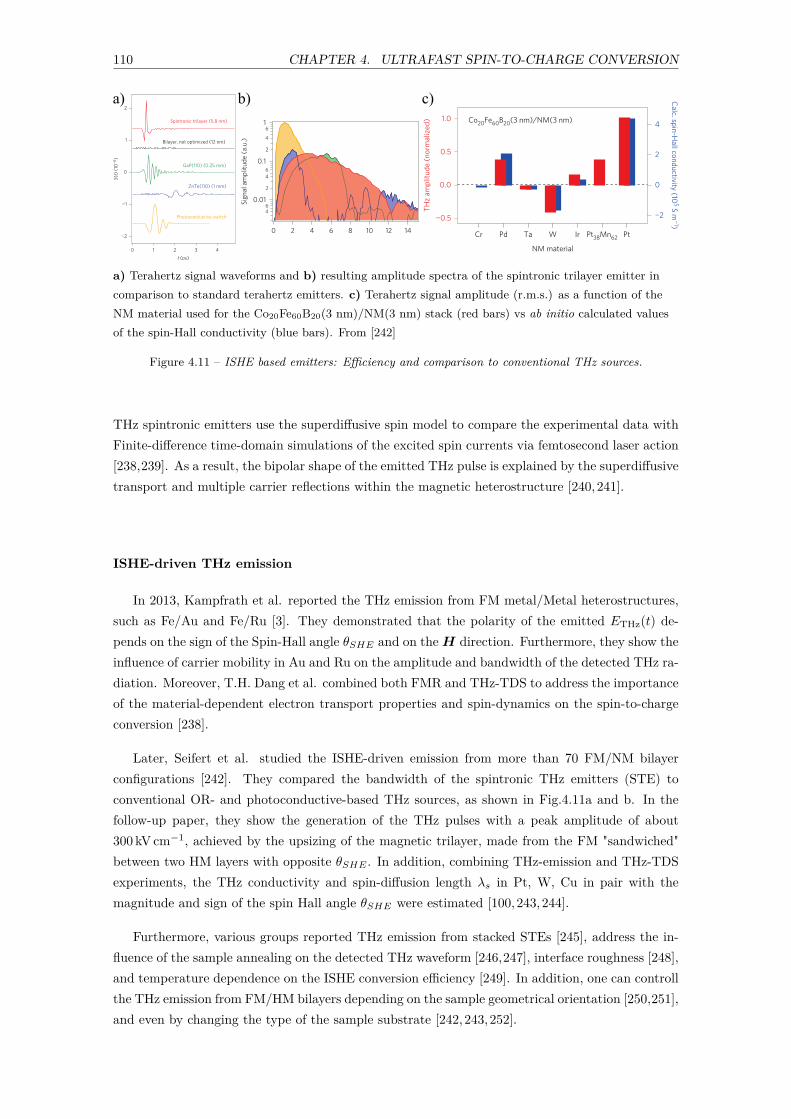
110 CHAPTER 4. ULTRAFAST SPIN-TO-CHARGE CONVERSION
a) Terahertz signal waveforms and b) resulting amplitude spectra of the spintronic trilayer emitter incomparison to standard terahertz emitters. c) Terahertz signal amplitude (r.m.s.) as a function of theNM material used for the Co20Fe60B20(3 nm)/NM(3 nm) stack (red bars) vs ab initio calculated valuesof the spin-Hall conductivity (blue bars). From [242]
Figure 4.11 – ISHE based emitters: Efficiency and comparison to conventional THz sources.
THz spintronic emitters use the superdiffusive spin model to compare the experimental data withFinite-difference time-domain simulations of the excited spin currents via femtosecond laser action[238,239]. As a result, the bipolar shape of the emitted THz pulse is explained by the superdiffusivetransport and multiple carrier reflections within the magnetic heterostructure [240,241].
ISHE-driven THz emission
In 2013, Kampfrath et al. reported the THz emission from FM metal/Metal heterostructures,such as Fe/Au and Fe/Ru [3]. They demonstrated that the polarity of the emitted ETHz(t) de-pends on the sign of the Spin-Hall angle θSHE and on the H direction. Furthermore, they show theinfluence of carrier mobility in Au and Ru on the amplitude and bandwidth of the detected THz ra-diation. Moreover, T.H. Dang et al. combined both FMR and THz-TDS to address the importanceof the material-dependent electron transport properties and spin-dynamics on the spin-to-chargeconversion [238].
Later, Seifert et al. studied the ISHE-driven emission from more than 70 FM/NM bilayerconfigurations [242]. They compared the bandwidth of the spintronic THz emitters (STE) toconventional OR- and photoconductive-based THz sources, as shown in Fig.4.11a and b. In thefollow-up paper, they show the generation of the THz pulses with a peak amplitude of about300 kV cm−1, achieved by the upsizing of the magnetic trilayer, made from the FM "sandwiched"between two HM layers with opposite θSHE . In addition, combining THz-emission and THz-TDSexperiments, the THz conductivity and spin-diffusion length λs in Pt, W, Cu in pair with themagnitude and sign of the spin Hall angle θSHE were estimated [100,243,244].
Furthermore, various groups reported THz emission from stacked STEs [245], address the in-fluence of the sample annealing on the detected THz waveform [246,247], interface roughness [248],and temperature dependence on the ISHE conversion efficiency [249]. In addition, one can controllthe THz emission from FM/HM bilayers depending on the sample geometrical orientation [250,251],and even by changing the type of the sample substrate [242,243,252].
111 CHAPTER 4. ULTRAFAST SPIN-TO-CHARGE CONVERSION
Ultrafast SSE spin current injection
Seifert et al. reported the injection of ultrafast spin current from the FM insulator into HMvia the SSE [253]. They note that the spin current injection is mediated by the thermal non-equilibrium between the electron and magnon baths in HM and FM insulators, respectively. Thebandwidth of the THz-SSE was then attributed to the electron-phonon coupling speed, the fewhundreds of femtoseconds after the laser excitation.
AHE-driven THz emission
Zhang et al. report that the THz emission can occur via AHE in the FM films with a thick-ness of less than 20 nm [235, 254]. In total, they measure the THz emission from four differentFM/MgO(4 nm) bilayers on the Quartz substrate. They claim that the charge gradient estab-lished within the FM is governed by the back-flow charge current, created by non-equal hot-carrierreflectance at the interfaces:
jc ∝ θAHE [r1 − r2], (4.26)
where r1 and r2 are the different hot-electron reflection coefficients at the Substrate/FM andFM/NM interfaces, respectively. For the case when r1 = r2, in the thin FM layer with homogeneouslight-absorption profile, the change in the geometrical orientation of the sample should lead to theTHz polarity reversal. Their model explains the THz polarity flip when STE is excited from theside of the substrate or MgO layer but does not explain the absence of the sign-reversal in thethick samples. In addition, they performed an experiment where they vary the Pt concentrationalong with the FM layer, which resulted in the amplification of the THz emission or even to thereversal of the polarity of the emitted THz.
The two-current model proposed by Zhang et.al. does not include the effect of the substrate(Quartz) and the capping layer (MgO) on the Pt distribution in the FM layer, which may leadto the accumulation of Pt with a higher concentration close to the given interface or affect thedistance between the scattering centers [255, 256]. Such interface-sensitive Pt buffer may amplifythe charge current generation, and introduce the sample asymmetry, which could explain the THzpolarity reversal in the thin samples observed by the authors [235]. In addition, they do not addressthe possible existence of the Rashba interface created at the FM/insulator interface [4, 257].
IREE-mediated THz emission
As of today, there are couple of papers speaking of an ultrafast spin-to-charge conversion viathe IREE at the Ag/Bi interface [234,258]. The authors demonstrate the importance of the Ag/Bistacking order and discuss the possible contribution of ISHE in Bi. Both works stress that theymeasure the superposition of the THz emitted via IREE and ISHE. However, the reported efficiencyof the THz emission with the IREE is about 50 times smaller than the one achieved with Pt-basedISHE emitters.
Importantly, for the Ag/Bi interface where the IREE leads to the THz emission, the phaseof the emitted THz pulse depends on the Ag/Bi layer ordering, which should be equivalent tochanging of the sample geometrical orientation [258]. As seen from Fig.4.12, the detected THzpulse is the sum or difference of the IREE contributions occurring at the Ag/Bi interface and
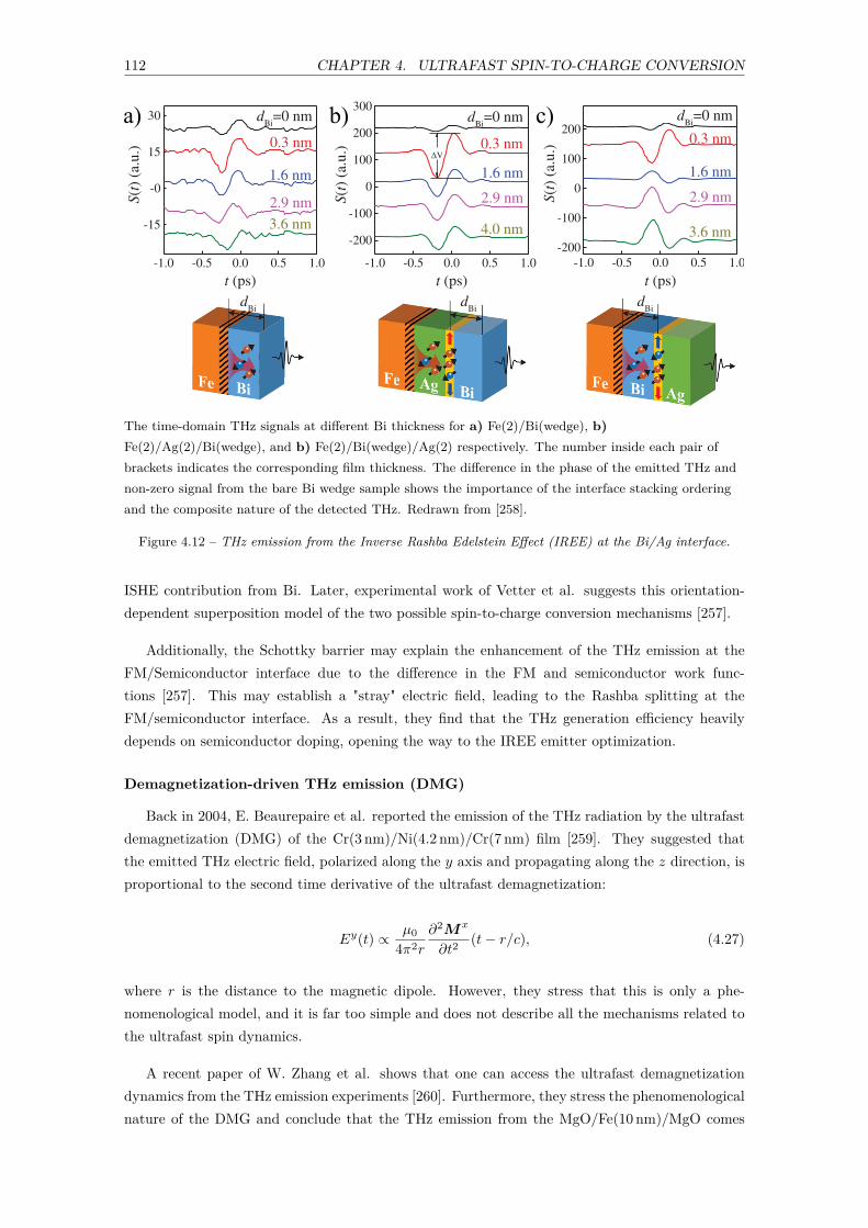
112 CHAPTER 4. ULTRAFAST SPIN-TO-CHARGE CONVERSION
The time-domain THz signals at different Bi thickness for a) Fe(2)/Bi(wedge), b)Fe(2)/Ag(2)/Bi(wedge), and b) Fe(2)/Bi(wedge)/Ag(2) respectively. The number inside each pair ofbrackets indicates the corresponding film thickness. The difference in the phase of the emitted THz andnon-zero signal from the bare Bi wedge sample shows the importance of the interface stacking orderingand the composite nature of the detected THz. Redrawn from [258].
Figure 4.12 – THz emission from the Inverse Rashba Edelstein Effect (IREE) at the Bi/Ag interface.
ISHE contribution from Bi. Later, experimental work of Vetter et al. suggests this orientation-dependent superposition model of the two possible spin-to-charge conversion mechanisms [257].
Additionally, the Schottky barrier may explain the enhancement of the THz emission at theFM/Semiconductor interface due to the difference in the FM and semiconductor work func-tions [257]. This may establish a "stray" electric field, leading to the Rashba splitting at theFM/semiconductor interface. As a result, they find that the THz generation efficiency heavilydepends on semiconductor doping, opening the way to the IREE emitter optimization.
Demagnetization-driven THz emission (DMG)
Back in 2004, E. Beaurepaire et al. reported the emission of the THz radiation by the ultrafastdemagnetization (DMG) of the Cr(3 nm)/Ni(4.2 nm)/Cr(7 nm) film [259]. They suggested thatthe emitted THz electric field, polarized along the y axis and propagating along the z direction, isproportional to the second time derivative of the ultrafast demagnetization:
Ey(t) ∝ µ0
4π2r
∂2Mx
∂t2(t− r/c), (4.27)
where r is the distance to the magnetic dipole. However, they stress that this is only a phe-nomenological model, and it is far too simple and does not describe all the mechanisms related tothe ultrafast spin dynamics.
A recent paper of W. Zhang et al. shows that one can access the ultrafast demagnetizationdynamics from the THz emission experiments [260]. Furthermore, they stress the phenomenologicalnature of the DMG and conclude that the THz emission from the MgO/Fe(10 nm)/MgO comes

113 CHAPTER 4. ULTRAFAST SPIN-TO-CHARGE CONVERSION
from ultrafast demagnetization in Fe. Importantly, they say that THz emission from single-layerferromagnet could have a contribution of the coherent-phonon driven magneto-elastic effect.
From this brief literature overview, we see that there are many reports on different spin-to-charge (SCC) mechanisms at the ultrafast timescale. Therefore, the dominant mechanism of theSCC may vary depending on the sample orientation, the choice of FM metal/insulator and/orthe capping layer. As a result, it might not be so straightforward to address and study the SCCconversion mechanism of interest. Therefore, in the next section, we will to propose a way how toexperimentally identify the different contributions to the ultrafast SCC in CoFeB/MgO magneticbilayers. At the end, we will compare the THz emission from the CoFeB/MgO samples andconventional CoFeB/Pt STEs.
4.3 Experimental results
Sample choice: In this section, we measure the THz emission from the MgO-based spin-tronic emitters and compare the results to the well-known CoFeB/Pt samples. Here, we areinterested in the efficiencies of the injection-based IREE (CoFeB/MgO), ISHE (CoFeB/Pt), andbulk (CoFeB) SCC mechanisms at the sub-picosecond timescales. Furthermore, we will try toidentify the different driving mechanisms of the SCC based on the sample experimental geometry,pump-fluence dependence, and the influence of the pump wavelength on the THz emission. Con-sequently, we discuss THz emission from four different STEs: CoFeB(5)/Pt(3), CoFeB(20)/Pt(3),CoFeB(5)/MgO(6) and CoFeB(20)/MgO(6) on the SiO2 and Si substrates, where number in theparentheses is the thickness of the preceding layer in nm.
We chose the CoFeB layer with an equivalence ratio of Co40/Fe40/B20 due to the highestreported efficiency of the THz emission [242] in pair with already measured THz conductivity[100].The capping layers, namely 3 nm of Pt and 6 nm of MgO were grown on top of the CoFeB inthe same sputtering chamber. Pt layer was chosen as the "reference" since it is the most efficientspin-to-charge converting HM, and it is well characterized both in DC and at the picosecondtimescale. As mentioned in the introduction, the deposition of MgO on top of the CoFeB layercreates the Rashba states inside the FM metal close to CoFeB/MgO interface [4]. All the sampleswere grown at the Condensed Matter Physics laboratory of IRAMIS (Saclay Institute for Radiationand Matter) by J.B. Moussy, A. Solignac, J.Y. Chauleau, and M Viret.
Experimental details: The experiments were performed with the 1 kHz 165 fs amplified laser,operating at the central wavelength of 800 nm. The output laser beam was split 90/10, where 90%of the laser power was used to pump the STE, while the remaining 10% used for electroopticdetection.
STE with the size of 0.5 mm × 0.5 mm was fixed in the sample holder with a hole of ≈ 0.45 mmin diameter. Unfocused pump beam with the ≈ 0.48 mm beam diameter at FWHM was incidentnormal to the surface of the STE. The THz pulse, emitted along with the pump direction, wasseparated with the combination of two two-millimeter thick HDPE sheets followed by the half-millimeter thick silicon wafer. The THz beam was then focused with one-inch gold, unprotectedoff-axis parabolic mirror (OAPM) with a six-inch focal length. The lateral position of the samplerelative to the OAPM remained fixed through the experiment. The emitted THz was recorded with

114 CHAPTER 4. ULTRAFAST SPIN-TO-CHARGE CONVERSION
a) Experimental configuration, where the pump beam is incident from the side of the SiO2 substrate. b)Detected THz signals, for the + (solid line) and − (dotted line) direction of the applied externalmagnetic field H, where the number in parentheses corresponds to the thickness in nm of the precedinglayer. c) THz polarization characterization setup. For a fixed direction of the external magnetic field HTHz power is measured as a function of the Wire-Grid polarizer (WG) angle. d) Experimental geometry,displaying two orthogonal orientations of H. e) CoFeB(5)/Pt(3): THz power measured for the Verticaland Horizontal orientation of external applied H, with the setup shown in c). The polarization of theemitted THz is always perpendicular to the direction of the applied direction of H. The same behavior isobserved for all samples.
Figure 4.13 – Pt and MgO samples: Terahertz emission - External Magnetic field dependence.
the EOS technique, discussed in the Section 2.4. The probe beam intensity was kept below thetwo-photon absorption limit of ZnTe, in pair with the constant optical power seen by the balancedphotodiodes. In our experiment, the direction of the external magnetic field H was controlledby the pair of magnets introduced into the rotating sample holder, to insure the homogeneousmagnetic field distribution across the sample. The applied magnetic field strength is in the orderof 0.2 T, enough to saturate the CoFeB magnetization.

115 CHAPTER 4. ULTRAFAST SPIN-TO-CHARGE CONVERSION
External magnetic field dependence and polarization of the emitted THzradiation
As the first experiment, we check the magnetic origin of the THz emission. For this, we installthe samples (CoFeB covered either with Pt or MgO) in the sample holder with the two magnets,such as the pump beam first hits the substrate, as shown in Fig.4.13a. The emitted THz was thenrecorded for two opposite orientations of the external magnetic field ±H, shown in Fig.4.13b (solidand dotted lines). Figure 4.13b shows that all samples are sensitive to the direction of H, and180° rotation of H in the xy-plane leads to the complete polarity reversal of the emitted THz.We should note the slight difference in the emitted THz amplitude (up to 5 %) between waveformsrecorded for ±H that can be attributed to the manual rotation of the magnets.
In addition, we have measured the polarization of the THz emitted from the CoFeB(5)/Pt(3)sample, using the pyroelectric detector and a Wire Grid (WG) polarizer, as shown in Fig.4.13c.For two orientations of the external magnetic field H (displayed in Fig.4.13d), we find that theTHz polarization is linear and perpendicular to the direction of the external magnetic field (seeFig.4.13e), in perfect agreement with previously published results [3]. Furthermore, the THzpolarization of the CoFeB(20)/Pt(3) and CoFeB(5 or 20)/MgO(6) bilayer is linear and follows thesame tendency.
Sample geometry-dependent THz emission
Next, we study the THz emission from the CoFeB(Pt or MgO) heterostructures within twodifferent geometrical sample orientations: we define the Front Face sample orientation when thepump beam is incident from the side of the substrate, while the excitation from the nonmagneticlayer will be called the Back Face configuration, with the two displayed in Figure 4.14a. Forthe fixed laser pump fluence Φ, Figure 4.14b shows ETHz waveform, emitted in the Front Face(color) and Back Face (grey) experimental configurations. The Front Face signals were normalizedto the peak-to-peak amplitude of the CoFeB(5)/Pt(3) emitter (blue line), with a scaling factormentioned above respective signal in Fig.4.14b. First, we observe the additional temporal delayfor the THz emitted in the Back Face related to the emitted THz pulse propagation throughglass. In addition, the broadening of the THz waveform in the Back configuration occurs dueto the frequency-dependent glass THz absorption (see Section 2.4). The same effect was alreadyobserved before [243, 261, 262]. Nevertheless, we report THz polarity reversal as a function of thesample orientation (color vs. grey line) for all the samples presented in Figure 4.14b, except forthe CoFeB(20)/MgO(6).
To measure the undistorted THz waveform in the Back Face geometrical orientation, the sam-ples were grown on the high-resistivity, float-zone silicone (Si) substrate. The pump fluence wasthen adjusted to equalize the absorbed density of energy in the CoFeB layer to the Front Face exci-tation 1. All signals were normalized to the peak-to-peak amplitude of the CoFeB(5)/Pt(3) bilayerin the Front Face orientation. The Figure 4.14c shows a complete reversal of the CoFeB(5)/Pt(3)and CoFeB(20)/Pt(3) THz waveforms upon the sample flip around the y-axis. Such change in theTHz polarity upon the flip of the ISHE emitter has been reported numerous times [242,245,262,263].
1. Calculated with the Transfer Matrix Method. The light absorption profiles are shown in the Appendix C.
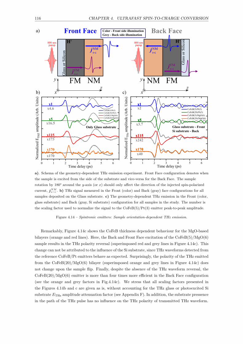
116 CHAPTER 4. ULTRAFAST SPIN-TO-CHARGE CONVERSION
a). Schema of the geometry-dependent THz emission experiment. Front Face configuration denotes whenthe sample is excited from the side of the substrate and vice-versa for the Back Face. The samplerotation by 180° around the y-axis (or x) should only affect the direction of the injected spin-polarizedcurrent, jNM
s−c . b) THz signal measured in the Front (color) and Back (gray) face configurations for allsamples deposited on the Glass substrate. c) The geometry-dependent THz emission in the Front (color,glass substrate) and Back (gray, Si substrate) configuration for all samples in the study. The number isthe scaling factor used to normalize the signal to the CoFeB(5)/Pt(3) emitter peak-to-peak amplitude.
Figure 4.14 – Spintronic emitters: Sample orientation-dependent THz emission.
Remarkably, Figure 4.14c shows the CoFeB thickness dependent behaviour for the MgO-basedbilayers (orange and red lines). Here, the Back and Front Face excitation of the CoFeB(5)/MgO(6)sample results in the THz polarity reversal (superimposed red and grey lines in Figure 4.14c). Thischange can not be attributed to the influence of the Si substrate, since THz waveforms detected fromthe reference CoFeB/Pt emitters behave as expected. Surprisingly, the polarity of the THz emittedfrom the CoFeB(20)/MgO(6) bilayer (superimposed orange and grey lines in Figure 4.14c) doesnot change upon the sample flip. Finally, despite the absence of the THz waveform reversal, theCoFeB(20)/MgO(6) emitter is more than four times more efficient in the Back Face configuration(see the orange and grey factors in Fig.4.14c). We stress that all scaling factors presented inthe Figures 4.14b and c are given as is, without accounting for the THz glass or photoexcited Sisubstrate ETHz amplitude attenuation factor (see Appendix F). In addition, the substrate pressencein the path of the THz pulse has no influence on the THz polarity of transmitted THz waveform.
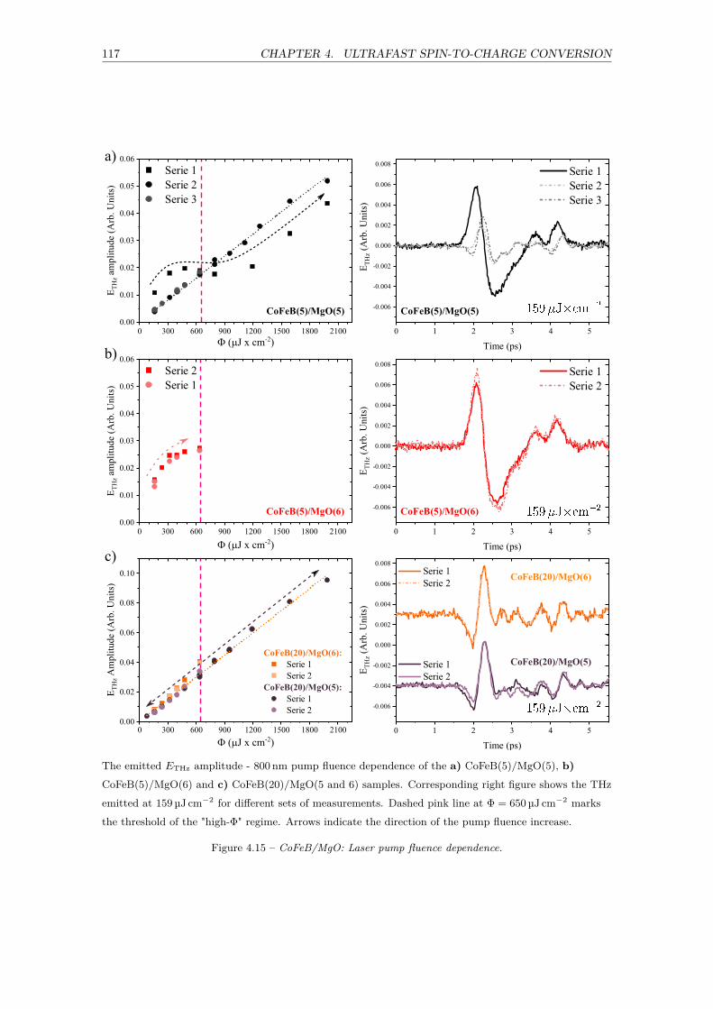
117 CHAPTER 4. ULTRAFAST SPIN-TO-CHARGE CONVERSION
The emitted ETHz amplitude - 800 nm pump fluence dependence of the a) CoFeB(5)/MgO(5), b)CoFeB(5)/MgO(6) and c) CoFeB(20)/MgO(5 and 6) samples. Corresponding right figure shows the THzemitted at 159 µJ cm−2 for different sets of measurements. Dashed pink line at Φ = 650 µJ cm−2 marksthe threshold of the "high-Φ" regime. Arrows indicate the direction of the pump fluence increase.
Figure 4.15 – CoFeB/MgO: Laser pump fluence dependence.
118 CHAPTER 4. ULTRAFAST SPIN-TO-CHARGE CONVERSION
CoFeB/MgO pump fluence dependence
In this subsection, we present the pump fluence dependence of the CoFeB/MgO samples, whenthe data for the CoFeB/Pt emitters is presented in the Appendix D. Here, we introduce the"control" samples CoFeB(5)/MgO(5) and CoFeB(20)/MgO(5), that were grown in the differentbatch and behave the same as their CoFeB/MgO(6) counterpart. The direction of the externalmagnetic field H and sample orientation (Front Face) was kept fixed through the experiment.
The first experiment was conducted for the "control" CoFeB(5)/MgO(5) bilayer grown on theglass substrate. All the experiments are performed as independent sets of measurements, denoted"Series". The Figure 4.15a shows that within Serie 1 measurement, the ETHz amplitude - laserpump fluence (Φ) dependence of CoFeB(5)/MgO(5) sample evolves in a highly nonlinear manner.In addition, from Figure 4.15a we see the presence of a turning point of ETHz-pump Φ dependenceat the Φcrit ≈ 650 µJ cm−2 (the dashed pink line). Surprisingly, the Serie 2 and Serie 3 mea-surements of CoFeB(5)/MgO(5) emitter show clear linear ETHz dependence as the function of Φ(see Fig.4.15a). In addition, the right panel of Fig.4.15a displays the complete change in the THzwaveform and polarity between the Series 1 and Series 2, while the shape of the detected ETHz
between Serie 2 and Serie 3 experiments remains unchanged. This indeed indicates that we havepermanently modified the CoFeB(5)/MgO(5) emitter after it was exposed to Φcrit. For the futurerefference, we will denote the "after Serie 1" state of this sample as CoFeB(5)/MgO(5)*.
As the next step, we measured laser pump fluence dependence for the CoFeB(5)/MgO(6) emit-ter, up to the pump laser fluence Φcrit ≈ 650 µJ cm−2. From Fig.4.15b, we report the nonlinearincrease in the ETHz amplitude as the function of Φ, already seen for the Serie 1 CoFeB(5)/MgO(5)sample measurement. The panels of Fig.4.15b shows that both ETHz-pump Φ dependence and THzwaveform of CoFeB(5)/MgO(6) measured within Serie 1 and Serie 2 experiment remains mostlyunchanged, which confirms the existence of the "threshold" effect above Φcrit.
The last ETHz amplitude-Φ dependence was measured for the CoFeB(20)/MgO(5) andCoFeB(20)/MgO(6) samples. Here, only the CoFeB(20)/MgO(5) bilayer was measured abovethe threshold Φcrit, while CoFeB(20)/MgO(6) was studied with Φ < 650 µJ cm−2 range. As wesee from the Figure 4.15c, both CoFeB(20)/MgO(5) and CoFeB(20)/MgO(6) samples show clearlinear ETHz amplitude-pump Φ dependence. In addition, the right panel of Figure 4.15c (darkviolet and light violet curves) shows no significant change in the polarity and the waveform ofCoFeB(20)/MgO(5), even after Φcrit exposure. The CoFeB(20)/MgO(6) emitter (solid and dash-dot lines in the left panel of Fig.4.15c) remains perfectly intact and unchanged between the Serie1 and Serie 2 experiments. Therefore, we conclude that CoFeB(20)-based samples seem not to beaffected by the high-laser fluence.
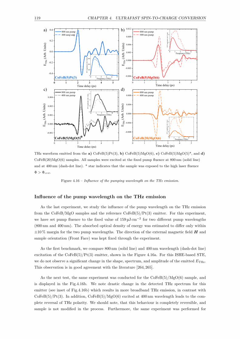
119 CHAPTER 4. ULTRAFAST SPIN-TO-CHARGE CONVERSION
THz waveform emitted from the a) CoFeB(5)Pt(3), b) CoFeB(5)MgO(6), c) CoFeB(5)MgO(5)*, and d)CoFeB(20)MgO(6) samples. All samples were excited at the fixed pump fluence at 800 nm (solid line)and at 400 nm (dash-dot line). * star indicates that the sample was exposed to the high laser fluenceΦ > Φcrit.
Figure 4.16 – Influence of the pumping wavelength on the THz emission.
Influence of the pump wavelength on the THz emission
As the last experiment, we study the influence of the pump wavelength on the THz emissionfrom the CoFeB/MgO samples and the reference CoFeB(5)/Pt(3) emitter. For this experiment,we have set pump fluence to the fixed value of 159 µJ cm−2 for two different pump wavelengths(800 nm and 400 nm). The absorbed optical density of energy was estimated to differ only within±10 % margin for the two pump wavelengths. The direction of the external magnetic field H andsample orientation (Front Face) was kept fixed through the experiment.
As the first benchmark, we compare 800 nm (solid line) and 400 nm wavelength (dash-dot line)excitation of the CoFeB(5)/Pt(3) emitter, shown in the Figure 4.16a. For this ISHE-based STE,we do not observe a significant change in the shape, spectrum, and amplitude of the emitted ETHz.This observation is in good agreement with the literature [264,265].
As the next test, the same experiment was conducted for the CoFeB(5)/MgO(6) sample, andis displayed in the Fig.4.16b. We note drastic change in the detected THz spectrum for thisemitter (see inset of Fig.4.16b) which results in more broadband THz emission, in contrast withCoFeB(5)/Pt(3). In addition, CoFeB(5)/MgO(6) excited at 400 nm wavelength leads to the com-plete reversal of THz polarity. We should note, that this behaviour is completely reversible, andsample is not modified in the process. Furthermore, the same experiment was performed for
120 CHAPTER 4. ULTRAFAST SPIN-TO-CHARGE CONVERSION
CoFeB(5)/MgO(5)* 2 and is shown in Figure 4.16c. Interestingly, CoFeB(5)/MgO(5)* does notseem to be affected by the change of the pump wavelength, similarly to CoFeB(5)/Pt(3).
Finally, the pump wavelength dependence measured for the CoFeB(20)/MgO(6) is shown inFig4.16d. Again, this sample behaves differently from the CoFeB(5)/MgO(6) bilayer. Figure4.16d demonstrates that CoFeB(20)/MgO(6) excited at 400 nm wavelength does not show themodification in the polarity and spectral components of emitted THz radiation, but results in thethree-fold increase of the ETHz amplitude.
4.4 Discussion
First off all, we will speak about the "prototypical" ISHE-based emitters, i.e., the conventionalCoFeB(5 and 20)/Pt(3) bilayers. We observe that the THz emission from CoFeB(5 and 20)/Pt(3)samples is affected by the external magnetic field orientation and is polarized perpendicular tothe direction of external magnetic field H (see Figs.4.13b and e). Next, Figures 4.14b and cdemonstrate the THz waveform polarity reversal when bilayer is excited from the side of thesubstrate (Front Face) or from the side of the Pt capping layer (Back Face). Finally, we findthat THz emission from CoFeB(5)/Pt(3) is not affected by the change of the pump wavelength, asseen from Figure 4.16a. All these observations are in perfect agreement with previously publishedresults [3, 242,264,265].
For the novel samples in this study, i.e., CoFeB/MgO bilayers, we find that the polarity of theemitted THz is sensitive and perpendicular to H (see Fig.4.13e), similarly to CoFeB/Pt emitters.However, for the geometry, pump fluence Φ, and pump wavelength measurements, the CoFeB/MgOemitters behave differently depending on the CoFeB thickness. For example, Figures 4.14b and cdemonstrate that THz polarity reversal between the Back and Front Face bilayer orientation wasobserved only for CoFeB(5)/MgO(6), while we report no change for CoFeB(20)/MgO(6) sample.In addition, the excitation of the CoFeB(5)/MgO(6) emitter at 400 nm, compared to 800 nm pumpwavelength leads to the THz polarity reversal and broadening of the THz spectrum (see 4.16b). Theexcitation of the CoFeB(20)/MgO(6) results in the three times more important ETHz amplitudes,as depicted in Fig.4.16d. No ETHz polarity/spectrum modification was observed for this sample.
At last, pump Φ dependence has revealed the highly nonlinear increase in the emitted THzfield amplitudes for the CoFeB(5)/MgO(6) bilayer (see Fig.4.15b), but clear linear dependencefor CoFeB(20)/MgO(6) (Fig.4.15c). Moreover, Figure 4.15a reveals that the power dependenceand ETHz waveform of the "control" CoFeB(5)/MgO(5) sample 3 could be altered when exposed topump fluence Φ > 650 µJ cm−2. In addition, the ETHz emitted from "modified" CoFeB(5)/MgO(5)sample is no longer sensitive to the change of the pump wavelength, as shown in the Figure 4.16c.
Based on the Section 4.2.5 discussion and Figure 4.10, multiple SCC mechanisms can contributeto the total detected ETHz, and can be split into two "categories": the one that originates from theSCC within the bulk of the FM metal (AHE and/or DMG, for example), and another emergingfrom the addition of the capping layer like Pt or MgO (ISHE and IREE, respectively). With thisin mind, for two separate systems (CoFeB/Pt and CoFeB/MgO) this concept of combined THz
2. Reminder: star means the sample state after high-Φ exposure.3. Which in its pristine condition was equivalent to CoFeB(5)/MgO(6).

121 CHAPTER 4. ULTRAFAST SPIN-TO-CHARGE CONVERSION
emission can be phenomenologically formulated as:
EtotTHz(CoFeB/MgO) = ξCoFeB · Ebulk
THz + βMgO · EIREETHz ,
EtotTHz(CoFeB/Pt) = ξCoFeB · Ebulk
THz + γPt · EISHETHz ;
(4.28)
where ξCoFeB , βMgO and γPt are the phenomenological coefficients describing the SCC efficiencyinside the bulk of the CoFeB (ξCoFeB), at the Rashba interface (βMgO), and due to the ISHE withinthe Pt layer (γPt). ξCoFeB is present in both CoFeB/Pt and CoFeB/MgO systems and can originatefrom DMG [259,266–268] and/or Anomalous Hall Effect (AHE) [44,269]. One should note that weneglect the possible existence of the Rashba interface at the CoFeB/Pt interface [239]. With thisphenomenological formulation, we will proceed with the discussion about the sample geometry,pump fluence Φ and wavelength dependence, in order to evaluate the relative bulk and IREEcontributions of CoFeB/MgO-based samples.
External magnetic field dependence: We now address why the direction of the externalmagnetic field H affects the polarization of the emitted THz radiation. Following the discussion ofSection 4.2 and Eq.4.25, the direction of the converted transverse charge current (jc) is defined asthe vector product between spin-polarized current flow (jz
c,s) and direction of the FM macroscopicmagnetization (M), defining the polarization of the spin current σs as:
jc(t) ∝∑
i
M(t) × jzc,s(t), (4.29)
where the sum over i represents all possible spin-to-charge (SCC) contributions to the transversetransient charge current jc(t). From the latter equation, we see that the direction of generated jc
should be sensitive and perpendicular to M . As the sample is subjected to an external magneticfield H, its macroscopic magnetization M will be aligned parallel to H. Therefore, from theEq.4.29 the polarization of the emitted ETHz via SCC must be sensitive to H direction. As shownin the Figure 4.13b, the rotation of the H by 180° leads to the 180° THz polarity reversal for bothCoFeB/Pt and CoFeB/MgO samples. This confirms the magnetic origin of the THz emission fromCoFeB/MgO bilayers.
The following discussion will be split into two parts: first, we address the difference in the THzemission behavior from CoFeB(5)/MgO(6) and CoFeB(20)/MgO(6) emitters in the low-fluenceregime, and in the second part we focus on the consequences of the permanent CoFeB(5)/MgO(5)sample modification.
Low-fluence regime (pristine samples):
This subsection deals only with the unchanged samples, i.e., that were not exposed to laserfluence above Φcrit ≈ 650 µJ cm−2.
Sample geometry dependence: As the first step, we address the possible origin of the THzpolarity reversal due to the different sample geometry. Since the IREE, as ISHE, is an injection-based SCC mechanism, the polarity of the emitted THz should depend on the jz
c,s direction inrespect to the Rashba interface. Consequently, the sample rotation around the y-axis will change

122 CHAPTER 4. ULTRAFAST SPIN-TO-CHARGE CONVERSION
the direction of jzc,s (jz
c,s → j−zc,s , see Fig.4.14a) and, according to Eq.4.29 it will lead to the polarity
reversal of the emitted THz field. This effect is well known for the ISHE-based emitters [242,270],and an identical experiment conducted by Vetter et al. [257] (Front and Back Face pumping) onthe n-GaN/NiFe bilayers IREE-based emitters. As seen from the Figure 4.14b and c, for theCoFeB(5)/MgO(6) STE we observe the complete ETHz polarity reversal between the Front Faceand Back Face sample orientations (see red and grey curves). Hence, as a first element of conclusion,we can attribute the observed THz polarity reversal in CoFeB(5)/MgO(6) to the presence of theinjection-based IREE SCC mechanism.
Now we discuss the symmetry of the bulk SCC contribution to the emitted THz. From the liter-ature, it is well known that the efficiency of the injection-based ISHE emitters scales inversely withthe FM layer thickness [245,246,251]. Moreover, for the Co films, Huang et al. demonstrated thatthe bulk SCC contribution increases with the FM layer thickness (i.e., ξCo(30 nm) > ξCo(5 nm)) to thepoint that the THz amplitudes detected from 30 nm Co are not affected by the deposition of the HMTantalum (ξCo(30 nm) > γTa) [268]. The combination of these reports indicates that with an increaseof the FM layer thickness, one should simultaneously increase the bulk contribution (ξCoFeB), whiledecreasing the injection-based SCC contribution (γP t and βMgO) to the total emitted Etot
THz. Thispeculiar effect is usually attributed to the short hot-electron spin diffusion length in the CoFeB (inthe order of couple of nm) [242, 251]. Since the THz emission from the bulk contribution (AHE,DMG, or combination of both) should be governed by the spin-polarized current flow inside theFM layer, its direction should not be altered upon the sample flip. As a result, the absence of theETHz polarity reversal between Back and Front Face configurations should be a strong indicationof the bulk-dominant SCC. Indeed, as shown in the Figure 4.14 (orange vs grey curves), we observethe absence of the ETHz polarity reversal between Back and Front Face configurations for the thickCoFeB(20)/MgO(6) sample. This means that the THz emission from CoFeB(20)/MgO(6) emitteris mainly governed by the bulk SCC (i.e. ξCoFeB(20) > βMgO). It is worth to note that this argu-ment does not hold when comparing CoFeB(5)/Pt(3) and CoFeB(20)/Pt(3) since ξCoFeB ≪ γPt,even for 20 nm thick CoFeB [251].
Laser pump fluence dependence: Let us now address the pump fluence Φ-ETHz ampli-tude dependence. From the CoFeB(5)/MgO(6) measurement, shown in Figure 4.15b, we see theclear nonlinear increase in the emitted THz field amplitudes as a function of Φ. This could beexplained by the competition of bulk ξCoFeB and IREE βMgO SCC mechanisms (see Eq.4.28) hav-ing opposite signs, and possibly different SCC pump fluence efficiencies. At the same time, forthe CoFeB(20)/MgO(6) emitter, we measure linear ETHz(Φ) dependence. Such linear behaviour,previously reported for the bare Co films [268] again confirms our suggestion that the THz emis-sion from CoFeB(20)/MgO(6) is dominated by the SCC in the bulk of the CoFeB layer (i.e.,ξCoFeB(20) > βMgO). We do not expect the nonlinear behaviour from the bulk contribution sincethe pump-fluence dependent magnitude of the ultrafast demagnetization in the thin ferromagneticlayers is known to be linear for the fluence below 4 mJ cm−2 [271–273]. Regardless, time-resolvedmagneto-optical measurements for the set of CoFeB bilayers are to be measured in the future.
Laser pump wavelength dependence: From the Figure 4.16a we see that the change of thepump wavelength from 800 nm to 400 nm has no effect on the ISHE-based CoFeB(5)/Pt(3) emitter,as expected from the literature [264, 265]. The pump wavelength-independent THz emission fromCoFeB(5)/Pt(3) can be attributed to the fact that spin-dependent electron deflection and scatter-
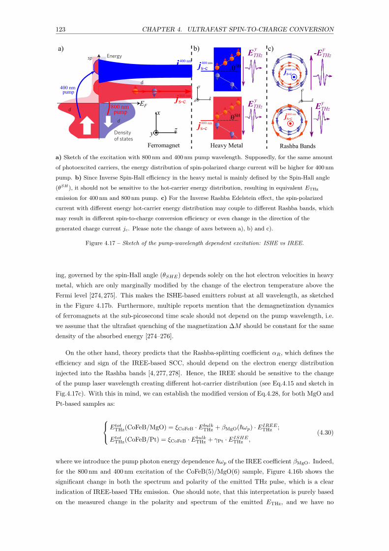
123 CHAPTER 4. ULTRAFAST SPIN-TO-CHARGE CONVERSION
a) Sketch of the excitation with 800 nm and 400 nm pump wavelength. Supposedly, for the same amountof photoexcited carriers, the energy distribution of spin-polarized charge current will be higher for 400 nmpump. b) Since Inverse Spin-Hall efficiency in the heavy metal is mainly defined by the Spin-Hall angle(θSH), it should not be sensitive to the hot-carrier energy distribution, resulting in equivalent ETHz
emission for 400 nm and 800 nm pump. c) For the Inverse Rashba Edelstein effect, the spin-polarizedcurrent with different energy hot-carrier energy distribution may couple to different Rashba bands, whichmay result in different spin-to-charge conversion efficiency or even change in the direction of thegenerated charge current jc. Please note the change of axes between a), b) and c).
Figure 4.17 – Sketch of the pump-wavelength dependent excitation: ISHE vs IREE.
ing, governed by the spin-Hall angle (θSHE) depends solely on the hot electron velocities in heavymetal, which are only marginally modified by the change of the electron temperature above theFermi level [274, 275]. This makes the ISHE-based emitters robust at all wavelength, as sketchedin the Figure 4.17b. Furthermore, multiple reports mention that the demagnetization dynamicsof ferromagnets at the sub-picosecond time scale should not depend on the pump wavelength, i.e.we assume that the ultrafast quenching of the magnetization ∆M should be constant for the samedensity of the absorbed energy [274–276].
On the other hand, theory predicts that the Rashba-splitting coefficient αR, which defines theefficiency and sign of the IREE-based SCC, should depend on the electron energy distributioninjected into the Rashba bands [4, 277, 278]. Hence, the IREE should be sensitive to the changeof the pump laser wavelength creating different hot-carrier distribution (see Eq.4.15 and sketch inFig.4.17c). With this in mind, we can establish the modified version of Eq.4.28, for both MgO andPt-based samples as:
EtotTHz(CoFeB/MgO) = ξCoFeB · Ebulk
THz + βMgO(ℏωp) · EIREETHz ;
EtotTHz(CoFeB/Pt) = ξCoFeB · Ebulk
THz + γPt · EISHETHz ,
(4.30)
where we introduce the pump photon energy dependence ℏωp of the IREE coefficient βMgO. Indeed,for the 800 nm and 400 nm excitation of the CoFeB(5)/MgO(6) sample, Figure 4.16b shows thesignificant change in both the spectrum and polarity of the emitted THz pulse, which is a clearindication of IREE-based THz emission. One should note, that this interpretation is purely basedon the measured change in the polarity and spectrum of the emitted ETHz, and we have no

124 CHAPTER 4. ULTRAFAST SPIN-TO-CHARGE CONVERSION
Figure 4.18 – Light absorption profiles: in the CoFeB(5)/MgO(6) and CoFeB(20)/MgO(6) bilayers, inFront Face configuration on the Glass substrate, for 800 and 400 nm pump wavelengths.
information about the electronic structure of the Rashba bands at the CoFeB/MgO interface.Moreover, multiple Rashba bands may simultaneously participate in the SCC, and laser lightabsorption may lead to electron-hole creation, furthermore modifying the ultrafast dynamics andefficiency of IREE-based THz emitter.
From the previous discussion, we concluded that the THz emission from CoFeB(20)/MgO(6)is mainly mediated by the bulk contribution (ξCoFeB(20) > βMgO). However, for the same amountof the absorbed density of energy Figure 4.16d demonstrates no change in the THz polarity, buta three-fold increase in the ETHz amplitude when the sample is excited at 400 nm compared to800 nm. We propose to explain this observation with the instantaneous hot-carrier flux/gradientinside the CoFeB, which should be important for the bulk spin-to-charge conversion, especially inthick single-layer FM films [259, 268]. Figure 4.18 shows the light absorption gradient calculatedfor both CoFeB(20)/MgO(6) (orange) and CoFeB(5)/MgO(6) (red) samples using the TransferMatrix method 4. The position 0 indicates the initial point of the laser impact. The average profileof the light absorption ∇Az was then estimated using the following equation:
∇Az = Aabs(0) −Aabs(d)d
, (4.31)
where Aabs(0) and Aabs(d) are the fractions of the absorbed optical power at the beginning (z = 0)and the end of the FM layer (z = d). Importantly, for the CoFeB(20)/MgO(6) bilayer, the absorbeddensity of energy between 400 nm and 800 nm differs only by less than 10 %, while the ∇Az hasincreased by the factor of 2.5. In this case, the three times increase in the ETHz observed for400 nm excitation (see Fig.4.16d) may be directly linked to the 2.5 times more important lightabsorption gradient (see Fig.4.18) in the CoFeB layer. Even though such explanation does notcontradict previous hypothesis of the bulk-dominant ultrafast SCC, it is yet to be confirmed withsingle-layer FM STEs with various thicknesses.
4. See Appendix C for more details.

125 CHAPTER 4. ULTRAFAST SPIN-TO-CHARGE CONVERSION
Left: Sketch of the injection-based IREE spin-to-charge conversion in the CoFeB/MgO emitters. Right:The relative amplitudes of the Inverse Rashba Edelstein (IREE) and bulk contributions to the THzemission from the CoFeB/MgO bilayers, estimated with Eq.4.32. Factors are the ratios between thepeak-to-peak values of ETHz emitted from CoFeB(5)/Pt(3) and given contribution.
Figure 4.19 – Sketch of the relative amplitudes of the IREE and bulk contributions to the emitted THzfrom CoFeB/MgO bilayers.
Estimate of the bulk and IREE contributions: As the final step, we will make an attemptto evaluate the relative amplitudes of the IREE and bulk contributions to SCC from CoFeB/MgOemitters. To do so, we start with an estimate of the decrease in injection-based (ISHE, IREE) SCCrelated to the increase of the CoFeB thickness. From Fig.4.14b and c, we see that for the constantthickness of the Pt layer, the THz emission from the CoFeB(20)/Pt(3) bilayer is reduced by thefactor of five when compared to CoFeB(5)/Pt(3) emitter (blue vs. green ratios). Such decrease inthe total emitted THz can be attributed to the short spin-diffusion length in CoFeB [242,251] andpossible Fabry–Pérot cavity effect, that may enhance the THz emission due to the multiple pumpand THz reflections at the CoFeB/Pt and substrate/CoFeB interfaces [242]. In this case, sinceγPt ≫ ξCoFeB, we can assign this five-fold decrease in THz emission to the reduced amount of thespin current injected in the HM Pt layer and diminished Fabry–Pérot for the thick CoFeB(20)/Pt(3)sample [251].
We then can use this factor to estimate the relative amplitudes of competing bulk and IREEcontributions inside the CoFeB/MgO bilayers. Since the IREE-based conversion happens close tothe CoFeB/MgO interface [4], we can assume the same five-fold decrease in IREE contributionfor the CoFeB(20)/MgO(6) as was observed in CoFeB(20)/Pt(3). However, for the CoFeB/MgOemitters we cannot neglect bulk contribution so we have to account for the change in the lightgradient absorption ∇Az between CoFeB(20)/MgO(6) and CoFeB(5)/MgO(6) bilayers. From Fig-ure 4.18a, for 800 nm pump wavelength we have calculated the factor of 0.37/0.08 = 4.625, whichreflects non-equal gradient of the light absorption in 5 and 20 nm of CoFeB. This 4.625 factorshould correspond to the increase in the bulk contribution of CoFeB(20)/MgO(6) compared toCoFeB(5)/MgO(6), meaning ξCoFeB(20) ≈ 4.625 · ξCoFeB(5). With this, the observed difference inthe emitted THz amplitudes and polarities (see red and orange ratios from the Figure 4.14c) canbe used to write the following linear system of equations (with arbitrary units, i.e., one can extract
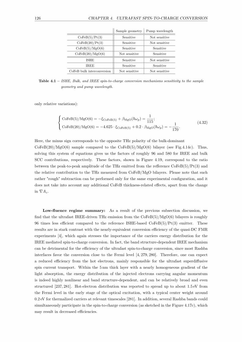
126 CHAPTER 4. ULTRAFAST SPIN-TO-CHARGE CONVERSION
Sample geometry Pump wavelength
CoFeB(5)/Pt(3) Sensitive Not sensitiveCoFeB(20)/Pt(3) Sensitive Not sensitive
CoFeB(5)/MgO(6) Sensitive SensitiveCoFeB(20)/MgO(6) Not sensitive Sensitive
ISHE Sensitive Not sensitiveIREE Sensitive Sensitive
CoFeB bulk interconversion Not sensitive Not sensitive
Table 4.1 – ISHE, Bulk, and IREE spin-to-charge conversion mechanisms sensitivity to the samplegeometry and pump wavelength.
only relative variations):
CoFeB(5)/MgO(6) = −ξCoFeB(5) + βMgO(ℏωp) = 1115 ;
CoFeB(20)/MgO(6) = −4.625 · ξCoFeB(5) + 0.2 · βMgO(ℏωp) = − 1170 .
(4.32)
Here, the minus sign corresponds to the opposite THz polarity of the bulk-dominantCoFeB(20)/MgO(6) sample compared to the CoFeB(5)/MgO(6) bilayer (see Fig.4.14c). Thus,solving this system of equations gives us the factors of roughly 96 and 580 for IREE and bulkSCC contributions, respectively. These factors, shown in Figure 4.19, correspond to the ratiobetween the peak-to-peak amplitude of the THz emitted from the refference CoFeB(5)/Pt(3) andthe relative contribution to the THz measured from CoFeB/MgO bilayers. Please note that suchrather "rough" subtraction can be performed only for the same experimental configuration, and itdoes not take into account any additional CoFeB thickness-related effects, apart from the changein ∇Az.
Low-fluence regime summary: As a result of the previous subsection discussion, wefind that the ultrafast IREE-driven THz emission from the CoFeB(5)/MgO(6) bilayers is roughly96 times less efficient compared to the reference ISHE-based CoFeB(5)/Pt(3) emitter. Theseresults are in stark contrast with the nearly-equivalent conversion efficiency of the quasi-DC FMRexperiments [4], which again stresses the importance of the carriers energy distribution for theIREE mediated spin-to-charge conversion. In fact, the band structure-dependent IREE mechanismcan be detrimental for the efficiency of the ultrafast spin-to-charge conversion, since most Rashbainterfaces favor the conversion close to the Fermi level [4, 279, 280]. Therefore, one can expecta reduced efficiency from the hot electrons, mainly responsible for the ultrafast superdiffusivespin current transport. Within the 5 nm thick layer with a nearly homogeneous gradient of thelight absorption, the energy distribution of the injected electrons carrying angular momentumis indeed highly nonlinear and band structure-dependent, and can be relatively broad and evenstructured [237, 281]. Hot-electron distribution was reported to spread up to about 1.5 eV fromthe Fermi level in the early stage of the optical excitation, with a typical center weight around0.2 eV for thermalized carriers at relevant timescales [281]. In addition, several Rashba bands couldsimultaneously participate in the spin-to-charge conversion (as sketched in the Figure 4.17c), whichmay result in decreased efficiencies.
127 CHAPTER 4. ULTRAFAST SPIN-TO-CHARGE CONVERSION
To conclude this part of the discussion, we present the Table 4.1, where we compare the sensitiv-ity of the ISHE, bulk, and IREE conversion mechanisms on the sample geometrical orientation andpump wavelength. Therefore, we deduce that the THz emission from CoFeB(5)/MgO(6) bilayer ismainly mediated by the IREE mechanism. In contrast, the THz generation in CoFeB(20)/MgO(6)emitter mainly occurs via spin-charge conversion in the bulk of the CoFeB layer, and wavelengthsensitivity is explained by more important FM light absorption gradient at 400 nm. The addi-tional data on the CoFeB/Pt samples and power-dependence measurement for CoFeB/Pt andCoFeB/MgO on the Si substrate are presented in Appendix D and Appendix F, respectively.
High-fluence regime:
In this last subsection, we demonstrate that the delicate Rashba-split bands in CoFeB(5)/MgO(5)emitter could be modified or even destroyed at high laser fluence, leading to bulk-like THz emis-sion. Here, we address the modification of the "test" CoFeB(5)/MgO(5) sample, when exposedto Φ > 650 µJ cm−2. As shown in Figure 4.15a, the pristine (Serie 1) CoFeB(5)/MgO(5) bi-layer emits a similar waveform and has nonlinear pump-fluence dependence in Φ < 650 µJ cm−2
range, just as CoFeB(5)/MgO(6). However, when the CoFeB(5)/MgO(5) sample was exposed toΦ > 650 µJ cm−2, we observed the "threshold" effect, which resulted in a drastic change in bothTHz waveform and ETHz(Φ) dependence (see Figs 4.15a, Serie 2 and Serie 3). Furthermore, themeasured linear ETHz(Φ) dependence for Serie 2 and Serie 3 measurements (see Fig.4.15a) suggeststhe irreversible sample modification.
We now compare the ETHz waveform emitted from CoFeB(5)/MgO(5) (black solid) andCoFeB(5)/MgO(5)* (black dash-dot), shown in the Figure 4.15a. For the convenience, the samedata is displayed in the Figure 4.20b, and complemented with THz transients recorded for theBack and Front Face sample geometrical orientations. From the Figure 4.20b we see that the THzemission from CoFeB(5)/MgO(5)* bilayer is somewhat symmetric, as in the case of bulk-dominantCoFeB(20)/MgO(6) emitter. Moreover, as shown in the Figure 4.16c, CoFeB(5)/MgO(5)* sample800 nm or 400 nm wavelength excitation shows no significant effect on the EThz amplitude andspectrum. This, compared to the reference ISHE-based emitter (CoFeB(5)/Pt(3), see Fig.4.16a)and bulk-dominant STE (CoFeB(20)/MgO(6), Fig.4.16d), strongly suggests the "disappearance"of the Rashba states, with preserved bulk contribution, such as ξCoFeB(5) ≫ βMgO. Since thisirreversible modification happened to the same sample, we could re-write the Eq.4.28 as.
EtotTHz(CoFeB(5)/MgO(5)) = ξCoFeB(5) · Ebulk
THz + βMgO · EIREETHz ;
EtotTHz(CoFeB(5)/MgO(5)*) = ξCoFeB(5)* · Ebulk
THz .(4.33)
Of course, the latter equation is valid under the assumption that Rashba bands do not affect theSCC within the CoFeB layer, i.e. ξCoFeB(5)* = ξCoFeB(5). In this case, the difference between theTHz transients emitted by the CoFeB(5)/MgO(5) and CoFeB(5)/MgO(5)* should give us onlythe IREE contribution, shown as the red line in Figure 4.20c. For the CoFeB(5)/MgO(5) bilayer,we estimate the 1:2.75 ratio between the bulk and IREE contribution. This is a relatively goodagreement with the estimation of IREE-to-bulk ratio of 1:6 made at the end of the low-fluencesection. The factor of two difference between the low-fluence and high-fluence regime is most likelyrelated to the fact that we used CoFeB/Pt to approximate the decrease in IREE contribution

128 CHAPTER 4. ULTRAFAST SPIN-TO-CHARGE CONVERSION
a). Schema of the geometry-dependent THz emission experiment. Front Face configuration denotes whenthe sample is excited from the side of the substrate and vice-versa for the Back Face. jIREE
s−c is thespin-polarized current directed towards the Rashba interface. b) THz signal emitted from pristineCoFeB(5)/MgO(5) (solid) and CoFeB(5)/MgO(5)* (dash-dot) in the Front (color) and Back (gray) faceconfigurations at 159 µJ cm−2 fluence and 800 nm pump wavelength. Temporal delay and waveformbroadening for the Back Face orientation are due to the frequency-dependent THz absorption in the glasssubstrate. c) Extracted IREE contribution (red), obtained as the difference between the Front-Facesignal, measured before and after sample modification. Bulk contribution is the CoFeB(5)/MgO(5)*waveform. The scaling factors indicate the ratio between the reference CoFeB(5)/Pt(3) emitter and thegiven signal. d) Normalized to 1 Fast Fourier transform of the c).
Figure 4.20 – CoFeB(5)/MgO(5): Sample orientation-dependent THz emission.
for the CoFeB(20)/MgO(6) sample. Of course, at this moment, we can completely rely on thelatter guesstimate of the relative amplitudes of IREE and bulk contributions using the permanent"modification" of the CoFeB(5)/MgO(5)* bilayer, since the absence of the Rashba states in theCoFeB(5)/MgO(5)* needs to be confirmed with ARPES or XPS measurements, if possible.
4.5 Conclusions and perspectives
In this chapter, we have discussed the THz emission as a result of the ultrafast spin-to-charge conversion from CoFeB/Pt and CoFeB/MgO magnetic bilayers. While CoFeB/Pt sampleswere chosen as the most characterized and best-performing bilayers to date, the choice of theCoFeB/MgO structures was stimulated by the recent discovery of the Rashba states created bythe deposition of insulating MgO nanofilm on top of the ferromagnetic CoFeB layer. We show thatby analyzing the effect of the sample geometrical orientation, laser pump fluence and wavelengthdependence on the polarity and the shape of the emitted THz, one can identify the dominant spin-
129 CHAPTER 4. ULTRAFAST SPIN-TO-CHARGE CONVERSION
to-charge conversion mechanism. On the first hand, we find that our measurements of CoFeB/Ptemitters are in the perfect agreement with the literature. On the other hand, we observed thestrong thickness dependence of THz emission from the CoFeB/MgO bilayers, which we attributeto the combination of the spin-to-charge conversion in the bulk of the CoFeB ferromagnet and atthe CoFeB/MgO Rashba interface. For the CoFeB(20 nm)/MgO(6 nm) sample, it appears that thebulk contribution is the dominant spin-to-charge conversion mechanism. In particular, we reportthat the sample reversal does not affect the polarity of the emitted THz, as expected from thespin-to-charge conversion inside the bulk of CoFeB layer. This claim is supported by the linearETHz amplitude - pump fluence dependence, previously reported for the thick single-layer ferro-magnetic films [268]. In contrast, in the CoFeB(5)/MgO(6) emitter we find that Inverse RashbaEdelstein effect contributes the most to the total detected ETHz, despite the presence of the bulkspin-to-charge conversion. This conclusion is supported by the sample-geometry dependent THzemission characteristic to the injection-based THz emitters, and highly-nonlinear emitted THzfield amplitude - pump fluence dependence that indicates the competition of the bulk and Rashbacontributions.
Consequently, we have estimated the 1:6 ratio between the amplitudes of the emitted THzfields driven by the bulk and Inverse Rashba Edelstein conversion in CoFeB(5)/MgO(6) emitter.This estimation makes the ultrafast Inverse Rashba Edelstein conversion in CoFeB(5)/MgO(6)nearly 100 less efficient than the Inverse Spin Hall effect in CoFeB(5)/Pt(3). At the same time,the Inverse Spin Hall and Inverse Rashba Edelstein effects are found to be equivalently efficientfor the thermalized spin-polarized carriers [4]. Such difference in the Inverse Rashba Edelsteinand Inverse spin Hall conversion rates at the ultrafast and quasi-DC timescales may indicate thereduced Rashba conversion efficiency when dealing with non-thermal distribution of injected spin-polarized carriers, since most Rashba bands favor spin-to-charge conversion close to the Fermilevel [4, 279, 280]. Moreover, we evidenced pump wavelength sensitivity of the Inverse-RashbaEdelstein CoFeB/MgO emitters. While for CoFeB(20)/MgO(6) bilayer such change might beattributed to the more important light absorption gradient inside the CoFeB layer, the differencein THz emission (polarity of the emitted THz field, spectrum) observed for CoFeB(5)/MgO(6)sample is directly related to the spin-to-charge conversion at the Rashba interface. To the best ofour knowledge, this finding was never mentioned in the literature before. Finally, we show that atthe high laser pump fluence (higher than 650 µJ cm−2) one may permanently modify or damagethe delicate Rashba interface, which leads to the purely bulk spin-to-charge conversion.
As the future prospects, one can imagine tuning the Rashba bands to favor the conversion athigh carrier-energies. This may result in a highly efficient, wavelength-sensitive spintronic device,allowing for an easy tunability of the generated THz waveform amplitude and spectrum. In ad-dition, the estimation of the electrooptic response function, which includes the spatio-temporaltransformation of the emitted THz pulse may allow us to access the shape of the transient chargecurrent generated in the bulk of the CoFeB and at the Rashba interface. This information, comple-mented with a future in-lab time-resolved magneto-optical Kerr effect setup will certainly facilitatethe first-principle calculations, anticipated in the near future.

130 CHAPTER 4. ULTRAFAST SPIN-TO-CHARGE CONVERSION

General conclusion
In this thesis, we study how terahertz (THz) radiation could be used to excite or probe theultrafast dynamics of electron, phonon, and spin in solids and nanostructures. In particular, weaddress the generation of coherent phonons in metals such as Chromium (Cr) and Aluminum (Al)and narrow-band topological insulator Bismuth Telluride (Bi2Te3) with picosecond THz pulses.In addition, we demonstrate how the specific aspects of the THz emission from optically-excitedCoFeB/Pt and CoFeB/MgO magnetic nanostructures may provide insights into the relevant ultra-fast spin-to-charge interconversion mechanisms.
The experiments in this manuscript were done using the ultrafast nonlinear spectroscopy inthe pump-probe geometry with 1 kHz 800 nm 3 mJ amplified laser. For the ultrafast excitation ofCr, Al, and Bi2Te3 films, we have used the tilted-pulse front method for Lithium Niobate crystal(LiNbO3) to generate the THz pulses with a peak electric field of about 275 kV cm−1 with a centralfrequency of 0.64 THz, that corresponds to a 1.2 µJ pulse energy. In the experimental section, weshow how birefringent x−cut Quartz crystal could be used to shape the THz pulse, we calculatethe electro-optic response function for the GaP and ZnTe electro-optic crystals and discuss thetechnique of THz time-domain spectroscopy sensitivity enhancement used for the detection of theweak THz fields in the Chapter 4.
As a first achievement of this thesis, we show that one can generate coherent phonons withpulsed THz radiation in the thin films of metals and narrow-band semiconductors. First, wediscussed the THz excitation of 14 nm thick Cr and 20 nm thick Al films, and compared it towell-known 800 nm pump excitation. We find that the general shape of the time-dependent changein the 400 nm probe beam transmittance is similar for the THz and near-IR (NIR) excitation. Wedetect the thin metallic film first harmonic acoustic breathing mode for the NIR and THz pumpexcitation. Finally, comparing the electron (deformation potential) and lattice (thermoelastic)contributions to the total photoinduced stress for both types of excitation allowed us to identifythermoelastic stress as the main driving mechanism of acoustic phonon generation with THz. Weconclude that the lattice heating is linked to the scattering of the accelerated electrons at the Fermilevel, which leads to an ultrafast analogy of the well-known Joule effect.
The second achievement of this work is the investigation of the coherent optical phonon gener-ation in Bi2Te3 16 nm thin film with THz. We demonstrate that 1.3 ps THz pulse with the centralfrequency of 0.64 THz is able to excite symmetric A1
1g 1.85 THz Raman active phonon. We showthat the A1
1g phonon amplitude increases quadratically with the THz field amplitude, indicatingthe second-order nonlinear process required to excite such coherent motion. We find as well that
131
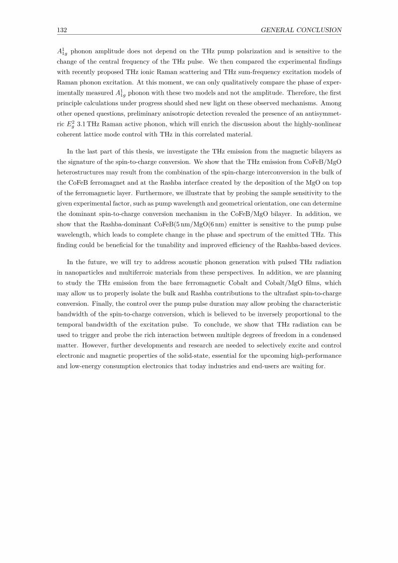
132 GENERAL CONCLUSION
A11g phonon amplitude does not depend on the THz pump polarization and is sensitive to the
change of the central frequency of the THz pulse. We then compared the experimental findingswith recently proposed THz ionic Raman scattering and THz sum-frequency excitation models ofRaman phonon excitation. At this moment, we can only qualitatively compare the phase of exper-imentally measured A1
1g phonon with these two models and not the amplitude. Therefore, the firstprinciple calculations under progress should shed new light on these observed mechanisms. Amongother opened questions, preliminary anisotropic detection revealed the presence of an antisymmet-ric E2
g 3.1 THz Raman active phonon, which will enrich the discussion about the highly-nonlinearcoherent lattice mode control with THz in this correlated material.
In the last part of this thesis, we investigate the THz emission from the magnetic bilayers asthe signature of the spin-to-charge conversion. We show that the THz emission from CoFeB/MgOheterostructures may result from the combination of the spin-charge interconversion in the bulk ofthe CoFeB ferromagnet and at the Rashba interface created by the deposition of the MgO on topof the ferromagnetic layer. Furthermore, we illustrate that by probing the sample sensitivity to thegiven experimental factor, such as pump wavelength and geometrical orientation, one can determinethe dominant spin-to-charge conversion mechanism in the CoFeB/MgO bilayer. In addition, weshow that the Rashba-dominant CoFeB(5 nm/MgO(6 nm) emitter is sensitive to the pump pulsewavelength, which leads to complete change in the phase and spectrum of the emitted THz. Thisfinding could be beneficial for the tunability and improved efficiency of the Rashba-based devices.
In the future, we will try to address acoustic phonon generation with pulsed THz radiationin nanoparticles and multiferroic materials from these perspectives. In addition, we are planningto study the THz emission from the bare ferromagnetic Cobalt and Cobalt/MgO films, whichmay allow us to properly isolate the bulk and Rashba contributions to the ultrafast spin-to-chargeconversion. Finally, the control over the pump pulse duration may allow probing the characteristicbandwidth of the spin-to-charge conversion, which is believed to be inversely proportional to thetemporal bandwidth of the excitation pulse. To conclude, we show that THz radiation can beused to trigger and probe the rich interaction between multiple degrees of freedom in a condensedmatter. However, further developments and research are needed to selectively excite and controlelectronic and magnetic properties of the solid-state, essential for the upcoming high-performanceand low-energy consumption electronics that today industries and end-users are waiting for.
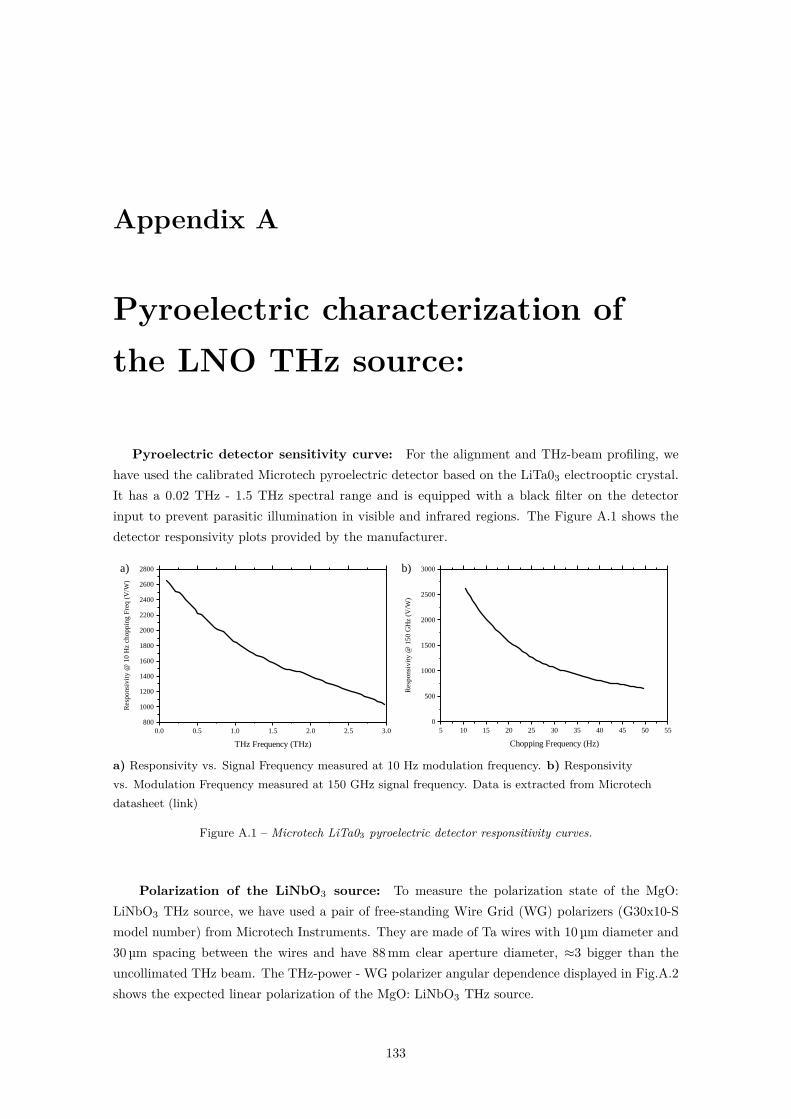
Appendix A
Pyroelectric characterization ofthe LNO THz source:
Pyroelectric detector sensitivity curve: For the alignment and THz-beam profiling, wehave used the calibrated Microtech pyroelectric detector based on the LiTa03 electrooptic crystal.It has a 0.02 THz - 1.5 THz spectral range and is equipped with a black filter on the detectorinput to prevent parasitic illumination in visible and infrared regions. The Figure A.1 shows thedetector responsivity plots provided by the manufacturer.
0 . 0 0 . 5 1 . 0 1 . 5 2 . 0 2 . 5 3 . 08 0 0
1 0 0 01 2 0 01 4 0 01 6 0 01 8 0 02 0 0 02 2 0 02 4 0 02 6 0 02 8 0 0
5 1 0 1 5 2 0 2 5 3 0 3 5 4 0 4 5 5 0 5 50
5 0 0
1 0 0 0
1 5 0 0
2 0 0 0
2 5 0 0
3 0 0 0
Respo
nsivit
y @ 10
Hz ch
opping
Freq
(V/W
)
T H z F r e q u e n c y ( T H z )
a )
Respo
nsivit
y @ 15
0 GHz
(V/W
)
C h o p p i n g F r e q u e n c y ( H z )
b )
a) Responsivity vs. Signal Frequency measured at 10 Hz modulation frequency. b) Responsivityvs. Modulation Frequency measured at 150 GHz signal frequency. Data is extracted from Microtechdatasheet (link)
Figure A.1 – Microtech LiTa03 pyroelectric detector responsitivity curves.
Polarization of the LiNbO3 source: To measure the polarization state of the MgO:LiNbO3 THz source, we have used a pair of free-standing Wire Grid (WG) polarizers (G30x10-Smodel number) from Microtech Instruments. They are made of Ta wires with 10 µm diameter and30 µm spacing between the wires and have 88 mm clear aperture diameter, ≈3 bigger than theuncollimated THz beam. The THz-power - WG polarizer angular dependence displayed in Fig.A.2shows the expected linear polarization of the MgO: LiNbO3 THz source.
133
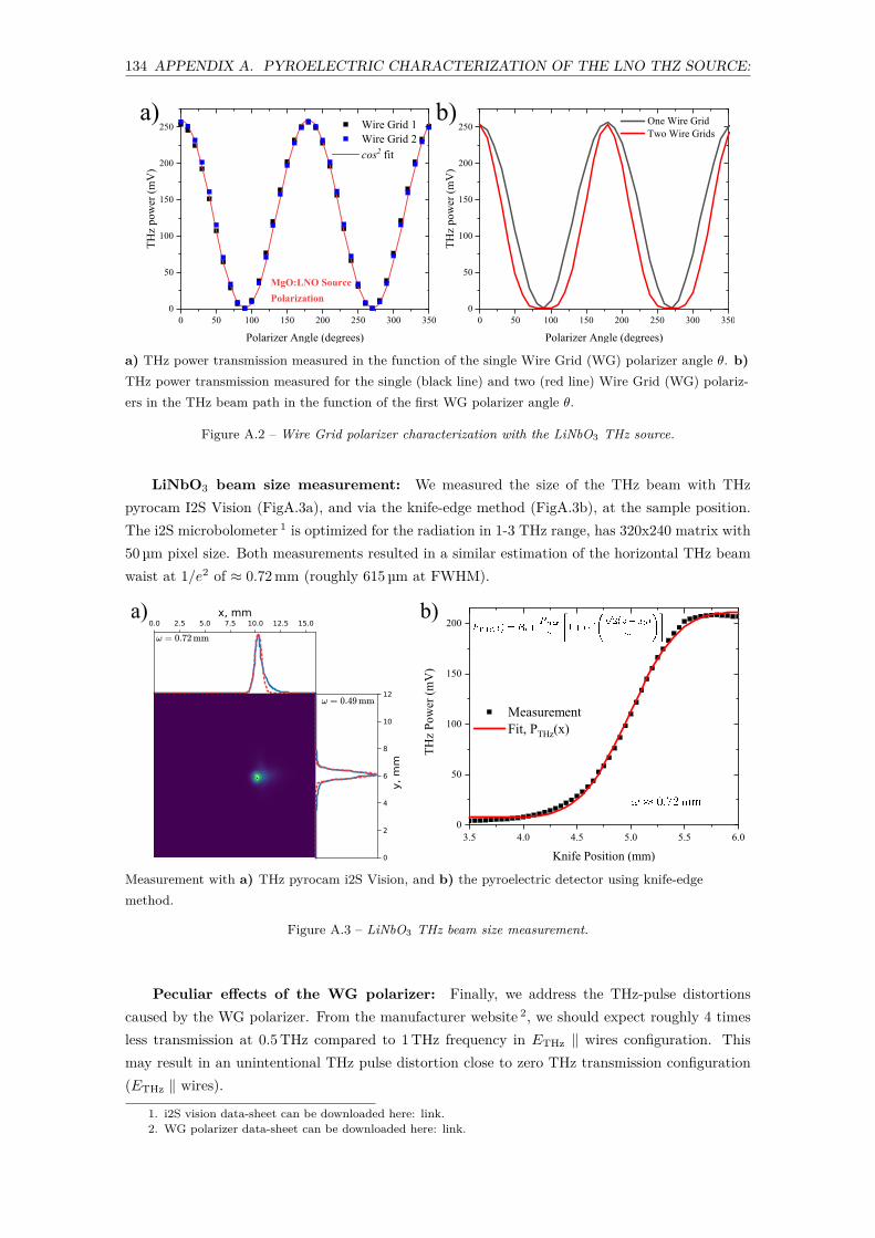
134 APPENDIX A. PYROELECTRIC CHARACTERIZATION OF THE LNO THZ SOURCE:
a) THz power transmission measured in the function of the single Wire Grid (WG) polarizer angle θ. b)THz power transmission measured for the single (black line) and two (red line) Wire Grid (WG) polariz-ers in the THz beam path in the function of the first WG polarizer angle θ.
Figure A.2 – Wire Grid polarizer characterization with the LiNbO3 THz source.
LiNbO3 beam size measurement: We measured the size of the THz beam with THzpyrocam I2S Vision (FigA.3a), and via the knife-edge method (FigA.3b), at the sample position.The i2S microbolometer 1 is optimized for the radiation in 1-3 THz range, has 320x240 matrix with50 µm pixel size. Both measurements resulted in a similar estimation of the horizontal THz beamwaist at 1/e2 of ≈ 0.72 mm (roughly 615 µm at FWHM).
Measurement with a) THz pyrocam i2S Vision, and b) the pyroelectric detector using knife-edgemethod.
Figure A.3 – LiNbO3 THz beam size measurement.
Peculiar effects of the WG polarizer: Finally, we address the THz-pulse distortionscaused by the WG polarizer. From the manufacturer website 2, we should expect roughly 4 timesless transmission at 0.5 THz compared to 1 THz frequency in ETHz ∥ wires configuration. Thismay result in an unintentional THz pulse distortion close to zero THz transmission configuration(ETHz ∥ wires).
1. i2S vision data-sheet can be downloaded here: link.2. WG polarizer data-sheet can be downloaded here: link.

135 APPENDIX A. PYROELECTRIC CHARACTERIZATION OF THE LNO THZ SOURCE:
Normalized a) LNO THz waveform measured for the different THz power, and its b) spectra. Inset isthe measurement layout.
Figure A.4 – Peculiar effects of the WG polarizer.
To investigate the WG frequency-dependent THz transmission, we have introduced the WGpolarizer and analyzer in the THz beam path, as shown in the inset of Fig.A.4a. We then measuredthe THz waveform with 200 µm thick GaP crystal, as the function of the WG polarizer angle 3.As seen from blue and red curves in Figure A.4a and b, THz gets highly distorted close to ETHz ∥WG wires configuration. In the Chapter 3 the lowest THz power was higher than 25 mV pk-pk,for which the THz pulse distortions are negligible (see A.4b).
3. See Figure A.2 for WG Polarizer - THz power correspondence.

136 APPENDIX A. PYROELECTRIC CHARACTERIZATION OF THE LNO THZ SOURCE:

Appendix B
Cr and Bi2Te3 THz-spectrumdependent residuals
a) Transient optical transmission obtained with a THz excitation for a thin Cr film. Dash-dot linescorrespond to the |ETHz|2 (red) and Wabs (blue). b) Same as a), but in the Fourier space. Data wasnormalized to overlap in the 1-2 THz range.
Figure B.1 – Short time delays: Transient response of a thin Cr film and THz pulses vs absorbed THzpower.
From the main text, we concluded that the "sideband" observed close to the natural frequency ofthe A1
1g coherent phonon mode could be attributed to the "electronic" background of the signal, andis not related to excitation of a coherent phonon. To support this claim we present here the shorttime scale signal of 14 nm Chromium film discussed in the first part of a Chapter 3. We remind thatChromium does not have optical phonon, so we should not expect any additional high-frequencycontributions to the time-delay zero signal. The δT/T signal reveals the "double bump" aroundthe time delay zero, shown as the black line in Figure B.1a. In addition, the approximate shapeof the WAbs.
THz (calculated with Eq.3.19) overlaps nicely with the δT/T signal around time delayzero (see blue line in Figure B.1a). Finally, Figure B.1b shows that difference and sum frequencycomponents of the ETHz are present in the FFT of Chromium δT/T (black), WAbs.
THz (blue dash-dot)and E2
THz (red dash-dot). This effect could be attributed to the THz-induced optical birefringenceobserved in liquids [178], transparent media [123] and metals [282].
137
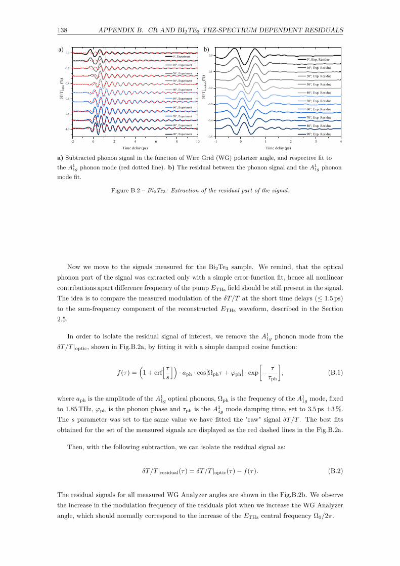
138 APPENDIX B. CR AND BI2TE3 THZ-SPECTRUM DEPENDENT RESIDUALS
a) Subtracted phonon signal in the function of Wire Grid (WG) polarizer angle, and respective fit tothe A1
1g phonon mode (red dotted line). b) The residual between the phonon signal and the A11g phonon
mode fit.
Figure B.2 – Bi2Te3: Extraction of the residual part of the signal.
Now we move to the signals measured for the Bi2Te3 sample. We remind, that the opticalphonon part of the signal was extracted only with a simple error-function fit, hence all nonlinearcontributions apart difference frequency of the pump ETHz field should be still present in the signal.The idea is to compare the measured modulation of the δT/T at the short time delays (≤ 1.5 ps)to the sum-frequency component of the reconstructed ETHz waveform, described in the Section2.5.
In order to isolate the residual signal of interest, we remove the A11g phonon mode from the
δT/T |optic, shown in Fig.B.2a, by fitting it with a simple damped cosine function:
f(τ) =(
1 + erf[τs
])· aph · cos[Ωphτ + φph] · exp
[− τ
τph
], (B.1)
where aph is the amplitude of the A11g optical phonons, Ωph is the frequency of the A1
1g mode, fixedto 1.85 THz, φph is the phonon phase and τph is the A1
1g mode damping time, set to 3.5 ps ±3 %.The s parameter was set to the same value we have fitted the "raw" signal δT/T . The best fitsobtained for the set of the measured signals are displayed as the red dashed lines in the Fig.B.2a.
Then, with the following subtraction, we can isolate the residual signal as:
δT/T |residual(τ) = δT/T |optic(τ) − f(τ). (B.2)
The residual signals for all measured WG Analyzer angles are shown in the Fig.B.2b. We observethe increase in the modulation frequency of the residuals plot when we increase the WG Analyzerangle, which should normally correspond to the increase of the ETHz central frequency Ω0/2π.
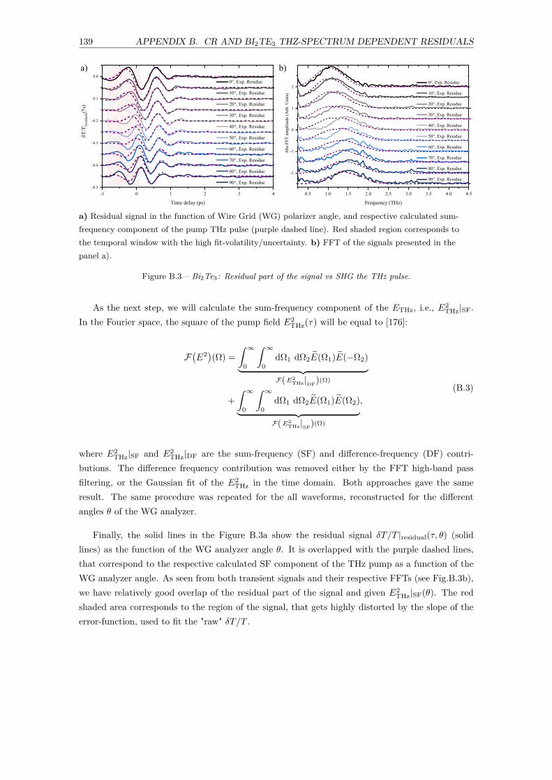
139 APPENDIX B. CR AND BI2TE3 THZ-SPECTRUM DEPENDENT RESIDUALS
a) Residual signal in the function of Wire Grid (WG) polarizer angle, and respective calculated sum-frequency component of the pump THz pulse (purple dashed line). Red shaded region corresponds tothe temporal window with the high fit-volatility/uncertainty. b) FFT of the signals presented in thepanel a).
Figure B.3 – Bi2Te3: Residual part of the signal vs SHG the THz pulse.
As the next step, we will calculate the sum-frequency component of the ETHz, i.e., E2THz|SF.
In the Fourier space, the square of the pump field E2THz(τ) will be equal to [176]:
F(E2)(Ω) =
∫ ∞
0
∫ ∞
0dΩ1 dΩ2E(Ω1)E(−Ω2)︸ ︷︷ ︸F( E2
THz|DF)(Ω)
+∫ ∞
0
∫ ∞
0dΩ1 dΩ2E(Ω1)E(Ω2)︸ ︷︷ ︸
F( E2THz|SF)(Ω)
,
(B.3)
where E2THz|SF and E2
THz|DF are the sum-frequency (SF) and difference-frequency (DF) contri-butions. The difference frequency contribution was removed either by the FFT high-band passfiltering, or the Gaussian fit of the E2
THz in the time domain. Both approaches gave the sameresult. The same procedure was repeated for the all waveforms, reconstructed for the differentangles θ of the WG analyzer.
Finally, the solid lines in the Figure B.3a show the residual signal δT/T |residual(τ, θ) (solidlines) as the function of the WG analyzer angle θ. It is overlapped with the purple dashed lines,that correspond to the respective calculated SF component of the THz pump as a function of theWG analyzer angle. As seen from both transient signals and their respective FFTs (see Fig.B.3b),we have relatively good overlap of the residual part of the signal and given E2
THz|SF(θ). The redshaded area corresponds to the region of the signal, that gets highly distorted by the slope of theerror-function, used to fit the "raw" δT/T .

140 APPENDIX B. CR AND BI2TE3 THZ-SPECTRUM DEPENDENT RESIDUALS

Appendix C
STEs Light absorption
In this appendix, we present the numerical simulations of the light absorption profiles in the setof the spintronic emitters CoFeB(5 and 20)/Pt(3) and CoFeB(5 and 20)/MgO(6), where numberin brackets is the thickness of the layer in nm. Calculations are done using the Transfer MatrixMethod approach, discussed in the Section 1.3.2. For the CoFeB nanolayers, the optical constantwere extracted from the work of X.Liang et.al [283]. For Pt, we used the data from Rakic et.al. [156].
The plots presented in this appendix are shown in terms of the fraction of absorbed opticalpower per unit of the distance (nm). The amount of the absorbed optical power Aabs within thelayer i of the thickness d was calculated as following:
Aiabs =
∑n A
nabs(dn)Atot
inc, (C.1)
where n is the discrete value of the absorbed optical power per unit of distance within the rangedi−1≤dn≤di+1, and P tot
inc is total incident optical power. The data for the Back and Front Faceexcitations are shown in the Table C.1
The light absorption gradient ∇Az was estimated using this equation:
∇Az = Aabs(0) −Aabs(d)d
, (C.2)
Front BackFM FM Si
CoFeB(5)Pt(3) 35% 10% 33%CoFeB(20)Pt(3) 44% 19% 12.40%
CoFeB(5)MgO(6) 48.80% 13.60% 43.20%CoFeB(20)MgO(6) 50.70% 24.10% 15.60%
Table C.1 – Absorbed power in the CoFeB for the Front (SiO2) and Back (Si) configurations
141
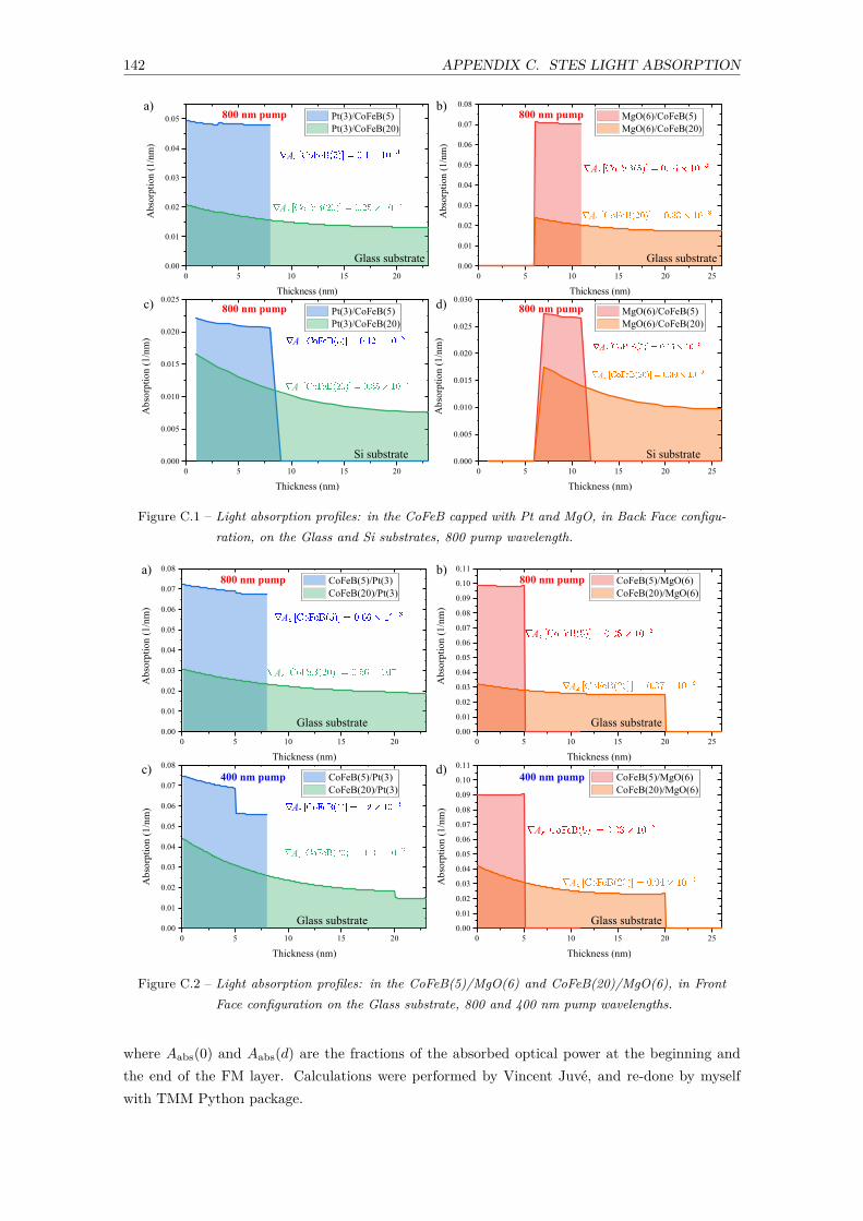
142 APPENDIX C. STES LIGHT ABSORPTION
Figure C.1 – Light absorption profiles: in the CoFeB capped with Pt and MgO, in Back Face configu-ration, on the Glass and Si substrates, 800 pump wavelength.
Figure C.2 – Light absorption profiles: in the CoFeB(5)/MgO(6) and CoFeB(20)/MgO(6), in FrontFace configuration on the Glass substrate, 800 and 400 nm pump wavelengths.
where Aabs(0) and Aabs(d) are the fractions of the absorbed optical power at the beginning andthe end of the FM layer. Calculations were performed by Vincent Juvé, and re-done by myselfwith TMM Python package.
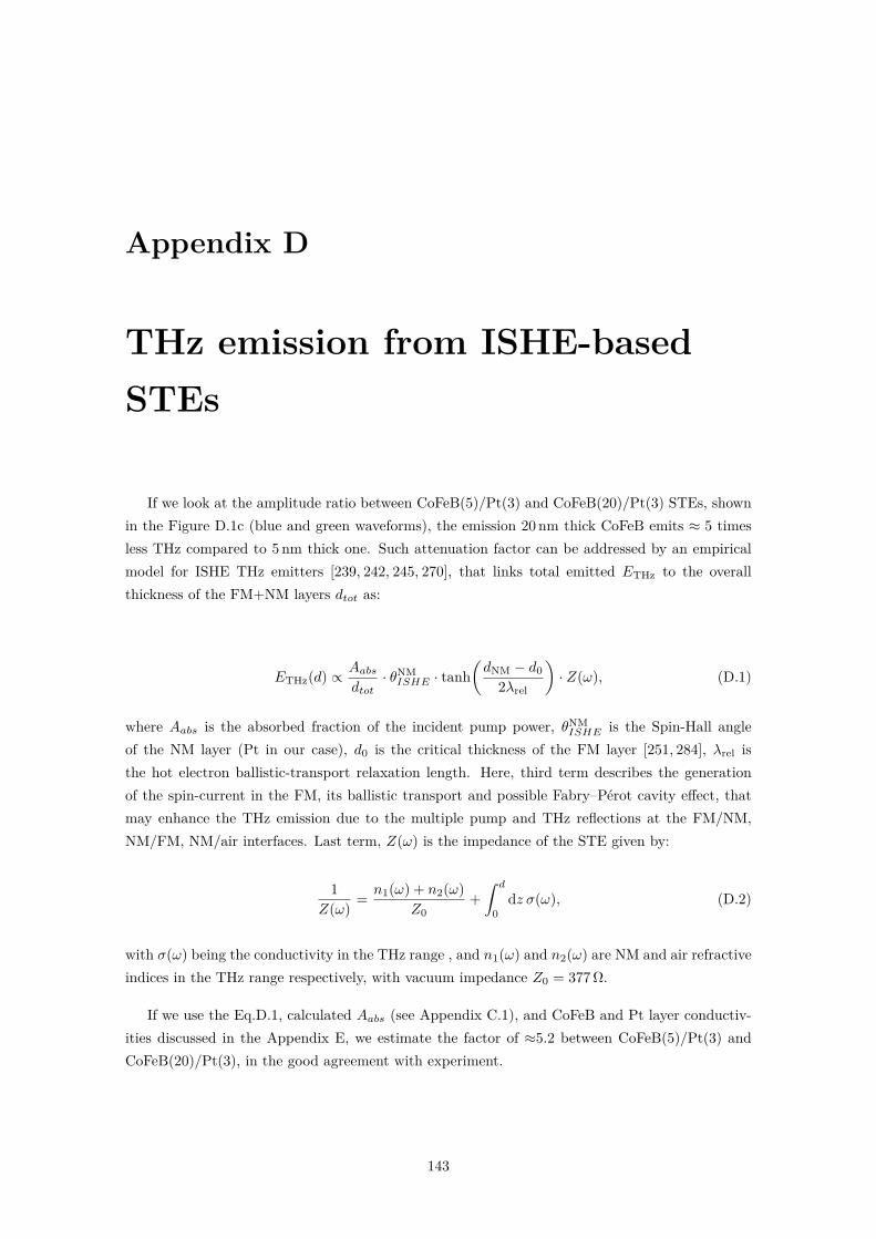
Appendix D
THz emission from ISHE-basedSTEs
If we look at the amplitude ratio between CoFeB(5)/Pt(3) and CoFeB(20)/Pt(3) STEs, shownin the Figure D.1c (blue and green waveforms), the emission 20 nm thick CoFeB emits ≈ 5 timesless THz compared to 5 nm thick one. Such attenuation factor can be addressed by an empiricalmodel for ISHE THz emitters [239, 242, 245, 270], that links total emitted ETHz to the overallthickness of the FM+NM layers dtot as:
ETHz(d) ∝ Aabs
dtot· θNM
ISHE · tanh(dNM − d0
2λrel
)· Z(ω), (D.1)
where Aabs is the absorbed fraction of the incident pump power, θNMISHE is the Spin-Hall angle
of the NM layer (Pt in our case), d0 is the critical thickness of the FM layer [251, 284], λrel isthe hot electron ballistic-transport relaxation length. Here, third term describes the generationof the spin-current in the FM, its ballistic transport and possible Fabry–Pérot cavity effect, thatmay enhance the THz emission due to the multiple pump and THz reflections at the FM/NM,NM/FM, NM/air interfaces. Last term, Z(ω) is the impedance of the STE given by:
1Z(ω) = n1(ω) + n2(ω)
Z0+∫ d
0dz σ(ω), (D.2)
with σ(ω) being the conductivity in the THz range , and n1(ω) and n2(ω) are NM and air refractiveindices in the THz range respectively, with vacuum impedance Z0 = 377 Ω.
If we use the Eq.D.1, calculated Aabs (see Appendix C.1), and CoFeB and Pt layer conductiv-ities discussed in the Appendix E, we estimate the factor of ≈5.2 between CoFeB(5)/Pt(3) andCoFeB(20)/Pt(3), in the good agreement with experiment.
143
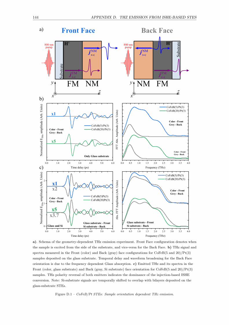
144 APPENDIX D. THZ EMISSION FROM ISHE-BASED STES
a). Schema of the geometry-dependent THz emission experiment. Front Face configuration denotes whenthe sample is excited from the side of the substrate, and vice-versa for the Back Face. b) THz signal andspectra measured in the Front (color) and Back (gray) face configurations for CoFeB(5 and 20)/Pt(3)samples deposited on the glass substrate. Temporal delay and waveform broadening for the Back Faceorientation is due to the frequency dependent Glass absorption. c) Emitted THz and its spectra in theFront (color, glass substrate) and Back (gray, Si substrate) face orientation for CoFeB(5 and 20)/Pt(3)samples. THz polarity reversal of both emitters indicates the dominance of the injection-based ISHEconversion. Note: Si-substrate signals are temporally shifted to overlap with bilayers deposited on theglass-substrate STEs.
Figure D.1 – CoFeB/Pt STEs: Sample orientation dependent THz emission.

Appendix E
THz-TDS of the Pt- andMgO-based spintronic emitters
From the discussion of the THz emission in the Back Face configuration, in the absence ofthe substrate THz absorption, Torosyan et.al. [251] proposed to introduce an additional term intoEq.D.1, which accounts for the THz attenuation due to the propagation through the metal layerstack :
κTHz = exp[−dF M + dNM
ξTHz
], (E.1)
where ξTHz is the effective inverse attenuation coefficient of the THz radiation, proposed by theauthors. We can experimentally check this model, since this term can be effectively measured bythe means of THz-TDS.
In order to check the validity the latter equation, we performed simple THz-TDS spectroscopyon the set of the spintronic emitters. For this experiment, we recorded the THz pulse that propa-gates through the bare 500 µm silicone substrate Sref (t), and via FFT we extract the informationabout its spectral components, Sref (ω). After, the 500 µm silicone substrate was replaced by theCoFeB(5 and 20)/Pt(3) grown on the 300 µm silicone substrate, and we recorded Ssam(t) withSsam(ω).
In the Fig.E.1a, we show the ratio between of the FFT magnitudes of Ssam(ω) and Sref (ω),showing the ETHz amplitude transmission through given sample. The fringes observed in theFig.E.1a and Fig.E.2a may correspond to the Fabry-Pérot effect induced by the thickness differ-ence of the reference and sample silicone substrates. The data for CoFeB(∆15) was obtained bytaking the THz transmission from CoFeB(5)/Pt(3) as Sref (ω), and CoFeB(20)/Pt(3) as Ssam(ω).THz transmission for all the samples show nearly frequency independent behaviour, well in theagreement with previous reports [100].
With Eq.E.1 with constant ξTHz it is not possible to explain the measured THz attenuationfactor, underlying the thickness and layer-dependent THz conductivity of the whole metal stack.We then change the the Eq.E.1 by accounting for the thickness change of the specific layer, which
145
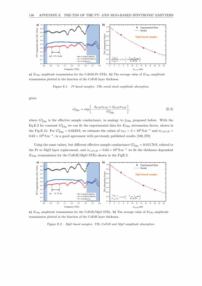
146 APPENDIX E. THZ-TDS OF THE PT- AND MGO-BASED SPINTRONIC EMITTERS
a) ETHz amplitude transmission for the CoFeB/Pt STEs. b) The average value of ETHz amplitudetransmission plotted in the function of the CoFeB layer thickness.
Figure E.1 – Pt based samples: THz metal stack amplitude absorption.
gives:
κ∗THz = exp
[−dF MσF M + dNMσNM
G∗THz
], (E.2)
where G∗THz is the effective sample conductance, in analogy to ξTHz proposed before. With the
Eq.E.2 for constant G∗THz we can fit the experimental data for ETHz attenuation factor, shown in
the Fig.E.1b. For G∗THz = 0.0233 S, we estimate the values of σP t = 3 × 10⁶ S m−1 and σCoF eB =
0.63 × 10⁶ S m−1, in a good agreement with previously published results [100,270].
Using the same values, but different effective sample conductance G∗THz = 0.015 78 S, related to
the Pt to MgO layer replacement, and σCoF eB = 0.63 × 10⁶ S m−1 we fit the thickness dependentETHz transmission for the CoFeB/MgO STEs shown in the FigE.2.
a) ETHz amplitude transmission for the CoFeB/MgO STEs. b) The average value of ETHz amplitudetransmission plotted in the function of the CoFeB layer thickness.
Figure E.2 – MgO based samples: THz CoFeB and MgO amplitude absorption.

Appendix F
Appendix: STEs’ emitted THzfield amplitude - pump powerdependence
Power/THz amplitude dependence. First and Second batches: In order to checkthe sample growth repeatability process, we have two batches of the same spintronic bilayers,grown on the float-zone glass substrate. We then measured the ETHz amplitude - pump fluence Φdependence for all the samples discussed in this manuscript.
The ETHz pump power-dependence of the CoFeB/Pt samples is shown on the Figure F.1a. Theobserved nonlinear ETHz increase for CoFeB layers with 5 and 20 nm thickness can be attributedto both saturation of the magnetization quenching [275] and spin-trapping inside the HM layer [3].At this stage, however, we cannot separate these two effects. Nevertheless, we show rather goodconsistency between the two batches, with ETHz peak-to-peak difference of about 20 %, that canbe attributed to the CoFeB or Pt layer thickness incertitude, which highly affects spin-to-chargeconversion efficiency [251].
Figure F.1b depicts the ETHz - Φ dependence of the CoFeB(20)/MgO(5 and 6) samples. Thesesamples show better consistency, with the ETHz peak-to-peak difference of less than 10 %.
At last, Fig.F.1 shows the data for CoFeB(5)/MgO(5)/Ta(2) and CoFeB(5)/MgO(6) STEs.Similar ETHz - Φ dependence, and THz waveform of these two samples indicates that the Rashbastates are not affected by the deposition of the metallic layer on top of MgO film. Lower THz peak-to-peak amplitudes for CoFeB(5)/MgO(5)/Ta(2) can be partially attributed to the additional THzabsorption in the 2 nm Ta layer. The deposition of the thin metallic layer on top of the MgOcould positively impact the damage threshold of the CoFeB/MgO Rashba states, which could beinteresting to address in the future.
Pump-power dependent Si THz absorption: In order to better understand the powerdependence of the STE in the Back and Front Face configurations, we have measured the depen-dence of the THz pulse transmission through photoexcited Si wafer. To simulate the Back-Face
147
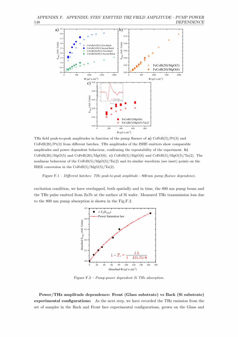
148APPENDIX F. APPENDIX: STES’ EMITTED THZ FIELD AMPLITUDE - PUMP POWER
DEPENDENCE
THz field peak-to-peak amplitudes in function of the pump fluence of a) CoFeB(5)/Pt(3) andCoFeB(20)/Pt(3) from different batches. THz amplitudes of the ISHE emitters show comparableamplitudes and power dependent behaviour, confirming the repeatability of the experiment. b)CoFeB(20)/MgO(5) and CoFeB(20)/MgO(6). c) CoFeB(5)/MgO(6) and CoFeB(5)/MgO(5)/Ta(2). Thenonlinear behaviour of the CoFeB(5)/MgO(5)/Ta(2) and its similar waveform (see inset) points on theIREE conversion in the CoFeB(5)/MgO(5)/Ta(2).
Figure F.1 – Different batches: THz peak-to-peak amplitude - 800 nm pump fluence dependence.
excitation condition, we have overlapped, both spatially and in time, the 800 nm pump beam andthe THz pulse emitted from ZnTe at the surface of Si wafer. Measured THz transmission loss dueto the 800 nm pump absorption is shown in the Fig.F.2.
Figure F.2 – Pump-power dependent Si THz absorption.
Power/THz amplitude dependence: Front (Glass substrate) vs Back (Si substrate)experimental configurations: As the next step, we have recorded the THz emission from theset of samples in the Back and Front face experimental configurations, grown on the Glass and

149APPENDIX F. APPENDIX: STES’ EMITTED THZ FIELD AMPLITUDE - PUMP POWER
DEPENDENCE
Si substrates. Figure F.3 shows the peak-to-peak ETHz amplitude in function of the FM layerabsorbed laser fluence Φabs. We see the highly nonlinear THz absorption as a function of the800 nm pump fluence. This complicates the retrieval of the real STE THz amplitudes in the BackFace configuration for the samples grown on the Si substrate.
THz field peak-to-peak amplitudes in function of the pump fluence of a) CoFeB(5)/Pt(3) andCoFeB(20)/Pt(3) from different batches. THz amplitudes of the ISHE emitters show comparableamplitudes and power dependent behaviour, confirming the repeatability of the experiment. b)CoFeB(20)/MgO(5) and CoFeB(20)/MgO(6). c) CoFeB(5)/MgO(6) and CoFeB(5)/MgO(5)/Ta(2). Thenonlinear behaviour of the CoFeB(5)/MgO(5)/Ta(2) and its similar waveform (see inset) points on theIREE conversion in the CoFeB(5)/MgO(5)/Ta(2).
Figure F.3 – Glass and Si substrates: THz amplitude versus FM absorbed fluence.
Let us take a look first at the CoFeB/Pt based samples. For the CoFeB(5)/Pt(3) (see Fig.F.3a),the Back Face configuration 1 is less efficient than the Front Face one 2, which is due to the power-dependent Si THz absorption, addressed in the previous paragraph.
On the other hand, for the same amount of the pump fluence absorbed by the CoFeB, THzemission from CoFeB(20)/Pt(3) in Back Face configuration is more efficient than the Front Faceexcitation, without even accounting for the Si photoexcitation loss. This could be related to thenon-equivalent spin injection into the HM between the Back and Front face excitations, and itneeds to be confirmed with first principle calculations. Importantly, the data for the Back Faceexcitation does not account for the THz absorption in the CoFeB and photoexcited Si.
Next, the same measurement done for the CoFeB(5)/MgO(6) sample (see FigF.3c). The FrontFace ETHz pump fluence dependence of this sample was already discussed in the main text. Inter-estingly, the efficiency of the CoFeB(5)/MgO(6) THz emission looks like the inverse of the FrontFace data, despite the fluence dependent Si absorption. Such evolution of the ETHz amplitude
1. Excitation from the side of the non-magnetic layer.2. Excitation from the side of the substrate.
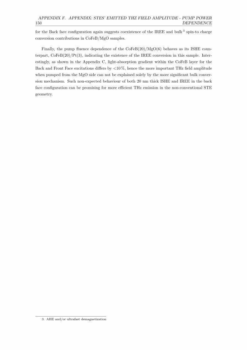
150APPENDIX F. APPENDIX: STES’ EMITTED THZ FIELD AMPLITUDE - PUMP POWER
DEPENDENCE
for the Back face configuration again suggests coexistence of the IREE and bulk 3 spin-to chargeconversion contributions in CoFeB/MgO samples.
Finally, the pump fluence dependence of the CoFeB(20)/MgO(6) behaves as its ISHE coun-terpart, CoFeB(20)/Pt(3), indicating the existence of the IREE conversion in this sample. Inter-estingly, as shown in the Appendix C, light-absorption gradient within the CoFeB layer for theBack and Front Face excitations differs by <10 %, hence the more important THz field amplitudewhen pumped from the MgO side can not be explained solely by the more significant bulk conver-sion mechanism. Such non-expected behaviour of both 20 nm thick ISHE and IREE in the backface configuration can be promising for more efficient THz emission in the non-conventional STEgeometry.
3. AHE and/or ultrafast demagnetization
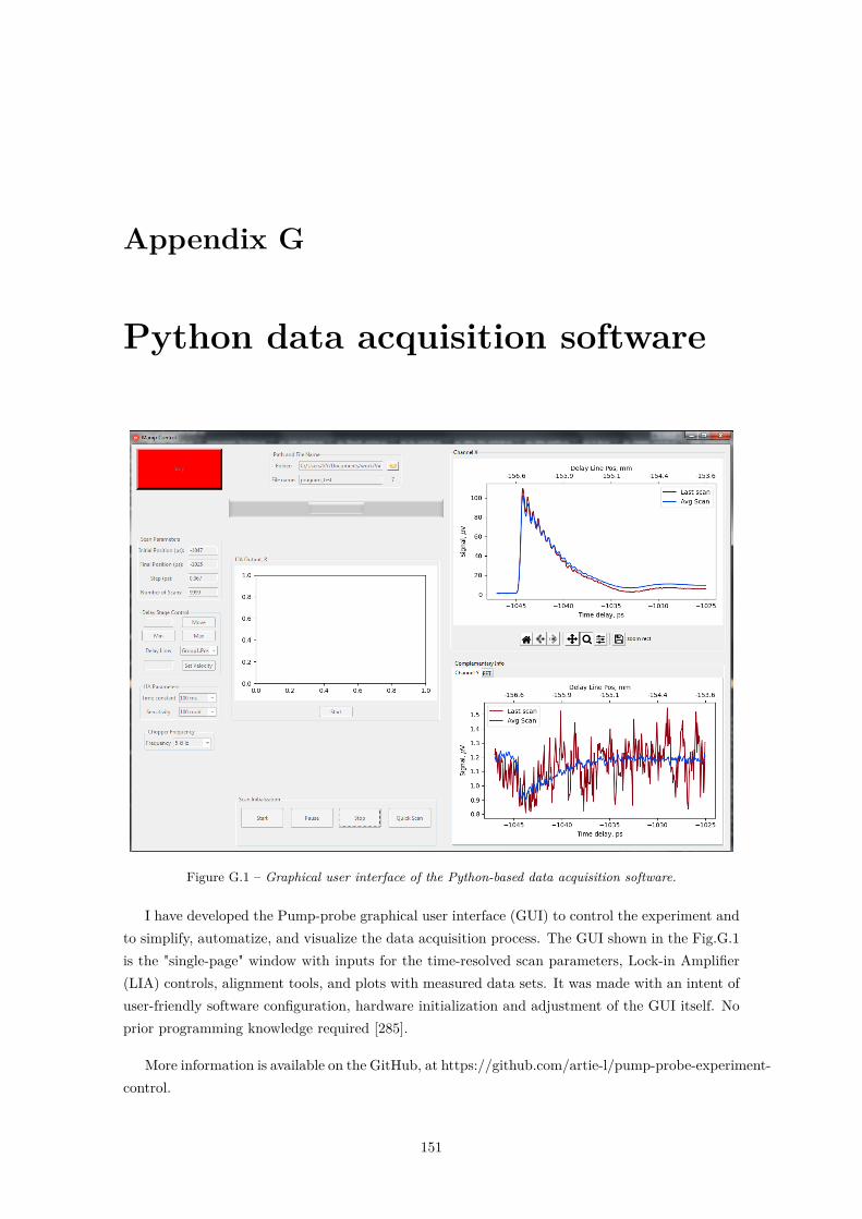
Appendix G
Python data acquisition software
Figure G.1 – Graphical user interface of the Python-based data acquisition software.
I have developed the Pump-probe graphical user interface (GUI) to control the experiment andto simplify, automatize, and visualize the data acquisition process. The GUI shown in the Fig.G.1is the "single-page" window with inputs for the time-resolved scan parameters, Lock-in Amplifier(LIA) controls, alignment tools, and plots with measured data sets. It was made with an intent ofuser-friendly software configuration, hardware initialization and adjustment of the GUI itself. Noprior programming knowledge required [285].
More information is available on the GitHub, at https://github.com/artie-l/pump-probe-experiment-control.
151

152 APPENDIX G. PYTHON DATA ACQUISITION SOFTWARE
Bibliography
[1] Tobias Kampfrath, Koichiro Tanaka, and Keith A. Nelson. Resonant and nonresonant controlover matter and light by intense terahertz transients. Nature Photonics, 7(9):680–690, 9 2013.
[2] M. Först, R. Mankowsky, and A. Cavalleri. Mode-Selective Control of the Crystal Lattice.Accounts of Chemical Research, 48(2):380–387, 2 2015.
[3] T. Kampfrath, M. Battiato, P. Maldonado, G. Eilers, J. Nötzold, S. Mährlein, V. Zbarsky,F. Freimuth, Y. Mokrousov, S. Blügel, M. Wolf, I. Radu, P. M. Oppeneer, and M. Münzen-berg. Terahertz spin current pulses controlled by magnetic heterostructures. Nature Nan-otechnology, 8(4):256–260, 4 2013.
[4] Olivier Rousseau, Cosimo Gorini, Fatima Ibrahim, Jean-Yves Chauleau, Aurélie Solignac,Ali Hallal, Sebastian Tölle, Mairbek Chshiev, and Michel Viret. Spin-charge conversion inferromagnetic Rashba states. Physical Review B, 104(13):134438, 10 2021.
[5] Michael Eckert. Disputed discovery: the beginnings of X-ray diffraction in crystals in 1912and its repercussions. Acta Crystallographica Section A Foundations of Crystallography,68(1):30–39, 1 2012.
[6] Richard J. D. Tilley. Understanding Solids. John Wiley & Sons, Ltd, Chichester, UK, 72004.
[7] Charles Kittel. Introduction to Solid State Physics. John Wiley and Sons, 7th edition, 61996.
[8] N. Vagelatos, D. Wehe, and J. S. King. Phonon dispersion and phonon densities of states forZnS and ZnTe. The Journal of Chemical Physics, 60(9):3613–3618, 5 1974.
[9] Neil W. Ashcroft, N. David Mermin, and Sergio Rodriguez. Solid State Physics. CRC Press,1 1978.
[10] James E. Bernard and Alex Zunger. Electronic structure of ZnS, ZnSe, ZnTe, and theirpseudobinary alloys. Physical Review B, 36(6):3199–3228, 8 1987.
[11] J. M. D. Coey. Magnetism and Magnetic Materials. Cambridge University Press, 1 2001.
[12] Walther Gerlach and Otto Stern. Der experimentelle Nachweis der Richtungsquantelung imMagnetfeld. Zeitschrift fur Physik, 9(1):349–352, 12 1922.
[13] Robert M. White. Quantum Theory of Magnetism : Magnetic Properties of Materials.Springer Berlin Heidelberg, 2007.
[14] Paul Adrien Maurice Dirac. The quantum theory of the electron. Proceedings of the RoyalSociety of London. Series A, Containing Papers of a Mathematical and Physical Character,117(778):610–624, 2 1928.
153
154 BIBLIOGRAPHY
[15] Albert A. Michelson. XXX. On the application of interference methods to spectroscopic mea-surements. —II. The London, Edinburgh, and Dublin Philosophical Magazine and Journalof Science, 34(208):280–299, 9 1892.
[16] Wolfgang Nolting and Anupuru Ramakanth. Quantum theory of magnetism, volume 53.Springer Berlin Heidelberg, Berlin, Heidelberg, 2 2009.
[17] Joachim Stöhr and Hans Christoph Siegmann. Magnetism: From fundamentals to nanoscaledynamics, volume 152. Springer Berlin Heidelberg, Berlin, Heidelberg, 2006.
[18] Yehuda B. Band and Yshai Avishai. Electronic Properties of Solids. In Quantum Mechanicswith Applications to Nanotechnology and Information Science, pages 381–544. Elsevier, 2013.
[19] N. F. Mott. A discussion of the transition metals on the basis of quantum mechanics.Proceedings of the Physical Society, 47(4):571–588, 1935.
[20] J. C. Slater. The Ferromagnetism of Nickel. Physical Review, 49(7):537–545, 4 1936.
[21] E C Stoner. Collective electron ferronmagnetism. Proceedings of the Royal Society of London.Series A. Mathematical and Physical Sciences, 165(922):372–414, 4 1938.
[22] A.Y. Morsy, S.S. Fouad, E. Hashem, and A.A. El-Shazly. Optical Properties of ThermallyDeposited Bismuth Telluride in the Wavelength Range of 2.5-10 µm. Acta Physica PolonicaA, 80(6):819–825, 1991.
[23] Robert W. Boyd. Nonlinear Optics. Elsevier, 4th edition, 2020.
[24] Peter Y. Yu and Manuel Cardona. Fundamentals of Semiconductors, volume 28 of GraduateTexts in Physics. Springer Berlin Heidelberg, Berlin, Heidelberg, 4 edition, 2010.
[25] Martin Dressel and George Grüner. Electrodynamics of Solids. Cambridge University Press,1 2002.
[26] P. B. Johnson and R. W. Christy. Optical Constant of the Nobel Metals. Physical ReviewB, 6(12):4370–4379, 1972.
[27] W Lynch and R Rosei. Thermomodulation Spectra of Al, Au, and Cu. Physical Review B,5(10):3883–3894, 1972.
[28] R. Rosei. Temperature modulation of the optical transitions involving the fermi surface inAg: Theory. Physical Review B, 10(2):474–483, 1974.
[29] M. Guerrisi, R. Rosei, and P. Winsemius. Splitting of the interband absorption edge in Au.Physical Review B, 12(2):557–563, 1975.
[30] T O Otomalo. Ultrafast optical response of complex plasmonic nanoparticles. PhD thesis,Université Paris-Saclay, 2018.
[31] J Lindhard. On the properites of a gas of charged particles. Dan. Mat. Phys. Medd., 28:8,1954.
[32] James D Patterson and Bernard C Bailey. Solid-State Physics. Springer International Pub-lishing, Cham, 2018.
[33] Kohzo Sato and Sadao Adachi. Optical properties of ZnTe. Journal of Applied Physics,73(2):926–931, 1 1993.
[34] A. S. Barker. Transverse and Longitudinal Optic Mode Study in Mg F2. Physical Review,136(5A):A1290–A1295, 11 1964.
[35] R. H. Lyddane, R. G. Sachs, and E. Teller. On the Polar Vibrations of Alkali Halides.Physical Review, 59(8):673–676, 4 1941.
155 BIBLIOGRAPHY
[36] Tatsumi Kurosawa. Polarization Waves in Solids. Journal of the Physical Society of Japan,16(7):1298–1308, 7 1961.
[37] A. Leitenstorfer, S. Hunsche, J. Shah, M. C. Nuss, and W. H. Knox. Detectors and sourcesfor ultrabroadband electro-optic sampling: Experiment and theory. Applied Physics Letters,74(11):1516–1518, 1999.
[38] J. Hebling, A. G. Stepanov, G. Almási, B. Bartal, and J. Kuhl. Tunable THz pulse generationby optical rectification of ultrashort laser pulses with tilted pulse fronts. Applied Physics B:Lasers and Optics, 78(5):593–599, 2004.
[39] Juejun Hu, Hongtao Lin, Okechukwu Ogbuu, Jifeng Liu, Lin Zhang, and Jurgen Michel.Breaking the energy-bandwidth limit of electro-optic modulators: theory and a device pro-posal. In CLEO: 2013, volume 31, Washington, D.C., 2013. OSA.
[40] Vincent Juvé, Gwenaëlle Vaudel, Zoltan Ollmann, Janos Hebling, Vasily Temnov, VitalyiGusev, and Thomas Pezeril. Ultrafast tunable modulation of light polarization at terahertzfrequencies. Optics Letters, 43(24):5905, 12 2018.
[41] Frank L. Pedrotti, Leno M. Pedrotti, and Leno S. Pedrotti. Introduction to Optics. CambridgeUniversity Press, 12 2017.
[42] Steven J. Byrnes. Multilayer optical calculations. arXiv, pages 1–20, 3 2016.
[43] Charalambos C. Katsidis and Dimitrios I. Siapkas. General transfer-matrix method foroptical multilayer systems with coherent, partially coherent, and incoherent interference.Applied Optics, 41(19):3978, 7 2002.
[44] Tom Sebastian Seifert. Spintronics with Terahertz Radiation : Probing and driving spins athighest frequencies. PhD thesis, Universitat Berlin, 2018.
[45] E.G. Gamaly and A.V. Rode. Physics of ultra-short laser interaction with matter: Fromphonon excitation to ultimate transformations. Progress in Quantum Electronics, 37(5):215–323, 9 2013.
[46] SI Anisimov, BL Kapeliovich, and TL Perel’man. Electron emission from metal surfacesexposed to ultrashort laser pulses. Sov. Phys. JETP, 39(2):375–377, 1974.
[47] T. Q. Qiu and C. L. Tien. Heat Transfer Mechanisms During Short-Pulse Laser Heating ofMetals. Journal of Heat Transfer, 115(4):835–841, 11 1993.
[48] E. Beaurepaire, J.-C. Merle, A. Daunois, and J.-Y. Bigot. Ultrafast Spin Dynamics inFerromagnetic Nickel. Physical Review Letters, 76(22):4250–4253, 5 1996.
[49] Jean-Yves Bigot, Mircea Vomir, and Eric Beaurepaire. Coherent ultrafast magnetism inducedby femtosecond laser pulses. Nature Physics, 5(7):515–520, 7 2009.
[50] Hyejin Jang, Luca Marnitz, Torsten Huebner, Johannes Kimling, Timo Kuschel, andDavid G. Cahill. Thermal Conductivity of Oxide Tunnel Barriers in Magnetic Tunnel Junc-tions Measured by Ultrafast Thermoreflectance and Magneto-Optic Kerr Effect Thermome-try. Physical Review Applied, 13(2):024007, 2 2020.
[51] Pui-Wai Ma, S. L. Dudarev, and C. H. Woo. Spin-lattice-electron dynamics simulations ofmagnetic materials. Physical Review B, 85(18):184301, 5 2012.
[52] Aryan Navabi, Cai Chen, Anthony Barra, Mohsen Yazdani, Guoqiang Yu, Mohammad Mon-tazeri, Mohammed Aldosary, Junxue Li, Kin Wong, Qi Hu, Jing Shi, Gregory P Carman,
156 BIBLIOGRAPHY
Abdon E Sepulveda, Pedram Khalili Amiri, and Kang L Wang. Efficient Excitation of High-Frequency Exchange-Dominated Spin Waves in Periodic Ferromagnetic Structures. PhysicalReview Applied, 7(3), 2017.
[53] Xiaoyong Liu, Wenzhe Zhang, Matthew J Carter, and Gang Xiao. Ferromagnetic resonanceand damping properties of CoFeB thin films as free layers in MgO-based magnetic tunneljunctions. Journal of Applied Physics, 110(3):33910, 2011.
[54] A Conca, B Heinz, M R Schweizer, S Keller, E Th Papaioannou, and B Hillebrands. Lack ofcorrelation between the spin-mixing conductance and the inverse spin Hall effect generatedvoltages in CoFeB/Pt and CoFeB/Ta bilayers. Physical Review B, 95(17):174426, 2017.
[55] B Heinrich, C Burrowes, E Montoya, B Kardasz, E Girt, Young Yeal Song, Yiyan Sun,and Mingzhong Wu. Spin pumping at the magnetic insulator (YIG)/normal metal (Au)interfaces. Physical Review Letters, 107(6), 2011.
[56] Zhibin Lin, Leonid V. Zhigilei, and Vittorio Celli. Electron-phonon coupling and electronheat capacity of metals under conditions of strong electron-phonon nonequilibrium. PhysicalReview B, 77(7):075133, 2 2008.
[57] Niladri Chatterji, Ashwin A Tulapurkar, and Bhaskaran Muralidharan. Enhancement of spin-transfer torque switching via resonant tunneling. Applied Physics Letters, 105(23):232410,2014.
[58] Yiwen Cui, Yu Wang, Jie Wu, Xiaokang He, Shouhu Xuan, and Xinglong Gong. Magneto-thermochromic coupling Janus sphere for dual response display. RSC Advances, 9(31):17959–17966, 2019.
[59] P. M. Paul, E. S. Toma, P. Breger, G. Mullot, F. Augé, Ph Balcou, H. G. Muller, andP. Agostini. Observation of a train of attosecond pulses from high harmonic generation.Science, 292(5522):1689–1692, 2001.
[60] A. L. Cavalieri, N. Müller, Th Uphues, V. S. Yakovlev, A. Baltuška, B. Horvath, B. Schmidt,L. Blümel, R. Holzwarth, S. Hendel, M. Drescher, U. Kleineberg, P. M. Echenique, R. Kien-berger, F. Krausz, and U. Heinzmann. Attosecond spectroscopy in condensed matter. Nature,449(7165):1029–1032, 2007.
[61] I. Orfanos, I. Makos, I. Liontos, E. Skantzakis, B. Förg, D. Charalambidis, and P. Tzallas.Attosecond pulse metrology. APL Photonics, 4(8), 2019.
[62] A. M. Lindenberg, I. Kang, S. L. Johnson, T. Missalla, P. A. Heimann, Z. Chang, J. Larsson,P. H. Bucksbaum, H. C. Kapteyn, H. A. Padmore, R. W. Lee, J. S. Wark, and R. W.Falcone. Time-resolved X-ray diffraction from coherent phonons during a laser-induced phasetransition. Physical Review Letters, 84(1):111–114, 2000.
[63] Manuel Joffre. Optique non-linéaire en régimes continu et femtoseconde, 2014.
[64] Donna Strickland and Gerard Mourou. Compression of amplified chirped optical pulses.Optics Communications, 56(3):219–221, 12 1985.
[65] Q. Wu and X. C. Zhang. 7 terahertz broadband GaP electro-optic sensor. Applied PhysicsLetters, 70(14):1784–1786, 1997.
[66] H. Hirori, A. Doi, F. Blanchard, and K. Tanaka. Single-cycle terahertz pulses with amplitudesexceeding 1 MV/cm generated by optical rectification in LiNbO3. Applied Physics Letters,98(9):091106, 2 2011.
157 BIBLIOGRAPHY
[67] Arno Schneider, Max Neis, Marcel Stillhart, Blanca Ruiz, Rizwan U. A. Khan, and PeterGünter. Generation of terahertz pulses through optical rectification in organic DAST crystals:theory and experiment. Journal of the Optical Society of America B, 23(9):1822, 2006.
[68] H. Hamster, A. Sullivan, S. Gordon, W. White, and R. W. Falcone. Subpicosecond, electro-magnetic pulses from intense laser-plasma interaction. Physical Review Letters, 71(17):2725–2728, 10 1993.
[69] C. Evain, C. Szwaj, E. Roussel, J. Rodriguez, M. Le Parquier, M. A. Tordeux, F. Ribeiro,M. Labat, N. Hubert, J. B. Brubach, P. Roy, and S. Bielawski. Stable coherent terahertz syn-chrotron radiation from controlled relativistic electron bunches. Nature Physics, 15(7):635–639, 2019.
[70] G. L. Carr, Michael C. Martin, Wayne R. McKinney, K. Jordan, George R. Neil, and G. P.Williams. High-power terahertz radiation from relativistic electrons. Nature, 420(6912):153–156, 11 2002.
[71] David R. Bacon, Julien Madéo, and Keshav M. Dani. Photoconductive emitters for pulsedterahertz generation. Journal of Optics (United Kingdom), 23(6), 2021.
[72] David H. Auston and Martin C. Nuss. Electrooptic Generation and Detection of FemtosecondElectrical Transients. IEEE Journal of Quantum Electronics, 24(2):184–197, 1988.
[73] D. Grischkowsky, Søren Keiding, Martin van Exter, and Ch. Fattinger. Far-infrared time-domain spectroscopy with terahertz beams of dielectrics and semiconductors. Journal of theOptical Society of America B, 7(10):2006, 1990.
[74] P. Uhd Jepsen, R. H. Jacobsen, and S. R. Keiding. Generation and detection of terahertzpulses from biased semiconductor antennas. Journal of the Optical Society of America B,13(11):2424, 1996.
[75] Jianming Dai, Xu Xie, and X. C. Zhang. Detection of broadband terahertz waves with alaser-induced plasma in gases. Physical Review Letters, 97(10):8–11, 2006.
[76] Jingle Liu and X. C. Zhang. Terahertz-radiation-enhanced emission of fluorescence from gasplasma. Physical Review Letters, 103(23):1–4, 2009.
[77] Ajay Nahata, Aniruddha S. Weling, and Tony F. Heinz. A wideband coherent terahertzspectroscopy system using optical rectification and electro-optic sampling. Applied PhysicsLetters, 69(16):2321–2323, 1996.
[78] G. Gallot, Jiangquan Zhang, R. W. McGowan, Tae In Jeon, and D. Grischkowsky. Measure-ments of the THz absorption and dispersion of ZnTe and their relevance to the electro-opticdetection of THz radiation. Applied Physics Letters, 74(23):3450–3452, 1999.
[79] Janos Hebling, Gabor Almasi, Ida Kozma, and Jurgen Kuhl. Velocity matching by pulsefront tilting for large area THz-pulse generation. Optics Express, 10(21):1161, 2002.
[80] Paul C. M. Planken, Han-Kwang Nienhuys, Huib J. Bakker, and Tom Wenckebach. Mea-surement and calculation of the orientation dependence of terahertz pulse detection in ZnTe.Journal of the Optical Society of America B, 18(3):313, 2001.
[81] Jeremy A. Johnson, Fabian D. J. Brunner, Sebastian Grübel, Andrés Ferrer, Steven L.Johnson, and Thomas Feurer. Distortion-free enhancement of terahertz signals measuredby electro-optic sampling II Experiment. Journal of the Optical Society of America B,31(5):1035, 5 2014.
158 BIBLIOGRAPHY
[82] Philipp Krauspe, Natalie Banerji, and Julien Réhault. Effective detection of weak terahertzpulses in electro-optic sampling at kilohertz repetition rate. Journal of the Optical Societyof America B, 37(1):127, 2020.
[83] Fabian D. J. Brunner, Jeremy A. Johnson, Sebastian Grübel, Andrés Ferrer, Steven L.Johnson, and Thomas Feurer. Distortion-free enhancement of terahertz signals measured byelectro-optic sampling I Theory. Journal of the Optical Society of America B, 31(4):904, 42014.
[84] Tobias Kampfrath, Jan Nötzold, and Martin Wolf. Sampling of broadband terahertz pulseswith thick electro-optic crystals. Applied Physics Letters, 90(23):1–4, 2007.
[85] D. T. F. Marple. Refractive Index of ZnSe, ZnTe, and CdTe. Journal of Applied Physics,35(3):539–542, 3 1964.
[86] G Gallot and D Grischkowsky. 1999, G Gallot, Electro-optic detection of terahertz radia-tion.pdf. Journal of the Optical Society of America B, 16(8):1204–1212, 1999.
[87] Wengang Bi and Aizhen Li. The dispersion of the refractive index of III-V semiconductors.Journal of Applied Physics, 71(6):2826–2829, 1992.
[88] W. L. Faust, C. H. Henry, and R. H. Eick. Dispersion in the nonlinear susceptibility of GaPnear the reststrahl band. Physical Review, 173(3):781–786, 1968.
[89] W. L. Faust and Charles H. Henry. Mixing of visible and near-resonance infrared light inGaP. Physical Review Letters, 17(25):1265–1268, 12 1966.
[90] Andreas Gürtler, Carsten Winnewisser, Hanspeter Helm, and Peter Uhd Jepsen. Terahertzpulse propagation in the near field and the far field. Journal of the Optical Society of AmericaA, 17(1):74, 1 2000.
[91] Petr Kužel, Maxim A. Khazan, and Jan Kroupa. Spatiotemporal transformations of ultra-short terahertz pulses. Journal of the Optical Society of America B, 16(10):1795, 10 1999.
[92] Jens Neu and Charles A. Schmuttenmaer. Tutorial: An introduction to terahertz timedomain spectroscopy (THz-TDS). Journal of Applied Physics, 124(23):231101, 12 2018.
[93] Peter Uhd Jepsen and Bernd M. Fischer. Dynamic range in terahertz time-domain trans-mission and reflection spectroscopy. Optics Letters, 30(1):29, 2005.
[94] Jianming Dai, Jiangquan Zhang, Weili Zhang, and D. Grischkowsky. Terahertz time-domainspectroscopy characterization of the far-infrared absorption and index of refraction of high-resistivity, float-zone silicon. Journal of the Optical Society of America B, 21(7):1379, 72004.
[95] Stefan Sommer, Thomas Raidt, Bernd M. Fischer, Frank Katzenberg, Jörg C. Tiller, andMartin Koch. THz-Spectroscopy on High Density Polyethylene with Different Crystallinity.Journal of Infrared, Millimeter, and Terahertz Waves, 37(2):189–197, 2 2016.
[96] M. Naftaly and R. E. Miles. Terahertz time-domain spectroscopy of silicate glasses and therelationship to material properties. Journal of Applied Physics, 102(4):1–6, 2007.
[97] Majeed Ali Habeeb and Ahmed Hamza Abbas. Effect of High Density Polyethylene (HDPE)on Structural and Optical Properties of (PP/PMMA) Blends. International Letters of Chem-istry, Physics and Astronomy, 60(July):94–106, 9 2015.
[98] Cecilie Ro/nne, Lars Thrane, Per-Olof Åstrand, Anders Wallqvist, Kurt V. Mikkelsen, andSo/ren R. Keiding. Investigation of the temperature dependence of dielectric relaxation in
159 BIBLIOGRAPHY
liquid water by THz reflection spectroscopy and molecular dynamics simulation. The Journalof Chemical Physics, 107(14):5319–5331, 10 1997.
[99] N. Laman and D. Grischkowsky. Terahertz conductivity of thin metal films. Applied PhysicsLetters, 93(5):051105, 8 2008.
[100] T. S. Seifert, N. M. Tran, O. Gueckstock, S. M. Rouzegar, L. Nadvornik, S. Jaiswal, G. Jakob,V. V. Temnov, M. Münzenberg, M. Wolf, M. Kläui, and T. Kampfrath. Terahertz spec-troscopy for all-optical spintronic characterization of the spin-Hall-effect metals Pt, W andCu80Ir20. Journal of Physics D: Applied Physics, 51(36), 2018.
[101] Romain Peretti, Sergey Mitryukovskiy, Kevin Froberger, Mohamed Aniss Mebarki, SophieEliet, Mathias Vanwolleghem, and Jean Francois Lampin. THz-TDS Time-Trace Analysis forthe Extraction of Material and Metamaterial Parameters. IEEE Transactions on TerahertzScience and Technology, 9(2):136–149, 2019.
[102] Ken Morita, Kento Shiozawa, Koji Suizu, and Yoshihiro Ishitani. Terahertz pulse generationby the tilted pulse front technique using an M-shaped optical system. Japanese Journal ofApplied Physics, 57(5), 2018.
[103] C. Thomsen, J. Strait, Z. Vardeny, H. J. Maris, J. Tauc, and J. J. Hauser. Coherent PhononGeneration and Detection by Picosecond Light Pulses. Physical Review Letters, 53(10):989–992, 9 1984.
[104] Jay M. Wiesenfeld. Acoustic phonon generation in the picosecond dynamics of dense electron-hole plasmas in InGaAsP films. Applied Physics Letters, 47(2):143–145, 7 1985.
[105] G. L. Eesley. Generation of nonequilibrium electron and lattice temperatures in copper bypicosecond laser pulses. Physical Review B, 33(4):2144–2151, 1986.
[106] Yong Xin Yan, Edward B. Gamble, and Keith A. Nelson. Impulsive stimulated scattering:General importance in femtosecond laser pulse interactions with matter, and spectroscopicapplications. The Journal of Chemical Physics, 83(11):5391–5399, 1985.
[107] H. J. Zeiger, J. Vidal, T. K. Cheng, E. P. Ippen, G. Dresselhaus, and M. S. Dresselhaus.Theory for displacive excitation of coherent phonons. Physical Review B, 45(2):768–778,1992.
[108] R Merlin. Generating coherent THz phonons with light pulses. Solid State Communications,102(2-3):207–220, 4 1997.
[109] C. Thomsen, H. T. Grahn, H. J. Maris, and J. Tauc. Picosecond interferometric technique forstudy of phonons in the brillouin frequency range. Optics Communications, 60(1-2):55–58,1986.
[110] M Weis, K Balin, R Rapacz, A Nowak, M Lejman, J Szade, and P Ruello. Ultrafast light-induced coherent optical and acoustic phonons in few quintuple layers of the topological in-sulator Bi2Te3. Physical Review B - Condensed Matter and Materials Physics, 92(1):014301,7 2015.
[111] Mariusz Lejman, Gwenaelle Vaudel, Ingrid C Infante, Ievgeniia Chaban, Thomas Pezeril,Mathieu Edely, Guillaume F Nataf, Mael Guennou, Jens Kreisel, Vitalyi E Gusev, BrahimDkhil, and Pascal Ruello. Ultrafast acousto-optic mode conversion in optically birefringentferroelectrics. Nature Communications, 7:1–10, 2016.

160 BIBLIOGRAPHY
[112] A. A. Maznev, F. Bencivenga, A. Cannizzo, F. Capotondi, R. Cucini, R. A. Duncan,T. Feurer, T. D. Frazer, L. Foglia, H. M. Frey, H. Kapteyn, J. Knobloch, G. Knopp, C. Mas-ciovecchio, R. Mincigrucci, G. Monaco, M. Murnane, I. Nikolov, E. Pedersoli, A. Simoncig,A. Vega-Flick, and K. A. Nelson. Generation of coherent phonons by coherent extremeultraviolet radiation in a transient grating experiment. Applied Physics Letters, 113(22),2018.
[113] A. A. Maznev, R. Mincigrucci, F. Bencivenga, V. Unikandanunni, F. Capotondi, G. Chen,Z. Ding, R. A. Duncan, L. Foglia, M. G. Izzo, C. Masciovecchio, A. Martinelli, G. Monaco,E. Pedersoli, S. Bonetti, and K. A. Nelson. Generation and detection of 50 GHz surfaceacoustic waves by extreme ultraviolet pulses. Applied Physics Letters, 119(4):1ENG, 2021.
[114] József András Fülöp, Stelios Tzortzakis, and Tobias Kampfrath. Laser-Driven Strong-FieldTerahertz Sources. Advanced Optical Materials, 8(3):1–25, 2020.
[115] Daniele Nicoletti and Andrea Cavalleri. Nonlinear light–matter interaction at terahertz fre-quencies. Advances in Optics and Photonics, 8(3):401, 2016.
[116] W. Kuehn, P. Gaal, K. Reimann, M. Woerner, T. Elsaesser, and R. Hey. Terahertz-inducedinterband tunneling of electrons in GaAs. Physical Review B - Condensed Matter and Ma-terials Physics, 82(7):1–8, 2010.
[117] O Schubert, M Hohenleutner, F Langer, B Urbanek, C Lange, U Huttner, D Golde, T Meier,M Kira, S W Koch, and R Huber. Sub-cycle control of terahertz high-harmonic generationby dynamical Bloch oscillations. Nature Photonics, 8(2):119–123, 2 2014.
[118] H. Hirori, K. Shinokita, M. Shirai, S. Tani, Y. Kadoya, and K. Tanaka. Extraordinary carriermultiplication gated by a picosecond electric field pulse. Nature Communications, 2(1):8–13,2011.
[119] Tobias Kampfrath, Alexander Sell, Gregor Klatt, Alexej Pashkin, Sebastian Mährlein,Thomas Dekorsy, Martin Wolf, Manfred Fiebig, Alfred Leitenstorfer, and Rupert Huber.Coherent terahertz control of antiferromagnetic spin waves. Nature Photonics, 5(1):31–34, 12011.
[120] J. M. Manceau, P. A. Loukakos, and S. Tzortzakis. Direct acoustic phonon excitation byintense and ultrashort terahertz pulses. Applied Physics Letters, 97(25), 2010.
[121] W. Grill and O. Weis. Excitation of Coherent and Incoherent Terahertz Phonon Pulses inQuartz Using Infrared Laser Radiation. Physical Review Letters, 35(9):588–591, 9 1975.
[122] T. Huber, M. Ranke, A. Ferrer, L. Huber, and S. L. Johnson. Coherent phonon spectroscopyof non-fully symmetric modes using resonant terahertz excitation. Applied Physics Letters,107(9):091107, 8 2015.
[123] Sebastian Maehrlein, Alexander Paarmann, Martin Wolf, and Tobias Kampfrath. Ter-ahertz Sum-Frequency Excitation of a Raman-Active Phonon. Physical Review Letters,119(12):127402, 9 2017.
[124] A. A. Melnikov, K. N. Boldyrev, Yu G. Selivanov, V. P. Martovitskii, S. V. Chekalin, andE. A. Ryabov. Coherent phonons in a Bi2Se3 film generated by an intense single-cycle THzpulse. Physical Review B, 97(21):214304, 6 2018.
[125] A. A. Melnikov, Yu G. Selivanov, and S. V. Chekalin. Phonon-driven ultrafast symmetrylowering in a Bi2Se3 crystal. Physical Review B, 102(22):1–9, 2020.

161 BIBLIOGRAPHY
[126] D. L. Mills. Ionic contributions to the Raman tensor of insulators. Physical Review B,35(17):9278–9283, 1987.
[127] Dominik M. Juraschek and Sebastian F. Maehrlein. Sum-frequency ionic Raman scattering.Physical Review B, 97(17):174302, 5 2018.
[128] Vitalyi E Gusev and A.A. Karabutov. Laser Optoacoustics. American Inst. of Physics, 121993.
[129] Pascal Ruello and Vitalyi E. Gusev. Physical mechanisms of coherent acoustic phononsgeneration by ultrafast laser action. Ultrasonics, 56:21–35, 2015.
[130] Thomas Czerniuk. Picosecond Ultrasonics for the Modulation and Nanoscopy of Semicon-ductor Lasers. PhD thesis, TU Dortmund, 2017.
[131] C. Thomsen, H. T. Grahn, H. J. Maris, and J. Tauc. Surface generation and detection ofphonons by picosecond light pulses. Physical Review B, 34(6):4129–4138, 1986.
[132] Pierre-Adrien Mante, Constantinos C. Stoumpos, Mercouri G. Kanatzidis, and Arkady Yart-sev. Electron–acoustic phonon coupling in single crystal CH3NH3PbI3 perovskites revealedby coherent acoustic phonons. Nature Communications, 8(1):14398, 4 2017.
[133] M. Perner, S. Gresillon, J. März, G. von Plessen, J. Feldmann, J. Porstendorfer, K.-J. Berg,and G. Berg. Observation of Hot-Electron Pressure in the Vibration Dynamics of MetalNanoparticles. Physical Review Letters, 85(4):792–795, 7 2000.
[134] O. B. Wright and V. E. Gusev. Acoustic generation in crystalline silicon with femtosecondoptical pulses. Applied Physics Letters, 1190(1995):1190, 1995.
[135] A. Levchuk, B. Wilk, G. Vaudel, F. Labbé, B. Arnaud, K. Balin, J. Szade, P. Ruello, andV. Juvé. Coherent acoustic phonons generated by ultrashort terahertz pulses in nanofilms ofmetals and topological insulators. Physical Review B, 101(18):180102, 5 2020.
[136] Haijun Zhang, Chao Xing Liu, Xiao Liang Qi, Xi Dai, Zhong Fang, and Shou Cheng Zhang.Topological insulators in Bi 2 Se 3, Bi 2 Te 3 and Sb 2 Te 3 with a single Dirac cone on thesurface. Nature Physics, 5(6):438–442, 2009.
[137] C. B. Satterthwaite and R. W. Ure. Electrical and thermal properties of Bi2 Te3. PhysicalReview, 108(5):1164–1170, 12 1957.
[138] Dambi Park, Sungjin Park, Kwangsik Jeong, Hong-Sik Jeong, Jea Yong Song, and Mann–HoCho. Thermal and Electrical Conduction of Single-crystal Bi2Te3 Nanostructures grownusing a one step process. Scientific Reports, 6(1):19132, 5 2016.
[139] Ian T. Witting, Thomas C. Chasapis, Francesco Ricci, Matthew Peters, Nicholas A. Heinz,Geoffroy Hautier, and G. Jeffrey Snyder. The Thermoelectric Properties of Bismuth Telluride.Advanced Electronic Materials, 5(6):1–20, 2019.
[140] H.-J. Noh, H. Koh, S.-J. Oh, J.-H. Park, H.-D. Kim, J. D. Rameau, T. Valla, T. E. Kidd,P. D. Johnson, Y. Hu, and Q. Li. Spin-orbit interaction effect in the electronic structure of Bi2 Te 3 observed by angle-resolved photoemission spectroscopy. EPL (Europhysics Letters),81(5):57006, 3 2008.
[141] M. Z. Hasan and C. L. Kane. Colloquium: Topological insulators. Reviews of ModernPhysics, 82(4):3045–3067, 2010.
[142] M. Weis, K. Balin, B. Wilk, T. Sobol, A. Ciavardini, G. Vaudel, V. Juvé, B. Arnaud,B. Ressel, M. Stupar, K. C. Prince, G. De Ninno, P. Ruello, and J. Szade. Hot-carrier and
162 BIBLIOGRAPHY
optical-phonon ultrafast dynamics in the topological insulator Bi 2 Te 3 upon iron depositionon its surface . Physical Review B, 104(24):1–12, 2021.
[143] D. L. Greenaway and G. Harbeke. Band structure of bismuth telluride, bismuth selenide andtheir respective alloys. Journal of Physics and Chemistry of Solids, 26(10):1585–1604, 1965.
[144] M Weis, B Wilk, G Vaudel, K Balin, R Rapacz, A Bulou, B Arnaud, J Szade, and P. Ruello.Quantum size effect on charges and phonons ultrafast dynamics in atomically controllednanolayers of topological insulators Bi2Te3. Scientific Reports, 7(1):13782, 12 2017.
[145] Mateusz Weis. Growth and spectroscopic studies ( continuous and time-resolved ) of ultrathinfilms of topological insulators. PhD thesis, Le Mans, 2019.
[146] Carolyn A. Paddock and Gary L. Eesley. Transient thermoreflectance from thin metal films.Journal of Applied Physics, 60(1):285–290, 1986.
[147] David G. Cahill, Wayne K. Ford, Kenneth E. Goodson, Gerald D. Mahan, Arun Majumdar,Humphrey J. Maris, Roberto Merlin, and Simon R. Phillpot. Nanoscale thermal transport.Journal of Applied Physics, 93(2):793–818, 2003.
[148] T. Saito, O. Matsuda, and O. B. Wright. Picosecond acoustic phonon pulse generation innickel and chromium. Physical Review B, 67(20):205421, 5 2003.
[149] Kazuo Watabe, Pavel Polynkin, and Masud Mansuripur. Optical pump-and-probe test sys-tem for thermal characterization of thin metal and phase-change films. Applied Optics,44(16):3167–3173, 2005.
[150] Y. H. Wang, D. Hsieh, E. J. Sie, H. Steinberg, D. R. Gardner, Y. S. Lee, P. Jarillo-Herrero,and N. Gedik. Measurement of Intrinsic Dirac Fermion Cooling on the Surface of the Topolog-ical Insulator Bi2Se3 Using Time-Resolved and Angle-Resolved Photoemission Spe. PhysicalReview Letters, 109(12):127401, 9 2012.
[151] D. Hsieh, F. Mahmood, J. W. McIver, D. R. Gardner, Y. S. Lee, and N. Gedik. Selectiveprobing of photoinduced charge and spin dynamics in the bulk and surface of a topologicalinsulator. Physical Review Letters, 107(7):1–5, 2011.
[152] Yuri D. Glinka, Sercan Babakiray, Trent A. Johnson, Alan D. Bristow, Mikel B. Holcomb,and David Lederman. Ultrafast carrier dynamics in thin-films of the topological insulator Bi2 Se 3. Applied Physics Letters, 103(15):151903, 10 2013.
[153] O. V. Misochko, J. Flock, and T. Dekorsy. Polarization dependence of coherent phonongeneration and detection in the three-dimensional topological insulator B i2 T e3. PhysicalReview B - Condensed Matter and Materials Physics, 91(17):174303, 5 2015.
[154] D. J. Orzi, G. M. Bilmes, J. O. Tocho, N. Mingolo, and O. E. Martínez. Photoacousticcharacterization of phase transitions in amorphous metal alloys. Applied Physics B: Lasersand Optics, 66(2):245–249, 1998.
[155] Yaguo Wang, Carl Liebig, Xianfan Xu, and Rama Venkatasubramanian. Acoustic phononscattering in Bi2 Te3 / Sb 2 Te3 superlattices. Applied Physics Letters, 97(8):1–4, 2010.
[156] Aleksandar D. Rakić, Aleksandra B. Djurišić, Jovan M Elazar, and Marian L Majewski.Optical properties of metallic films for vertical-cavity optoelectronic devices. Applied Optics,37(22):5271, 8 1998.
[157] Rafał Rapacz, Katarzyna Balin, Anna Nowak, and Jacek Szade. Spectroscopic characteri-zation of high-purity polycrystalline Bi-Te films grown by thermal evaporation. Journal ofCrystal Growth, 401:567–572, 2014.
163 BIBLIOGRAPHY
[158] C. Voisin, N. Del Fatti, D. Christofilos, and F. Vallée. Time-resolved investigation of thevibrational dynamics of metal nanoparticles. Applied Surface Science, 164(1-4):131–139, 92000.
[159] Vincent Juvé, Aurélien Crut, Paolo Maioli, Michel Pellarin, Michel Broyer, Natalia Del Fatti,and Fabrice Vallée. Probing Elasticity at the Nanoscale: Terahertz Acoustic Vibration ofSmall Metal Nanoparticles. Nano Letters, 10(5):1853–1858, 5 2010.
[160] M. Först and T. Dekorsy. Coherent Phonons in Bulk and Low-Dimensional Semiconductors.In Coherent Vibrational Dynamics., page 129–172. Taylor & Francis Group, 2008.
[161] Thomas Dekorsy, Gyu Cheon Cho, and Heinrich Kurz. Coherent phonons in condensedmedia. In Light Scattering in Solids VIII, volume 112, pages 169–209. Springer Berlin Hei-delberg, 2008.
[162] Alaska Subedi, Andrea Cavalleri, and Antoine Georges. Theory of nonlinear phononics forcoherent light control of solids. Physical Review B - Condensed Matter and Materials Physics,89(22):1–5, 2014.
[163] T. K. Cheng, J. Vidal, H. J. Zeiger, G. Dresselhaus, M. S. Dresselhaus, and E. P. Ippen.Mechanism for displacive excitation of coherent phonons in Sb, Bi, Te, and Ti2O3. AppliedPhysics Letters, 59(16):1923–1925, 1991.
[164] A. V. Kuznetsov and C. J. Stanton. Theory of coherent phonon oscillations in semiconductors.Physical Review Letters, 73(24):3243–3246, 1994.
[165] Dominik M. Juraschek. Coherent Optical Phononics. PhD thesis, ETH Zurich, 2018.
[166] M. Först, C. Manzoni, S. Kaiser, Y. Tomioka, Y. Tokura, R. Merlin, and A. Cavalleri.Nonlinear phononics as an ultrafast route to lattice control. Nature Physics, 7(11):854–856,2011.
[167] Dirk Porezag and Mark R. Pederson. Infrared intensities and Raman-scattering activitieswithin density-functional theory. Physical Review B - Condensed Matter and MaterialsPhysics, 54(11):7830–7836, 1996.
[168] T. K. Cheng, S. D. Brorson, A. S. Kazeroonian, J. S. Moodera, G. Dresselhaus, M. S.Dresselhaus, and E. P. Ippen. Impulsive excitation of coherent phonons observed in reflectionin bismuth and antimony. Applied Physics Letters, 57(10):1004–1006, 1990.
[169] Matteo Rini, Ra’anan Tobey, Nicky Dean, Jiro Itatani, Yasuhide Tomioka, Yoshinori Tokura,Robert W. Schoenlein, and Andrea Cavalleri. Control of the electronic phase of a manganiteby mode-selective vibrational excitation. Nature, 449(7158):72–74, 2007.
[170] W. Kullmann, J. Geurts, W. Richter, N. Lehner, H. Rauh, U. Steigenberger, G. Eichhorn,and R. Geick. Effect of Hydrostatic and Uniaxial Pressure on Structural Properties andRaman Active Lattice Vibrations in Bi2Te3. physica status solidi (b), 125(1):131–138, 91984.
[171] W. Richter and C. R. Becker. A Raman and far-infrared investigation of phonons in therhombohedral V2–VI3 compounds Bi2Te3, Bi2Se3, Sb2Te3 and Bi2(Te1-xSex)3, (Bi1-ySby).Physica Status Solidi (b), 84(2):619–628, 12 1977.
[172] Yaguo Wang, Liang Guo, Xianfan Xu, Jonathan Pierce, and Rama Venkatasubramanian.Origin of coherent phonons in Bi2Te3 excited by ultrafast laser pulses. Physical Review B,88(6):064307, 8 2013.
164 BIBLIOGRAPHY
[173] Claude E. Shannon. Commnunication theory in the presence of noise. Proceedings of theIRE, 37(1):10–21, 1949.
[174] Jian Yuan, Meng Zhao, Wengzhi Yu, Yao Lu, Caiyun Chen, Meng Xu, Shaojuan Li, KianLoh, and Bao Qiaoliang. Raman Spectroscopy of Two-Dimensional Bi2TexSe3x PlateletsProduced by Solvothermal Method. Materials, 8(8):5007–5017, 8 2015.
[175] S. Kovalev, K. J. Tielrooij, J. C. Deinert, I. Ilyakov, N. Awari, M. Chen, A. Ponomaryov,M. Bawatna, T. V.A.G. de Oliveira, L. M. Eng, K. A. Kuznetsov, D. A. Safronenkov, G. KhKitaeva, P. I. Kuznetsov, H. A. Hafez, D. Turchinovich, and M. Gensch. Terahertz signaturesof ultrafast Dirac fermion relaxation at the surface of topological insulators. npj QuantumMaterials, 6(1):1–6, 2021.
[176] Lukas Braun. Electron and Phonon Dynamics in Topological Insulators at THz Frequencies.PhD thesis, Freien Universitat Berlin, 2016.
[177] S. Meyer, Y. T. Chen, S. Wimmer, M. Althammer, T. Wimmer, R. Schlitz, S. Geprags,H. Huebl, D. Kodderitzsch, H. Ebert, G. E.W. Bauer, R. Gross, and S. T.B. Goennenwein.Observation of the spin Nernst effect. Nature Materials, 16(10):97–981, 2017.
[178] Matthias C. Hoffmann, Nathaniel C. Brandt, Harold Y. Hwang, Ka Lo Yeh, and Keith A.Nelson. Terahertz Kerr effect. Applied Physics Letters, 95(23):2007–2010, 2009.
[179] W. Kuehn, K. Reimann, M. Woerner, T. Elsaesser, R. Hey, and U. Schade. Strong correlationof electronic and lattice excitations in GaAs/AlGaAs semiconductor quantum wells revealedby two-dimensional terahertz spectroscopy. Physical Review Letters, 107(6):2–6, 2011.
[180] Sarah Houver, L. Huber, M. Savoini, E. Abreu, and S. L. Johnson. 2D THz spectroscopic in-vestigation of ballistic conduction-band electron dynamics in InSb. International Conferenceon Infrared, Millimeter, and Terahertz Waves, IRMMW-THz, 2019-Septe(8):10854–10865, 42019.
[181] Wonjune Choi, Ki Hoon Lee, and Yong Baek Kim. Theory of Two-Dimensional NonlinearSpectroscopy for the Kitaev Spin Liquid. Physical Review Letters, 124(11):117205, 2020.
[182] Anders Andrae and Tomas Edler. On Global Electricity Usage of Communication Technol-ogy: Trends to 2030. Challenges, 6(1):117–157, 4 2015.
[183] Jorge Puebla, Junyeon Kim, Kouta Kondou, and Yoshichika Otani. Spintronic devices forenergy-efficient data storage and energy harvesting. Communications Materials, 1(1):24, 122020.
[184] S. Sangiao, J. M. De Teresa, L. Morellon, I. Lucas, M. C. Martinez-Velarte, and M. Viret.Control of the spin to charge conversion using the inverse Rashba-Edelstein effect. AppliedPhysics Letters, 106(17):1–5, 2015.
[185] X. R. Wang. Anomalous spin Hall and inverse spin Hall effects in magnetic systems. Com-munications Physics, 4(1), 2021.
[186] B. F. Miao, S. Y. Huang, D. Qu, and C. L. Chien. Inverse Spin Hall Effect in a FerromagneticMetal. Physical Review Letters, 111(6):066602, 8 2013.
[187] S. D. Ganichev, E. L. Ivchenko, V. V. Bel’kov, S. A. Tarasenko, M. Sollinger, D. Weiss,W. Wegscheider, and W. Prettl. Spin-galvanic effect. Nature, 417(6885):153–156, 5 2002.
[188] Dai Tian, Yufan Li, D. Qu, Xiaofeng Jin, and C. L. Chien. Separation of spin Seebeck effectand anomalous Nernst effect in Co/Cu/YIG. Applied Physics Letters, 106(21):1–5, 2015.
165 BIBLIOGRAPHY
[189] T. C. Chuang, P. L. Su, P. H. Wu, and S. Y. Huang. Enhancement of the anomalous Nernsteffect in ferromagnetic thin films. Physical Review B, 96(17):1–5, 2017.
[190] M. Lakshmanan. The fascinating world of the Landau–Lifshitz–Gilbert equation: anoverview. Philosophical Transactions of the Royal Society A: Mathematical, Physical andEngineering Sciences, 369(1939):1280–1300, 3 2011.
[191] T.L. Gilbert. Classics in Magnetics A Phenomenological Theory of Damping in FerromagneticMaterials. IEEE Transactions on Magnetics, 40(6):3443–3449, 11 2004.
[192] A. Brataas, Y. Tserkovnyak, G. E. W. Bauer, and P. J. Kelly. Spin pumping and spin transfer,volume 1. Oxford University Press, 12 2017.
[193] R. H. Silsbee, A. Janossy, and P. Monod. Coupling between ferromagnetic and conduction-spin-resonance modes at a ferromagnetic—normal-metal interface. Physical Review B,19(9):4382–4399, 5 1979.
[194] Yongbing Xu, David D. Awschalom, and Junsaku Nitta. Handbook of Spintronics. SpringerNetherlands, Dordrecht, 2014.
[195] Diogo Castro Vaz. Spin-to-charge current conversion in SrTiO3-based two-dimensional elec-tron gases. PhD thesis, Sorbonne Université École, 2020.
[196] Paul Noel. Dynamical spin injection and spin to charge current conversion in oxide-basedRashba interfaces and topological insulators. PhD thesis, Grenoble University, 2020.
[197] Junren Shi, Ping Zhang, Di Xiao, and Qian Niu. Proper Definition of Spin Current inSpin-Orbit Coupled Systems. Physical Review Letters, 96(7):076604, 2 2006.
[198] Z. An, F. Q. Liu, Y. Lin, and C. Liu. The universal definition of spin current. ScientificReports, 2:1–6, 2012.
[199] Franz Dominik Czeschka. Spin Currents in Metallic Nanostructures. PhD thesis, TechnischeUniversität München, 2011.
[200] S. Y. Huang, D. Qu, T. C. Chuang, C. C. Chiang, W. Lin, and C. L. Chien. Pure spincurrent phenomena. Applied Physics Letters, 117(19), 2020.
[201] Jack Bass and William P. Pratt. Spin-diffusion lengths in metals and alloys, and spin-flipping at metal/metal interfaces: an experimentalist’s critical review. Journal of Physics:Condensed Matter, 19(18):183201, 5 2007.
[202] R. J. Elliott. Theory of the Effect of Spin-Orbit Coupling on Magnetic Resonance in SomeSemiconductors. Physical Review, 96(2):266–279, 10 1954.
[203] M M Glazov and E L Ivchenko. D’yakonov-Perel’ spin relaxation controlled by electron-electron scattering, 2003.
[204] E. H. Hall. On a New Action of the Magnet on Electric Currents. American Journal ofMathematics, 2(3):287, 9 1879.
[205] E.H. Hall. XVIII. On the “Rotational Coefficient” in nickel and cobalt. The London, Edin-burgh, and Dublin Philosophical Magazine and Journal of Science, 12(74):157–172, 9 1881.
[206] Emerson M. Pugh and T. W. Lippert. Hall e.m.f. and Intensity of Magnetization. PhysicalReview, 42(5):709–713, 12 1932.
[207] Emerson M. Pugh and Norman Rostoker. Hall Effect in Ferromagnetic Materials. Reviewsof Modern Physics, 25(1):151–157, 1 1953.
166 BIBLIOGRAPHY
[208] Naoto Nagaosa, Jairo Sinova, Shigeki Onoda, A. H. MacDonald, and N. P. Ong. AnomalousHall effect. Reviews of Modern Physics, 82(2):1539–1592, 5 2010.
[209] Robert Karplus and J. M. Luttinger. Hall effect in ferromagnetics. Physical Review,95(5):1154–1160, 9 1954.
[210] N. P. ONG and WEI-LI LEE. GEOMETRY AND THE ANOMALOUS HALL EFFECT INFERROMAGNETS. Foundations of Quantum Mechanics in the Light of New Technology,3:121–126, 6 2006.
[211] Jairo Sinova, Sergio O. Valenzuela, J. Wunderlich, C. H. Back, and T. Jungwirth. Spin Halleffects. Reviews of Modern Physics, 87(4):1213–1260, 10 2015.
[212] M.I. Dyakonov and V.I. Perel. Current-induced spin orientation of electrons in semiconduc-tors. Physics Letters A, 35(6):459–460, 7 1971.
[213] Yaroslav Tserkovnyak, Arne Brataas, and Gerrit E.W. Bauer. Spin pumping and magnetiza-tion dynamics in metallic multilayers. Physical Review B - Condensed Matter and MaterialsPhysics, 66(22):1–10, 2002.
[214] D. Qu, S. Y. Huang, B. F. Miao, S. X. Huang, and C. L. Chien. Self-consistent determinationof spin Hall angles in selected 5d metals by thermal spin injection. Physical Review B,89(14):140407, 4 2014.
[215] H. Nakayama, M. Althammer, Y. T. Chen, K. Uchida, Y. Kajiwara, D. Kikuchi, T. Ohtani,S. Geprägs, M. Opel, S. Takahashi, R. Gross, G. E.W. Bauer, S. T.B. Goennenwein, andE. Saitoh. Spin Hall Magnetoresistance Induced by a Nonequilibrium Proximity Effect.Physical Review Letters, 110(20):1–5, 2013.
[216] Luqiao Liu, Takahiro Moriyama, D. C. Ralph, and R. A. Buhrman. Spin-torque ferromagneticresonance induced by the spin Hall effect. Physical Review Letters, 106(3):1–4, 2011.
[217] I. A. Nechaev, M. F. Jensen, E. D.L. Rienks, V. M. Silkin, P. M. Echenique, E. V. Chulkov,and Ph Hofmann. Hole dynamics in a two-dimensional spin-orbit coupled electron system:Theoretical and experimental study of the Au(111) surface state. Physical Review B - Con-densed Matter and Materials Physics, 80(11):1–4, 2009.
[218] A.G. Aronov and Yu. B. Lyanda-Geller. Nuclear electric resonance and orientation of carrierspins by an electric field. Soviet Journal of Experimental and Theoretical Physics Letters,50:431, 1989.
[219] J. C.Rojas Sánchez, L. Vila, G. Desfonds, S. Gambarelli, J. P. Attané, J. M. De Teresa,C. Magén, and A. Fert. Spin-to-charge conversion using Rashba coupling at the interfacebetween non-magnetic materials. Nature Communications, 4:1–7, 2013.
[220] K. Uchida, S. Takahashi, K. Harii, J. Ieda, W. Koshibae, K. Ando, S. Maekawa, andE. Saitoh. Observation of the spin Seebeck effect. Nature, 455(7214):778–781, 10 2008.
[221] A. v. Ettingshausen and W. Nernst. Ueber das Auftreten electromotorischer Kräfte in Met-allplatten, welche von einem Wärmestrome durchflossen werden und sich im magnetischenFelde befinden. Annalen der Physik und Chemie, 265(10):343–347, 1886.
[222] Gerrit E. W. Bauer, Eiji Saitoh, and Bart J. van Wees. Spin caloritronics. Nature Materials,11(5):391–399, 5 2012.
[223] D. Qu, S. Y. Huang, and C. L. Chien. Inverse spin Hall effect in Cr: Independence ofantiferromagnetic ordering. Physical Review B, 92(2):020418, 7 2015.
167 BIBLIOGRAPHY
[224] Hiroto Adachi, Ken Ichi Uchida, Eiji Saitoh, and Sadamichi Maekawa. Theory of the spinSeebeck effect. Reports on Progress in Physics, 76(3), 2013.
[225] A. Slachter, F. L. Bakker, J. P. Adam, and B. J. Van Wees. Thermally driven spin injectionfrom a ferromagnet into a non-magnetic metal. Nature Physics, 6(11):879–882, 2010.
[226] A. Bose and Ashwin A. Tulapurkar. Recent advances in the spin Nernst effect. Journal ofMagnetism and Magnetic Materials, 491(June):165526, 2019.
[227] Yuya Sakuraba. Potential of thermoelectric power generation using anomalous Nernst effectin magnetic materials. Scripta Materialia, 111:29–32, 1 2016.
[228] Shu Guang Cheng, Yanxia Xing, Qing Feng Sun, and X. C. Xie. Spin Nernst effect andNernst effect in two-dimensional electron systems. Physical Review B - Condensed Matterand Materials Physics, 78(4):1–5, 2008.
[229] A. Bose, S. Bhuktare, H. Singh, S. Dutta, V. G. Achanta, and A. A. Tulapurkar. Directdetection of spin Nernst effect in platinum. Applied Physics Letters, 112(16), 2018.
[230] Peng Sheng, Yuya Sakuraba, Yong Chang Lau, Saburo Takahashi, Seiji Mitani, andMasamitsu Hayashi. The spin Nernst effect in tungsten. Science Advances, 3(11):1–8, 2017.
[231] Ken Ichi Uchida, Tatsumi Nonaka, Takeru Ota, and Eiji Saitoh. Longitudinal spin-Seebeckeffect in sintered polycrystalline (Mn,Zn) Fe2 O4. Applied Physics Letters, 97(26):3–5, 2010.
[232] Jinhui Shen, Zheng Feng, Pengchao Xu, Dazhi Hou, Yang Gao, and Xiaofeng Jin. Spin-to-Charge Conversion in Ag/Bi Bilayer Revisited. Physical Review Letters, 126(19):197201, 52021.
[233] Zheng Feng, Hongsong Qiu, Dacheng Wang, Caihong Zhang, Song Sun, Biaobing Jin, andWei Tan. Spintronic terahertz emitter. Journal of Applied Physics, 129(1):010901, 1 2021.
[234] Matthias B. Jungfleisch, Qi Zhang, Wei Zhang, John E. Pearson, Richard D. Schaller, HaidanWen, and Axel Hoffmann. Control of Terahertz Emission by Ultrafast Spin-Charge CurrentConversion at Rashba Interfaces. Physical Review Letters, 120(20):207207, 2018.
[235] Qi Zhang, Ziyan Luo, Hong Li, Yumeng Yang, Xinhai Zhang, and Yihong Wu. TerahertzEmission from Anomalous Hall Effect in a Single-Layer Ferromagnet. Physical Review Ap-plied, 12(5):054027, 11 2019.
[236] M Battiato, K Carva, and P M Oppeneer. Superdiffusive spin transport as a mechanism ofultrafast demagnetization. Physical Review Letters, 105(2), 2010.
[237] Alexey Melnikov, Ilya Razdolski, Tim O Wehling, Evangelos Th Papaioannou, VladimirRoddatis, Paul Fumagalli, Oleg Aktsipetrov, Alexander I Lichtenstein, and Uwe Bovensiepen.Ultrafast transport of laser-excited spin-polarized carriers in Au/Fe/MgO(001). PhysicalReview Letters, 107(7), 2011.
[238] T H Dang, J Hawecker, E Rongione, G. Baez Flores, D. Q. To, J. C. Rojas-Sanchez, H. Nong,J. Mangeney, J. Tignon, F. Godel, S. Collin, P. Seneor, M. Bibes, A. Fert, M. Anane, J. M.George, L. Vila, M. Cosset-Cheneau, D. Dolfi, R. Lebrun, P. Bortolotti, K. Belashchenko,S. Dhillon, and H. Jaffrès. Ultrafast spin-currents and charge conversion at 3 d-5 d interfacesprobed by time-domain terahertz spectroscopy. Applied Physics Reviews, 7(4):41409, 2020.
[239] Jacques Hawecker, Thi Huong Dang, Enzo Rongione, James Boust, Sophie Collin, Jean MarieGeorge, Henri Jean Drouhin, Yannis Laplace, Romain Grasset, Jingwei Dong, Juliette Man-geney, Jerome Tignon, Henri Jaffrès, Luca Perfetti, and Sukhdeep Dhillon. Spin Injection
168 BIBLIOGRAPHY
Efficiency at Metallic Interfaces Probed by THz Emission Spectroscopy. Advanced OpticalMaterials, 9(17), 9 2021.
[240] Dennis M Nenno, Rolf Binder, and Hans Christian Schneider. Simulation of Hot-Carrier Dy-namics and Terahertz Emission in Laser-Excited Metallic Bilayers. Physical Review Applied,11(5):54083, 2019.
[241] Wen Tian Lu, Yawen Zhao, Marco Battiato, Yizheng Wu, and Zhe Yuan. Interface reflectivityof a superdiffusive spin current in ultrafast demagnetization and terahertz emission. PhysicalReview B, 101(1):14435, 2020.
[242] T. Seifert, S. Jaiswal, U. Martens, J. Hannegan, L. Braun, P. Maldonado, F. Freimuth,A. Kronenberg, J. Henrizi, I. Radu, E. Beaurepaire, Y. Mokrousov, P. M. Oppeneer, M. Jour-dan, G. Jakob, D. Turchinovich, L. M. Hayden, M. Wolf, M. Münzenberg, M. Kläui, andT. Kampfrath. Efficient metallic spintronic emitters of ultrabroadband terahertz radiation.Nature Photonics, 10(7):483–488, 2016.
[243] G. Li, R. V. Mikhaylovskiy, K. A. Grishunin, J. D. Costa, Th Rasing, and A. V. Kimel.Laser induced THz emission from femtosecond photocurrents in Co/ZnO/Pt and Co/Cu/Ptmultilayers. Journal of Physics D: Applied Physics, 51(13), 2018.
[244] Hui Zhang, Zheng Feng, Jine Zhang, He Bai, Huaiwen Yang, Jianwang Cai, Weisheng Zhao,Wei Tan, Fengxia Hu, Baogen Shen, and Jirong Sun. Laser pulse induced efficient terahertzemission from Co/Al heterostructures. Physical Review B, 102(2):1–7, 7 2020.
[245] Dewang Yang, Jianhui Liang, Chao Zhou, Lu Sun, Ronger Zheng, Shengnian Luo, YizhengWu, and Jingbo Qi. Powerful and Tunable THz Emitters Based on the Fe/Pt MagneticHeterostructure. Advanced Optical Materials, 4(12):1944–1949, 12 2016.
[246] Y. Sasaki, K. Z. Suzuki, and S. Mizukami. Annealing effect on laser pulse-induced THz waveemission in Ta/CoFeB/MgO films. Applied Physics Letters, 111(10):1–6, 2017.
[247] Yuta Sasaki, Yukiko Takahashi, and Shinya Kasai. Laser-induced terahertz emission in Co2 MnSi/Pt structure. Applied Physics Express, 13(9):093003, 9 2020.
[248] G. Li, R. Medapalli, R. V. Mikhaylovskiy, F. E. Spada, Th Rasing, E. E. Fullerton, andA. V. Kimel. THz emission from Co/Pt bilayers with varied roughness, crystal structure,and interface intermixing. Physical Review Materials, 3(8):1–11, 2019.
[249] M. Matthiesen, D. Afanasiev, J. R. Hortensius, T. C. van Thiel, R. Medapalli, E. E. Fullerton,and A. D. Caviglia. Temperature dependent inverse spin Hall effect in Co/Pt spintronicemitters. Applied Physics Letters, 116(21):212405, 5 2020.
[250] H. S. Qiu, K. Kato, K. Hirota, N. Sarukura, M. Yoshimura, and M. Nakajima. Layer thicknessdependence of the terahertz emission based on spin current in ferromagnetic heterostructures.Optics Express, 26(12):15247, 6 2018.
[251] Garik Torosyan, Sascha Keller, Laura Scheuer, René Beigang, and Evangelos Th Papaioan-nou. Optimized Spintronic Terahertz Emitters Based on Epitaxial Grown Fe/Pt Layer Struc-tures. Scientific Reports, 8(1):1–9, 2018.
[252] Dennis M. Nenno, Laura Scheuer, Dominik Sokoluk, Sascha Keller, Garik Torosyan, Alexan-der Brodyanski, Jörg Lösch, Marco Battiato, Marco Rahm, Rolf H. Binder, Hans C. Schnei-der, René Beigang, and Evangelos Th. Papaioannou. Modification of spintronic terahertzemitter performance through defect engineering. Scientific Reports, 9(1):13348, 12 2019.
169 BIBLIOGRAPHY
[253] Tom S. Seifert, Samridh Jaiswal, Joseph Barker, Sebastian T. Weber, Ilya Razdolski, JoelCramer, Oliver Gueckstock, Sebastian F. Maehrlein, Lukas Nadvornik, Shun Watanabe,Chiara Ciccarelli, Alexey Melnikov, Gerhard Jakob, Markus Münzenberg, Sebastian T.B.Goennenwein, Georg Woltersdorf, Baerbel Rethfeld, Piet W. Brouwer, Martin Wolf, MathiasKläui, and Tobias Kampfrath. Femtosecond formation dynamics of the spin Seebeck effectrevealed by terahertz spectroscopy. Nature Communications, 9(1):1–11, 2018.
[254] Qi Zhang, Yumeng Yang, Ziyan Luo, Yanjun Xu, Rongxiang Nie, Xinhai Zhang, and YihongWu. Terahertz Emission from an Exchange-Coupled Synthetic Antiferromagnet. PhysicalReview Applied, 13(5):1, 2020.
[255] C. Baldasseroni, G. K. Pálsson, C. Bordel, S. Valencia, A. A. Unal, F. Kronast, S. Nemsak,C. S. Fadley, J. A. Borchers, B. B. Maranville, and F. Hellman. Effect of capping material oninterfacial ferromagnetism in FeRh thin films. Journal of Applied Physics, 115(4):1–9, 2014.
[256] Xiaocui Han, Hong Cui, Bo Liu, Cunling Tian, Junzhong Wang, Hong Chen, and HongkuanYuan. Effects of overlayer capping and lattice strain on perpendicular magnetic anisotropyof TM|FePt|MgO heterostructures. Scientific Reports, 8(1):1–12, 2018.
[257] Eric Vetter, Melike Biliroglu, Dovletgeldi Seyitliyev, Pramod Reddy, Ronny Kirste, ZlatkoSitar, Ramón Collazo, Kenan Gundogdu, and Dali Sun. Observation of carrier concentrationdependent spintronic terahertz emission from n -GaN/NiFe heterostructures. Applied PhysicsLetters, 117(9), 2020.
[258] C. Zhou, Y. P. Liu, Z. Wang, S. J. Ma, M. W. Jia, R. Q. Wu, L. Zhou, W. Zhang, M. K.Liu, Y. Z. Wu, and J. Qi. Broadband Terahertz Generation via the Interface Inverse Rashba-Edelstein Effect. Physical Review Letters, 121(8):1–6, 2018.
[259] E. Beaurepaire, G. M. Turner, S. M. Harrel, M. C. Beard, J. Y. Bigot, and C. A. Schmut-tenmaer. Coherent terahertz emission from ferromagnetic films excited by femtosecond laserpulses. Applied Physics Letters, 84(18):3465–3467, 2004.
[260] Wentao Zhang, Pablo Maldonado, Zuanming Jin, Tom S. Seifert, Jacek Arabski, Guy Schmer-ber, Eric Beaurepaire, Mischa Bonn, Tobias Kampfrath, Peter M. Oppeneer, and DmitryTurchinovich. Ultrafast terahertz magnetometry. Nature Communications, 11(1), 2020.
[261] T. J. Huisman, R. V. Mikhaylovskiy, J. D. Costa, F. Freimuth, E. Paz, J. Ventura, P. P.Freitas, S. Blügel, Y. Mokrousov, T. Rasing, and A. V. Kimel. Femtosecond control of electriccurrents in metallic ferromagnetic heterostructures. Nature Nanotechnology, 11(5):455–458,2016.
[262] T. J. Huisman, C. Ciccarelli, A. Tsukamoto, R. V. Mikhaylovskiy, Th Rasing, and A. V.Kimel. Spin-photo-currents generated by femtosecond laser pulses in a ferrimagneticGdFeCo/Pt bilayer. Applied Physics Letters, 110(7), 2017.
[263] Zhaoliang Liao, Matthew Brahlek, Jong Mok Ok, Lauren Nuckols, Yogesh Sharma, QiyangLu, Yanwen Zhang, and Ho Nyung Lee. Pulsed-laser epitaxy of topological insulator Bi 2 Te3 thin films. APL Materials, 7(4):041101, 4 2019.
[264] Evangelos Th Papaioannou, Garik Torosyan, Sascha Keller, Laura Scheuer, Marco Battiato,Valynn Katrine Mag-Usara, Johannes L’Huillier, Masahiko Tani, and Rene Beigang. EfficientTerahertz Generation Using Fe/Pt Spintronic Emitters Pumped at Different Wavelengths.IEEE Transactions on Magnetics, 54(11), 2018.

170 BIBLIOGRAPHY
[265] René Beigang, Evangelos Papaioannou, Laura Scheuer, Sascha Keller, Garik Torosyan, MarcoRahm, Dominik Sokoluk, Miezel Talara, Yoshinori Oda, Hideaki Kitahara, Jessica Afalla, Va-lynn K. Mag-usara, and Masahiko Tani. Efficient terahertz generation using Fe/Pt spintronicemitters pumped at different wavelengths. In Laurence P. Sadwick and Tianxin Yang, edi-tors, Terahertz, RF, Millimeter, and Submillimeter-Wave Technology and Applications XII,page 23. SPIE, 3 2019.
[266] D. J. Hilton, R. D. Averitt, C. A. Meserole, G. L. Fisher, D. J. Funk, and A. J. Taylor.Terahertz spectroscopy of ultrafast demagnetization in ferromagnetic iron. In QuantumElectronics and Laser Science Conference (QELS), volume 1, pages 347–349. IEEE, 2005.
[267] Lin Huang, Sang-Hyuk Hyuk Lee, Seongheun Dae Seon-Dae Kim, Je-Ho Ho Shim, Hee JunShin, Seongheun Dae Seon-Dae Kim, Jaehun Park, Seung-Young Young Park, Yeon SukChoi, Hyun-Joong Joong Kim, Jung-Il Il Hong, Dong-Hyun Hyun Eon Kim, and Dong-Hyun Hyun Eon Kim. Universal field-tunable terahertz emission by ultrafast photoinduceddemagnetization in Fe, Ni, and Co ferromagnetic films. Scientific Reports, 10(1):15843, 122020.
[268] Lin Huang, Ji-Wan Wan Kim, Sang-Hyuk Hyuk Lee, Seongheun Dae Seon-Dae Kim,Van Manh Tien, Kiran Prakash Shinde, Je-Ho Ho Shim, Yooleemi Shin, Hee Jun Shin,Seongheun Dae Seon-Dae Kim, Jaehun Park, Seung-Young Young Park, Yeon Suk Choi,Hyun-Joong Joong Kim, Jung-Il Il Hong, Dong-Hyun Hyun Eon Kim, and Dong-HyunHyun Eon Kim. Direct observation of terahertz emission from ultrafast spin dynamics inthick ferromagnetic films. Applied Physics Letters, 115(14):142404, 9 2019.
[269] Tom S. Seifert, Ulrike Martens, Florin Radu, Mirkow Ribow, Marco Berritta, Lukáš Nád-vorník, Ronald Starke, Tomas Jungwirth, Martin Wolf, Ilie Radu, Markus Münzenberg,Peter M. Oppeneer, Georg Woltersdorf, and Tobias Kampfrath. Frequency-IndependentTerahertz Anomalous Hall Effect in DyCo5, Co32Fe68, and Gd27Fe73 Thin Films from DCto 40 THz. Advanced Materials, 33(14), 2021.
[270] T. Seifert, S. Jaiswal, M. Sajadi, G. Jakob, S. Winnerl, M. Wolf, M. Kläui, and T. Kampfrath.Ultrabroadband single-cycle terahertz pulses with peak fields of 300 kV cm-1 from a metallicspintronic emitter. Applied Physics Letters, 110(25), 2017.
[271] Ryunosuke Takahashi, Yoshiki Tani, Hirotaka Abe, Minato Yamasaki, Ikumi Suzuki, DaisukeKan, Yuichi Shimakawa, and Hiroki Wadati. Ultrafast demagnetization in NiCo2O4 thinfilms probed by time-resolved microscopy. Applied Physics Letters, 119(10), 2021.
[272] Wei He, Tao Zhu, Xiang Qun Zhang, Hai Tao Yang, and Zhao Hua Cheng. Ultrafast demag-netization enhancement in CoFeB/MgO/CoFeB magnetic tunneling junction driven by spintunneling current. Scientific Reports, 3:1–5, 2013.
[273] A Eschenlohr, L Persichetti, T Kachel, M Gabureac, P Gambardella, and C Stamm. Spincurrents during ultrafast demagnetization of ferromagnetic bilayers. Journal of Physics Con-densed Matter, 29(38):384002, 9 2017.
[274] Ute Bierbrauer, Sebastian T Weber, David Schummer, Moritz Barkowski, Anna KatharinaMahro, Stefan Mathias, Hans Christian Schneider, Benjamin Stadtmüller, Martin Aeschli-mann, and Baerbel Rethfeld. Ultrafast magnetization dynamics in Nickel: Impact of pumpphoton energy. Journal of Physics Condensed Matter, 29(24):244002, 6 2017.
[275] Vincent Cardin, Tadas Balciunas, Katherine Légaré, Andrius Baltuska, Heide Ibrahim, Em-manuelle Jal, Boris Vodungbo, Nicolas Jaouen, Charles Varin, Jan Lüning, and François
171 BIBLIOGRAPHY
Légaré. Wavelength scaling of ultrafast demagnetization in Co/Pt multilayers. PhysicalReview B, 101(5):1–6, 2 2020.
[276] A. L. Chekhov, Y. Behovits, J. J. F. Heitz, C. Denker, D. A. Reiss, M. Wolf, M. Weinelt,P. W. Brouwer, M. Münzenberg, and T. Kampfrath. Ultrafast Demagnetization of IronInduced by Optical versus Terahertz Pulses. Physical Review X, 11(4):41055, 2021.
[277] K V Shanavas. Theoretical study of the cubic Rashba effect at the SrTiO 3 (001) surfaces.Physical Review B, 93(4), 2016.
[278] Talieh S. Ghiasi, Alexey A. Kaverzin, Patrick J. Blah, and Bart J. Van Wees. Charge-to-SpinConversion by the Rashba-Edelstein Effect in Two-Dimensional van der Waals Heterostruc-tures up to Room Temperature. Nano Letters, 19(9):5959–5966, 2019.
[279] J. Holanda, O. Alves Santos, R. O. Cunha, J. B.S. Mendes, R. L. Rodríguez-Suárez,A. Azevedo, and S. M. Rezende. Longitudinal spin Seebeck effect in permalloy separatedfrom the anomalous Nernst effect: Theory and experiment. Physical Review B, 95(21):1–8,2017.
[280] B. Dieny and M. Chshiev. Perpendicular magnetic anisotropy at transition metal/oxideinterfaces and applications. Reviews of Modern Physics, 89(2):025008, 6 2017.
[281] H.-S. Rhie, H. A. Dürr, and W. Eberhardt. Femtosecond Electron and Spin Dynamics inNi/W(110) Films. Physical Review Letters, 90(24):247201, 6 2003.
[282] Vivek Unikandanunni, F. Rigoni, Matthias C. Hoffmann, Paolo Vavassori, Sergei Urazhdin,and Stefano Bonetti. Ultrafast electron dynamics in platinum and gold thin films driven byoptical and terahertz fields. Applied Physics Letters, 120(2):021601, 1 2022.
[283] Xinan Liang, Xuewu Xu, Ruitao Zheng, Zhiming Abel Lum, and Jinjun Qiu. Optical constantof CoFeB thin film measured with the interference enhancement method. Applied Optics,54(7):1557, 3 2015.
[284] Yang Wu, Mehrdad Elyasi, Xuepeng Qiu, Mengji Chen, Yang Liu, Lin Ke, and HyunsooYang. High-Performance THz Emitters Based on Ferromagnetic/Nonmagnetic Heterostruc-tures. Advanced Materials, 29(4):1603031, 1 2017.
[285] Rick Astley and Stock Aitken Waterman. The one last peculiar reference-link for particu-larly attentive readers: https://youtu.be/dQw4w9WgXcQ. The Unknown Journal, 228(15):1,2022.


Titre : Sonde et contrôle des phonons cohérents et de la conversion spin-charge dans lesnanostructures à l’aide d’impulsions lumineuses ultrarapides dans le visible et le THz
Mot clés : Spectroscopie térahertz, pompe-sonde, phonons, conversion spin/charge
Résumé : L’étude du couplage ultrarapideentre les électrons, les phonons et les spinsdemeure un enjeu majeur en physique del’état condensé. Ces recherches doivent àterme répondre à divers défis posés par lestechnologiques très haute cadence.
La première partie de cette thèse estl’étude expérimentale de la génération de pho-nons cohérents avec des impulsions ultra-brèves térahertz et proche infrarouge dansdes nanofilms de Cr, Al et de Bi2Te3. Grâceà une comparaison quantitative de ces deuxtypes d’excitation, nous montrons de manièreinédite que le processus de génération dephonons acoustiques par térahertz est princi-palement induit par la contrainte thermoélas-
tique (effet Joule ultra-rapide).Dans un deuxième temps, nous montrons
aussi que l’impulsion térahertz peut exciterdes modes actifs Raman par des processusnon-linéaires optiques et phononiques.
La troisième réalisation de cette thèse estle contrôle par excitation optique ultra-rapidede la conversion spin/charge dans des bi-couches nanométriques magnétiques à fortcouplage spin-orbite. En particulier, nous dis-cutons de l’effet Edelstein inverse ultra-rapidedans les hétérostructures CoFeB/MgO. Nousmontrons qu’il est sensible à l’énergie desphotons de pompe, ce qui ouvre des pers-pectives excitantes pour les émetteurs spintro-niques ultra-rapides.
Title: Probing and controlling coherent-phonon and spin-charge conversion in nanostructureswith ultrafast visible and THz light pulses
Keywords: Terahertz spectroscopy, pump-probe, phonons, spin/charge conversion
Abstract: The study of ultrafast coupling be-tween electrons, phonons, and spins remainsa major challenge in condensed state physics.This research must ultimately respond to vari-ous challenges posed by very high-frequencytechnologies.
The first part of this thesis is the exper-imental investigation of the coherent phonongeneration with terahertz and near-infraredultra-short pulses in nanofilms of Cr, Al, andBi2Te3. By comparing two distinct excitationprocesses, we unprecedentedly show that themechanism of acoustic phonon generationwith terahertz is mainly driven by thermoelas-
tic stress (ultrafast Joule effect).As the next step, we also show that
the terahertz pulse can excite Raman ac-tive modes through non-linear photonic andphononic processes.
The third achievement of this thesis is thepicosecond control of the spin-to-charge con-version driven by the strong spin-orbit cou-pling in magnetic nanometric bilayers. In par-ticular, we discuss the ultrafast inverse Edel-stein effect in CoFeB/MgO heterostructures.We show that it is sensitive to the pump pho-ton energy, which opens exciting perspectivesof ultrafast spintronics emitters.