Theoretical Comparison of the Band Alignment of Conventionally Strained and Strain-Compensated...
12
CHINESE JOURNAL OF PHYSICS VOL. 42, NO. 6 DECEMBER 2004 Theoretical Comparison of the Band Alignment of Conventionally Strained and Strain-Compensated Phosphorus- Aluminum- and Nitrogen-Based 1.3 μm QW Lasers B.G¨on¨ ul, F. Ko¸ cak, H. Toktamı¸ s, and M. Oduncuoˇ glu Department of Engineering Physics, University of Gaziantep, 27310, Gaziantep, Turkey (Received July 1, 2004) A comparative study of the band-offset ratio of the three competing laser materials, namely InGaAsP/InP, AlGaInAs/InP, and InGaNAs/GaAs, has been undertaken for the first time, to show the usefulness of the strain-compensated quantum wells (QW) from the band align- ment point of view. It was confirmed from our calculations that the alternative uncompen- sated AlGaInAs and InGaNAs laser systems have substantially better band alignment than that of the commonly used uncompensated InGaAsP. The detailed analysis of the effect of strain compensation on the band alignments of the three competing laser materials has shown that strain compensation brings further benefits to the alternative laser systems, es- pecially to InGaNAs/GaAs. Therefore, high temperature operation has been anticipated in these alternative laser systems with a strain compensated barrier due to the better electron and hole confinement as a result of the increased band offset and a more favorable band offset ratio. In addition, the use of GaAsP barriers instead of AlGaAs barriers to provide strain compensation improves the band alignment, even in the uncompensated value of the InGaNAs/GaAs laser system. Moreover, the introduction of strain to the barrier into the InGaNAs/GaAs laser system causes the electron wells to be much deeper than that of the hole wells, which is essential for having good high temperature characteristics. Therefore, a strain-compensated InGaNAs/GaAs laser system can be offered as an ideal candidate for high temperature operation. PACS numbers: 73.21.Fg, 42.55.Px, 42.60.Mi The InGaAs(P)-InP material system is the most commonly used semiconductor laser system for optical telecommunication applications with emission wavelengths of 1.3 and 1.55 μm. However, the practical applications of InGaAs(P)-InP based lasers have been obstructed by its poor characteristics. One of the major problems is the thermal property, which is related to the low potential barrier height in the conduction band [1, 2]. For exam- ple, the threshold current increases steeply with temperature, and the maximum operating temperature becomes limited. This can be explained by the presence of various loss mecha- nisms of Auger recombination [3], intervalence band absorption [4], and carrier leakage due to the small electron confinement [5]. To overcome these problems alternative improved materials have been sought for future sources in optical communication systems. One such material is AlGaInAs/InP, and another strong potential candidate is GaInNAs/GaAs based lasers. AlGaInAs/InP strained multiple quantum well (MQW) lasers have been developed to improve the temperature dependence in the 1.3 and 1.55 μm lasers by using wide bandgap barriers for the suppression of the thermal leakage [6, 7]. The novel material system, GaIn- http://PSROC.phys.ntu.edu.tw/cjp 764 c 2004 THE PHYSICAL SOCIETY OF THE REPUBLIC OF CHINA
Transcript of Theoretical Comparison of the Band Alignment of Conventionally Strained and Strain-Compensated...

CHINESE JOURNAL OF PHYSICS VOL. 42, NO. 6 DECEMBER 2004
Theoretical Comparison of the Band Alignment of Conventionally Strained
and Strain-Compensated Phosphorus- Aluminum- and Nitrogen-Based 1.3 µm
QW Lasers
B. Gonul, F. Kocak, H. Toktamıs, and M. Oduncuoglu
Department of Engineering Physics, University of Gaziantep, 27310, Gaziantep, Turkey
(Received July 1, 2004)
A comparative study of the band-offset ratio of the three competing laser materials, namelyInGaAsP/InP, AlGaInAs/InP, and InGaNAs/GaAs, has been undertaken for the first time,to show the usefulness of the strain-compensated quantum wells (QW) from the band align-ment point of view. It was confirmed from our calculations that the alternative uncompen-sated AlGaInAs and InGaNAs laser systems have substantially better band alignment thanthat of the commonly used uncompensated InGaAsP. The detailed analysis of the effectof strain compensation on the band alignments of the three competing laser materials hasshown that strain compensation brings further benefits to the alternative laser systems, es-pecially to InGaNAs/GaAs. Therefore, high temperature operation has been anticipated inthese alternative laser systems with a strain compensated barrier due to the better electronand hole confinement as a result of the increased band offset and a more favorable bandoffset ratio. In addition, the use of GaAsP barriers instead of AlGaAs barriers to providestrain compensation improves the band alignment, even in the uncompensated value of theInGaNAs/GaAs laser system. Moreover, the introduction of strain to the barrier into theInGaNAs/GaAs laser system causes the electron wells to be much deeper than that of thehole wells, which is essential for having good high temperature characteristics. Therefore,a strain-compensated InGaNAs/GaAs laser system can be offered as an ideal candidate forhigh temperature operation.
PACS numbers: 73.21.Fg, 42.55.Px, 42.60.Mi
The InGaAs(P)-InP material system is the most commonly used semiconductor lasersystem for optical telecommunication applications with emission wavelengths of 1.3 and1.55 µm. However, the practical applications of InGaAs(P)-InP based lasers have beenobstructed by its poor characteristics. One of the major problems is the thermal property,which is related to the low potential barrier height in the conduction band [1, 2]. For exam-ple, the threshold current increases steeply with temperature, and the maximum operatingtemperature becomes limited. This can be explained by the presence of various loss mecha-nisms of Auger recombination [3], intervalence band absorption [4], and carrier leakage dueto the small electron confinement [5]. To overcome these problems alternative improvedmaterials have been sought for future sources in optical communication systems. One suchmaterial is AlGaInAs/InP, and another strong potential candidate is GaInNAs/GaAs basedlasers. AlGaInAs/InP strained multiple quantum well (MQW) lasers have been developedto improve the temperature dependence in the 1.3 and 1.55 µm lasers by using wide bandgapbarriers for the suppression of the thermal leakage [6, 7]. The novel material system, GaIn-
http://PSROC.phys.ntu.edu.tw/cjp 764 c© 2004 THE PHYSICAL SOCIETYOF THE REPUBLIC OF CHINA

VOL. 42 B. GONUL, F. KOCAK, et al. 765
NAs on a GaAs substrate [8–11], has several important advantages compared to the mostcommonly used InGaAsP/InP systems. First of all, a better high temperature performanceof the laser structures is achieved due to a larger conduction band offset and, thus, it hasimproved electron confinement and decreased electron spill out at room temperature andabove. Second, the increase of the electron effective mass with the addition of nitrogenprovides a close match between the effective mass values for electrons and holes, which isbeneficial for laser applications. In addition, GaInNAs gives the flexibility of tailoring thebandgap and an increase in the lattice parameter. Hence GaInNAs offers the potential forproducing a material lattice matched or mismatched to GaAs with a wide range of bandgapenergies (from ≈ 1.5 eV to less than 0.8 eV) [12]. This provides a possibility of using alow cost GaAs substrate as a viable alternative to the dominating InP based heterostruc-ture lasers. We have shown previously [13] that reduced Auger recombination also occursin GaInNAs/GaAs, as a result of the larger electron effective mass. In these alternativesystems of AlGaInAs/InP and GaInNAs/GaAs, the conduction band offset ratio is greaterthan 0.5, which is expected to lead to a stronger electron confinement. Therefore, theseresult in the lasing properties of these new materials becoming less temperature dependentthan that of the InGaAsP/InP lasers.
In order to maintain high material gain from a QW, a number of factors have to betaken into consideration [14]. It has been demonstrated that to obtain a low transparencycarrier density (for a low lasing threshold) and a high differential gain (for high speedmodulation) the QW has to be designed in such a way that there exists a density ofstates that is as low as possible and a closely matched density of states in the valence andconduction bands. This is very dependent on band offsets. The penalty for a low densityof states is that the Fermi level rises rapidly with temperature; hence high QW barriers arerequired. The amount of strain in the QW influences the material gain as well. The bandoffsets also play a role in reducing the thermal escape of carriers. A large value of ∆Ec
will improve the electron confinement, especially at high temperature, and this will lead toimproved gain due to the light electron masses. In addition, it is important not to havetoo large a ∆Ev when a large number of QWs are present in the active region, in order toallow the heavier holes to equally occupy all the quantum wells. Therefore, there needs tobe a balance between all these criteria for good gain. Increasing the band offsets leads toan improved gain, but a balance between the density of states that exists in the QW (bothelectron and hole states) is still required [14].
For modelling semiconductor quantum well structures, the relative band alignmentof the band edges between the quantum well and the barrier is very important. This israther complicated for the strained case. The band alignments of InGaAsP/InP and Al-GaInAs/GaAs calculated using Harrison’s model [15–17] are in good agrement with theexperimental results [18]. However, despite strong progress in the development of GaIn-NAs/GaAs devices, hardly any detailed spectroscopic studies on the band alignment of theGaInNAS/GaAs quantum well structures can be found in the literature to date. Thereforethe experimentally derived data [18] is used in the literature for gain calculations. Recently,Lin et al. [19] used the model solid theory for GaInNAs/GaAs, as in the case of strainedGaInAs materials. They have shown that the model solid theory can be used to calculate

766 A THEORETICAL COMPARISON OF THE BAND ALIGNMENT . . . VOL. 42
the band alignments of GaInNAs/GaAs, ignoring the presence of nitrogen in the averagevalence band edge energy values and taking into account the presence of nitrogen for all theother laser parameters. Therefore, we use the model solid theory to investigate the bandaligenment of GaInNAs/GaAs, since the results of Lin et al. [19] were in agreement withexperimental data [18].
To date, GaInNAs semiconductor alloy is being intensively studied for both its funda-mental properties [20, 21] and its potential applications for 1.3 and 1.55 µm lasers [22, 23].It has been reported that the incorporation of nitrogen in GaInNAs can reduce the bandgapenergy and allows emission wavelengths as long as 1.55 µm to be reached [23]. However,the optical material quality deteriorates significantly with increasing N mole fractions [24],resulting in a much higher threshold current density of the GaInNAs/GaAs lasers comparedwith that of the GaInAs/GaAs lasers. In order to improve the performance of the GaIn-NAs/GaAs quantum well lasers, the nitrogen composition of the GaInNAs well should bereduced, although this leads to an increased strain in the quantum wells. By introducing astrain-compensated barrier into this system, it is possible to grow highly strained GaInNAswells free of misfit dislocations. In strain-compensated QWs opposite strains are introducedin the well and barrier regions. These opposite strains balance each other, and the averagestrain in the structure is reduced. In addition, for some laser configurations, such as shortcavity lasers or distributed Bragg reflector lasers, a large number of QWs may be requiredfor optimal performance [25]. As the number of strained QWs is increased, the total strainin the structure accumulates, and the total strained layer thickness approaches a criticalthickness at which lattice misfit dislocations start to form [26]. In strain-compensatedQWs, the well width and the total number of wells can thus be increased, leading to anenhanced optical confinement. By means of introducing strains of opposite signs in the welland barrier layers to simultaneously vary the offsets of the heavy- and light-hole states,it is also possible to reduce the mixing between heavy- and light-hole states by means ofspatially separating them to different layers [27]. Experimental results [28, 29] showed thatthe strain-compensated QW lasers are desirable for optical applications with low thresholdcurrent and high efficiency. Therefore, there has been an interest in strain-compensatedquantum well structures; this work investigates how the unique features of GaInNAs/GaAsquantum wells offer the best band alignment compared to conventional InGaAsP/InP andAlGaInAs/InP QW lasers. In order to compare the conventionally strained band-alignmentsof the three competing laser systems, we use Harrison’s model for InGaAsP/InP and Al-GaInAs/InP and the model solid theory for the GaInNAs/GaAs laser systems. In otherwords, we prefer to use Harrison’s model for InP based systems and model solid theory forthe GaAs based system due to the agreement with experimental data [14–17]. By meansof these two models we also investigate the effect of the strain compensation on the band-alignments for the three competing laser systems. These calculations provide the first clearcomparison of the strain-compensated band-alignment for the three competing 1.3 µm lasersystems, and will enable us to predict the effect of the strain-compensation on band-offsetenergies for quantum well laser structures. For the band structures of laser systems, the ma-terial parameters, except for the electron effective mass and band gap energies, are linearlyinterpolated from those of binary materials [14, 30]. We calculate the bulk band gap energy

VOL. 42 B. GONUL, F. KOCAK, et al. 767
FIG. 1: The phosphorus concentration (in the well) dependence of the conduction and valence bandoffset ratios of the uncompensated In0.83Ga0.17As1−yPy/In0.9Ga0.1As0.24P0.76/InP laser system, ac-cording to Harrison’s model.
of GaInNAs by means of the band-anti-crossing model [31]; the details of the calculationscan be found in our recent paper [13] .
We consider three different laser structures operating around 1.3 µm wavelengthfor comparison. The first type of device studied is P-based lasers which consists ofIn0.83Ga0.17As1−yPy/In0.9Ga0.1As0.24P0.76/InP with unstrained barriers. We vary they concentration between 0.32 and 0.63 to get an emission wavelength range of about1.3− 1.0 µm. Fig. 1 presents the band offset ratios for the P-based uncompensated systemaccording to Harrison’s model. As can be seen from these variations, the valence band(VB) offset ratio is greater than that of the conduction band (CB), with an increase inthe phosphorus (P) concentration which results in compressive strain. The conduction andvalence band offsets as a function of the phosphorus concentration and compressive strainin the well are shown in Fig. 2. The amount of the compressive strain in the well decreaseswith increasing P concentration. Therefore, increasing the strain in the well increases theband offsets. However, the VB is deeper than that of the CB leading to poor character-istics. Strain compensation gives access to a wider range of material composition, andthus improved possibilities to select band-edge offsets tailored to specific device needs [32].Fig. 3 illustrates the effect of the strain-compensation on band-offsets for a P-based system.The well composition is kept as In0.83Ga0.17As0.66P0.33 to allow an emission wavelength of1.3 µm. The phosphorus y concentration of the barrier of In0.9Ga0.1As1−yPy is varied tocompensate the compressive strain in the well. As can be seen from Fig. 3, by strain com-pensating with opposite strain in the barrier, it is possible to get deeper wells, leading to

768 A THEORETICAL COMPARISON OF THE BAND ALIGNMENT . . . VOL. 42
FIG. 2: The variation of the conduction and valence band offsets with phosphorus con-centration and compressive strain (in the well) for the uncompensated In0.83Ga0.17As1−yPy/In0.9Ga0.1As0.24P0.76/InP laser system, according to Harrison’s model.
much better confinement both in the CB and VB. Therefore, strain-compensation has asignificant effect on the band offsets, although the VB energies are still greater than thatof the CB.
The second type of device is Al-based lasers with AlyGaxIn1−x−yAs/Al0.37Ga0.095
In0.535As/InP structure parameters; the gallium content in the well is kept at 0.095 andthe aluminum concentration is varied between 0.01–0.37 which leads to compressive strain.Fig. 4 illustrates the band offset ratios for an Al-based laser system using again Harrison’smodel. Adding aluminum to InGaAs decreases the compressive strain in the well. Theemission wavelength of 1.3 µm corresponds to an Al concentration of ≈ 17.5% (1.3% com-pression). A comparison of the Al-system with that of the P-system emitting at 1.3 µmshows that their band-offset ratios are similar. On the other hand, the calculated band off-sets for the Al-system, as shown in Fig. 5, has improved compared to that of the P-systemof Fig. 2. First, the CB offset in the Al-system is higher than that of the VB offset asopposed to the P-system. Second, both the CB and VB wells are deeper in the Al-system.So this variaton proves clearly that the Al-system has a favourable band offset, and it canbe preferred compared to the P-system due to this property. However, it should be notedthat adding Al to InGaAs decreases the band offset energies at the expense of reducingthe strain, and the difference in band offset gets smaller with decreasing strain. Therefore,in order to have much deeper CB’s than that of the VB one should keep the Al concen-tration as low as possible, and this leads to the problem of the critical thickness. At thispoint, strain-compensation can be offered as a solution to this system. To see the effect ofthe strain compensation on the band alignments of the Al-based lasers, we keep the wellcomposition fixed at Al0.175Ga0.095In0.73As, to allow an emission wavelength of 1.3 µm, and

VOL. 42 B. GONUL, F. KOCAK, et al. 769
FIG. 3: The calculated variation of the conduction and valence band offsets with phospho-rus concentration and tensile strain (in the barrier) for the compensated In0.83Ga0.17As0.67P0.33/In0.9Ga0.1As1−yPy/InP laser system, according to Harrison’s model.
FIG. 4: The aluminum concentration (in the well) dependence of the conduction and valence bandoffset ratios of the uncompensated AlyGaxIn1−x−yAs/Al0.37Ga0.095In0.535As/InP laser system, ac-cording to Harrison’s model; the gallium content in the well is kept at 0.095.

770 A THEORETICAL COMPARISON OF THE BAND ALIGNMENT . . . VOL. 42
FIG. 5: The variation of the conduction and valence band offsets with aluminum con-centration and compressive strain (in the well) for the uncompensated AlyGaxIn1−x−yAs/Al0.37Ga0.095In0.535As/InP lasers system, according to Harrison’s model; the gallium content inthe well is kept at 0.095.
vary the Al concentration in the barrier as shown in Fig. 6. Strain-compensation bringsfurther improvements to this favourable laser system as shown in Fig. 6.
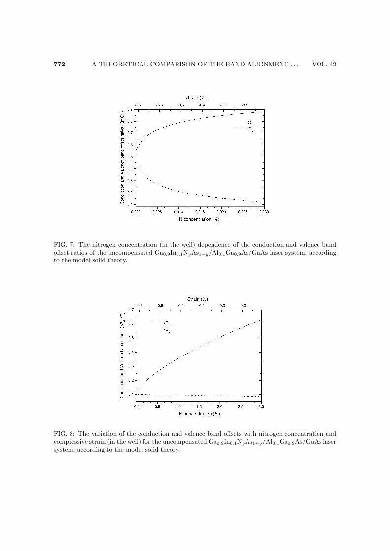
The third type of device is N-based lasers with compressively strainedGa0.9In0.1NyAs1−y quantum wells between Al0.1Ga0.9As barriers and GaAs cladding layers.Fig. 7 presents the band offset ratios for uncompensated N system with AlGaAs barriers, bymeans of the model solid theory. The addition of N to InGaAs causes substantial changesin the band alignments: adding N to InGaAs increases the CB offset and decreases theVB offset. The usual ∆Ec/∆Ev ratio changes from 1.2 to around 7 with an addition of3% nitrogen. At first a rapid and then a gradual change in band offsets have been cal-culated. The corresponding band offsets are shown in Fig. 8, which illustrates the factthat the addition of nitrogen into InGaAs certainly leads to the N-system having a bandalignment of that of the ideal case (deep C wells and shallow V wells). On the other hand,the addition of nitrogen deteriorates the laser parameters, so one should keep the N com-position low, and low N leads to high strains. So strain compensation again can be offeredas a solution in this novel material system as well, and this can be achieved by meansof using GaAsP barriers instead of AlGaAs barriers. The well composition is held fixedat Ga0.9In0.1N0.025As0.975, and the tensile strain in the barrier is varied from 0 to 0.7 %,see Fig. 9. The uncompensated system corresponds to zero strain in the barrier. First, itshould be noted from the variations of Fig. 9 that using GaAsP barriers instead of AlGaAsbarriers improves the band alignment, even in the uncompensated value. Second, the Qc
value is much higher than the Qv for the uncompensated value, and the compensation de-creases the Qc and increases the Qv value. Therefore the compensation can be thought to

VOL. 42 B. GONUL, F. KOCAK, et al. 771
FIG. 6: The calculated variation of the the conduction and valence band offsets with alu-minum concentration and tensile strain (in the barrier) for the compensated Al0.175Ga0.095In0.73As/AlyGaxIn1−x−yAs/InP laser system, according to Harrison’s model; x=0.095.
bring disadvantages to the system. Fortunately, this is not the case. Although QC andQv shows opposite trends with compensation, both conduction- and valence-band offsetsincrease with compensation, see Fig. 10. This strange behaviour of the increase of ∆Ec
with decreasing Qc can be explained as follows: the variation of the conduction band offsetis a result of the combined effect of the varition of Qc and ∆Eg, since ∆Ec = Qc∆Eg and∆Eg is the difference of the strained bandgap of the barrier and well. The rapid increasein ∆Eg (= Egbarrier
− Egwell) with P concentration eliminates the effect of the decrease in
Qc with increasing P concentration, and, as an overall results, an increase in ∆Ec withincreasing P concentration. So compensation brings further improvements to the N systemas well.
In summary, theoretical calculations have been presented to compare the band align-ments of three typical competing laser devices emitting in the neighborhood of 1.3 µm. Ourcalculations indicate that the band alignment of the N-based system agree with the com-monly accepted tendencies and available experimental data [17], so the model solid theorycan be effectively used to investigate the band alignments of N-based lasers, where onlyexperimental data has been available to date. The investigation of the band alignments ofthe three competing laser devices indicates that Al- and N-based laser systems are superiorto that of the P-based laser system. The clear comparison of the band offset ratios showsthat the introduction of opposite strain to the barrier in N-based laser not only resultsin deep electron and hole wells but also causes the electron wells to be much deeper thanthat of the hole wells, which is essential for having good high temperature characteristics.In addition, we have also shown that the use of the GaAsP barrier instead of AlGaAsbarriers improves the band alignment even in the uncompensated value in N-based lasers.
772 A THEORETICAL COMPARISON OF THE BAND ALIGNMENT . . . VOL. 42
FIG. 7: The nitrogen concentration (in the well) dependence of the conduction and valence bandoffset ratios of the uncompensated Ga0.9In0.1NyAs1−y/Al0.1Ga0.9As/GaAs laser system, accordingto the model solid theory.
FIG. 8: The variation of the conduction and valence band offsets with nitrogen concentration andcompressive strain (in the well) for the uncompensated Ga0.9In0.1NyAs1−y/Al0.1Ga0.9As/GaAs lasersystem, according to the model solid theory.

VOL. 42 B. GONUL, F. KOCAK, et al. 773
FIG. 9: The variation of the conduction and valence band offset ratios with phosphorus concentrationand tensile strain (in the barrier) for the compensated Ga0.9In0.1N0.025As0.975/Ga1−yAsPy/GaAslaser system, according to the model solid theory.
FIG. 10: The calculated variation of the the conduction and valence band offsets with phospho-rus concentration and tensile strain (in the barrier) for the compensated Ga0.9In0.1N0.025As0.975/Ga1−yAsPy/GaAs laser system, according to the model solid theory.

774 A THEORETICAL COMPARISON OF THE BAND ALIGNMENT . . . VOL. 42
Therefore, these calculations illuminate the intrinsic superiority of N-based lasers and offerthe strain-compensated N-based laser system as an ideal candidate for high temperatureoperation.
References
[1] M. S. Hybertsen, Appl. Phys. Lett. 58, 1759 (1991).[2] R. F. Kazarinov and H. R. Pinto, IEEE J. Quantum Electron. 30, 49 (1994).[3] A. F. Phillips, S. J. Sweeney, A. R. Adams, and P. J. A. Thijs, IEEE J. Sel. Top. Quantum
Electronics 5, 401 (1999).[4] S. Seki, H. Ohashi, H. Sugiura, T. Hirono, and K. Yokoyama, IEEE J. Quantum Electron. 32,
1478 (1996).[5] T. R. Chen, B. Chang, L. C. Chiu, K. L. Yu, S. Margalit, and A. Yariv, Appl. Phys. Lett. 43,
217 (1983).[6] R. F. Kazarinov and G. L. Belenky, IEEE J. Quantum Electron. 31, 423 (1995).[7] J. W. Pan and J. I. Chyi, IEEE J. Quantum Electron. 32, 2133 (1996).[8] M. Kondow, K. Uomi, A. Niva, T. Kitatani, S. Watahiki, and Y. Yazawa, Jpn. J. Appl. Phys.
35, 1273 (1996).[9] F. Hohnsdorf, J. Koch, S. Leu, W. Stolz, B. Borchert, and M. Druminski, Electron. Lett. 35,
571 (1999).[10] K. Nakahara, M. Kondow, T. Kitatani, M. C. Larson, and K. Uomi, IEEE Photon. Technol.
Lett. 10, 487 (1998).[11] S. Sato and S. Satoh, Electron. Lett. 35, 1251 (1999).[12] I. A. Buyanowa, W. M. Chen, and B. Monemar, MRS Internet J. Nitride Semicond. Res. 6, 2
(2001).[13] B. Gonul and M. Oduncuoglu Semicond. Sci. Technol. 19, 23 (2004).[14] Y. C. L. Yong, J. M. Rorison, and I. White, IEEE J. Quantum Electron. 38, 1553 (2002).[15] J. Minch, S. H. Park, T. Keating, and S. L. Chuang, IEEE J. Quantum Electron. 35, 771
(1999).[16] T. Ishikawa and J. E. Bowers, IEEE J. Quantum Electron. 30, 562 (1994).[17] W. A. Harrison, J. Vac. Sci. Technol. 14, 1016 (1977).[18] M. Hetterich, M. D. Dawson, A. Yu Egorov, D. Bernklau, and H. Riechert, Appl. Phys. Lett.
76, 1030 (2000).[19] G. Lin and C. P. Lee, Optical and Quantum Electronics 34, 1191 (2002).[20] W. Shan, W. Walukiewicz, J. W. Ager III, E. E. Haller, J. F. Geisz, D. J. Friedman, J. M.
Olson, and S. R. Kurtz, Phys. Rev. Lett. 82, 1221 (1999).[21] P. Perlin, S. G. Subramanya, D. E. Mars, J. Kruger, N. Shapiro, H. Siegle, and E. R. Weber,
Appl. Phys. Lett. 73, 3703 (1998).[22] M. Kondow, K. Uomi, A. Niva, T. Kitatani, S. Watahiki, and Y. Yazawa, Jpn. J. Appl. Phys.
Lett. 73, 3703 (1998).[23] C. Elmers, F. Hohnsdorf, J. Koch, C. Agert, S. Leu, D. Karaiskaj, and M. Hofmann, Appl.
Phys. Lett. 74, 2271 (1999).[24] H. P. Xin and C. W. Tu, Appl. Phys. Lett. 72, 2442 (1998).[25] T. L. Koch, U. Koren, R. P. Gnall, C. A. Burrus, and B. I. Miller, Electron. Lett. 26, 1431
(1988).[26] J. W. Matthews and A. E. Blakeslee, J. Cryst. Growth 24, 188 (1974).[27] A. Ghiti and U. Ekenberg, Semicond. Sci. Technol. 9, 1575 (1994).

VOL. 42 B. GONUL, F. KOCAK, et al. 775
[28] B. I. Miller, U. Koren, M.G. Young, and M. D. Chieh, Appl. Phys. Lett. 58, 1952 (1991).[29] G. Zhang and A. Ovtchinnikov, Appl. Phys. Lett. 62, 1644 (1993).[30] I. Vurgaftman, J. R. Meyer, and L. R. Ram-Mohan, J. Appl. Phys. 89, 5815 (2001).[31] J. D. Perkins, A. Mascarenhas, Y. Zhang, J. F. Geisz, D. J. Friedman, J. M. Olson, and S. R.
Kurtz, Phys. Rev. Lett. 82, 3312 (1999).[32] C. Silfvenius, B. Stalnacke, and G. Landgren, J. Cryst. Growth 170, 122 (1997).