Design of 1.9 GHz Gilbert-Cell Down-Conversion Mixer with good linearity in 0.18 µm CMOS Technology
15
Design of 1.9 GHz Gilbert-Cell Down-Conversion Mixer With good linearity in 0.18 µm CMOS Technology * K. Faitah, ** R. Mahmou * Laboratory of Electrical Engineering and Control Systems (LGECOS). Department of Electrical Engineering, National Institute of Applied Sciences (ENSA). Cadi Ayyad University, Marrakech, Morocco. Avenue Abdelkrim El Khattabi P.O box: 575 Marrakech Morocco. E-mail ([email protected]) **Laboratory Of Electrical Engineering and Control Systems (LGECOS). Department of Electrical Engineering, National Institute of Applied Sciences (ENSA). Cadi Ayyad University, Marrakech, Morocco. Avenue Abdelkrim El Khattabi P.O box: 575 Marrakech Morocco. E-mail ([email protected]) Abstract This paper describes the design of a double balanced mixer known as a Gilbert cell mixer. The proposed design, which operates at a radiofrequency (RF) of 1.9 GHz, is implemented in 0.18 μm CMOS technology at a supply voltage of 1.8 V. The components values and the size of CMOS transistors used to achieve a better linearity while keeping a good conversion gain are calculated. The obtained results show a third order input intercept point (IIP3) and an 1-dB compression point in the order of 10.5 dBm and -2 dBm, respectively when the conversion gain roughly equal to 9.12 dB. These performances justify the good linearity of the mixer compared to those using an inductive degeneration or active loads like P-channel MOS. Key words Mixer, Gilbert cell, degeneration resistor, conversion gain, linearity. 1. Introduction The CMOS technology has now reached its maturity by its very high integration degree. The choice of CMOS technology allows not only to benefit, at the present time, from the lowest price in the semiconductors market, but also from manufacturing circuits in very large quantities and in a controlled manner. The performance improvements of this technology allow to develop products operating in the 1-8 GHz frequency band for broadband applications [1][2].
-
Upload
independent -
Category
Documents
-
view
0 -
download
0
Transcript of Design of 1.9 GHz Gilbert-Cell Down-Conversion Mixer with good linearity in 0.18 µm CMOS Technology

Design of 1.9 GHz Gilbert-Cell Down-Conversion Mixer With good linearity in 0.18 µm CMOS Technology
* K. Faitah, ** R. Mahmou
* Laboratory of Electrical Engineering and Control Systems (LGECOS).
Department of Electrical Engineering, National Institute of Applied Sciences (ENSA).
Cadi Ayyad University, Marrakech, Morocco.
Avenue Abdelkrim El Khattabi P.O box: 575 Marrakech Morocco.
E-mail ([email protected])
**Laboratory Of Electrical Engineering and Control Systems (LGECOS).
Department of Electrical Engineering, National Institute of Applied Sciences (ENSA).
Cadi Ayyad University, Marrakech, Morocco.
Avenue Abdelkrim El Khattabi P.O box: 575 Marrakech Morocco.
E-mail ([email protected])
Abstract This paper describes the design of a double balanced mixer known as a Gilbert cell mixer.
The proposed design, which operates at a radiofrequency (RF) of 1.9 GHz, is implemented in
0.18 µm CMOS technology at a supply voltage of 1.8 V. The components values and the size of
CMOS transistors used to achieve a better linearity while keeping a good conversion gain are
calculated. The obtained results show a third order input intercept point (IIP3) and an 1-dB
compression point in the order of 10.5 dBm and -2 dBm, respectively when the conversion gain
roughly equal to 9.12 dB. These performances justify the good linearity of the mixer compared to
those using an inductive degeneration or active loads like P-channel MOS.
Key words Mixer, Gilbert cell, degeneration resistor, conversion gain, linearity.
1. Introduction The CMOS technology has now reached its maturity by its very high integration degree. The
choice of CMOS technology allows not only to benefit, at the present time, from the lowest price
in the semiconductors market, but also from manufacturing circuits in very large quantities and in
a controlled manner. The performance improvements of this technology allow to develop
products operating in the 1-8 GHz frequency band for broadband applications [1][2].
Despite this growth, the MOS transistor presents one of the lowest ratio current/gate width.
This has a direct influence on the transistor’s gain through its transconductance. On the other
hand, an important feature of the silicon substrate is that it is a semiconductor unlike the gallium
arsenide which is semi-insulating. This property leads losses in the substrate through parasite
capacities. So, magnetic fields introduced into the substrate may cause adverse currents. The low
substrate resistivity generates significant current contrary to very resistant substrates. Thus, there
are phenomena of interference, "cross talk" and "noise coupling", between the signals which can
be mitigated through a differential architecture, such as that adopted by the Gilbert cell,
eliminating the maximum of common mode.
The mixer is an essential block in any telecommunication system which has a critical impact
on the performances of all system functions. It is an analog multiplier, as shown in Figure 1,
which allows a time multiplication of two signals, the first one (RF signal) comes from the
receiver antenna after has been filtered and amplified, and the other signal (LO signal) comes
from a local oscillator [3].
Fig.1. RF receiver building blocks.
2. Architecture of proposed Gilbert mixer Although it has enough advantages, the single balanced mixer (SBM) is limited in terms of
linearity; its conversion gain is constant only for the weak input powers. The circuit that we will
present in Figure 2 will improve the linearity of the mixer, maintaining a low noise and a good
conversion gain. Indeed, it is composed of three differential pairs (M2, M3), (M4, M5) and
(M6, M7): each is composed of two identical transistors, all connected to a current source based of
transistor M1.
Generally, the differential pairs are intended for the acquisition of the voltages by
converting the difference of their input voltages in a current, circulating thus on a load and
converted into voltage. [4], [5].

2.1 Principle of the mixer architecture The RF pair (M2, M3) provides the gain. It consists of two common-source transistors, M2
and M3 that convert the differential input voltage in differential current. The range of differential
voltage Vid, for which the two transistors (M2, M3) are active at the same time, depends on both
the geometrical dimensions (W, L) and the generated current IG through transistor M1.
The currents I2, and I3 are then routed to two differential pairs (M4, M5) and (M6, M7)
controlled by a strong LO signal so that they operate in switching mode [6]. Such a commutation
block is the core of the circuit where RF and LO signals are mixed. Finally, the total current I0 is
converted into a voltage output IF (Vo1 - Vo2) by a load (Rload). The Figure 3 summarizes the
operating principle of this cell.
.
M4
.
M 5
I3
Vcc
I2
Rload Rload
M1
M 7
IG
M 3
.
Differential LO Input
M6
Tail current bias adjust
Io3
.
Io2
Vcc
Differential IF Output
.
Differential RF Input
Vee
.
M2
Fig.2. Gilbert cell mixer. Fig.3. Operating principle of the
Gilbert Cell.
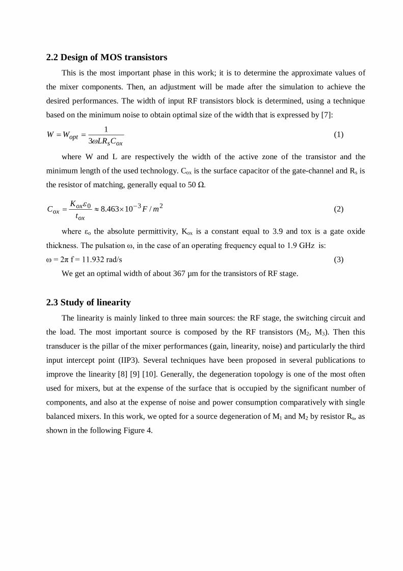
2.2 Design of MOS transistors This is the most important phase in this work; it is to determine the approximate values of
the mixer components. Then, an adjustment will be made after the simulation to achieve the
desired performances. The width of input RF transistors block is determined, using a technique
based on the minimum noise to obtain optimal size of the width that is expressed by [7]:
oxsopt CLR
WW3
1 (1)
where W and L are respectively the width of the active zone of the transistor and the
minimum length of the used technology. Cox is the surface capacitor of the gate-channel and Rs is
the resistor of matching, generally equal to 50 Ω.
230 /10463.8 mFt
KCox
oxox
(2)
where εo the absolute permittivity, Kox is a constant equal to 3.9 and tox is a gate oxide
thickness. The pulsation ω, in the case of an operating frequency equal to 1.9 GHz is:
ω = 2π f = 11.932 rad/s (3)
We get an optimal width of about 367 µm for the transistors of RF stage.
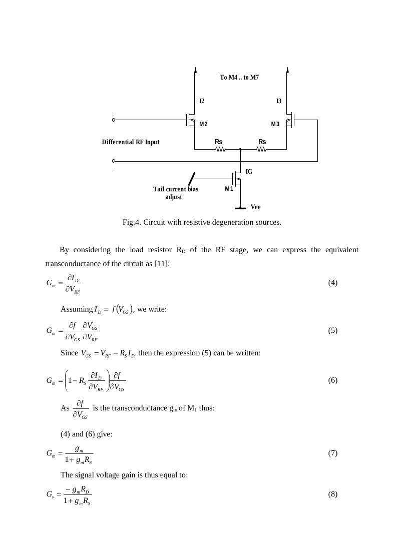
2.3 Study of linearity The linearity is mainly linked to three main sources: the RF stage, the switching circuit and
the load. The most important source is composed by the RF transistors (M2, M3). Then this
transducer is the pillar of the mixer performances (gain, linearity, noise) and particularly the third
input intercept point (IIP3). Several techniques have been proposed in several publications to
improve the linearity [8] [9] [10]. Generally, the degeneration topology is one of the most often
used for mixers, but at the expense of the surface that is occupied by the significant number of
components, and also at the expense of noise and power consumption comparatively with single
balanced mixers. In this work, we opted for a source degeneration of M1 and M2 by resistor Rs, as
shown in the following Figure 4.
Rs Rs
M 1
M 3
Tail current bias adjust
Differential RF Input
Vee
.
M2
IG.
I3I2
To M4 .. to M7
Fig.4. Circuit with resistive degeneration sources.
By considering the load resistor RD of the RF stage, we can express the equivalent
transconductance of the circuit as [11]:
RF
Dm V
IG
(4)
Assuming GSD VfI , we write:
RF
GS
GSm V
VVfG
(5)
Since DSRFGS IRVV then the expression (5) can be written:
GSRF
DSm V
fVIRG
1 (6)
As GSVf
is the transconductance gm of M1 thus:
(4) and (6) give:
Sm
mm Rg
gG
1
(7)
The signal voltage gain is thus equal to:
Sm
Dmv Rg
RgG
1
(8)
Form
s gR 1
, we have S
m RG 1
then S
RFD R
VI . We can say that the drain current is a
"linear" function of the input voltage.
This constraint will allow us, when the simulation of the circuit takes places, to correctly
calculate the values of Rs and Rload.
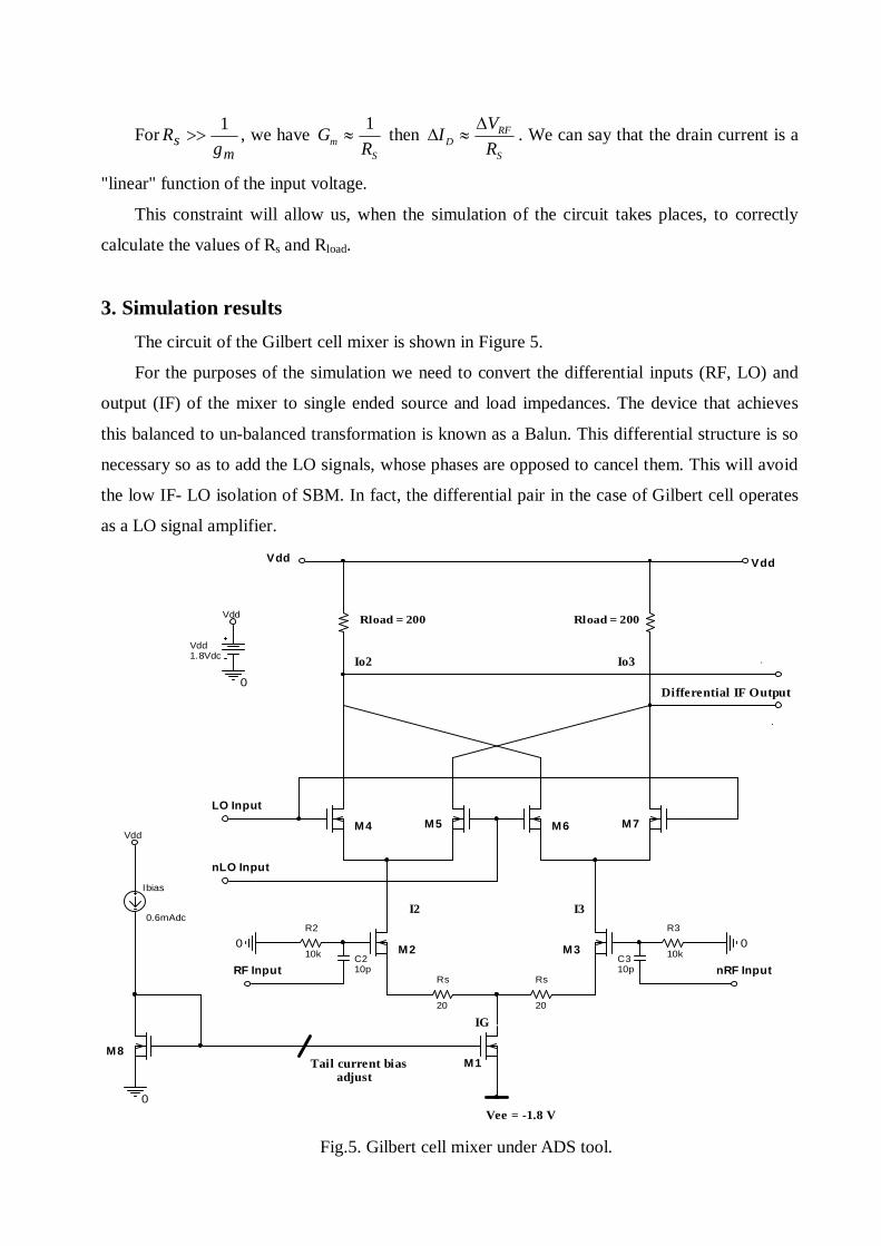
3. Simulation results The circuit of the Gilbert cell mixer is shown in Figure 5.
For the purposes of the simulation we need to convert the differential inputs (RF, LO) and
output (IF) of the mixer to single ended source and load impedances. The device that achieves
this balanced to un-balanced transformation is known as a Balun. This differential structure is so
necessary so as to add the LO signals, whose phases are opposed to cancel them. This will avoid
the low IF- LO isolation of SBM. In fact, the differential pair in the case of Gilbert cell operates
as a LO signal amplifier.
Differential IF Output
nRF Input
Ibias
0.6mAdc
Rload = 200
M8
Vdd
M1
Io2
M2
Vdd1.8Vdc
Rload = 200
Io3
R3
10k
R2
10k
nLO Input
I3
M3
LO Input
IG
C210p
Vee = -1.8 V
Vdd
C310p
M6
0
M5
Vdd
Rs
20
Vdd
Rs
20
.
I
.
0
M4
RF Input
I2
0
Tail current bias adjust
0
M7
Fig.5. Gilbert cell mixer under ADS tool.

Using the ADS tool and 0.18µm CMOS technology, the simulation was made with the
transistors size equal to W = 367 µm and L = 0.18µm, the degeneration resistor is equal to
20 and the bias current is of 0.6 mA.
The following graphs show that the proposed circuit realizes the function of mixing
frequencies.
Fig.6. Frequency input signal at 1.9 GHz. Fig.7. Frequency LO signal at 1.8 GHz.
Fig. 8 Output mixer spectrum. Fig.9. Output mixer vs time.
We note that the output shows a frequency value fRF - fLO equal to about 100 MHz.
Nevertheless a carrier at 3.7 GHz plus other unwanted harmonics are due to the non-linearity of
transistors. They can be eliminated, using a filter "to return" only the desired frequency. Being
sure that our circuit design realizes the frequency mixer function, we then simulated the most
relevant parameters to characterize the good functioning of the circuit: the conversion gain Gc,
10 ns
linearity described by the third order input intercept point (IIP3), 1-dB compression point, the 3rd
order intermodulation designated by IM3 and the power consumption.
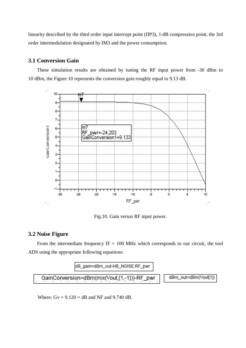
3.1 Conversion Gain These simulation results are obtained by tuning the RF input power from -30 dBm to
10 dBm, the Figure 10 represents the conversion gain roughly equal to 9.13 dB.
Fig.10. Gain versus RF input power.
3.2 Noise Figure From the intermediate frequency IF = 100 MHz which corresponds to our circuit, the tool
ADS using the appropriate following equations:
Where: Gv = 9.120 = dB and NF and 9.740 dB.
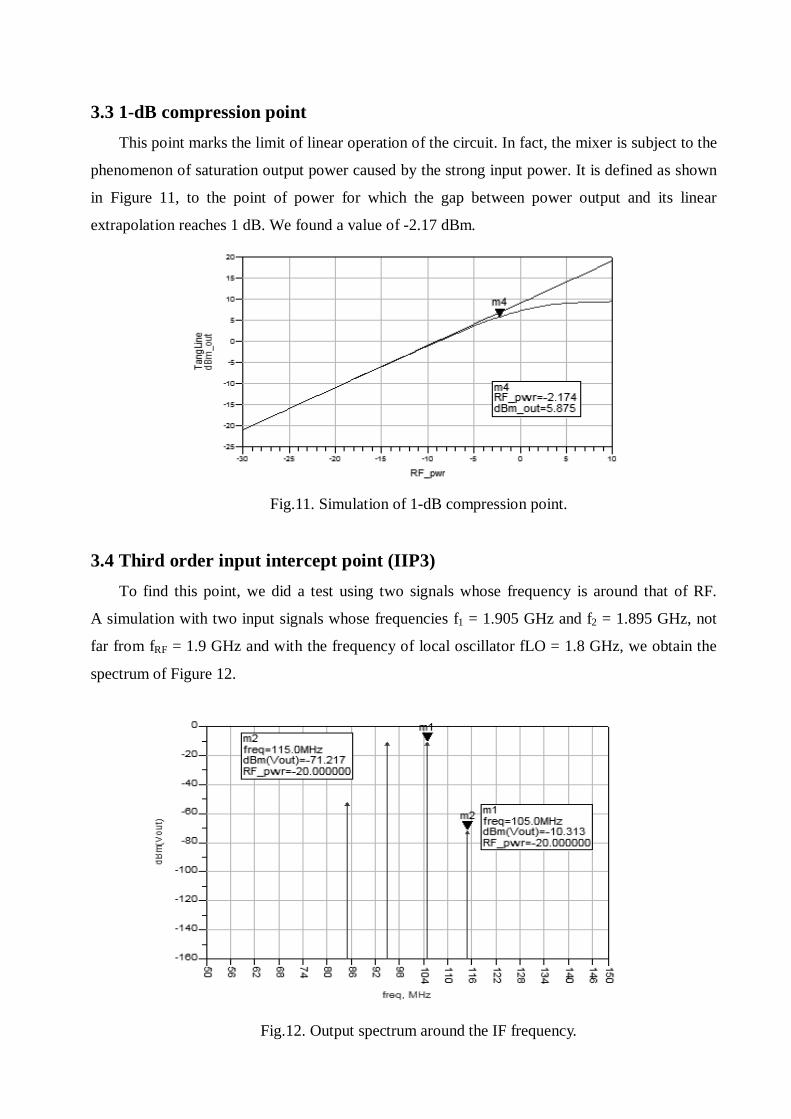
3.3 1-dB compression point This point marks the limit of linear operation of the circuit. In fact, the mixer is subject to the
phenomenon of saturation output power caused by the strong input power. It is defined as shown
in Figure 11, to the point of power for which the gap between power output and its linear
extrapolation reaches 1 dB. We found a value of -2.17 dBm.
Fig.11. Simulation of 1-dB compression point.
3.4 Third order input intercept point (IIP3) To find this point, we did a test using two signals whose frequency is around that of RF.
A simulation with two input signals whose frequencies f1 = 1.905 GHz and f2 = 1.895 GHz, not
far from fRF = 1.9 GHz and with the frequency of local oscillator fLO = 1.8 GHz, we obtain the
spectrum of Figure 12.
Fig.12. Output spectrum around the IF frequency.

By using the relationship [12]:
RFPowerIMIIP _2
33 (9)
We find the following results:
IM3 = m1 - m2
IP3_in = RF_pwr + IM3 / 2
The IM3 has a negative effect when the desired signal at the entrance of the circuit is
accompanied with two strong signals, then it will be affected by the presence of a carrier
intermodulation in the useful channel. In our case, the IM3 value of 60.9 dBm is very good, so
that this phenomenon of intermodulation hardly appears in practice. Also a positive IIP3 value
equal to 10.45 dBm justifies that this circuit can operate in linear system on a wide band powers
of entry.
3.5 Power consumption Pc
ddddc IVP (10)
Idd = 17.1 mA and Vdd = 1.8 V this gives:
Pc = 30.78 mW: power consumption is still at a reasonable level given the number of
components that make up the circuit.
4. Improvement of the conversion gain [8] To improve the conversion gain, the resistive loads of the architecture in Figure 2 must be
replaced by active loads using PMOS as shown in Figure 13.

I2
Rs
20
0
M6
M1
R3
10k
Io2
.
Rs
20
R2
10k
Vee = -1.8 V
M8
Vdd
IG
Vdd1.8Vdc
LO Input
I3
M2
M7
Io3
VddM4
P MOS1
nLO Input
M3
Ibias
0.6mAdc
0
M5
RF InputC310p
0
.
I
nRF Input
Vdd
0
Vdd
P MOS2
Differential IF Output
0
Tail current bias adjust
C210p
Fig.13. The proposed double-balanced mixer topology with p-channel MOS load.
The PMOS improves the gain, but decreases the linearity as explained in section 2.3. We
found:
-25 -20 -15 -10 -5 0 5-30 10
2
4
6
8
10
12
14
0
16
RF_pwr
Gai
nCon
vers
ion1
m7
m7RF_pwr=GainConversion1=14.401
-24.203
Fig.14. Gain versus RF input power (with PMOS load).
-25 -20 -15 -10 -5 0 5-30 10
-15
-10
-5
0
5
10
15
20
-20
25
RF_pwr
dBm
_out
m4
Tang
Line
m4RF_pwr=dBm_out=6.564
-6.812
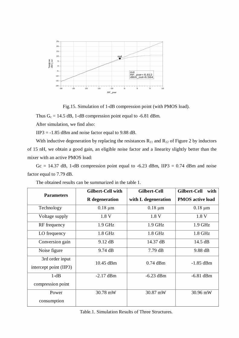
Fig.15. Simulation of 1-dB compression point (with PMOS load).
Thus Gc = 14.5 dB, 1-dB compression point equal to -6.81 dBm.
After simulation, we find also:
IIP3 = -1.85 dBm and noise factor equal to 9.88 dB.
With inductive degeneration by replacing the resistances R11 and R12 of Figure 2 by inductors
of 15 nH, we obtain a good gain, an eligible noise factor and a linearity slightly better than the
mixer with an active PMOS load:
Gc = 14.37 dB, 1-dB compression point equal to -6.23 dBm, IIP3 = 0.74 dBm and noise
factor equal to 7.79 dB.
The obtained results can be summarized in the table 1.
Parameters Gilbert-Cell with
R degeneration
Gilbert-Cell
with L degeneration
Gilbert-Cell with
PMOS active load
Technology 0.18 µm 0.18 µm 0.18 µm
Voltage supply 1.8 V 1.8 V 1.8 V
RF frequency 1.9 GHz 1.9 GHz 1.9 GHz
LO frequency 1.8 GHz 1.8 GHz 1.8 GHz
Conversion gain 9.12 dB 14.37 dB 14.5 dB
Noise figure 9.74 dB 7.79 dB 9.88 dB
3rd order input
intercept point (IIP3) 10.45 dBm 0.74 dBm -1.85 dBm
1-dB
compression point
-2.17 dBm -6.23 dBm -6.81 dBm
Power
consumption
30.78 mW 30.87 mW 30.96 mW
Table.1. Simulation Results of Three Structures.
It has shown that the proposed circuit in this study is largely better in terms of linearity
although its power consumption is quite high. But it is still acceptable.
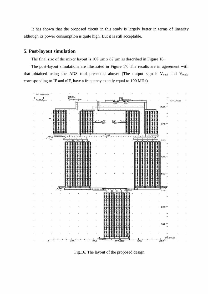
5. Post-layout simulation The final size of the mixer layout is 108 µm x 67 µm as described in Figure 16.
The post-layout simulations are illustrated in Figure 17. The results are in agreement with
that obtained using the ADS tool presented above: (The output signals Vout1 and Vout2,
corresponding to IF and nIF, have a frequency exactly equal to 100 MHz).
Fig.16. The layout of the proposed design.
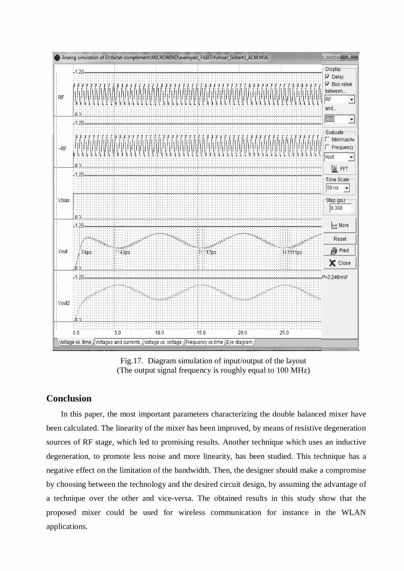
Fig.17. Diagram simulation of input/output of the layout
(The output signal frequency is roughly equal to 100 MHz)
Conclusion In this paper, the most important parameters characterizing the double balanced mixer have
been calculated. The linearity of the mixer has been improved, by means of resistive degeneration
sources of RF stage, which led to promising results. Another technique which uses an inductive
degeneration, to promote less noise and more linearity, has been studied. This technique has a
negative effect on the limitation of the bandwidth. Then, the designer should make a compromise
by choosing between the technology and the desired circuit design, by assuming the advantage of
a technique over the other and vice-versa. The obtained results in this study show that the
proposed mixer could be used for wireless communication for instance in the WLAN
applications.

Acknowledgement The authors would like to thank the professor Etienne Sicard, from LATTIS “Laboratoire
Toulousin de Technologie et d’Ingénierie des Systèmes”, Toulouse, France, for its valuable
contribution in the design of the mixer layout.
References 1. ANALOG DEVICES "Analog Devices delivers world’s first open market GSM direct
conversion radio chipset", Press Release,13th, 1999.
2. Wireless LAN Medium Access Control (MAC) and Physical Layer (PHY) specifications,
Higher speed Physical Layer Extension in the 5GHz Band, IEEE Std 802.11a-1999, Part 11.
3. K. Faitah, A. El Oualkadi, S. Belkouch, A. Ait Ouahman "Design of a modified ultra-wide
band low-noise amplifier (UWB.LNA) topology with good linearity in CMOS 65 nm
technology", Journal "Amse-Modeling", vol. 83, Issue 3,N° 3-4, 2010.
4. Etienne Sicard, Sonia Delmas Bendhia "Advanced CMOS Cell Design", Chapter 5,
pp 137-152, Edition Tata McGraw-Hill, 2007.
5. TRAN TIEN LANG "Electronique analogique des circuits integers", pp. 55-62 : Edition
Masson, Paris, 1996.
6. TERROVITIS M.T., MEYER R.G "Noise in current commuting CMOS mixers",
J.Solide-State Circuits, vol. 34, no.6, pp.772-783, June 1999.
7. LEE T.H "The Design of CMOS Radio Frequency Integrated Circuits", Cambridge University
Press, 1998.
8. Tahar Chouchane and Mohamad Sawan "A 5 GHz CMOS RF Mixer in 0.18 m CMOS
Technolohy" CCECE 2003 - CCEGEI 2003, Montreal, pp. 1905-1908, May 2003.
9. Goo-Young Jung, Jae-Hoon Shin, Tae-eoul Yun "A low noise UWB CMOS Mixer using
current bleeding and resonant inductor techniques", Wiley InterScience Journal, Volume 49,
pp. 1595-1597, April 2007.
10. K. Munusamy and Z. Yusoff "A Highly Linear CMOS Down Conversion Double Balanced
Mixer", IEEE ICSE2006 Pro. 2006, Kuala Lumpur, Malaysia, pp. 985- 989, 2006.
11. Behzad Razavi "Design of Analog CMOS Integrated CircuitsOuvrage", McGRAW-HILL
INTERNATIONAL EDITION, pp. 60-67, 2001.
12. D. Leenaerts, J. Van der Tang, Cicero S. Vaucher "Circuit Design for RF Transceivers",
KLUWER ACADEMIC PUBLISHERS, pp. 122-128, 2001.