
High-speed optical pulse transmission at 1.29-µm wavelength using low-loss single-mode fibers
10
IEEE JOURNAL OF QUANTUM ELECTRONICS, VOL. QE-14, NO. 11, NOVEMBER 1978 79 1 Special Papers High-speed Optical Pulse Transmission at 1.29-pm Wavelength Using Low-Loss Single-Mode Fibers JUN-ICHI YAMADA, MASATOSHI SARUWATARI, KOICHI ASATANI, HARUHIKO TSUCHIYA, MEMBER, IEEE, AKIO KAWANA, KOICHI SUGIYAMA, AND TATSUYA KIMURA, SENIOR MEMBER, IEEE Abstract- Optical-fiber transmission experiments in the 1.3-pm wave- length region are reported. GaInAsP/InP double-heternstructure semi- conductor laser emitting at 1.293 pm is modulated directly in nonreturn- to-zero (NU) codes at digit rates ranging from 100 Mbit/s to 1.2 Gbit/s. Itsoutput is transmitted through low-loss Ge02-doped single-mode silica fibers in 11-km lengths. Transmitted optical signals are detected by a high-speed Ge avalanche photodiode. Overall loss of the 11-km optical fibers, including 11 splices, is 15.5 dB at 1.3 Nm. Average re- ceived opticalpower levels necessary forerrorrateare -39.9 dBm at 100 Mbit/s and -29.1 dBm at 1.2 Gbit/s. In the present system con- figuration, the repeater spacing is limited by loss rather than dispersion. It seems feasible that a more than 30 km repeater spacing at 100 Mbit/s and a more than 20 km even at 1.2 Gbit/s can be realized with low-loss silica fiber cables, whose loss is less than 1 dB/km. Distinctive features and problems associated with this experimental system and constituent devices are discussed. S I. INTRODUCTION INGLE-MODE fibers can inherently transmit broadband signals over long distances with low dispersion, because only the dominant mode propagates. Bandwidthin single-mode fibers are mainly governed by material and waveguide disper- sions. It has already been pointed out that the material disper- sion of silica glass vanishesat 1.27 pm [ 11 . The wavelength to give zero total dispersion shifts to the region between 1.3 and 1.4 pm, due tothe existence of waveguide dispersion [2] , Reduction of hydro-oxy1 ions in core and cladding regions has enabled fabricating extremely low-loss fibers in this wavelength region [3]. Manuscript received April 27, 1978, revised June 20, 1978. J. I. Yamada, H. Tsuchiya, K. Sugiyama, and T. Kimura are with the Musashino Electrical Communication Laboratory, Nippon Telegraph and Telephone Public Corporation, Musashino-shi, Tokyo, Japan. M. Saruwatari and K. Asatani were with the Musashino Electrical Communication Laboratory, Nippon Telegraph and Telephone Public Corporation, Mushashino-shi, Tokyo Japan. They are now with the Yokosuka Electrical Communication Laboratory, Nippon Telegraph and Telephone Public Corporation, Yokosuka-shi, Kanagawa, Japan. A. Kawana is with the Ibaraki Electrical Communication Laboratory, Nippon Telegraph and Telephone Public Corporation, Tokai-mura, Ibaraki, Japan. Recently, continuous-wave operation of GaInAsP quaternary injection lasers has been successfully operated at the wavelength around 1.3 pm [4] . It seems feasible that the development of single-mode fibers and optical devices at the 1.3-pm wavelength region would lead to a remarkable increase in repeater spacing for large-capacity digital trunk transmission systems [2], [5], in contrast to the 0.85-pm wavelength where material and waveguide dispersions limit repeater spacing. It will be worth- while to evaluate single-mode fibers and optical devices with regard to high-speed digital transmission in t h s promising wave- length region. An 800-Mbit/s optical-fiber transmission exper- iment at 1.05 pm, reported already, shows merits of optical- fiber transmission systemsin this wavelength region [6]. This paper reports optical-fiber transmission experiments carried out at digit rate from 100 Mbit/s to 1.2 Gbit/s, using GaInAsP/InP double-heterostructure semiconductor laser emit- ting at 1.293-pm wavelength, low-loss, germanium-doped, single-mode fibers in 11-km lengths, andhigh-speed Ge ava- lanche photodiodes. These experiments are the first verifica- tion that loss and dispersion in single-mode fibers are very low atthepromisingwavelength region. Distinctive features and problems associated with the experimental system will be dis- cussed in detail. 11. OPTICAL DEVICE CHARACTERISTICS In this section, characteristics of the optical sources, detec- tor and electronic circuits used in the experimental systemare discussed in detail. A. Optical SouPce CW operation of semiconductor lasers at the 1-1.3 pm wave- length range has been reported for double-heterostructure (DH) diode lasers consisting of GaInAsPlInP [4] , GaAsSbIAlGaAsSb [7] , and GaInAs/GaInP [8]. In the present study, a GaInAsP/InP DH semiconductor laser is used as the optical source. The laser operates contin- uously at room temperature and emits at 1.293 pm [SI. Fig. 1 shows a drawing of the laser. The DH structure consists of 0018-9197/78/1100-0791$00.75 0 1978 IEEE
Transcript of High-speed optical pulse transmission at 1.29-µm wavelength using low-loss single-mode fibers
IEEE JOURNAL OF QUANTUM ELECTRONICS, VOL. QE-14, NO. 11, NOVEMBER 1978 79 1
Special Papers
High-speed Optical Pulse Transmission a t 1.29-pm Wavelength Using Low-Loss Single-Mode Fibers
JUN-ICHI YAMADA, MASATOSHI SARUWATARI, KOICHI ASATANI, HARUHIKO TSUCHIYA, MEMBER, IEEE, AKIO KAWANA, KOICHI SUGIYAMA, AND TATSUYA KIMURA, SENIOR MEMBER, IEEE
Abstract- Optical-fiber transmission experiments in the 1.3-pm wave- length region are reported. GaInAsP/InP double-heternstructure semi- conductor laser emitting at 1.293 pm is modulated directly in nonreturn- to-zero (NU) codes at digit rates ranging from 100 Mbit/s to 1.2 Gbit/s. Its output is transmitted through low-loss Ge02-doped single-mode silica fibers in 11-km lengths. Transmitted optical signals are detected by a high-speed Ge avalanche photodiode. Overall loss of the 11-km optical fibers, including 11 splices, is 15.5 dB at 1.3 Nm. Average re- ceived optical power levels necessary for error rate are -39.9 dBm at 100 Mbit/s and -29.1 dBm at 1.2 Gbit/s. In the present system con- figuration, the repeater spacing is limited by loss rather than dispersion. It seems feasible that a more than 30 km repeater spacing at 100 Mbit/s and a more than 20 km even at 1.2 Gbit/s can be realized with low-loss silica fiber cables, whose loss is less than 1 dB/km. Distinctive features and problems associated with this experimental system and constituent devices are discussed.
S I. INTRODUCTION
INGLE-MODE fibers can inherently transmit broadband signals over long distances with low dispersion, because
only the dominant mode propagates. Bandwidthin single-mode fibers are mainly governed by material and waveguide disper- sions. It has already been pointed out that the material disper- sion of silica glass vanishes at 1.27 pm [ 11 . The wavelength to give zero total dispersion shifts to the region between 1.3 and 1.4 pm, due to the existence of waveguide dispersion [2] , Reduction of hydro-oxy1 ions in core and cladding regions has enabled fabricating extremely low-loss fibers in this wavelength region [3].
Manuscript received April 27, 1978, revised June 20, 1978. J. I. Yamada, H. Tsuchiya, K. Sugiyama, and T. Kimura are with the
Musashino Electrical Communication Laboratory, Nippon Telegraph and Telephone Public Corporation, Musashino-shi, Tokyo, Japan.
M. Saruwatari and K. Asatani were with the Musashino Electrical Communication Laboratory, Nippon Telegraph and Telephone Public Corporation, Mushashino-shi, Tokyo Japan. They are now with the Yokosuka Electrical Communication Laboratory, Nippon Telegraph and Telephone Public Corporation, Yokosuka-shi, Kanagawa, Japan.
A. Kawana is with the Ibaraki Electrical Communication Laboratory, Nippon Telegraph and Telephone Public Corporation, Tokai-mura, Ibaraki, Japan.
Recently, continuous-wave operation of GaInAsP quaternary injection lasers has been successfully operated at the wavelength around 1.3 pm [4] . It seems feasible that the development of single-mode fibers and optical devices at the 1.3-pm wavelength region would lead to a remarkable increase in repeater spacing for large-capacity digital trunk transmission systems [2], [5], in contrast to the 0.85-pm wavelength where material and waveguide dispersions limit repeater spacing. It will be worth- while to evaluate single-mode fibers and optical devices with regard to high-speed digital transmission in t h s promising wave- length region. An 800-Mbit/s optical-fiber transmission exper- iment at 1.05 pm, reported already, shows merits of optical- fiber transmission systems in this wavelength region [ 6 ] .
This paper reports optical-fiber transmission experiments carried out at digit rate from 100 Mbit/s to 1.2 Gbit/s, using GaInAsP/InP double-heterostructure semiconductor laser emit- ting at 1.293-pm wavelength, low-loss, germanium-doped, single-mode fibers in 11-km lengths, and high-speed Ge ava- lanche photodiodes. These experiments are the first verifica- tion that loss and dispersion in single-mode fibers are very low at the promising wavelength region. Distinctive features and problems associated with the experimental system will be dis- cussed in detail.
11. OPTICAL DEVICE CHARACTERISTICS In this section, characteristics of the optical sources, detec-
tor and electronic circuits used in the experimental system are discussed in detail.
A. Optical SouPce CW operation of semiconductor lasers at the 1-1.3 pm wave-
length range has been reported for double-heterostructure (DH) diode lasers consisting of GaInAsPlInP [4] , GaAsSbIAlGaAsSb [7] , and GaInAs/GaInP [8].
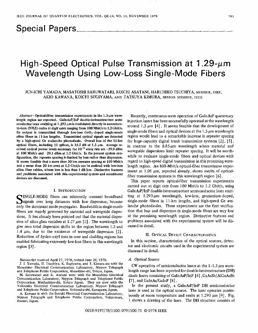
In the present study, a GaInAsP/InP DH semiconductor laser is used as the optical source. The laser operates contin- uously at room temperature and emits at 1.293 pm [SI. Fig. 1 shows a drawing of the laser. The DH structure consists of
0018-9197/78/1100-0791$00.75 0 1978 IEEE
792 IEEE JOURNAL OF QUANTUM ELECTRONICS, VOL. QE-14, NO. 11, NOVEMBER 1978
P - G ~ o I ~ I ~ ~ ~ ~ A s ~ ~ ? P o ~ ~ (lym 1 p - 1~10'9 icrn3 ( Zn )
p - 3xiO"J/cm3 ( Z n ) p - I n P ( Zprn )
G ~ o . z B ~ ~ + o & o u ( 0 5 m ) undoped
n - 3 ~ 1 0 ~ ~ 1 c r n 3 ( Te )
'\ n - 1x10¹⁸/crn3 ( S n )
n - I n P ( 3 prn )
n-lnP (substrate )
Au - Sn
Fig. 1. GaInAsP/InP DH semiconductor laser drawing.
an n-type InP confining layer (Te-doped, n = 3 X 10¹⁸/cm3), an undoped Gao.281no.72Aso.ssPo~42 active layer, a p-type InP confining layer (Zn-doped, p 2 3 X 101'/cm3), and a p-type Gao.171n0,83~o.37P0.63 cap layer (Zn-doped, p = 1 X i019/cm3) successively grown on an n-type InP substrate (Sn-doped, n = 1 X 10¹⁸/cm3). For stripe-geometry lasers, the stripe electrode is provided by depositing a 0.1-pm thick Si02 film uniformly on the GaInAsP cap layer and etching 20-pm-wide grooves in the S O 2 . Contacts were formed by evaporating Au-Cr and Au-Sn onto the p- and n-type sides, respectively. The wafer is cleaved to a 125ym length, resulting in an effective stripe con- tact area of 2.5 X 1 O-' cm2. The chip is mounted p-side down onto a diamond heat sink with In solder.
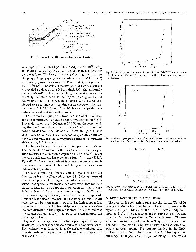
The measured output power from one side of this CW laser at room temperature is plotted against input current in Fig. 2. Threshold current Ith is 260 mA at 19.7"C and the correspond- ing threshold current density is 10.4 kA/cm2. The output power radiated from one side of the CW laser in Fig. 2 is 2 mW at 288 mA dc current. The corresponding quantum efficiency r ) is 0.72 percent, and the corresponding differential quantum efficiency qd is 7.6 percent.
The threshold current is sensitive to temperature variations. The temperature variation in threshold current under dc oper- ation measured around room temperature is 5.5 mA/"C. When the variation is expressed inexponential form,I,h a exp (T/To), To is 47 K. Since the threshold is sensitive to temperature, it is necessary to control the heat sink temperature in order to obtain stable operation.
The laser output was directly coupled into a single-mode fiber through a plane fiber end surface. Fig. 3 shows measured fiber input power plotted against input dc current. It is ob- served that spurious transverse-mode oscillation does not take place, at least up to 150 pW input power in this fiber. Very little incoherent light is coupled into the single-mode fiber due to the low coupling efficiency for the incoherent component. Coupling loss between the laser and the fiber is about 11.5 dB when the gap between them is 10 pm. The high coupling loss seems to be caused by the laser stripe width being larger than the core diameter in the single-mode fiber. It is expected that the application of narrow-stripe structures will improve the coupling efficiency.
Fig. 4 shows the spectrum of a laser operating continuously at current 1 .OS times the threshold value at room temperature. The emission was detected in a Ge avalanche photodiode. Longitudinal-mode separation is 1.8 nm and the spectrum peaks at 1.293 pm.
D C CURRENT ( r n A )
Fig. 2. Output power from one side of a GaInAsPlInP DH semiconduc- tor laser as a function of input dc current for CW room temperature operation.
6 1oc
0 3
I I I
20.5 'C
0 0 100 200 300
O C CURRENT ( r n A )
Fig. 3. Fiber input power from a GaInAsP/InP DH semiconductor laser as a function of dc current for CW room temperature operation.
Idc I Ilh = 1.05 20'C
I , , , , , , , , , I , , , , , , , , , J 1.28 1 .29 1 3
WAVELENGTH ( pm )
Fig. 4. Emission spectrum of a GaInAsP/InP DH semiconductor laser continuously operating at drive current 1.05 times threshold value.
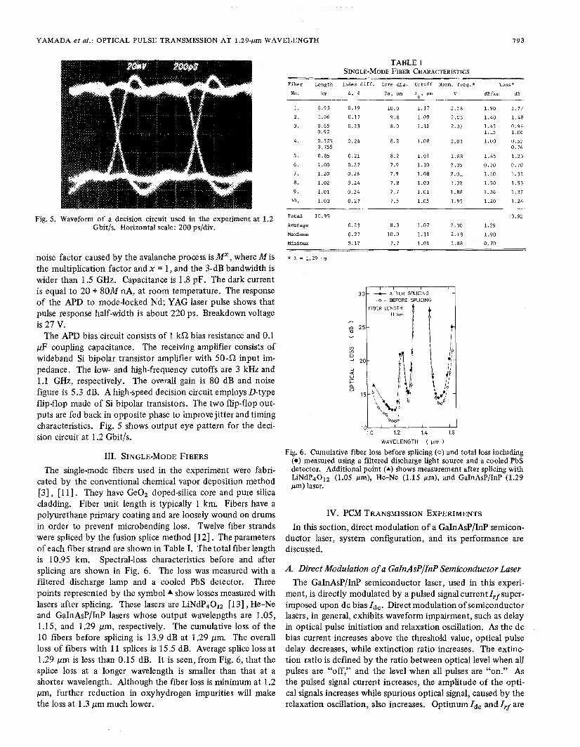
B, Optical Detector and Receiving Circuits The detector is agermanium avalanche photodiode (Ge-APD)
having a relatively high quantum efficiency in the wavelength region X > 1 pm. Details of the Ge-APD have already been reported [ 101 . The diameter of the sensitive area is 100 pm, which is 10 times larger than the fiber core diameter. The sen- sitive area surface is coated with an SiOz antireflection film. The APD is mounted in a pill-type package for use with a co- axial connector mount. The sapphire window in the diode package is not antireflection coated. The APD has a quantum efficiency of 60 percent at 1.3 pm wavelength. The excess
YAMADA et al.: OPTICAL PULSE TRANSMISSION AT 1.29-pm WAVELENGTH 193
Fig. 5. Waveform of a decision circuit used in the experiment at 1.2 Gbitls. Horizontal scale: 200 ps/div.
noise factor caused by the avalanche process is Mx, where M is the multiplication factor and x = 1, and the 3-dB bandwidth is wider than 1.5 GHz. Capacitance is 1.8 pF. The dark current is equal to 20 + 80M nA, at room temperature. The response of the APD to mode-locked Nd; YAG laser pulse shows that pulse response half-width is about 220 ps. Breakdown voltage is 27 V.
The APD bias circuit consists of 1 kC2 bias resistance and 0.1 pF coupling capacitance. The receiving amplifier consists of wideband Si bipolar transistor amplifier with 50-C2 input im- pedance. The low- and high-frequency cutoffs are 3 kHz and 1.1 GHz, respectively. The overall gain is 80 dB and noise figure is 5.3 dB. A high-speed decision circuit employs D-type flip-flop made of Si bipolar transistors. The two flip-flop out- puts are fed back in opposite phase to improve jitter and timing characteristics. Fig. 5 shows output eye pattern for the deci- sion circuit at 1.2 Gbit/s.
111. SINGLE-MODE FIBERS The single-mode fibers used in the experiment were fabri-
cated by the conventional chemical vapor deposition method [3] , [ l l ] . They have Ge02 doped-silica core and pure silica cladding. Fiber unit length is typically 1 km. Fibers have a polyurethane primary coating and are loosely wound on drums in order to prevent microbending loss. Twelve fiber strands were spliced by the fusion splice method [12] . The parameters of each fiber strand are shown in Table I. The total fiber length is 10.95 km. Spectral-loss characteristics before and after splicing are shown in Fig. 6. The loss was measured with a filtered discharge lamp and a cooled PbS detector. Three points represented by the symbol A show losses measured with lasers after splicing. These lasers are LiNdP4OI2 [13], He-Ne and GaInAsP/InP lasers whose output wavelengths are 1.05, 1.15, and 1.29 pm, respectively. The cumulative loss of the 10 fibers before splicing is 13.9 dB at 1.29 pm. The overall loss of fibers with 11 splices is 15.5 dB. Average splice loss at 1.29 pm is less than 0.15 dB. It is seen, from Fig. 6 , that the splice loss at a longer wavelength is smaller than that at a shorter wavelength. Although the fiber loss is minimum at 1.2 pm, further reduction in oxyhydrogen impurities will make the loss at 1.3 Mm much lower.
TABLE I SINGLE-MODE FIBER CHARACTERISTICS
Fiber Length Index diff. Core d i a . Cutoff Norm. freq.* L O S S *
No. km A , I 2a, urn h c , u m V dB/km dB
1. 0.93 0.19 10.0 1 .17 2.18 1.90 1.77
2. 1.06 0.17 9.8 1.09 2.03 1.40 1.48
3. 0.65 0.23 8.0 1.11 2.07 1.45 0 .94 1.15 1.06
4 . 0.525 0.24 8.2 1.08 2.01 1.00 0.52 0.755 0.76
5. 0.85 0.21 8.2 1.01 1.88 1.45 1.23
6. 1.00 0.27 7.9 1.10 2.05 0.70 0.70
7. 1 .20 0.26 7.9 1.08 2.01 1.10 1.32
8. 1.02 0.24 7.8 1.03 1.92 1.50 1.53
9. 1.01 0.24 7.7 1.01 1.88 1.36 1.37
10. 1.03 0.27 7.5 1.05 1.95 1.20 1.24
0.92
Total 10.95
Average 0.23 8.3 1.07 2.00 1.29
Maximum 0.27 10.0 1.11 2.18 1.90
Minimum 0.17 7.7 1.01 1.88 0.70
13.92
* A = 1.29 urn
301 --C AFTER SPLICING , , S I /
-a- BEFORE SPLICING 'i
10- 10 1 2 14 1.6
WAVELENGTH ( urn )
Fig. 6. Cumulative fiber loss before splicing ( 0 ) and total loss including ( 0 ) measured using a filtered discharge light source and a cooled PbS detector. Additional point (A) shows measurement after splicing with LiNdP4012 (1.05 pm), He-Ne (1.15 pm), and GaInAsP/InP (1.29 pm) laser.
IV. PCM TRANSMISSION EXPERIMENTS In this section, direct modulation of a GaInAsP/InP semicon-
ductor laser, system configuration, and its performance are discussed.
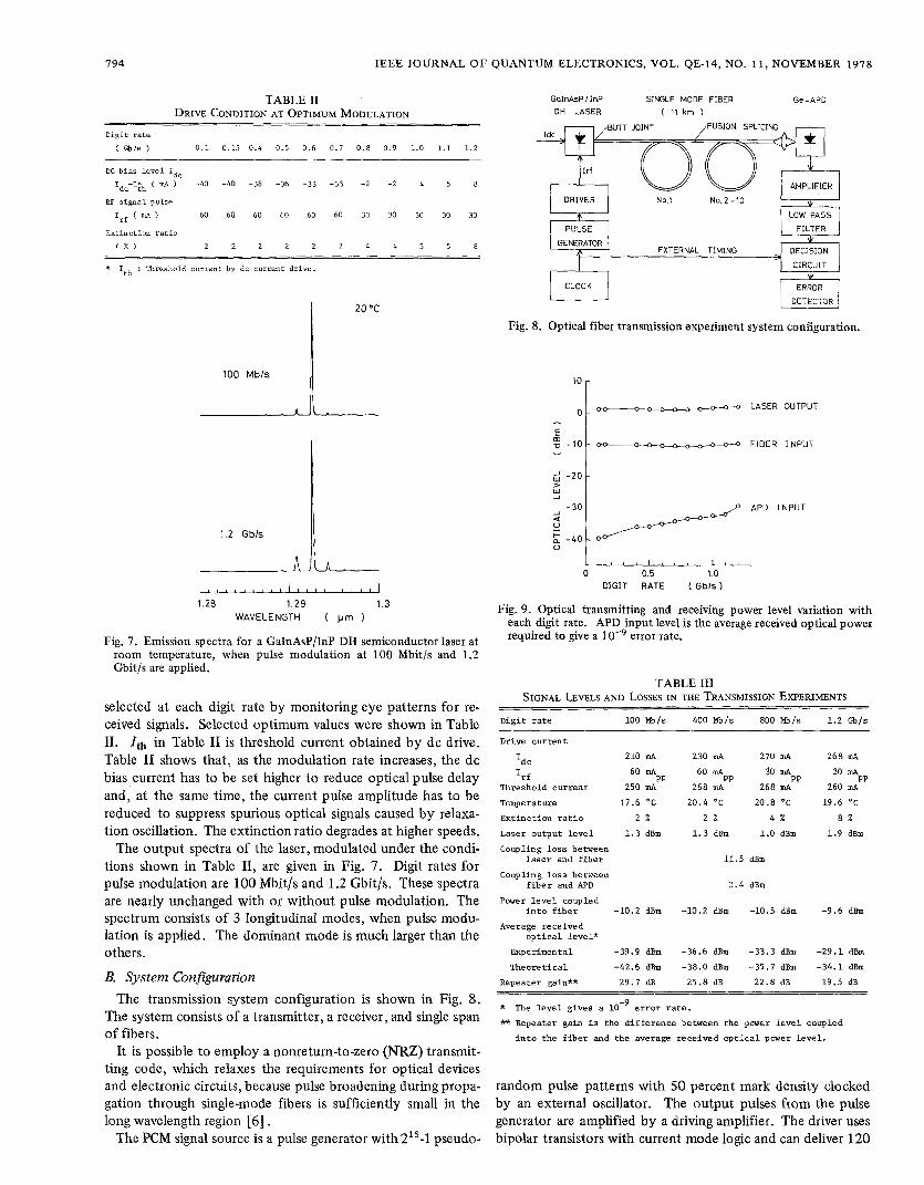
A. Direct Modulation of a GaInAsPllnp Semiconductor Laser The GaInAsP/InP semiconductor laser, used in this experi-
ment, is directly modulated by a pulsed signalcurrentIrfsuper- imposed upon dc bias I d c . Direct modulation of semiconductor lasers, in general, exhibits waveform impairment, such as delay in optical pulse initiation and relaxation oscillation. As the dc bias current increases above the threshold value, optical pulse delay decreases, while extinction ratio increases. The extinc- tion ratio is defined by the ratio between optical level when all pulses are and the level when all pulses are As the pulsed signal current increases, the amplitude of the opti- cal signals increases while spurious optical signal, caused by the relaxation oscillation, also increases. Optimum I d , and Irf are
194 IEEE JOURNAL OF QUANTUM ELECTRONICS, VOL. QE-14, NO. 11, NOVEMBER 1978
TABLE I1 DRIVE CONDITION AT OPTIMUM MODULATION
Dig i t ra te
( G b l s ) 0.1 0.15 0.4 0.5 0.6 0.7 0.8 0.9 1.0 1.1 1 . 2
DC bias level Idc
IdcI&, ( ) -40 -40 -38 -36 -33 -33 -2 -2 4 5 8
RF signal pulse
IrE ( mA ) 60 60 60 60 60 60 30 30 30 30 30
Extinction r a t i o
( % ) 2 2 2 2 2 2 4 4 5 5 8
* Ith : Threshold current by dc cmrent dr ive .
Fig. 8.
GoInAsP I InP SINGLE MODE FIBER DH LASER
Ge-APD ( 11 km )
AMPLIFIER
DRIVER No.1 No. 2 -10
4 PULSE
GENERATOR EXTERNAL TIMING
FILTER
DECISION
Optical fiber transmission experiment system configuration.
I l l l l l l ' l l l l l l l j l l l I I 1.28 1.29 1.3
WAVELENGTH ( pm )
Fig. 7. Emission spectra for a GaInAsPlInP DH semiconductor laser at room temperature, when pulse modulation at 100 Mbit/s and 1.2 Gbit/s are applied.
selected at each digit rate by monitoring eye patterns for re- ceived signals. Selected optimum values were shown in Table 11. Ith in Table I1 is threshold current obtained by dc drive. Table I1 shows that, as the modulation rate increases, the dc bias current has to be set higher to reduce optical pulse delay and, at the same time, the current pulse amplitude has to be reduced to suppress spurious optical signals caused by relaxa- tion oscillation. The extinction ratio degrades at higher speeds.
The output spectra of the laser, modulated under the condi- tions shown in Table 11, are given in Fig. 7. Digit rates for pulse modulation are 100 Mbit/s and 1.2 Gbit/s. These spectra are nearly unchanged with or without pulse modulation. The spectrum consists of 3 longitudinal modes, when pulse modu- lation is applied. The dominant mode is much larger than the others.
B. System Configuration The transmission system configuration is shown in Fig. 8.
The system consists of a transmitter, a receiver, and single span of fibers.
It is possible to employ a nonreturn-to-zero ( N U ) transmit- ting code, which relaxes the requirements for optical devices and electronic circuits, because pulse broadening during propa- gation through single-mode fibers is sufficiently small in the long wavelength region [ 6 ] .
The PCM signal source is a pulse generator with2I5-1 pseudo-
10
LASER OUTPUl
E m 73 -10 F IBER INPUT
APD INPUT
Fig. 9. Optical transmitting and receiving power level variation with each digit rate. APD input level is the average received optical power required to give a lo-' error rate.
TABLE 111 SIGNAL LEVELS AND LOSSES IN THE TRANSMISSION EXPERIMENTS
D i g i t rate 100 Mbls 400 Mb/s 800 Mb/s 1.2 Gb/s
Drive current
Id c I r f
210 mA
60 mA
Threshold current 250 "' Temperature 17.6 'C Extinction ratio 2 %
Laser output l e v e l 1 . 3 dBm
Coupling loss between
PP
laser and fiber
Coupling l o s s between f iber and APD
Power l e v e l coupled i n t o fiber -10.2 dBm
Average received opt ica l l eve l*
Experimental -39.9 dBm
Theoretical -42.6 dBm
Repeater gain** 29.7 dB
230 mA 270 mA
6o *PP "'PP 268 mA 268 mA
20.4 20.8 'C
2 % 4 % 1.3 dBm 1.0 dBm
11.5 dBm
0.4 dBm
-10.2 dBm -10.5 dBm
-36.6 dBm -33.3 dBm
-38.0 dBm -35.7 dBm
25.8 dB 22.8 dB
268 mA
30 mA
260 mA
19.6 "C
PP
8 %
1.9 dBm
-9.6 dBm
-29.1 dBm
-34.1 dBm
19.5 dB
* The level gives a lo-' error rate.
** Repeater gain is the difference between the power l e v e l coupled
into the f iber and the average received optical power l e v e l .
~ ~~~
random pulse patterns with 50 percent mark density clocked by an external oscillator. The output pulses from the pulse generator are amplified by a driving amplifier. The driver uses bipolar transistors with current mode logic and can deliver 120
YAMADA et al.: OPTICAL PULSE TRANSMISSION AT 1.29-pm WAVELENGTH 795
l o - I o L 10-12 lo-" -40 - 35 - 30
AVERAGE RECEIVED OPTICAL LEVEL (darn)
(c)
AVERAGE RECEIVED OPTICAL LEVEL (dBrn)
1,-121 ' ' I ' \I ' ' I ' I ' ' \
- 35 - 30 -25 AVERAGE RECEIVED OPTICAL LEVEL (darn 1
(d)
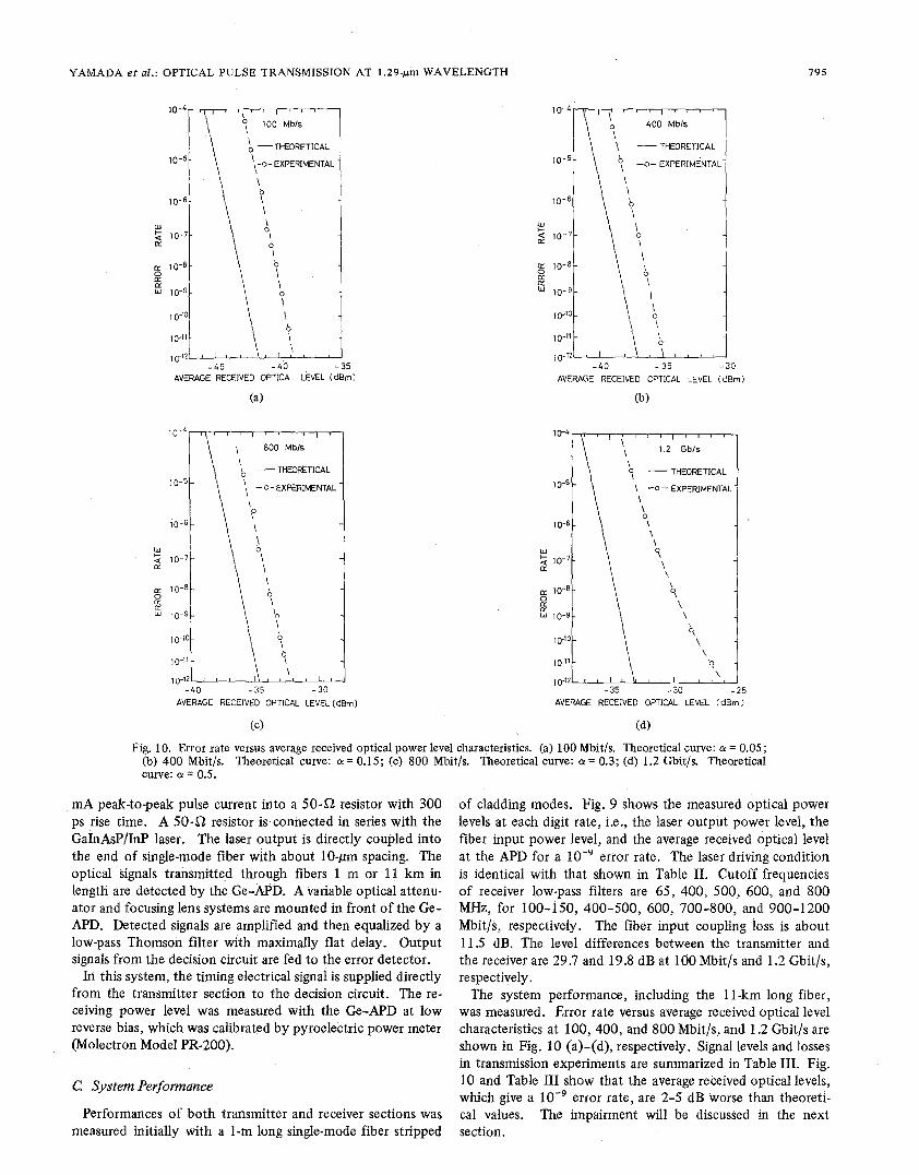
Fig. 10. Error rate versus average received optical power level characteristics. (a) 100 Mbit/s. Theoretical curve: CY = 0.05; (b) 400 Mbit/s. Theoretical curve: o( = 0.15; (c) 800 Mbit/s. Theoretical curve: a = 0.3; (d) 1.2 Gbit/s. Theoretical curve: a = 0.5.
mA peak-to-peak pulse current into a 50-i2 resistor with 300 ps rise time. A 5042 resistor is connected in series with the GaInAsP/InP laser. The laser output is directly coupled into the end of single-mode fiber with about 10-pm spacing. The optical signals transmitted through fibers 1 m or 11 km in length are detected by the Ge-APD. A variable optical attenu- ator and focusing lens systems are mounted in front of the Ge- APD. Detected signals are amplified and then equalized by a low-pass Thomson filter with maximally flat delay. Output signals from the decision circuit are fed to the error detector.
In this system, the timing electrical signal is supplied directly from the transmitter section to the decision circuit. The re- ceiving power level was measured with the Ge-AF'D at low reverse bias, which was calibrated by pyroelectric power meter (Molectron Model PR-200).
C System Perfomzance
Performances of both transmitter and receiver sections was measured initially with a 1-m long single-mode fiber stripped
of cladding modes. Fig. 9 shows the measured optical power levels at each digit rate, i.e., the laser output power level, the fiber input power level, and the average received optical level at the APD for a low9 error rate. The laser driving condition is identical with that shown in Table 11. Cutoff frequencies of receiver low-pass filters are 65 , 400, 500, 600, and 800 MHz, for 100-150, 400-500, 600, 700-800, and 900-1200 Mbit/s, respectively. The fiber input coupling loss is about 11.5 dB. The level differences between the transmitter and the receiver are 29.7 and 19.8 dB at 100 Mbit/s and 1.2 Gbit/s, respectively.
The system performance, including the 1 1-km long fiber, was measured. Error rate versus average received optical level characteristics at 100, 400, and 800 Mbit/s, and 1.2 Gbit/s are shown in Fig. 10 (a)-(d), respectively. Signal levels and losses in transmission experiments are summarized in Table 111. Fig. 10 and Table I11 show that the average received optical levels, which give a error rate, are 2-5 dB worse than theoreti- cal values. The impairment will be discussed in the next section.
796 IEEE JOURNAL OF QUANTUM ELECTRONICS, VOL. QE-14, NO. 11, NOVEMBER 1978
(b)
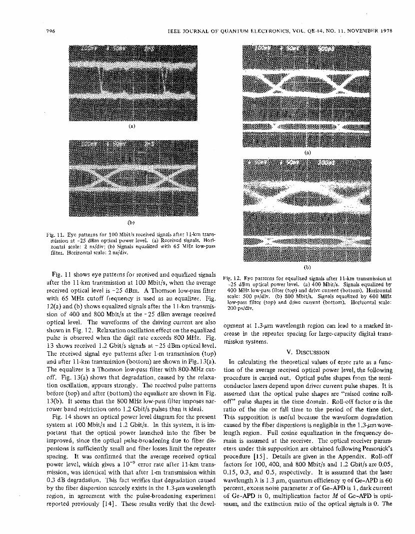
Fig. 11. Eye patterns for 100 Mbit/s received signals after 11-km trans- mission at -25 dBm optical power level. (a) Received signals. Hori- zontal scale: 2 ns/div; (b) Signals equalized with 65 MHz low-pass filter. Horizontal scale: 2 ns/div.
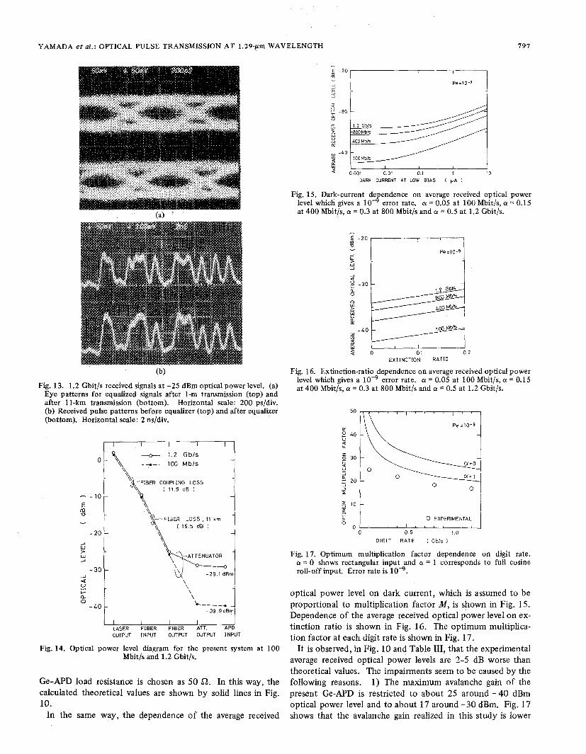
Fig. 1 I shows eye patterns for received and equalized signals after the 1 1-km transmission at 100 Mbit/s, when the average received optical level is -25 dBm. A Thomson low-pass filter with 65 MHz cutoff frequency is used as an equalizer. Fig. 12(a) and (b) shows equalized signals after the 1 I-km transmis- sion of 400 and 800 Mbit/s at the -25 dBm average received optical level. The waveforms of the driving current are also shown in Fig. 12. Relaxation oscillation effect on the equalized pulse is observed when the digit rate exceeds 800 MHz. Fig. 13 shows received 1.2 Gbit/s signals at -25 dBm optical level. The received signal eye patterns after 1-m transmission (top) and after 1 1-km transmission (bottom) are shown in Fig. 13(a). The equalizer is a Thomson low-pass filter with 800-MHz cut- off. Fig. 13(a) shows that degradation, caused by the relaxa- tion oscillation, appears strongly. The received pulse patterns before (top) and after (bottom) the equalizer are shown in Fig. 13(b). It seems that the 800 MHz low-pass filter imposes nar- rower band restriction onto 1.2 Gbit/s pulses than is ideal.
Fig. 14 shows an optical power level diagram for the present system at 100 Mbit/s and 1.2 Gbit/s. In this system, it is im- portant that the optical power launched into the fiber be improved, since the optical pulse-broadening due to fiber dis- persions is sufficiently small and fiber losses limit the repeater spacing. It was confirmed that the average received optical power level, which gives a error rate after 11-km trans- mission, was identical with that after 1-m transmission within 0.3 dB degradation. This fact verifies that degradation caused by the fiber dispersion scarcely exists in the 1.3-pm wavelength region, in agreement with the pulse-broadening experiment reported previously [ 141 . These results verify that the devel-
(b)
Fig. 12. Eye patterns for equalized signals after 11-km transmission at -25 dBm optical power level. (a) 400 Mbit/s. Signals equalized by 400 MHz low-pass filter (top) and drive current (bottom). Horizontal scale: 500 ps/div. (b) 800 Mbit/s. Signals equalized by 600 MHz low-pass filter (top) and drive current (bottom). Horizontal scale: 200 ps/div.
opment at 1.3-pm wavelength region can lead to a marked in- crease in the repeater spacing for large-capacity digital trans- mission systems.
V. DISCUSSION In calculating the theoretical values of error rate as a func-
tion of the average received optical power level, the following procedure is carried out. Optical pulse shapes from the semi- conductor lasers depend upon driver current pulse shapes. It is assumed that the optical pulse shapes are "raised cosine roll- off" pulse shapes in the time domain. Roll-off factor a is the ratio of the rise or fall time to the period of the time slot. This supposition is useful because the waveform degradation caused by the fiber dispersions is negligible in the 1.3-pm wave- length region. Full cosine equalization in the frequency do- main is assumed at the receiver. The optical receiver param- eters under this supposition are obtained following Personick's procedure [15]. Details are given in the Appendix. Roll-off factors for 100, 400, and 800 Mbit/s and 1.2 Gbit/s are 0.05, 0.15, 0.3, and 0.5, respectively. It is assumed that the laser wavelength X is 1.3 pm, quantum efficiency Q of Ge-APD is 60 percent, excess noise parameter x of Ge-APD is 1, dark current of Ge-AF'D is 0, multiplication factor M of Ge-APD is opti- mum, and the extinction ratio of the optical signals is 0. The
YAMADA e t ai.: OPTICAL PULSE TRANSMISSION AT 1.29-1.lm WAVELENGTH
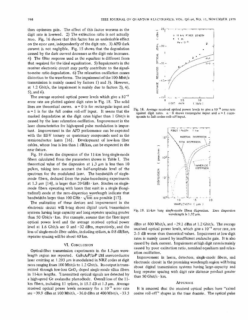
Fig. 13. 1.2 Gbit/s received signals at -25 dBm optical power level. (a) Eye patterns for equalized signals after 1-m transmission (top) and after 11-km transmission (bottom). Horizontal scale: 200 ps/div. (b) Received pulse patterns before equalizer (top) and after equalizer (bottom). Horizontal scale: 2 ns/div.
- E - 1 0 1
m,
-20 -
w J
W > J
_1
-30 - 4
I-
O
0 a
-40 -
\
I I I I I I I LASER FIBER Fl8ER ATT. APD OUTPUT INPUT OUTPUT OUTPUT I N P U l
Fig. 14. Optical power level diagram for the present system at 100 Mbit/s and 1.2 Gbit/s.
Ge-APD load resistance is chosen as 50 a. In this way, the calculated theoretical values are shown by solid lines in Fig. 10.
In the same way, the dependence of the average received
797
2 lOOMbls / -40
n
2 0001 I I
0.01 0.1 1 10 DARK CURRENT AT LOW BIAS [ p A I
Fig. 15. Dark-current de endence on average received optical power level which gives a lO-'error rate. a = 0.05 at 100 Mbit/s, a = 0.15 at 400 Mbit/s, a = 0.3 at 800 Mbit/s and a = 0.5 at 1.2 Gbitls.
EXTINCTION RATIO
Fig. 16. Extinction-ratio dependence on average received optical power level which gives a error rate. a = 0.05 at 100 Mbit/s, a = 0.15 at 400 Mbit/s, a = 0.3 at 800 Mbit/s and a = 0.5 at 1.2 Gbit/s.
50 - 1
4 1 0 1 5 [L 0
0 EXPERIMENTAL
0 ' " ~ I ' ' ' ' ~ ' ' 0 0 5 10
1 0 EXPERIMENTAL
0 0
0 0 5 10 DIGIT RATE ( Gbis )
Fig. 17. Optimum multiplication factor dependence on digit rate. a = 0 shows rectangular input and a = 1 corresponds to full cosine roll-off input. Error rate is lo*.
optical power level on dark current, which is assumed to be proportional to multiplication factor M , is shown in Fig. 15. Dependence of the average received optical power level on ex- tinction ratio is shown in Fig. 16. The optimum multiplica- tion factor at each digit rate is shown in Fig. 17.
It is observed, in Fig. 10 and Table 111, that the experimental average received optical power levels are 2-5 dB worse than theoretical values. The impairments seem to be caused by the following reasons. 1) The maximum avalanche gain of the present Ge-APD is restricted to about 25 around - 40 dBm optical power level and to about 17 around -30 dBm. Fig. 17 shows that the avalanche gain realized in this study is lower
798 IEEE JOURNAL OF QUANTUM ELECTRONICS, VOL. QE-14, NO. 1 1 , NOVEMBER 1978
than optimum gain. The effect of this factor worsens as the digit rate is lowered. 2) The extinction ratio is not actually zero. Fig. 16 shows that this factor has an undesirable effect on the error rate, independently of the digit rate. 3) APD dark current is not negligible. Fig. 15 shows that the degradation caused by the dark current decreases as the digit rate increases. 4) The filter response used as the equalizer is different from that required for the ideal equalization. 5) Impairments in the receiver electronic circuit may partly contribute to the signal- to-noise ratio degradation. 6) The relaxation oscillation causes distortion to the waveforms. The impairment of the 100-Mbit/s transmission is mainly caused by factors 1) and 3). However, at 1.2 Gbit/s, the impairment is mainly due to factors 2), 4), 5 ) , and 6).
error rate are plotted against digit rates in Fig. 18. The solid lines are theoretical curves. a = 0 is for rectangular input and a = 1 is for the full cosine roll-off input. It seems that the marked degradation at the digit rates higher than 1 Gbit/s is caused by the laser relaxation oscillation. Improvement in the laser characteristics for high-speed pulse modulation is impor- tant. Improvement in the APD performance can be expected with the 111-V ternary or quaternary compounds used as the semiconductor lasers [16] . Development of low-loss fiber cables, whose loss is less than 1 dB/km, can be expected in the near future.
Fig. 19 shows the dispersion of the 1 1-km long single-mode fibers calculated from the parameters shown in Table I. The theoretical value of the dispersion at 1.3 pm is less than 10 ps/km, taking into account the half-amplitude level of the spectrum for the modulated laser. The bandwidth of single- mode fibers, deduced from the pulse-broadening experiments at 1.3 pm [14], is larger than 20 GHz * km. Studies on single- mode fibers operating with lasers that emit in a single (longi- tudinal) mode at the zero-dispersion wavelength indicate that bandwidths larger than 100 GHz .\/kr;; are possible [17].
The realization of these devices and improvement in the electronic circuit will bring about digital trunk transmission systems having large capacity and long repeater spacing greater than 50 Gbit/s * km. For example, assume that the fiber input optical power level and the average received optical power level at 1.6 Gbit/s are 0 and -32 dBm, respectively, and the loss of single-mode fiber cables, including splices, is 0.8 dB/km, repeater spacing will be about 40 km.
The average received optical power levels which give a
VI. CONCLUSION Optical-fiber transmission experiments in the 1.3-pm wave-
length region are reported. GaInAsP/InP DH semiconductor laser emitting at 1.293 pm is modulated in NRZ codes at digit rates ranging from 100 Mbit/s to 1.2 Gbit/s. Its output is trans- mitted through low-loss Ge02- doped single-mode silica fibers in 11-km lengths. Transmitted optical signals are detected by a high-speed Ge avalanche photodiode. Overall loss of the 11- km fibers, including 11 splices, is 15.5 dB at 1.3 pm. Average received optical power levels necessary for a error rate are -39.9 dBm at 100 Mbit/s, -36.0 dBm at 400 Mbit/s, -33.3
0 I 1 km FIBER LENGTH l m
Fig. 18. Average received optical power levels to give a error rate against digit rates. CY = 0 shows rectangular input and CY = 1 corre- sponds to full cosine roll-off input.
1 ' ' ' ' I " I I FIBER LENGTH 11 km
103 - MATERIAL DISPERSION - TOTAL DISPERSION
. " : 1 0 2 - Q - z Ln 0 I
, ' / I
II I I I I I
2 0
I , , , ,
1.5 2.0 WAVELENGTH ( pm )
Fig. 19. 11-km long single-mode fibers dispersion. Zero dispersion wavelength is 1.32 pm.
dBm at 800 Mbit/s, and -29.1 dBm at 1.2 Gbit/s. The average received optical power levels, which give a error rate, are 2-5 dB worse than theoretical values. Impairment at low digit rates is mainly caused by insufficient avalanche gain. It is also caused by dark current. Impairment at high digit rates is mainly caused by poor extinction ratio, nonideal equalizers and relax- ation oscillation.
Improvement in lasers, detectors, single-mode fibers, and electronic circuit in the promising wavelength region will bring about digital transmission systems having large-capacity and long repeater spacing with digit rate distance product greater than 50 Gbit/s km.
APPENDIX It is assumed that the received optical pulses have "raised
cosine roll-off'' shapes in the time domain. The optical pulse
YAMADA e t al.: OPTICAL PULSE TRANSMISSION AT 1.29-pm WAVELENGTH 799
6 , I
I1 4[ 2
0.8 0.6 l k I I l 0 0.2 0.4 0.6 08 I
a
Fig. 20. I1 versus a for raised cosine input.
0.8 y - 1 0.6 1 I
0 0.2 0 4 0.6 0.8 1 a
Fig. 21. El versus 01 for raised cosine input.
h, (t) in the time domain is
for O < I t 1 < 2 1 - a T
1-Ct l + a for - T<Itl< 7 T
2
= 0, otherwise
where T is time slot width and CY is roll-off factor. a = 0 cor- responds to rectangular pulse and a = 1 represents full cosine roll-off pulse. Converting h, (t) into the frequency domain, we obtain, after normalization [15] ,
sin (af) * cos ( n a f ) T f { l - (2af)2}
Full cosine equalization in the frequency domain is assumed at the receiver.
Hkdf ) = 1, for O < I f 1 < 7 1 - 0
for - < I f l < - 1 + P 2 2
= 0, otherwise
and
p = 1.
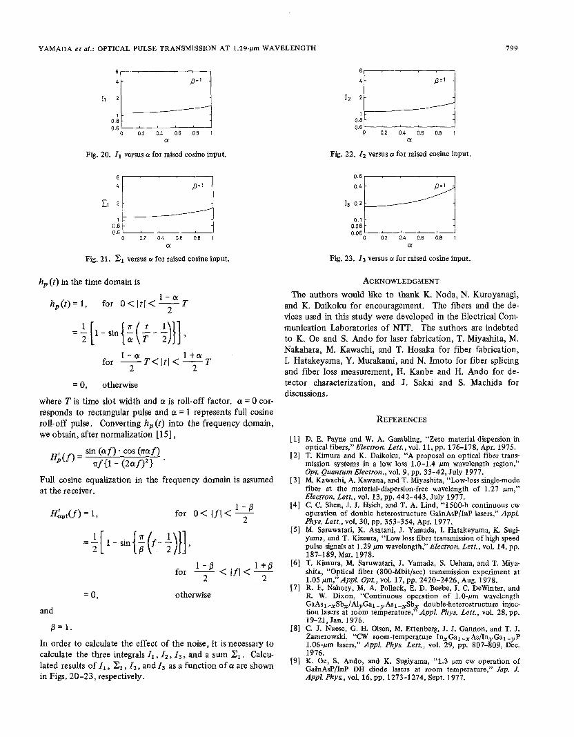
In order to calculate the effect of the noise, it is necessary to calculate the three integrals Il , 12, I3 , and a sum El . Calcu- lated results of Il , El, 12, and I3 as a function of a are shown in Figs. 20-23, respectively.
P=’ i
0.6 ’ I 0 02 0.4 0.6 0.8 1
a
Fig. 22. I2 versus Q: for raised cosine input.
0.1 1 0.0 0 0.06 I J
0 0.2 0.4 0.6 0.8 1 a
Fig. 23. I 3 versus 01 for raised cosine input.
ACKNOWLEDGMENT The authors would like to thank K. Noda, N. Kuroyanagi,
and K. Daikoku for encouragement. The fibers and the de- vices used in this study were developed in the Electrical Com- munication Laboratories of NTT. The authors are indebted to K. Oe and S . Ando for laser fabrication, T. Miyashita, M. Nakahara, M. Kawachi, and T. Hosaka for fiber fabrication, I. Hatakeyama, Y. Murakami, and N. Imoto for fiber splicing and fiber loss measurement, H. Kanbe and H. Ando for de- tector characterization, and J. Sakai and s. Machida for discussions.
REFERENCES
[ 11 D. E. Payne and W. A. Gambling, “Zero material dispersion in optical fibers,” Electron. Lett., vol. 11, pp. 176-178, Apr. 1975.
[2] T. Kimura and K. Daikoku, “A proposal on optical fiber trans- mission systems in a low loss 1.0-1.4 pm wavelength region,” Opt. Quantum Electron., vol. 9, pp. 33-42, July 1917.
[ 31 M. Kawachi, A. Kawana, and T. Miyashita, “Low-loss single-mode fiber at the material-dispersion-free wavelength of 1.27 pm,” Electron. Lett., vol. 13, pp. 442-443. July 1977.
141 C. C. Shen, J. J. Hsich, and T. A. Lind, “1500-h continuous cw operation of double heterostructure GaInAsPlInP lasers,” Appl. Phys. Lett., vol. 30, pp. 353-354, Apr. 1977.
[5] M. Saruwatari, K. Asatani, J. Yamada, I. Hatakeyama, K. Sugi- yama, and T. Kimura, “Low loss fiber transmission of high speed pulse signals at 1.29 pm wavelength,” Electron, Lett., vol. 14, pp. 187-189, Mar. 1978.
[6] T. Kimura, M. Saruwatari, J. Yamada, S . Uehara, and T. Miya- shita, “Optical fiber (800-Mbit/sec) transmission experiment a t 1.05 pm,”Appl. Opt., vol. 17, pp. 2420-2426, Aug. 1978.
[7] R. E. Nahory, M. A. Pollack, E. D. Beebe, J. C. Dewinter, and R. W. Dixon, “Continuous operation of 1.0-pm wavelength GaAsl,Sbx/AlyGal -,,As1 -$b, double-heterostructure injec- tion lasers at room temperature,” Appl. Phys. Lett., vol. 28, pp. 19-21, Jan. 1976.
[8] C. J. Nuese, G. H. Olsen, M. Ettenberg, J. J. Gannon, and T. J. Zamerowski, “CW room-temperature InxGal -,As/In Gal -,,P 1.06-pm lasers,” Appl. Phys. Lett., vol. 29, pp. 807-$09, Dec. 1976.
[9] K. Oe, S . Ando, and K. Sugiyama, “1.3 plm cw operation of GaInAsP/InP DH diode lasers at room temperature,” Jap. J. Appl. Phys., vol. 16,pp. 1273-1274, Sept. 1977.

800 IEEE JOURNAL OF QUANTUM ELECTRONICS, VOL. QE-14, NO. 1 1 , NOVEMBER 1978
[ lo] H. Ando, H. Kanbe, T. Kimura, T. Yamaoka, and T. Kaneda, “Characteristics of germanium avalanche photodiodes in wave- length region of 1-1.6 pm,” this issue, pp. 804-809.
[ l l ] J . B. MacChesney, P. B. O’Cornor, F. V. DiMarcello, J. R. Simp- son, and P. D. Lazay, in Proc. Tenth Int. Glass Congress on Glass, M. Kunugi, M. Tashiro, and N. Soga, Eds., The Ceramic Society of Japan, Tokyo, Japan, 1974, pp. 6-40.
[12] I. Hatakeyama and H. Tsuchiya, “Fusion splices for single-mode optical fibers,” IEEE J. Quantum Electron., vol. QE-14, pp. 614- 619, Aug. 1978.
[13] M. Saruwatari, T. Kimura, and K. Otsuka, “Miniaturized cw LiNdP4012 laser pumped with a semiconductor laser,’’ Appl . Phys. Lett., vol. 29, pp. 291-293, Sept. 1976.
[ 141 A. Kawana, M. Kawachi, T. Miyashita, M. Saruwatari, K. Asatani,
J. Yamada, and K. Oe, “Pulse broadening in long span single-mode fibers around material dispersion-free wavelength,” Opt. Lett., vol. 2, p. 106, Apr. 1978.
[ 151 S. D. Personick, “Receiver design for digital fiber optic communi- cation system, I and 11,” Bell Syst. Tech. J., vol. 52, pp. 843-886,
[16] T. P. Pearsall, E. Duda, M. Papuchon, and G. Roullet, “A high performance avalanche photodiode at 1.0-1.7 pm, compatible with InP/GaxInl -xAsyP1 -y integrated optics technology,” Tech. Dig. Topical Meeting o n Integrated and Guided Wave Optics, Salt Lake City, UT, Jan. 1977, Paper MC2.
[ 171 T. Kimura, M. Saruwatari, J. Yamada, S . Uehara, and T. Miyashita, “Optical fiber (800-Mbit/sec) transmission experiment at 1.05 pm,”(Appendix),Appl. Opt., vol. 17, pp. 2420-2426, Aug. 1978.
July-Aug. 1973.
High Sensitivity Optical Receivers Fiber-optic Syste
Abstract-The performance of high-speed, highquantumefficiency GaAlAsSb avalanche photodetectors suitable for a 1 .O-1.4 pm high-per- formance fiber-optical communication system is described. The incor- poration of these APD’s with state-of-the-art GaAs FET electronics can lead to hybrid integrated optical receivers with 10-20 times better sensitivity at a 100-MHz bandwidth than is available with germanium APD’s.
T HE DEVELOPMENT of optical fibers with very low loss and near zero dispersion [l] has paved the way for the
implementation of very high data rate optical communication systems. There are four major components that are necessary to realize a practical high-data-rate communication system: 1) a reliable high-speed source; 2) a low-loss, lowdispersion fiber; 3) a high-speed, highquantumefficiency avalanche photode- tector; and 4) very low-noise, high-speed electronics. The pur- pose of this paper is to describe recently obtained data on the performance of GaAlAsSb 111-V alloy high-speed avalanche photodetectors that operate in the 1.0-1.4 pm wavelength range, and to describe a technique to achieve a very sensitive, high-speed optical receiver by hybrid-integrating the APD with GaAs MESFET electronics. The result of the integration of the 111-V APD with GaAs electronics is an optical receiver with
Manuscript received June 2, 1978; revised July 17, 1978. This work was supported in part by the US. Air Force Avionics Laboratory, Wright Patterson Air Force Base, OH, and in part by the NASA Goddard Space Flight Center, Greenbelt, MD.
The authors are with the Saence Center, Rockwell International, Thousand Oaks, CA 91360.
a 100 MHz bandwidth that has a noise equivalent power 10- 20 times less than a Ge APD with the same electronics.
1 .O-1.4 pm AVALANCHE PHOTODECTORS The major requirements for an avalanche detector for a high-
1. High quantum efficiency; 2. High-speed impulse response with fast rise and fall times; 3. Uniform high-speed avalanche gain; 4. Low dark current. 111-V alloy semiconductors are superior to Ge devices because
their bandgap can be tailored to the desired wavelength, result- ing in lower dark currents than is possible with the narrow bandgap (0.66 eV) of Ge. Also, heterojunction structures that reduce surface recombination and enhance high-speed opera- tion are not possible for Ge APD’s. Spatially uniform avalanche gain is required for high-performance APD’s, which implies the necessity for uniform electric fields in uniformly multiplying (defect free) material. Not surprisingly, then, lattice disloca- tions due to lattice mismatch at heterojunction interfaces would preclude the attainment of uniformly high gains in lattice mis- matched heterojunction APD’s. There are two 111-V alloy sys- tems that can be lattice matched over the 1.0-1.4 pm wave- length range: GaAlAsSb grown on GaSb and InGaAsP grown on InP. We have fabricated APD’s of both types. For reasons to be discussed later, our GaAlAsSb heterojunction APD’s have shown the best high-speed performance.
The avalanche photodiodes were fabricated from double heterostructure layers grown by liquid phase epitaxy in the
speed, high-sensitivity fiber optical receiver are:
0018-9197/78/1100-0800$00.75 0 1978 IEEE