Drain Current Noise Spectrum Measurement in 0.18 µm ...
84
Drain Current Noise Spectrum Measurement in 0.18 μm MOSFET Using Integrated SiGe HBT Low-Noise Transimpedance Amplifier by Jingshan Wang A thesis submitted to the Graduate Faculty of Auburn University in partial fulfillment of the requirements for the Degree of Master of Science Auburn, Alabama August 3, 2013 Keywords: Drain Current Noise, Thermal Noise, 1/f noise, Corner Frequency, TIA, S-Parameter Copyright 2013 by Jingshan Wang Approved by Guofu Niu, Chair, Alumni Professor of Electrical and Computer Engineering Fa Foster Dai, Professor of Electrical and Computer Engineering Bogdan Wilamowski, Professor of Electrical and Computer Engineering
-
Upload
khangminh22 -
Category
Documents
-
view
1 -
download
0
Transcript of Drain Current Noise Spectrum Measurement in 0.18 µm ...

Drain Current Noise Spectrum Measurement in 0.18 µm MOSFET Using Integrated SiGe
HBT Low-Noise Transimpedance Amplifier
by
Jingshan Wang
A thesis submitted to the Graduate Faculty of
Auburn University
in partial fulfillment of the
requirements for the Degree of
Master of Science
Auburn, Alabama
August 3, 2013
Keywords: Drain Current Noise, Thermal Noise, 1/f noise, Corner Frequency, TIA, S-Parameter
Copyright 2013 by Jingshan Wang
Approved by
Guofu Niu, Chair, Alumni Professor of Electrical and Computer Engineering
Fa Foster Dai, Professor of Electrical and Computer Engineering
Bogdan Wilamowski, Professor of Electrical and Computer Engineering

ii
Abstract
We measured drain current noise power spectral density (PSD) in 0.18 µm metal oxide
semiconductor field effect transistor (MOSFET) using integrated Silicon-Germanium (SiGe)
Heterojunction Bipolar Transistor (HBT) low-noise transimpedance amplifier (TIA). This
measurement system extends the noise-measuring capabilities beyond 2.5 GHz to detect the
white noise component beyond the 1/f noise corner frequency. In this work, the corner frequency
is approximately 2 GHz, which comes from radio frequency (RF) thermal noise measurement
directly instead of the extension line of 1/f noise at low frequencies. PSD of drain current
thermal noise is in the range from 1 22-10 A2/Hz to 5 22-10 A
2/Hz for drain current from 1mA
to 12 mA. S-parameters are measured to calculate the gain of device under test (DUT) and TIA
system.

iii
Acknowledgments
First of all, I would like to express my deepest gratitude to my faculty advisor Dr. Guofu
Niu for his technical and moral support throughout my Master’s program, without which this
thesis would not have been possible. His vast knowledge and valuable feedback greatly
contribute to the work. His patience and constant encouragement strengthened me during my
whole graduate study.
Several people deserve special recognition for their contributions to my thesis. I would
like thank Dr. Bogdan Wilamowski and Dr. Fa Dai for serving on my committee and all the help
throughout my graduate study. This work would not have materialized without Dr. Fa Dai’s
support of measurement equipment. Also, I am very grateful to Dr. Stewart Taylor and Dr.
Xiaoyun Wei for sharing their TIA design.
Many thanks also go to Dr. Stuart Wentworth and Dr. Lloyd Riggs. Their
recommendation and encouragement help me gain both the opportunity to continue my academic
research and the confidence to face new challenge in the future.
Besides, I would like to thank my group mates Hongyun Xie, Lan Luo, Ziyan Xu, Zhen
Li, Ruocan Wang and Xiaojia Jia. The time on and off working with them was pleasant and
memorable.
Finally, I would like to thank my family, my mother, my brother, my sister in law, my
parents in law and my husband Qiang Gu, for their selfless support and love, without them, I
iv
would not have begun my Master’s program. Most importantly, I need to thank God for the most
precious gift I ever have, Derrick, my one year old son. He helps me realize the responsibility I
have for whatever I am working on.

v
Table of Contents
Abstract ......................................................................................................................................... ii
Acknowledgments........................................................................................................................ iii
List of Figures ............................................................................................................................. vii
List of Abbreviations .................................................................................................................... x
Chapter 1 Introduction .................................................................................................................. 1
1.1 Thermal Noise ............................................................................................................ 3
1.1.1 Drain Current Thermal Noise ............................................................................ 3
1.1.2 Induced Gate Noise and Gate-Drain Correlation Noise .................................... 5
1.2 Flicker Noise (1/f Noise) ............................................................................................ 7
Chapter 2 Drain Current Noise Measurement Methods ............................................................. 10
2.1 Noise Parameters Measurement System ................................................................... 10
2.2 Noise PSD Measurement System Using Discrete TIA ............................................. 14
2.3 Noise PSD Measurement System Using Integrated TIA on Chip ............................ 16
2.3.1 Noise Measurement System in the Thesis ....................................................... 17
2.3.2 SiGe HBT TIA ................................................................................................. 28
Chapter 3 Noise Measurement and Data Analysis .................................................................... 33
3.1 Noise Measurement .................................................................................................. 33
3.2 Experimental Results Analysis ................................................................................. 37

vi
Appendix
Appendix A On-Wafer DC Measurements ................................................................................ 46
A.1 Introduction ............................................................................................................. 46
A.2 DC Measurements for Standalone MOSFET .......................................................... 48
A.2.1 IDS-VDS and IDS-VGS Measurements ................................................................ 48
A.2.2 gds and gm ....................................................................................................... 49
A.3 DC Measurements for Integrated DUT in Circuit ................................................... 51
A.3.1 Measurement Equivalent Circuit .................................................................... 51
A.3.2 IDS-VDS Measurement and gm Extraction ......................................................... 52
Appendix B On-Wafer S-Parameters Measurements ................................................................ 57
B.1 Introduction ............................................................................................................. 57
B.2 S-Parameters Measurements System ...................................................................... 60
B.3 S-Parameters Measurements for Standalone MOSFET ........................................... 63
B.4 S-Parameters Measurements for Integrated DUT and TIA System ......................... 67
Bibliography ............................................................................................................................. 72

vii
List of Figures
Figure 1.1 A typical plot of the drain current noise versus frequency in log-log axes ................. 2
Figure 1.2 Measured γ values for different technologies reported in the literature ...................... 5
Figure 1.3 Extracted channel noise, induced gate noise, correlation noise, and cross-correlation
coefficient as a function of frequencies for devices with different channel lengths ... 7
Figure 2.1 System configuration for radio frequency noise measurements................................ 11
Figure 2.2 Schematic diagram for the measurement system shown in Figure 2.1 ..................... 12
Figure 2.3 Block diagram of the noise PSD measurement setup ................................................ 14
Figure 2.4 A typical equivalent input noise VSD ....................................................................... 15
Figure 2.5 Noise measurement system using integrated TIA on chip ........................................ 17
Figure 2.6 A sample noise power measured result ..................................................................... 17
Figure 2.7 Noise measurement system using SiGe TIA on chip ................................................ 18
Figure 2.8 Die photo with DUT and TIA on chip....................................................................... 19
Figure 2.9 Simple equivalent circuit for noise from Rg,bias ......................................................... 20
Figure 2.10 A typical output power of amplified noise .............................................................. 21
Figure 2.11 A typical output power spectral density of output power........................................ 22
Figure 2.12 A typical output VSD .............................................................................................. 23
Figure 2.13 Noise measurement system equivalent circuit ........................................................ 24
Figure 2.14 Equivalent two ports network .................................................................................. 24
Figure 2.15 A typical noiseinV , vs frequency .................................................................................. 26

viii
Figure 2.16 A typical Sid vs frequency ....................................................................................... 27
Figure 2.17 Noise factor ץ versus frequency .............................................................................. 27
Figure 2.18 A typical output PSD of NMOS + TIA system, TIA noise floor and SA noise floor
versus frequency ..................................................................................................... 29
Figure 2.19 Power spectral density of output power with/without TIA noise effect .................. 30
Figure 2.20 Measured I-V curve of TIA with DUT biased off ................................................... 31
Figure 2.21 A typical totalZ vs frequency ................................................................................... 31
Figure 2.22 A typical Stia and Sid vs frequency. .......................................................................... 32
Figure 3.1a Drain current noise measurement system setup ....................................................... 34
Figure 3.1b Drain current noise measurement system diagram .................................................. 34
Figure 3.2 Block diagram of operation theory for spectrum analyzer ........................................ 35
Figure 3.3 Die photo with right AC probe and DC probes on pads............................................ 36
Figure 3.4 Configuration of Eye-Pass DC probes (Cascade Microtech Company) ................... 37
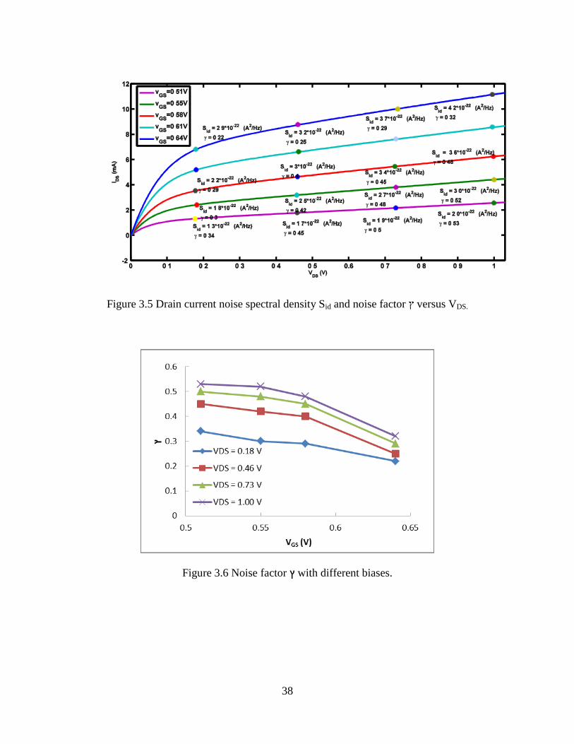
Figure 3.5 Drain current noise spectral density Sid and noise factor ץ versus VDS ..................... 38
Figure 3.6 Noise factor ץ with different biases ........................................................................... 38
Figure 3.7 Extracted noise factor ץ vs VGS in 0.18 µm technology ............................................ 39
Figure 3.8 Drain current noise PSD Sid vs Vgs ........................................................................... 39
Figure 3.9 Drain current noise PSD Sid vs Vgs in 0.18 µm technology ....................................... 40
Figure 3.10 Drain current noise PSD Sid vs drain current IDS .................................................... 40
Figure 3.11 Drain current noise PSD Sid vs drain current IDS in 90 nm technology ................... 41
Figure 3.12 Comparison of output noise power ........................................................................ 42
Figure 3.13 Comparison of Sid .................................................................................................... 43
Figure 3.14 Comparison of 43 ...................................................................................................... ץ
Figure 3.15 Sid vs frequency at fixed VGS ................................................................................... 44

ix
Figure 3.16 Sid vs frequency at fixed VDS ................................................................................... 45

x
List of Abbreviations
SiGe Silicon-Germanium
HBT Heterojunction Bipolar Transistor
TIA Transimpedance Amplifier
DUT Device Under Test
MOSFET Metal–Oxide–Semiconductor Field-Effect Transistor
NMOS N-Type Channel Metal–Oxide–Semiconductor
PSD Power Spectral Density
RF Radio Frequency
LNA Low Noise Amplifier
SA Spectrum Analyzer
VSD Voltage Spectral Density
NF Noise Figure

1
Chapter 1
Introduction
All semiconductor devices generate noise that can interfere with weak signals when used
in circuits. Therefore, it is important to find ways to measure noise. There are several types of
fundamental noise present in semiconductor device: thermal noise, flicker noise also called 1/f
noise, shot noise, generation-recombination noise and burst noise. These noises vary with device
structure and operating conditions. Thermal noise and flicker noise are two major types of noise
in metal oxide semiconductor field effect transistor (MOSFET). The purpose of Chapter 1 is to
introduce these different types of noise, especially the thermal noise in MOSFET.
A typical drain current noise PSD versus frequency plot is shown in Figure
1.1.Theoretically, a plot of drain current noise power-spectral density versus frequency in log-log
axes is a straight line with the slope of approximately 1/f at low frequency and a horizontal line
at high frequency. There is a corner at the intersection of these two lines which is valued from
several hertz to several gigahertz depending on device geometry, construction, and bias. With the
development of semiconductor technology, the corner frequency becomes higher and higher [1].
Usually, 1/f noise is measured using time domain equipment [2], such as dynamic signal
analyzer. Since the drain current thermal noise is too weak to be measured directly, the main
method for thermal noise measurement is based on measurement of noise parameters [3], such as
noise figure (NF). Chapter 2 gives background material for thermal noise measurement method.
The history of thermal noise measurement for MOSFET is introduced. Our noise measurement
system and basic working theory are described. The algorithm used here is specific for our test
system. The on-chip Silicon-Germanium (SiGe) Heterojunction Bipolar Transistor (HBT)

2
Transimpedance Amplifier (TIA) used to amplify drain current noise, is introduced. There are
several requirements for TIA to meet to be able to measure MOSFET drain current noise.
Chapter 3 describes the process of noise measurement and analysis of experimental result.
The power spectral density (PSD) of drain current noise Sid and thermal noise factor ץ are
extracted. We find that Sid increases with IDS at fixed VDS. It also increases with VDS at fixed VGS
as well as increases with VGS at fixed VDS. The values of noise factor ץ from our extraction are
consistent with reported values in literature for similar technologies.
Figure 1.1 A typical plot of the drain current noise versus frequency in log-log axes.
Different types of fundamental noise are present in semiconductor devices: thermal noise,
flicker noise (1/f noise), generation-recombination noise, shot noise and burst noise. Thermal
noise and shot noise are white noise. 1/f noise origin remains a mystery. Thermal noise and 1/f
noise are the two major concerns for drain current noise measurement.
With channel length scaling and the carrier mobility improvement, the cut-off frequency
of MOSFET can go up to hundreds of gigahertz [4]. Hence, MOSFET are widely used in high

3
speed radio frequency RF integrated circuits. In these circuits, drain current noise becomes a
critical issue.
1.1 Thermal Noise
Thermal noise is generated by random motion of free carriers in resistive materials. It is
present in all circuit elements containing resistance regardless of any applied voltage. In 1928,
J.B. Johnson was the first to prove that there is fluctuating movement of charges in thermal
equilibrium [5]. In an ideal resistor, thermal noise is independent of frequency. In other words,
the power spectral density is nearly constant throughout the frequency spectrum for a fixed
bandwidth.
1.1.1 Drain Current Thermal Noise
Starting from van der Ziel (1962) [6], many drain current thermal noise models are
developed. In 2002, Chen and Deen proposed their new model which considered the channel
length modulation (CLM) effect [7]. In 2005, Paasschens, Scholten & van Langevelde provided
channel thermal noise model which considered velocity saturation effect and separated the
position and voltage dependence for the channel conductance [8]. The noise factor ץ was
discussed in both [7] and [8]. This noise factor was introduced in one of the most prevalent
models for drain current noise PSD, Sid, in long channel device at strong inversion region by van
der Ziel [1]:
0id 4S dsgKT , (1.1)
where )('g 0ds TGSox
DS
DS VVL
WC
V
I
, (1.2)

4
Vd
0000
Vd
00
2
00
]/)([
]/)([
dVgVg
dVgVg , (1.3)
K is Boltzmann constant, T is absolute temperature, ץ is thermal noise factor, 0dsg is drain-
source conductance evaluated at drain-source voltage DSV = 0 V, W is channel width, L is
channel length, is channel mobility, oxC ' is oxide capacitance per unit area, GSV is gate-source
voltage and TV is threshold voltage, g(x) is the conductance per unit length, V0(x) is the channel
potential at the point, g0 is conductance at V0=0. The value of ץ is 2/3 and 1 in the saturation and
triode regions for long channel device, respectively.
With technology scaling, oxC ' is increased, is decreased while the product oxC ' is
increased [4]. If L
Wand TGS VV are fixed, both 0dsg and Sid increase with reducing the physical
size of devices. If L is fixed for a certain technology, increasing W can result in increasing Sid.
The parameter ץ as a noise factor is defined [1] from equation (1.1) as
0
id
4
S
dsKTg . (1.4)
Later, the ץ values are found higher than 2/3 in a short channel transistors working in the
saturation region [7-10]. Actually, ץ values are different with different semiconductor
technologies [10]. ץ is widely used in literatures to demonstrate the enhanced channel thermal
noise in short channel transistors as shown in Figure 1.2. The ץ range measured in our work is
from 0.22 to 0.53 at bias sets VDS from 0.18 V to 1 V and VGS from 0.51 V to 0.64 V in 0.18 µm
technology. The bias sets we used are in moderate region. The values of ץ are from 1 to 2 at bias
sets VDS from 1.5V to 1.8V and VGS from 1 to 1.8 in the same technology shown in Figure 1.2.
More comparisons are discussed in section 3.2.

5
Figure 1.2 Measured γ values for different technologies reported in the literature [10].
1.1.2 Induced Gate Noise
Random fluctuations of the potential in the channel are coupled to the gate terminal
through the oxide capacitance leading to induced potential fluctuations on the gate. Drain noise
and gate noise are correlated in MOSFET with frequency dependence.
In van der Ziel model [1], PSD of gate current noise Sig is given by:
GgKT4Sig (1.5)
where = 4/3, and the saturation gate conductance Gg is:
m
ox
Gg
WLC 22 )'(
45
4g
(1.6)

6
where gm is transconductance.
In saturation, the cross-correlation of reduced gate current noise and drain current noise is
given by [1],
KTq
WLCii ox
d 4'
i*
g (1.7)
where i is the imaginary unit. The correlation coefficient between gate and drain current
fluctuations is i0.4 [1].
The gate-to-source capacitance decreases when the channel length decreases. Hence, both
induced gate noise and its correlation with the channel thermal noise decrease [11]. The origin of
this comparatively low coefficient is induced charge profile on the gate, and it will not occur in
short channel MOSFET [12]. In 0.18 µm technology which is used in our project, PSDs of the
channel noise (drain current noise), induced gate current noise, correlation of induced gate
current noise and drain current noise, and cross-correlation coefficient are extracted [12] and
shown in Figure 1.3.

7
Figure 1.3 Channel noise, induced gate noise, correlation of these two noises, and cross-
correlation coefficient as a function of frequencies for devices with different channel lengths [12].
1.2 Flicker Noise (1/f Noise)
Unlike other noises, there are many different explanations of the origin of flicker noise or
1/f noise. There are two major models and concepts for 1/f noise [13]. The first theory describes
the origin of 1/f as the random fluctuation of the number of carriers in the channel because of the
fluctuations in the surface potential [4]. PSD of the equivalent drain noise current Sid can be
calculated by [4]
2
m2
1 g11
'S
cfWLC
K
ox
id (1.8)

8
where )('g m TGSox VVCL
W (1.9)
in saturation region. 𝐾1 is bias dependent quantity which increases with technology scaling, c is
between 0.7~1.2 for n-channel device. This model obtains 1/f noise by superposing many
different spectra of generation-recombination noise with a specific statistical distribution of [13].
Free carriers are randomly trapped and released by traps located near the silicon-oxide interface,
causing noise in drop current.
At corner frequency, thermal noise Sid from equation (1.1) equals 1/f noise Sid from
equation (1.8), so the corner frequency, cornerf , is calculated by
WLC
gK
gKTf
oxds
corner 2
2
1
0 '4
1m
(1.10)
Substituting equation (1.2) and (1.9) to (1.10), cornerf can be simplified to
KTL
Kf corner
4
)V-V(2
TG1 . (1.11)
If (VG-VT) is fixed, cornerf increases with decreasing L. With technology scaling, cornerf becomes
bigger and bigger.
The second theory attributes 1/f noise to the mobility [4]. Under this theory, PSD of the
equivalent drain noise current is given by
2GS
d
11
'
VS m
ox
i gfWLC
K )( (1.12)
where 𝐾(𝑉𝐺𝑆) is bias dependent quantity. In this model, both lattice scattering and impurity
scattering are considered. It is assumed that only scattering on the silicon lattice generates 1/f
noise. Similar to the first model, if VG and VT are fixed, cornerf increases with decreasing L.

9
In our work, DUT is a NMOS with channel width 2.3100W µm where100 is gate
finger number, and channel length L = 0.18 µm. The reported noise factor ץ for that technology
is approximately in the range from 2/3 to 2 for several bias sets in [7], [12] and [14]. The corner
frequency we measured is approximately 2 GHz.

10
Chapter 2
Drain Current Noise Measurement Methods
As mentioned in Chapter 1, the corner frequency becomes higher and higher with the
development of semiconductor technology in MOSFET. To measure thermal noise which
dominates after 1/f corner frequency, the noise measurement should be taken in very high
frequency and it is up to several gigahertz for modern semiconductor technologies. Another
difficulty is the thermal noise is too weak to be measured directly on noise measurement
equipment. The main method for thermal noise measurement is based on measurement of noise
parameters [3], F or NF. From 1986, TIA is used as a low noise amplifier (LNA) to boost the
drain current noise and improve the measurement accuracy [8]. Approximately one decade later,
TIA is integrated with DUT on chip for gallium arsenide GaAs metal-semiconductor field effect
transistor MESFET[15] to reduce the parasitic capacitance and inductance. In our project, SiGe
HBT TIA is integrated with a NMOS on chip to help with drain current noise measurement in
0.18 µm technology.
2.1 Noise-Parameters Measurement System
Different from the 1/f noise measurement, where the noise PSD can be directly measured
using a dynamic signal analyzer, the main thermal noise measurement method is measuring the
noise factor F (or noise figure NF in dB) and/or its well-known noise parameters developed by
Haus et al. in [16], to evaluate the thermal noise characteristics. In [16], F (or NF) is presented as
a mathematical equation
11
s
n2
optsminG
R|Y-Y|FNF N (2.1)
where Ys = Gs + i·Bs is the admittance of source, Yopt = Gopt + i·Bopt is optimized source
admittance, NFmin is minimum noise figure, Rn is equivalent noise resistance. This representation
is based on a noisy two-port network expended from Rothe and Dahlke in [17]. Haus et al.’s
impedance-based representation [16] demonstrates the dependence of noise factors on the source
admittances attached to the input port of the noisy two-port network. In the measurement, NF is
measured by Noise Figure Analyzer NFA for certain Ys firstly, noise parameters NFmin, Rn and
Yopt can be calculated from equation (2.1). Then these noise parameters are expressed as
functions of two-port network chain representation A, B, C and D [16]. Finally, drain current
noise can be acquired [18-22]. Under the theory of this two-port noise representation [16], many
noise measurement and extraction methods have been developed [18-22].
Figure 2.1 System configuration for radio frequency noise measurements [22].
12
Figure 2.1 is the system configuration for noise measurement in [22]. This system
consists of a noise source, a noise figure analyzer (NFA), a vector network analyzer (VNA), low
noise amplifier (LNA), microwave impedance tuners, power supply and other peripheral
components, such as PC, switches and bias tees. In Y-factor or hot/cold-source technique [23],
the calibrated noise source generates two noise outputs with different equivalent noise
temperatures, hot temperature (Thot) and cold temperature (Tcold). Under the theory of impedance-
based two-port noise network [16], the impedance of the network should adjust. The source tuner
and load tuner are used to provide different source admittances and to match the output of the
DUT for a maximum power transfer, respectively [23]. These two tuners are controlled by tuner
controller in this system. LNA is used to boost the weak noise signal to allow the noise signal
been measured by NFA. PNA is to measure S-parameters of the impedance tuner ST and receiver
SR which are defined in the following section and shown in Figure 2.2.
Figure 2.2 Schematic diagram for the measurement system shown in Figure 2.1[22].
Figure 2.2 is the schematic diagram for the measurement system shown in Figure 2.1.
This measurement system contains three parts: noise source, an impedance tuner and a receiver.
In the system calibration stage, a THRU line is placed between the input and output probes. Then,

13
noise reference plane in Figure 2.2 is corresponding to plane B in Figure 2.1. In other words, the
impedance tuner in Figure 2.2 contains all the components from tuner reference plane to plane B
in Figure 2.1, and the receiver in Figure 2.2 includes LNA, NFA and the cable between them in
Figure 2.1. In the measurement stage, DUT takes the place of the THRU line. The noise
reference plane in Figure 2.2 is moved to plane A in Figure 2.1. All the components between
plane A and plane B in Figure 2.1 are included in receiver in Figure 2.2. Based on the noise
reference plane in Figure 2.2, the noise power Pn detected by NFA is expressed by [22]
)]22||||1(||||||4[4
GP 22222tr
scorscorscorsunsef
s
n XBRGZYuZifRsfKTR
(2.2)
where Δf is noise bandwidth, Rs is source resistance, Xs is source reactance, Zs is source
impedance seen at the noise reference plane (= Rs + i · Xs), u is input referred noise voltage [17],
uni is input referred noise current [17], Gcor is correlation conductance, Bcor is correlation
susceptance, Ycor is complex correlation admittance (= Gcor + i ·Bcor) [17], Gtr is transducer
power gain of the receiver, Tseff is effective source temperature experienced at the noise
reference plane. After conversions step by step in [22], noise parameters NFmin, Rn and Yopt are
expressed using the parameters shown in equation (2.2). Then NFmin, Rn and Yopt are represent
by chain parameters A, B, C and D. At last, the drain current noise can be calculated. As the
main high frequency measurement method, the noise parameters measurement method is widely
used and there are lots of relative literatures [18-23]. However, drain current noise cannot be
measured directly using this method. Another method which can measured the drain current
noise directly is described in section 2.2.

14
2.2 Noise PSD Measurement Using Discrete TIA
Another method of noise measurement is to amplify drain current noise using a low-noise
transimpedance amplifier TIA [8,22,24]. Figure 2.3 shows the setup used by Tedja in measuring
noise of spectrum of MOSFET from a 1.2 µm technology.
Figure 2.3 Block diagram of the noise PSD measurement set-up [24].
The noise current at the drain node of the DUT (or equivalently the input node of TIA) is
dominated by the drain current noise. In the noise measurement stage, switch S is open and the
drain current noise flows into a discrete TIA. Then the combined voltage from drain current
noise and TIA noise at the output of the TIA is further amplified by a gain stage. At last, the
resulting voltage was detected by SA. In [24], the measured result on SA is considered to be the
drain current noise PSD multiplied by the gain of the amplifiers following the DUT if the TIA
and the gain stage were noiseless. The extra noise in the measurement system, such as the noise
from TIA, gain stage and biasing circuit, is re-measured when the DUT is turned off. In the
system transfer function measurement stage, switch S is closed and a known signal from SA is
fed into the DUT. After subtracting the extra noise from the output noise voltage spectral density

15
VSD, the output noise VSD is referred to the input of the DUT which is called input referred
noise VSD (or called gate referred noise VSD in [25]) by dividing it by the overall gain or
transfer function of the whole noise measurement system. A typical input noise voltage spectral
density is shown in Figure 2.4
Figure 2.4 A typical equivalent input noise VSD [24].
The equivalent PSD of input voltage noise is given by [24]
)'(41
4V
2
GRRKTf
B
gKT
fB
m
in
(2.2)
where m
ds
g
g 0 , B
m
mb
B Rg
gR
2
2
' , B is the flicker noise coefficient, α is the power of the 1/f
noise term (≈1), 'BR is the effective bulk noise resistance, BR is the bulk resistance, GR is the
resistance of the poly-silicon gate and the gate interconnects. This equation also implies the gate
is AC shorted to ground during noise measurement, which necessitates consideration of BR and
GR noise as )'(4 GRRKT B . Sid can be calculated by multiplying Vin2 by gm
2.
16
One disadvantage of the noise measurement system in [24] is that the 50 Ω source
resistance of SA is not considered in the measured overall gain or transfer function. At higher
frequencies, the 50 Ω source resistance of SA cannot be neglected, as we will illustrate below in
section 2.3. In our work, the overall gain portion is optimized by using S-parameters
measurement instead of the transfer function measurement in [24].
2.3 Noise PSD Measurement System Using Integrated TIA on Chip
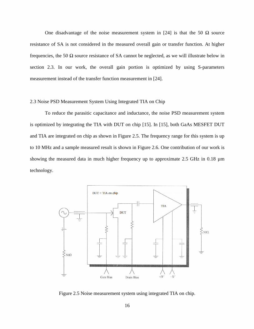
To reduce the parasitic capacitance and inductance, the noise PSD measurement system
is optimized by integrating the TIA with DUT on chip [15]. In [15], both GaAs MESFET DUT
and TIA are integrated on chip as shown in Figure 2.5. The frequency range for this system is up
to 10 MHz and a sample measured result is shown in Figure 2.6. One contribution of our work is
showing the measured data in much higher frequency up to approximate 2.5 GHz in 0.18 µm
technology.
Figure 2.5 Noise measurement system using integrated TIA on chip.

17
Figure 2.6 A sample noise power measured result [5].
2.3.1 Noise Measurement System in the Thesis
SiGe HBTs are widely used to design low noise amplifier [26]. In our project, we use a
new TIA which has a bandwidth up to 2.5 GHz to allow us to detect the white noise component
beyond the 1/f noise corner frequency. As shown in Figure 2.7, DUT and TIA are AC coupled
and the output impedance of the DUT plus resistor on drain node is much larger than the
equivalent input impedance of Cc plus TIA part, so that the drain current noise current id can
flow into the TIA and be amplified there. A voltage buffer with an output impedance of 50 Ω is
used to drive a 50 Ω spectrum analyzer.
The size of DUT is: W/L= 100 3.2 / 0.18 µm, where 100 is the number of gate figures,
3.2 µm is the gate finger width. As discussed in section 1.2, the chosen size of DUT affects noise
measurement. With increasing the channel width, the thermal noise increases while 1/f noise

18
decreases. Hence the corner frequency decreases, making the thermal noise easier to measure.
However, the channel width cannot go to infinity. One important reason is that the output
impedance of DUT decreases with increasing the channel width.
Figure 2.7 Noise measurement system using SiGe TIA on chip.
Figure 2.8 Die photo with DUT and TIA on chip.

19
Figure 2.8 shows one test die under microscope. The big circle on the right contains the
DUT and TIA in circuit. The circle on the left contains the standalone NMOS which is designed
to be the same structure as the NMOS in the circuit, and the size of the NMOS is the same as
DUT in circuit. The standalone NMOS is used for DC and RF characteristics.
In Figure 2.7, DC pad VCC is used to connect DC power supply for TIA. DC pad VDD is
used to connect DC power for drain terminal of the DUT. There is a resistor RDD between VDD
and drain terminal to avoid drain current noise flow out from VDD pad. Because that RDD
produces noise in, RDD = DDRKT /4 , to ignore in, RDD when measuring drain current noise
id= 04 dsgKT , in, RDD should much less than id, which means 0
1ds
DD
gR
is around 1, so ץ .
0
1
ds
DDg
R . In our work, 0dsg is in the range of 30 mS to 80 mS, so 0
1
dsg is approximately
from 10Ω to 30 Ω. Hence, 2 KΩ is a big enough value for DDR . Since there is a resistor RDD
between VDD and drain terminal, the value of VDD is much higher than the voltage applied to
drain terminal. If DDR is too large, VDD need to be very high to achieve a certain VDS, which may
exceed the range of DC power supply. A tiny current source iDS, such as10 nA, is applied to DC
pad VDS to monitor the voltage actually applied to drain terminal VDS. DC pad VGS or AC pad IN
is used to connect power supply for the gate. There is a 20 KΩ resistor Rg,bias between VGS pad
and the gate terminal.

20
Figure 2.9 Simplified equivalent circuit for noise from Rg,bias.
Consider the noise from Rg,bias as an equivalent voltage noise source VRg,bias in Figure 2.9,
the PSD of drain current noise from Rg,bias Rgbiasid,S can be calculated as
2
,
22
2
,
22
Rgbiasid,,Rm,Rm
S
biasg
in
biasgin
in
R
ZVg
RZ
ZVg
biasgbiasg
(2.3)
where Zin is equivalent input impedance approximately 100 Ω, gm is the transconductance of the
DUT, and the square of equivalent input voltage for Rgid ,S , 2
,RgbiasinV , is given by
noisegnoiseg
in
R
ZKT
R
ZKTRV in
biasgRgbiasin
,
22
,
2 44 ,,
(2.4)
To ignore Rgbiasid,S , 2
,RgbiasinV in equation (2.4) should be much smaller than
2
04
mg
gKT ds .
2
0
mg
g ds and
inZ can be acquired by DC measurement and S-parameters measurement which are discussed in
detail in Appendix A and B, respectively. So we can choose a large enough value for Rg,bias.
21
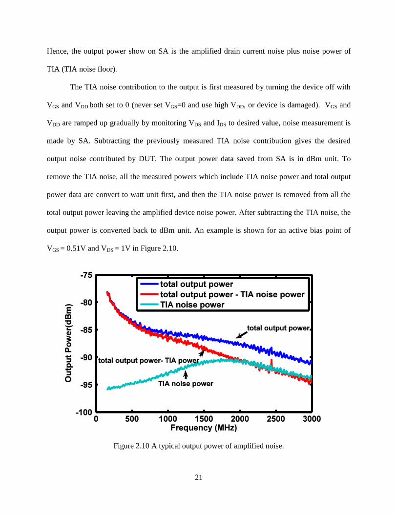
Hence, the output power show on SA is the amplified drain current noise plus noise power of
TIA (TIA noise floor).
The TIA noise contribution to the output is first measured by turning the device off with
VGS and VDD both set to 0 (never set VGS=0 and use high VDD, or device is damaged). VGS and
VDD are ramped up gradually by monitoring VDS and IDS to desired value, noise measurement is
made by SA. Subtracting the previously measured TIA noise contribution gives the desired
output noise contributed by DUT. The output power data saved from SA is in dBm unit. To
remove the TIA noise, all the measured powers which include TIA noise power and total output
power data are convert to watt unit first, and then the TIA noise power is removed from all the
total output power leaving the amplified device noise power. After subtracting the TIA noise, the
output power is converted back to dBm unit. An example is shown for an active bias point of
VGS = 0.51V and VDS = 1V in Figure 2.10.
Figure 2.10 A typical output power of amplified noise.

22
The output power decreases from -78 dBm at 100 MHz to -92 dBm at 3 GHz. noiseoN , ,
PSD of the output power, is then calculated and expressed in unit of dBm/Hz as follows [27, 28]:
BWP dBmout 1010noiseo, log10|BWmW1
Plog10N
(2.5)
where BW is measurement bandwidth, and is determined by resolution bandwidth RBW in SA
settings [29]. The voltage spectral density VSD of amplified drain current noise noiseoV , (V/ Hz )
by converting power to voltage which is given by
o
noiseNo
noiseo Z3
10
,
, 10V (2.6)
where Zo = 50 Ω is the SA input impedance. Figure 2.11 and 2.12 are noiseoN , and noiseoV , for the
same bias set VGS = 0.51V and VDS = 1V as Figure 2.10.
Figure 2.11 A typical output power spectral density of output power.

23
Figure 2.12 A typical output VSD.
Consider the noise measurement system in Figure 2.7 as an equivalent input referred
noise voltage source noiseinV , added to a noiseless circuit as shown in Figure 2.13. noiseoV , has been
acquired above. The drain current noise id related to noiseoV , by
totalnoiseo ZidV , (2.7)
where bufferTIAtotal AZZ , TIAZ is TIA gain, bufferA is buffer voltage gain. To get totalZ , an input
voltage signal Vin which is large enough to ignore id is added to input port of the network shown
in Figure 2.13. The output voltage of the test signal Vout is given by
totalminout ZgVV . (2.8)
Using equivalent (2.7) and (2.8), an input referred noise voltage noiseinV , can be defined as
in
out
noiseo
noisein
V
V
VV
,
, . (2.9)

24
Such that noiseinmVg ,id . So the next question is to find in
out
V
V. In [24], a spectrum analyzer is
used. This however cannot account for the 50 Ω source resistance, which is not negligible for
high frequency, where Zin is only 100 Ω in Figure B.17. We solve this problem using S-
parameters measurement. The S-parameters can be converted to Y-parameters which we can use
to find in
out
V
V as below.
Figure 2.13 Noise measurement system equivalent circuit.
Figure 2.14 Equivalent two ports network.

25
Consider a two port network as shown in Figure 2.14, and apply an input test voltage Vin
with a Zo load, the current at port 2 I2 is given by [30]
1212222 YY VVI (2.10)
where V1 and V2 are the voltages at port 1 and 2, respectively. Y-parameters Y21 and Y22 can be
calculated from S-parameters by [27]
21122211
21
o
12SSS1S1
2S-
Z
1Y
—))(( (2.11a)
21122211
21122211
o
22SSS1S1
SSS1S1
Z
1Y
—))((
))((
(2.11b)
Substituting oZ
VI 2
2 - , outV = 2V and inV = 1V into equation (2.10), in
out
V
V is obtained as
o
o
in
out
Z
Z
V
V
V
V
22
21
1
2
Y1
Y
. (2.12)
Using equation (2.9) to (2.12), we can calculate noiseinV , from noiseoV , and S-parameters. noiseoV , has
been acquired from noise spectrum measurement discussed above and standard on-wafer S-
parameters measurement is discussed in Appendix B. noiseinV , (V/ Hz ) at bias VGS = 0.51V and
VDS = 1V is plotted in Figure 2.15, noiseinV , decreases from 100 MHz to 2 GHz, and then it
becomes independent of frequency from 2 GHz to 3 GHz.

26
Figure 2.15 A typical noiseinV , ( V/ Hz ) vs frequency.
The drain current noise PSD Sid can now be calculated from gate-referred noise voltage
noiseinV , by
2
,inid )(S noisemVg . (2.13)
Sid at VGS = 0.51V and VDS = 1V is shown in Figure 2.16.

27
Figure 2.16 A typical Sid (A2/Hz) vs freqency .
From Figure 2.16, we can see the corner frequency for our DUT is around 2 GHz. Sid at
lower frequencies is nearly proportional to 1/f. Sid of the thermal noise component beyond 1/f
corner frequency is 1.8×10⁻²²
A2/Hz. When frequency is higher than 2.5 GHz, Sid increases a
little near 3 GHz. The possible reason is the poor performance of TIA in that frequency range
which is discussed in section 3.2.2.
Since noise factor ץ is widely used in literatures to demonstrate the enhanced channel
thermal noise in short channel transistors. After extracting Sid, the noise factor ץ is derived using
equation (1.3). For bias set VGS = 0.51V and VDS = 1V, ץ is shown in Figure 2.17.

28
Figure 2.17 Noise factor ץ versus frequency.
2.3.2 SiGe HBT TIA
To use TIA as the low noise amplifier, the system must satisfy two requirements to make
sure the device noise can be resolved from other noise [8] because that the device noise is not the
only noise source in the measurement system. The first requirement is that the amplified noise of
the device must be greater than the input noise of the spectrum analyzer which is the SA noise
floor. The second requirement is that the equivalent input noise of the amplifier which is the TIA
noise floor must be less than the device noise.
In both triode and saturation regions of the MOSFET, the noise amplifier should be
driven in a large resistances region presented by the DUT. In the saturation region of MOSFET,
MOSFET works like a high resistance current source at output terminal. This phenomenon
requires that the amplifier following the MOSFET has a low equivalent input current noise.
In our work, SA noise floor is the noise measurement result for only SA and the cable
between output probe and SA. TIA noise floor is the noise measurement result when DUT turned
off. NMOS device (DUT) amplified noise is measured when both DUT and TIA are biased.

29
Figure 2.18 A typical output PSD of NMOS + TIA system, TIA noise floor and SA noise floor
versus frequency
As shown in Figure 2.18, the TIA satisfies all the design requirements described above.
Comparing the NMOS biased and SA noise floor curves, we see the amplified noise of the
device is greater than SA noise floor. Comparing the NMOS biased and TIA noise floor curves,
we know that the TIA noise floor is less than the amplified device noise.
30
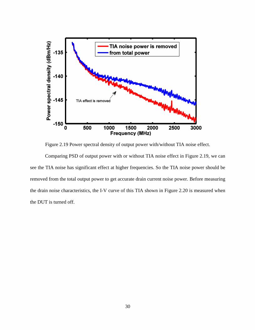
Figure 2.19 Power spectral density of output power with/without TIA noise effect.
Comparing PSD of output power with or without TIA noise effect in Figure 2.19, we can
see the TIA noise has significant effect at higher frequencies. So the TIA noise power should be
removed from the total output power to get accurate drain current noise power. Before measuring
the drain noise characteristics, the I-V curve of this TIA shown in Figure 2.20 is measured when
the DUT is turned off.

31
Figure 2.20 Measured I-V curve of TIA with DUT biased off
Figure 2.20 shows this TIA turns on at VCC = 1.5V and the Icc-Vcc behaves like a resistor
at VCC > 2.5V. A Vcc = 4.25 V is used in this work.
From equation (2.8) totalZ can be calculated by
min
totalgV
V 1Z out . (2.14)
Figure 2.21 A typical totalZ vs frequency.

32
Figure 2.21 shows the total gain versus frequency at VGS = 0.51V and VDS = 1V. Gain is
constant below 2 GHz, drops to half values at 3 GHz, indicating a 3 dB bandwidth of 2.6 GHz.
The noiseness in the lower frequency range normally comes from S-parameters. From total gain
and measured TIA and buffer noise voltage tiaoV , , PSD of the TIA and buffer current noise BTIA,i ,
tiaS , is obtained as
2
2
,2
,iStotal
tiao
BTIAtiaZ
V (2.15)
For VGS=0.55V, VDS=1V, tiaS is shown in Figure 2.22. tiaS is 610-23
A2/Hz for frequency
lower than 1 GHz, and it increases to 2.510-22
A2/Hz from 1 GHz to 3 GHz. Comparing Figure
2.22 and Figure 2.16, we can see that Sid is smaller than tiaS when frequency is higher than 2
GHz, which indicates the noise from TIA is not negligible at high frequencies in drain current
noise measurement.
Figure 2.22 A typical tiaS and Sid vs frequency.
33
Chapter 3
Noise Measurement and Data Analysis
After boosting the noise though TIA, the output power of the noise can be measured by
spectrum analyzer (SA). Drain current noise is extracted from the measured and calculated
NMOS + TIA system parameters data. Noise factor ץ is calculated from measured Sid in the
white noise range of the measured drain current noise spectrum.
3.1 Noise Measurement
Figure 3.1a and Figure 3.1b show the noise measurement equipment setup used in our lab.
On the left is a HP 4155 semiconductor analyzer, which we use to characterize DC I-V,
transconductance gm, output resistance Rout, as well as to supply power to both DUT terminals
and VCC of TIA. The metal box in front of the probe station adapts BNC connectors of the cables
from the DC biasing probes to the special SMU cable connectors. The output power of amplified
drain current noise is measured using a PSA series spectral analyzer, shown on the right. At the
TIA output, a bias tee is used between the TIA output and SA to block DC and pass AC. As
described in Appendix A and Appendix B, the measurement system needs to change during DC
measurement and S-parameters measurement.

34
Figure 3.1a Drain current noise measurement system setup.
Figure 3.1b Drain current noise measurement system diagram.

35
Figure 3.2 Block diagram of operation theory for spectrum analyzer [29].
Figure 3.2 shows block diagram of a spectrum analyzer. The input signal to be analyzed
and the synchronous local oscillator signal which is generated by gate controlled scan generator
are combined at the mixer. After passing the IF resolution bandwidth (RBW) filter, the filtered
IF output goes through a log amplifier and is detected by an envelop detector. Then the signal
passes through a video bandwidth filter which is used to decrease peal-to-peak variations of
noise to a peak/sample detector. Then the signal passes through a video bandwidth filter which is
used to decreasing the peal-to-peak variations of noise to a peak/sample detector. The display
logic modify the horizontal (frequency) axes. The peak/sample detector detects and passes the
signal to analog-digital converter to transfer the analog signal into digital signal to allow the
spectrum analyzer to display the signal.
Considering the operation theory of SA [27-30], the following SA setting are used:
Frequency range: 100 MHz ~ 3 GHz, Resolution Bandwidth (RBW on instrument panel) = 300
KHz, Video Bandwidth (VBW on instrument panel) = 3 KHz, Video Bandwidth/Resolution

36
Bandwidth = 0.01, Reference level = -60 dBm and Attenuation = 0dB. The default value of
RBW is 3 MHz on SA we used. After changing it to 300 KHz, we compare these two measured
results by overlay them in one figure and the figure shows taht these two curve are totally
coincident. It demonstrates that both 3 MHz and 300 KHz work well for RBW setting in our
work. The ratio of VBW/RBW is usually set to 0.1 or 0.01, which is small enough for accurate
measurement result as described in [28].
Figure 3.3 Die photo with right AC probe and DC probes on pads.
Figure 3.3 shows a photo of the die and probe configuration during noise power
measurement. A Cascade Infinity GSG probe contacts the GSG pads at the TIA output, and
connects the output to SA input. The Eye-Pass DC probe, shown in Figure 3.4, is used to contact
all the DC pads and supply power to TIA through the VCC pad, to DUT gate through the VGS pad,
and to DUT drain through the VDD pad. The capacitance Cp in Figure 3.1b is 10 nF as shown in
Figure 3.4 to keep AC ground from these pads. The ground tip showed in Figure 3.4 is contacted
to our designed ground pad one to one.

37
Figure 3.4 Configuration of Eye-Pass DC probes (Cascade Microtech Company).
3.2 Experimental Results Analysis
The drain current spectral density and noise factor from all the bias set we chose are
shown in Figure 3.5. Figure 3.6 and Figure 3.8 demonstrate the voltage dependence of ץ and Sid
respectively.
38
Figure 3.5 Drain current noise spectral density Sid and noise factor ץ versus VDS.
Figure 3.6 Noise factor ץ with different biases.

39
Figure 3.7 Extracted noise factor ץ vs VGS in 0.18 µm technology [14].
Same as plots in Figure 3.7, we can see that ץ in Figure 3.6 decreases with increasing VGS
at fixed VDS, and it increases with increasing VDS at fixed VGS.

40
Figure 3.8 Drain current noise PSD Sid vs Vgs.
Figure 3.9 Drain current noise PSD Sid vs Vgs in 0.18 µm technology [6].

41
Same as plots in Figure 3.9, Sid in Figure 3.8 increases with raising VGS at fixed VDS and
it also increases with increasing VDS at fixed VGS. Figure 3.10 shows that Sid increases with IDS at
fixed VDS. This phenomenon is also shown in Figure 3.11 [31].
Figure 3.10 Drain current noise PSD Sid vs drain current IDS.
Figure 3.11 Drain current noise PSD Sid vs drain current IDS in 90 nm technology [31].

42
As mentioned in Chapter 2, TIA is not noiseless and its noise power should be removed
from the total measured noise power. Figure 2.15 shows us the noise floor of this SiGe TIA in
green curve is only 3 or 4 dBm/Hz lower than the amplified noise power density in red curve
when frequency is higher than 1.5 GHz. In other words, the noise of TIA is not negligible at
higher frequency. To remove the TIA noise effect from measured drain current noise, we
subtract TIA noise power from the total measured output power. And the result is shown in
Figure 3.12.
Figure 3.12 Comparison of output noise power
From Figure 3.12 we can see the measured output power without the effect of TIA which
shown in red curve is lower than the total output power which contains the power of TIA noise.
This phenomenon is obvious when frequency is higher than 1.5 GHz.

43
After subtracting the TIA noise power from the total measured power, the derived drain
current noise PSD and noise factor are shown in Figure 3.13 and Figure 3.14.
Figure 3.13 Comparison of Sid
Figure 3.14 Comparing of ץ

44
Actually, the TIA noise floor which shown in Figure 2.15 is not exactly the same as
equivalent TIA noise when DUT is biased. Therefore, there is an approximation. A better way to
remove the TIA noise effect from measured drain current noise is need to do as the future work.
Moreover, the error bar of noise measurement on SA is approximately 1 dBm, which also affects
the final experimental result.
Figure 3.15 Sid vs frequency at fixed VGS.

45
Figure 3.16 Sid vs frequency at fixed VDS.
Figure 3.15 and Figure 3.16 show Sid versus frequency at fixed VGS or fixed VDS. For
both 1/f noise component and thermal noise component, Sid increases with VDS at fixed VGS and
Sid increases with VGS at fixed VDS. The corner frequencies only change a little at these bias.

46
Appendix A
On-Wafer DC Measurements
A.1 Introduction
As mentioned in Chapter 1, to derive the drain current noise spectral density and noise
factor, we need to measure transconductance (gm) and drain-source conductance (gds). Hence,
DC I-V measurements need to be done to acquire these parameters. Besides, we can see the
mathematical relationship between the voltages and current at each terminal and know the
operating limits of the transistor.
Figure A.1 DC measurement system setup

47
This measurement system was controlled by ICCAP software through GPIB-USB
connected to probe station and HP4155 semiconductor parameter analyzer which was used to
supply DC power through bias box.
Figure A.2 Die photo with DUT and TIA on chip
One test die under microscope is shown in Figure A.2. The red circle contains the DUT
and TIA in circuit. The blank circle contains the standalone NMOS which is designed to be the
same structure as the NMOS in the circuit, and the size of the NMOS is the same as DUT in
circuit. The reasons putting a standalone NMOS here are using the space on wafer efficiently and
see some basic DC and RF characteristics.

48
A.2 DC Measurements for Standalone MOSFET
To know to basic characteristics of the transistor, DC measurements for standalone
MOSFET was carried out at first. As shown in Figure A.3, two Ground-Signal-Ground AC
probes was used to test the standalone NMOS.
Figure A.3 Die photo with AC (G-S-G) probes on standalone NMOS pads
A.2.1 IDS-VDS and IDS-VGS Measurements
Figure A.4 Measured IDS-VDS for standalone NMOS

49
Considering the output characteristic of the transistor shown in Figure A.4, most of the
drain biases we chosen, such as 0.46V, 0.73V and1V, are in the saturation regions. To compare
the noise characteristics in saturation region which are interested in most cases, we also chose
0.18V in triode region as the drain bias.
Figure A.5 Measured IDS-VGS for standalone NMOS
Considering the transfer characteristic of the transistor shown in Figure A.5, most of the
gate biases we chosen, such as 0.55V, 0.58V, 0.61V and 0.64V, are in the moderate and strong
inversion regions.
A.2.2 gds and gm
In A.2.1, we got the measurement result for IDS-VDS and IDS-VGS. To acquire gds and gm
which are used for noise spectral density and noise factor extraction, equation (1.2) and (1.6) are
used and the calculation results are shown in Figure A.6 and Figure A.7 separately.

50
Figure A.6 Gate-source conductance gds vs VDS
Figure A.7 Transconductance gm vs VGS

51
Also, we can check the output resistance of the transistor Ro from gds, which is shown in
Figure A.8. The resistances are several hundreds of Ohms for these bias sets, which require the
equivalent of input impedance of TIA part be less to allow drain current noise current flow into
TIA.
Figure A.8 Output resistance of the NMOS vs VDS
A.3 DC measurements for Integrated DUT in Circuit
A.3.1 Measurement Equivalent Circuit
DC measurements for integrated MOSFET with TIA in circuit are more complex than
DC measurements for standalone MOSFET since IDS-VDS and IDS-VGS measurements cannot be
measured directly.
52
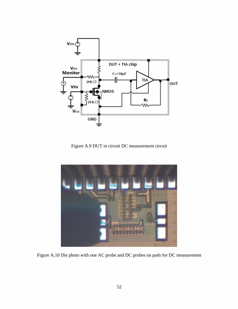
Figure A.9 DUT in circuit DC measurement circuit
Figure A.10 Die photo with one AC probe and DC probes on pads for DC measurement

53
Figure A.9 shows the equivalent circuit for DUT DC measurement. VDD and IN provide
DC voltage for drain and gate separately. VDS probe is used to monitor drain voltage by adding a
tiny current source iDS at VDS pad, such as 10 nA. With this small current, the voltage drop can be
ignored so that the tested voltage shown on VDS is very close to drain voltage. Also, because
there is a 2 KΩ resistor between VDD pad and drain terminal, VDD is not the voltage value we add
to drain. In case of damaging the DUT, we have to estimate the VDD using
DDDSGS RIV DDV (A.1)
where VGS is the operating voltage added to drain terminal, RDD = 2 KΩ, measured current IDD
from VDD pad is the drain current IDS which should be similar value in standalone NMOS DC
measurement result.
Compared with Figure A.9, Figure A.10 tells how the real probe pads matched the pins in
the electrical circuit.
A.3.2 IDS-VDS measurement and gm Extraction
Because IDS-VDS for the DUT cannot be measured directly, we need to do IDD-VDD and
VDS-VDD measurement first, and then show the data using IDD-VDS axes. Attention is IDD = IDS as
we talked before.

54
Figure A.11 Measured IDS-VDS for integrated DUT in circuit
Figure A.11 shows the output characteristic of the integrated DUT in circuit. To compare
with the DC measurement result for standalone NMOS and integrated DUT in circuit, the IDS-
VDS plots from Figure A.4 and Figure A.11 are overlay by Figure A.12.
Figure A.12 Comparing IDS-VDS for both integrated DUT in circuit and standalone NMOS

55
For the manufacture reason, there are slight differences between the DC characteristics of
standalone NMOS transistor and the integrated DUT in circuit. The drain current difference
increases with raising gate voltage or drain voltage.
Similar to standalone NMOS DC measurement, using equation (1.2), gds could be derived
from IDS-VDS. And gds of this DUT in circuit is shown in Figure A.13
Figure A.13 gds of integrated DUT in circuit
To acquire gm of integrated DUT, there are two methods. The first one is get gm from gm
–VGS measurement data for standalone NMOS. The second method shown in Figure A.14 is
chosen very close to values of VGS, using the difference of the nearby IDS values as SDI and
using the difference of the nearby VGS as SGV . In this method, gm is given by
13
13
mgGSGS
DSDS
VV
II
(A.2)

56
Figure A.14 IDS-VDS for nearby VGS
Keep the Figure A.12 in mind; it is more appropriate to use the second method to derive
gm for higher biases set.

57
Appendix B
On-Wafer S-Parameters Measurement
B.1 Introduction
Scattering parameters (S-parameters) are power wave descriptors that used to define the
input-output relations of a network, which is a two port network in our work, in terms of incident
and reflected power waves.
Figure B.1 Convention for defining S-parameters for two-port networks
Normalized incident power wave an and reflected power wave bn are given by
)(2
1non
o
n IZVZ
a (B.1a)
)(2
1non
o
n IZVZ
b (B.1b)
where n is port number 1or 2, Zo = 50 Ω is the characteristic impedance of the connecting lines
on the input or output side of the network. Vn and In are input or output voltage and current. And
based on Figure B.1, S-parameters are defined by
]][[][ nn aSb (B.2)

58
where S11 is the ratio of reflected to incident power wave at port 1; S22 is the ratio of reflected to
incident power wave at port 2; S12 is the ratio of transmitted power wave at port 1 to incident
power wave at power 2; S21 is the ratio of transmitted power wave at port 2 to incident power
wave at power 1.
By matching on the input or output side, S-parameters can be determined. Figure B.2
shows the simple equivalent circuit of S11 and S21 measurement, where the line impedance Zo is
matched through a corresponding load impedance ZL = Zo for a2 = 0 at the output side.
Figure B.2 Measurement of S11 and S21 by matching the line impedance Zo at port 2 through a
corresponding load impedance ZL = Zo
From Figure B.2, we can calculate S11 by the input reflection coefficient in :
oin
oin
inZZ
ZZS
11 (B.3)
On other hand, we can acquire Zin from S11 by changing the form of equation B.3 to
11
11
1
1
S
SZZ oin
(B.4)
Besides, from equations B.1a, equation B.1b and Figure B.2, we can calculate S21 by
11
20
1
221
2|S
2 IZV
V
a
b
o
a
(B.5)

59
where V1 = VS1 - ZoI1 and V2 is the output voltage Vout. Hence, we can reform equation to
1
out
21
2S
sV
V (B.6)
Since the voltage at port 2 is directly related the source voltage, available forward voltage
gain can be get from S21 in dB unit by
||log20 21, SG avv (B.7)
Figure B.2 also represent that input voltage can be acquired by
ino
in
sinZZ
ZVV
(B.8)
Similar to measurement of S11 and S21 the measurement circuit (Figure B.3) of S22 and
S12 can be considered as a reflection of Figure B.2 by matching the line impedance Zo through a
corresponding input impedance ZG = Zo
Figure B.3 Measurement of S22 and S12 by matching the line impedance Zo at port 1 through a
corresponding input impedance ZG = Zo

60
B.2 S-Parameters Measurement System
For S-parameters measurement system setup shown in Figure B.4, GPIB-USB was used
to connect Agilent PNA E8464B network analyzer, HP4155 and a computer which offered
ICCAP software. After setting up the measure/simulation and instrument option sections in
ICCAP, HP4155 and PNA can be controlled automatically. HP4155 which works as DC power
supply and PNA which works as AC power supply are connected to Probes through bias T.
Power meter is connected to PNA by GPIB-USB to help with the power calibration portion
during S-parameters measurement.
Figure B.4 S-parameters measurement system

61
Figure B.5 Simplified block diagram of the PNA network analyzer system
As shown in Figure B.5, a phase-locked incident signal which includes both reference
signal and test signal is generated from the synthesized source. Through the signal separation
portion of the PNA, the reference signal was received by the receiver portion and the test signal
is applied to the device under test (DUT) through port 1 and port 2. In this work, port 1 is
selected as the source port as shown in Figure B.6.
In the test system, random and systematic measurement errors are involved in the S-
parameters measurement. Although some random errors, such as thermal drift, cannot be
removed systematically, the systematic error of the PNA network analyzer and the power loss of
the cables can. In our work, the calibration standard technique short-open-load-through (SOLT)
which uses testing and calculating short, load and through standard parameters to remove errors
is used with Cascade impedance standard substrate ISS 101-190B which fit our AC probes and
shown in Figure B.6.

62
Figure B.6 Layout of Cascade impedance standard substrate 101-190B (Cascade Microtech Inc.)
B.3 S-Parameters Measurement for Standalone MOSFET
Similar to DC measurement, S-parameters measurement for standalone MOSFET was
carried out first to check the setup of measurement system, the measurement method and RF
performance of the transistor. The S-parameters measurement circuit is shown in Figure B.7. The
DC power from HP4155 and AC power from PNA are combined in bias Ts and the output
signals go into the NMOS through AC pads IN and OUT.

63
Figure B.7 Circuit of the S-parameter measurement system for standalone NMOS
Take biases set VGS = 0.55V and VDS = 1V (IDS = 4.5 mA) for example, the measurement
results is shown in Figure B.8:
Figure B.8 Real and image parts of S-parameters versus frequency for standalone NMOS
Changing these data into dB unit by SdB = 20 log |S|, we can see Figure B.9
64
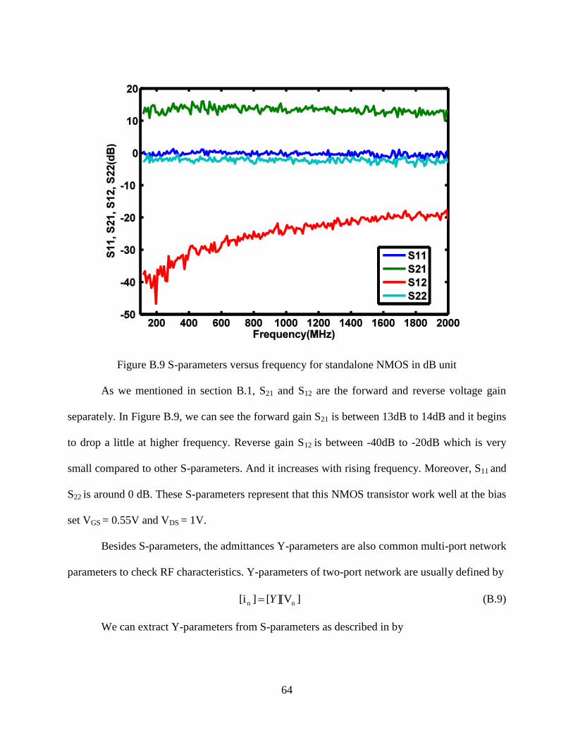
Figure B.9 S-parameters versus frequency for standalone NMOS in dB unit
As we mentioned in section B.1, S21 and S12 are the forward and reverse voltage gain
separately. In Figure B.9, we can see the forward gain S21 is between 13dB to 14dB and it begins
to drop a little at higher frequency. Reverse gain S12 is between -40dB to -20dB which is very
small compared to other S-parameters. And it increases with rising frequency. Moreover, S11 and
S22 is around 0 dB. These S-parameters represent that this NMOS transistor work well at the bias
set VGS = 0.55V and VDS = 1V.
Besides S-parameters, the admittances Y-parameters are also common multi-port network
parameters to check RF characteristics. Y-parameters of two-port network are usually defined by
][V][]i[ nn Y (B.9)
We can extract Y-parameters from S-parameters as described in by

65
21122211
21122211
o
11SSS1S1
SSS1S-1
Z
1Y
—))((
))((
(B.10a)
21122211
12
o
21SSS1S1
2S-
Z
1Y
—))(( (B.10b)
21122211
21
o
12SSS1S1
2S-
Z
1Y
—))(( (B.10c)
21122211
21122211
o
22SSS1S1
SSS1S1
Z
1Y
—))((
))((
(B.10d)
And the calculation results is shown in Figure B.10
Figure B.10 Y-parameters versus frequency for standalone NMOS

66
B.4 S-Parameters Measurement for integrated DUT and TIA System
The electrical circuit for S-parameters measurement for DUT and TIA is shown in Figure
B.11.
Figure B.11 S-parameters measurement system circuit
In this measurement system, the DUT and TIA are considered as a whole system.
HP4155 is used to provide DC power for NMOS and TIA through RF pad IN, DC pads VDD and
VCC. In this measurement, DC pads, RF pads IN and OUT all are connected to the probes like
shown in Figure B.12.

67
Figure B.12 Die photo with two AC probe and DC probes on pads for S-parameters
measurement
One attention for S-parameters measurement is choosing the power value on PNA. When
frequency = 1GHz, Vds = 1 V and Vgs = 0.51 V, as shown in Figure B.13, the source power
chosen for our work is -60 dBm which is small enough to neglect its effect on DC characteristics
and also not too small to cause the RF characteristic distortion for our project.
Figure B.13 Power sweep for S-parameters measurement

68
For an instance, the tested S-parameters for the DUT and TIA system at bias set VGS =
0.51V, VDS = 0.18V is shown in Figure B.13
Figure B.14 S-parameters versus frequency for NMOS + TIA
In Figure B.14, S21 of the NMOS + TIA system keeps staying at 42 dB from 100 MHz to
1.50 GHz at 42 dB, and after 1.50 GHz, it drops from 28 dB to 23 dB. The reverse voltage gain
S12 is between -60 dB to -40 dB. S11 keeps staying at 0 dB at lower frequency and it begins to
drops approximately after 1.50 GHz. At 3 GHz, it drops to -3 dB. S22 decreases from -1 dB to -4
dB from 400 MHz to 3 GHz.
Besides, we can get equivalent input impedance of this NMOS + TIA system Zin from S-
parameters.

69
Figure B.15 Equivalent input impedance versus frequency for NMOS + TIA
Figure B.15 shows us that the real part of the equivalent of the input impedance seems
like a resistor which values R = 36 Ω and is almost not changed with frequency after 500 MHz.
Neglecting the effect of inductance, the image part of the input impedance )( inZ is given by
Ci
1Z in )( (B.111)
From equation B.13, we can derive equivalent input capacitance C to be
)( inZ
1-C
(B.12)

70
Figure B.16 Equivalent input capacitance versus frequency for NMOS + TIA
Equivalent input capacitance shown in Figure B.16 is around 0.8 pF. The equivalent input
impedance can be considered as the resistor and capacitor in series. From Figure B.15 and Figure
B.16, the magnitude of the equivalent input impedance can be calculated by
Ci
1RZ in . (B.13)
The magnitude of equivalent input impedance is shown in figure B.17.
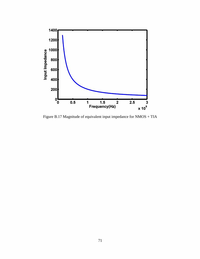
71
Figure B.17 Magnitude of equivalent input impedance for NMOS + TIA

72
Bibliography
[1] A. van der Ziel, "Noise in Solid-state Devices and Lasers," proceeding of the IEEE, vol. 58,
No. 8, August 1970.
[2] Y. Nemirovsky, I. Brouk and C. G. Jakobson, "1/f Noise in CMOS Transistors for Analog
Applications," IEEE transactions on electron devices, vol. 48, No. 5, May 2001.
[3] A. Hati, D. A. Howe, F. L. Walls and D. Walker, "Noise Figure vs. PM Noise Measurements:
A Study at Microwave Frequencies," IEEE International Frequency Control Symposium and
PDA Exhibition, 2003.
[4] Y. Tsividis, Operation and Modeling of The MOS transistor, McGraw-Hill Inc., 1999.
[5] J. B. Johnson,"Thermal Agitation of Electricity in Conductors," Phys. Rev. 32, 97–109, 1928.
[6] A. Van der Ziel, "Thermal Noise in Field-Effect Transistors", Proc. of the IRE, vol. 56, pp.
1808-1812, August 1962.
[7] C. Chen and M. J. Deen,"Channel Noise Modeling of Deep Submicron MOSFETs, "IEEE
IEEE transactions on electron devices, vol. 49, No. 8, August 2002.
[8] J. C. J. Paasschens, A. J. Scholten, and R. van Langevelde, "Generalizations of the Klaassen-
Prins equation for calculating the noise of semiconductor devices", IEEE transactions on
electron devices, vol. 52, No. 11, November 2005.
[9] A. A. Abidi, "High-Frequency Noise Measurements on FET’s with Small Dimensions," IEEE
transactions on electron devices, vol. ED-33, No. 11, November 1986.
[10] S. Dronavalli and R. P. Jindal, "CMOS Device Noise Considerations for Terabit Lightwave
Systems,” IEEE transactions on electron devices, vol. 53, No. 4, April 2006.
[11] C. Chen, "Thermal Noise in Modern CMOS Technology," Solid State Circuits Technologies,
InTech, 2010.
[12] C.Chen, M.J.Deen, M. Matloubian and Y. Cheng, "Extraction of the induced gate noise,
channel thermal noise and their correlation in sub-micron MOSFETs from RF noise
measurements," Microelectronic Test Structures, 2001. ICMTS 2001.
[13] B. M. Wilamoski and D. Irvin, Fundamentals of Industrial Electronics, Taylor & Francis
Group, 2011

73
[14] K. Han, K. Lee and H. Shin, "Thermal Noise Modeling for Short-Channel MOSFET’s,"
Simulation of Semiconductor Processes and Devices, SISPAD 2003.
[15] K. Yan, Noise Measurements, Models and Analysis in GaAs MESFETs Circuit Design,
PHD dissertation, Oregon State University, 1996.
[16] H. A. Haus et al., "Representation of Noise in Linear Twoports", Proc. IRE, vol. 48, no. 1,
pp. 69–74, Jan. 1960.
[17] H. Rothe and W. Dahlke, “Theory of noisy fourpoles,” Proceedings of the IRE, Vol. 44, , pp.
811–818, June 1956.
[18] L., R. Q., "The determination of device noise parameters". Proc. of the IEEE, Vol. 57, No. 8,
pp. 1461-1462, Aug. 1969,
[19] M. Mitama, and H. Katoh, "An improved computational method for noise parameter
measurement," IEEE Trans. Microwave Theory Tech., Vol. MTT-27, No. 6, pp. 612-615, June
1979.
[20] G. I. Vasilescu, G. Alquie, and M. Krim, "Exact computation of two-port noise parameters,"
Electron. Lett. , pp. 292-293, Vol. 25, No. 4, Feb. 1988.
[21] O'Callaghan, J.M. and Mondal, J.P,"A vector approach for noise parameter fitting and
selection of source admittances",IEEE Trans. Microwave Theory Tech., Vol. 28, No. 8, pp.
1376-1382. Aug.1991.
[22] C. H. Chen, et al., "Novel noise parameter determination for on-wafer microwave noise
measurements". IEEE Trans. Instrum. Meas., Vol. 57, Issue 11, pp. 2462-2471, May 2007.
[23] L. F. Tiemeijer, R. Havens, R. Kort, and A. J. Scholten, "Improved Y-factor method for
wide-band on-wafer noise parameter measurements," IEEE Trans. Microw. Theory Tech., vol. 53,
no. 9, pp. 2917–2925, Sep. 2005.
[24] S. Tedja, H.H. Wiliams, J. van der Spiegel, F.M. Newcomer and R. Van Berg. "Noise
Spectral Density Measurements of a Radiation Hardened CMOS Process in the Weak and
Moderate Inversion," IEEE Transactions on Nuclear Science. Vol. 39(4). pp. 804-808, 1992.
[25] S. Tedja, "Analytical and Experimental Studies of Thermal Noise in MOSFET's", IEEE
transactions on electron devices, vol. 41, No. I I , Novenber 1994.
[26] J. Cressler and G. Niu, Silicon-Germanium Heterojunction Bipolar Transistors. Boston,
MA/USA: Artech House, INC., 2002.
[27] Making RF Power and Frequency Measurements with Spectrum and Signal Analyzers,
Agilent Technologies, Inc. 2012

74
[28] Agilent Technologies E8362B, E8363B and E8364B Option H85 User’s and Service Guide
Supplement, Agilent Technologies, Inc. 2004, 2005, 2006.
[29] Measurement Guide and Programing Examples PSA and ESA Series Spectrum Analyzers,
Agilent Technologies, Inc. 2004
[30] R.Ludwig, P.Bretchko, RF Circuit Design: Theory and Applications, Prentice Hall, New
York, 2000
[31] X. Wei, G. Niu, Y. Li, et al., “Experimental characterization and simulation of RF
intermodulation linearity in a 90 nm RF CMOS technology”, in Dig. of IEEE Radio Frequency
Integrated Circuits Symp., pp. 251-254, 2008.