Strained n-Channel FinFETs Featuring In Situ Doped Silicon–Carbon Source and Drain Stressors With...
10
Copyright © 2009 Year IEEE. Reprinted from IEEE TRANSACTIONS ON ELECTRON DEVICES. Such permission of the IEEE does not in any way imply IEEE endorsement of any of Institute of Microelectronics’ products or services. Internal of personal use of this material is permitted. However, permission to reprint/republish this material for advertising or promotional purposes or for creating new collective works for resale or redistribution must be obtained from the IEEE by writing to pubs- [email protected].
-
Upload
xn--universitt-stuttgart-jzb -
Category
Documents
-
view
0 -
download
0
Transcript of Strained n-Channel FinFETs Featuring In Situ Doped Silicon–Carbon Source and Drain Stressors With...

Copyright © 2009 Year IEEE. Reprinted from IEEE TRANSACTIONS ON ELECTRON DEVICES. Such permission of the IEEE does not in any way imply IEEE endorsement of any of Institute of Microelectronics’ products or services. Internal of personal use of this material is permitted. However, permission to reprint/republish this material for advertising or promotional purposes or for creating new collective works for resale or redistribution must be obtained from the IEEE by writing to [email protected].

IEEE TRANSACTIONS ON ELECTRON DEVICES, VOL. 55, NO. 9, SEPTEMBER 2008 2475
Strained n-Channel FinFETs Featuring In Situ DopedSilicon–Carbon (Si1−yCy) Source and Drain
Stressors With High Carbon ContentTsung-Yang Liow, Student Member, IEEE, Kian-Ming Tan, Doran Weeks, Rinus Tek Po Lee, Student Member, IEEE,
Ming Zhu, Keat-Mun Hoe, Chih-Hang Tung, Senior Member, IEEE, Matthias Bauer, Jennifer Spear,Shawn G. Thomas, Member, IEEE, Ganesh S. Samudra, N. Balasubramanian, and Yee-Chia Yeo
Abstract—Phosphorus in situ doped Si1−y Cy films (SiC:P) withsubstitutional carbon concentration of 1.7% and 2.1% were se-lectively grown in the source and drain regions of double-gate〈110〉-oriented (110)-sidewall FinFETs to induce tensile strain inthe silicon channel. In situ doping removes the need for a high-temperature spike anneal for source/drain (S/D) dopant activationand thus preserves the carbon substitutionality in the SiC:P filmsas grown. A strain-induced IDsat enhancement of ∼15% and∼22% was obtained for n-channel FinFETs with 1.7% and 2.1%carbon incorporated in the S/D, respectively.
Index Terms—FinFET, in situ doped, multiple-gate field-effecttransistor (MuGFET), silicon–carbon, strain, stress.
I. INTRODUCTION
CARBON can be incorporated into substitutional sitesin the silicon lattice, not unlike germanium in silicon–
germanium alloys. The incorporation of relatively smallamounts of substitutional carbon into silicon results in a largelattice mismatch between the silicon–carbon alloy Si1−yCy
and silicon. Previously, Si1−yCy films with up to 1% sub-stitutional carbon have been exploited in source/drain (S/D)
Manuscript received January 23, 2008; revised May 14, 2008. This work wassupported by the Agency for Science, Technology, and Research (A*STAR),Singapore, under a research grant through the Nanoelectronics Research Pro-gram. The review of this paper was arranged by Editor H. S. Momose.
T.-Y. Liow is with the Silicon Nano Device Laboratory (SNDL), Departmentof Electrical and Computer Engineering, National University of Singapore,Singapore 117576, and also with the Institute of Microelectronics, A*STAR,Singapore 117685.
K.-M. Tan, R. T. P. Lee, and G. S. Samudra are with the SNDL, Departmentof Electrical and Computer Engineering, National University of Singapore,Singapore 117576.
D. Weeks, M. Bauer, J. Spear, and S. G. Thomas are with ASM AmericaInc., Phoenix, AZ 85034 USA.
M. Zhu was with the SNDL, Department of Electrical and Computer Engi-neering, National University of Singapore, Singapore 117576. He is now withthe Technology Development Department, Chartered Semiconductor Manufac-turing, Singapore 738406.
K.-M. Hoe was with the Institute of Microelectronics, A*STAR, Singapore117685. He is now with Wong’s Kong King International (Holdings) Ltd.,Kowloon, Hong Kong.
C.-H. Tung is with the Institute of Microelectronics, A*STAR, Singapore117685.
N. Balasubramanian was with the Institute of Microelectronics, A*STAR,Singapore 117685. He is now with Silterra Malaysia, Kulim 09000, Malaysia.
Y.-C. Yeo is with the SNDL, Department of Electrical and Computer Engi-neering, National University of Singapore, Singapore 117576, and also with theA*STAR, Singapore 117685 (e-mail: [email protected]; [email protected]).
Digital Object Identifier 10.1109/TED.2008.928025
stressor-induced strained-silicon technology for both planartransistors [1]–[5], as well as multiple-gate transistors, such asFinFETs [5]–[8], resulting in significant IDsat enhancement.Such enhancement has been attributed to an increase in electronmobility, as a result of the tensile stress induced in the channel[9]. However, it is important to note that the solid solubilityof carbon in silicon is extremely low [10]. While it is possibleto substitutionally incorporate carbon above the solid solubilitylimit in silicon–carbon films using nonequilibrium epitaxialgrowth processes, subsequent high-temperature processes suchas S/D dopant activation anneals can cause the loss of carbonsubstitutionality in these metastable films via the formationof silicon–carbide precipitates [11]–[13]. Naturally, the loss ofcarbon substitutionality will cause a decrease in tensile channelstrain. As such, the thermal instability places a limit on theperformance enhancement of devices with implantation-dopedSi1−yCy S/D stressors. Besides scaling up the Si1−yCy S/Dstressor thickness and increasing the proximity between thestressor and the channel regions [8], or mechanically increasingthe lattice strain coupling from the S/D stressors to the channel[14], it is highly desirable to find alternative ways of easilyscaling up the channel stress induced in such transistors. In situdoped Si1−yCy S/D stressors have the potential of achievinghigh channel stress, but there are very few reports on the elec-trical characteristics of transistors with in situ doped Si1−yCy
S/D stressors.In this paper, we show that SiC:P films with high substi-
tutional carbon concentration (1.7 at.% and 2.1 at.%) can beemployed to induce even larger strain in the channel regions ofFinFETs than was previously possible using an implantation-doped epitaxial S/D stressor [6]. The reason is that the S/Dstressors being in situ doped renders further S/D dopant acti-vation anneals unnecessary. Unlike prior work, where Si1−yCy
stressors were implanted and annealed to form the S/D [1],[2], [4], [6]–[8], in situ doped Si1−yCy S/D stressors do notneed the high-temperature S/D activation anneals that couldreduce carbon substitutionality. This allows the preservationof the high substitutional carbon concentration of the stressorfilm in its as-grown state, in which the carbon percentage isdetermined by the epitaxial growth process conditions. The in-corporation of exceedingly high carbon content for maximum-lattice-mismatch-induced strain is therefore possible. Thispaper provides an extensive study on the electrical char-acteristics of FinFETs with Si1−yCy S/D stressors that are
0018-9383/$25.00 © 2008 IEEE
Authorized licensed use limited to: IEEE Xplore. Downloaded on April 20, 2009 at 05:07 from IEEE Xplore. Restrictions apply.

2476 IEEE TRANSACTIONS ON ELECTRON DEVICES, VOL. 55, NO. 9, SEPTEMBER 2008
Fig. 1. HRXRD rocking curve of SiC:P films with various substitutionalcarbon percentages showing excellent crystallinity in the films, despite the highcarbon content.
in situ doped with phosphorus, i.e., SiC:P, and the performanceenhancement that can be achieved with such S/D stressors.
II. IN SITU PHOSPHORUS-DOPED SILICON–CARBON
(SiC:P) FILMS
The phosphorus-doped Si1−yCy layers (SiC:P) in this paperwere grown in an Epsilon reduced-pressure chemical-vapor-deposition epitaxial deposition tool manufactured by ASM.The growth precursors comprised Silcore (ASM trademarkedversion Si3H8), (Mono-) methylsilane (20% MMS in H2), andPH3 (1% in H2), respectively. Silcore, being a precursor withefficient decomposition at low temperatures, is ideally suitedfor the incorporation of large amounts of substitutional carbonconcentration Csub (> 2%). Increasing the substitutional car-bon concentration in SiC:P films increases its lattice mismatchwith Si, therefore leading to higher SiC:P film stress.
Films with various percentages of substitutional carbon weregrown and characterized using high-resolution X-ray diffrac-tion (HRXRD). The HRXRD rocking curves reveal high carbonsubstitutionality in the SiC:P films of up to 2.3% (Fig. 1).The clearly observable fringe patterns also suggest that thesefilms possess excellent crystallinity. In lattice-mismatched SiGefilms grown on Si, it is well established that the critical thick-ness, beyond which strain relaxation via a dislocation-mediatedmechanism would occur, reduces with higher Ge concentration(higher lattice mismatch) [15], [16]. Increasing the C concen-tration in SiC:P films could also result in a similar behaviordue to the increasing lattice mismatch and strain energy. It isexpected that such dislocation-mediated strain relaxation wouldbe undesirable for both silicon–germanium and silicon–carbonS/D stressor films in strained transistors, as strain levels inthe channel will decrease. To investigate the possibility ofdislocation-mediated strain relaxation of high-C-content SiC:PS/D films in typical CMOS strain engineering applications,50-nm-thick SiC:P blanket films with various carbon percent-ages were grown on bulk Si wafers. Film stress measurementsreveal a linear relationship between SiC:P film stress andsubstitutional carbon percentage, as shown in Fig. 2. Clearly,this linear relationship indicates that no plastic relaxation hasoccurred. This implies that the metastable critical thickness hasyet to be reached for the SiC:P films at the growth temperaturesand seems to be the case even for the SiC:P film with 2.3% sub-
Fig. 2. Wafer curvature measurements indicate a linear relationship betweenfilm stress and substitutional carbon percentage in the SiC:P films. Thisimplies that higher stress can be obtained in the FinFET channel regions byincorporating SiC:P S/D stressors of higher substitutional carbon percentages.
Fig. 3. Process sequence showing key steps employed in FinFET devicefabrication. DG FinFETs were fabricated. The gate spacer formation schemeinvolves an extra in situ etch to remove fin spacers, allowing the formation ofextended Π-shaped S/D stressors.
stitutional carbon. As long as this linear relationship betweenstress and carbon percentage is maintained, stress levels in thetransistor’s channel can easily be tuned or scaled by adjustingthe carbon percentage in the SiC:P film.
III. FABRICATION OF N-FinFETs WITH
SiC:P S/D STRESSORS
For this experiment, double-gate (DG) (110)-sidewallFinFETs were fabricated on silicon-on-insulator (SOI) wafersusing a FinFET process flow that is essentially similar to thatdescribed in [6]. Fig. 3 shows the key steps in the processflow. The gate stack comprises 20 Å of thermally grown SiO2
gate oxide and phosphorus-doped polysilicon gate. After S/Dextension (SDE) implant and activation, in situ doped SiC:Praised S/D stressors were grown. This simultaneously forms thehighly doped S/D regions. Three splits employing different S/Depitaxial films were fabricated in this paper.
In planar MOSFETs employing SiC:P S/D stressors, defectscan occur at the corner of the S/D recess due to the growth ratedifferences for different crystalline orientations. This makes theS/D recess shape critical for obtaining good epitaxial qualityin planar MOSFETs [17]. For FinFETs, it has been shownthat, even without S/D embedding, Π-shaped Si:C S/D stressorscan effectively strain the channel regions for significant perfor-mance enhancement [6]. A similar scheme is utilized in thispaper. Hence, since the S/D recess etch is omitted in FinFETs,
Authorized licensed use limited to: IEEE Xplore. Downloaded on April 20, 2009 at 05:07 from IEEE Xplore. Restrictions apply.

LIOW et al.: STRAINED n-CHANNEL FinFETs FEATURING IN SITU DOPED SILICON–CARBON S/D STRESSORS 2477
Fig. 4. (a) Isometric-view SEM image showing the selective epitaxial growthof SiC:P with 1.7 at.% of substitutional carbon concentration (also denotedas “SiC:P 1.7%” in subsequent figures) in the S/D regions of the FinFET teststructure. (b) Cross-sectional transmission electron microscopy image of theindicated S/D regions showing SiC:P growth on both the top and side surfacesof the fin, forming an extended Π-shaped S/D stressor that wraps around the Sifin for maximum lattice interaction.
the dependence of the epitaxial quality on the S/D recess shapeis eliminated. To induce tensile channel stress in the FinFETs,the SiC:P process was optimized to selectively grow SiC:Pfilms on the FinFET S/D regions. In Fig. 4(a), an isometric-view scanning electron microscopy (SEM) image shows theselective growth of SiC:P with 1.7 at.% of substitutional carbonconcentration (also denoted as “SiC:P 1.7%” in this paper)in the S/D regions of a FinFET test structure. Details of theprocess used to achieve the selective SiC:P films can be foundin [18]. The formation of gate spacers involved an extra in situetch to remove the fin spacers, exposing the side surfaces of thefin for epitaxial growth, resulting in the formation of extendedΠ-shaped SiC:P S/D stressors, where the SiC:P epilayer fullycovers the top and sidewall surfaces of the fin [Fig. 4(b)].The wrapping of the S/D stressor around the Si fin ensuresmaximum lattice interaction for efficient lattice strain couplingfrom the S/D stressors to the channel. Since the SiC:P S/Dstressors are in situ doped with phosphorus to a concentration of3 × 1020 cm−3, parasitic S/D series resistances are alsoeffectively reduced. With in situ doping, an additional high-temperature spike anneal for dopant activation becomes un-necessary and is eliminated in the device fabrication process.This is not only beneficial for preventing loss of carbon sub-stitutionality but will also be helpful in preventing effectiveoxide thickness increases in transistors with ultrathin oxides orhigh-κ gate dielectrics.
Phosphorus-doped Si, Si0.983C0.017, and Si0.979C0.021 filmswere grown selectively in the S/D regions and are denotedas “Si:P,” “SiC:P 1.7%,” and “SiC:P 2.1%,” respectively. Aschematic depicting the device splits is shown in Fig. 5. Alldevice splits undergo the same process steps up to the selectiveepitaxial growth of the raised S/D regions. As S/D epitaxialgrowth significantly reduces S/D series resistances [19], S/Depitaxial growth using Si:P was performed for the “Si:P” con-trol devices to eliminate any S/D series resistance advantagesthat the “SiC:P” devices would otherwise have. Silicidationof the S/D regions was not performed in these experimentsto maintain process simplicity. This avoids potential issuesthat would complicate the device analysis, such as additionalsilicide-induced stress effects [20] and differences in the silici-
Fig. 5. Schematic showing the three splits fabricated in this paper. They arestructurally similar, except for the selectively grown S/D epitaxial film. SiC:Pwith substitutional carbon percentages of 1.7% and 2.1% were grown in theS/D regions of the strained FinFETs. Si:P was grown in the S/D regions of thecontrol FinFETs. The arrows indicate the strain directions.
Fig. 6. Schematic showing the key steps for forming the SiC:P S/D stressorsfor strained devices or Si:P S/D for control devices. The arrows indicate thestrain directions. Wet etching with HF is performed to undercut the SiO2 lineroxide underneath the SiN spacers. This enables the epitaxial growth of SiC:Por Si:P in the SDE regions. Extension resistance is also reduced since thefilms are in situ doped. For FinFETs with SiC:P S/D, the closer proximity ofS/D stressors to the channel leads to enhanced stress coupling for larger stressbenefits.
dation properties of Si:P and SiC:P S/D regions with differentsubstitutional carbon concentrations [21].
Undercutting of the spacer liner oxide was performed usingwet etching with hydrofluoric acid (HF) prior to selectiveepitaxial growth of the S/D stressors. Fig. 6 illustrates how thissimple process is done. Prior to epitaxial growth, a wet cleanusing dilute HF is typically performed to remove native oxidefrom the Si surface. By extending the duration of this HF clean-ing step, it is possible to undercut the liner oxide underneath
Authorized licensed use limited to: IEEE Xplore. Downloaded on April 20, 2009 at 05:07 from IEEE Xplore. Restrictions apply.

2478 IEEE TRANSACTIONS ON ELECTRON DEVICES, VOL. 55, NO. 9, SEPTEMBER 2008
Fig. 7. (a) The IOff–IOn plot shows ∼13% enhancement in IOn at a fixedIOff of 1 × 10⁻⁷ A/µm due to the incorporation of SiC:P S/D stressors with1.7% substitutional carbon. (b) ∼20% enhancement in IOn is obtained for thedevices with 2.1% substitutional carbon.
the nitride spacers. The degree of liner oxide undercut can becontrolled by adjusting the duration of the HF cleaning step.This enables epitaxial growth not only on the exposed S/D re-gions outside of the gate nitride spacers but also underneath thegate nitride spacers. This effectively forms laterally encroachedSiC:P S/D stressors for higher stress-coupling efficiency inthe strained FinFETs. Furthermore, this also reduces the SDEresistances since the epitaxial films are in situ doped to a highdoping concentration of 3 × 1020 cm−3 and have low sheetresistivity. In FinFETs or thin-body SOI FETs, where the SDEregions are very thin, SDE resistances can be a large fractionof the total parasitic series resistance. As such, reducing SDEresistances using laterally encroached in situ doped films canparticularly be beneficial in such devices. It should, however,be noted that evaluation of the performance benefits of lateralstressor encroachment is not the focus of this paper.
IV. ELECTRICAL CHARACTERIZATION OF N-FinFETsWITH SiC:P S/D STRESSORS
〈110〉-oriented (110)-sidewall p-channel FinFETs tend tohave good performance due to the high hole mobility of(110) surfaces. While 〈100〉-oriented (100)-sidewall n-channelFinFETs tend to show better performance, 〈110〉-oriented(110)-sidewall n-channel FinFETs can more densely be laidout beside similarly oriented p-channel counterparts, makingthem of particular importance in density critical applications,such as static RAM. All the devices discussed in this sectionare 〈110〉-oriented (110)-sidewall n-channel DG FinFETs. Thedevices have gate lengths down to about 40 nm and fin widthsof about 35 nm. Fig. 7(a) and (b) shows the IOff–IOn plots
Fig. 8. Up to ∼20% enhancement in IOn can be obtained by incorporatingSiC:P S/D stressors with 2.1% substitutional carbon at a fixed value of DIBL.For the split with SiC:P 1.7%, an enhancement of ∼15% can be obtained.
Fig. 9. Total resistance RTot at high gate overdrive is indicative of the S/Dseries resistances of the various types of devices (RTot = 50 mV/IDS atVGS − Vt,lin = 2.7 V and VDS = 50 mV). It was found that Si:P devices havegenerally lower series resistances.
for FinFETs having SiC:P S/D with Csub of 1.7% and 2.1%,respectively, compared to control FinFETs with in situ doped SiS/D (denoted as Si:P). At a fixed IOff of 1 × 10⁻⁷ A/µm, Si:P,SiC:P 1.7%, and SiC:P 2.1% devices have an average IOn of569, 642, and 681 µA/µm, respectively. FinFETs having SiC:PS/D stressors with Csub = 1.7% show ∼13% IOn enhancementat a fixed IOff of 1 × 10⁻⁷ A/µm compared to the control. Anexcellent IOn enhancement of ∼20% over control was achievedfor strained FinFETs with Csub = 2.1%. This is a significantenhancement, considering that only 7% enhancement couldbe obtained in (110)-sidewall FinFETs with non-in situ dopedSi0.99C0.01 S/D stressors [6]. The performance enhancementis further confirmed by the IOn versus drain-induced barrierlowing (DIBL) plot in Fig. 8, which shows ∼15% and ∼20%enhancement for strained FinFETs with SiC:P S/D stressorshaving Csub of 1.7% and 2.1% FinFETs, respectively, over thecontrol FinFET with Si:P S/D at a DIBL of about 100 mV/V. Asthe DIBL is related to the effective channel length, comparingIOn enhancement at the same value of the DIBL illustrates theenhancement at the same effective channel length.
For a qualitative comparison of S/D series resistance, thetotal resistance (RTot) at high gate overdrive was plottedagainst the DIBL (Fig. 9), where RTot = 50 mV/IDS at (VGS −Vt,lin) = 2.7 V and VDS = 50 mV. At high values of gateoverdrive, the value of the total resistance tends asymptoticallytoward the value of the S/D series resistance. This is because
Authorized licensed use limited to: IEEE Xplore. Downloaded on April 20, 2009 at 05:07 from IEEE Xplore. Restrictions apply.

LIOW et al.: STRAINED n-CHANNEL FinFETs FEATURING IN SITU DOPED SILICON–CARBON S/D STRESSORS 2479
TABLE ISUMMARY OF DRIVE CURRENT AND TOTAL RESISTANCE VALUES
Fig. 10. Cumulative distributions of the (a) IOn of devices with IOff between1 × 10−8 and 1 × 10⁻⁷ A/µm and the (b) IOn and (c) RTot of devices withDIBL between 0.07 and 0.15 V/V.
the channel resistance decreases with increasing gate overdrive(and decreasing effective channel length), whereas the S/Dseries resistance stays relatively constant, approximating anasymptotic behavior in which RTot tends toward the value ofS/D series resistance at high gate overdrive. This allows fora qualitative comparison of the S/D series resistances usingRTot. It is clearly observed that the FinFETs with Si:P S/Dhave lower S/D series resistances than the FinFETs with SiC:PS/D stressors. This can be attributed to the greater S/D seriesresistance reduction in FinFETs with Si:P S/D compared to theFinFETs with SiC:P S/D stressors. This is due to the lowerresistivity in the Si:P films compared to the SiC:P films. Sheetresistance measurements confirm this, as sheet resistances of75, 128, and 160 Ω/sq were obtained for Si:P, SiC:P 1.7%, andSiC:P 2.1%, respectively. This implies that the actual strained-induced enhancement could possibly be larger but is somewhatsuppressed by the influence of larger S/D parasitic resistancesin the devices with SiC:P S/D.
The data points in Figs. 7–9 show some degree of spreaddue to the inherent variability of the fabricated devices. Theoverlap of some data points may make it difficult to discernthe quantitative differences in the values. In order to give astatistical summary of the data, the cumulative distributionsof IOn for devices with values of IOff between 1 × 10⁻⁸ and1 × 10−7 A/µm [Fig. 10(a)] and IOn [Fig. 10(b)] and RTot
Fig. 11. Excellent match in the control of short-channel effects for bothSi:P and SiC:P devices is evident from the comparable IOff for devices withdifferent values of Vt,sat. The threshold voltage is lower than usual due to theuse of n+ poly-Si gate with a relatively low channel doping concentration.
[Fig. 10(c)] for devices with values of DIBL between 0.07and 0.15 V/V are plotted in Fig. 10. Table I summarizes themedian values obtained from Fig. 10, which is less dependenton the values of outliers, and thus provides a more accuraterepresentation of the data. Overall, an IOn enhancement of15% and 21%–23% can be obtained by incorporating S/Dstressors comprising SiC:P (1.7%) and SiC:P (2.1%). On theother hand, the increase in RTot by 11% and 13%, as discussedearlier, indicates the increase in the S/D series resistances of theSiC:P devices. Hence, Table I clearly shows that significant IOn
enhancement can still be obtained in spite of the slight increasesin S/D series resistances. The application of an optimized S/Dsilicidation scheme is expected to reduce the differences in theS/D series resistances.
Next, we evaluate the short-channel matching of SiC:P S/DFinFETs compared with Si:P S/D FinFETs. Fig. 11 plots IOff
against Vt,sat for the devices from all three splits. The compa-rable IOff at various values of Vt,sat indicates excellent match-ing in short-channel control. This confirms that the epitaxialprocesses for SiC:P did not degrade the short-channel effectsof the devices. This is expected since the epitaxial processesemployed a very low thermal budget. Instead, high growthrates at low epitaxial growth temperatures were ensured byadopting appropriate growth precursors. Fig. 12(a) and (b) plotsthe cumulative distributions of the subthreshold swing (SS)and DIBL of the devices shown in the IOff–IOn plots. Therelatively large spread in the data points is due to the fact thatthe devices that comprise the IOff–IOn plots have a variety of
Authorized licensed use limited to: IEEE Xplore. Downloaded on April 20, 2009 at 05:07 from IEEE Xplore. Restrictions apply.
2480 IEEE TRANSACTIONS ON ELECTRON DEVICES, VOL. 55, NO. 9, SEPTEMBER 2008
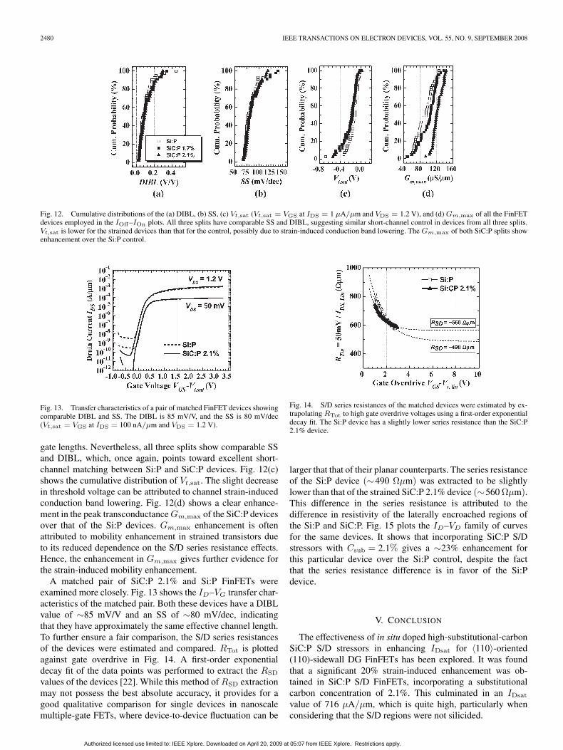
Fig. 12. Cumulative distributions of the (a) DIBL, (b) SS, (c) Vt,sat (Vt,sat = VGS at IDS = 1 µA/µm and VDS = 1.2 V), and (d) Gm,max of all the FinFETdevices employed in the IOff–IOn plots. All three splits have comparable SS and DIBL, suggesting similar short-channel control in devices from all three splits.Vt,sat is lower for the strained devices than that for the control, possibly due to strain-induced conduction band lowering. The Gm,max of both SiC:P splits showenhancement over the Si:P control.
Fig. 13. Transfer characteristics of a pair of matched FinFET devices showingcomparable DIBL and SS. The DIBL is 85 mV/V, and the SS is 80 mV/dec(Vt,sat = VGS at IDS = 100 nA/µm and VDS = 1.2 V).
gate lengths. Nevertheless, all three splits show comparable SSand DIBL, which, once again, points toward excellent short-channel matching between Si:P and SiC:P devices. Fig. 12(c)shows the cumulative distribution of Vt,sat. The slight decreasein threshold voltage can be attributed to channel strain-inducedconduction band lowering. Fig. 12(d) shows a clear enhance-ment in the peak transconductance Gm,max of the SiC:P devicesover that of the Si:P devices. Gm,max enhancement is oftenattributed to mobility enhancement in strained transistors dueto its reduced dependence on the S/D series resistance effects.Hence, the enhancement in Gm,max gives further evidence forthe strain-induced mobility enhancement.
A matched pair of SiC:P 2.1% and Si:P FinFETs wereexamined more closely. Fig. 13 shows the ID–VG transfer char-acteristics of the matched pair. Both these devices have a DIBLvalue of ∼85 mV/V and an SS of ∼80 mV/dec, indicatingthat they have approximately the same effective channel length.To further ensure a fair comparison, the S/D series resistancesof the devices were estimated and compared. RTot is plottedagainst gate overdrive in Fig. 14. A first-order exponentialdecay fit of the data points was performed to extract the RSD
values of the devices [22]. While this method of RSD extractionmay not possess the best absolute accuracy, it provides for agood qualitative comparison for single devices in nanoscalemultiple-gate FETs, where device-to-device fluctuation can be
Fig. 14. S/D series resistances of the matched devices were estimated by ex-trapolating RTot to high gate overdrive voltages using a first-order exponentialdecay fit. The Si:P device has a slightly lower series resistance than the SiC:P2.1% device.
larger that that of their planar counterparts. The series resistanceof the Si:P device (∼490 Ωµm) was extracted to be slightlylower than that of the strained SiC:P 2.1% device (∼560 Ωµm).This difference in the series resistance is attributed to thedifference in resistivity of the laterally encroached regions ofthe Si:P and SiC:P. Fig. 15 plots the ID–VD family of curvesfor the same devices. It shows that incorporating SiC:P S/Dstressors with Csub = 2.1% gives a ∼23% enhancement forthis particular device over the Si:P control, despite the factthat the series resistance difference is in favor of the Si:Pdevice.
V. CONCLUSION
The effectiveness of in situ doped high-substitutional-carbonSiC:P S/D stressors in enhancing IDsat for 〈110〉-oriented(110)-sidewall DG FinFETs has been explored. It was foundthat a significant 20% strain-induced enhancement was ob-tained in SiC:P S/D FinFETs, incorporating a substitutionalcarbon concentration of 2.1%. This culminated in an IDsat
value of 716 µA/µm, which is quite high, particularly whenconsidering that the S/D regions were not silicided.
Authorized licensed use limited to: IEEE Xplore. Downloaded on April 20, 2009 at 05:07 from IEEE Xplore. Restrictions apply.

LIOW et al.: STRAINED n-CHANNEL FinFETs FEATURING IN SITU DOPED SILICON–CARBON S/D STRESSORS 2481
Fig. 15. IDS–VDS curves showing 23% IDsat enhancement for this pair ofmatched devices (Vt,sat = VGS at IDS = 100 nA/µm and VDS = 1.2 V).This enhancement is mainly attributed to strain effects.
ACKNOWLEDGMENT
T.-Y. Liow would like to thank A*STAR for a GraduateScholarship Award. K.-M. Tan would like to thank the NationalUniversity of Singapore and Chartered Semiconductor Manu-facturing, Singapore, for a Graduate Scholarship Award.
REFERENCES
[1] K. W. Ang, K. J. Chui, V. Bliznetsov, A. Du, N. Balasubramanian,M. F. Li, G. S. Samudra, and Y.-C. Yeo, “Enhanced performance in 50 nmN-MOSFETs with silicon–carbon source/drain regions,” in IEDM Tech.Dig., 2004, pp. 1069–1071.
[2] K.-J. Chui, K.-W. Ang, N. Balasubramanian, M.-F. Li, G. Samudra, andY.-C. Yeo, “N-MOSFET with silicon–carbon source/drain for enhance-ment of carrier transport,” IEEE Trans. Electron Devices, vol. 54, no. 2,pp. 249–256, Feb. 2007.
[3] Y. Liu, O. Gluschenkov, J. Li, A. Madan, A. Ozcan, B. Kim, T. Dyer,A. Chakravarti, K. Chan, C. Lavoie, I. Popova, T. Pinto, N. Rovedo,Z. Luo, R. Loesing, W. Henson, and K. Rim, “Strained Si channelMOSFETs with embedded silicon carbon formed by solid phase epitaxy,”in VLSI Symp. Tech. Dig., 2007, pp. 44–45.
[4] K.-W. Ang, K.-J. Chui, C.-H. Tung, N. Balasubramanian, G. S. Samudra,and Y.-C. Yeo, “Performance enhancement in uniaxial strained silicon-on-insulator N-MOSFETs featuring silicon–carbon source/drain regions,”IEEE Trans. Electron Devices, vol. 54, no. 11, pp. 2910–2917, Nov. 2007.
[5] Y.-C. Yeo, “Enhancing CMOS transistor performance using lattice-mismatched materials in source/drain regions,” Semicond. Sci. Technol.,vol. 22, no. 1, pp. S177–S182, Jan. 2007.
[6] T.-Y. Liow, K.-M. Tan, R. T. P. Lee, A. Du, C.-H. Tung, G. S. Samudra,W.-J. Yoo, N. Balasubramanian, and Y.-C. Yeo, “Strained n-channelFinFETs with 25 nm gate length and silicon–carbon source/drainregions for performance enhancement,” in VLSI Symp. Tech. Dig., 2006,pp. 68–69.
[7] T.-Y. Liow, K.-M. Tan, R. T. P. Lee, C.-H. Tung, G. S. Samudra,N. Balasubramanian, and Y.-C. Yeo, “N-channel (110)-sidewall strainedFinFETs with silicon–carbon source and drain stressors and tensile cap-ping layer,” IEEE Electron Device Lett., vol. 28, no. 11, pp. 1014–1017,Nov. 2007.
[8] T.-Y. Liow, K.-M. Tan, H.-C. Chin, R. T. P. Lee, C.-H. Tung,G. S. Samudra, N. Balasubramanian, and Y.-C. Yeo, “Carrier trans-port characteristics of sub-30 nm strained n-channel FinFETs featuringsilicon–carbon source/drain regions and methods for further performanceenhancement,” in IEDM Tech. Dig., 2006, pp. 474–476.
[9] K.-W. Ang, K.-J. Chui, V. Bliznetsov, C.-H. Tung, A. Du,N. Balasubramanian, G. Samudra, M. F. Li, and Y.-C. Yeo, “Latticestrain analysis of transistor structures with silicon-germanium andsilicon–carbon source/drain stressors,” Appl. Phys. Lett., vol. 86, no. 9,p. 093 102, Feb. 2000.
[10] F. Durand and J. C. Duby, “Carbon solubility in solid and liquidsilicon—A review with reference to eutectic equilibrium,” J. Phase Equi-libria, vol. 20, no. 1, pp. 61–63, Jan. 1999.
[11] P. Werner, S. Eichler, and G. Mariani, “Investigation of CxSi defects inC implanted silicon by transmission electron microscopy,” Appl. Phys.Lett., vol. 70, no. 2, pp. 252–254, Jan. 1997.
[12] G. G. Fischer, P. Zaumseil, E. Bugiel, and H. J. Osten, “Investigation ofthe high temperature behavior of strained Si1−yCy/Si heterostructures,”J. Appl. Phys., vol. 77, no. 5, pp. 1934–1937, Mar. 1995.
[13] J. W. Strane, H. J. Stein, S. R. Lee, S. T. Picraux, J. K. Watanabe,and J. W. Mayer, “Precipitation and relaxation in strained Si1−yCy/Siheterostructures,” J. Appl. Phys., vol. 76, no. 6, pp. 3656–3668, Sep. 1994.
[14] T.-Y. Liow, K.-M. Tan, R. T. P. Lee, M. Zhu, K.-M. Hoe, G. S. Samudra,N. Balasubramanian, and Y.-C. Yeo, “Spacer removal technique forboosting strain in n-channel FinFETs with silicon–carbon source anddrain stressors,” IEEE Electron Device Lett., vol. 29, no. 1, pp. 80–82,Jan. 2008.
[15] E. Kasper, K.-J. Herzog, and H. Kibbel, “A one-dimensional SiGe super-lattice grown by UHV epitaxy,” Appl. Phys. A, Mater. Sci. Process., vol. 8,no. 3, pp. 199–205, Nov. 1975.
[16] R. People and J. C. Bean, “Calculation of critical layer thickness versuslattice mismatch for GexSi1−x/Si strained-layer heterostructures,” Appl.Phys. Lett., vol. 47, no. 3, pp. 322–324, Aug. 1985.
[17] M. Bauer, V. Machkaoutsan, and C. Arena, “Highly tensile strainedsilicon–carbon alloys epitaxially grown into recessed source drain areasof NMOS devices,” Semicond. Sci. Technol., vol. 22, no. 1, pp. 183–187,Jan. 2007.
[18] M. Bauer, D. Weeks, Y. Zhang, and V. Machkaoutsan, “Tensile strainedselective silicon carbon alloys for recessed source drain areas of devices,”Electrochem. Soc. Trans., vol. 3, no. 7, pp. 187–196, 2006.
[19] J. Kedzierski, M. Ieong, E. Nowak, T. S. Kanarsky, Y. Zhang, R. Roy,D. Boyd, and D. Fried, “Extension and source/drain design for high-performance FinFET devices,” IEEE Trans. Electron Devices, vol. 50,no. 4, pp. 952–958, Apr. 2003.
[20] T.-Y. Liow, R. T. P. Lee, K.-M. Tan, M. Zhu, K.-M. Hoe,G. S. Samudra, N. Balasubramanian, and Y.-C. Yeo, “Strained n-channelFinFETs with high-stress nickel silicide-carbon contacts and integrationwith FUSI metal gate technology,” in Proc. Ext. Abstr. Int. Conf. SolidState Devices Mater., Ibaraki, Japan, Sep. 18-21, 2007.
[21] R. T. P. Lee, L.-T. Yang, T.-Y. Liow, K.-M. Tan, A. E.-J. Lim, K.-W. Ang,D. M. Y. Lai, K. M. Hoe, G.-Q. Lo, G. S. Samudra, D. Z. Chi, andY.-C. Yeo, “Nickel-silicide: Carbon contact technology for n-channelMOSFETs with silicon–carbon source/drain,” IEEE Electron DeviceLett., vol. 29, no. 1, pp. 89–92, Jan. 2008.
[22] A. Dixit, A. Kottantharayil, N. Collaert, M. Goodwin, M. Jurczak, andK. De Meyer, “Analysis of the parasitic S/D resistance in multiple-gateFETs,” IEEE Trans. Electron Devices, vol. 52, no. 6, pp. 1132–1140,Jun. 2005.
Tsung-Yang Liow (S’06) received the B.Eng. de-gree in electrical and computer engineering from theNational University of Singapore (NUS), Singapore,in 2003. He is currently working toward the Ph.D.degree in electrical and computer engineering inthe Silicon Nano Device Laboratory, Department ofElectrical and Computer Engineering, NUS.
He is with the Institute of Microelectronics,Agency for Science, Technology, and Research(A*STAR), Singapore. His research interests includethe design and fabrication of sub-10-nm multiple-
gate FDSOI and nanowire transistors, as well as performance enhancementtechniques, such as channel strain engineering.
Mr. Liow was the recipient of the NUS Faculty of Engineering InnovationAward in 2003 and the A*STAR Graduate Scholarship from 2004 to 2007.
Authorized licensed use limited to: IEEE Xplore. Downloaded on April 20, 2009 at 05:07 from IEEE Xplore. Restrictions apply.

2482 IEEE TRANSACTIONS ON ELECTRON DEVICES, VOL. 55, NO. 9, SEPTEMBER 2008
Kian-Ming Tan received the B.Eng. (with first-classhonors) and M.Eng. degrees in electrical engineeringfrom the National University of Singapore (NUS),Singapore. He is currently working toward the Ph.D.degree in electrical engineering in the Silicon NanoDevice Laboratory, Department of Electrical andComputer Engineering, NUS.
His research interests include plasma etching tech-nologies, strained Si devices, and multiple-gate tran-sistor fabrication.
Doran Weeks received the M.S. degree in materialsscience and engineering from Arizona State Univer-sity, Phoenix, in December 1999.
He is currently a Staff Process Engineer with ASMAmerica Inc., Phoenix. His expertise is in the fieldof Si-based epitaxy, having done development on awide range of applications from SiGe HBTs, CMOSepitaxial source/drain stressors, MEMS, and siliconon sapphire.
Rinus Tek Po Lee (S’06) received the B.Eng. de-gree in electrical engineering and the M.Sc. degreein applied physics from the National University ofSingapore (NUS), Singapore. He is currently work-ing toward the Ph.D. degree in electrical engineering,with research work on parasitic resistance scaling inmultiple-gate transistors with Prof. Y.-C. Yeo, in theSilicon Nano Device Laboratory (SNDL), Depart-ment of Electrical and Computer Engineering, NUS.
He was with the Institute of Materials Researchand Engineering, Agency of Science Technology and
Research, Singapore, where he worked on the development of advanced processtechnologies for contact metallization. Since 2005, he has been with the SNDL.His current research interests include device physics and process technologyintegration for the multiple-gate transistor architecture.
Mr. Lee was the recipient of the Marubun Research Promotion FoundationGrant for the 2006 Solid State Devices and Materials Conference, Yokohama,and the Gold Award at the 2007 Taiwan Semiconductor Manufacturing Com-pany Outstanding Student Research Award.
Ming Zhu received the B.S. degree in physics fromWuhan University, Wuhan, China, in 2000 and thePh.D. degree in microelectronics from Shanghai In-stitute of Microsystem and Information Technology,Chinese Academy of Sciences, Shanghai, China,in 2005.
From 2005 to 2008, he was a Research Fellowwith the Silicon Nano Device Laboratory, Depart-ment of Electrical and Computer Engineering, Na-tional University of Singapore, Singapore, where heworked on high-mobility transistor fabrication. He is
currently with the Technology Development Department, Chartered Semicon-ductor Manufacturing, Singapore.
Keat-Mun Hoe received the B.Eng. degree (Hon-ours) in electronics and electrical engineering fromthe University of Birmingham, Birmingham, U.K.,in 2005.
He is currently with Wong’s Kong King Interna-tional (Holdings) Ltd. He was with the Institute ofMicroelectronics (IME), Agency of Science Tech-nology and Research, Singapore, where he trainedin the analytical prospect of the TEM under thetutelage of T. C. Hang. Upon embarking on thisnew expertise, he has done many analytical studies
using TEM to help researchers and students in their research papers. With theexperience provided by IME, he has now gone on to pursue a career in salesand application engineering.
Chih-Hang Tung (M’01–SM’02) received theM.Sc. degree from Illinois Institute of Technology,Chicago, in 1987.
He is with the Institute of Microelectronics,A*STAR, Singapore. He is the author of more than180 journal/conference proceeding papers and thebook ULSI Semiconductor Technology Atlas (Wiley-IEEE, 2003). His research interests include the ap-plication of TEM in semiconductor materials, deviceand process characterization, DRAM and SRAMreliability and FA, and physical characterization of
nanodevice and products.Mr. Tung is an EDS Distinguished Lecturer and a Guest Editor for the IEEE
TRANSACTIONS ON DEVICE AND MATERIALS RELIABILITY. He was theIPFA 2006 Technical Chair and 2007 Co-General Chair and is the 2008 GeneralChair.
Matthias Bauer received the Ph.D. degree from the University of Stuttgart,Stuttgart, Germany, in 2001.
Since 2001, he has been with ASM America Inc., Phoenix, AZ, where heis currently a Senior Staff Process Engineer. He is author or coauthor of over30 technical articles and is the holder of three patents. His main focus is thedevelopment of novel epitaxy processes, using new precursors, enabling newapplications. Among these epitaxial technologies are selective SiGe and SiCfor CMOS epitaxial source/drain stressors, pure Ge on silicon, and thin strainrelaxed SiGe buffer layers for lattice engineered films.
Jennifer Spear received the B.S. degree in materi-als science and engineering from the University ofPittsburgh, Pittsburgh, PA, and the M.S. degree inmaterials science and engineering, and business fromArizona State University, Phoenix.
She was previously with Philips Analytical andTechnos International. She is currently with ASMAmerica Inc., Phoenix. Her research interest is inmetrology.
Shawn G. Thomas (S’93–M’99) received theB.S.E.E. degree from the University of Illinois atUrbana-Champaign in 1993, and the M.S. and Ph.D.(in 1999) degrees in the area of SiGe materials anddevices from the University of California at LosAngeles.
From 1999 to 2006, he was with Motorola, wherehe was engaged in the research and development ofSiGe HBTs, strained Si and strained SiGe MOSFETtechnologies, and the application of carbon nano-tubes in field emission displays, logic transistors and
passive devices. Additionally, he has worked on pure Ge on Si for CMOS-integrated photodetectors, MOSFETs, and as a platform for the heterointegra-tion of III-V materials on a silicon substrate. He is currently the Director ofR&D for epitaxial technologies with ASM America Inc., Phoenix, AZ. Heauthored or coauthored more than 60 technical publications.
Ganesh S. Samudra received the Ph.D. degree fromPurdue University, West Lafayette, IN, in 1985.
He is currently an Associate Professor with theSilicon Nano Device Laboratory (SNDL), Depart-ment of Electrical and Computer Engineering, Na-tional University of Singapore (NUS), Singapore,where he has taught for about 15 year and ismostly involved in research projects on simulationand novel devices. He was a Visiting Professor withMassachusetts Institute of Technology, Cambridge,in 2001. He was with Texas Instruments (TI), Dallas,
for three years, before joining NUS. In TI, he worked on the developmentof technology computer-aided design tools linking device and circuit simu-lators and defining 3-D structures for simulation. He is the author of about120 technical papers in journals and conference proceedings.
Authorized licensed use limited to: IEEE Xplore. Downloaded on April 20, 2009 at 05:07 from IEEE Xplore. Restrictions apply.

LIOW et al.: STRAINED n-CHANNEL FinFETs FEATURING IN SITU DOPED SILICON–CARBON S/D STRESSORS 2483
N. Balasubramanian received the Ph.D. degree inphysics from Indian Institute of Technology, Madras,India, in 1990.
He was an Engineering Section Manager forCMOS front-end technologies with CharteredSemiconductor Manufacturing Ltd., Singapore. In1998, he joined the Institute of Microelectronics,Singapore, where he held various positions as Mem-ber of Technical Staff, Senior Technical Manager,and Lab Director for Semiconductor ProcessTechnology and as the Director for Bioelectronics
and BioMEMS Program. Since April 2008, he has been with Silterra Malaysia,Kulim, Malaysia, as a Fellow for Technology Development. He has more than17 years of experience in the IC industry under different capacities in researchand development, process module operations, technology development,and program management. He is the author or coauthor of more than90 publications in peer-reviewed journals on research topics covering Sinanowire nanoelectronics and biosensor devices, CMOS devices, CMOSfront-end technologies, and heterogeneous integration. He is also the holder ofeight U.S. patents.
Yee-Chia Yeo received the B.Eng. (first-classhonors) and M.Eng. degrees in electrical engineeringfrom the National University of Singapore (NUS),Singapore, and the M.S. and Ph.D. degrees in elec-trical engineering and computer sciences from theUniversity of California, Berkeley.
He had worked on optoelectronic devices at theBritish Telecommunications Laboratories, U.K., andon CMOS technology at the University of California,Berkeley. In 2001 to 2003, he was with TaiwanSemiconductor Manufacturing Company (TSMC),
where he worked on exploratory transistor technologies. He is currently anAssistant Professor of electrical and computer engineering with the SiliconNano Device Laboratory, Department of Electrical and Computer Engineering,NUS, where he leads research efforts in strained transistor technologies andsub-30-nm device work. He is also currently a Research Program Managerwith the Agency for Science, Technology, and Research (A*STAR), Singapore,where he manages the Nanoelectronics Research Program. He is the author orcoauthor of more than 260 journal and conference proceeding papers, and abook chapter. He is also the holder of 71 U.S. patents.
Dr. Yeo served on the IEDM Sub-Committee on CMOS Devices from 2005to 2006. He was the recipient of the 1995 IEE Prize from the Institution ofElectrical Engineers, U.K., the 1996 Lee Kuan Yew Gold Medal, the 1996Institution of Engineers Singapore Gold Medal, 1997–2001 NUS OverseasGraduate Scholarship Award, the 2001 IEEE Electron Devices Society Grad-uate Student Fellowship Award, the 2002 IEEE Paul Rappaport Award, and2003 TSMC Invention Awards, the 2006 Singapore Young Scientist Award, the2006 Singapore Youth Award in Science and Technology, the 2008 NationalResearch Foundation Fellowship, and the 2008 NUS Young Researcher Award.
Authorized licensed use limited to: IEEE Xplore. Downloaded on April 20, 2009 at 05:07 from IEEE Xplore. Restrictions apply.