High-sensitivity 10 Gbps Ge-on-Si photoreceiver operating at λ ~155 μm
Upload
independentCategory
view
2download
0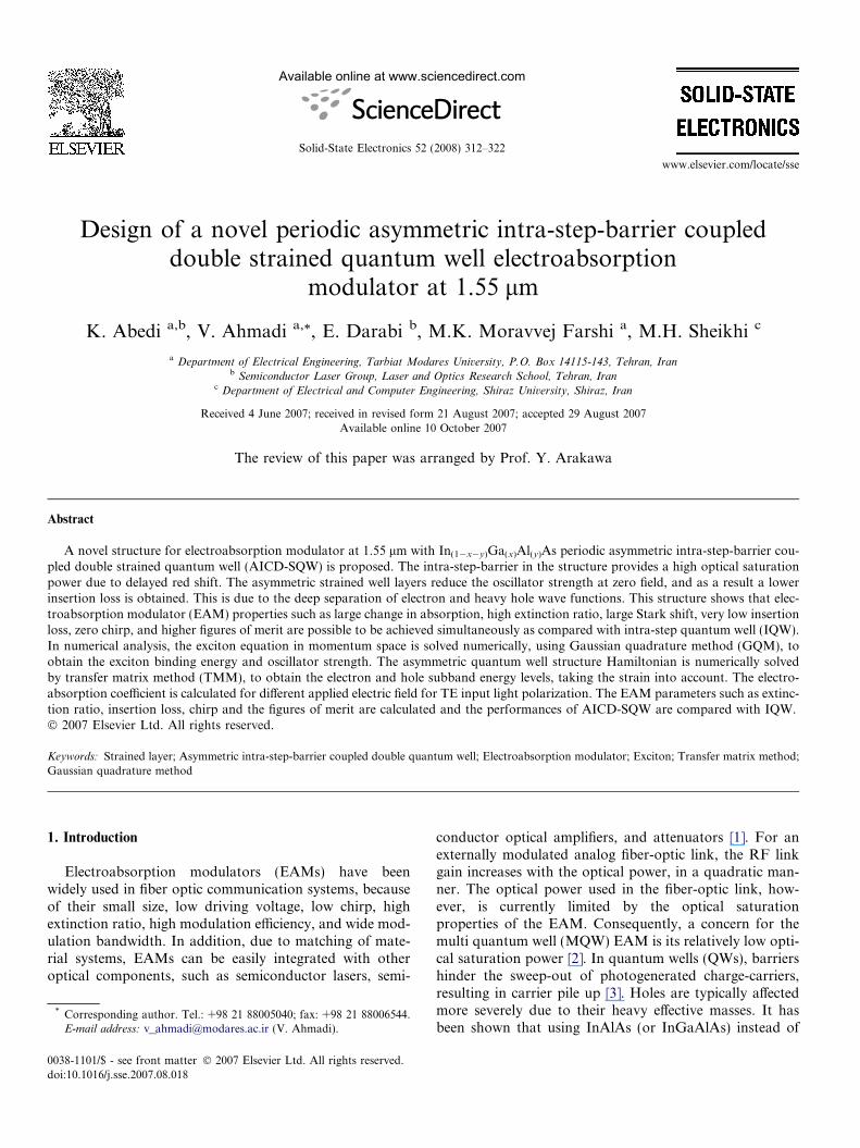
Available online at www.sciencedirect.com
www.elsevier.com/locate/sse
Solid-State Electronics 52 (2008) 312–322
Design of a novel periodic asymmetric intra-step-barrier coupleddouble strained quantum well electroabsorption
modulator at 1.55 lm
K. Abedi a,b, V. Ahmadi a,*, E. Darabi b, M.K. Moravvej Farshi a, M.H. Sheikhi c
a Department of Electrical Engineering, Tarbiat Modares University, P.O. Box 14115-143, Tehran, Iranb Semiconductor Laser Group, Laser and Optics Research School, Tehran, Iran
c Department of Electrical and Computer Engineering, Shiraz University, Shiraz, Iran
Received 4 June 2007; received in revised form 21 August 2007; accepted 29 August 2007Available online 10 October 2007
The review of this paper was arranged by Prof. Y. Arakawa
Abstract
A novel structure for electroabsorption modulator at 1.55 lm with In(1�x�y)Ga(x)Al(y)As periodic asymmetric intra-step-barrier cou-pled double strained quantum well (AICD-SQW) is proposed. The intra-step-barrier in the structure provides a high optical saturationpower due to delayed red shift. The asymmetric strained well layers reduce the oscillator strength at zero field, and as a result a lowerinsertion loss is obtained. This is due to the deep separation of electron and heavy hole wave functions. This structure shows that elec-troabsorption modulator (EAM) properties such as large change in absorption, high extinction ratio, large Stark shift, very low insertionloss, zero chirp, and higher figures of merit are possible to be achieved simultaneously as compared with intra-step quantum well (IQW).In numerical analysis, the exciton equation in momentum space is solved numerically, using Gaussian quadrature method (GQM), toobtain the exciton binding energy and oscillator strength. The asymmetric quantum well structure Hamiltonian is numerically solvedby transfer matrix method (TMM), to obtain the electron and hole subband energy levels, taking the strain into account. The electro-absorption coefficient is calculated for different applied electric field for TE input light polarization. The EAM parameters such as extinc-tion ratio, insertion loss, chirp and the figures of merit are calculated and the performances of AICD-SQW are compared with IQW.� 2007 Elsevier Ltd. All rights reserved.
Keywords: Strained layer; Asymmetric intra-step-barrier coupled double quantum well; Electroabsorption modulator; Exciton; Transfer matrix method;Gaussian quadrature method
1. Introduction
Electroabsorption modulators (EAMs) have beenwidely used in fiber optic communication systems, becauseof their small size, low driving voltage, low chirp, highextinction ratio, high modulation efficiency, and wide mod-ulation bandwidth. In addition, due to matching of mate-rial systems, EAMs can be easily integrated with otheroptical components, such as semiconductor lasers, semi-
0038-1101/$ - see front matter � 2007 Elsevier Ltd. All rights reserved.
doi:10.1016/j.sse.2007.08.018
* Corresponding author. Tel.: +98 21 88005040; fax: +98 21 88006544.E-mail address: [email protected] (V. Ahmadi).
conductor optical amplifiers, and attenuators [1]. For anexternally modulated analog fiber-optic link, the RF linkgain increases with the optical power, in a quadratic man-ner. The optical power used in the fiber-optic link, how-ever, is currently limited by the optical saturationproperties of the EAM. Consequently, a concern for themulti quantum well (MQW) EAM is its relatively low opti-cal saturation power [2]. In quantum wells (QWs), barriershinder the sweep-out of photogenerated charge-carriers,resulting in carrier pile up [3]. Holes are typically affectedmore severely due to their heavy effective masses. It hasbeen shown that using InAlAs (or InGaAlAs) instead of
K. Abedi et al. / Solid-State Electronics 52 (2008) 312–322 313
InP or InGaAsP as barrier materials improves the opticalsaturation of the MQW EAM, effectively as a result ofthe reduced valence band offset. It has also been reportedthat the strain-compensated InGaAsP/InGaAsP [4] andInAsP/GaInP [5], which have shallow wells, improves thesaturation optical power at 1.3 and 1.55 lm, respectively.Recently, the use of an asymmetric QW with a step barrierto achieve high-optical-power operation has been proposed[6,7]. The intra-step quantum well (IQW) was shown todelay the onset of the red shift of the QCSE to a higherelectric field, when the electric field was applied from thewell to the step barrier. Due to the delayed red shift, theoperation voltage of the EAM with IQWs was increased.Since at higher fields, the carrier escape time becomes smal-ler, the charge screening effect due to the trapped chargecarriers is reduced [3]. IQW, however, has the disadvantageof high insertion (propagation) loss.
In this paper, to reduce the insertion loss and improvethe performance of the high power EAM with IQW, wepropose an asymmetric intra-step-barrier coupled doublestrained quantum well (AICD-SQW) structure. In thisstructure, we adopt the approach that oscillator strength,which is proportional to the square of the spatial overlapintegral between the electron and the hole envelope wavefunctions, reduces at zero field.
Considering the new proposed structure, a numericalmodel is developed, to analyze the effect of strain on theelectroabsorption modulator parameters. We have com-pared the results obtained from all three structures,AICD-SQW, AICD-QW and IQW, with each other, forthe first time. First, the electron and hole subband energylevels and their envelope wave functions are calculatedusing transfer matrix method (TMM) considering finitebarrier, strain effect and applied electric field [8]. Then,the optical matrix elements of the structures for TE andTM polarization are calculated. The exciton equation inmomentum space is solved numerically using the Gaussianquadrature method (GQM) [9,10] to obtain the excitonbinding energy and oscillator strength. The electroabsorp-tion coefficient is calculated for different applied electricfield for TE input light polarization. Finally, the EAMparameters such as extinction ratio, insertion loss, chirpand the figures of merit [11] are calculated and the perfor-mances of AICD-SQW, AICD-QW and IQW structuresare compared together. It is shown the proposed AICD-SQW structure has large change in absorption, high extinc-tion ratio, large Stark shift, very low insertion loss, zerochirp and higher figures of merit as compared with IQW.
The organization of this paper is as follows: In Section 2,details of the modulator active layer with AICD-SQWstructures are described and design procedure is discussedin terms of the band line-up and the strain applied to thewell layers. In Section 3, the theory behind our analysis isdiscussed, and the numerical model of the electroabsorptionspectrum including the exciton peak, EAM characteristicssuch as extinction ratio, insertion loss, chirp and figuresof merit is presented. In Section 4, wave functions for elec-
tron (C1) and heavy hole (HH1), oscillator strength, transi-tion energy shift, and the modulator characteristics in IQW,AICD-QW, and AICD-SQW structures are numericallycalculated, using TMM and GQM. Comparison of theresults obtained for all three structures and the discussionfor designing a large change in absorption, high extinctionratio, very low insertion loss, and zero chirp close this sec-tion. Finally, conclusions are given in Section 5.
2. The electroabsorption modulator structure
In IQW structure, step barrier inside the well on the p-side of p–i–n structure suppresses the onset of the red shiftin quantum-confined Stark effect (QCSE) to a higher elec-tric field. Consequently, the optical saturation power isenhanced. However, due to the large effective mass differ-ence between the electron and the heavy hole, the heavyhole is mostly confined in the well region and the electronis uniformly distributed over the well and step-barrierregion at zero field [7]. Therefore, the oscillator strength,which is proportional to the square of the spatial overlapintegral between the electron and the hole envelope wavefunctions, and insertion loss will be large. To reduce theinsertion loss, we need to separate electron and heavy holewave functions at zero electric field. Here, we propose anovel asymmetric intra-step-barrier coupled doublestrained QW (AICD-SQW) structure with the conductionband profile shown in Fig. 1a. An asymmetric coupled dou-bled quantum well is inserted inside the well of IQW struc-ture as shown in the figure. If asymmetric wells are made ofthe same materials, the electron and heavy hole wave func-tions are mostly localized in the wide well which results inreduction of the insertion loss at zero electric field. Formore reduction, we apply compressive strain to the narrowwell and tensile strain to the wide well. As a result, the elec-tron and heavy hole are separated greatly. Thus, the inser-tion loss reduces further.
In this structure as shown in Fig. 1b, active region con-sists of an intrinsic eight-period AICD-SQW, separatedwith 100 A thick In0.52Al0.48As barriers, which are lattice-matched to InP. Each period of the proposed AICD-SQW consists of a 40 A thick In0.53Ga0.33Al0.14Asintra-step-barrier, a 15 A thick In0.52Al0.48As as the narrowbarrier, a 68 A thick In0.525Ga0.475As (%0.05 tensile strain)for the left well and a 35 A thick In0.608Ga0.392As (%0.52compressive strain) for the right well. The modulatorlength and optical confinement factor are taken to be200 lm and 0.15, respectively.
The given strain values above, have been chosen as thebest results obtained among several AICD-SQW structureswith various strain values under investigation. For the sakeof comparison, the calculated results for proposed AICD-SQW and AICD-QW structures are presented. It is notice-able that the left and the right wells materials in the latterstructure are assumed unstrained (In0.53Ga0.47As).
As a reference, we consider an IQW structure consistingof a 70 A thick In0.53Ga0.47As unstrained well and a 40 A

Fig. 1. (a) Conduction band profile of the proposed AICD-SQW and (b) cross-sectional layer structure of the EAM.
314 K. Abedi et al. / Solid-State Electronics 52 (2008) 312–322
thick In0.53Ga0.33Al0.14As unstrained intra-step-barrier. Itshould be noted that the well thicknesses of IQW andAICD-QW are theoretically set to have the same excitonpeak at �1.51 lm, for zero electric field.
3. Theory of the analysis
Calculation of absorption spectra is the basis of our the-oretical analysis. The field-dependent absorption spectrumand electroabsorption parameters such as extinction ratio,insertion loss, chirp and the figures of merit of theIn(1�x�y)Ga(x)Al(y)As AICD-SQW structures of Fig. 1 arecalculated by the following procedure. The subbands andthe envelope functions of electrons, heavy holes, and lightholes are calculated using TMM. Conduction and valencebands are assumed parabolic in our calculations. The con-duction band Hamiltonian is given by [8]
HC ¼�h2
2m�eðk2
x þ k2y þ k2
z Þ þ C1ðexx þ eyy þ ezzÞ þ V 0ðzÞ ð1Þ
H eðzÞ ¼ ��h2
2
o
oz1
m�eðzÞo
oz
� �þ V eðzÞ ð2Þ
E ¼ Et þ Een ¼
�h2ðk2x þ k2
yÞ2m�e
þ Een ð3Þ
where, z is the growth direction, �h is the reduced Planckconstant, m�e is the electron effective mass, C1 is the defor-mation potential for the conduction band, V0(z) is theheight of quantum well, Ve(z) is the quantum well confiningpotential in growth direction (z) for the electron, and Ee
n isthe Schrodinger equation eigenvalue. The effects of strainare calculated in the following way. The strain in the planeof the epitaxial growth is
e ¼ exx ¼ eyy ¼a0 � a
a0
ð4Þ
where a is the lattice constant of the quaternary epitaxiallayer and a0 is the lattice constant of the substrate, InP.The strain in the perpendicular direction can be expressedas
K. Abedi et al. / Solid-State Electronics 52 (2008) 312–322 315
ezz ¼ �2C12
C11
e ð5aÞ
exy ¼ exz ¼ ezy ¼ 0 ð5bÞ
where C11 and C12 are the elastic stiffness constants. Thestrain shift in the conduction band is determined by [8]
dEcðx; yÞ ¼ acðexx þ eyy þ ezzÞ ¼ 2ac 1� C12
C11
� �e ð6Þ
and the strain shifts for light and heavy holes in the valencebands are determined by
dEhhðx; yÞ ¼ �P e � Qe ð7aÞdElhðx; yÞ ¼ �P e þ Qe ð7bÞ
where
P e ¼ �avðexx þ eyy þ ezzÞ ¼ �2av 1� C12
C11
� �e ð8aÞ
Qe ¼ �b2ðexx þ eyy � 2ezzÞ ¼ �2b 1þ 2
C12
C11
� �e ð8bÞ
In Eq. (8) ac and av are the conduction band and valenceband hydrostatic deformation potentials, and b is thevalence band shear deformation potential. To obtain mostparameters for the In(1�x�y)Ga(x)Al(y) As material systems,a linear interpolation between the parameters of the rele-vant binary semiconductors is used. The material parame-ters of the binary semiconductors can be found in Table 1.For In(1�x�y)Ga(x)Al(y) As material system, the unstrainedbandgap is given as
Egðx; yÞ ¼ 0:36þ 2:093y þ 0:629xþ 0:577y2 þ 0:436x2
þ 1:013xy � 2:0xyð1� x� yÞ ðeVÞ ð9Þ
Thus, for the conduction and the valence subbands, thestrained quantum well potentials are determined by
V eðzÞ ¼dEc ¼ 2ac 1� C12
C11
h ie jzj 6 Lz
V 0 ¼ DEc ¼ QeDEg jzj > Lz
(ð10Þ
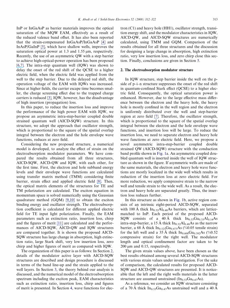
Table 1Parameters used in the calculation [12,13]
Parameters Symbol (unit)
Lattice constant a (A)Elastic stiffness constant C11 (1011 dyn/cm2)
C12 (1011 dyn/cm2)Hydrostatic deformation potentialFor conduction band ac (eV)For valence band av (eV)Shear deformation potential for valence band b (eV)Luttinger parameters c1
c2
c3
Electron effective mass me/m0
Heavy-hole effective mass mhh/m0
Conduction band position EHc ðeVÞ
Valence band position (Harrison’s model) EHv ðeVÞ
V hðzÞ ¼dEhhðlhÞ ¼ 2av 1� C12
C11
h ie� 2b 1þ 2 C2
C11
� �e jzj 6 Lz
V 0 ¼ DEhhðlhÞ ¼ QhhðlhÞDEg jzj > Lz
8<:
ð11Þ
where DEg is the difference in the bulk bandgap betweenwell and barrier, Lz is the well width, and Qe, Qhh, andQlh are band offsets using Harrison’s model [12,13].
The strained bandgaps can then be expressed as
Ec�hhðx; yÞ ¼ Egðx; yÞ þ dEcðx; yÞ � dEhhðx; yÞ ð12aÞEc�lhðx; yÞ ¼ Egðx; yÞ þ dEcðx; yÞ � dElhðx; yÞ ð12bÞ
3.1. Electroabsorption spectrum
The electroabsorption spectrum a(hm) is related to theimaginary part of the dielectric constant, ei(hm), given as[14]
aðhmÞ ¼ 2pk0nr
eiðhmÞ ¼ xcnr
eiðhmÞ ð13Þ
where k0, c, and nr are the free-space wavelength of incidentlight, the speed of light in vacuum, and the refractive index,respectively. a(hm) in (13) can be defined as
aðhmÞ ¼ aðhmÞband þ aðhmÞexciton ð14Þ
The first term is due to the band-to-band transitions andthe second term is due to the excitonic transitions. The elec-troabsorption coefficient of the band-to-band transitionsbetween nth electron subband and mth hole subband iswritten as
aðhmÞband ¼ e2
e0m20cnrxLz
:l
�h2
ZM2
nmðEÞLðhm� E � Eg
� Een � Eh
mÞdE ð15Þ
where e0 is the dielectric constant, m0 the free-electronmass, nr the refractive index, Lz the effective thickness ofthe AICD-SQW, Eg the energy gap, l the reduced massfor the motion in the xy plane, and L(y) the line shape
GaAs InAs InP AlAs
5.6533 6.0584 5.8688 5.66011.879 8.329 10.11 12.55.376 4.526 5.61 5.34
�7.17 �5.08 �5.04 �5.641.16 1.00 1.27 2.47�1.7 �1.8 �1.7 �1.5
6.8 20.4 4.95 3.451.9 8.3 1.65 0.682.73 9.1 2.35 1.290.067 0.023 0.077 0.150.5 0.40 0.60 0.791.53 0.801 1.35 2.52550.111 0.441 0.00 �0.4245

316 K. Abedi et al. / Solid-State Electronics 52 (2008) 312–322
function for each transition, respectively. Also, since thelayer thicknesses in consideration are small compared tothe light wavelengths, the dielectric constant of theAICD-SQW material can be calculated in an effective med-ium [15] approach by weighing the respective constants forwells and barriers materials with their relative thicknesses.
Fig. 2. Envelop wave functions for the first electron in (a) IQW, (c) AICD-QWand (f) AICD-SQW structures at electric fields of 0, 60 and 120 kV/cm.
The total dielectric function eAICD-SQW and the refractiveindex of AICD-SQW, nr are given by
eAICDSQW ¼Lsb � esb þ Llw � elw þ Lnb � enb þ Lrw � erw
Lsb þ Llw þ Lnb þ Lrw
ð16Þ
and (e) AICD-SQW and the first heavy hole in (b) IQW, (d) AICD-QW
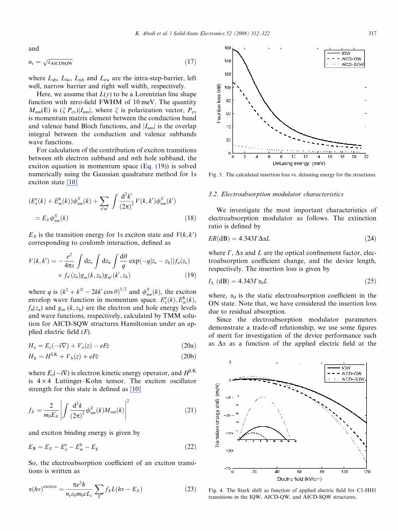
Fig. 3. The calculated insertion loss vs. detuning energy for the structures.
Fig. 4. The Stark shift as function of applied electric field for C1-HH1transitions in the IQW, AICD-QW, and AICD-SQW structures.
K. Abedi et al. / Solid-State Electronics 52 (2008) 312–322 317
and
nr ¼ffiffiffiffiffiffiffiffiffiffiffiffiffiffiffiffiffiffieAICDSQWp ð17Þ
where Lsb, Llw, Lnb and Lrw are the intra-step-barrier, leftwell, narrow barrier and right well width, respectively.
Here, we assume that L(y) to be a Lorentzian line shapefunction with zero-field FWHM of 10 meV. The quantityMnm(E) is (nÆPcv)jInmj, where n is polarization vector, Pcv
is momentum matrix element between the conduction bandand valence band Bloch functions, and jInmj is the overlapintegral between the conduction and valence subbandswave functions.
For calculation of the contribution of exciton transitionsbetween nth electron subband and mth hole subband, theexciton equation in momentum space (Eq. (19)) is solvednumerically using the Gaussian quadrature method for 1sexciton state [10]
ðEenðkÞ þ Eh
mðkÞÞ/XnmðkÞ þ
Xn0m0
Zd2k0
ð2pÞ2V ðk; k0Þ/X
nmðk0Þ
¼ EX /XnmðkÞ ð18Þ
EX is the transition energy for 1s exciton state and V(k,k 0)corresponding to coulomb interaction, defined as
V ðk; k0Þ ¼ � e2
4pe
Zdze
Zdzh
Zdhq
expð�qjze � zhjÞfnðzeÞ
� fn0 ðzeÞgmðk; zhÞgm0 ðk0; zhÞ ð19Þ
where q is ðk2 þ k02 � 2kk0 cos hÞ1=2 and /XnmðkÞ, the exciton
envelop wave function in momentum space. EenðkÞ;Eh
mðkÞ,fn(ze) and gm (k,zh) are the electron and hole energy levelsand wave functions, respectively, calculated by TMM solu-tion for AICD-SQW structures Hamiltonian under an ap-plied electric field (F).
H e ¼ Ecð�irÞ þ V eðzÞ � eFz ð20aÞH h ¼ HLK þ V hðzÞ þ eFz ð20bÞ
where Ec(�i$) is electron kinetic energy operator, and HLK
is 4 · 4 Luttinger–Kohn tensor. The exciton oscillatorstrength for this state is defined as [10]
fX ¼2
m0EX
Zd2k
ð2pÞ2/X
nmðkÞMnmðkÞ�����
�����2
ð21Þ
and exciton binding energy is given by
EB ¼ EX � Een � Eh
m � Eg ð22Þ
So, the electroabsorption coefficient of an exciton transi-tions is written as
aðhmÞexciton ¼ pe2�hnre0m0cLz
XX
fX Lðhm� EX Þ ð23Þ
3.2. Electroabsorption modulator characteristics
We investigate the most important characteristics ofelectroabsorption modulator as follows. The extinctionratio is defined by
ERðdBÞ ¼ 4:343CDaL ð24Þ
where C, Da and L are the optical confinement factor, elec-troabsorption coefficient change, and the device length,respectively. The insertion loss is given by
IL ðdBÞ ¼ 4:343Ca0L ð25Þ
where, a0 is the static electroabsorption coefficient in theON state. Note that, we have considered the insertion lossdue to residual absorption.
Since the electroabsorption modulator parametersdemonstrate a trade-off relationship, we use some figuresof merit for investigation of the device performance suchas Da as a function of the applied electric field at the
318 K. Abedi et al. / Solid-State Electronics 52 (2008) 312–322
operation wavelength, and Da/a0 as a function of detuningenergy [11]. Da/a0 determines the minimum achievableinsertion loss (due to the static material absorption) for agiven extinction ratio. The larger the Da/a0 is, the smallerwill be the insertion loss, because the insertion (residual)loss is proportional to a0 and the extinction ratio is propor-tional to Da.
The last parameter that characterizes an optical commu-nication system is its chirp. The amount of chirp is deter-mined by the chirp parameter given by, aH = (4p/k)(Dn/Da) [16], where Dn is the refractive index change producedby a change in absorption coefficient, Da, and k is the oper-ation wavelength. Da and Dn are related together throughthe Kramers–Kronig relations.
4. Numerical results and discussion
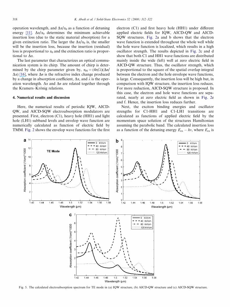
Here, the numerical results of periodic IQW, AICD-QW, and AICD-SQW electroabsorption modulators arepresented. First, electron (C1), heavy hole (HH1) and lighthole (LH1) subband levels and envelop wave function arenumerically calculated as function of electric field byTMM. Fig. 2 shows the envelop wave functions for the first
Fig. 5. The calculated electroabsorption spectrum for TE mode in (a) IQ
electron (C1) and first heavy hole (HH1) under differentapplied electric fields for IQW, AICD-QW and AICD-SQW structures. Fig. 2a and b shows that the electronwave function is extended throughout the whole well whilethe hole wave function is localized, which results in a highoscillator strength. The results depicted in Fig. 2c and dshow that both C1 and HH1 wave functions are distributedmainly inside the wide (left) well at zero electric field inAICD-QW structure. Thus, the oscillator strength, whichis proportional to the square of the spatial overlap integralbetween the electron and the hole envelope wave functions,is large. Consequently, the insertion loss will be high but, incomparison with IQW structure, the insertion loss reduces.For more reduction, AICD-SQW structure is proposed. Inthis case, the electron and hole wave functions are sepa-rated, nearly at zero electric field as shown in Fig. 2eand f. Hence, the insertion loss reduces further.
Next, the exciton binding energies and oscillatorstrengths for C1-HH1 and C1-LH1 transitions arecalculated as functions of applied electric field by themomentum space solution of the structures Hamiltonianassuming the parabolic band. The calculated insertion lossas a function of the detuning energy Eex � hm, where Eex is
W structure, (b) AICD-QW structure and (c) AICD-SQW structure.
K. Abedi et al. / Solid-State Electronics 52 (2008) 312–322 319
the exciton resonance energy, is shown in Fig. 3. The valuesof insertion loss are 11.31, 7.54, and 1.77 dB at the detun-ing energy of 21 meV corresponding to 1.55 lm, respec-tively. The results in Fig. 3 demonstrate that, indeed,greatly decreased insertion loss can be obtained by apply-ing AICD-SQW structure.
When the electric field is applied from the narrow well tothe step barrier direction, the electron sees narrow barrier(15 A) while the hole sees the step barrier. So the electronis shifted effectively while the hole is blocked by the stepbarrier. To overcome the step barrier, the energy of theHH1 increases and the overall transition energy showsthe blue shift. Fig. 4 shows the calculated Stark shift (tran-sition energy) for the structures. It shows that the red shiftoccurs at applied electric field 33.5 kV/cm, 19.65 kV/cm,and 36.70 kV/cm for IQW, AICD-QW, and AICD-SQWstructures, respectively. The Stark shift energy of AICD-SQW structure has a larger value for high electric fieldsgreater than 67.5 kV/cm.
The calculated electroabsorption spectra of the IQW,AICD-QW, and AICD-SQW structures for different valuesof applied electric field are shown in Fig. 5 for TE Mode.
Fig. 6. The calculated extinction ratio for TE mode in (a) IQW str
The two peaks in the spectra are due to C1-LH1 and C1-HH1 transitions, respectively. The height of the excitonpeak at F = 0 kV/cm in the AICD-SQW structure is smal-ler than that of the exciton peak in the IQW, and AICD-QW structures. This is because, electrons and hole arelocalized entirely in the tensile wide well and compressivenarrow well, respectively.
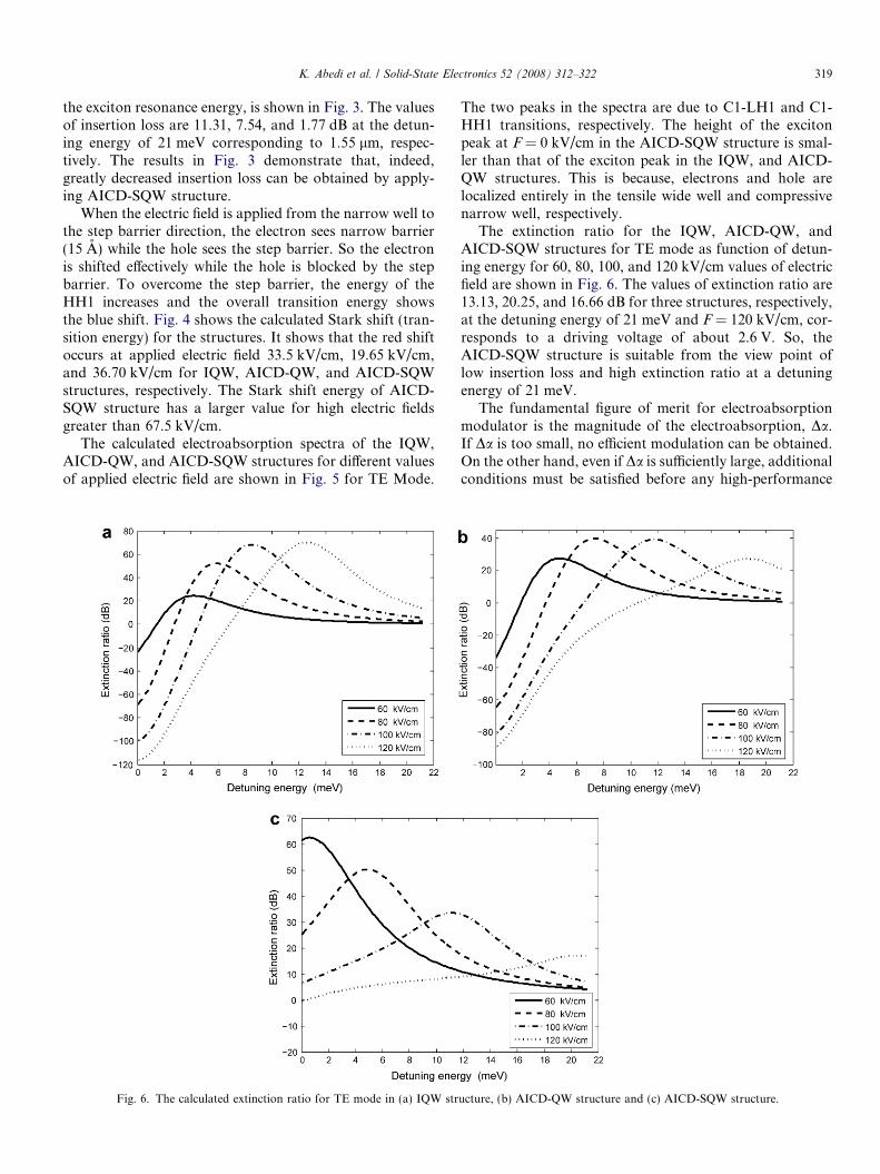
The extinction ratio for the IQW, AICD-QW, andAICD-SQW structures for TE mode as function of detun-ing energy for 60, 80, 100, and 120 kV/cm values of electricfield are shown in Fig. 6. The values of extinction ratio are13.13, 20.25, and 16.66 dB for three structures, respectively,at the detuning energy of 21 meV and F = 120 kV/cm, cor-responds to a driving voltage of about 2.6 V. So, theAICD-SQW structure is suitable from the view point oflow insertion loss and high extinction ratio at a detuningenergy of 21 meV.
The fundamental figure of merit for electroabsorptionmodulator is the magnitude of the electroabsorption, Da.If Da is too small, no efficient modulation can be obtained.On the other hand, even if Da is sufficiently large, additionalconditions must be satisfied before any high-performance
ucture, (b) AICD-QW structure and (c) AICD-SQW structure.
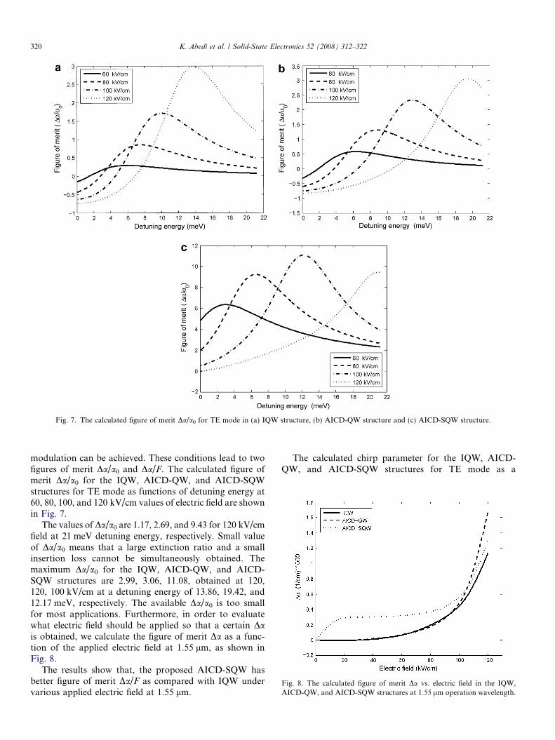
Fig. 7. The calculated figure of merit Da/a0 for TE mode in (a) IQW structure, (b) AICD-QW structure and (c) AICD-SQW structure.
Fig. 8. The calculated figure of merit Da vs. electric field in the IQW,AICD-QW, and AICD-SQW structures at 1.55 lm operation wavelength.
320 K. Abedi et al. / Solid-State Electronics 52 (2008) 312–322
modulation can be achieved. These conditions lead to twofigures of merit Da/a0 and Da/F. The calculated figure ofmerit Da/a0 for the IQW, AICD-QW, and AICD-SQWstructures for TE mode as functions of detuning energy at60, 80, 100, and 120 kV/cm values of electric field are shownin Fig. 7.
The values of Da/a0 are 1.17, 2.69, and 9.43 for 120 kV/cmfield at 21 meV detuning energy, respectively. Small valueof Da/a0 means that a large extinction ratio and a smallinsertion loss cannot be simultaneously obtained. Themaximum Da/a0 for the IQW, AICD-QW, and AICD-SQW structures are 2.99, 3.06, 11.08, obtained at 120,120, 100 kV/cm at a detuning energy of 13.86, 19.42, and12.17 meV, respectively. The available Da/a0 is too smallfor most applications. Furthermore, in order to evaluatewhat electric field should be applied so that a certain Dais obtained, we calculate the figure of merit Da as a func-tion of the applied electric field at 1.55 lm, as shown inFig. 8.
The results show that, the proposed AICD-SQW hasbetter figure of merit Da/F as compared with IQW undervarious applied electric field at 1.55 lm.
The calculated chirp parameter for the IQW, AICD-QW, and AICD-SQW structures for TE mode as a
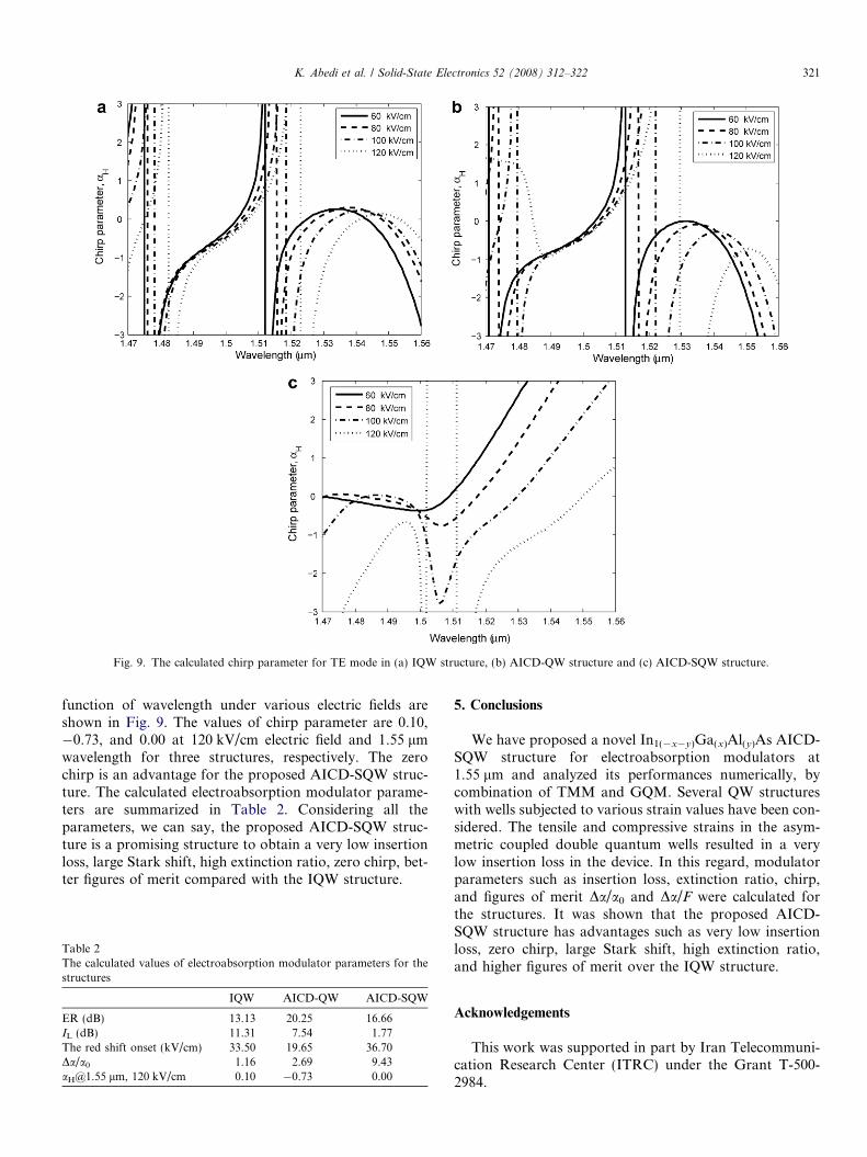
Fig. 9. The calculated chirp parameter for TE mode in (a) IQW structure, (b) AICD-QW structure and (c) AICD-SQW structure.
K. Abedi et al. / Solid-State Electronics 52 (2008) 312–322 321
function of wavelength under various electric fields areshown in Fig. 9. The values of chirp parameter are 0.10,�0.73, and 0.00 at 120 kV/cm electric field and 1.55 lmwavelength for three structures, respectively. The zerochirp is an advantage for the proposed AICD-SQW struc-ture. The calculated electroabsorption modulator parame-ters are summarized in Table 2. Considering all theparameters, we can say, the proposed AICD-SQW struc-ture is a promising structure to obtain a very low insertionloss, large Stark shift, high extinction ratio, zero chirp, bet-ter figures of merit compared with the IQW structure.
Table 2The calculated values of electroabsorption modulator parameters for thestructures
IQW AICD-QW AICD-SQW
ER (dB) 13.13 20.25 16.66IL (dB) 11.31 7.54 1.77The red shift onset (kV/cm) 33.50 19.65 36.70Da/a0 1.16 2.69 [email protected] lm, 120 kV/cm 0.10 �0.73 0.00
5. Conclusions
We have proposed a novel In1(�x�y)Ga(x)Al(y)As AICD-SQW structure for electroabsorption modulators at1.55 lm and analyzed its performances numerically, bycombination of TMM and GQM. Several QW structureswith wells subjected to various strain values have been con-sidered. The tensile and compressive strains in the asym-metric coupled double quantum wells resulted in a verylow insertion loss in the device. In this regard, modulatorparameters such as insertion loss, extinction ratio, chirp,and figures of merit Da/a0 and Da/F were calculated forthe structures. It was shown that the proposed AICD-SQW structure has advantages such as very low insertionloss, zero chirp, large Stark shift, high extinction ratio,and higher figures of merit over the IQW structure.
Acknowledgements
This work was supported in part by Iran Telecommuni-cation Research Center (ITRC) under the Grant T-500-2984.

322 K. Abedi et al. / Solid-State Electronics 52 (2008) 312–322
References
[1] Irmscher S, Lewen R, Eriksson U. InP–InGaAsP high-speed travel-ing-wave electroabsorption modulators with integrated terminationresistors. IEEE Photon Technol Lett 2002;14:923–5.
[2] Pappert SA, Orazi RJ, Vu TT, Lin SC, Clawson AR, Yu PKL.Polarization dependence of a 1.52 lm InGaAs/InP multiple quantumwell waveguide electroabsorption modulator. IEEE Photonics Tech-nol Lett 1990;2:257–9.
[3] Wood TH, Pastalan JZ, Burrus CA, Johnson BC, Miller BI,deMiguel JL, et al. Electric field screening by photogenerated holesin multiple quantum wells: a new mechanism for absorptionsaturation. Appl Phys Lett 1990;57:1081–3.
[4] Sahara R, Morito K, Sato K, Kotaki Y, Soda H, Okazaki N.Strongly improved frequency response at high-optical input powersfrom InGaAsP compensated strain MQW etectroabsorption modu-lators. IEEE Photonics Technol Lett 1995;7:1004–6.
[5] Loi KK, Sakamoto I, Mei XB, Tu CW, Chang WSC. High efficiency1.3 lm InAsP–GaInP MQW electroabsorption modulators formicrowave fiber-optic links. IEEE Photonics Technol Lett1996;8:626–8.
[6] Shin D-S, Yu PKL, Pappert SA. High-power electroabsorptionmodulator using intra-step- barrier quantum wells. J Appl Phys2001;89:1515–7.
[7] Shin D-S. Effect of a step barrier on the quantum-confined Starkeffect and applications to electroabsorption modulators with highsaturation optical power. J Korean Phys Soc 2005;41:364–70.
[8] Chuang SL. Efficient band-structure calculations of strained quantumwells. Phys Rev B 1991;43:9649–61.
[9] Darabi E, Ahmadi V, Mirabbaszadeh K. Numerical analysis of anoptoelectronic integrated device composed of coupled periodic MQWphototransistor and strained-QW laser diode. Solid State Electron2006;50:473–9.
[10] Chao CY, Chuang SL. Momentum-space solution of exciton excitedstates and heavy hole–light hole mixing in quantum wells. Phys Rev B1993;48:8210–21.
[11] Chin MK, Chang WSC. Electroabsorption properties of InGaAs/InAlAs multiple quantum well structures at 1.5 lm. IEEE PhotonTechnol Lett 1994;6:502–4.
[12] Minch J, Park SH, Keating T, Chuang SL. Theory and experiment ofIn(1�x) Ga(x)As(y)P(1�y) and In(1�x�y)Ga(x)Al(y)As long-wavelengthstrained quantum-well lasers. IEEE J Quantum Electron1999;35:771–82.
[13] Zhang Y, Chen W, Wang A, Jiang H, Liu C, Liu S. Design of theactive structure of high-performance 1.55 lm In1�x�yGayAlxAsstrained MQW lasers. IEEE J Quantum Electron 2001;37:771–2.
[14] Nakamura K, Shimizu A, Fujii K, Koshiba M, Hayata K. Numericalanalysis of the absorption and the refractive index change in arbitrarysemiconductor quantum well structures. IEEE J Quantum Electron1992;28:1670–7.
[15] Lafait J, Yamaguchi T, Frigerio JM, Bichri A, Driss-Khodja H.Effective medium equivalent to a symmetric multilayer at obliqueincidence. Appl Opt 1999;29:2460–5.
[16] Yamanaka C, Wakita K, Yokoyama K. Potential chirp-free charac-teristics (negative chirp parameter) in electroabsorption modulatorsusing a wide tensile-strained quantum well structure. Appl Phys Lett1996;69:3114–6.
Copyright © 2022 FDOKUMEN