Quantum transport in a cylindrical sub-0.1 μm silicon-based MOSFET
Upload
independentCategory
view
0download
0
High-sensitivity 10 Gbps Ge-on-Si photoreceiver operating at λ ~1.55 µm
Jiho Joo,1,2
Sanghoon Kim,1 In Gyoo Kim,
1 Ki-Seok Jang,
1
and Gyungock Kim1,2,*
1Electronics & Telecommunications Research Institute, Gajeong-dong, Yuseong-gu, Daejeon, 305-700, Korea
2University of Science and Technology, 52, Eoeun-dong, Yuseong-gu, Daejeon, 305-333, Korea *[email protected]
Abstract: We present a high-sensitivity photoreceiver based on a vertical- illumination-type 100% Ge-on-Si photodetector. The fabricated p-i-n photodetector with a 90 µm-diameter mesa shows the −3 dB bandwidth of 7.7 GHz, and the responsivity of 0.9 A/W at λ~1.55 µm, corresponding to the external quantum efficiency of 72%. A TO-can packaged Ge photoreceiver exhibits the sensitivity of −18.5 dBm for a BER of 10−12 at data rate of 10 Gbps. This result proves the capability of a cost-effective 100% Ge-on-Si photoreceiver which can readily replace the III-V counterparts for optical communications.
©2010 Optical Society of America
OCIS codes: (040.6040) silicon detectors; (130.0250) Optoelectronics; (040.5160) Photodetectors; (060.4510) Optical communications; (200.4650) Optical interconnects.
References and links
1. M. Haurylau, G. Chen, H. Chen, J. Zhang, N. A. Nelson, D. H. Albonesi, E. G. Friedman, and P. M. Fauchet, “On-Chip Optical Interconnect Roadmap: Challenges and Critical Directions,” IEEE J. Sel. Top. Quantum Electron. 12(6), 1699–1705 (2006).
2. K. Preston, L. Chen, S. Manipatruni, and M. Lipson, “Silicon Photonic Interconnect with Micrometer-Scale Devices” 6th International conference on Group IV photonics, WA2, pp.1–3 (2009).
3. A. Shacham, K. Bergman, and L. P. Carloni, “Photonic Networks-on- Chip for Future Generations of Chip Multiprocessors,” IEEE Trans. Comput. 57(9), 1246–1260 (2008).
4. L. Colace, and G. Assanto, “Germanium on Silicon for Near-Infrared Light Sensing,” IEEE Photon. J. 1(2), 69–79 (2009).
5. M. S. Rasras, D. M. Gill, M. P. Earnshaw, C. R. Doerr, J. S. Weiner, C. A. Bolle, and Y.-K. Chen, “CMOS Silicon Receiver Integrated With Ge Detector and Reconfigurable Optical Filter,” IEEE Photon. Technol. Lett. 22(2), 112–114 (2010).
6. J.-M. Hartmann, A. Abbadie, A. M. Papon, P. Holliger, G. Rolland, T. Billon, J.-M. Fédéli, M. Rouvière, L. Vivien, and S. Laval, “Reduced pressure–chemical vapor deposition of Ge thick layers on Si.001. for 1.3–1.55-µm photodetection,” J. Appl. Phys. 95(10), 5905–5913 (2004).
7. Y. Ishikawa, K. Wada, D. D. Cannon, J. Liu, H. Luan, and L. C. Kimerling, “Strain-induced band gap shrinkage in Ge grown on Si substrate,” Appl. Phys. Lett. 82(13), 2044–2046 (2003).
8. J. Liu, D. D. Cannon, K. Wada, Y. Ishikawa, S. Jongthammanurak, D. T. Danielson, J. Michel, and L. C. Kimerling, “Tensile strained Ge p-i-n photodetectors on Si platform for C and L band telecommunications,” Appl. Phys. Lett. 87(1), 011110 (2005).
9. X. Zheng, F. Liu, D. Patil, H. Thacker, Y. Luo, T. Pinguet, A. Mekis, J. Yao, G. Li, J. Shi, K. Raj, J. Lexau, E. Alon, R. Ho, J. E. Cunningham, and A. V. Krishnamoorthy, “A sub-picojoule-per-bit CMOS photonic receiver for densely integrated systems,” Opt. Express 18(1), 204–211 (2010).
10. Y. Kang, H.-D. Liu, M. Morse, M. J. Paniccia, M. Zadka, S. Litski, G. Sarid, A. Pauchard, Y.-H. Kuo, H.-W. Chen, W. S. Zaoui, J. E. Bowers, A. Beling, D. C. McIntosh, X. Zheng, and J. C. Campbell, “Monolithic germanium/silicon avalanche photodiodes with 340 GHz gain–bandwidth product,” Nat. Photonics 3(1), 59–63 (2009).
11. S. Assefa, F. Xia, and Y. A. Vlasov, “Reinventing germanium avalanche photodetector for nanophotonic on-chip optical interconnects,” Nature 464(7285), 80–84 (2010).
12. G. Dehlinger, S. J. Koester, J. D. Schaub, J. O. Chu, Q. C. Ouyang, and A. Grill, “High-speed Germanium-on-SOI lateral PIN photodiodes,” IEEE Photon. Technol. Lett. 16(11), 2547–2549 (2004).
13. L. Vivien, J. Osmond, J. M. Fédéli, D. Marris-Morini, P. Crozat, J. F. Damlencourt, E. Cassan, Y. Lecunff, and S. Laval, “42 GHz p.i.n Germanium photodetector integrated in a silicon-on-insulator waveguide,” Opt. Express 17(8), 6252–6257 (2009).
14. M. Morse, O. Dosunmu, T. Yin, Y. Kang, H. D. Liu, G. Sarid, E. Ginsburg, R. Cohen, S. Litski, and M. Zadka, “Performance of Ge/Si receivers at 1310 nm,” Physica E 41(6), 1076–1081 (2009).
#128716 - $15.00 USD Received 20 May 2010; revised 1 Jul 2010; accepted 15 Jul 2010; published 21 Jul 2010(C) 2010 OSA 2 August 2010 / Vol. 18, No. 16 / OPTICS EXPRESS 16474
15. H. Yu, S. Ren, W. S. Jung, A. K. Okyay, D. A. B. Miller, and K. C. Saraswat, “High-Efficiency p-i-n Photodetectors on Selective-Area-Grown Ge for Monolithic Integration,” IEEE Electron Device Lett. 30, 1161–1163 (2009).
16. D. Suh, S. Kim, J. Joo, and G. Kim, “36-GHz High-Responsivity Ge Photodetectors Grown by RPCVD,” IEEE Photon. Technol. Lett. 21(10), 672–674 (2009).
17. M. Jutzi, M. Berroth, G. Wöhl, M. Oehme, and E. Kasper, “Ge-on-Si Vertical Incidence Photodiodes with 39-GHz Bandwidth,” IEEE Photon. Technol. Lett. 17(7), 1510–1512 (2005).
18. Y. Ishikawa, J. Osaka and K. Wada, “Germanium Photodetectors in Silicon Photonics” IEEE Laser & Electro-Optics Society conf., pp.367–368 (2009).
19. T. H. Loh, H. S. Nguyen, R. Murthy, M. B. Yu, W. Y. Loh, G. Q. Lo, N. Balasubramanian, D. L. Kwong, J. Wang, and S. J. Lee, “Selective epitaxial germanium on silicon-on-insulator high speed photodetectors using low-temperature ultrathin Si0.8Ge0.2 buffer,” Appl. Phys. Lett. 91(7), 073503 (2007).
20. G. Kim, I. Kim, J. Baek, and O. Kwon, “Enhanced frequency response associated with negative photoconductance in an InGaAs/InAlAs avalanche photodetector,” Appl. Phys. Lett. 83(6), 1249–1251 (2003).
21. J.-W. Shi, Y.-S. Wu, Z.-R. Li, and P.-S. Chen, “Impact-ionization-induced bandwidth enhancement of a Si-SiGe-based avalanche photodiode operating at a wavelength of 830 nm with a gain-bandwidth product of 428 GHz,” IEEE Photon. Technol. Lett. 19(7), 474–476 (2007).
Progress of Silicon photonics technology can provide cost-effective optical communication devices by facilitating the mature silicon CMOS fabrication technology [1–5]. The 100% Ge-on-Si photodetector (PD) has been perceived as the best candidate for the Si-based photodetector operating at near-infrared (IR), since the germanium has large absorption coefficient at near-IR frequencies, and the compatibility of parallel processing with silicon [6–8]. Recently, the performance of the 100% Ge-on-Si photodetectors has shown remarkable progress. The reported waveguide-type Ge photodetectors have proven the high-speed and high-responsivity characteristics, comparable to the photodetector based on III-V compound semiconductors [9–14]. Also, there have been reports on the vertical-illumination type photodetectors which show progress and improvements in performance [15–19,21]. However, the simultaneous achievement of both high-speed and high-responsivity characteristics in the vertical-illumination type Ge photodetector for practical applications in optical telecommunications has not been reported yet.
In this paper, we report a vertical-illumination type 100% Ge-on-Si photodetector which shows high-responsivity characteristics sufficient for practical application for a 10 Gbps photoreceiver with a performance comparable to the commercial photoreceiver for optical communications.
Ge epitaxial layers were grown on phosphorous-implanted 6” Si (100) wafers by reduced pressure chemical vapor deposition (RPCVD). A 0.11 µm-thick Ge single-crystal seed layer grown at 400 °C was followed by a Ge absorption layer grown at 650 °C without further thermal annealing process. Figure 1(a) shows the measured ω-2θ scans around (004) diffraction order of a Ge epitaxial layer by high-resolution x-ray diffraction (HRXRD). In the figure, as the thickness of the Ge layer increases from 1.2 µm to 5 µm, the peak intensity of ωGe related to the Ge epilayer increases with decreasing FWHM, and the peak position shifts right toward the silicon peak indicating the increase of the residual strain. From
( )004
2
sinGe
Ge
aλ
ω
⊥= and Cu Kα1 wavelength λ = 1.5406 Å, the lattice parameter aGe
⊥ in the
normal direction to the growth plane decreases from 5.6514 Å to 5.6504 Å, as the thickness of Ge layer increases from 1.2 µm to 5 µm in the figure. From the strain relationship of the in-plane (aGe
) and the perpendicular (aGe⊥) lattice parameters of the epitaxially grown Ge layer
to the bulk [6], the calculated tensile-strain onto the Si (001) substrate increases 0.154% to 0.177% as the thickness of Ge layer increases for 1.2 µm to 5 µm. Figure 1(b) shows the atomic force microscope (AFM) and cross-sectional high-resolution transmission electron microscope (HRTEM) images of a 3 µm-thick Ge layer. The measured RMS surface roughness is ~0.541 nm. For a 5 µm-thick layer case, the RMS surface roughness decreases down to 0.298 nm. Around ± 1% thickness uniformity of the epilayer was achieved on a 6” silicon wafer. A 0.1 µm-thick p-type poly-silicon was deposited on the Ge epi-layer for the device fabrication. The doping levels of p- and n-contact layers were 5 × 10²⁰/cm3 and 1 × 10¹⁹/cm3, respectively. The devices were fabricated with the CMOS compatible process of I-
#128716 - $15.00 USD Received 20 May 2010; revised 1 Jul 2010; accepted 15 Jul 2010; published 21 Jul 2010(C) 2010 OSA 2 August 2010 / Vol. 18, No. 16 / OPTICS EXPRESS 16475

line photolithography, etching and metallization and alloying process with Ti/TiN/Al_1%Si/TiN. Mesas with diameters ranging from 40 µm to 160 µm were defined by reactive ion etch (RIE). A SiO2 layer was used for passivation and anti-reflection coating.
3 3 .0 3 3 .5 3 4 .0 3 4 .51 0
0
1 01
1 02
1 03
1 04
1 05
1 06
1 07
33.00 33.05 33.1010
0
101
102
103
104
105
106
G e = 1 .2 µm
G e = 1.7 µm
G e = 3 µm
G e = 4 µm
G e = 5 µm
G e
Inte
nsity (a.u
.)
ωωωω (((( o ))))
G eS i
Inte
nsit
y (
a.u
.)
ωωωω (((( o ))))
(a )
(b)
3 3 .0 3 3 .5 3 4 .0 3 4 .51 0
0
1 01
1 02
1 03
1 04
1 05
1 06
1 07
33.00 33.05 33.1010
0
101
102
103
104
105
106
G e = 1 .2 µm
G e = 1.7 µm
G e = 3 µm
G e = 4 µm
G e = 5 µm
G e
Inte
nsity (a.u
.)
ωωωω (((( o ))))
G eS i
Inte
nsit
y (
a.u
.)
ωωωω (((( o ))))
(a )
(b)
Fig. 1. (a) High resolution ω-2θ x-ray-diffraction profiles around the (004) order for the Ge epilayers grown on silicon wafers. (b) AFM and TEM mages of the 3 µm-thick Ge epilayer on silicon.
Figure 2(a) shows a schematic cross-section of a vertical-illumination type p-i-n Ge photodetector structure. Figure 2(b) shows a top-view SEM image of the fabricated 90-µm diameter device with a 4 µm-thick Ge absorption layer, and Fig. 2(c) is the 52 degree-tilted cross sectional SEM image of the device prepared by Focused Ion Beam (FIB) milling process.
Figure 3(a) shows the measured current-voltage (J-V) characteristics of a 90 µm-diameter device with a 4-µm thick Ge layer. The measured dark current is 666 nA at −1 V. The light was delivered to the device by a lensed optical fiber probe. The photocurrent is measured under the illumination of λ~1.55 µm and λ~1.31 µm. The current under illumination tends to decrease slightly as the applied reverse bias increases [20]. The measured responsivity (R) is
0.9 A/W and the external quantum efficiency, ( )int
1.24(1 ) 1 W
ext
R h Rr e
q
ανη η
λ
−⋅ ⋅= = = − − is
72%. The absorption coefficient, α, was estimated as 3460 cm−1, with a unity internal quantum efficiency and the measured surface reflection r~5% on the top of the device at λ~1.55 µm. Figure 3(b) shows measured responsivity spectra of 160 µm-diameter devices with 1.2 µm- to
#128716 - $15.00 USD Received 20 May 2010; revised 1 Jul 2010; accepted 15 Jul 2010; published 21 Jul 2010(C) 2010 OSA 2 August 2010 / Vol. 18, No. 16 / OPTICS EXPRESS 16476

Fig. 2. (a) Cross-sectional scheme of the fabricated Ge-on-Si PD, (b) top-view SEM image of the fabricated 90 µm-diameter device with 4 µm-thick Ge absorption layer, and (c) 52 degree-tilted cross sectional SEM image of the device prepared by FIB milling.
4 µm-thick Ge layers in the wavelength ranges of 1.25 µm –1.35 µm, and 1.52 µm – 1.66 µm. In the figure, as the Ge layer thickness (W) increases, overall enhancement of the
responsivity is observed. The responsivity (the quantum efficiency) of the device with a 4 µm-thick Ge layer is 1.0 A/W (82%) at λ~1.52 µm and 0.94 A/W (75%) at λ~1.55 µm. Also, the measured responsivity at λ~1.31 µm is 1.02 A/W, corresponding to the external quantum efficiency of 96.4%. Also the increase of the strain can be responsible for the responsivity improvement in the wavelength region beyond 1.55 µm up to L-band wavelength region, such as, R~0.75 A/W at λ~1.57 µm and R~0.2 A/W at λ~1.60 µm. Inset plots the spectral responsivity ratio normalized with respect to the resposivity at λ = 1.52 µm for each device in the wavelength
1.30 1.40 1.50 1.60
0.0
0.5
1.0
1.5
2.0
1.52 1.56 1.60 1 .6 40.0
0.2
0.4
0.6
0.8
1.0
1.2 µµµµm -thic k G e
3.0 µµµµm -thic k G e
4.0 µµµµm -thic k G e
No
rma
lize
d r
es
po
ns
ivit
y
W avelen gth (((( µµµµm ))))
1.2 µµµµm-thick Ge
3.0 µµµµm-thick Ge
4.0 µµµµm-thick Ge
Re
sp
on
siv
ity
(A
/W)
Wavelength (((( µµµµm ))))
(b)
-5 -4 -3 -2 -1 010
-7
10-6
10-5
10-4
10-3
10-2
Illuminated @ λλλλ ~ 1.55 µµµµm
Cu
rren
t (A
)
Voltage (V)
Dark current
(a)
1.30 1.40 1.50 1.60
0.0
0.5
1.0
1.5
2.0
1.52 1.56 1.60 1 .6 40.0
0.2
0.4
0.6
0.8
1.0
1.2 µµµµm -thick G e
3.0 µµµµm -thick G e
4.0 µµµµm -thick G e
No
rma
lize
d r
es
po
ns
ivit
y
W avelen gth (((( µµµµm ))))
1.2 µµµµm-thick Ge
3.0 µµµµm-thick Ge
4.0 µµµµm-thick Ge
Re
sp
on
siv
ity
(A
/W)
Wavelength (((( µµµµm ))))
(b)
-5 -4 -3 -2 -1 010
-7
10-6
10-5
10-4
10-3
10-2
Illuminated @ λλλλ ~ 1.55 µµµµm
Cu
rren
t (A
)
Voltage (V)
Dark current
(a)
Fig. 3. (a) The measured current-voltage characteristic of a 90 µm-diameter device with a 4 µm-thick Ge layer. The solid line indicates the dark current. The photocurrent is measured under illumination of λ~1.55 µm. (b) The measured responsivity spectra of 160 µm-diameter devices with 1.2 µm- to 4 µm-thick Ge layers in the wavelength ranges of 1.25 µm–1.35 µm, and 1.52 µm–1.66 µm. Inset shows the spectral responsivity-ratio normalized with respect to the value at λ = 1.52 µm for the wavelength range of 1.52 µm–1.66 µm.
range of 1.52 µm – 1.66 µm, which exhibits the relative upheaval of the responsivity in the wavelength region beyond 1.55 µm as the thickness of a Ge absorption layer increases from
#128716 - $15.00 USD Received 20 May 2010; revised 1 Jul 2010; accepted 15 Jul 2010; published 21 Jul 2010(C) 2010 OSA 2 August 2010 / Vol. 18, No. 16 / OPTICS EXPRESS 16477

1.2 µm to 4 µm. A dip structure in each responsivity curve near λ~1.3 µm is due to the effect of a fixed antireflection coating thickness optimized for λ~1.55 µm.
The frequency response of a Ge PD was measured by using a 20 GHz Agilent 8730A lightwave component analyzer. Figure 4(a) shows the normalized frequency response for various diameter devices with 4 µm-thick Ge absorption layer. The −3 dB bandwidth (f-3dB) of the device is 13.4 GHz to 2.6 GHz, as the diameter of the device increases from 40 to 160 µm at −3 V [20,21]. Figure 4(b) plots the dependency of f-3dB (left axis, black line) and responsivity (right axis, blue line) on the device diameter at λ~1.55 µm. As the mesa diameter increases, the responsivity shows slow increase, whereas the bandwidth decreases rapidly. As shown in the figure, 60 µm- to 90 µm-diameter devices are good candidates for the 10 Gbps application with sufficient responsivity. A device with larger diameter mesa can have advantage since it can ease up the optical packaging burden. The f-3dB of a 90 µm-diameter device is 7.7 GHz for a 4 µm-thick Ge absorption layer case and 8.2 GHz for a 3 µm-thick Ge absorption layer case. For 60um-diameter device case, as the Ge-layer thickness increases from 3 um to 4 um, the bandwidth decreases from 13.4 GHz to 9.8 GHz.
0 5 10 15 20-12
-9
-6
-3
0
3
6
(a)
60 µµµµm90 µµµµm
160 µµµµm
40 µµµµm
Vext
= 3 V
No
rmalized
resp
on
se (
dB
)
Frequency (GHz)40 60 80 100 120 140 160
0
5
10
15
20
0.0
0.2
0.4
0.6
0.8
1.0
@ λλλλ ~ 1550 nm
Vext
= -3 V
-3d
B b
an
dw
idth
(G
Hz)
Device diameter (um)
(b)
Resp
on
siv
ity (A
/W)
0 5 10 15 20-12
-9
-6
-3
0
3
6
(a)
60 µµµµm90 µµµµm
160 µµµµm
40 µµµµm
Vext
= 3 V
No
rmalize
d r
esp
on
se (
dB
)
Frequency (GHz)40 60 80 100 120 140 160
0
5
10
15
20
0.0
0.2
0.4
0.6
0.8
1.0
@ λλλλ ~ 1550 nm
Vext
= -3 V
-3d
B b
an
dw
idth
(G
Hz)
Device diameter (um)
(b)
Resp
on
siv
ity (A
/W)
Fig. 4. (a) The on-chip measurement of the frequency response for various diameter devices with a 4 µm-thick Ge absorption layer. The −3 dB bandwidth (f-3dB) of the device is 13.4 GHz to 3.5 GHz, as the diameter of the device increases from 40 to 160 µm at −3 V. (b) The dependency of the f-3dB (black line, left axis) and the responsivity (blue line, right axis) on the device diameter at λ ~1.55 µm.
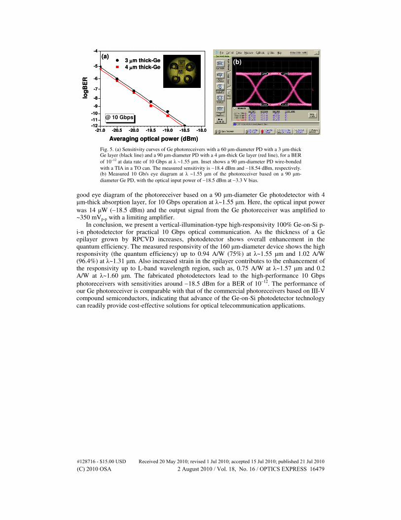
High responsivity of a photodetector is core element requisite to the high-sensitivity photoreceiver. Figure 5(a) displays the sensitivity curves of TO-can packaged Ge photoreceivers measured at λ~1.55 µm. A 60 µm-diameter device with a 3 µm-thick Ge layer (black line) or a 90 µm-diameter device with a 4 µm-thick Ge layer (red line) was wire-bonded with a transimpedance amplifier (TIA), which has 4 kΩ gain with f-3dB > 7 GHz and is commonly used for the packaging in III-V compound-semiconductor-based photoreceivers. The microscope image of a ROSA for a TO-can packaged photoreceiver is shown in inset of Fig. 5(a). Each receiver shows the sensitivity of −18.4 dBm and −18.54 dBm, respectively, for a BER of 10−12 at data rate of 10 Gbps with supply voltage of 3.3 V. These results are comparable with those of commercial III-V compound-semiconductor photoreceivers, and prove the capability of cost-effective Ge photodetectors which can readily replace the III-V counterparts for optical communications. Even better sensitivity of a Ge photoreceiver is expected for the shorter wavelength of λ~1.31 µm. An eye diagram with 231-1 non-return-to-zero (NRZ) pseudo-random bit sequence was measured using Agilent 86100C digital communication analyzer and Anristu MP1758A pulse pattern generator. Figure 5(b) exhibits a
#128716 - $15.00 USD Received 20 May 2010; revised 1 Jul 2010; accepted 15 Jul 2010; published 21 Jul 2010(C) 2010 OSA 2 August 2010 / Vol. 18, No. 16 / OPTICS EXPRESS 16478
-21.0 -20.5 -20.0 -19.5 -19.0 -18.5 -18.0-12
-11
-10
-9
-8
-7
-6
-5
-4
@ 10 Gbps
3 µµµµm thick-Ge
4 µµµµm thick-Ge
Averaging optical power (dBm)
log
BE
R
(a)(b)
-21.0 -20.5 -20.0 -19.5 -19.0 -18.5 -18.0-12
-11
-10
-9
-8
-7
-6
-5
-4
@ 10 Gbps
3 µµµµm thick-Ge
4 µµµµm thick-Ge
Averaging optical power (dBm)
log
BE
R
(a)(b)
Fig. 5. (a) Sensitivity curves of Ge photoreceivers with a 60 µm-diameter PD with a 3 µm-thick Ge layer (black line) and a 90 µm-diameter PD with a 4 µm-thick Ge layer (red line), for a BER of 10−12 at data rate of 10 Gbps at λ ~1.55 µm. Inset shows a 90 µm-diameter PD wire-bonded with a TIA in a TO can. The measured sensitivity is −18.4 dBm and −18.54 dBm, respectively. (b) Measured 10 Gb/s eye diagram at λ ~1.55 µm of the photoreceiver based on a 90 µm-diameter Ge PD, with the optical input power of −18.5 dBm at −3.3 V bias.
good eye diagram of the photoreceiver based on a 90 µm-diameter Ge photodetector with 4 µm-thick absorption layer, for 10 Gbps operation at λ~1.55 µm. Here, the optical input power was 14 µW (−18.5 dBm) and the output signal from the Ge photoreceiver was amplified to ~350 mVp-p with a limiting amplifier.
In conclusion, we present a vertical-illumination-type high-responsivity 100% Ge-on-Si p-i-n photodetector for practical 10 Gbps optical communication. As the thickness of a Ge epilayer grown by RPCVD increases, photodetector shows overall enhancement in the quantum efficiency. The measured responsivity of the 160 µm-diameter device shows the high responsivity (the quantum efficiency) up to 0.94 A/W (75%) at λ~1.55 µm and 1.02 A/W (96.4%) at λ~1.31 µm. Also increased strain in the epilayer contributes to the enhancement of the responsivity up to L-band wavelength region, such as, 0.75 A/W at λ~1.57 µm and 0.2 A/W at λ~1.60 µm. The fabricated photodetectors lead to the high-performance 10 Gbps photoreceivers with sensitivities around −18.5 dBm for a BER of 10−12. The performance of our Ge photoreceiver is comparable with that of the commercial photoreceivers based on III-V compound semiconductors, indicating that advance of the Ge-on-Si photodetector technology can readily provide cost-effective solutions for optical telecommunication applications.
#128716 - $15.00 USD Received 20 May 2010; revised 1 Jul 2010; accepted 15 Jul 2010; published 21 Jul 2010(C) 2010 OSA 2 August 2010 / Vol. 18, No. 16 / OPTICS EXPRESS 16479
Copyright © 2022 FDOKUMEN