The Role of the Carrier Mass in Semiconductor Quantum Dots
26
arXiv:cond-mat/9902310v1 23 Feb 1999 The Role of the Carrier Mass in Semiconductor Quantum Dots M. S. Chhabra, V. Ranjan, and Vijay A. Singh Physics Department, I.I.T.-Kanpur, U.P. 208106, INDIA (January 1999) Abstract In the present work we undertake a re-examination of effective mass theory (EMT) for a semiconductor quantum dot. We take into account the fact that the effective mass (m i ) of the carrier inside the dot of radius R is distinct from the mass (m o ) in the dielectric coating surrounding the dot. The electronic structure of the quantum dot is determined in crucial ways by the mass dis- continuity factor β ≡ m i /m o . In this connection we propose a novel quantum scale, σ, which is a dimensionless parameter proportional to β 2 V 0 R 2 , where V 0 represents the barrier due to dielectric coating. The scale σ represents a mass modified “strength ” of the potential. We show both by numerical calculations and asymptotic analysis that the charge density near the nanocrystallite sur- face, ρ(r = R), can be large and scales as 1/σ. This fact suggests a significant role for the surface in an EMT based model. We also show that the upshift in the ground state energy is weaker than quadratic, unlike traditional EMT based calculations, and chart its dependence on the proposed scale σ. Finally, we demonstrate that calculations based on our model compare favorably with valence band photoemission data and with more elaborate theoretical calcu- lations. PACS INDEX: 71.24.+q, 73.20.Dx, 78.66.-w, 61.46.+w Typeset using REVT E X 1
-
Upload
independent -
Category
Documents
-
view
2 -
download
0
Transcript of The Role of the Carrier Mass in Semiconductor Quantum Dots

arX
iv:c
ond-
mat
/990
2310
v1 2
3 Fe
b 19
99
The Role of the Carrier Mass in Semiconductor Quantum Dots
M. S. Chhabra, V. Ranjan, and Vijay A. Singh
Physics Department, I.I.T.-Kanpur, U.P. 208106, INDIA
(January 1999)
Abstract
In the present work we undertake a re-examination of effective mass theory
(EMT) for a semiconductor quantum dot. We take into account the fact that
the effective mass (mi) of the carrier inside the dot of radius R is distinct from
the mass (mo) in the dielectric coating surrounding the dot. The electronic
structure of the quantum dot is determined in crucial ways by the mass dis-
continuity factor β ≡ mi/mo. In this connection we propose a novel quantum
scale, σ, which is a dimensionless parameter proportional to β2V0R2, where V0
represents the barrier due to dielectric coating. The scale σ represents a mass
modified “strength” of the potential. We show both by numerical calculations
and asymptotic analysis that the charge density near the nanocrystallite sur-
face, ρ(r = R), can be large and scales as 1/σ. This fact suggests a significant
role for the surface in an EMT based model. We also show that the upshift
in the ground state energy is weaker than quadratic, unlike traditional EMT
based calculations, and chart its dependence on the proposed scale σ. Finally,
we demonstrate that calculations based on our model compare favorably with
valence band photoemission data and with more elaborate theoretical calcu-
lations.
PACS INDEX: 71.24.+q, 73.20.Dx, 78.66.-w, 61.46.+w
Typeset using REVTEX
1
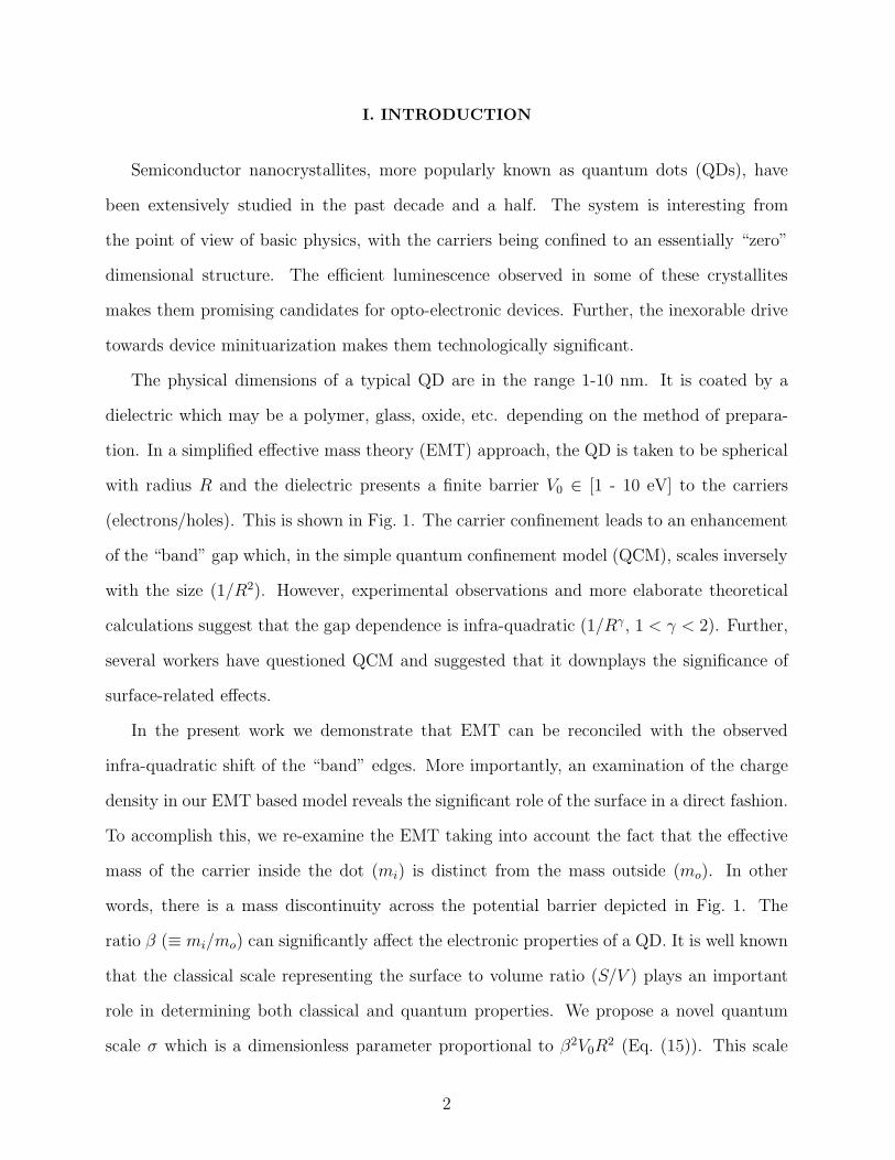
I. INTRODUCTION
Semiconductor nanocrystallites, more popularly known as quantum dots (QDs), have
been extensively studied in the past decade and a half. The system is interesting from
the point of view of basic physics, with the carriers being confined to an essentially “zero”
dimensional structure. The efficient luminescence observed in some of these crystallites
makes them promising candidates for opto-electronic devices. Further, the inexorable drive
towards device minituarization makes them technologically significant.
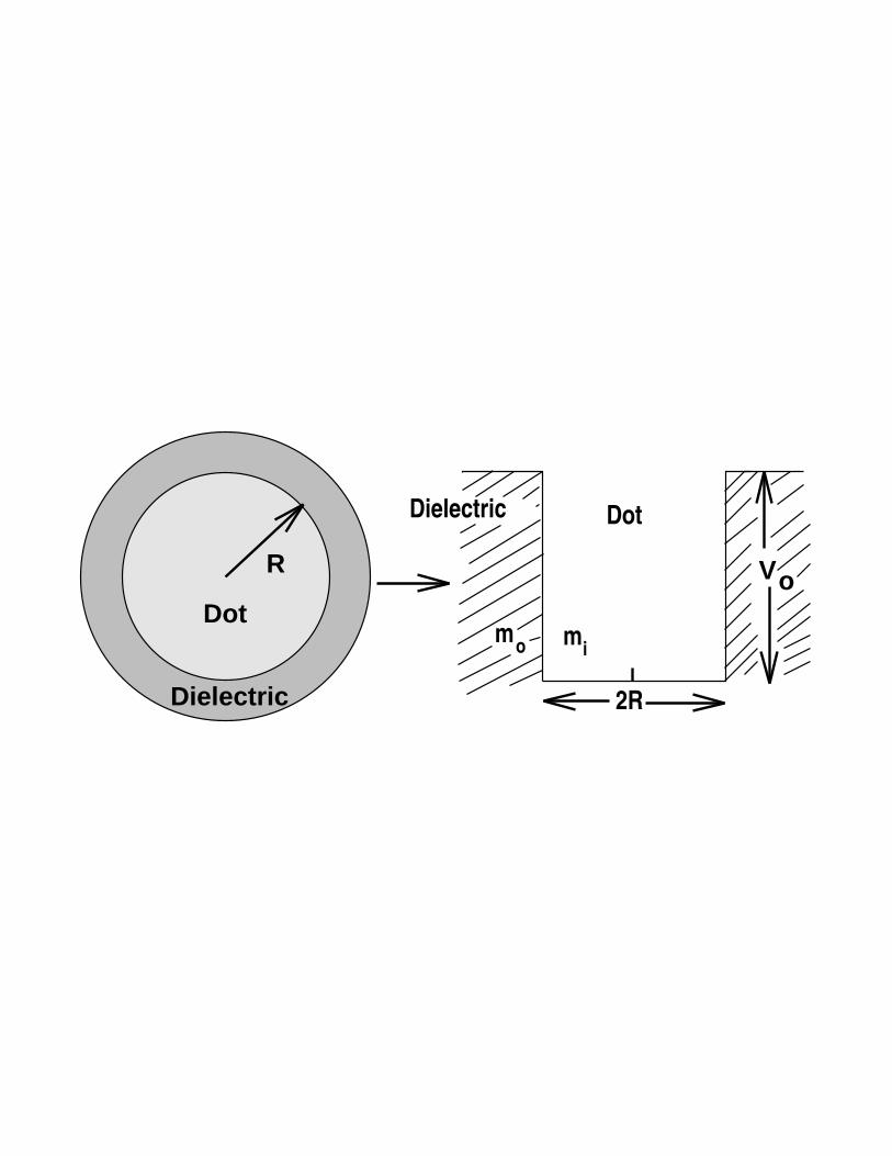
The physical dimensions of a typical QD are in the range 1-10 nm. It is coated by a
dielectric which may be a polymer, glass, oxide, etc. depending on the method of prepara-
tion. In a simplified effective mass theory (EMT) approach, the QD is taken to be spherical
with radius R and the dielectric presents a finite barrier V0 ∈ [1 - 10 eV] to the carriers
(electrons/holes). This is shown in Fig. 1. The carrier confinement leads to an enhancement
of the “band” gap which, in the simple quantum confinement model (QCM), scales inversely
with the size (1/R2). However, experimental observations and more elaborate theoretical
calculations suggest that the gap dependence is infra-quadratic (1/Rγ, 1 < γ < 2). Further,
several workers have questioned QCM and suggested that it downplays the significance of
surface-related effects.
In the present work we demonstrate that EMT can be reconciled with the observed
infra-quadratic shift of the “band” edges. More importantly, an examination of the charge
density in our EMT based model reveals the significant role of the surface in a direct fashion.
To accomplish this, we re-examine the EMT taking into account the fact that the effective
mass of the carrier inside the dot (mi) is distinct from the mass outside (mo). In other
words, there is a mass discontinuity across the potential barrier depicted in Fig. 1. The
ratio β (≡ mi/mo) can significantly affect the electronic properties of a QD. It is well known
that the classical scale representing the surface to volume ratio (S/V ) plays an important
role in determining both classical and quantum properties. We propose a novel quantum
scale σ which is a dimensionless parameter proportional to β2V0R2 (Eq. (15)). This scale
2

represents a mass modified “strength” of the potential (MSP). The correction to the ground
state energy E1 and the charge density at the interface ρ(r = R) scale in an appealingly
simple way with the proposed scale σ.
In Sec. II we describe the basic model in brief. The carrier (electron/hole) is confined to
a spherical QD of radius R with a finite barrier of height V0 (see Fig. 1). As suggested by
Brus1, the BenDaniel-Duke boundary conditions2 are appropriate for a system with a mass
discontinuity across the barrier. This aspect has been ignored in a number of theoretical
calculations in the past (see Sec. V). As will be shown subsequently, the physics of the
problem is determined in crucial ways by the mass discontinuity factor β(≡ mi/mo). A
pedagogical point, we highlight is that the BenDaniel-Duke boundary conditions must be
applied to the full wavefunction and not to the partial wavefunction. The error involved in
employing the partial wavefunction can be substantial and is presented in Table I.
The numerical results are presented in Sec. III. Previous works in the field have devoted
considerable attention to the upshift of the ground state energy E1. We focus instead on the
charge density ρ(r). Brus1 had pointed out that the charge density near the nanocrystallite
surface can be large if the carrier effective mass mi is small. We show that the charge density
at the nanocrystallite boundary ρ(r = R) is indeed large if β (= mi/mo) is small (Fig. 3).
A more complete picture is provided by our proposed MSP scale σ (∝ β2V0R2). In Fig. 4
we demonstrate that ρ(R) scales inversely with σ. For a quantum dot, S/V ratio is large.
Thus the fraction of unsaturated bonds on the surface increases and/or the formation of
molecular complexes on the surface is favoured. The large charge density on the surface
suggests a novel non-classical reason for the importance of the surface. We also show that
the ground state energy E1 exhibits a size dependence which is weaker than the quadratic
(1/R2) dependence one has come to expect from EMT (Fig. 5).
A detailed asymptotic analysis is presented in Sec. IV to explain the numerical results of
Sec. III and to present them in terms of the proposed quantum scale σ. We show that ρ(R)
scales as ≃ 1/σ. We introduce the notion of the peneteration depth δ in this connection.
We also explain the infra-quadratic dependence of the ground state energy on the size R. In
3

particular, we demonstrate that the correction to the quadratic term scales as ∼ −1/√σ.
Section V constitutes the discussion. We show that our model compares favourably
with the experimental valence-band photoemission data of Colvin et. al.3 on CdS (Fig. 6)
and with more elaborate tight-binding calculations4 (Fig. 7). We summarize our work and
suggest directions for future research.
II. BASIC THEORY
We consider a spherical semiconductor nanocrystallite of diameter d = 2R (See Fig. 1).
An additional electron in the “conduction band” of such a crystallite is described in effective
mass theory by the Hamiltonian:
H = − h2
2~∇ ·
(
1
m∗(~r)· ~∇
)
+ V (~r) (1)
For a position dependent mass the appropriate hermitian kinetic energy operator is given
by the first term on the right hand side of Eq. (1)2. The electron effective mass inside the
nanocrystallite (mi) is different from the effective mass in the dielectric coating (mo). A
useful parameter is the ratio (β) of the effective masses.
β =mi
mo
(2)
For the experimentally relevant cases explored in the last two decades, β is less than unity.
For extreme cases, such as GaAs or InAs quantum dots, β equals 0.067 and 0.02, respectively,
where we have taken mo = me, the free electron mass. An important aspect of the present
study is to highlight the significance of this parameter β. The potential V(r) in Eq. (1) is
given by
V (r) =
0 r ≤ 0
Vo r > R(3)
Here Vo is a large positive potential and represents the dielectric coating surrounding the
nanocrystallite (See Fig. 1). Typically a nanocrystallite is surrounded by dielectrics such
4

as glasses, polymers, organic solvents or oxides and hydrides5. Thus, the electron is in a
spherically symmetric well. The wavefunction for this spherically symmetric problem can
be written in the form:
ψnlm(r) = Rnl(r)Ylm(θ, φ) (4)
where the symbols have their usual meanings. It is customary to write the radial wavefunc-
tion Rnl as:
unl(r) = rRnl (5)
The equation for the partial wavefunction unl(r) is :
d2unl
dr2− l(l + 1)
r2unl +
2miE
h2unl = 0 (6)
where mi is the mass of the electron inside the potential well. The electron effective mass
m∗ assumes different values mi inside and mo outside the well.
For the l = 0 case, the standard form for the radial wavefunction is obtained on solving
Eq. (6). This is :
Rn0(r) = Asin(kin
n r)
kinn r
(7)
for 0 < r < R and
Rn0(r) = Be−kout
nr
koutn r
(8)
for r > R, where
kinn =
√
2miEn
h2(9)
and,
koutn =
√
2mo(Vo − En)
h2(10)
and A and B are normalization constants.
5

Standard text books on quantum mechanics state the condition of continuity of the
derivative of the wavefunction inside and outside the well as :
dRnl
dr
∣
∣
∣
∣
∣
r→R−
=dRnl
dr
∣
∣
∣
∣
∣
r→R+
(11)
However, as has been discussed in the semiconductor literature, this condition must be
replaced by the BenDaniel-Duke condition in case the effective masses are different across
the interface. The condition now reads
1
mi
dRnl
dr
∣
∣
∣
∣
∣
r→R−
=1
mo
dRnl
dr
∣
∣
∣
∣
∣
r→R+
(12)
A further point needs to be made at this stage. Many textbooks, in the process of the
solution of the Schrodinger equation, define the partial wavefunction unl (Eq. (5)) and then
further state that the continuity conditions at the interface may be imposed on unl(r)6–8.
They claim that this would yield the same eigenvalue conditions as imposing these conditions
on Rnl(r) would. Quoting Schiff6, “ The energy levels are obtained by ...(this is equivalent
to making 1/R dR/dr continuous there)”. It is shown that this is manifestly incorrect when
we use the modified boundary condition. It is further shown that in the limit the effective
masses become equal across the interface, the two treatments indeed become equivalent for
this special case. Imposition of the modified boundary condition on the full wave function
leads, after some algebraic manipulations, to
kinn cot(kin
n R) = −βkoutn +
1 − β
R(13)
whereas, the use of the same condition on the partial wavefunction unl(r) leads to
kinn cot(kin
n R) = −βkoutn (14)
The two conditions are evidently quite different. However, they agree when β is unity, recov-
ering thereby the elementary case. There are three parameters, β, V0 and R, in the above
transcendental equation. As can be readily seen from the two equations, the eigenvalues
calculated using Eq. (13) would deviate more and more from those calculated using Eq. (14)
6

for smaller β and smaller R. The energy eigenvalues obtained for a particular set of param-
eters is presented in Table I. For β=0.1, V0=1.0 and R=20.0 Ao, the disagreement is even
worse, being as large as 57%. In the sections that follow, we shall employ Eq. (13).
III. RESULTS
In this section, we present the results of our numerical calculations. Further, this section
and the next contains the interpretation of our results. In what follows, we focus our
attention on the spherically symmetric (l = 0) case.
A quantity of central interest to us is the radial charge density ρ(r)
ρ(r) = r2R2
n0(r)
Where the multiplicative constant, e, the carrier charge, has been ignored. We examine
the dependence of the equilibrium charge density on the ratio of the effective masses β
(≡ mi/mo), the barrier height V0 and the radius of the nanocrystallite R. In Fig. 2, we
have plotted the charge density for different values of β and V0 = 1.5 eV. The radius of the
crystallite is R = 50 Ao. As can be readily seen, the value of the equilibrium charge density
at the crystallite boundary, ρ(r = R), falls rapidly with increasing β. The peak in the charge
density occurs at r ∈ [R/2, R]; in other words, close to the surface of the crystallite. For
small values of β, the peak is at r ≃ R. Examples of small β are InP, InAs, GaAs, etc. Even
if the carrier is photogenerated in the interior of the crystallite, it rapidly redistributes itself
such that the equilibrium charge density is large near the boundary. In nanocrystallites with
large β(≃ 1) the peak in the charge density shifts towards R/2. In other words r = R/2 is
a “fixed point” for the charge density. Figure 3 shows this more systematically. We have
plotted the charge density at the boundary as a function of β, and taking V0 = 5 eV. There
is a clear decrease in the charge density as the value of β increases. In the next section,
we shall show this more rigorously in the limit of large V0. An appropriate perspective on
ρ(r = R) is obtained by defining a mass modified “strength” of the potential (MSP), σ.
7

σ = (βκ0R)2 (15)
κ0 =
√
2moV0
h2
Conventional textbooks6,9 define the strength of potential as V0R2. As will become apparent
in the next section, a more appropriate definition for the case under study is σ = (βκ0R)2.
Figure 4 depicts that ρ(r) falls with σ. This decrease is observed to be nearly linear. We
shall have occasion to examine this universal parameter parameter σ in the next section.
In Fig. 5 we study the dependence of the ground state energy E1 (n = 1, l = 0) of the
carrier on the crystallite size R. We have taken V0 = 5 eV for this figure. We observe that
this dependence is infraquadratic, i.e. weaker than 1/R2. We note that this infraquadratic
behaviour has been reported both experimentally and on the basis of tight-binding (TB)
calculations10,11. In the present case infraquadratic behaviour can be traced to the finite
nature of the barrier and the change of the effective mass across the barrier. Inspection of
Fig. 5 reveals that with decreasing value of β, the behaviour increasingly departs from the
quadratic case. This is demonstrated rigorously in the next section on asymptotic analysis
(Eq. (23)), where we see that
E1 =c1R2
− c2R3
(16)
c1 and c2 being constants. An attempt to coerce the above expression into the form
E1 ≃C
Rγ(17)
will yield 1 < γ < 2. We have presented the salient results of our model in this sec-
tion. Additional results related to experiments and earlier theoretical calculation on specific
semiconductor nanocrystallites will be presented in the last section (Sec. V). The following
section on asymptotic analysis will attempt to explain the numerical results obtained in this
section.
8

IV. ASYMPTOTIC ANALYSIS
We now present an asymptotic analysis of Eq. (13) in an attempt to explain the results
of our calculations in the previous section. For an infinite potential well, the eigenvalue
condition reduces to :
kinn R = nπ (18)
where kinn is defined in Eq. (9). We consider the case of the ground state i.e. n = 1. For a
well which is “sufficiently” deep but finite, we approximate the above expression by :
kin1R = π − ǫ (19)
where ǫ is a small number. Using Eq. (19) in Eq. (13), we obtain :
ǫ
π≃ 1
β(1 + κoR)(20)
where κo =
√
2moVo
h2(21)
where we have assumed that Vo ≫ E1, the ground state energy. The condition on the
smallness of ǫ is now apparent. If either of these parameters β, R, Vo is large then ǫ would
be small. It is clear that ǫ is inversely dependent on the mass modified “strength” of the
potential defined earlier in Eq. (15)
ǫ ≃ π√σ
(22)
when√σ ≫ β. We are now in a position to obtain an approximate expression for the
ground state energy E1. Using Eqs. (19) and (20) and the definition of kin1
from Eq. (9),
one obtains,
E1 =π2h2
2miR2
[
1 − 2
βκoR+ . . .
]
(23)
=π2h2
2miR2
[
1 − 2√σ
+ . . .
]
(24)
9
Thus one can see that the ground state energy has the size dependence depicted in Fig. 5,
namely,
E1 =C1
R2− C2
R3(25)
≃ C
Rγ(26)
with effective exponent γ < 2, as mentioned earlier. The EMT literature on nanocrystallite
semiconductors commonly quote γ = 2. However, absorption and luminescence experiments
as well as the tight-binding calculations10,11 yield γ < 2 . We have thus formally demon-
strated how even within the EMT approach, an infraquadratic exponent (γ < 2) is obtained.
The calculation depicted in Fig. 5 attests to this.
Garrett12 has proposed a penetration depth for the one dimensional finite well problem
with β = 1. We define an analogous penetration depth (δ) for the carrier in the three
dimensional potential well and for the general case β 6= 1.
δ =1
βκo
=R√σ
(27)
Next we shall examine the charge density at the surface. An appealing, intuitive way to
understand the nature of ρ(r = R) is to use the concept of the penetration depth. It is
easy to see from Eq. (27) that the penetration depth will be large in case β is small. This is
already a confirmation of the result that the charge density is large at the boundary for small
β (Figs. 2 and 3). Thus one would expect that when the carrier mass in the semiconductor
is small (InSb, GaAs, CdS) then the charge density at the interface will be large. The
penetration depth δ indicates the extent of the wavefunction penetration into the forbidden
region.
We can present a more rigorous analysis of ρ(r = R) by examining the wavefunction.
The normalized wavefunction inside the potential well is :
R10(r) = Asin(kin
1r)
kin1 r
(28)
10

where A =kin
1√4π
[
R
2
(
1 − sin(2kin1R)
2kin1 R
)
+1 − cos(2kin
1R)
4kout1
]
−1
2
(29)
Using Eq. (19) in Eq. (28), we obtain after some algebraic manipulations:
R10(r) ≈ A(
1 +ǫ
π
)
[
sin(πr/R)
πr/R− ǫ
πcos
(
πr
R
)
]
(30)
whence we get for the charge density ρ,
ρ(ǫ, r) ≡ r2R2
10(r) = A2
(
1 +ǫ
π
)2[
(
R
π
)2
sin2
(
πr
R
)
+(
rǫ
π
)2
cos2
(
πr
R
)
−(
ǫrR
π2
)
sin(
2πr
R
)
]
(31)
The charge density at the interface is:
ρ(R) = r2R2
10(r)∣
∣
∣
r=R= A2
(
1 +ǫ
π
)(
ǫ
π
)2
R2 (32)
Recall that ǫ2 ∼ 1/σ (≡ 1/(βκoR)2). It is therefore clear that ρ(r = R) would fall with
increasing β. This prediction is in agreement with Fig. 3 where ρ(R) is 1/β1.85.
Within the range of validity of approximation in Eq. (19), ǫ is much less than unity.
Therefore, Eq. (32) may be written as
ρ(R) ≈ A2R2
σ(33)
One can thus understand the inverse dependence of ρ(R) on σ in Fig. 4. It is interesting to
note that the charge density can be related to the penetration depth defined in Eq. (27),
ρ(R) ≈ A2δ2
One may also obtain the peak position, rpeak, in the charge density by a simple differentiation
of rR10(r), where R10(r) is given by Eq. (30). This yields
(
πrpeak
R
)
tan(
πrpeak
R
)
= −1 − ǫ/π
ǫ/π(34)
It can be seen easily, either by plotting Eq. (31) or by solving Eq. (34) numerically, that the
peak in the charge density ρ is located at values of R/2 ≤ r ≤ R and shifts to r = R/2 as
11

the value of ǫ is decreased. Decrease in ǫ is brought about by an increase in σ. Equation (34)
indicates that rpeak ∈ [R/2, R]. When β is small, rpeak > R/2 and this is also graphically
borne out by Fig. 2. Since the peak is shifted towards the crystallite boundary, the charge
density at the boundary becomes substantial. When the MSP scale σ is large, Eq. (34)
implies that rpeak → R/2. In other words there is a fixed-point or “attractor” at r = R/2.
The peak in the wavefunction does not shift to a value below R/2, no matter how large σ
is.
V. DISCUSSION
The objective of the present work is to explore EMT in the context of the variation of
the carrier effective mass across semiconductor - dielectric interface in a QD. We consider a
simple Hamiltonian described by Eq. (1) in order to illustrate the essential physics. It would
be worthwhile to compare our results with other theoretical calculations and experiments.
Below we present two such comparisons.
We compare our results with the valence band photoemission experiment carried out
by Colvin et. al. on CdS quantum dots3. Their work represents the first non-optical
observation of the electronic structure of semiconductor nanostructures. The experiment
measures the energy shift of the valence band maximum as the cluster size decreases, taking
the largest cluster of R = 35 Ao as a reference. For this case4, β = 0.53 and Fig. 6 depicts
the dependence of the valence band shift on the cluster size as calculated by us. We fit
our data to C/Rα. We get an exponent α = 1.26, which is in good agreement with the
experimental observation. Colvin et. al. attribute this shift to two factors : (i) the kinetic
energy enhancement due to the quantum confinement of the hole ; (ii) the polarization of
the crystallite and the loss of dielectric solvation energy1,13. As is clear from Fig. 6 a finite
barrier quantum confinement model with appropriate effective masses provides a reasonable
explanation for the experimental behaviour. We also note in passing that Takagahara has
argued that the polarization term can in general be neglected14.
12

Lippens and Lannoo4 have theoretically studied the same system. Our model can be
compared with their results for the valence band shift. Fig. 7 depicts such a comparison.
We have taken the barrier height V0 = 2 eV. A majority of the literature claim that TB
calculations are in better agreement with experiments. The EMT with quadratic dependence
on size (∼ 1/R2) represents an extreme case. As can be seen from Fig. 7 our EMT based
model is in close agreement with the experimental observations. On the other hand, the
standard EMT calculation of Lippens and Lannoo is at variance with their TB calculation.
The majority of the theoretical work for the absorption and luminescence in quantum
dots takes excitonic effects into account. In other words, the Hamiltonian involves both a
hole and an electron. We propose to extend our simple EMT model to the excitonic case as
well as to study excited states in the future. We also plan to study the capacitance of QDs
by analyzing multi-electron effects in our model.
We emphasize that the EMT calculation should be carried out with the correct boundary
condition as presented in Eq. (12). This fact has been pointed out by Brus1. The use of this
boundary condition leads to an eigenvalue condition (Eq. (13)) which is different from the
one normally encountered in textbooks6–8 (Eq. (14) with β = 1). A further point to note is
that the boundary condition must be imposed on full wavefunction Rnl(r). Imposing it on
the partial wavefunction unl(r) would lead to incorrect results.
EMT based calculations have normally been carried out using an infinite barrier15. In this
case, the charge density at the nanocrystallite boundary is zero. It is therefore not surprising
that the significance of the surface is downplayed. Further, workers who recognize the finite
nature of the barrier have ignored the mass discontinuity across the barrier16–19 and the
reason sometimes stated is that most of the population density of the carrier is still confined
well within QD16. The LDA based calculations on dot capacitance and shell filling effects also
ignore the mass discontinuity20. Porous silicon, which is a disordered agglomeration of silicon
nanocrystallites, presents a case-study for the debate between the quantum confinement
and the surface state schools of thought. This debate has been reviewed by a number of
workers21–24. In this work we have shown that the charge density can be large at the surface
13

even in an EMT based framework. This is more so for semiconducting materials with small
carrier effective masses and dielectric coatings representing a small potential barrier. Hence,
the contention that surface related effects are significant appears valid.
Another demerit of the infinite barrier model is its prediction of an inverse quadratic
(1/R2) shift of the band gap. We have already stated that this does not agree with exper-
iments and with more elaborate theoretical calculations10,11,25,26. We have shown through
our work that a calculation for finite barrier model leads to a good agreement with the
experimental infraquadratic dependence.
The highlights of the work are :
1. Ground state energy within EMT scales infraquadratically with the crystallite size
(Eq. (23) – (26)).
2. The parameter of relevance is our proposed mass modified “strength” of the potential,
the MSP scale σ = (βκoR)2. Our proposed parameter σ presents a more complete
picture of the physical situation than β alone does1.
3. The charge density at the boundary ρ(R) can be large (Figs (2) – (4)) and scales in-
versely with σ. This is unlike what one normally expects from EMT. In the literature
of semiconductor nanocrystallites there has been a longstanding debate between the-
ories for quantum confinement versus surface states21–24. The present work provides
a fresh perspective on the importance of surface related phenomena.
Acknowledgement
This work was supported by the Department of Atomic Energy through the Board of Re-
search in Nuclear Sciences, India (No. 37/11/97-R.&D.II). Discussions with Dr. Swapan
Ghosh of BARC are gratefully acknowledged.
14

REFERENCES
1 L. E. Brus, J. Chem. Phys. 79, 5566 (1983).
2 D. J. BenDaniel and C. B. Duke, Phys. Rev. 152, 683 (1966).
3 V. L. Colvin, A. P. Alivastos, and J. G. Tobin, Phys. Rev. Lett. 66, 2786 (1991).
4 P. E. Lippens and M. Lannoo, Phys. Rev. B 39, 10935 (1989).
5 Y. Wang and N. Herron, J. Chem. Phys. 95, 525 (1991).
6 L. Schiff, Quantum Mechanics, pp. 82-84 (McGraw-Hill Book Co., Singapore, 1968).
7 J. Powell and B. Crasemann, Quantum Mechanics (Addison-Wesley Publishing Co. Inc.,
New York, 1971).
8 F. Schwabl, Quantum Mechanics, pp 307 (Springer-Verlag, Berlin, 1992).
9 P. M. Mathews and K. Venkatesan, A Textbook of Quantum Mechanics, pp. 54 (Tata
McGraw-Hill Publishing Company Limited, New Delhi, 1990)
10 C. Delerue, G. Allan, and M. Lannoo, Phys. Rev. B 48, 11024 (1993).
11 V. Ranjan and V. A. Singh, in Proc. of the Ninth International Workshop on the Physics
of Semiconductor Devices, Delhi, INDIA (Narosa, London, 1998), pp. 98 – 101.
12 S. Garrett, Amer. J. Phys. 47, 195 (1979).
13 L. E. Brus, J. Chem. Phys. 80, 4403 (1984).
14 T. Takagahara, Phys. Rev. B 47, 4569 (1993).
15 U. Woggon, Optical Properties of Semiconductor Quantum Dots (Springer Verlag, Berlin,
1997), Vol. 136.
16 Y. Kayanuma and H. Momiji, Phys. Rev. B 41, 10261 (1990).
17 S. Nomura and T. Kobayashi, Sol. State Commun. 78, 677 (1991).
15

18 T. Shimura and M. Matsuura, Phys. Rev. B 56, 2109 (1997).
19 U. Laheld and G. Einevoll, Phys. Rev. B 55, 5184 (1997).
20 M. Macucci, K. Hess, and G. J. Iafarate, Phys. Rev. B 55, R4879 (1997).
21 Y. Kanemitsu, Phys. Reports 263, 1 (1995).
22 S. M. Prokes, J. Mater. Res. 11, 305 (1996).
23 A. G. Cullis, L. T. Canham, and P. D. J. Calcott, J. Appl. Phys. 82, 909 (1997).
24 G. C. John and V. A. Singh, Comments Cond. Matt. Phys. 18, 163 (1997).
25 H. Fu and A. Zunger, Phys. Rev. B 56, 1496 (1997).
26 S. Ogut, J. Chelikowsky, and S. Louie, Phys. Rev. Lett. 79, 1770 (1997).
16

TABLES
TABLE I. Comparison of eigenvalues obtained by applying the correct boundary condition on
the full wavefunction (Eq. (13)) and on the partial wavefunction (Eq. (14)). The values of the
parameters employed are β = 0.1, V0 = 2.5 eV and R = 40 Ao.
Eigenvalues with Eigenvalues with
full wavefunction partial wavefunction Percentage difference
0.13 0.15 12.04
0.61 0.65 3.21
1.52 1.56 2.53
17

FIGURES
FIG. 1. The left side of the figure depicts an idealized spherical quantum dot (QD) surrounded
by a dielectric coating. This is modeled by a potential well of height V0. The carrier effective mass
is mi inside the well and mo in the dielectric coating outside.
FIG. 2. A typical normalized charge density ρ(r) inside a crystallite of size R = 50 A. Note
that for small β = (mi/mo), ρ(r) is large at the crystallite surface (r = R). As β increases, the
position of the peak rpeak in ρ shifts to R/2.
FIG. 3. The charge density at the crystallite boundary, ρ(r = R). The charge density ρ(R) falls
with increasing β. We fit our data for ρ(R) to C1/βα, with α = 1.85. This is in good agreement
with the prediction of Eq. (32). C1 is a constant.
FIG. 4. The dependence of the charge density ρ(R) at the crystallite boundary on the proposed
quantum scale σ (≡ (βκ0R)2). The scale σ represents a mass modified “strength” of the potential
(see text). The data for ρ(R) fit well to C2/σα with α = 0.98, and in agreement with the prediction
of Eq. (33). C2 is a constant. The dotted line is a fit to the calculated data (diamonds).
FIG. 5. The ground state energy E1 versus the crystallite size R. The calculated data are for
four different values of β and are fitted to C/Rγ , where C is a constant. The values of γ for the
different values of β = 2.0, 0.4, 0.1 and 0.01 are respectively 1.95, 1.76, 1.39 and 1.03. We can see
that the energy shift is increasingly infraquadratic for smaller values of β.
FIG. 6. The data taken from the valence band photoemission spectra for CdS crystallite due
to Colvin et. al. (Ref. 3) is indicated by diamond symbols. Our calculation is indicated by the
dotted line. A fit to C/Rα leads to α = 1.26 for both cases. Our calculation gives a much improved
result as compared to traditional EMT with α = 2. See Sec. V for further discussion.
18

FIG. 7. Valence band shift with size of the CdS crystallite. Our results (solid line) are very close
to the tight-binding (TB) calculations (diamonds) of Lippens and Lannoo (Ref. 4). In contrast,
there is less agreement between the EMT (dashed line) and TB (diamond symbols) calculations of
Ref. 4.
19
VoR
2RDielectric
mi
Dotm
o
Dielectric Dot

r (Ao )
ρ ( r
) (a
rb. u
nit
s)
0
0.05
0.1
0.15
0.2
0.25
0 5 10 15 20 25 30 35 40 45 50
β = 0.05
β = 0.1
β = 0.5
β = 1.0β = 10.0

arb
. un
its)
((R
)ρ
0
500
1000
1500
2000
2500
3000
3500
4000
0.05 0.1 0.15 0.2 0.25 0.3β

σ (arb. units)
(R)
ρ(a
rb. u
nit
s)
0
500
1000
1500
2000
2500
3000
3500
0 200 400 600 800 1000 1200

E1
(eV
)
β = 0.01β = 0.1β = 0.4β = 2.0
0
0.2
0.4
0.6
0.8
1
1.2
1.4
10 20 30 40 50 60 70 80
R (Angstroms)

EV
B(e
V)
0.1
0.2
0.3
0.4
0.5
0.6
0.7
0.8
0.9
1
1.1
10 15 20 25 30 35 40
Our model
R (Angstroms)
Colvin et. al. [Ref. 3]

EV
B(e
V)
0
0.5
1
1.5
2
2.5
3
5 10 15 20 25 30 35 40 45 50 55
Ref. 4. (EMT)Ref. 4. (TB)
Our Model
R (Angstroms)