The role of the annealing temperature on the optical and structural properties of Eu doped GaN/AlN...
6
This article appeared in a journal published by Elsevier. The attached copy is furnished to the author for internal non-commercial research and education use, including for instruction at the authors institution and sharing with colleagues. Other uses, including reproduction and distribution, or selling or licensing copies, or posting to personal, institutional or third party websites are prohibited. In most cases authors are permitted to post their version of the article (e.g. in Word or Tex form) to their personal website or institutional repository. Authors requiring further information regarding Elsevier’s archiving and manuscript policies are encouraged to visit: http://www.elsevier.com/copyright
-
Upload
independent -
Category
Documents
-
view
0 -
download
0
Transcript of The role of the annealing temperature on the optical and structural properties of Eu doped GaN/AlN...
This article appeared in a journal published by Elsevier. The attachedcopy is furnished to the author for internal non-commercial researchand education use, including for instruction at the authors institution
and sharing with colleagues.
Other uses, including reproduction and distribution, or selling orlicensing copies, or posting to personal, institutional or third party
websites are prohibited.
In most cases authors are permitted to post their version of thearticle (e.g. in Word or Tex form) to their personal website orinstitutional repository. Authors requiring further information
regarding Elsevier’s archiving and manuscript policies areencouraged to visit:
http://www.elsevier.com/copyright
Author's personal copy
The role of the annealing temperature on the optical and structural propertiesof Eu doped GaN/AlN QD
M. Peres a, S. Magalhães a,b, J. Rodrigues a, M.J. Soares a, V. Fellmann d, A.J. Neves a, E. Alves b,c,B. Daudin d, K. Lorenz b,c, T. Monteiro a,⇑a Departamento de Física and i3N, Universidade de Aveiro, Aveiro 3810-193, Portugalb Instituto Tecnológico Nuclear, Sacavém 2686-953, Portugalc CFNUL, Av. Prof. Gama Pinto, 1649-003 Lisboa, Portugald CEA-CNRS, Institut Nanosciences et Cryogénie, 17 rue des Martyrs, Grenoble 38054, France
a r t i c l e i n f o
Article history:Received 8 July 2010Received in revised form 3 October 2010Accepted 20 October 2010Available online 18 November 2010
Keywords:GaNQuantum dotsRBSEu3+ luminescence
a b s t r a c t
Self assembled molecular beam epitaxy grown GaN quantum dots stacked with AlN spacers wereimplanted with Eu ions. The as-implanted samples were further submitted to thermal annealing treat-ments in nitrogen, between 1000 �C and 1200 �C. Eu3+ luminescence was observed in all samples withthe most intense emission assigned to the 5D0 ?
7F2 transition in the red spectral region. The preferentialexcitation paths of Eu3+ luminescence is explored using photoluminescence excitation measurementswhich allow us to identify the feeding mechanisms for the Eu3+ ions inside the GaN quantum dots andAlN host. Optically active Eu centres in both GaN QD and AlN layers could be identified. For low implan-tation fluence the Eu centres inside GaN QD are dominant while for high fluences the emission arisesfrom Eu in the AlN layers. The annealing temperature, on the other hand, does not cause any changein the local environment of the Eu-ions.
� 2010 Elsevier B.V. All rights reserved.
1. Introduction
Self assembled GaN quantum dots (QD) embedded in AlNspacer layers constitutes one of the multilayer systems particularlyattractive for optoelectronic device applications [1–5]. The GaN QDphotoluminescence (PL) energy is known to be dependent on thebalance between the carrier’s quantum confinement, strain stateand giant piezoelectric effects which are responsible for the obser-vation of GaN QD excitonic recombination above and below thebandgap of bulk GaN [6–11].
Rare earth elements have been widely used by the scientificcommunity to optically activate nitride based materials [12–17].Among them, Eu3+ luminescence due to transitions between the5D and 7F multiplets have been reported in the binary and ternaryAlxGa1�xN (0 6 x 6 1) hosts as well as in GaN QD/AlN superlatticeswhen doped either by ion implantation or by in situ growth [18–23]. Typically, the most intense intraionic luminescence in thewurtzite nitride structures is due to the 5D0 ?
7F2 transition whichoccurs in the red spectral region. In the Al1�xGaxN system it shiftsfrom ca. 622 to 624 nm when changing the composition from GaNto AlN. With their wide bandgap the nitride hosts are very suitable
to produce highly efficient Eu3+ related electroluminescent devicesas recently reported for MOVPE grown GaN:Eu [24]. In Eu-dopedGaN and AlN layers the nonradiative carrier recombination chan-nels severely limit the intra-4f6 luminescence efficiency, which isexpected to be surpassed with the incorporation of Eu3+ in GaNQD due to the strong confinement of the carriers in the dots andthe expected decrease of the nonradiative decay paths [25]. InGaN epilayers implanted with Eu the luminescence intensity wasfound to increase strongly with annealing temperature [26].
The purpose of the present article is to analyse the effects of theincreasing post-implant annealing temperature on the optical andstructural properties of Eu-doped GaN QD/AlN SL. Photolumines-cence (PL) and PL excitation (PLE) of the SL annealed at tempera-tures above 1000 �C is carried out to evaluate the role of theannealing temperature on excitation mechanisms of the Eu3+ emis-sion in the SL structures implanted with different fluences(1 � 1013 and 1 � 1015 ions cm�2).
2. Experimental
Two sets of GaN QD/AlN SL samples (#987 and #989) weregrown by molecular beam epitaxy (MBE) as described elsewhere[4].
The 20 periods SL structures were implanted at room tempera-ture (RT) with 300 keV Eu ions with fluences of 1 � 1013 and
0925-3467/$ - see front matter � 2010 Elsevier B.V. All rights reserved.doi:10.1016/j.optmat.2010.10.025
⇑ Corresponding author. Tel.: +351 234 370 824; fax: +351 234 378 197.E-mail address: [email protected] (T. Monteiro).
Optical Materials 33 (2011) 1045–1049
Contents lists available at ScienceDirect
Optical Materials
journal homepage: www.elsevier .com/locate /optmat
Author's personal copy
1 � 1015 ions cm�2. Post-implant annealing was performedbetween 1000 �C and 1200 �C in flowing N2 at 1 bar pressure andplacing a piece of AlN/sapphire face to face with the samples as aproximity cap. While sample 987 (high fluence) was cut into sev-eral pieces and annealed at different temperatures an isochronousannealing was performed for sample 989 (low fluence). The sam-ples characteristics are described in Table 1. Besides the SL struc-tures an additional �500 nm thick AlN layer implanted with1 � 1015 ions cm�2 and annealed at 1000 �C under the same condi-tions was used for comparison.
High resolution X-ray diffraction (HR-XRD) was performedusing CuKa1 radiation on a D8Discover system from Bruker-AXSusing a Göbel mirror, an asymmetric 2-bounce Ge(220) monochro-mator, and a 0.1 mm width slit placed in front of a scintillationdetector.
Steady state PL measurements were carried out between 14 Kand RT using the 325 nm line of a cw He–Cd laser or a 1000 WXe lamp coupled to a monochromator as excitation sources. Theused excitation energies are below the AlN bandgap. For the PLEmeasurements the emission monochromator was set in the Eu3+
emission lines and in the GaN QD excitonic recombination andthe excitation wavelength was scanned up to 240 nm. The spectrawere corrected to the lamp and optics.
3. Results and discussion
3.1. Low temperature PL
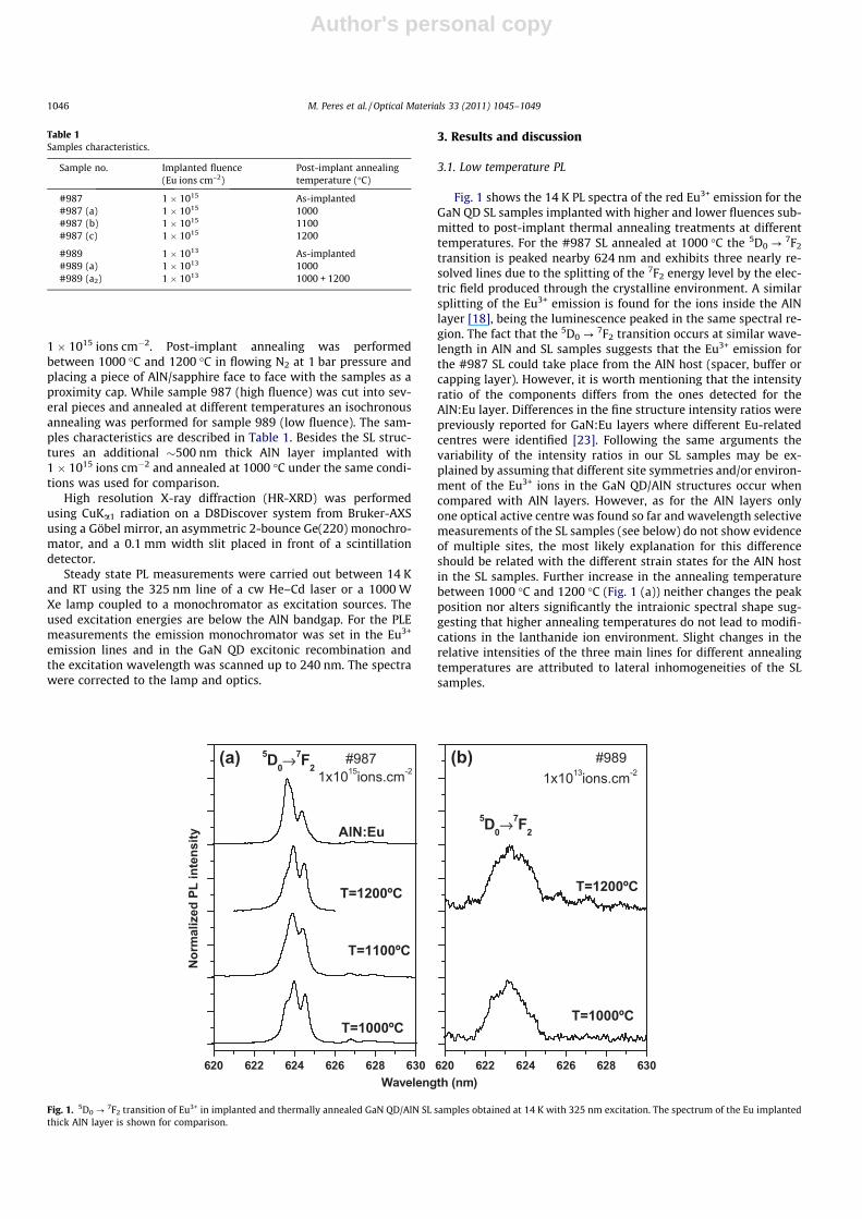
Fig. 1 shows the 14 K PL spectra of the red Eu3+ emission for theGaN QD SL samples implanted with higher and lower fluences sub-mitted to post-implant thermal annealing treatments at differenttemperatures. For the #987 SL annealed at 1000 �C the 5D0 ?
7F2
transition is peaked nearby 624 nm and exhibits three nearly re-solved lines due to the splitting of the 7F2 energy level by the elec-tric field produced through the crystalline environment. A similarsplitting of the Eu3+ emission is found for the ions inside the AlNlayer [18], being the luminescence peaked in the same spectral re-gion. The fact that the 5D0 ?
7F2 transition occurs at similar wave-length in AlN and SL samples suggests that the Eu3+ emission forthe #987 SL could take place from the AlN host (spacer, buffer orcapping layer). However, it is worth mentioning that the intensityratio of the components differs from the ones detected for theAlN:Eu layer. Differences in the fine structure intensity ratios werepreviously reported for GaN:Eu layers where different Eu-relatedcentres were identified [23]. Following the same arguments thevariability of the intensity ratios in our SL samples may be ex-plained by assuming that different site symmetries and/or environ-ment of the Eu3+ ions in the GaN QD/AlN structures occur whencompared with AlN layers. However, as for the AlN layers onlyone optical active centre was found so far and wavelength selectivemeasurements of the SL samples (see below) do not show evidenceof multiple sites, the most likely explanation for this differenceshould be related with the different strain states for the AlN hostin the SL samples. Further increase in the annealing temperaturebetween 1000 �C and 1200 �C (Fig. 1 (a)) neither changes the peakposition nor alters significantly the intraionic spectral shape sug-gesting that higher annealing temperatures do not lead to modifi-cations in the lanthanide ion environment. Slight changes in therelative intensities of the three main lines for different annealingtemperatures are attributed to lateral inhomogeneities of the SLsamples.
Table 1Samples characteristics.
Sample no. Implanted fluence(Eu ions cm–2)
Post-implant annealingtemperature (�C)
#987 1 � 1015 As-implanted#987 (a) 1 � 1015 1000#987 (b) 1 � 1015 1100#987 (c) 1 � 1015 1200
#989 1 � 1013 As-implanted#989 (a) 1 � 1013 1000#989 (a2) 1 � 1013 1000 + 1200
1x10¹⁵ions.cm-2
5D0→7F2
T=1200ºC
T=1100ºC
T=1000ºC
Nor
mal
ized
PL
inte
nsity
Wavelength (nm)
#987(a)
AlN:Eu
620 622 624 626 628 630 620 622 624 626 628 630
1x10¹³ions.cm-2
5D0→7F2
T=1200ºC
T=1000ºC
(b) #989
Fig. 1. 5D0 ?7F2 transition of Eu3+ in implanted and thermally annealed GaN QD/AlN SL samples obtained at 14 K with 325 nm excitation. The spectrum of the Eu implanted
thick AlN layer is shown for comparison.
1046 M. Peres et al. / Optical Materials 33 (2011) 1045–1049

Author's personal copy
A totally distinct 5D0 ?7F2 emission is measured for sample
#989. Though with low intensity the Eu3+ luminescence is nowslightly shifted to shorter wavelengths as expected for the observa-tion of the transition in the GaN host. The transition is peaked at623.2 nm close to the wavelength value found for the Eu3+ emis-sion in in situ doped GaN QD [19]. The small discrepancy couldbe due to different distribution of strain in the SL. The measuredPL suggests that for the low fluence implanted samples the Eu3+
emission arose mainly from the ions inside the GaN QD. Also, thethermal stability of the intraionic emission against the annealingtemperature is seen to be constant. As for the high fluence samplesno changes in the spectral shape are found for different annealingtemperatures.
3.2. Low temperature PLE
Fig. 2 shows the low temperature PLE spectra monitored at theEu3+ 5D0 ?
7F2 transition for the studied samples. Independently ofthe annealing temperature, for the SL implanted with higher flu-ence (Fig. 2(a)) two excitation bands with maxima at �265 nmand �345 nm are identified. For comparison purposes the PLE ofan AlN:Eu layer is also shown. Similar excitation bands were previ-ously reported in Eu-implanted AlN layers [20]. More recently,Wang et al. [18], assign the �265 nm and �345 nm excitationbands (labelled as X2 and X1 respectively) to the creation of core-excitonic complexes of Eu emitting centres. The observation ofthe X2 and X1 excitation bands for the high-fluence implantedGaN QD/AlN SL structures supports the conclusion that the Eu3+
luminescence arises from the AlN host. Moreover, the absence ofspectral modifications means that no changes in the Eu3+ excita-tion paths are promoted with increasing annealing temperaturesand strongly suggests that no changes on the ion environment inthe AlN host occurs.
For the SL implanted with lower fluence (Fig. 2(b)) the mainexcitation of the Eu3+ emission occurs via an asymmetric bandstarting nearby 350 nm and peaked �265 nm. The band has a pro-nounced shoulder at �300 nm and the X1 excitation band at
345 nm band is observed though with low intensity. The shoulderat �300 nm is completely absent in the high-fluence implanted SLwhen the PLE is monitored at Eu3+ emission.
In order to understand better the different physical mechanismswhich could be involved in the excitation of the Eu3+ ions in bothlow and high-fluence implanted and annealed samples we mustconsider potential excitation mechanisms from the individual lay-ers that constitute the SL. In this case a comparison with the PLEspectra of the GaN QD excitonic recombination as well as the PLE
AlN
1x10¹⁵ions.cm-2
T=1000ºC
T=1200ºC
T=1200ºC
T=1000ºC
T=1100ºC
PLE
inte
nsity
(arb
. uni
ts)
Wavelength (nm)
#987(a)
AlN:Eu
250 300 350 400 250 300 350 400
AlN
1x10¹³ions.cm-2
(b) #989
Fig. 2. Full lines: 14 K PLE spectra monitored at the 5D0 ?7F2 transition of Eu3+ ions for the thermally annealed GaN QD/AlN SL structures and Eu doped AlN layer.
Lines + symbols: 14 K PLE spectra monitored at the band maximum of GaN QD excitonic recombination. Dashed lines: PLE spectra monitored at 400 nm defect-related bandin an as-grown AlN layer.
620 622 624 626 628 630
T=1100ºC
Wavelength (nm)
Nor
mal
ized
PL
inte
nsity
1x10¹³ions.cm-2
5D0→7F2
T=1200ºC
T=1000ºC
#989
1x10¹⁵ions.cm-2#987
Fig. 3. Full lines: 5D0 ?7F2 transition of Eu3+ in implanted and thermally annealed
GaN QD/AlN SL samples obtained at 14 K with 325 nm excitation. Open symbols:spectra obtained with 350 nm excitation. Full symbols: spectra obtained with265 nm excitation.
M. Peres et al. / Optical Materials 33 (2011) 1045–1049 1047
Author's personal copy
from optically active centres in the undoped AlN layer must be ta-ken into account. In that sense two additional PLE spectra areshown in Fig 2(a): one monitored at the band maxima of theGaN QD excitonic recombination (at �465 nm) in sample #987and the other one monitored at �400 nm in the AlN layer whichcorresponds to the PL maximum of a defect related emission bandin the undoped AlN layer. The origin of this frequently observeddefect band is of disputed origin possibly related to a donor–accep-tor pair transitions involving Al vacancies [27]. As shown inFig. 2(a) the GaN QD excitonic recombination is mainly excitedvia two bands at �265 nm and �300 nm. The low energy excita-tion band is likely to be due to the GaN QD excited states [28].For the case of the high energy excitation band we must considerthat the excitation of QD is achieved via the defect band seen in un-doped AlN giving rise to the excitation band at ca. 250 nm whenmonitored at the maximum of this defect emission peak. Compar-ing the PLE spectra with the ones performed on the Eu3+ lumines-cence suggests that in the SL we must account for the overlappingof several excitation bands such as those related with the X1 and X2
bands in AlN [18,20], the defects in AlN and the excited states ofthe GaN QD. From the PLE data we can assume that for the SL im-planted with higher fluence (#987) the Eu3+ emission is mainly fedby the X1 and X2 excitation bands although we cannot exclude thatthe intraionic emission could in part be excited via the �250 nmband from the AlN-related defect levels. For the SL implanted withlower fluence (#989) and besides the X2 excitation band and the�250 nm band from AlN-related defect levels, the Eu3+ emissionis excited via the absorption through the excited states of theGaN QD, the asymmetric band near 300 nm.
3.3. Selective excited PL
Further information on the Eu3+ ion host location in the post-implant thermally annealed GaN QD/AlN SL can be obtained fromwavelength dependent PL measurements. Low temperature PLmeasurements were performed by exciting the two sets of SL sam-ples at 265 nm (via X2 and AlN-defect related excitation bands) and350 nm (via the X1 excitation band). The corresponding spectra areshown in Fig. 3 overlapped with the ones acquired with 325 nmexcitation. For samples implanted with high fluence no spectralchanges are detected on the 5D0 ?
7F2 transition when the Eu3+
emission is fed by the X2 and X1 excitation bands. However, forsamples implanted with lower fluence a spectral shift for the5D0 ?
7F2 transition is identified. With 265 nm and 325 nm excita-tion (matching the excited levels absorption of the GaN QD and AlNdefect band) the Eu-related centre is populated in the same way asthe GaN QD excitonic recombination. On the other hand, when theSL are excited at 350 nm, (the X1 band in AlN) the 5D0 ?
7F2 tran-sition is shifted to lower energies, nearby the 624 nm typical for
Eu3+ recombination in the AlN host. The data indicate that for the#989 SL Eu3+ luminescence from both hosts (GaN QD and AlN lay-ers) can be recognized.
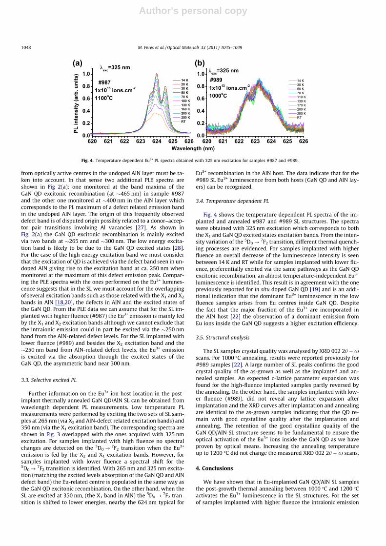
3.4. Temperature dependent PL
Fig. 4 shows the temperature dependent PL spectra of the im-planted and annealed #987 and #989 SL structures. The spectrawere obtained with 325 nm excitation which corresponds to boththe X1 and GaN QD excited states excitation bands. From the inten-sity variation of the 5D0 ?
7F2 transition, different thermal quench-ing processes are evidenced. For samples implanted with higherfluence an overall decrease of the luminescence intensity is seenbetween 14 K and RT while for samples implanted with lower flu-ence, preferentially excited via the same pathways as the GaN QDexcitonic recombination, an almost temperature-independent Eu3+
luminescence is identified. This result is in agreement with the onepreviously reported for in situ doped GaN QD [19] and is an addi-tional indication that the dominant Eu3+ luminescence in the lowfluence samples arises from Eu centres inside GaN QD. Despitethe fact that the major fraction of the Eu3+ are incorporated inthe AlN host [22] the observation of a dominant emission fromEu ions inside the GaN QD suggests a higher excitation efficiency.
3.5. Structural analysis
The SL samples crystal quality was analysed by XRD 002 2h �xscans. For 1000 �C annealing, results were reported previously for#989 samples [22]. A large number of SL peaks confirms the goodcrystal quality of the as-grown as well as the implanted and an-nealed samples. An expected c-lattice parameter expansion wasfound for the high-fluence implanted samples partly reversed bythe annealing. On the other hand, the samples implanted with low-er fluence (#989), did not reveal any lattice expansion afterimplantation and the XRD curves after implantation and annealingare identical to the as-grown samples indicating that the QD re-main with good crystalline quality after the implantation andannealing. The retention of the good crystalline quality of theGaN QD/AlN SL structure seems to be fundamental to ensure theoptical activation of the Eu3+ ions inside the GaN QD as we haveproven by optical means. Increasing the annealing temperatureup to 1200 �C did not change the measured XRD 002 2h �x scans.
4. Conclusions
We have shown that in Eu-implanted GaN QD/AlN SL samplesthe post-growth thermal annealing between 1000 �C and 1200 �Cactivates the Eu3+ luminescence in the SL structures. For the setof samples implanted with higher fluence the intraionic emission
620 621 622 623 624 625 6260.0
0.2
0.4
0.6
0.8
1.0
Wavelength (nm)
#987 PL
inte
nsity
(arb
. uni
ts)
14 K 20 K 30 K 50 K 70 K 100 K 130 K 160 K 200 K 250 K RT
λexc=325 nm
620 621 622 623 624 625 6260.0
0.2
0.4
0.6
0.8
1.0 14 K 30 K 50 K 70 K 110 K 130 K 170 K 200 K 280 K RT
1x10¹⁵ ions.cm-2
1100oC
#9891x1013 ions.cm-2
1000oC
λexc=325 nm(a) (b)
Fig. 4. Temperature dependent Eu3+ PL spectra obtained with 325 nm excitation for samples #987 and #989.
1048 M. Peres et al. / Optical Materials 33 (2011) 1045–1049
Author's personal copy
was seen to arise from AlN layers (buffer, spacer or capping). In thiscase the Eu3+ emission is mediated via the X2 and X1 excitationbands at 265 nm and 350 nm. Furthermore, temperature depen-dent PL studies show that the intraionic luminescence intensitydrops between 14 K and RT due to competing nonradiative pro-cesses. For the high-fluence implanted samples XRD measure-ments show an expansion of the average SL c-lattice parameterafter implantation. Thermal annealing at 1000 �C removes partiallythe lattice radiation damage which seems to be crucial to activatethe Eu3+ luminescence of the Eu ions inside the SL, however, higherannealing temperatures do not lead to further structural recoveryof the crystal.
In the SL samples implanted with lower fluence and submittedto post-implant thermal annealing, XRD 002 2h �x curves remainunchanged by implantation and annealing suggesting that the QDremain of good quality. The emission of the Eu3+ ions is character-ized by a broadening of the 5D0 ?
7F2 transition lines and the peakposition is shifted to shorter wavelengths compared to the highfluence samples. In this case the excitation paths of the Eu3+ emis-sion are equal to those populating the excitonic recombination ofthe quantum dots suggesting that the dominant optically activeEu centre is located inside the GaN QD. In addition a second Eu-re-lated centre can be identified arising from Eu3+ inside the AlN hostand preferentially excited at 350 nm. The Eu3+ emission is veryweak when compared with the GaN QD excitonic recombinationand practically no changes in the intraionic emission intensitywas seen with increasing annealing temperature suggesting thata maximum of the Eu3+ ions activation was already reached for1000 �C. In this context it is interesting to note that a rough esti-mate of the areal densities of QD and Eu indicates that in averagethe number of Eu ions incorporated inside QD is only �0.1–0.2 ionsper QD. The total number of Eu ions incorporated in AlN layers isabout 10 times higher than that inside QD. A persistent Eu3+ lumi-nescence was seen between 14 K and RT which is the expectedbehaviour for a luminescence that is fed by carriers that arestrongly confined in the dots. Increasing the annealing tempera-ture does not change the ion crystalline environments in both setsof samples.
Acknowledgements
We acknowledge the support by FCT, Portugal (PTDC/CTM/100756/2008). M. Peres and S. Magalhães thank FCT for their Grants,SFRH/BD/45774/2008 and SFRH/BD/44635/2008, respectively.
References
[1] T. Steiner (Ed.), Semiconductor Nanostructures for OptoelectronicApplications, Artech House Inc., 2004.
[2] H. Morkoç (Ed.), Handbook of Nitride Semiconductors and Devices, Wiley-VCH,2008.
[3] B. Daudin, F. Widmann, G. Feuillet, Y. Samson, M. Arlery, J.L. Rouvière, Phys.Rev. B 56 (1997) R7069.
[4] N. Gogneau, D. Jalabert, E. Monroy, T. Shibata, M. Tanaka, B. Daudin, J. Appl.Phys. 94 (2003) 2255.
[5] J. Brault, T. Huault, F. Natali, B. Damilano, D. Lefebvre, M. Leroux, M. Korytov, J.Massies, J. Appl. Phys. 105 (2009) 033519.
[6] G. Sarusi, O. Moshe, S. Khatsevich, D.H. Rich, B. Damilano, Phys. Rev. B 75(2007) 075306.
[7] F. Widmann, J. Simon, B. Daudin, G. Feuillet, J.L. Rouvière, N.T. Pelekanos, G.Fishman, Phys. Rev. B 58 (1998) R15989.
[8] B. Damilano, N. Grandjean, F. Semond, J. Massies, M. Leroux, Appl. Phys. Lett.75 (1999) 962.
[9] F. Widmann, J. Simon, N.T. Pelekanos, B. Daudin, G. Feuilleta, J.L. Rouvière, G.Fishman, Microelectron. J. 30 (1999) 353.
[10] M. Peres, A.J. Neves, T. Monteiro, S. Magalhães, E. Alves, K. Lorenz, H. Okuno-Vila, V. Fellmann, C. Bougerol, B. Daudin, Phys. Stat. Sol. (B) 247 (2010) 1675.
[11] F. Guillot, E. Bellet-Amalric, E. Monroy, M. Tchernycheva, L. Nevou, L.Doyennette, F.H. Julien, Le Si Dang, T. Remmele, M. Albrecht, T. Shibata, M.Tanaka, J. Appl. Phys. 100 (2006) 044326.
[12] H.J. Lozykowski, W.M. Jadwisienczak, I. Brown, Appl. Phys. Lett. 74 (1999)1129.
[13] A.J. Steckl, J.M. Zavada, MRS Bull. 24 (1999) 33.[14] D.S. Lee, J. Heikenfeld, R. Birkhahn, M. Garter, B.K. Lee, A.J. Steckl, Appl. Phys.
Lett. 76 (2000) 1525.[15] T. Monteiro, C. Boemare, M.J. Soares, R.A.S. Ferreira, L.D. Carlos, K. Lorenz, R.
Vianden, E. Alves, Phys. B Conden. Matter 308 (2001) 22.[16] M. Peres, S. Magalhães, N. Franco, M.J. Soares, A.J. Neves, E. Alves, K. Lorenz, T.
Monteiro, Microelectron. J. 40 (2009) 377.[17] I.S. Roqan, K.P. O’Donnell, R.W. Martin, P.R. Edwards, S.F. Song, A. Vantomme,
K. Lorenz, E. Alves, M. Bockowski, Phys. Rev. B 81 (2010) 085209.[18] K. Wang, K.P. O’Donnell, B. Hourahine, R.W. Martin, I.M. Watson, K. Lorenz, E.
Alves, Phys. Rev. B 80 (2009) 125206.[19] Y. Hori, X. Biquard, E. Monroy, D. Jalabert, F. Enjalbert, L.S. Dang, M. Tanaka, O.
Oda, B. Daudin, Appl. Phys. Lett. 84 (2004) 206.[20] H.J. Lozykowski, W.M. Jadwisienczak, Phys. Stat. Sol. (B) 244 (2007) 2109.[21] M. Peres, A.J. Neves, T. Monteiro, S. Magalhães, N. Franco, K. Lorenz, E. Alves, B.
Damilano, J. Massies, A. Dussaigne, N. Grandjean, J. Nanosci. Nanotechnol. 10(2010) 2473.
[22] S. Magalhães, M. Peres, V. Fellmann, B. Daudin, A.J. Neves, E. Alves, T. Monteiro,K. Lorenz, J. Appl. Phys. 108 (2010) 84306.
[23] K. Wang, R.W. Martin, K.P. O’Donnell, V. Katchkanov, E. Nogales, K. Lorenz, E.Alves, S. Ruffenach, O. Briot, Appl. Phys. Lett. 87 (2005) 112107.
[24] A. Nishikawa, T. Kawasaki, N. Furukawa, Y. Terai, Y. Fujiwara, Appl. Phys. Exp. 2(2009) 71004.
[25] J.M. Gérard, O. Cabrol, B. Sermage, Appl. Phys. Lett. 68 (1996) 3123.[26] K. Lorenz, U. Wahl, E. Alves, S. Dalmasso, R.W. Martin, K.P. O’Donnell, S.
Ruffenach, O. Briot, Appl. Phys. Lett. 85 (2004) 2712.[27] T. Schulz, Ph.D. Dissertation, Tech. Univ. Berlin, (2010).[28] B.J. Kwon, J.S. Hwang, H.S. Kwack, Y.H. Cho, N. Gogneau, B. Daudin, L.S. Dang,
Phys. Stat. Sol. (C) 3 (2006) 2056.
M. Peres et al. / Optical Materials 33 (2011) 1045–1049 1049