DETERMINATION OF PHYSICAL RESPONSE IN (Mo/AlN) SAW DEVICES
15
DETERMINATION OF PHYSICAL RESPONSE IN (Mo/AlN) SAW DEVICES J. C. CAICEDO * ,|| , J. A. PÉREZ †,‡ , H. H. CAICEDO §,¶ and H. RIASCOS ‡ * Tribology Polymers, Powder Metallurgy and Processing of Solid Waste Research Group, Universidad del Valle, Cali Colombia † Synchrotron Radiation and Particle Accelerators, Universidad Aut onoma Barcelona, Spain ‡ Departamento de F {sica, Universidad Tecnol ogica de Pereira, Grupo Plasma, L aser y Aplicaciones A. A 097, Colombia § Department of Bioengineering, University of Illinois at Chicago, IL 60612, USA ¶ Department of Anatomy and Cell Biology, University of Illinois at Chicago, IL 60612, USA || [email protected] Received 22 August 2012 Revised 16 January 2013 Accepted 18 January 2013 Published 28 March 2013 This paper describes the experimental conditions in surface acoustic wave (SAW) designed on alu- minum nitride (AlN) ¯lms grown on Si 3 N 4 substrates by using pulsed laser deposition. Moreover it was studied the dependency of optical properties with temperature of deposition. The thickness, measured by pro¯lometry technology, was 150 nm for all ¯lms. Moreover, SAW devices with a Mo/AlN/Si 3 N 4 con¯guration were fabricated employing AlN bu®er and Mo Channel. The morphology and compo- sition of the ¯lms were studied using atomic force microscopy (AFM), scanning electron microscopy (SEM) and X-ray photoelectron spectroscopy analysis (XPS), respectively. The optical re°ectance spectra and color coordinates of the ¯lms were obtained by optical spectral re°ectometry technique in the range of 400900 cm 1 . In this work, a clear dependence in morphological properties, optical properties, frequency response and acoustic wave velocity as function of applied deposition temper- ature was found. It was also observed a reduction in re°ectance of about 10% and an increase of acoustic wave velocity of about 1.2% when the temperature was increased from 200 C to 630 C. Keywords: Aluminum nitride; pulsed laser deposition; optical re°ectance; color purity frequency response; surface acoustic wave. 1. Introduction Aluminum nitride (AlN), an electrical insulating ceramic with a wide bandgap of 6.3 eV, is a poten- tially useful dielectric material very important in ¯elds such as optoelectronics and microelectronics. For instance, it may serve as the dielectric gate in high voltage and high-power electronic devices; AlN is also being investigated as a substitute for the silicon Surface Review and Letters, Vol. 20, No. 2 (2013) 1350017 (15 pages) ° c World Scienti¯c Publishing Company DOI: 10.1142/S0218625X13500170 1350017-1 Surf. Rev. Lett. Downloaded from www.worldscientific.com by MONASH UNIVERSITY on 04/02/13. For personal use only.
-
Upload
independent -
Category
Documents
-
view
4 -
download
0
Transcript of DETERMINATION OF PHYSICAL RESPONSE IN (Mo/AlN) SAW DEVICES

DETERMINATION OF PHYSICAL RESPONSEIN (Mo/AlN) SAW DEVICES
J. C. CAICEDO*,||, J. A. PÉREZ†,‡, H. H. CAICEDO§,¶ and H. RIASCOS‡
*Tribology Polymers,Powder Metallurgy and Processing of Solid Waste Research Group,
Universidad del Valle, Cali � Colombia
†Synchrotron Radiation and Particle Accelerators,Universidad Aut�onoma Barcelona, Spain
‡Departamento de F�{sica,Universidad Tecnol�ogica de Pereira, Grupo Plasma,
L�aser y Aplicaciones A. A 097, Colombia
§Department of Bioengineering,
University of Illinois at Chicago, IL 60612, USA
¶Department of Anatomy and Cell Biology,University of Illinois at Chicago, IL 60612, USA
Received 22 August 2012Revised 16 January 2013Accepted 18 January 2013Published 28 March 2013
This paper describes the experimental conditions in surface acoustic wave (SAW) designed on alu-minumnitride (AlN) ¯lms grown onSi3N4 substrates by using pulsed laser deposition.Moreover itwasstudied the dependency of optical properties with temperature of deposition. The thickness, measuredby pro¯lometry technology, was 150 nm for all ¯lms. Moreover, SAW devices with a Mo/AlN/Si3N4
con¯guration were fabricated employing AlN bu®er and Mo Channel. The morphology and compo-sition of the ¯lms were studied using atomic force microscopy (AFM), scanning electron microscopy(SEM) and X-ray photoelectron spectroscopy analysis (XPS), respectively. The optical re°ectancespectra and color coordinates of the ¯lms were obtained by optical spectral re°ectometry technique inthe range of 400�900 cm�1. In this work, a clear dependence in morphological properties, opticalproperties, frequency response and acoustic wave velocity as function of applied deposition temper-ature was found. It was also observed a reduction in re°ectance of about 10% and an increase ofacoustic wave velocity of about 1.2% when the temperature was increased from 200�C to 630�C.
Keywords: Aluminum nitride; pulsed laser deposition; optical re°ectance; color purity frequencyresponse; surface acoustic wave.
1. Introduction
Aluminum nitride (AlN), an electrical insulating
ceramic with a wide bandgap of 6.3 eV, is a poten-
tially useful dielectric material very important in
¯elds such as optoelectronics and microelectronics.
For instance, it may serve as the dielectric gate in
high voltage and high-power electronic devices; AlN
is also being investigated as a substitute for the silicon
Surface Review and Letters, Vol. 20, No. 2 (2013) 1350017 (15 pages)°c World Scienti¯c Publishing CompanyDOI: 10.1142/S0218625X13500170
1350017-1
Surf
. Rev
. Let
t. D
ownl
oade
d fr
om w
ww
.wor
ldsc
ient
ific
.com
by M
ON
ASH
UN
IVE
RSI
TY
on
04/0
2/13
. For
per
sona
l use
onl
y.
dioxide buried layer in silicon-on-insulator (SOI)
substrates due to its low thermal expansion coe±-
cient, high breakdown dielectric strength and high
chemical and thermal stability.1 Moreover, metal
nitrides based on AlN are of high interest because of
their electrical, optical and acoustical properties.2
Their hardness and thermal coe±cients of expansion
are comparable to that of Si. AlN is used for acoustic
wave devices on Si, optical coatings for spacecraft
components, heat sinks in electronic packaging
applications, as well as electroluminescent devices in
the wavelength range from 215 nm to the blue end
of the optical spectrum.2 Some optical properties near
the fundamental bandgap of AlN have been reported
by Yamashita et al.3 since 1979. Several theoretical
studies have been well documented in the past4,5;
however, reliable experimental data2 has been repor-
ted just recently because both the sample quality and
the spectroscopic techniques have only been sub-
stantially improved in recent years. Precise knowl-
edge of the optical constants is particularly important
in view of the use of AlN thin ¯lms in optical ¯lters
and light emitting laser diodes since they also show
temperature dependence.6
Pulsed laser deposition (PLD) is largely applied
for processing thin ¯lms and other structures. The
highly no equilibrium nature of the PLD process is
attractive for the synthesis of stoichiometric thin
¯lms of various metal nitrides, carbon nitrides, oxides
and oxi-nitrides from the corresponding bulk targets.
PLD appears to be a suitable method to transfer
stoichiometric ally complex monolayer structures
from AlN ceramic structures to substrates. Thus,
from AlN stoichiometric ¯lms many infrared (IR)
measurements presented in the literature were used
to estimate the ¯lm quality. The IR spectra provided
important information about the composition, ho-
mogeneity, crystallinity and the residual stresses
present in the ¯lms. Moreover, the ellipsometric and
re°ectance measurements have been used to deter-
mine the refractive index in many AlN compounds,
since the ellipsometry and re°ectance are sensitive
and nondestructive techniques used for studies of
optical properties and microstructures of surfaces and
thin ¯lms.2 Additionally, single-chip front end RF
modules incorporating surface acoustic wave (SAW)
¯lters are a matter of intense research. At present
these modules are fabricated by bonding single crystal
piezoelectric SAW devices onto integrated circuits.
Thin ¯lms of polycrystalline AlN are promising
materials for the integration of SAW devices on Si3N4
substrates due to their good piezoelectric properties
and the possibility of deposition at low temperature
compatible with the manufacturing of Si integrated
circuits. AlN thin ¯lms of su±cient quality for SAW
applications can be obtained by the PLD technique.7
The goal of this work is to study the e®ect of the
applied deposition temperature on the chemical,
morphological properties, optical properties, fre-
quency response and acoustic wave velocity of binary
Al�N ¯lms deposited by PLD on Si3N4 (100) for use
in optical and electronic applications. Here, using
nitrogen as working gas, we report results on AlN
¯lms deposited from Al targets, their characterization
by X-ray photoelectron spectroscopy (XPS) and
scanning electron microscopy (SEM) as well as
re°ectance investigations.
2. Experimental
Experiments were carried out in standard PLD con-
¯guration consisting of a laser system, a multiport
stainless steel vacuum chamber equipped with a gas
inlet, a rotating target and a heated substrate holder.
A Nd:YAG laser that provides pulses at the wave-
length of 1064 nm with 9 ns pulse duration and repe-
tition rate 10Hz was used. The laser beamwas focused
with an f ¼ 23 cm glass lens on the target at the angle
of 45�, with respect to the normal. During deposition,
the substrate was rotated at a low speed of 2.2 rpm for
enhancing the thickness and uniformity of deposited
¯lms. The distance between the target and the sub-
strate was 6.5 cm. Before deposition, the vacuum
chamber was evacuated down to 1�10�5 mbar by using
a turbomolecular pump backed with a rotary pump.
The ¯lms were deposited in a nitrogen atmosphere as
working gas; the target was an aluminum high purity
(99.99%) target. The ¯lms were deposited with a laser
°uence of 7 J/cm2 for 10min on silicon nitride (100)
substrates (Si3N4). The working pressure was
9�10�3 mbar and the substrate temperature were
varied from 200�C to 630�C. In a previous work,8 we
showed that most of the piezoelectrically driven
devices require AlN ¯lms containing a high volume of
microcrystals oriented with the c-axis normal to the
surface and with the same crystallographic polarity, as
this ensures the highest piezoelectric response. The
J. C. Caicedo et al.
1350017-2
Surf
. Rev
. Let
t. D
ownl
oade
d fr
om w
ww
.wor
ldsc
ient
ific
.com
by M
ON
ASH
UN
IVE
RSI
TY
on
04/0
2/13
. For
per
sona
l use
onl
y.

thickness, measured by pro¯lometry technology, was
150 nm for all high-quality polycrystalline piezoelec-
tric (0002) AlN thin ¯lms, as shown in reference.8 For
each ¯lms the deposition time was 10min. XPS was
used on AlN samples to determine the chemical com-
position and the bonding of aluminum and nitrogen
atoms using ESCA-PHI 5500 monochromatic AlK�
radiation and a passing energy of 0.1 eV. The surface
sensitivity of this technique is so high that any con-
tamination can produce deviations from the real
chemical composition; therefore, the XPS analysis is
typically performed under ultra high vacuum condi-
tions with a sputter cleaning source to remove any
undesired contaminants.
Morphologic characteristics of the coatings like
grain size and roughness were obtained using an
atomic force microscopy (AFM) from Asylum
Research MFP-3Dr and calculated by a scanning
probe image processor (SPIPr) which is the standard
program for processing and presenting AFM data,
therefore, this software has become the de-facto
standard for image processing in nanoscale.
Optical re°ectance spectra and color coordinates
of the samples were obtained by spectral re°ectome-
try in the range 400�900 cm�1 by means of an Ocean
Optics 2000 spectrophotometer. The coated samples
received the white light from a halogen lamp illumi-
nator through a bundle of six optical ¯bers, and the
light re°ected on the samples was collected by a single
optical ¯ber and analyzed in the spectrophotometer.
The ¯ber was ¯xed in perpendicular direction to the
sample surface. An aluminum mirror ¯lm freshly de-
posited by rapid thermal evaporation in high vacuum
was used as the reference sample, and the experi-
mental spectra were normalized to 100% re°ectance
of the reference sample. The morphology and micro-
device structure (SAW) on AlN surface ¯lms was
analyzed by SEM (Leika 360 Cambridge Instru-
ments).
To determine the quality of the AlN piezoelectric
SAW devices this one has been fabricated on thin
¯lms of AlN with di®erent deposition temperatures.
The manufacture of the ¯lters is to de¯ne interdigi-
tated electrodes of Mo of 0.1mm thick over the layer
of piezoelectric material by a photolithography pro-
cess, from a Mo target using a RF source, as substrate
was used ¯lms AlN with 20 oscillations/min. For
electrodes of Mo a deposition time 10min with a °ow
of argon of 25 sccm and an incident power of 800W
was used. The periodicity of the interdigital trans-
ducer (IDT) and the speed of propagation of the
acoustic wave in the substrate determines the fre-
quency with which the acoustic wave can propagate.
In these devices, the IDT switch 50 pairs f ¯nger with
a width of 10�m, so that the acoustic wavelength is
40�m. The area of the electrodes is 1.45�10�2 cm�2
which agrees with the mask geometry used.
Taking into account the deposition conditions of
AlN ¯lm, the frequency response was measured by a
network analyzer (HP 8720C. From the frequency
responses, the insertion loss at center frequency was
monitored and correlated with deposition tempera-
ture and surface roughness of AlN ¯lms. The propa-
gation of the SAW was studied through the analysis
of the scattering parameters on Mo/AlN/Si trans-
mission con¯gurations.
3. Results and Discussion
3.1. XPS analysis
The XPS survey spectrum for AlN thin ¯lm grown at
300�C is shown in Fig. 1. The peaks at 534.4, 397.3,
124.4 and 73.9 eV correspond to O1s, N1s, Al2s and
Al2p binding energies, respectively. Calculation of
the peak areas from the deconvoluted spectrum (see
Fig. 2) without O1s contribution gives an atomic
ratio of Al:N ¼ 0:392:0.588, which is similar to the
stoichiometry of Al0:40N0:60.8 The core electronic
1000 800 600 400 200 00
10000
20000
30000
40000
50000
60000
70000
Inte
nsit
y (
c/s
)
Binding energy (eV)
Al-N
O (
KL
L)
O(1
s)
N(1
s)
Al(
2s)
Al(
2p
)
Fig. 1. XPS survey spectrum of Al�N coatings depositedon Si3N4 at 300�C, where di®erent elemental signals areshowed.
Determination of Physical Response in (Mo/AlN) SAW Devices
1350017-3
Surf
. Rev
. Let
t. D
ownl
oade
d fr
om w
ww
.wor
ldsc
ient
ific
.com
by M
ON
ASH
UN
IVE
RSI
TY
on
04/0
2/13
. For
per
sona
l use
onl
y.

spectra carry the information of the chemical com-
position and bonding characters of the Al�N ¯lms.
The integral of N1s, A2s and Al2p spectra corrected
by relevant sensitive factors can evaluate the con-
centrations of Al and N elements in the Al�N ¯lms.
The corresponding integral of the deconvoluted peaks
can also be used to estimate the bond contents, which
are described by the following formula9:
Ci ¼X
ðAi=SiÞ=X
ðAj=SjÞ; ð1Þ
where S is the sensitivity factor, A is the integral of
deconvoluted peaks and C is the atomic content. The
numerator is the sum of the integral of one sort of
bond; the denominator is the sum of the integral of all
types of bonds decomposed from the whole peak of
N1s, A2s and Al2p in the sample. The atomic con-
centrations of Al, N and O elements from XPS
analysis of the ¯lm deposited at 300�C are listed in
Table 1. For all the Al�N ¯lms obtained, the O con-
centration is less than 3 at.%. We can speculate that
the majority of the oxygen at the surface of the non-
treated sample (which is smooth and almost perfect) is
chemically bonded into alumina-dominated oxide-
nitride material.
The high-resolution spectra of Al2p and N1s, were
recorded from AlN ¯lms, as shown in Fig. 2. From
Fig. 2(a), the Al2p peak is composed of a shoulder
separated by 1.7 eV with intense peak. The XPS
spectrum of Al2p can be ¯tted well by two Gaussian
functions. The value of binding energy obtained for
the Al2p peak was 73.9 eV and the higher value for
Al2p was 75.6 eV, respectively. According to the lit-
erature10�12 for the Al2p peak, the ¯rst one (73.9 eV)
and the second one (75.6 eV) can be assigned to Al�N
and Al�O bonds.
82 80 78 76 74 72 70 68 66 64
0
200
400
600
800
1000
1200
1400
1600
1800
Inte
nsit
y (
c/s
)
Binding energy (eV)
Al2p Al-N
73.9 eV
Al-O
75.6 eV
(a)
408 406 404 402 400 398 396 394 392 390
0
200
400
600
800
1000
1200
1400
1600
1800
Inte
nsit
y (
c/s
)
Binding energy (eV)
N1s
N-N
400.2 eV
N-AL
397.3 eV
(b)
Fig. 2. High-resolution XPS spectrum of: (a) Al2p and (b) N1s of Al�N ¯lm is around 300�C.
Table 1. XPS analysis-derived atomic concentrations of Al and N elements in theAl�N ¯lm synthesized by PLD with 7mbar and substrate deposition temperaturesas function of atomic percentage (at.%).
Substrate temperature (�C) Pressure (�10�3 mbar) Atomic composition (at.%)Al�N ¯lms
Al N O
200 9 39.0 58.6 2.4300 9 39.4 58.8 2.0400 9 39.6 59.0 1.8500 9 39.9 59.3 1.5600 9 40.1 59.5 1.3630 9 40.3 59.7 1.1
J. C. Caicedo et al.
1350017-4
Surf
. Rev
. Let
t. D
ownl
oade
d fr
om w
ww
.wor
ldsc
ient
ific
.com
by M
ON
ASH
UN
IVE
RSI
TY
on
04/0
2/13
. For
per
sona
l use
onl
y.
The appearance of the peak at 73.9 eV clearly
shows that Al has reacted with N; therefore, it can be
assigned to Al�N.11,12 In Fig. 2(b), N1s peak is
composed of spin doublets, each separated by 2.9 eV.
The XPS spectrum of N1s, well ¯tted by two
Gaussian functions, depicts the N1s spectrum with
values at 397.3 and 400.2 eV characteristic for N�N
and Al�N bonds, respectively.13
XPS results demonstrated that Al atoms bonded to
N in the form of nitride; taking into account that ele-
mental concentration of the Al�N ¯lm was obtained
by adjusting the laser incidence on Al target, and the
N2 was the working gas. In this research, it was found
that amounts of Al(N) in Al�N¯lmwere maximum at
the current establishment of process conditions and
the ratio of Al and N in the ¯lm was about 2:1. In
general, formative Al(N) phase indicates that the
aluminum and nitrogen activity and activation energy
provided by the present deposition conditions are
enough for the formation of a Al�N thin ¯lm.
Although the surface temperature of the substrate
during deposition of Al�N ¯lm is around 300�C, thesubstrate lies in a high-density plasma region and a
high ion-to-atom ratio of aluminum and nitrogen, that
behavior can promote the formation of Al�N phase at
low temperatures below 300�C.Moreover, in this work
it a correlation was determined between temperature
deposition and chemical properties. Due to the reduc-
tion of oxygen concentration with the increase of
deposition temperature, this behavior was associated
to high surface energy activity generated by high sur-
face temperatures that induce more nitrogen reaction.
In order to see the e®ects of increased substrate
temperature during thin ¯lms growth, the con-
centrations in these depth pro¯les were obtained by
curve-¯tting of high-resolution XPS spectra and
measurements of the XPS peak areas. Thus, the AlN
concentration is in accordance with the stoichiometry
necessary to act like an AlN bu®er ¯lm in the
Mo�SAW device. The dependence of aluminum and
nitrogen in the deposition temperature is shown in
Fig. 3, which represents various chemical states as
described in Table 1 and Fig. 2.
3.2. Surface analysis of AlN ¯lms viaAFM
The scanning probe image processor (SPIPr) can be
used for di®erent purposes including semiconductor
inspections, physics, chemistry and nanotechnology.
In this work, the SPIPr was used to determine
morphologic characteristics of the coatings. Grain
size and roughness were obtained using an AFM from
Asylum Research MFP-3Dr. Moreover, SPIP soft-
ware packages are considered the de facto standard
for processing 3D visualization of images taken by
scanning probe microscopes. The software can import
data through an algorithm that is able to reconstruct
images from ASCII ¯les, bitmap and jpeg images and
other general formats. Furthermore, SPIP was used
on grain size analysis and surface roughness analysis.
Nevertheless, most of the energy on the propa-
gating SAWs is contained in the region within one
wavelength below the surface, so they are very sen-
sitive to the surface state and are a®ected by any
change, such as residual stresses and the level of
roughness. Moreover, authors such as Zhuang et al.
have shown that at the same frequency and in the
small roughness limits (RMS � wavelength), the
SAW velocity increases according to the decrease in
the RMS roughness.10 Figure 4(a)�4(c) shows a
5�m� 5�m image of AlN ¯lms deposited with dif-
ferent deposition temperatures. The general trend in
the AlN ¯lms with the decreasing temperature exhi-
bits a decrease of the grain size and roughness.
Figure 4 also shows microdrops on AlN surface gen-
erated by PLD energy deposition corresponding to
high laser °uency. As this ¯gure was obtained by
AFM, observed drops are characteristic of the PLD
technique and are caused by the release of particu-
lates from the Al target upon impact with the
200 300 400 500 600 700
38,8
39,0
39,2
39,4
39,6
39,8
40,0
40,2
40,4
Al N
Aluminium Concentration (at.%)
Co
mp
os
itio
n (
at.
%)
58,6
58,8
59,0
59,2
59,4
59,6
59,8
Co
mp
os
itio
n (
at.
%)
Fig. 3. Temperature dependence for AlN ¯lms at theconcentrations of Al and N.
Determination of Physical Response in (Mo/AlN) SAW Devices
1350017-5
Surf
. Rev
. Let
t. D
ownl
oade
d fr
om w
ww
.wor
ldsc
ient
ific
.com
by M
ON
ASH
UN
IVE
RSI
TY
on
04/0
2/13
. For
per
sona
l use
onl
y.

substrate; consequently, imperfections on the surface
of the ¯lms are generated. In a previous work,14 we
found a high aluminum content of roughly 60% in this
area, thus corroborating the formation of droplets.
Moreover, the correlation between roughness and
grain size with deposition temperature is shown in
Fig. 5. The quantitative values were extracted from
the AFM images by means of statistical analysis
(SPIPr). Each data that point in the plots represents
an average over three AFM images. The corre-
sponding error bar was obtained by a standard
deviation of the values.
In Fig. 5, it is possible to compare the grain size
and roughness values for the AlN ¯lms, thus, in this
paper a decreasing tendency in surface measurements
was observed when the deposition temperature was
increased. The lower grain size and roughness values
obtained in this study by the Al�N ¯lms deposited on
silicon substrate represented a decrease of grain size
around 42% and roughness 31%, compared to that
obtained for the Al�N ¯lms deposited at 200�C. Thisfact is relevant since the continuity of the surface is
important for optical and electrical SAW devices.
The variation of grain size and roughness (see
Fig. 5) obtained in the Al�N ¯lms suggests that
thermal activation generated by the increase in the
deposition temperature on surface substrates modi¯es
the super¯cial morphology by increasing the energy
associated with atoms on the substrate surface and/
or the growing ¯lms surface which produces a relative
reduction of grain size and roughness.
3.3. Dominant wavelength and colorpurity analysis
The re°ectivity measure is the fractional amplitude of
the re°ected electromagnetic ¯eld, while re°ectance
refers to the fraction of incident electromagnetic
power that is re°ected at an interface. The re°ectance
is thus the square of the magnitude of the re°ectivity.
The re°ectivity can be expressed as a complex num-
ber as determined by the Fresnel equations for a
single layer, whereas the re°ectance is always a pos-
itive real number.15
In certain ¯elds, re°ectivity is distinguished from
re°ectance by the fact that re°ectivity is a value that
applies to thick re°ecting objects. When re°ection
200 300 400 500 600 700
35
40
45
50
55
60
65
70
75
70
80
90
100
110
120
130
140
Gra
in s
ize
(n
m)
Temperature (°C)
AlN Grain size
AlN Roughness
Ro
ug
hn
es
s (
nm
)
Fig. 5. Surface measurements obtained via AFM andSPIPr analysis for AlN ¯lms with a total thickness of150 nm: Correlation between grain size and roughness withdeposition temperature.
(a) (b) (c)
Fig. 4. AFM images for AlN ¯lms grown onto Si3N4 substrate with di®erent deposition temperatures: (a) 200�C, (b) 400�Cand (c) 630�C.
J. C. Caicedo et al.
1350017-6
Surf
. Rev
. Let
t. D
ownl
oade
d fr
om w
ww
.wor
ldsc
ient
ific
.com
by M
ON
ASH
UN
IVE
RSI
TY
on
04/0
2/13
. For
per
sona
l use
onl
y.

occurs from thin layers of material, internal re°ection
e®ects can cause the re°ectance to vary with surface
thickness. Re°ectivity is the limit value of re°ectance
as the surface becomes thick; it is the intrinsic re-
°ectance of the surface, hence irrespective of other
parameters such as the re°ectance of the rear surface.
On the other hand, the dominant wavelength (of a
color stimulus) is de¯ned as: \the wavelength of the
monochromatic stimulus that, when additively mixed
in suitable proportions with the speci¯ed achromatic
stimulus, matches the color stimulus considered".15
In this work, the AlN ¯lms has been compared with
pure aluminum because the mirror ¯nish aluminum
has the highest re°ectance of any metal in the
200�500 nm and the 3000�10000 nm (far IR)
regions, while in the 500�700 nm visible range it is
slightly outdone by AlN and silver, but in the
700�3000 nm range (near IR) it is slightly outdone
by, gold and copper materials.16
The re°ectance spectrum or spectral re°ectance
curve is the plot of the re°ectivity as a function of
wavelength as can be seen in Fig. 6. Therefore, all the
deposited ¯lms appear highly re°ective with a white-
and aluminum-colored appearance. Figure 6(a) shows
the optical re°ectance spectra of the AlN single layers
obtained at di®erent deposition temperatures. The
re°ectance of the aluminum and the eye sensibility
are shown for comparison. The spectra of the samples
show high re°ectance for long wavelengths, near to
33% for the AlN ¯lms deposited with 200�C and close
to 23% for AlN ¯lms deposited with 630�C. Thesevalues of re°ectance at these wave numbers are in
good agreement with previous reports for AlN ¯lms.17
A clear decrease in re°ectivity for short wavelengths
is seen, characteristic of a system with high free-
electron density18 with a re°ectance edge below
550 nm due to a screened plasma resonance. The
white and aluminum colors of the AlN ¯lms are a
result of the steep plasma re°ection edge that occurs
in the visible region where the re°ectivity minimum is
around 560 nm.
The color purity refers to the degree of purity
present at a color; therefore in a pure color do not
exist any achromatic e®ect within its composition,
which can vary its capacity for re°ection. One of the
three dimensions of color refers to the color purity
that a surface can re°ect. When the tone is full and is
not mixed with an achromatic e®ect (brightness), this
presents its maximum saturation or purity. On the
other hand, if a particular color is combined with an
400 450 500 550 600 650 700 750 800
0
10
20
30
40
50
60
70
80
90
100
Re
fle
cta
nc
e (
%)
Wavelength (nm)
Eye sensitivity Aluminium 200ºC 300ºC 400ºC 500ºC 600ºC 630ºC
AlN films
(a)
0,0 0,1 0,2 0,3 0,4 0,5 0,6 0,70,0
0,1
0,2
0,3
0,4
0,5
0,6
0,7
0,8
0,9
AlN 630 °C
AlN 200 °C460 400470
480
485
490
495
500
505
510
515 520 530
540
550
560
570
580
590
600
610620
650
Y A
xis
X Axis
700
E
Green
Orange
Violet
Blue
Cyan
Yellow
RedAchromatic point
Line of Purples
Aluminum
(b)
Fig. 6. Dominant wavelength and color purity results: (a) Optical re°ectance of AlN ¯lms deposited onto Si3N4 (100)substrates at di®erent deposition temperature, also aluminum optical re°ectance and eye sensibility were also plotted asreferences. (b) Chromatic diagram, in the x, y coordinates, of the re°ectivity for AlN ¯lms. White coordinates of achromaticpoint are located at (1/3, 1/3) (color online).
Determination of Physical Response in (Mo/AlN) SAW Devices
1350017-7
Surf
. Rev
. Let
t. D
ownl
oade
d fr
om w
ww
.wor
ldsc
ient
ific
.com
by M
ON
ASH
UN
IVE
RSI
TY
on
04/0
2/13
. For
per
sona
l use
onl
y.
achromatic e®ect, or with its complement (luminosi-
ty), it su®ers a loss of purity or neutralization. In this
study, color purity changes with the temperature of
deposition, at ranges from 0.63 to 0.66 for AlN ¯lms,
away from color purity of pure aluminum (0.90),
hence con¯rming that the ¯lms are less white com-
pared with the aluminum. Color coordinates of AlN
single layer ¯lms are shown in Fig. 6(b).
Reference coordinates of pure aluminum are
shown for comparison in that ¯gure. The results of
color measurement indicate that all ¯lms re°ect a hue
slightly shifted far to white as compared to aluminum
re°ectivity and with similar color purity. In this work,
it was observed the high dependence on re°ectance
percentages when the deposition temperature is var-
ied from 200�C to 630�C. Figure 7(a) exhibits one
constant region for wavelengths ranged from 760 to
800 nm; in those regions it is possible to appreciate
the e®ect of deposition temperature on changes in the
re°ectance values. Figure 7(b) shows the decreasing
of re°ectance when temperature is increased, which
indicate that temperature promotes the absorbance
in the AlN deposited via PLD. The last behavior
changes in optical properties (re°ectance) can be re-
lated with changes generated by the reduction of
grain size and reduction of surface roughness when
the depositing temperature is increased producing an
activation surface energy observed form AFM results
(see Figs. 5 and 6).
From the re°ectance spectra, a weak but clear
e®ect of deposition temperature on the optical prop-
erties is seen. As the temperature is decreased, the
re°ectance of the ¯lms tends to be higher in the near
IR region. So, dominant wavelength and color purity
have been calculated from the re°ectance spectra of
all ¯lms by using the javaoptics software (see
Table 2). The dominant wavelength was varied for all
the samples, from 562 to 570 nm, and a little close to
that of pure aluminum reference (574 nm).
In Fig. 8(a), the in°uence of deposition tempera-
ture on color purity can be observed. This graph
shows the increase of purity values toward color gray
purity. Figure 8(b) shows the di®erences in the
dominant wavelength for all AlN ¯lms deposited with
di®erent deposition temperatures.
The wavelength is an important optical charac-
teristic for di®erent materials. So, when the wave-
length is changed it is possible to observe that natural
color is changed. This modi¯cation on optical prop-
erties is associated to changes generated by the re-
duction of grain size and reduction of surface
roughness observed form AFM results (see Fig. 6),
760 765 770 775 780 785 790 795 80020
22
24
26
28
30
32
34
200ºC 300ºC 400ºC 500ºC 600ºC 630ºC
Re
fle
cta
nc
e (
%)
Wavelength (nm)
AlN films
(a)
200 250 300 350 400 450 500 550 600 65020
22
24
26
28
30
32
34
36
Wavelength 760 - 800 (nm)
Re
fle
cta
nc
e (
%)
Deposition temperature (°C)
AlN films
(b)
Fig. 7. Temperature-Re°ectance dependence: (a) Re°ectances of AlN ¯lms deposited onto Si3N4 (100) substrates at dif-ferent deposition temperature from 760 to 800 nm wavelength, (b) re°ectance as function of deposition temperature (coloronline).
J. C. Caicedo et al.
1350017-8
Surf
. Rev
. Let
t. D
ownl
oade
d fr
om w
ww
.wor
ldsc
ient
ific
.com
by M
ON
ASH
UN
IVE
RSI
TY
on
04/0
2/13
. For
per
sona
l use
onl
y.

moreover, the changes in chemical composition of
AlN ¯lms observed form XPS results (see Fig. 2)
shows that oxygen concentration is reduced when the
temperature deposition is increased, so, the low oxy-
gen concentration induces changes in the energy
bands generating changes at optical properties (color
purity and dominant wavelength). Finally the purity
color dependence in AlN ¯lms with temperature
obtained in this work demonstrates the possibility of
some purity color control.
3.4. SEM analysis
SEM was carried out to quantitatively study the
surface morphology of our samples in relation to an
increase in deposition temperature in AlN ¯lms
grown onto Si3N4 (100). Figure 9 shows SEM
micrographs for AlN ¯lms with random distribution
of microparticles or microdrops that were analyzed
on these surfaces in agreement with AFM results (see
Fig. 5). Accordingly, the deposition temperature
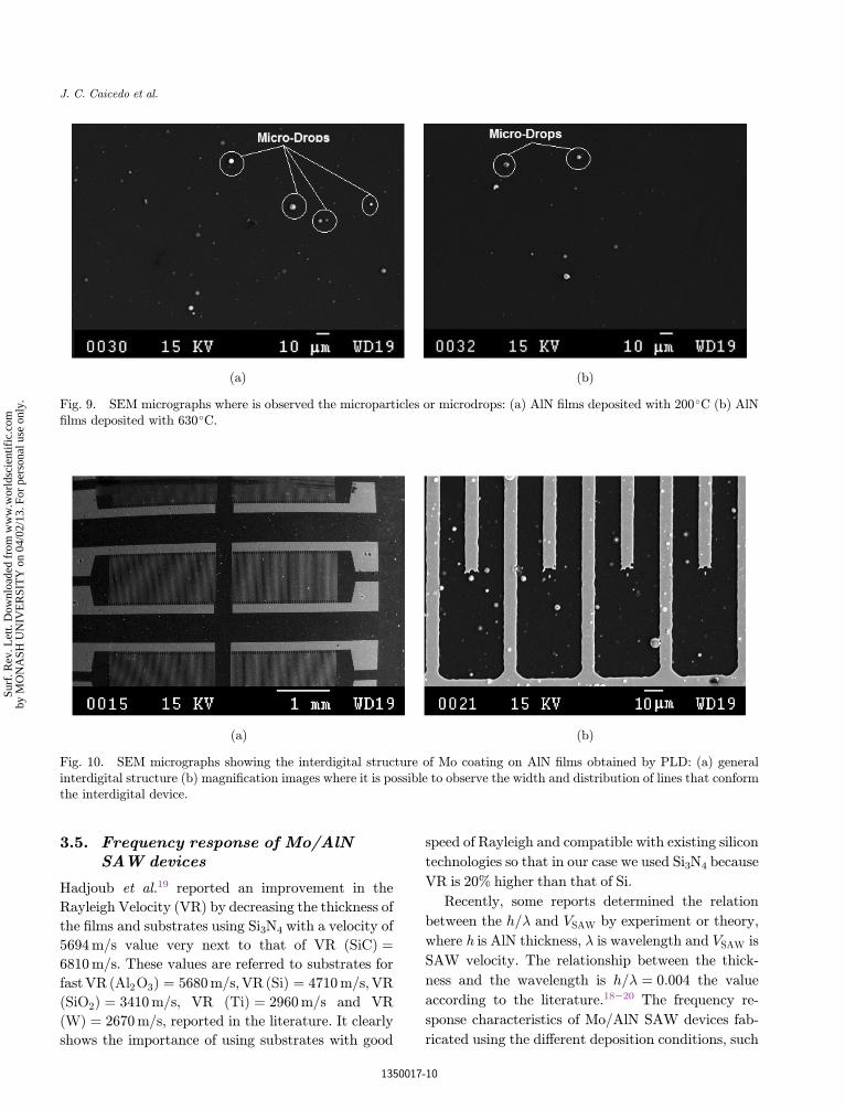
clearly a®ects the reduction of microdrops; this can
be possible due to great surface mobility when the
temperature was varied from 200�C to 630�C. Thissurface mobility reduces the possibility that the
microdrops are anchored on the surface when they
arrive with high energy on AlN ¯lm. Other possible
reason can be associated with high super¯cial tem-
perature that produces surface di®usion of micro-
particles or microdrops, which can decrease the
overall number of particles. A typical image is given
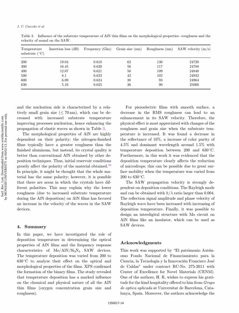
in Fig. 9(a). The magni¯cation image showed in
Fig. 10(b) exhibits that Mo lines are continuous,
without any interruption or short circuit. After
electrical measurements, it was possible to deduce an
insulator behavior for our AlN structures, a good
prerequisite for using them as SAW (Mo/AlN/SAW)
devices.
200 250 300 350 400 450 500 550 600 6500,625
0,630
0,635
0,640
0,645
0,650
0,655
0,660
0,665
Pure aluminium (0.90)
Co
lor
pu
rity
Deposition temperature (°C)
AlN films
(a)
200 250 300 350 400 450 500 550 600 650561
562
563
564
565
566
567
568
569
570
571
Pure aluminum 574 (nm)
Do
min
an
t w
av
ele
ng
th (
nm
)
Deposition temperature (°C)
AlN films
(b)
Fig. 8. Temperature dependence at color results for AlN ¯lms: (a) color purity and (b) dominant wavelength as function ofdeposition temperature.
Table 2. Optical properties for AlN ¯lms deposited onto Si3N4 substrate.
Deposition temperature (�C) Dominant wavelength (nm) Color purity Axis X Axis Y
200 562 0.63 0.234 0.121300 567 0.63 0.242 0.123400 569 0.63 0.240 0.132500 569 0.64 0.246 0.137600 569 0.65 0.262 0.158630 570 0.66 0.302 0.270Reference Aluminum 574 0.90 0.358 0.371
Determination of Physical Response in (Mo/AlN) SAW Devices
1350017-9
Surf
. Rev
. Let
t. D
ownl
oade
d fr
om w
ww
.wor
ldsc
ient
ific
.com
by M
ON
ASH
UN
IVE
RSI
TY
on
04/0
2/13
. For
per
sona
l use
onl
y.
3.5. Frequency response of Mo/AlNSAW devices
Hadjoub et al.19 reported an improvement in the
Rayleigh Velocity (VR) by decreasing the thickness of
the ¯lms and substrates using Si3N4 with a velocity of
5694m/s value very next to that of VR ðSiCÞ ¼6810m/s. These values are referred to substrates for
fastVR ðAl2O3Þ ¼ 5680m/s,VR ðSiÞ ¼ 4710m/s,VR
ðSiO2Þ ¼ 3410m/s, VR ðTiÞ ¼ 2960m/s and VR
ðWÞ ¼ 2670m/s, reported in the literature. It clearly
shows the importance of using substrates with good
speed of Rayleigh and compatible with existing silicon
technologies so that in our case we used Si3N4 because
VR is 20% higher than that of Si.
Recently, some reports determined the relation
between the h=� and VSAW by experiment or theory,
where h is AlN thickness, � is wavelength and VSAW is
SAW velocity. The relationship between the thick-
ness and the wavelength is h=� ¼ 0:004 the value
according to the literature.18�20 The frequency re-
sponse characteristics of Mo/AlN SAW devices fab-
ricated using the di®erent deposition conditions, such
(a) (b)
Fig. 9. SEM micrographs where is observed the microparticles or microdrops: (a) AlN ¯lms deposited with 200�C (b) AlN¯lms deposited with 630�C.
(a) (b)
Fig. 10. SEM micrographs showing the interdigital structure of Mo coating on AlN ¯lms obtained by PLD: (a) generalinterdigital structure (b) magni¯cation images where it is possible to observe the width and distribution of lines that conformthe interdigital device.
J. C. Caicedo et al.
1350017-10
Surf
. Rev
. Let
t. D
ownl
oade
d fr
om w
ww
.wor
ldsc
ient
ific
.com
by M
ON
ASH
UN
IVE
RSI
TY
on
04/0
2/13
. For
per
sona
l use
onl
y.

as, 200�C, 400�C and 630�C, have been measured
and results are shown in Figs. 11(a)�11(d). By using
the AlN bu®er layers, as can be seen by comparing
the wide-frequency scan spectra of those three devices
[which are plotted in the inserts of Fig. 11(c)], the
center frequency was shifted from approximately
0.618GHz [see Fig. 11(a)] to higher frequencies of
0.621GHz [see Fig. 11(b)] and 0.625GHz [see Fig. 11
(c)]. This indicates that the AlN bu®er layer could be
used as high phase-velocity substrate in the fabrica-
tion of high-frequency SAW devices, as with Mo.
In this research using di®erent deposition tem-
peratures of AlN bu®er the insertion loss was reduced.
When using the AlN bu®er layers, the center fre-
quency was shifted from approximately 0.618 [see
Fig. 11(a)] to 0.621GHz [see Fig. 11(b)] and
0.625GHz [see Fig. 11(c)]. This indicates that the
AlN bu®er layer could be used as a high phase
velocity substrate in the fabrication of high-frequency
SAW devices. Additionally, Fig. 11(c) shows that
using AlN bu®er reduced the insertion loss. To ex-
amine in more detail the dependence of insertion loss
0,50 0,55 0,60 0,65 0,70-40
-35
-30
-25
-20
-15
-10
-5
Ins
ert
ion
Lo
ss
(d
B)
Frequency (GHz)
200 °C
-19.04 (dB)
(a)
0,50 0,55 0,60 0,65 0,70-40
-35
-30
-25
-20
-15
-10
-5
Ins
ert
ion
Lo
ss
(d
B)
Frequency (GHz)
400 °C
-12.07 (dB)
(b)
0,50 0,55 0,60 0,65 0,70-40
-35
-30
-25
-20
-15
-10
-5
Insert
ion
Lo
ss (
dB
)
Frequency (GHz)
630 °C
-5.16 (dB)
(c) (d)
Fig. 11. Frequency response characteristics of fabricated Mo/AlN SAW devices with di®erent deposition temperatures (a)200�C (b) 400�C (c) 630�C and (d) the insertion loss by the use di®erent deposition temperatures of AlN bu®er layer.
Determination of Physical Response in (Mo/AlN) SAW Devices
1350017-11
Surf
. Rev
. Let
t. D
ownl
oade
d fr
om w
ww
.wor
ldsc
ient
ific
.com
by M
ON
ASH
UN
IVE
RSI
TY
on
04/0
2/13
. For
per
sona
l use
onl
y.

on the deposition condition of AlN bu®er, the inser-
tion loss was measured for all fabricated SAW devices
as was shown for the frequency response superposi-
tion in Fig. 11(d).
The results are plotted in Fig. 12 as a function of
temperature deposition of AlN ¯lms and the esti-
mated quantitative values are also listed in Fig. 11.
As can be seen in Fig. 12, for SAW devices fabricated
using the sputtered-AlN bu®er with Mo channel the
insertion loss was exactly correlated with the corre-
sponding temperature value for all AlN ¯lms.
This can be identi¯ed by comparing the results
obtained from the device with AlN ¯lms deposited on
silicon nitride substrate. For the aforementioned
devices, the temperature deposition was increasing
systematically, as already shown in Fig. 12. More-
over, the device with AlN deposited to 630�Crevealed the relatively large insertion loss in relation
to frequency value (0.625GHz). This may be attrib-
uted to the relatively low surface roughness (90 nm)
AlN ¯lm used in Mo/AlN device considering that the
surface roughness of AlN ¯lm may also be a®ected by
the surface morphology and deposition temperature
of AlN bu®er layer,21 the results shown in Fig. 11(d)
con¯rm that frequency response characteristics (in-
sertion loss) can be a®ected by reduction of oxygen
concentration, reduction of grain size, roughness and
decreasing with re°ectance of AlN ¯lms together with
increase of color purity and dominant wavelength. In
this sense, the property of AlN bu®er may strongly
govern the characteristic of SAW device using the
Mo/AlN system.
B�en�edic et al.22 reported the direct relationship
between increased frequency and speed in SAW
devices. All this is related to the morphological
qualities of roughness and grain size favor in in-
creased rate of velocity. Therefore, the resonance
frequency of a SAW is determined by the equation
f ¼ V =k, where f is the resonance frequency, V is
the phase velocity of the acoustic wave and K is the
acoustic wavelength, which in turn is de¯ned by the
electrode pitch in the IDT. The re°ected signal of
the Rayleigh mode in AlN ¯lms deposited to highest
temperatures (630�C) is observed to be much
stronger than that of the AlN ¯lms deposited to
lowest temperatures (200�C) and the phase velocity
of AlN ¯lms deposited to (630�C) is much higher.
For The Mo/AlN SAW devices, the measured reso-
nant frequencies of the Rayleigh mode waves ranges
from 0.618 to 0.625GHz corresponding to phase
velocities of 24720 to 25000m/s, indicating good re-
peatability and reproducibility.23�25 Thus, the lower
deposition temperature of the substrate generates a
perturbation of the acoustic velocity that is related
to a change in frequency of the oscillator circuit.
Figure 13 shows improvement of velocity with in-
creased temperature of the ¯lms deposited during the
growth of AlN and was used as substrates for SAW
devices building Mo metal.
Taking into account the last behavior, it is possi-
ble to observe that the quasi-static electric ¯eld
200 300 400 500 600 700-22
-20
-18
-16
-14
-12
-10
-8
-6
-4
0.624 (GHz)0.623 (GHz)
0.620 (GHz)
0.625 (GHz)
0.621 (GHz)
Ins
ert
ion
Lo
ss
(d
B)
Temperature (°C)
Mo/AlN SAW
0.618 (GHz)
Fig. 12. The measured insertion losses of fabricated Mo/AlN SAW devices, as a function of the temperature valuesfrom the deposited AlN ¯lms.
200 300 400 500 600 70024700
24750
24800
24850
24900
24950
25000
25050
Ve
loc
ity
(m
/s)
Temperature (°C)
0.624 (GHz)0.623 (GHz)
0.620 (GHz)
0.625 (GHz)
0.621 (GHz)
Mo/AlN SAW
0.618 (GHz)
Fig. 13. Acoustic wave velocity as a function of depositiontemperature in Mo/AlN/Si3N4 system.
J. C. Caicedo et al.
1350017-12
Surf
. Rev
. Let
t. D
ownl
oade
d fr
om w
ww
.wor
ldsc
ient
ific
.com
by M
ON
ASH
UN
IVE
RSI
TY
on
04/0
2/13
. For
per
sona
l use
onl
y.

associated with the SAW interacts with the charge
carriers of the ¯lm. The SAW velocity is, therefore,
dependent on the AlN thin ¯lm conductivity changes.
These velocity changes can easily be interpreted as a
shift in the resonant frequency, when the SAW delay
line is incorporated in an oscillator con¯guration. The
e®ect of temperature is one of the easiest parameters
that can be sensed because almost all physical and
chemical e®ects depend on temperature.26
In certain applications, the e®ect of temperature
should be minimized in order to avoid any interfer-
ence with other e®ects. For acoustic wave sensors, the
temperature e®ect induces dimensional dilatations
and small changes in the mechanical and electrical
properties. Two kinds of interaction can thus be
measured: (i) shift of the acoustic wave velocity due
to intrinsic changes of material properties (elasticity,
density, etc) this is the case for almost all SAW
devices using metal-nitrides materials with low
thickness27 and (ii) for acoustic devices for which the
resonant frequency or the velocity is dependent on the
dimensional values (Lamb wave devices, thickness
shear mode, etc.), temperature can a®ect changes of
both material properties and boundary conditions.28
3.6. Correlation between opticalproperties and acoustic wave velocityin Mo/AlN SAW devices
Figure 14(a) shows the relationship between optical
properties (re°ectance), acoustic wave velocity and
deposition temperature in AlN ¯lms. In this research,
it is clearly shown that, when the deposition tem-
perature decreases, reduction of grain size (see Fig. 5),
reduction of re°ectance [see Fig. 7(b)] and the in-
crease of the color purity [see Fig. 8(a)] is associated
with an increase of frequency response (see Fig. 13)
due to the increase of acoustic wave velocity (see
Fig. 13) produced by energy activation at higher de-
position temperatures. From this correlation, it is
possible to determine that the two-merit index29
associates to an acceptable re°ectance with accept-
able acoustic wave velocity at the same temperature
deposition, and it also associates to an acceptable
roughness with acceptable acoustic wave velocity at
the same temperature deposition.
Therefore, theAlN¯lms deposited between 400 and
500�C o®er the best synergy for optical and acoustic
properties with good re°ectance and an acceptable
acoustic wave velocity. Moreover, AFM results in
Fig. 14(b) show a direct relationship between the de-
crease in roughness of the AlN thin ¯lms and the in-
crease of the deposition temperature.
In this research, is shown a clear correlation is
shown between the roughness and the Rayleigh ve-
locity. At lower roughness the highest velocity is
obtained for the samples grown at a higher temper-
ature of 630�C. Therefore, the AlN ¯lms deposited
around 450�C o®er the best synergy for optical and
acoustic properties with good re°ectance and an ac-
ceptable acoustic wave velocity. Furthermore, the
nanometric grain size and in thickness of such thin
¯lms AlN/Si3N4 a low surface roughness (� 120 nm)
200 250 300 350 400 450 500 550 600 650 70020
22
24
26
28
30
32
34
36
24650
24700
24750
24800
24850
24900
24950
25000
25050Re(%)
Wavelength 760 - 800 (nm)
Re
fle
cta
nc
e (
%)
Deposition temperature (°C)
Mo/AlN/Si SAW
V(m/s)
Ve
loc
ity
(m
/s)
(a)
200 250 300 350 400 450 500 550 600 650 700
70
80
90
100
110
120
130
140
VelocityRoughness
Deposition temperature (°C)
Ro
ug
hn
es
s (
nm
)
24700
24750
24800
24850
24900
24950
25000
25050
25100
Ve
loc
ity
(m
/s)
(b)
Fig. 14. Correlation between optical, morphological andacoustic properties with the deposition temperature: (a)correlation between optical properties (Re°ectance) andacoustic wave velocity in Mo/AlN SAW devices and (b)correlation between roughness and Rayleigh velocity as afunction of temperature deposit AlN thin ¯lms.
Determination of Physical Response in (Mo/AlN) SAW Devices
1350017-13
Surf
. Rev
. Let
t. D
ownl
oade
d fr
om w
ww
.wor
ldsc
ient
ific
.com
by M
ON
ASH
UN
IVE
RSI
TY
on
04/0
2/13
. For
per
sona
l use
onl
y.
and the nucleation side is characterized by a rela-
tively small grain size (� 70 nm), which can be de-
creased with increased substrate temperature
improving processes nucleation, hence enhancing the
propagation of elastic waves as shown in Table 3.
The morphological properties of AlN are highly
dependent on their polarity; the nitrogen-¯nished
¯lms typically have a greater roughness than the
¯nished aluminum, but instead, its crystal quality is
better than conventional AlN obtained by other de-
position techniques. Thus, initial reservoir conditions
greatly a®ect the polarity of the material obtained.30
In principle, it might be thought that the whole ma-
terial has the same polarity; however, it is possible
that there are areas in which the crystals have dif-
ferent polarities. This may explain why the lower
roughness (due to increased substrate temperature
during the AlN deposition) on AlN ¯lms has favored
an increase in the velocity of the waves in the SAW
devices.
4. Summary
In this paper, we have investigated the role of
deposition temperature in determining the optical
properties of AlN ¯lms and the frequency response
characteristics of Mo/AlN/Si3N4 SAW devices.
The temperature deposition was varied from 200 to
630�C to analyze their e®ect on the optical and
morphological properties of the ¯lms. XPS con¯rmed
the formation of the binary ¯lms. The study revealed
that temperature deposition has a marked in°uence
on the chemical and physical nature of all the AlN
thin ¯lms (oxygen concentration grain size and
roughness).
For piezoelectric ¯lms with smooth surface, a
decrease in the RMS roughness can lead to an
enhancement in its SAW velocity. Therefore, the
physical e®ect is most appreciated with changes of the
roughness and grain size when the substrate tem-
perature is increased. It was found a decrease in
the re°ectance of 10%, a increase of color purity of
4.5% and dominant wavelength around 1.5% with
temperature deposition between 200 and 630�C.Furthermore, in this work it was evidenced that the
deposition temperature clearly a®ects the reduction
of microdrops; this can be possible due to great sur-
face mobility when the temperature was varied from
200 to 630�C.The SAW propagation velocity is strongly de-
pendent on deposition conditions. The Rayleigh mode
and can be obtained with h=� ratio larger than 0.004.
The re°ection signal amplitude and phase velocity of
Rayleigh wave have been increased with increasing of
deposition temperature. Finally, it was possible to
design an interdigital structure with Mo circuit on
AlN ¯lms like an insulator, which can be used as
SAW devices.
Acknowledgments
This work was supported by \El patrimonio Autón-omo Fondo Nacional de Financiamiento para la
Ciencia, la Tecnología y la Innovación Francisco Jos�e
de Caldas" under contract RC-No. 275-2011 with
Center of Excellence for Novel Materials (CENM).
One of the authors, H. R, wishes to express his grati-
tude for the kind hospitality o®ered to him fromGrupo
de optica aplicada at Universitat de Barcelona, Cata-
lunya, Spain. Moreover, the authors acknowledge the
Table 3. In°uence of the substrate temperature of AlN thin ¯lms on the morphological properties�roughness and thevelocity of sound on the SAW.
Temperaturesubstrate (�C)
Insertion loss (dB) Frequency (Ghz) Grain size (nm) Roughness (nm) SAW velocity (m/s)
200 19.04 0.618 62 130 24720300 16.45 0.620 56 117 24788400 12.07 0.621 50 109 24840500 8.1 0.623 42 102 24932600 6.09 0.624 38 93 24964630 5.16 0.625 36 90 25000
J. C. Caicedo et al.
1350017-14
Surf
. Rev
. Let
t. D
ownl
oade
d fr
om w
ww
.wor
ldsc
ient
ific
.com
by M
ON
ASH
UN
IVE
RSI
TY
on
04/0
2/13
. For
per
sona
l use
onl
y.

Serveis Cientí¯co-T�ecnics of the Universitat de Bar-
celona for and XPS, SEM and optical analysis.
References
1. C. Men and C. Lin,Mater. Sci. Eng. B 133 (2006) 124.2. C. Ristoscu, C. Ducu, G. Socol, F. Craciunoiu and I. N.
Mihailescu, Appl. Surf. Sci. 248 (2005) 411.3. H. Yamashita, K. Fukui, S. Misawa and S. Yoshida,
J. Appl. Phys. 50 (1979) 896.4. N. E. Christensen and I. Gorczyca, Phys. Rev. B 50
(1994) 4397.5. J. L. P. Hughes, Y. Wang and J. E. Sipe, Phys. Rev. B
55 (1997) 13630.6. L. F. Jiang, W. Z. Shen, H. Ogawa and Q. X. Guo,
J. Appl. Phys. 94 (2003) 5704.7. M. Clement, L. Vergara, J. Sangrador, E. Iborra and
A. Sanz-Herv�as, Ultrasonics 42 (2004) 403.8. J. A. P�erez, H. Riascos, J. C. Caicedo, G. Cabrera and
L. Yate, J. Phys.: Conf. Ser. 274 (2011) 012119.9. L. Rosenberger, R. Baird, E. McCullen, G. Auner and
G. Shreve, Surf. Interface Anal. 40 (2008) 12541261.10. C. Zhuang, J. Zhao, F. Jia, C. Guan, Z. Wu, Y. Bai
and X. Jiang, Surf. Coat Technol. 204 (2009) 713.11. P. W. Wang, S. Sui, W. Wang and W. Durrer, Thin
Solid Films 295 (1997) 142.12. V. Brien and P. Pigeat, J. Cryst. Growth 299 (2007)
189.13. A. M. Mahmood, R. Machorro, J. Heiras, F. F.
Catrillon, M. H. Farias and E. Andrade, Diam. Relat.Mater. 12 (2003) 1315.
14. J. A. P�erez et al., Neogranadina Sci. Eng. 20 (2010)107.
15. P. M. Raole, S. Mukherjee and P. I. John, Diam. Relat.Mater. 14 (2005), 482�485.
16. M. Bass, E. W. Van Stryland, (eds.) Handbook ofOptics (2nd ed.) Vol. 2, (McGraw-Hill, 1994).
17. H. A. Macleod, Thin-¯lm Optical Filters, 3rd Edn.(CRC Press, 2001), pp. 158�159.
18. N. S. Zayats, V. G. Boĭko, P. A. Gentsar, O. S. Litvin,V. P. Papusha and N. V. Sopinskiĭ, Semiconductors42-2 (2008) 195.
19. I. Touati, Z. Hadjoub and A. Doghmane, Phys. Chem.News 27 (2006) 26.
20. S. Niyomsoan, W. Grant, D. L. Olson and B. Mishra,Thin Solid Films 415 (2002) 187.
21. J.-P. Jung, J.-B. Lee, J.-S. Kim and J.-S. Park, ThinSolid Films 447{448 (2004) 605.
22. F. B�en�edic, M. B. Assouar, F. Mohasseb, O. Elmazria,P. Alnot and A. Gicquel, Diam. Relat. Mater. 13(2004) 347.
23. K.-Y. Hashimoto and M. Yamaguchi, IEEE Trans.Ultrason. Ferroelect. Freq. Control 48 (2001) 1181.
24. J. Kondoh and S. Shiokawa, Commun. Japan II 76(1993) 69.
25. J. Kondoh and S. Shiokawa Liquid identi¯cationusingSH-SAW sensors Transducers'95 The 8th Int.Conf. Solid-State Sensors and Actuators EurosensorsIX. Stockholm, 1995, pp. 716�719.
26. M. Hoummad, A. Campitelliand and W. Wlodarski,Smart Mater. Struct. 6 (1997) 647.
27. R. Bechmann, A. D. Ballato and T. J. Lukaszek, Proc.IRE 50 (1962) 1812.
28. M. Hoummady and D. Hauden, Sens. Actuators A 44(1994) 177.
29. J. C. Caicedo, G. Zambrano, W. Aperador, L. Escobar-Alarcon and E. Camps, Appl. Surf. Sci. 258 (2011)312.
30. Q. S. Paduano, D. W. Weyburne, J. Jasinski and Z.Liliental-Weber, J. Cryst. Growth 261 (2004) 259.
Determination of Physical Response in (Mo/AlN) SAW Devices
1350017-15
Surf
. Rev
. Let
t. D
ownl
oade
d fr
om w
ww
.wor
ldsc
ient
ific
.com
by M
ON
ASH
UN
IVE
RSI
TY
on
04/0
2/13
. For
per
sona
l use
onl
y.