The Multivalley Effective Conduction Band-Edge Method for Monte Carlo Simulation of Nanoscale...
8
IEEE TRANSACTIONS ON ELECTRON DEVICES, VOL. 53, NO. 11, NOVEMBER 2006 2703 The Multivalley Effective Conduction Band-Edge Method for Monte Carlo Simulation of Nanoscale Structures Carlos Sampedro-Matarín, Francisco Gámiz, Senior Member, IEEE, Andrés Godoy, and Francisco J. García Ruiz Abstract—The trend toward continuous integration of the nanometer scale and the rise of nonconventional device con- cepts such as multigate transistors present important challenges for the semiconductor community. Simulation tools have to be adapted to this new scenario where classical approaches are not sufficiently accurate, and quantum effects have to be taken into account. This paper proposes a method of including quantum corrections in Monte Carlo (MC) simulations without solving the Schrödinger equation. The approach, based on the effective conduction band-edge (ECBE) method, considers the effects of an arbitrary effective mass tensor, describing valley characteristics and confinement directions while avoiding the use of effective mass as a fitting parameter. The performance of the multivalley ECBE method is tested using an ensemble MC simulator to study benchmark devices for next International Technology Roadmap for Semiconductors technological nodes, a 25-nm channel length bulk-MOSFET and a double-gate silicon-on-insulator MOSFET in both steady-state and transient situations. Index Terms—Monte Carlo (MC) methods, MOSFETs, quan- tum well, semiconductor device modeling, silicon-on-insulator (SOI) technology. I. INTRODUCTION F ROM THE point of view of integration, there is a con- stant trend in the semiconductor industry toward achieving faster operation and lower power consumption. Silicon-on- insulator (SOI) devices are the best solution to resolve the problems that appear when the size of the device is reduced to a few nanometers, due to their immunity to short channel effects (SCEs) and the reduction in junction capacitance. These characteristics allow a higher frequency of operation for a given voltage supply or a lower power consumption for a given frequency compared to traditional CMOS devices [1]. This technology also offers the possibility of nonconventional device concepts such as multigate transistors providing new ways of improving device performance. The reduction in the critical size of the devices implies a significant increase in manufacturing costs, especially now, when high performance and low-power consumption products in the nanometer range Manuscript received May 23, 2006. The review of this paper was arranged by Editor M. Reed. The authors are with the Departamento de Electrónica y Tecnología de Computadores, Universidad de Granada, 18071 Granada, Spain (e-mail: [email protected]). Color versions of Figs. 2–6, 8–10, 12, and 13 are available online at http://ieeexplore.ieee.org. Digital Object Identifier 10.1109/TED.2006.882782 exist. Therefore, great efforts should be made in “a priori” device optimization, using simulation tools in order to reduce design costs. Classical drift-diffusion simulators are still widely used although the models needed to fit experimental results are more complex, including nonphysically based parameters which can be justified only because experimental curves are well reproduced. At the other end of the spectrum, full quantum simulators based on the solution of the Schrödinger equation or the non-equilibrium green’s functions theory (NEGF) have also been developed [2] but such codes are very time consuming from the computational point of view and have a limited ap- plicability since the inclusion of a comprehensive set of scatter- ing mechanisms and actual device geometry is limited. Between these extreme approaches, semiclassical simulators including quantum corrections have several advantages such as a reduced computational cost, the possibility of considering a wide variety of scattering mechanisms, and high accuracy for devices with silicon thicknesses down to 4 nm [3]. Ensemble Monte Carlo (EMC) simulators have been widely used, adding a quantum term in order to correct the electrostatic potential resulting from the classical solution of Poisson’s equation to mimic the electron concentration profile obtained when the Schrödinger equation is solved. The calibration of such corrections is not free from fitting parameters (e.g., carrier effective mass in the density gradient model) but the results obtained are still accurate from the transport point of view. We have developed an extension of one of these methods known as the effective conduction band-edge (ECBE) model, considering the effects of an arbitrary effective mass tensor describing valley char- acteristics and confinement directions where effective masses are not used as a fitting parameter, as in the standard version. This approximation is implemented in a quantum-corrected MC (QMC) simulator, which includes new models to describe electron–phonon interaction and surface-roughness scattering based on two-dimensional (2-D) electron gas mechanisms. Mobility calculations performed in long channel devices have been used to calibrate the scattering parameters with simula- tions carried out using a one-particle one-dimensional (1-D) MC simulator which self-consistently solves Poisson and Schrödinger equations. The QMC is then tested in two de- vices that have fulfilled International Technology Roadmap for Semiconductors (ITRS) 2004 [4] specifications for next nodes including steady-state simulations, to compare quantum and classical results and transient studies. This paper is divided as follows: In Section II, different methods of including quantum 0018-9383/$20.00 © 2006 IEEE
Transcript of The Multivalley Effective Conduction Band-Edge Method for Monte Carlo Simulation of Nanoscale...

IEEE TRANSACTIONS ON ELECTRON DEVICES, VOL. 53, NO. 11, NOVEMBER 2006 2703
The Multivalley Effective Conduction Band-EdgeMethod for Monte Carlo Simulation of
Nanoscale StructuresCarlos Sampedro-Matarín, Francisco Gámiz, Senior Member, IEEE, Andrés Godoy, and Francisco J. García Ruiz
Abstract—The trend toward continuous integration of thenanometer scale and the rise of nonconventional device con-cepts such as multigate transistors present important challengesfor the semiconductor community. Simulation tools have to beadapted to this new scenario where classical approaches are notsufficiently accurate, and quantum effects have to be taken intoaccount. This paper proposes a method of including quantumcorrections in Monte Carlo (MC) simulations without solvingthe Schrödinger equation. The approach, based on the effectiveconduction band-edge (ECBE) method, considers the effects of anarbitrary effective mass tensor, describing valley characteristicsand confinement directions while avoiding the use of effectivemass as a fitting parameter. The performance of the multivalleyECBE method is tested using an ensemble MC simulator to studybenchmark devices for next International Technology Roadmapfor Semiconductors technological nodes, a 25-nm channel lengthbulk-MOSFET and a double-gate silicon-on-insulator MOSFETin both steady-state and transient situations.
Index Terms—Monte Carlo (MC) methods, MOSFETs, quan-tum well, semiconductor device modeling, silicon-on-insulator(SOI) technology.
I. INTRODUCTION
FROM THE point of view of integration, there is a con-stant trend in the semiconductor industry toward achieving
faster operation and lower power consumption. Silicon-on-insulator (SOI) devices are the best solution to resolve theproblems that appear when the size of the device is reducedto a few nanometers, due to their immunity to short channeleffects (SCEs) and the reduction in junction capacitance. Thesecharacteristics allow a higher frequency of operation for agiven voltage supply or a lower power consumption for agiven frequency compared to traditional CMOS devices [1].This technology also offers the possibility of nonconventionaldevice concepts such as multigate transistors providing newways of improving device performance. The reduction in thecritical size of the devices implies a significant increase inmanufacturing costs, especially now, when high performanceand low-power consumption products in the nanometer range
Manuscript received May 23, 2006. The review of this paper was arrangedby Editor M. Reed.
The authors are with the Departamento de Electrónica y Tecnologíade Computadores, Universidad de Granada, 18071 Granada, Spain (e-mail:[email protected]).
Color versions of Figs. 2–6, 8–10, 12, and 13 are available online athttp://ieeexplore.ieee.org.
Digital Object Identifier 10.1109/TED.2006.882782
exist. Therefore, great efforts should be made in “a priori”device optimization, using simulation tools in order to reducedesign costs. Classical drift-diffusion simulators are still widelyused although the models needed to fit experimental resultsare more complex, including nonphysically based parameterswhich can be justified only because experimental curves arewell reproduced. At the other end of the spectrum, full quantumsimulators based on the solution of the Schrödinger equation orthe non-equilibrium green’s functions theory (NEGF) have alsobeen developed [2] but such codes are very time consumingfrom the computational point of view and have a limited ap-plicability since the inclusion of a comprehensive set of scatter-ing mechanisms and actual device geometry is limited. Betweenthese extreme approaches, semiclassical simulators includingquantum corrections have several advantages such as a reducedcomputational cost, the possibility of considering a wide varietyof scattering mechanisms, and high accuracy for devices withsilicon thicknesses down to 4 nm [3]. Ensemble Monte Carlo(EMC) simulators have been widely used, adding a quantumterm in order to correct the electrostatic potential resultingfrom the classical solution of Poisson’s equation to mimic theelectron concentration profile obtained when the Schrödingerequation is solved. The calibration of such corrections is notfree from fitting parameters (e.g., carrier effective mass inthe density gradient model) but the results obtained are stillaccurate from the transport point of view. We have developedan extension of one of these methods known as the effectiveconduction band-edge (ECBE) model, considering the effectsof an arbitrary effective mass tensor describing valley char-acteristics and confinement directions where effective massesare not used as a fitting parameter, as in the standard version.This approximation is implemented in a quantum-correctedMC (QMC) simulator, which includes new models to describeelectron–phonon interaction and surface-roughness scatteringbased on two-dimensional (2-D) electron gas mechanisms.Mobility calculations performed in long channel devices havebeen used to calibrate the scattering parameters with simula-tions carried out using a one-particle one-dimensional (1-D)MC simulator which self-consistently solves Poisson andSchrödinger equations. The QMC is then tested in two de-vices that have fulfilled International Technology Roadmap forSemiconductors (ITRS) 2004 [4] specifications for next nodesincluding steady-state simulations, to compare quantum andclassical results and transient studies. This paper is divided asfollows: In Section II, different methods of including quantum
0018-9383/$20.00 © 2006 IEEE

2704 IEEE TRANSACTIONS ON ELECTRON DEVICES, VOL. 53, NO. 11, NOVEMBER 2006
corrections in device simulators are discussed and one of these,the ECBE, is used as a starting point to develop a multivalley(MV) version to be used in EMC codes. Section III refers tothe features and implemented scattering models of the devicesimulator used to perform the calculations. The main character-istics and the geometry of the devices being studied are shownin Section IV. Section V presents the results obtained withthe simulator and finally, in Section VI, the main conclusionsare drawn.
II. ECBE METHOD
One way to include quantum corrections in a semiclassicalEMC simulator without solving the Schrödinger equation is bythe addition of a correction term to the electrostatic potential toreproduce the carrier density given by the full quantum solution.The following two approaches are those most commonly used.
1) The effective potential model [5] where the correctionto the classical potential is obtained from the convolu-tion of the potential and a Gaussian function which rep-resents the “effective size” of the particle. The 1-D formof the correction is given by
Veff(x) =1√
2πa0
∫V (x′) exp
(− (x− x′)2
2a20
)dx′ (1)
where V (x′) is the classical potential and a0 representsthe spreading of the wave packet. This approximationshifts the maximum electron distribution from the ox-ide interfaces reproducing the inversion charge valuebut resulting in an incorrect carrier density profile [6].The method is not appropriate when magnitudes whichdepend on the overlapping integral, involving envelopefunctions extracted from carrier distributions, need to becalculated, as may be the case with surface-roughnessmodels or intervalley scattering rates when size quanti-zation is taken into account.
2) The density gradient method [7] which uses the Wignerpotential and produces very good results, especially indrift-diffusion simulations. The proposed correction termis given by
Vq = 2bn∇2(√n)√
n(2)
where bn = �2/4rm∗n, � is the Planck’s constant divided
by 2π, m∗n represents the electron effective mass, and r isa parameter whose value varies from 1 for pure states (lowtemperatures or very strong confinement) to 3 for mixedstates (high temperatures or weak confinement). Thiscorrection is not easily implemented in MC simulationsdue to the fact that the driving force depends on the thirdderivative of the electron concentration, which is a verynoisy magnitude. To avoid this problem, the quantumcorrection should be expressed in terms of electrostaticpotential. The ECBE exploits this idea [8].
Starting from the density gradient, (2), and assuming anexponential relation between the electron concentration and theeffective potential, n ∝ exp(qV ∗/kBT ), V ∗ can be written as
V ∗ = V + Vq = V +q�2
4rm∗nkBT
(∇2V ∗ +
q
2kBT(∇V ∗)2
).
(3)
This equation has to be self-consistently solved with Poissonand Boltzmann transport equations (BTEs) using the boundaryconditions proposed by [9]. The effective mass is used as afitting parameter, agreeing well with a self-consistent solutionof the 1-D Poisson–Schrödinger equations when the electronconcentration profiles are compared. This change in the valueof the mass is due to the fact that the valley occupation dependson the bias point and this model only considers one valley. Adeeper discussion about the limitations of this approach can befound elsewhere [8].
The main goal of this paper is to develop a new expressionto take into account the electron population in different valleysand an arbitrary orientation in order to avoid using the effectivemass as a fitting parameter. To do so, let us consider the one-particle Schrödinger equation representing the effective mass asa tensor
−�2
2∇ ·
(←→
1m
)j
∇Ψj
+ U(�r )Ψj = i�
∂Ψj
∂t(4)
where the subindex j represents the valley. Assuming that thewave function can be written as follows
Ψj = Rj exp(iSj
�
)(5)
where Rj and Sj are the modulus and phase of the solution,respectively; when we substitute (5) in (4), the following ex-pressions for the imaginary and real parts of the solution are,respectively, obtained
∂Pj
∂t+∇ ·
(←→
1m
)j
· (Pj · ∇Sj)
= 0 (6)
− �2
2Rj∇ ·
(←→
1m
)j
· ∇Rj
+
12∇Sj ·
(←→
1m
)j
· ∇Sj
+ U(�r ) = −∂Sj
∂t(7)
where Pj = R2j . Assuming pure states (Pj(�r ) ∝ nj(�r )) sta-
tionary conditions (Sj = −Ejt + cons) and small currentregime, (7) becomes
Ej = U(�r )− �2
2√nj∇ ·
(←→
1m
)j
· ∇√nj
. (8)
SAMPEDRO-MATARÍN et al.: MV-ECBE METHOD FOR MC SIMULATION OF NANOSCALE STRUCTURES 2705
If we consider a semiclassical expression supposing con-tinuous energy, (8) can be written as
V ∗j = V +�
2
2q√nj∇ ·
(←→
1m
)j
· ∇√nj
(9)
where Ej = −qV ∗j , U(�r ) = −qV with V the electrostatic po-tential obtained from Poisson’s equation, which is the generalexpression for the density gradient theory considering multiplevalleys and arbitrary confinement directions.
To obtain the final expression of the MV-ECBE approxi-mation, let us suppose an exponential form of the electronconcentration
nj ∝ exp(V ∗jVT
)(10)
where VT = kBT/q is the thermal potential. Substituting (10)in (9) and considering the mixed states correction via the rparameter, the final expression can be written as
V ∗j V +�
2
4qrVT
∇ ·
(←→
1m
)j
· ∇V ∗j
+1
2VT
∇V ∗j ·
(←→1m
)j
· ∇V ∗j
(11)
which is the ECBE equation for a MV system and arbitraryconfinement directions. It is easy to demonstrate that (11)reduces to the standard density gradient theory, (3), when onlyone valley and a diagonal effective mass tensor with the samevalue for all the elements are assumed. In the next sections,simulation results will be shown considering the three valleysin silicon and a diagonal mass tensor for (100), (110), and (111)surfaces.
III. DESCRIPTION OF THE QMC SIMULATOR
An EMC simulator has been used to solve the BTE self-consistently with Poisson’s equation. Quantum effects are in-cluded via the MV version of ECBE where (11) is solved foreach valley in the semiconductor that is considered (tunnelingis not taken into account).
This code is 2-D in real space and 3-D in k-space where timeis also considered as an independent variable for performingtransient simulations. Acoustic phonon and coulomb scatteringhave been included. Intervalley scattering has been imple-mented using zero order approximation with three differentphonons following the work in [10] where the mechanism wasadapted to the pseudo-2-D electron gas. To do this, scatteringrates are weighted by the overlapping integral between the ini-tial and final valley envelope functions, which are calculated bynormalizing the actual electron concentration for each valley. Inthis way, size quantization is taken into account and the valleypopulation is calculated self-consistently. Surface-roughnessscattering has been implemented using a three-dimensional(3-D) version of the model proposed by Gámiz et al. [11],
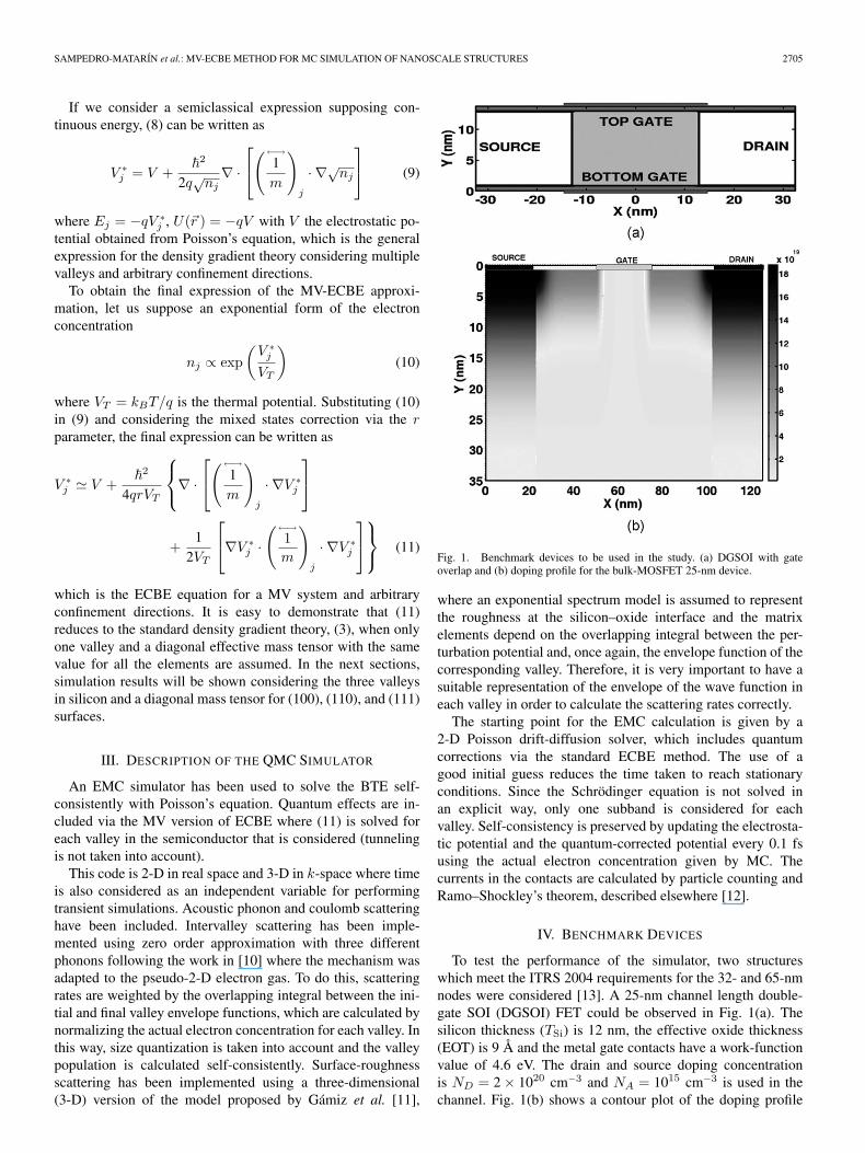
Fig. 1. Benchmark devices to be used in the study. (a) DGSOI with gateoverlap and (b) doping profile for the bulk-MOSFET 25-nm device.
where an exponential spectrum model is assumed to representthe roughness at the silicon–oxide interface and the matrixelements depend on the overlapping integral between the per-turbation potential and, once again, the envelope function of thecorresponding valley. Therefore, it is very important to have asuitable representation of the envelope of the wave function ineach valley in order to calculate the scattering rates correctly.
The starting point for the EMC calculation is given by a2-D Poisson drift-diffusion solver, which includes quantumcorrections via the standard ECBE method. The use of agood initial guess reduces the time taken to reach stationaryconditions. Since the Schrödinger equation is not solved inan explicit way, only one subband is considered for eachvalley. Self-consistency is preserved by updating the electrosta-tic potential and the quantum-corrected potential every 0.1 fsusing the actual electron concentration given by MC. Thecurrents in the contacts are calculated by particle counting andRamo–Shockley’s theorem, described elsewhere [12].
IV. BENCHMARK DEVICES
To test the performance of the simulator, two structureswhich meet the ITRS 2004 requirements for the 32- and 65-nmnodes were considered [13]. A 25-nm channel length double-gate SOI (DGSOI) FET could be observed in Fig. 1(a). Thesilicon thickness (TSi) is 12 nm, the effective oxide thickness(EOT) is 9 Å and the metal gate contacts have a work-functionvalue of 4.6 eV. The drain and source doping concentrationis ND = 2× 1020 cm−3 and NA = 1015 cm−3 is used in thechannel. Fig. 1(b) shows a contour plot of the doping profile

2706 IEEE TRANSACTIONS ON ELECTRON DEVICES, VOL. 53, NO. 11, NOVEMBER 2006
TABLE IVALUES USED IN THE EFFECTIVE MASS TENSORS FOR EACH VALLEY.X REPRESENTS THE TRANSPORT DIRECTION, Y THE CONFINEMENT
DIRECTION, AND Z IS PERPENDICULAR TO THE XY PLANE.ml = 0.91m0 AND mt = 0.19m0 ARE THE LONGITUDINAL
AND TRANSVERSAL EFFECTIVE MASSES RESPECTIVELY
(m0 IS THE FREE ELECTRON MASS)
Fig. 2. Cross section of electron density in the center of the channel in theDGSOI device with Tox = 0.9 nm when 1 V is applied to each gate. Poisson-Schrödinger solution (solid) is compared with MC results using the MV-ECBE(dashed). The contribution from each valley is also shown (symbols).
in the second device, a 25-nm channel length bulk nMOSFETwhere the gate contact is made of n-polysilicon, the oxidethickness is again 9 Å and Gaussian doping profiles are consid-ered including source/drain extensions and HALO diffusionsto reduce SCEs. The drain and source doping concentrationis ND = 2× 1020 cm−3 and NA = 3× 1018 cm−3 in thechannel.
Three surface orientations were considered for the DGSOIdevice and only the (100) in the case of the nMOSFET. Thevalues used in the effective mass tensors for each valley areshown in Table I, where X represents the transport direction,Y the confinement direction, and Z is perpendicular to the XYplane shown in Fig. 1. ml = 0.91m0 and mt = 0.19m0 are thelongitudinal and transversal effective masses, respectively, andm0 is the free electron mass.
V. SIMULATION RESULTS
A set of simulations were performed to compare classical andQMC codes. Fig. 2 shows the actual carrier distribution whenquantum corrections are taken into account at the midpointbetween drain and source of the DGSOI transistor for the (100)surface orientations with VG = 1 V and VDS = 0 V. Using the
Fig. 3. Detail of the electrostatic potential in a DGSOI MOSFET near theSi-SiO2 interface when 1 V is applied to both gates. Classical (solid) andquantum-corrected potentials used to calculate the driving force for each valleyin EMC simulations are represented. The repulsive potential can be observednear the interface (depth = 0.9 nm) for MV-ECBE calculations.
symmetry of the structure, only half the electron concentrationhas been represented. As can be observed, the maximum ofthe distribution is no longer at the interface and its positioncorresponds to that predicted by the solution of the Schrödingerequation (solid line). The MV-ECBE solution is sketched witha dashed line and the distributions corresponding to each valleyare represented by symbols. Valley number one corresponds tothe heaviest confinement mass, which is the most populated,as theory would lead us to expect, showing a break in thedegeneracy band minima compared to the 3-D electron gasmodel.
Since tunneling has not been taken into account in this paper,quantum corrections are calculated only in the silicon slabsandwiched between the oxide. Fig. 3 shows the electrostaticpotential (solid) and the corrected potential corresponding toeach valley, again for the (100) surface. A repulsive potentialcan be observed near the silicon–oxide interfaces pushing outthe electrons from the interface, however the quantum correc-tion tends toward zero where confinement effects are negligi-ble. The MV-ECBE introduces different corrections for eachvalley since the confinement effective masses are not the samefor each.
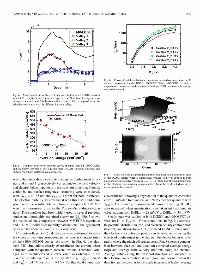
Fig. 4 shows a mid-channel electron concentration cut for thesame conditions as in Fig. 2 but when 1 V is applied betweendrain and source. In this case, the degeneration in valleys2 and 3, which have the same confinement mass, is broken whenan electric field is applied.
To calibrate the simulator in terms of transport, a set ofsimulations were performed to calculate mobility curves in along channel DGSOI device when a moderate lateral field isapplied. The data were extracted by evaluating the followingexpression at the midpoint of the channel
µ =
∫TSi
vx(y)fx(y)n(y) dy∫
TSin(y) dy
(12)
SAMPEDRO-MATARÍN et al.: MV-ECBE METHOD FOR MC SIMULATION OF NANOSCALE STRUCTURES 2707
Fig. 4. Mid-channel cut of the electron concentration in a DGSOI transistorwhen 1 V is applied to each gate and VDS = 1 V. Note how the degenerationbetween valleys 2 and 3 is broken when a lateral field is applied since theeffective conduction mass is different for each valley.
Fig. 5. Comparison between mobility curves obtained from 1-D QMC (solid)and the QEMC (symbols) for a 12-nm-thick DGSOI. Phonon, coulomb, andsurface-roughness scattering are considered.
where the integrals are calculated along the confinement direc-tion and vx and fx, respectively, correspond to the local velocityand electric field components in the transport direction. Phonon,coulomb, and surface-roughness scattering were considered,with ∆SR = 0.185 nm and LSR = 1.5 nm for both interfaces.The electron mobility was evaluated with this EMC and com-pared with the results obtained from a one-particle 1-D MCwhich self-consistently solves the Poisson–Schrödinger equa-tions. The simulator has been widely used in several previousstudies and thoroughly explained elsewhere [14]. Fig. 5 showsthe results of the comparison between MV-ECBE (symbols)and 1-D-MC (solid line) mobility calculations. The agreementobserved between the two results is very good.
Current–voltage (I–V ) calculations were performed to studythe effect of quantum corrections in the transfer characteristicsof the (100) DGSOI device. As shown in Fig. 6, the clas-sical MC simulations clearly overestimate the current whencompared with the quantum-corrected results. Threshold volt-ages were calculated and a lower value was obtained in theclassical simulation than in the QEMC (e.g., V q
th = 0.54 Vand V cl
th = 0.47 V for VDS = 0.1 V). Subthreshold swing was
Fig. 6. Classical (solid symbols) and quantum-corrected (open symbols) I–Vcurves comparison for the DGSOI MOSFET. When MV-ECBE is used, adegradation is observed on the subthreshold slope. DIBL and threshold voltageare also increased.
Fig. 7. (Top) Electrostatic potential and (bottom) electron concentration plotsof the DGSOI device when a symmetrical voltage of 1 V is applied to bothgates and drain to source voltage is VDS = 1 V. Note how the maximum valueof the electron concentration is again shifted from the oxide interface to theinside part of the channel.
also evaluated, showing a degradation in the quantum-correctedcase: 70 mV/dec for classical and 76 mV/dec for quantum withVDS = 1 V. Finally, drain-induced barrier lowering (DIBL)also increased when quantization was taken into account, itsvalue varying from DIBLcl = 28 mV/V to DIBLq = 34 mV/V.
Steady state was studied in both DGSOI and nMOSFET de-vices for VG = VDS = 1 V bias conditions. In Fig. 7, electrosta-tic potential distribution (top) and electron density contour plots(bottom) are shown for a (100) oriented DGSOI. Once more,the electron concentration profile can be observed showing theeffects of confinement in the channel, the device being in satu-ration where the pinch-off area appears. Fig. 8 shows a compar-ison between classical and quantum-corrected average energy(top) and average drift velocity (bottom) along the channel.Average values along the transport direction are weighed bythe electron concentration at each point and normalized in thedirection perpendicular to the oxide interface. A higher average

2708 IEEE TRANSACTIONS ON ELECTRON DEVICES, VOL. 53, NO. 11, NOVEMBER 2006
Fig. 8. (Top) Average energy and (bottom) drift velocity along the channel forthe (100) DGSOI device. Quantum (solid) and classical (dashed) calculationsare shown for a drain voltage of 1 V.
Fig. 9. (Top) Average energy and (bottom) drift velocity along the channelfor the DGSOI device are shown for a drain voltage of 1 V. Three surfaceorientations are considered: the (100) (solid line) device showing higher energyand drift velocity while presenting a smaller conduction mass than in (110)(dashed line) and (111) (symbols) devices.
velocity for the quantum-corrected simulation can be observed.Fig. 9 represents average energies (top) and velocities (bottom)for different surface orientations. Both magnitudes are greaterfor the (100) oriented device (solid line) while the effectivetransport mass is smaller than in the (111) (symbols) and (110)(dashed line) cases.
For the sake of comparison, Fig. 10 shows the inversioncharge along the transport direction for the DGSOI device.As predicted by the Poisson–Schrödinger calculations, the in-version charge is smaller when quantum corrections are takeninto account, especially in the channel area, where differences
Fig. 10. Inversion charge plot along the channel direction for classical(dashed) and MV-ECBE (solid) simulations. The reduction in value for thequantum case implies an increase in the threshold voltage.
Fig. 11. (Top) Electrostatic potential and (bottom) electron concentrationplots of the bulk-MOSFET. Gate voltage is 1 V and drain to source voltage isVDS = 1 V. A “real” doping profile has been considered in order to mini-mize SCE.
between the two approaches are more significant. This effectincreases the threshold voltage, as mentioned previously.
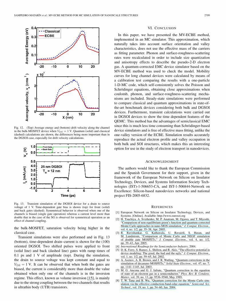
We have already commented that the MV-ECBE model canbe used in a wide variety of semiconductor devices. Fig. 11shows the electrostatic potential (top) and electron concen-tration contour plot (bottom) of the (100) bulk-nMOSFETpresented in Section IV when VG = VDS = 1 V. In Fig. 12,classical and quantum-corrected calculations are presentedfor average energy (top) and drift velocity (bottom). Ascan be observed, differences between classical and quantum(Fig. 9) velocity and energy profiles are more significant for
SAMPEDRO-MATARÍN et al.: MV-ECBE METHOD FOR MC SIMULATION OF NANOSCALE STRUCTURES 2709
Fig. 12. (Top) Average energy and (bottom) drift velocity along the channelin the bulk-MOSFET device when VDS = 1 V. Quantum (solid) and classical(dashed) calculations are shown, the differences being more important than inthe DGSOI case, especially for drift velocity calculations.
Fig. 13. Transient simulation of the DGSOI device for a drain to sourcevoltage of 1 V. Time-dependent gate bias is shown (top) for front (solid)and back gates (dashed). Symmetrical behavior is observed when one of thechannels is biased (single gate operation) whereas a current level more thandouble that in the case of the SG is observed for symmetrical operation as aneffect of channel coupling.
the bulk-MOSFET, saturation velocity being higher in theclassical case.
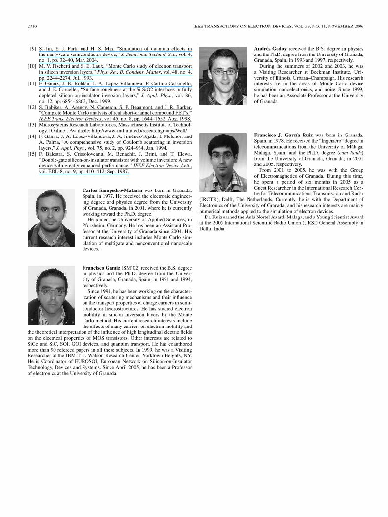
Transient simulations were also performed and in Fig. 13(bottom), time-dependent drain–current is shown for the (100)oriented DGSOI. Two shifted pulses were applied to front(solid line) and back (dashed line) gates with ramp times of0.1 ps and 1 V of amplitude (top). During the simulation,the drain to source voltage was kept constant and equal toVDS = 1 V. It can be observed that when both the gates arebiased, the current is considerably more than double the valueobtained when only one of the channels is in the inversionregime. This effect, known as volume inversion [15], is mainlydue to the strong coupling between the two channels that resultsin ultrathin body (UTB) transistors.
VI. CONCLUSION
In this paper, we have presented the MV-ECBE method,implemented in an MC simulator. This approximation, whichnaturally takes into account surface orientation and valleycharacteristics, does not use the effective mass of the carriersas fitting parameter. Phonon and surface-roughness-scatteringrates were recalculated in order to include size quantizationand anisotropy effects to describe the pseudo-2-D electrongas. A quantum-corrected EMC device simulator based on theMV-ECBE method was used to check the model. Mobilitycurves for long channel devices were calculated by means ofa calibration test comparing the results with a one-particle1-D-MC code, which self-consistently solves the Poisson andSchrödinger equations, obtaining close approximations whencoulomb, phonon, and surface-roughness-scattering mecha-nisms are included. Steady-state simulations were performedto compare classical and quantum approximations in state-of-the-art benchmark devices considering both bulk and DGSOIdevices. Furthermore, transient calculations were carried outin DGSOI devices to show the time dependent features of theQEMC. This method has the advantages of semiclassical EMCsince this is much less time consuming than Schrödinger-baseddevice simulators and is free of effective mass fitting, unlike theone-valley version of the ECBE. Simulation results accuratelyreproduce the actual electron profile and valley occupation inboth bulk and SOI structures, which makes this an interestingoption for use in the study of electron transport in nanodevices.
ACKNOWLEDGMENT
The authors would like to thank the European Commissionand the Spanish Government for their support, given in theframework of the European Network on Silicon on InsulatorTechnology, Devices, and Systems Information Society Tech-nologies (IST)-1-506653-CA, and IST-1-506844-Network onExcellence: Silicon-based nanodevices networks and nationalproject FIS-2005-6832.
REFERENCES
[1] European Network on Silicon on Insulator Technology, Devices, andSystems. [Online]. Available: http://www.eurosoi.org
[2] H. Tsuchiya, A. Svizhenko, M. P. Anatram, M. Ogawa, and T. Miyoshi,“Comparison of non-equilibrium green’s function and quantum-correctedMonte Carlo approaches in nano-MOS simulation,” J. Comput. Electron.,vol. 4, no. 1/2, pp. 35–38, Apr. 2005.
[3] R. Ravishankar, G. Kathawala, U. Ravaioli, S. Hasan, andM. Lundstrom, “Comparison of Monte Carlo and NEGF simulationof double gate MOSFETs,” J. Comput. Electron., vol. 4, no. 1/2,pp. 39–43, Apr. 2005.
[4] International Roadmap for the Semiconductor Industry, 2004.[5] D. K. Ferry, S. Ramey, L. Shifren, and R. Akis, “The effective potential in
device modeling: The good, the bad and the ugly,” J. Comput. Electron.,vol. 1, no. 1/2, pp. 59–65, Jul. 2002.
[6] A. Asenov, A. R. Brown, and J. R. Watling, “Quantum corrections in thesimulation of decanano MOSFETs,” Solid State Electron., vol. 47, no. 7,pp. 1141–1145, Jul. 2003.
[7] M. G. Ancona and G. J. Iafrate, “Quantum correction to the equationof state of an electron gas in a semiconductor,” Phys. Rev. B, Condens.Matter, vol. 39, no. 13, pp. 9536–9540, May 1989.
[8] T. W. Tang and B. Wu, “Quantum correction for the Monte Carlo sim-ulation via the effective conduction-band-edge equation,” Semicond. Sci.Technol., vol. 19, no. 1, pp. 54–60, Jan. 2004.
2710 IEEE TRANSACTIONS ON ELECTRON DEVICES, VOL. 53, NO. 11, NOVEMBER 2006
[9] S. Jin, Y. J. Park, and H. S. Min, “Simulation of quantum effects inthe nano-scale semiconductor device,” J. Semicond. Technol. Sci., vol. 4,no. 1, pp. 32–40, Mar. 2004.
[10] M. V. Fischetti and S. E. Laux, “Monte Carlo study of electron transportin silicon inversion layers,” Phys. Rev. B, Condens. Matter, vol. 48, no. 4,pp. 2244–2274, Jul. 1993.
[11] F. Gámiz, J. B. Roldán, J. A. López-Villanueva, P. Cartujo-Cassinello,and J. E. Carceller, “Surface roughness at the Si-SiO2 interfaces in fullydepleted silicon-on-insulator inversion layers,” J. Appl. Phys., vol. 86,no. 12, pp. 6854–6863, Dec. 1999.
[12] S. Babiker, A. Asenov, N. Cameron, S. P. Beaumont, and J. R. Barker,“Complete Monte Carlo analysis of real short-channel compound FET’s,”IEEE Trans. Electron Devices, vol. 45, no. 8, pp. 1644–1652, Aug. 1998.
[13] Microsystems Research Laboratories, Massachusetts Institute of Technol-ogy. [Online]. Available: http://www-mtl.mit.edu/researchgroups/Well/
[14] F. Gámiz, J. A. López-Villanueva, J. A. Jiménez-Tejada, I. Melchor, andA. Palma, “A comprehensive study of Coulomb scattering in inversionlayers,” J. Appl. Phys., vol. 75, no. 2, pp. 924–934, Jan. 1994.
[15] F. Balestra, S. Cristoloveanu, M. Benachir, J. Brini, and T. Elewa,“Double-gate silicon-on-insulator transistor with volume inversion: A newdevice with greatly enhanced performance,” IEEE Electron Device Lett.,vol. EDL-8, no. 9, pp. 410–412, Sep. 1987.
Carlos Sampedro-Matarín was born in Granada,Spain, in 1977. He received the electronic engineer-ing degree and physics degree from the Universityof Granada, Granada, in 2001, where he is currentlyworking toward the Ph.D. degree.
He joined the University of Applied Sciences, inPforzheim, Germany. He has been an Assistant Pro-fessor at the University of Granada since 2004. Hiscurrent research interest includes Monte Carlo sim-ulation of multigate and nonconventional nanoscaledevices.
Francisco Gámiz (SM’02) received the B.S. degreein physics and the Ph.D. degree from the Univer-sity of Granada, Granada, Spain, in 1991 and 1994,respectively.
Since 1991, he has been working on the character-ization of scattering mechanisms and their influenceon the transport properties of charge carriers in semi-conductor heterostructures. He has studied electronmobility in silicon inversion layers by the MonteCarlo method. His current research interests includethe effects of many carriers on electron mobility and
the theoretical interpretation of the influence of high longitudinal electric fieldson the electrical properties of MOS transistors. Other interests are related toSiGe and SiC, SOI, GOI devices, and quantum transport. He has coauthoredmore than 90 refereed papers in all these subjects. In 1999, he was a VisitingResearcher at the IBM T. J. Watson Research Center, Yorktown Heights, NY.He is Coordinator of EUROSOI, European Network on Silicon-on-InsulatorTechnology, Devices and Systems. Since April 2005, he has been a Professorof electronics at the University of Granada.
Andrés Godoy received the B.S. degree in physicsand the Ph.D. degree from the University of Granada,Granada, Spain, in 1993 and 1997, respectively.
During the summers of 2002 and 2003, he wasa Visiting Researcher at Beckman Institute, Uni-versity of Illinois, Urbana–Champaign. His researchinterests are in the areas of Monte Carlo devicesimulation, nanoelectronics, and noise. Since 1999,he has been an Associate Professor at the Universityof Granada.
Francisco J. García Ruiz was born in Granada,Spain, in 1978. He received the “Ingeniero” degree intelecommunications from the University of Málaga,Málaga, Spain, and the Ph.D. degree (cum laude)from the University of Granada, Granada, in 2001and 2005, respectively.
From 2001 to 2005, he was with the Groupof Electromagnetics of Granada. During this time,he spent a period of six months in 2005 as aGuest Researcher in the International Research Cen-tre for Telecommunications-Transmission and Radar
(IRCTR), Delft, The Netherlands. Currently, he is with the Department ofElectronics of the University of Granada, and his research interests are mainlynumerical methods applied to the simulation of electron devices.
Dr. Ruiz earned the Aula Nortel Award, Málaga, and a Young Scientist Awardat the 2005 International Scientific Radio Union (URSI) General Assembly inDelhi, India.