The LHC1 pixel detector studied in a 120GeV/c pion test beam
11
* Corresponding author. Tel.: #41-22-76-73788; fax.: #41-22-76-73394. E-mail address: iztok.ropotar@cern.ch (I. Ropotar) Nuclear Instruments and Methods in Physics Research A 439 (2000) 536}546 The LHC1 pixel detector studied in a 120 GeV/c pion test beam I. Ropotar!,",*, E.-J. Buis#, F. Antinori$, D. Barberis%, K.H. Becks", H. Beker!, P. Burger&, M. Campbell!, E. Cantatore!, L. Casagrande’, M.G. Catanesi), E. Chesi!, F. Corsi), S. D'Auria*, C. Da Via+, V. Danielyan,, G. Darbo%, D. Di Bari), S. Di Liberto-, B. van Eijk#, J. Elberich", G. Gagliardi %, R. Geppert., S. Gowdy/, C. Go K ssling0, E. Grigoriev1, T. Gys!, E.H.M. Heijne!, A.S. Howard2, G. Humpston3, J. Jakubek4, P. Jarron!, R. Leitner4, V. Lenti), M. Letheren!, B. Lisowski0, D. Loukas5, J. Ludwig., P. Martinengo!, A. Mazzoni-, F. Meddi-, P. Middelkamp!, B. Mikulec!, M. Morando$, P. Morettini%, V. O'Shea/, E. Pernigotti 6, S. Pospisil4, E. Quercigh!, N. Redaelli7, J. Ridky4, L. Rossi%, S. Saladino!,), J.C. Santiard!, L. Scharfetter!, G. Segato$, R. Shahoian,, S. Simone), K.M. Smith/, W. Snoeys!, P. Sonderegger!, B. Sopko4, I. Stekl4, L. Tomasek4, H. Vardanyan,, V. Vrba4 !CERN/EP Division, CERN Meyrin, 1211 Geneve 23, Switzerland "BUGH Wuppertal, Germany #NIKHEF Amsterdam, The Netherlands $INFN and University Padova, Italy %INFN and University Genova, Italy &Canberra Semiconductor, Olen, Belgium ’LIP Lisbon, Portugal )INFN and University of Bari, Italy *INFN and University Udine, Italy +Mu ( nchen University, Germany ,YerPhi Yerevan, Armenia -INFN and University Rome, Italy .Freiburg University, Germany /Glasgow University, UK 0Dortmund University, Germany 1Karlsruhe University and ITEP, Germany 2Imperial College, London, UK 3GEC-Marconi Materials Technology (Caswell), UK 4Praha Group, Czech Republic 5NCSR Demokritos Athens, Greece 6INFN and University Pisa, Italy 7INFN and University Milano, Italy 0168-9002/00/$ - see front matter ( 2000 Elsevier Science B.V. All rights reserved. PII: S 0 1 6 8 - 9 0 0 2 ( 9 9 ) 0 0 8 9 8 - 0
Transcript of The LHC1 pixel detector studied in a 120GeV/c pion test beam

*Corresponding author. Tel.: #41-22-76-73788; fax.: #41-22-76-73394.E-mail address: [email protected] (I. Ropotar)
Nuclear Instruments and Methods in Physics Research A 439 (2000) 536}546
The LHC1 pixel detector studied in a 120 GeV/c pion test beam
I. Ropotar!,",*, E.-J. Buis#, F. Antinori$, D. Barberis%, K.H. Becks", H. Beker!,P. Burger&, M. Campbell!, E. Cantatore!, L. Casagrande', M.G. Catanesi),E. Chesi!, F. Corsi), S. D'Auria*, C. Da Via+, V. Danielyan,, G. Darbo%,
D. Di Bari), S. Di Liberto-, B. van Eijk#, J. Elberich", G. Gagliardi%, R. Geppert.,S. Gowdy/, C. GoK ssling0, E. Grigoriev1, T. Gys!, E.H.M. Heijne!, A.S. Howard2,
G. Humpston3, J. Jakubek4, P. Jarron!, R. Leitner4, V. Lenti), M. Letheren!,B. Lisowski0, D. Loukas5, J. Ludwig., P. Martinengo!, A. Mazzoni-, F. Meddi-,
P. Middelkamp!, B. Mikulec!, M. Morando$, P. Morettini%, V. O'Shea/,E. Pernigotti6, S. Pospisil4, E. Quercigh!, N. Redaelli7, J. Ridky4, L. Rossi%,
S. Saladino!,), J.C. Santiard!, L. Scharfetter!, G. Segato$, R. Shahoian,, S. Simone),K.M. Smith/, W. Snoeys!, P. Sonderegger!, B. Sopko4, I. Stekl4, L. Tomasek4,
H. Vardanyan,, V. Vrba4
!CERN/EP Division, CERN Meyrin, 1211 Geneve 23, Switzerland"BUGH Wuppertal, Germany
#NIKHEF Amsterdam, The Netherlands$INFN and University Padova, Italy%INFN and University Genova, Italy
&Canberra Semiconductor, Olen, Belgium'LIP Lisbon, Portugal
)INFN and University of Bari, Italy*INFN and University Udine, Italy+Mu( nchen University, Germany
,YerPhi Yerevan, Armenia-INFN and University Rome, Italy.Freiburg University, Germany
/Glasgow University, UK0Dortmund University, Germany
1Karlsruhe University and ITEP, Germany2Imperial College, London, UK
3GEC-Marconi Materials Technology (Caswell), UK4Praha Group, Czech Republic
5NCSR Demokritos Athens, Greece6INFN and University Pisa, Italy
7INFN and University Milano, Italy
0168-9002/00/$ - see front matter ( 2000 Elsevier Science B.V. All rights reserved.PII: S 0 1 6 8 - 9 0 0 2 ( 9 9 ) 0 0 8 9 8 - 0

Fig. 1. Block diagram of the LHCl read-out electronics cell.
Abstract
Hybrid assemblies of LHC1 read-out chips and 300 lm thick silicon pixel detectors have been tested with a 120 GeV/cpion beam at the CERN SPS. The equivalent noise charge at the input of the preampli"er is &200 e~. The particledetection e$ciency is higher than 99.9%. A 30 ns wide e$ciency plateau is reached for a 60 ns wide trigger pulse appliedafter a &2 ls delay. The 50 lm]50 lm pixels yield a spatial precision of p"129.4$0.2 lm in the large pitch direction.In the other direction the precision is p"12.2$0.2 lm for single-pixel clusters and p"8.2$0.2 lm for double-pixelclusters, yielding an average of p"11.4$0.2 lm. Three di!erent detector layouts on the same pitch were character-ized. ( 2000 Elsevier Science B.V. All rights reserved.
Keywords: Pixel; Detector; Silicon; Test beam
1. Introduction
As part of the detector research and developmentprogramme for the future LHC machine at CERN,the RD-19 collaboration has developed the LHC1pixel tracking detector [1,2]. A comprehensive pro-gramme of test beam measurements to characterizethe detector was carried out prior to installationin a &1 100 000 pixel telescope in the WA97/NA57experiment [3}6]. Another heavy-ion experimentat CERN, NA50, is planning to upgrade the vertexregion with a &150 000 pixel cell telescope basedon the same chip [7].
The LHC1 hybrid pixel detector is describedalong with the di!erent detector layouts. The ex-perimental beam test set-up provided the positionand timing information of incoming particles aswell as a measure of the charge deposited. Thee$ciency is characterized, in particular with respectto detector bias, pixel threshold and trigger pulsetiming. Signal charge, impact location and clustersize are also correlated and spatial precision meas-urements are provided.
2. The LHC1 hybrid pixel detector
The LHC1 pixel read-out chip is a matrix of128]16 read-out cells of 50]500 lm2 [2] and itwas manufactured in the 1 lm SACMOS processfrom FASELEC. Fig. 1 shows the block diagram ofthe LHC1 electronics cell. It consists of a charge-sensitive preampli"er, a discriminator with adjust-
able threshold and Fast-OR output, a globallyadjustable delay with "ne-tuning capability in eachcell, coincidence logic and memory. If the depositedcharge passes the threshold, the discriminator "resand a pulse is sent through the delay line. A Fast-OR signal is also transmitted to the periphery of thechip. When the rising edge of the delay line outputcoincides with an externally applied trigger pulse(strobe), a one is stored in the data #ip-#op. Eachpixel read-out cell can be individually addressed forelectrical testing and masking. The read-out chip isconnected by solder bumps to a 300 lm thick sili-con sensor of the same geometry. Detector laddersto which six read-out chips are connected were alsofabricated and used to construct large-area de-tectors for the experiments [3}6]. A single-chipdetector covers a sensitive area of 8]6.35 mm2.The active sensor chip is a matrix of 128]16 ion-implanted diodes. At the periphery of the sensor
I. Ropotar et al. / Nuclear Instruments and Methods in Physics Research A 439 (2000) 536}546 537
VI. PIXEL DETECTORS

Fig. 2. (a) A photo of a few 50]500 lm2 C-type detector cells at the bottom of the detector chip, (b) A-type detector cells (one pixel cellconsists of "ve implants connected by a conductive line), and (c) a photo of C-brick-type detector cells.
Fig. 3. Schematic view of the RD19 test beam set-up at the SPSin the H6 beam line.
there are extra `dummya diodes which are connec-ted by thin lines to a guard-ring which is 230 lmwide. The guard-ring and the `dummya cells areconnected to ground via the read-out chip. Thisdesign ensures identical electrical conditions to theouter pixels. Two alternative pixel layouts wereimplemented: one with a conventional rectangularimplant (further called C-type, see Fig. 2a), and onewhere the detecting diodes consist of "ve 25]20 lm2 dot-like implants connected together bymeans of a metal line (further called A-type, seeFig. 2b). Device simulations on the two detectorcell geometries (not bump bonded to the read-outelectronics cell) yield a 78 fF capacitance for a C-type detector cell and 44 fF for the A-type detectorcell design [8]. A third pixel matrix layout containsthe conventional cells, but every second pixel row isshifted horizontally by half the cell dimension (seeFig. 2c). This C-brick-type detector matrix has beendesigned to improve the spatial precision in thedirection of large pixel pitch.
The LHC1 chip has been extensively character-ized [2,9]. Calibrations of fully assembled LHC1pixel detectors with radioactive sources which havewell-de"ned photon emission lines (109Cd, 241Am)yield a value of 15 fF for the test input capacitance.The nominal threshold for the full chip can beadjusted between &3000e~ and &11000e~. Be-yond this, gradually more pixels show a very highthreshold as the discriminator leaves its normaloperating condition. The equivalent noise chargeat the input is &100e~ r.m.s. for a chip withoutdetector and increases to &200e~ r.m.s. with de-
tector. No signi"cant di!erence in noise betweenA- and C-type detectors was observed on the meas-ured samples. This is not fully understood in viewof the di!erent detector capacitances.
3. Test beam set-up
Fig. 3 shows the beam test set-up. The trackingreference consists of two sets of crossed LHC1 pixeldetectors. The pixel detector under test is located inthe center of the tracking telescope and is read outby a VME system [10]. The trigger is provided bya coincidence of "ve scintillators de"ning an activearea of &1]2 mm2 (see Fig. 4). In parallel to thebinary hit information the charge deposited in thepixel detector is measured from the detector back-plane using a Gasplex monochannel ampli"er [11]and an ADC. The time di!erence between the trig-ger signal and the Fast-OR response of the chip is
538 I. Ropotar et al. / Nuclear Instruments and Methods in Physics Research A 439 (2000) 536}546
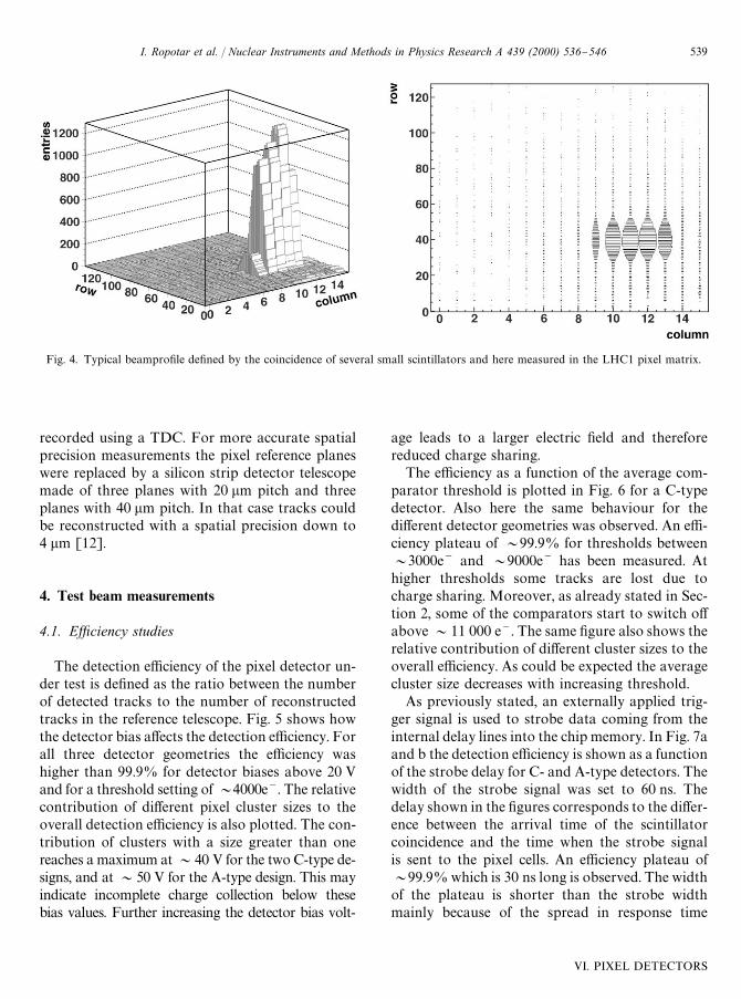
Fig. 4. Typical beampro"le de"ned by the coincidence of several small scintillators and here measured in the LHC1 pixel matrix.
recorded using a TDC. For more accurate spatialprecision measurements the pixel reference planeswere replaced by a silicon strip detector telescopemade of three planes with 20 lm pitch and threeplanes with 40 lm pitch. In that case tracks couldbe reconstructed with a spatial precision down to4 lm [12].
4. Test beam measurements
4.1. Ezciency studies
The detection e$ciency of the pixel detector un-der test is de"ned as the ratio between the numberof detected tracks to the number of reconstructedtracks in the reference telescope. Fig. 5 shows howthe detector bias a!ects the detection e$ciency. Forall three detector geometries the e$ciency washigher than 99.9% for detector biases above 20 Vand for a threshold setting of &4000e~. The relativecontribution of di!erent pixel cluster sizes to theoverall detection e$ciency is also plotted. The con-tribution of clusters with a size greater than onereaches a maximum at &40 V for the two C-type de-signs, and at &50 V for the A-type design. This mayindicate incomplete charge collection below thesebias values. Further increasing the detector bias volt-
age leads to a larger electric "eld and thereforereduced charge sharing.
The e$ciency as a function of the average com-parator threshold is plotted in Fig. 6 for a C-typedetector. Also here the same behaviour for thedi!erent detector geometries was observed. An e$-ciency plateau of &99.9% for thresholds between&3000e~ and &9000e~ has been measured. Athigher thresholds some tracks are lost due tocharge sharing. Moreover, as already stated in Sec-tion 2, some of the comparators start to switch o!above &11 000 e~. The same "gure also shows therelative contribution of di!erent cluster sizes to theoverall e$ciency. As could be expected the averagecluster size decreases with increasing threshold.
As previously stated, an externally applied trig-ger signal is used to strobe data coming from theinternal delay lines into the chip memory. In Fig. 7aand b the detection e$ciency is shown as a functionof the strobe delay for C- and A-type detectors. Thewidth of the strobe signal was set to 60 ns. Thedelay shown in the "gures corresponds to the di!er-ence between the arrival time of the scintillatorcoincidence and the time when the strobe signalis sent to the pixel cells. An e$ciency plateau of&99.9% which is 30 ns long is observed. The widthof the plateau is shorter than the strobe widthmainly because of the spread in response time
I. Ropotar et al. / Nuclear Instruments and Methods in Physics Research A 439 (2000) 536}546 539
VI. PIXEL DETECTORS

Fig. 5. E$ciency measurement as a funcion of the applied detector bias voltage: (a) for a C-type detector, (b) an A-type detector and(c) a C-brick-type detector. The threshold was set for all detectors to &4000e~.
between the observed pixel cells. The relative con-tribution of multiple cluster sizes to the overalle$ciency is plotted in both "gures. For both de-tector geometries, single-pixel events are detected"rst whereas pixel clusters of size two or bigger aredetected later. Bigger cluster sizes are due to sharedcharge, the average charge per pixel is thereforelower and detected later as the discriminator re-sponds later to signals close to threshold (time-walk). The tails in Fig. 7a and b for longer delaysare also due to timewalk. They come from events inwhich one pixel collects most of the charge and
responds in time, whilst the neighbouring pixelreceives a charge just above threshold.
Fig. 8 shows the Fast-OR response time forall clusters, single- and double-pixel clusters. TheFast-OR signals from double-pixel clusters are de-layed and have a wider distribution due to time-walk than those from single-pixel clusters. The tailsin the strobe delay measurements are not seen inFig. 8, as only the "rst Fast-OR after the scintillatorcoincidence is recorded.
It is possible to visualize the geometry of thedot-like implants in an A-type detector by selecting
540 I. Ropotar et al. / Nuclear Instruments and Methods in Physics Research A 439 (2000) 536}546

Fig. 6. Overall e$ciency as a function of the average compara-tor threshold for a C-type detector.
Fig. 7. (a) The strobe delay measurement for a C-type and (b) foran A-type detector. The threshold was set for all detectors to&4000e~.
either the early or late hits by varying the triggerlatency. Fig. 9a and b illustrate clearly that hitsnear the implants are recorded early, and furtherremoved hits are detected later. In those furtherremoved locations, incomplete charge collectiondue to a detector bias of 40 V (see also Fig. 5), en-hances the timewalk causing this e!ect to be morepronounced. In the case of the C-type detectorthe bias required for full charge collection was lowerand the e!ect was not observed.
4.2. Cluster size and charge deposition studies
Charge sharing between adjacent pixels is theprimary cause for multiple pixel clusters. It dependson the amount of charge generated, the location ofthe hit, and the detector bias and geometry. Ina binary read-out system the cluster size will alsodepend on the applied pixel threshold (see Fig. 6).Fig. 10 shows the distribution of deposited chargein ADC counts measured at the detector back sideusing a Gasplex monochannel ampli"er [11] forsingle- and double-pixel clusters. The most prob-able ADC value increases for larger pixel clustersizes as shown in Fig. 11. Fig. 12a and b showthat hits near the pixel center yield mostly single-pixel clusters, while hits near the pixel boundary
mainly lead to double-pixel clusters. Fig. 13 indi-cates that more deposited charge is required togenerate a double-pixel cluster the further the im-pact occurs from the pixel edge. In the "gure theresidual is the distance between the impact pointand the boundary between the two pixels in thecluster.
Fig. 14a compares the cluster size distribution forthe three detector geometries (A-, C- and C-brick-type) at a detector bias of 40 V and a commonthreshold setting of &4500e~. The distributionsshow a di!erence between detector types: the
I. Ropotar et al. / Nuclear Instruments and Methods in Physics Research A 439 (2000) 536}546 541
VI. PIXEL DETECTORS

Fig. 8. Fast-OR signal distribution for all clusters, single- anddouble-pixel clusters.
Fig. 9. (a) The impact points of hits which were detected `fasteraand (b) the impact points of the hits which were detected `laterain an A-type cell. For the `fastera events the island structure isclearly visible, where for the `latera events the outside of theimplants becomes visible.
A-type detector gives &5% less multiple pixel clus-ters than the C-type detectors. Increasing the de-tector bias of the A-type detector to 50 V eliminatesthe di!erence observed between the A- and theC-type (see Fig. 14b). This again points to a chargecollection loss in the A-type detector for biasesbelow 50 V, as discussed in Section 4.1.
The C-brick-type detector shows more eventsfor cluster sizes three and four as expected fromits geometry. In these cases particle hits can be re-constructed more precisely.
4.3. Spatial precision measurements
The impact point of the particles crossing thepixel detector is estimated using the reference sili-con strip telescope. The spatial precision of thistelescope was calculated as p
5%-%4#01%"40$0.2 lm
[12]. The residual is de"ned here as the lateraldistance between the reconstructed impact pointand the coordinate of the pixel cluster center. Thespatial precision of the pixel detectors, p
1*9%-is
calculated from the r.m.s. of the measured residualdistribution, p
5050!-as follows:
p21*9%-
"p2505!-
!p25%-%4#01%
.
For a binary detection system, not taking intoaccount charge sharing, the theoretical value for thespatial precision is given by the pitch of the detec-tion element l divided by J12. By this calculationone would expect the LHC1 pixel detectors withcell sizes of 50 lm]500 lm to yield a spatial pre-cision in the `columna direction of p
#0-6./"
144.3 lm and p308
"14.4 lm in the smaller `rowadirection.
542 I. Ropotar et al. / Nuclear Instruments and Methods in Physics Research A 439 (2000) 536}546

Fig. 10. Charge deposition distribution (in ADC counts) forsingle-pixel (lightly shaded) and double-pixel clusters (dark)measured at the back contact for a threshold setting of&4000e~.
Fig. 11. Charge measured on the back contact as a function ofthe pixel cluster size for a threshold setting of &4000e~.
Fig. 12. (a) The position of the impact points where one pixelresponded to a particle hit and (b) the position of the impactpoints where two adjacent pixels responded to a particle hitprojected into one-detector pixel cell (sizes not to scale). In caseswhere one pixel responds to a particle hit most of the hits arelocated in the cell center, when two pixel respond to a hit theimpact points mostly surround the pixel border. The thresholdwas set to &4000e~ during this measurement.
Figs. 15}17 show the measured residual distribu-tions for single-pixel clusters for the C- and A-typedetector geometries in the `columna and `rowadirections. The single-pixel cluster precisions werethe same for A-type and C-type pixels and cal-
culated to be
pC-5:1%, 4*/'-%-#0-6./
"pA-5:1%, 4*/'-%-#0-6./
"129.4$0.2 lmpC-5:1%, 4*/'-%-308
"pA-5:1%, 4*/'-%-308
"12.2$0.2 lm .
I. Ropotar et al. / Nuclear Instruments and Methods in Physics Research A 439 (2000) 536}546 543
VI. PIXEL DETECTORS

Fig. 13. Correlation between the residual and the most probableADC value for double-pixel clusters measured for a thresholdsetting of &4000e~.
Fig. 14. (a) The distribution of cluster sizes for an applieddetector bias of 40 V for all three di!erent detector geometriesand (b) shows the distribution of cluster sizes where the detectorbias for the C-type detectors was set to 40 and 50 V for theA-type detector.
In Figs. 18 and 19 the residual distributions fordouble-pixel clusters in the row direction areshown for a C-type and an A-type detector. Thecorresponding precisions are calculated as
pC-5:1%, $06"-%
"9.8$0.2 lm,
pA-5:1%, $06"-%
"8.2$0.2 lm .
Excluding the tail of these distributions, which re-sult from high charge deposition, a Gaussian "t tothe remaining data gives more optimistic values ofsigma indicated in the "gures. Taking into accountthe residuals for both single and double clusters theaverage spatial precision in the smaller row direc-tion is
pC-5:1%, !7%3!'%-308
"11.8$0.2 lm,
pA-5:1%, !7%3!'%-308
"11.4$0.2 lm .
As expected due to the use of the charge sharinginformation (double hits), both values are smallerthan the one predicted for a simple binary detectionsystem which does not take the charge sharing intoaccount.
Although these results show a slight resolutionimprovement for the A-type detector, a clear
conclusion can not be drawn as both detectors havebeen operated with a detector bias of 40 V at whichthe A-type detector does not show full charge col-lection e$ciency (see Fig. 14).
5. Conclusions
Three di!erent detector layouts were bumpbonded to LHC1 read-out chips and characterisedin a 120 GeV/c pion beam at the CERN SPS. Fullparticle detection e$ciency was obtained abovea detector bias of &20 V in a threshold rangebetween &3000e~ and &11 000e~. A 30 ns wide
544 I. Ropotar et al. / Nuclear Instruments and Methods in Physics Research A 439 (2000) 536}546

Fig. 15. Residual distribution for single-pixel clusters in thelarger `columna direction measured for a C-type detector.
Fig. 16. Residual distribution for single-pixel clusters in the`rowa direction for a C-type detector.
Fig. 17. Residual distribution for single-pixel clusters in the`rowa direction for an A-type detector.
Fig. 18. Residual distribution for double-pixel clusters for aC-type detector.
e$ciency plateau was measured for a 60 ns widetrigger pulse applied after a &2 ls delay. Althoughall particles were detected in time, charge sharing inthe detector coupled with the timewalk of the dis-criminator resulted in some trailing hits. Fast-ORmeasurements indicated that double-hit clusterswere on average slower than single-hit events. Thecharge measured on the back contact of the de-
tectors was correlated to the response of the pixelread-out chip. Spatial precision measurementsof the 50 lm]500 lm A- and C-type pixels yielda precision of p"129.4$0.2 lm in the large pitchdirection. In the smaller direction the precisionfor the A-type detector is p"12.2$0.2 lm forsingle-pixel clusters and p"8.2$0.2 lm fordouble-pixel clusters, yielding an average precision
I. Ropotar et al. / Nuclear Instruments and Methods in Physics Research A 439 (2000) 536}546 545
VI. PIXEL DETECTORS
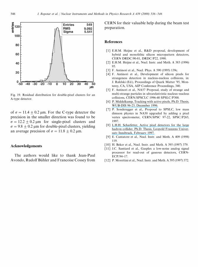
Fig. 19. Residual distribution for double-pixel clusters for anA-type detector.
of p"11.4$0.2 lm. For the C-type detector theprecision in the smaller direction was found to bep"12.2$0.2 lm for single-pixel clusters andp"9.8$0.2 lm for double-pixel clusters, yieldingan average precision of p"11.8$0.2 lm.
Acknowledgements
The authors would like to thank Jean-PaulAvondo, Rudolf BuK hler and Francoise Cossey from
CERN for their valuable help during the beam testpreparation.
References
[1] E.H.M. Heijne et al., R&D proposal, development ofhybrid and monolithic silicon micropattern detectors,CERN DRDC/90-81, DRDC/P22, 1990.
[2] E.H.M. Heijne et al., Nucl. Instr. and Meth. A 383 (1996)95.
[3] F. Antinori et al., Nucl. Phys. A 590 (1995) 139c.[4] F. Antinori et al., Development of silicon pixels for
strangeness detection in nucleus-nucleus collisions, in:J. Rafelski (Ed.), Proceedings of Quark Matter '95, Mon-terey, CA, USA, AIP Conference Proceedings, 340.
[5] F. Antinori et al., NA57 Proposal, study of strange andmulti-strange particles in ultrarelativistic nucleus}nucleuscollisions, CERN/SPSCLC 1996-40 SPSLC/P300.
[6] P. Middelkamp, Tracking with active pixels, Ph.D. Thesis,WUB-DIS 96-23, December 1996.
[7] P. Sonderegger et al., Proposal to SPSLC, low massdimuon physics in NA50 upgraded by adding a pixelvertex spectrometer, CERN/SPSC 97-22, SPSC/P265,1997.
[8] L.H.H. Scharfetter, Active pixel detectors for the largehadron collider, Ph.D. Thesis, Leopold Franzens Univer-suty Innsbruck, February 1997.
[9] E. Cantatore et al., Nucl. Instr. and Meth. A 409 (1998)119.
[10] H. Beker et al., Nucl. Instr. and Meth. A 395 (1997) 379.[11] J.C. Santiard et al., Gasplex a low-noise analog signal
processor for read-out of gaseous detectors, CERN-ECP/94}17.
[12] P. Morettini et al., Nucl. Instr. and Meth. A 395 (1997) 372.
546 I. Ropotar et al. / Nuclear Instruments and Methods in Physics Research A 439 (2000) 536}546