Control of Tensile Stress in Prestressed Concrete Members ...

www.elsevier.com/locate/actamat
Acta Materialia 55 (2007) 5201–5210
Tensile strength of gold nanointerconnects without the influenceof strain gradients
Sven Olliges a, Patric A. Gruber b, Vaida Auzelyte c, Yasin Ekinci c,Harun H. Solak c, Ralph Spolenak a,*
a Laboratory for Nanometallurgy, Department of Materials, ETH Zurich, Wolfgang-Pauli-Strasse 10, CH-8093 Zurich, Switzerlandb Universitat Stuttgart, Institut fur Metallkunde, Heisenbergstrasse 3, D-70569 Stuttgart, Germany
c Paul Scherrer Institute, Laboratory for Micro- and Nanotechnology, CH-5232 Villigen-PSI, Switzerland
Received 19 March 2007; received in revised form 28 May 2007; accepted 29 May 2007Available online 16 July 2007
Abstract
Gold is an ideal material for wires and electrodes on the nanoscale because of its corrosion resistance and biocompatibility. For sys-tem integration the mechanical properties of gold nanowires are highly important. In this paper, a study on the deformation behavior ofparallel line arrays of gold on polyimide substrates is presented. Arrays of 45–60 nm nanolines were produced by extreme ultravioletinterference lithography, evaporation of gold and a subsequent lift-off process. Tensile testing of these samples was performed by usingan in situ synchrotron-based technique, which allows for the fast acquisition of diffraction peaks. The samples show yield stresses ofabout 400 MPa. This is comparable to thin films of similar thickness, but significantly lower than previously reported results on singleelectrodeposited wires deformed in bending. The differences are explained in terms of strain gradient plasticity theory.� 2007 Acta Materialia Inc. Published by Elsevier Ltd. All rights reserved.
Keywords: Lithography; Tension test; X-ray diffraction; Nanocrystalline materials; Plastic deformation
1. Introduction
Nanostructured materials such as nanowires, nanorodsor nanotubes have attracted considerable interest in the last20 years. The development of fabrication techniques pro-viding such small dimensions as well as the developmentof modern high-resolution microscopic methods likeatomic force microscopy (AFM), scanning tunnelingmicroscopy (STM), focused ion beam (FIB) microscopyor the latest generation of scanning electron microscopes(SEM) have enabled small-scale samples to be studied.The steady increase in computing power, which hasenabled the simulation and modulation of complete nano-systems, has contributed to this development.
In earlier studies, nanolines on substrates were producedby conventional photolithography (patterning of a resist,
1359-6454/$30.00 � 2007 Acta Materialia Inc. Published by Elsevier Ltd. All
doi:10.1016/j.actamat.2007.05.039
* Corresponding author.E-mail address: [email protected] (R. Spolenak).
development and metallization by physical vapor deposi-tion (PVD) or electrochemical deposition) and subsequentthinning of the structures [1]. Narrower lines with remark-ably higher packing densities on the substrate becameavailable with the development of electron beam lithogra-phy (EBL). Line widths down to 10 nm with periodicitiesof few tens of nanometers as well as complicated shapeswere possible. The availability of higher sample quantitiesin the nanorange is associated with the development of syn-chrotron-based techniques such as ‘‘Lithographie, Galva-nik und Abformung’’ (LIGA) [2] or extreme ultravioletinterference lithography (EUV-IL) [3] as used in this paper.In addition, several chemical procedures have recentlybecome available for the production of nanoparticles andnanorods [4,5].
Most of the investigations on nanoshaped materials,however, are based on simulation techniques such asmolecular dynamics (MD) or ab initio calculations. DaSilva et al. [6] investigated the fracture behavior of atomic
rights reserved.

1 The authors feel confident that nanointerconnects on polymericsubstrate will be relevant for future applications in micro-electronicsrather than freestanding nanowires or nanorods.
5202 S. Olliges et al. / Acta Materialia 55 (2007) 5201–5210
gold nanowires under tensile load. Atomic wires werefound to deform by necking and the formation of stackingfaults. Just before fracture, the neck consisted of a singleatomic chain. Mechanical properties of gold nanowireswith a square base of 4 nm · 4 nm and 12 nm long werecalculated by an atomistic simulation method by Diaoet al. [7]. The ultimate strength for (111) oriented nano-wires was found to be 4 GPa at a fracture strain of about4%. (100) oriented nanowires with identical dimensionsshow approximately the same ultimate strength but atremarkably higher fracture strains of about 10% which isdue to the elastic anisotropy of gold. Unlike the experi-ments in tension, it was found that compressive yieldstrengths strongly depend on the orientation of the nano-wires: about 4 GPa for the (111) orientation and only afew hundreds of MPa for the (100) orientation. The frac-ture behavior of 7–1 gold shells was simulated (usingMD) by Ju et al. [8], and ultimate strengths at room tem-perature (RT) of up to 3 GPa at fracture strains of 6% wereobtained. A further interesting effect was observed by Diaoet al. [9]. Surface tension induces a phase transformation ofwires with a square base, where the face-centered cubic(fcc) lattice transforms into a body centered tetragonal(bct) 1 or bct2 lattice depending on the initial base length(in the range of 1.83–30 nm). The general effect of phasetransformation under compressive stresses could be verifiedby static simulation of bulk gold under compression.
Experimental evidence for the theoretical predictions israre since the fabrication of nanoshaped materials as wellas experiments in the nanoregime still poses a great chal-lenge. Nevertheless, several techniques have been success-fully applied for testing materials in the nanorange, e.g.(i) X-ray techniques for the investigation of microlinesand thin films; (ii) nanoindentation for analyzing micro-and nanopillars; and (iii) combinations of several micro-scopic techniques, such as an AFM/STM in a SEM or anAFM in combination with a STM for investigating nano-wires, nanocontacts and nanotubes.
The first experiments on thermal stress relaxation incopper microlines on silicon substrate were performed byBesser et al. [10] using the sin2(w) technique, which isdescribed in detail in Noyan et al. [11]. The same techniquewas applied for the investigation of thermal stress relaxa-tion in passivated Al–0.5% Cu microlines by Greenebaumet al. [12]. The local stress distributions in unpassivatedAl–0.5% Cu microlines and thin films were measured bySpolenak et al. [13] using micro-diffraction. A novel X-ray in situ technique was developed by Bohm et al. [14]for tensile testing of metal thin films on a flexible polymersubstrate with thicknesses of down to 10 nm. Yield stressesof about 600 MPa for gold thin films with thicknesses of80–1000 nm and decreased yield stresses of about400 MPa for gold thin films with thicknesses in the rangeof 20–60 nm were observed [14,15]. Considerably higheryield stresses were obtained by uniaxial compression testingof single crystal (SC) micropillars using nanoindentation.Greer et al. [16,17] and Volkert et al. [18] report yield stres-
ses for SC gold pillars obtained by FIB preparations of aSC gold film of 550 MPa for pillar diameters of 400 nm[16], and 1 GPa for pillar diameters of 300 nm [18]. Exper-iments on nanonecks in the regime of few nanometers wereperformed by Agrait et al. [19], Stalder et al. [20] andMarszalek et al. [21]. The necks are formed by indentinga gold-coated AFM (or STM) tip into a gold substrateand retracting the tip. The high force resolution of theAFM and an estimation of the contact area (e.g. by theeffective spring constant [19]) allow the calculation of flowstresses. Yield stresses for the nanonecks were in the rangeof 1–5 GPa. If the size of the necks was reduced to the sizeof an atomic chain (diameter of the neck <1 nm), yieldstresses of about 12–15 GPa were calculated by Rubioet al. [22] and Rubio-Bollinger et al. [23] using the sametechnique. This is consistent with simulations of 0.7 nmgold multishells by Gall et al. [24] which reach a yield stressof about 13 GPa. Bending experiments on polycrystallinenanowires were performed by Wu et al. [25]. The nanowireshad diameters in the range of 40–250 nm and were pro-duced electrochemically in nanoporous alumina. The wireswere tested by pinning them over trenches and subsequentbending by an AFM. Yield stresses of about 3.5 and5.6 GPa were observed for wires with diameters of 200and 40 nm, respectively.
In this paper, an in situ tensile testing study on techni-cally relevant1 gold nanointerconnects is presented. Theauthors apply the in situ technique developed by Bohmet al. [14] to parallel line arrays of gold on polyimide sub-strate. The arrays consist of 5000 lines which have lengthsof 1 mm, widths of 45–60 nm, heights of 20–30 nm andperiodicities of 100 nm. This technique provides statisti-cally relevant results since (i) the lattice strain of each exter-nal load level is acquired independently of the deformationhistory and (ii) integrated information of an ensemble of5000 identical nanolines is obtained.
2. Experimental
The nanowires were fabricated using EUV-IL [3] and alift-off process. The periodic line pattern was exposed atthe XIL beamline of the Swiss Light Source (SLS) [26].The pattern consists of 1 mm long parallel 100 nm periodlines covering an area of 0.5 mm2. The exposure was car-ried out on a 125 lm thick polyimide substrate (Kapton�HN film, Du Pont) with low surface roughness. Two resistlayers were used to ensure a successful lift-off process. Abilayer of 50 nm PMMA (polymethylmethacrylat) and30 nm HSQ (hydrogen silsesquioxane) was spin-coatedonto the Kapton� film. First, the line pattern was exposedin the negative tone HSQ resist layer that was developedin 25% TMAH (tetra-methyl-ammonium hydroxide) solu-tion for 15 s. In the next step, the HSQ pattern was used

S. Olliges et al. / Acta Materialia 55 (2007) 5201–5210 5203
as a hard mask for dry etching of the underlying PMMAfilm in oxygen plasma. This process leads to a profile witha significant undercut, which is needed for the followinglift-off step. Lift-off in acetone was performed after thethermal evaporation of 20–30 nm gold. Prior to the golddeposition, 4 nm of chromium were deposited on Kap-ton� to improve the adhesion of gold lines to the sub-strate. We observed that when the surface of the
Fig. 1. Representative SEM micrograph (a) before and (b) after tensile testinglength of 1 mm, widths of 40–60 nm, heights of 20–30 nm and periodicity of 100distances of 1–2 lm are visible (b).
Kapton� film was exposed to oxygen plasma during thePMMA etch step, the deposited Cr/Au film was roughand had a grainy texture. This problem was solved by cov-ering the Kapton� film with several nanometers of chro-mium prior to resist coating. In this way 25–60 nm widelines with a periodicity of 100 nm were produced. ASEM image of 58 nm wide lines is shown in Fig. 1 as anexample. The length of the samples was extended by addi-
(both pictures are taken from sample B). In general, the lines have uniformnm. After tensile testing, delamination lines perpendicular to the lines with

36 37 38 39 40 41 42 43 44 4540000
50000
60000
70000
80000
90000
100000
Inte
nsity
35 36 37 38 39 40 41 42 4360000
70000
80000
90000
100000
Inte
nsity
2θ 2θ
a b c
(111) Au
(110) W
strain markers
area of nanointerconnectsadditional Kapton
(111) Au
(110) W
Fig. 2. Illustration of the raw data: (a) strain measurement, (b) detector signal in transverse direction, (c) detector signal in load direction. Even though thediffracting volume is very small, the gold peaks are well resolved by the microstrip detectors. The oblique underground in load directions is due to the focusof the synchrotron beam.
5204 S. Olliges et al. / Acta Materialia 55 (2007) 5201–5210
tional Kapton� segments by a gluing process to adapt thesample length to the tensile tester applied and to avoidshadowing of the X-rays.
The line arrays were tested at the Materials Science(MS) Beamline at the SLS by an in situ technique, whichwas originally developed for tensile testing of metal thinfilms by Bohm et al. [14]. This technique measures thechanges in lattice strain as a function of external loadand is described in detail in Ref. [14]. Sample load is gener-ally associated with changes in lattice strains, which areobserved by X-ray diffraction. The energy of the X-raybeam has to be adjusted to the sample texture in order toobtain a Debye–Scherrer ring for normal beam incidence.Due to sample symmetry it is convenient to observe thechanges in lattice strain for the principal axis of theDebye–Scherrer ring which correspond to the load eL(N)and the transverse eT(N) direction, where N is an integernumber and indicates the external load level applied bythe tensile tester to the sample. The detector signal forthe principal axes of the Debye–Scherrer ring is shown inFig. 2b and c. The lattice strain is calculated in terms ofprincipal strains e1(N), e2(N) and subsequently convertedinto principal stresses r1(N), r2(N) by Hooke’s Law. It isimportant to note that e3(N) depends linearly on e1(N)and e2(N) due to the boundary condition r3 = 0 for unpass-ivated samples. External strains e are measured by trackingtwo markers close to the parallel line ensemble using aLaVision photographic system (Fig. 2a). At least onemicrograph is taken for each external load level N. Dataare analyzed using a MatLab routine developed by Eberlet al. [27]. This allows for a ‘‘local’’ determination of thestrain e(N) as a function of the external load level N.
Finally, the experimental data of strain e(N) and stressesr1(N), r2(N) are merged to give ‘‘full’’ stress–strain curves
r1 (e) and r2 (e). It is important to consider that this tech-nique measures relative stresses and not absolute stresses.This technique can be transferred fully from thin films toour parallel line arrays. The only important requirementis an unpassivated, free surface of the samples in order tosatisfy the assumption r3 = 0 (cf. [14]), which is the casein our experiment. Since the parallel nanoline arrays showthe same (111) texture as the thin films of Bohm et al. [14](cf. inset of Fig. 8), the explicit formalism for (111) tex-tured samples can be used without any modification.
3. Methods
The tensile tester (Kammrath & Weiss) was mounted onthe x/y// powder diffractometer of the MS beamline [28](Fig. 3). Using a left-handed Cartesian coordinate system,the X-ray beam is in the x-direction, the load axis is in thez-direction and the parallel line array is in the y/z plane(where the nanointerconnects are aligned in the z-direc-tion). The X-ray beam was adjusted to the (111) textureof the gold lines and had an energy of 7.97 keV. Two sec-ond-generation microstrip detectors (line detectors)[29,30] are mounted in the x/z plane (load direction) andin the x/y plane (transverse direction) for monitoringchanges in the lattice strain. The distance and position ofthe detectors are chosen to observe diffraction angles ofabout 38 ± 4�, corresponding to the diffraction angle ofthe [111] peak of gold for the X-ray energy used (cf.Fig. 2b and c).
A thin film of tungsten powder suspended in vacuumgrease is applied to the reverse side of the Kapton� sub-strate. The positions of the tungsten peak and theunstressed gold peak (image number N = 1) are assignedto their corresponding 2h angles in order to calibrate the
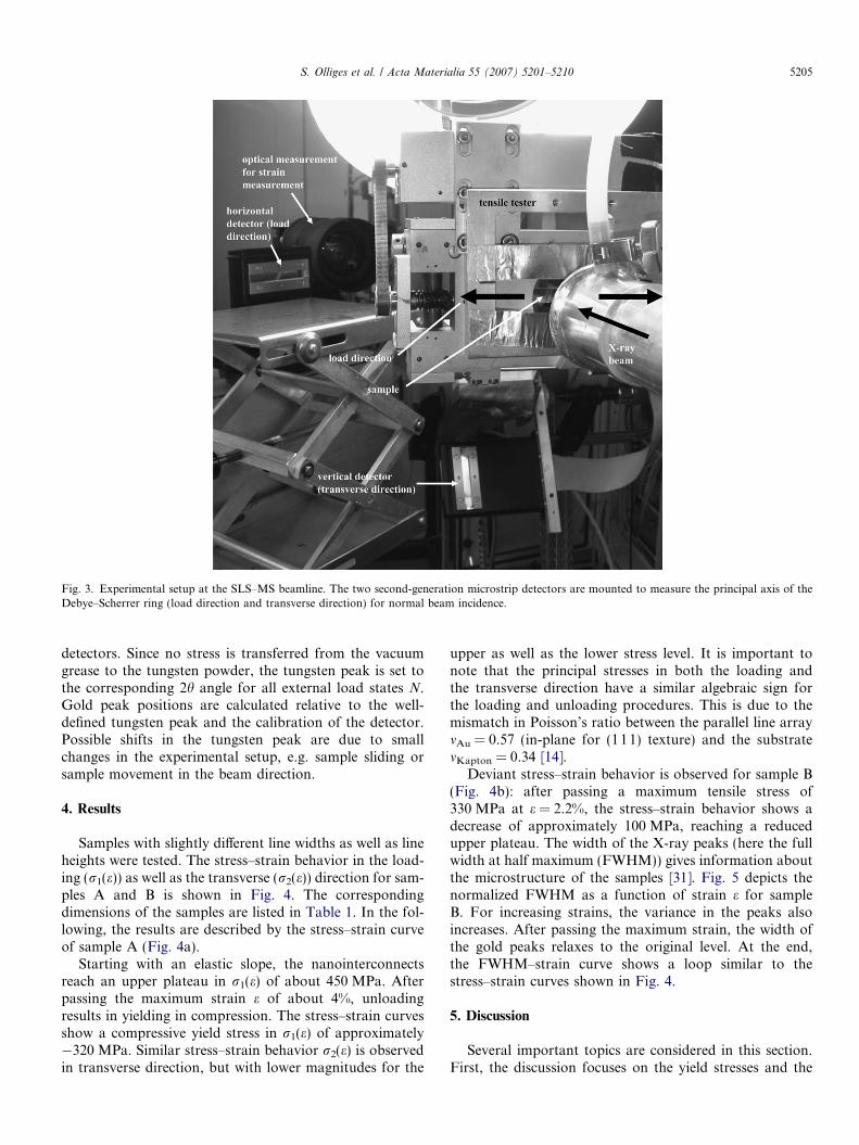
Fig. 3. Experimental setup at the SLS–MS beamline. The two second-generation microstrip detectors are mounted to measure the principal axis of theDebye–Scherrer ring (load direction and transverse direction) for normal beam incidence.
S. Olliges et al. / Acta Materialia 55 (2007) 5201–5210 5205
detectors. Since no stress is transferred from the vacuumgrease to the tungsten powder, the tungsten peak is set tothe corresponding 2h angle for all external load states N.Gold peak positions are calculated relative to the well-defined tungsten peak and the calibration of the detector.Possible shifts in the tungsten peak are due to smallchanges in the experimental setup, e.g. sample sliding orsample movement in the beam direction.
4. Results
Samples with slightly different line widths as well as lineheights were tested. The stress–strain behavior in the load-ing (r1(e)) as well as the transverse (r2(e)) direction for sam-ples A and B is shown in Fig. 4. The correspondingdimensions of the samples are listed in Table 1. In the fol-lowing, the results are described by the stress–strain curveof sample A (Fig. 4a).
Starting with an elastic slope, the nanointerconnectsreach an upper plateau in r1(e) of about 450 MPa. Afterpassing the maximum strain e of about 4%, unloadingresults in yielding in compression. The stress–strain curvesshow a compressive yield stress in r1(e) of approximately�320 MPa. Similar stress–strain behavior r2(e) is observedin transverse direction, but with lower magnitudes for the
upper as well as the lower stress level. It is important tonote that the principal stresses in both the loading andthe transverse direction have a similar algebraic sign forthe loading and unloading procedures. This is due to themismatch in Poisson’s ratio between the parallel line arraymAu = 0.57 (in-plane for (11 1) texture) and the substratemKapton = 0.34 [14].
Deviant stress–strain behavior is observed for sample B(Fig. 4b): after passing a maximum tensile stress of330 MPa at e = 2.2%, the stress–strain behavior shows adecrease of approximately 100 MPa, reaching a reducedupper plateau. The width of the X-ray peaks (here the fullwidth at half maximum (FWHM)) gives information aboutthe microstructure of the samples [31]. Fig. 5 depicts thenormalized FWHM as a function of strain e for sampleB. For increasing strains, the variance in the peaks alsoincreases. After passing the maximum strain, the width ofthe gold peaks relaxes to the original level. At the end,the FWHM–strain curve shows a loop similar to thestress–strain curves shown in Fig. 4.
5. Discussion
Several important topics are considered in this section.First, the discussion focuses on the yield stresses and the

-1 0 1 2 3 4 5 6 70.90
0.92
0.94
0.96
0.98
1.00
1.02
1.04
1.06
1.08
1.10
1.12
1.14ω
1 sample B (30 nm)
ω1 [c
hann
els]
Strain [%]
Fig. 5. FWHM in load direction of the gold peaks as a function of theapplied strain e of sample B. The FWHM is normalized by the FWHM ofthe first image (N = 1). For clarity, the original data are smoothed by athree-point fast Fourier transformation (line).
0 1 2 3 4 5 6 7
7
-500
-400
-300
-200
-100
0
100
200
300
400
500
600σ1 A (20 nm)σ2 A (20 nm)
σ [M
Pa]
ε [%]
0 1 2 3 4 5 6-500
-400
-300
-200
-100
0
100
200
300
400
500
600σ1 B (30 nm)σ2 B (30 nm)
Δσ
[MPa
]
ε [%]
a
b
Fig. 4. Representative stress–strain behavior of parallel line arrays of goldfor (a) sample A and (b) sample B. The properties of the line arrays arelisted in Table 1. For clarity, the original data are smoothed by a three-point fast Fourier transformation (line).
5206 S. Olliges et al. / Acta Materialia 55 (2007) 5201–5210
residual stress. Next, cracking and delamination of thenanolines are analyzed according to a theory of Xia andHutchinson [32] that considers the transfer of strain fromflexible substrates to the line arrays. Finally, the yield stres-ses of the nanointerconnects are compared with the yieldstresses of thin films obtained by tensile testing [15] as well
Table 1Overview of the samples: the arrays show uniform length of 1 mm. The averagean oscillating crystal in the deposition system. For better adhesion of the gold
Sample Average line width (nm) Line height (nm)
A 47 ± 2 20 ± 2B 58 ± 2 30 ± 2C 59 ± 2 20 ± 2D 44 ± 2 20 ± 2E 60 ± 2 18 ± 2
The yield stresses are obtained by an intersection of r(e) and the elastic slope atstresses are listed.
as with the yield stresses of nanowires obtained by bendingexperiments [25]. The latter requires the introduction ofstrain gradient plasticity theory.
The measurement of residual stresses rr at the synchro-tron was not possible due to time constraints and becausethe goniometer lacked all the required degrees of freedom.As the residual stress rr is an important quantity, threestrategies were used to determine it: the postulation of asymmetric yield behavior in tension and compression, mea-surements of residual stresses on blanket films deposited inthe proximity of the nanowires, and an estimation of resid-ual stress from the deposition conditions.
In general, these samples show plateaux at ryt (tensilestress) and at ryc (compressive stress), where jrycj 6¼ jrytj(Fig. 4a). The FWHM of the X-ray peaks as a functionof strain (Fig. 5) indicates that no dislocation networksare formed, which excludes a Bauschinger effect as anexplanation for the non-equality of jrycj and jrytj. Conse-quently, the difference in absolute value of ryt and ryc
has to be caused by another asymmetric effect, which isassumed to be the residual stress rr. To obtain the expectedplateaux at ±ry, the stress–strain curves have to be shiftedby
widths are obtained by SEM micrographs and the heights are obtained bylines to the substrate, 4 nm of Cr are deposited before gold deposition
Yield stress (MPa) Corrected yield stress (MPa)
450 385330 265430 365400 335470 405
e = 0.5%. In the last column, the residual stress of �65 MPa corrected yield

S. Olliges et al. / Acta Materialia 55 (2007) 5201–5210 5207
� ryt þ ryc
2:¼ rr: ð1Þ
For ryt = 450 MPa and ryc � �320 MPa (sample A), aresidual stress of rr = �65 MPa is calculated from Eq. (1).
This estimation assumes that the residual stress is theonly asymmetric effect in the nanolines. To strengthen thisassumption we present some additional arguments whichconfirm the value of residual stress obtained by Eq. (1).
First, the residual stress rr is measured by sin2(w) exper-iments [11] using common X-ray diffraction (XRD) systems(Eulerian cradle and monocapillary with 300 lm spot size).The residual stress is measured on homogeneous pads pres-ent on the same Kapton� wafer that are identical to thenanowires in terms of deposition history as well as micro-structure. The XRD configuration for measuring the resid-ual stress using the (111) peaks, which have to be usedbecause of the small scattering volume of the sample, isvery sensitive to small misalignments in sample height. Acalibration substance (BaO2 powder suspended in vacuumgrease) is applied on the top of the samples to minimize thisundesirable effect. Two different XRD lab systems are usedto avoid systematic alignment errors. However, all mea-surements yield results in the range of �40 to �110 MPa,which is in good agreement with the residual stress rr of�65 MPa obtained from Eq. (1).
The residual stress can be verified by another estimationusing the differences in thermal expansion of the polyimidesubstrate and the gold line arrays. The effective stiffness(Young’s modulus · thickness) of polyimide exceeds thestiffness of a reference homogeneous 30 nm gold thin film(corresponding to the maximum height of the line arrays)by two orders of magnitude. Consequently, the strain ofthe line arrays is given by the substrate. Accordingly, theresidual stress is given by
rr � ðaKapton � aAuÞ � EAu � DT ; ð2Þwhere aKapton and aAu are the thermal expansion coeffi-cients of polyimide and gold, respectively, DT = T0 � Td
is the temperature difference between room temperatureT0 and deposition temperature Td, and EAu is the Young’smodulus of gold. For aKapton = 30 · 10�6 K�1 2,aAu = 14.2 · 10�6 K�1, EAu = 80 GPa (corresponding tothe (11 0) in-plane isotropy for (111) textured samples)and the above estimated residual stress of rr = �65 MPa,an increased temperature for gold deposition of about50 K with respect to room temperature is obtained, whichis reasonable.
The exclusion of a Bauschinger effect may be contrary tothe observations of Xiang and Vlassak [33,34]. However,the formalism described by Xiang and Vlassak [34] is basedon the interaction of numerous dislocations per grainwhich are indeed present in their thin films in the thicknessrange of several hundreds of nanometers (sub-micron
2 Thermal expansion of Kapton� is in the range 30–60 · 10�6 K�1.From experience, the Kapton� foils tend to the lower value of30 · 10�6 K�1, and this value is used for further calculations.
range) to several microns. In comparison, the thicknessas well as the average grain size of the parallel line arraysin the current study is at least one order of magnitude smal-ler. Consequently, less than one dislocation per grain is onaverage expected for the nanointerconnects, if a similar dis-location density is assumed. Hence, no dislocation net-works are expected to form at the sample/substrateinterface, which is commonly quoted as the origin of theBauschinger effect in thicker films [34].
The yield stresses ry are obtained by the intersection of aline parallel to the elastic slope at e = 0.5% and r1(e). Forexample, samples A and B show yield stresses of 450 and330 MPa, respectively. As a consequence of residual stress,the stress–strain behavior shown in Fig. 4 has to be cor-rected by the above estimated residual stress rr of�65 MPa, resulting in ‘real’ yield stresses of 385 and265 MPa, respectively (compare Table 1).
Strain transfer from substrates to thin films is discussedin detail by Xia and Hutchinson [32]. They report charac-teristic length scales l for transferring stresses from sub-strates to thin films depending on Dundur’s parameters aand b [35] defined by
a ¼ E1 � E2
E1 þ E2
; and b ¼ l1ð1� 2m2Þ � l2ð1� 2m1Þ2l1ð1� m2Þ þ 2l2ð1� m1Þ
; ð3Þ
where Ei ¼ Ei=ð1� m2i Þ are the plane strain tensile moduli,
li are the shear moduli, Ei are Young’s moduli and mi arethe Poisson’s ratios of the sample (i = 1) and the substrate(i = 2). These parameters account for the mismatch in elas-tic properties between substrate and sample materials. Thelength scale l for full stress transfer is given by [32]
l ¼ p2
gða; bÞ � h; ð4Þ
where g(a,b) is a function described by Beuth [36] and h isthe film thickness. Since g(a,b) depends strongly on a andonly weakly on b, we neglect the weak dependence on b forfurther considerations. For EAu = 80 GPa, mAu = 0.57(in-plane for (111) texture), EKapton = 3 GPa andmKapton = 0.34, a Dundur’s parameter of a = 0.94 isobtained, corresponding to g(a,b) � 10 and a characteristiclength scale l of approximately 15h [32]. For sample heightsh of 20–30 nm, a characteristic length l for full strain trans-fer (from Kapton� to the parallel line array of gold) of lessthan 500 nm is expected. Since the length of the line arrays(1 mm) exceeds this value by three orders of magnitude,this fringe effect should be negligible for ductile materialssuch as gold.
Nevertheless, if samples show stress relaxation (tensileas well as compressive stress relaxation), e.g. due to pooradhesion of the lines to the substrate, the lines are expectedto crack at points of maximum strain. Thus, crack dis-tances in the range of 2l are expected. This is consistentto the observations of Gruber et al. [37] for Ta/Cu/Ta mul-tilayer thin films. Sample A (Fig. 4a) does not show obvi-ous evidence of delamination. In contrast, sample B(Fig. 4b) shows a clear decrease of about 100 MPa after

5208 S. Olliges et al. / Acta Materialia 55 (2007) 5201–5210
passing the maximum stress at strains of 1.5–2%, indicatingtensile stress relaxation due to line cracking or delamina-tion of the lines [14]. The delamination of the lines is mostprobably caused by an insufficient adhesion of the lines.This can be confirmed by post-testing SEM micrographs,which show delamination/buckling lines perpendicular tothe nanointerconnects (Fig. 1b). The distances of thesedelamination/buckling lines are in the range of 1–2 lm,which is in good agreement to the distance of 2l � 1 lmestimated above. Since it is assumed that the early delami-nation of sample B at strains of about 1.5–2% influencesthe yield stress, this sample shows rather a ‘‘delaminationthreshold stress’’ than a typical yield stress (which isremarkably lower in comparison to the yield stress of sam-ple A).
The ‘‘real’’ stress–strain behaviors of the nanointercon-nects are compared to the behaviors of gold thin filmsobtained by the same tensile technique [15]. The nanointer-connects show, in a good agreement, the same stress–strainbehavior as the homogeneous gold thin films of equalthickness (Fig. 6). From this we conclude that nanolinesand thin films have comparable grain sizes, which areassumed to be the governing strengthening mechanism [15].
On the other hand, the obtained maximum yield stressesof about 350 MPa are lower by about one order of magni-tude compared to the yield stresses obtained by bendingexperiments with polycrystalline gold nanowires [25].Strain gradient plasticity may explain this discrepancy.According to this theory, deformations which includebending moments such as torsion or bending require addi-tional geometrical dislocations [38,39]. The additional dis-locations contribute to the yield stress via Taylor’sformula [38]
r ¼ l � bffiffiffiffiffiffiffiffiffiffiffiffiffiffiffiffiqS þ qG
p; ð5Þ
-1 0 1 2 3 4 5 6 7
-600
-400
-200
0
200
400
600 20 nm Au thin film sample A (20 nm) nanointerconnects
σ 1 [MPa
]
ε [%]
Fig. 6. Stress–strain behavior r1(e) of a homogeneous gold thin film with athickness of 20 nm as well as the corrected r1(e) of sample A. The ‘‘real’’stress–strain behavior of sample A is in good agreement with acorresponding gold thin film of 20 nm thickness. The data of sample Aare smoothed with a three-point fast Fourier transformation (line).
where qS is the statistical dislocation density, qG is the geo-metrically necessary dislocation density, l is the shear mod-ulus and b is the absolute value of Burger’s vector. Forbending experiments, Gao et al. [39] have derived an expli-cit formalism for the strain gradient-induced increase inyield stress r given by
rr0
� �2
¼ 1þ 1
R � qS � b; ð6Þ
where R is the radius of curvature of the bending experi-ment, r0 the yield stress without strain gradient-inducedgeometrical dislocations (here, the geometrical dislocationdensity is related to the radius of curvature of the experi-ment). Fig. 7 shows an ensemble of r(R,qS = cte) calcu-lated by Eq. (6) for r0 = 385 MPa (corresponding to ourexperimental results) and b = 2.88 · 10�10 m (absolute va-lue of the Burger’s vector of gold). The yield stresses ofthe bending moment experiments strongly increase withdecreasing radii of bending curvature. Also the statisticaldislocation density has a remarkable influence on the yieldstresses: the higher the statistical dislocation density, theweaker the level of the yield stress. The upper hatched bandmarks the range of the results reported by Wu et al. [25].
The statistical dislocation density qS in the absence ofstrain gradients is estimated by
r0 ¼ rP þ rHP þ rT
¼ 2lð1� vÞ e
�2pxb
|fflfflfflfflfflfflfflffl{zfflfflfflfflfflfflfflffl}rP
þ kHPffiffiffidp|{z}
rHP
þ lbffiffiffiffiffiqS
p|fflfflffl{zfflfflffl}
rT
; ð7Þ
where rP is the Peierls tension, rHP is the Hall–Petch stressand rT is the Taylor tension. The Peierls tension dependson Poisson’s ratio m, shear stress l, Burgers vector b andthe deformation zone x of a dislocation, and is of the orderof less than 1 MPa. Hence, we neglect the Peierls tension
0.0 0.5 1.0 1.5 2.0 2.5 3.0 3.5 4.0100
1000
10000
=10 1/m
=10 1/m
=10 1/m
[MPa
]
radius of curvature R [ m]
=10 1/m
=10 1/m
=10 1/m
=10 1/m
[MPa
]
ur
=10 1/m
385 MPa baseline (stress without strain gradients)
experimental data
Fig. 7. Ensemble of r(R,qS = cte) from Eq. (6) for r0 = 385 MPa andb = 2.88 · 10�10 m. The upper hatched band corresponds to the yieldstresses obtained by bending experiments of 40–250 nm gold nanowires[25]. The lower hatched band corresponds to the expected yield stresses ofa bending moment experiment with our nanolines.

Fig. 8. SEM micrograph showing the microstructure of the parallel line arrays (sample E): the lines show grains in the range of 20–30 nm. The inset showsthe (111) pole figure of the lines obtained by XRD. The peak in the center and the continuous ring at about 70� indicate a (111) texture. In addition thecontinuous ring is superimposed by a weak four-fold symmetry which is caused by a weak side wall texture.
3 Originally, the discrepancy between the theoretical yield stress and theexperimentally observed yield stresses of polycrystalline samples led to theintroduction of dislocations. In reverse, the theoretical yield strength isachievable only for dislocation-free or defect-scarce specimens such assingle crystals or whiskers.
S. Olliges et al. / Acta Materialia 55 (2007) 5201–5210 5209
for the following considerations. The Hall–Petch stress de-pends on the average grain size d of the lines and the Hall–Petch coefficient kHP, which can be estimated for fcc mate-rials from [40]:
kHP �lffiffiffibp
15: ð8Þ
Assuming an absolute value of Burgers vector b of2.88 · 10�10 m, a shear modulus of l = 27 GPa and anaverage grain size d of 20–30 nm (cf. SEM microstuctureof the gold nanolines in Fig. 8), a Hall–Petch stress of170–220 MPa is obtained. For r0 = 385 MPa (experiment)the Taylor stresses are calculated to be in the range of 165–215 MPa, which correspond to statistical dislocation densi-ties qS in the range of 5 · 1014 � 1015 m�2. For the radiusof curvature R, reasonable values in the range of250 nm–1 lm [25] are assumed. The expected yield stressesfor bending experiments with our gold nanointerconnectsare calculated by Eq. (6) to be of the order of 2–1.1 GPa(cf. the lower hatched band in Fig. 7). This is lower thanthe data reported by Wu et al. [25] of 5.6 and 3.5 GPafor nanowires with diameters of 40 and 200 nm, respec-tively (cf. the upper hatched band in Fig. 7). An explana-tion for this discrepancy could be the considerablyenhanced twin boundary density of electroplated samplescompared to specimens prepared by physical vapor deposi-tion techniques. A similar observation has been made byShen et al. [41], who reported an additional hardeningeffect for electroplated copper thin films due to anincreased twin boundary density. Nevertheless, our resultsseem to be reasonable since the theoretical yield stress of2.7 GPa (approximated by shear modulus l divided by10) is expected to be observed for single crystalline gold
nanolines rather than for polycrystalline ones.3 However,even though it is difficult to determine exactly the radiusof curvature as well as the statistical dislocation density,Fig. 7 clearly shows a trend that yield stresses obtainedfrom bending experiments are expected to increase withdecreasing radii of bending curvature. This is merely aresult of the bending geometry and is not caused by a scal-ing in the intrinsic material properties that are obtained inuniaxial tension.
6. Conclusions
The present paper presents an in situ study on tensiletesting of parallel line arrays of gold. The applied testingtechnique provides integrated information over an ensem-ble of 5000 identical nanointerconnects (fabricated byEUV-IL), guaranteeing a high level of statistical relevance.The yield stresses of the nanolines are in the range of 300–400 MPa, which is less than corresponding results obtainedby bending experiments but comparable to the yield stres-ses of gold thin films. The discrepancy with the bendingexperiments could be explained by hardening due to straingradient plasticity. Details in the stress–strain behavior(e.g. sample cracking/delamination) as well as informationabout the microstructure demonstrate the high potential ofthis technique. Further experiments will consider the elec-trical conductivity of the lines. Tensile testing experiments
5210 S. Olliges et al. / Acta Materialia 55 (2007) 5201–5210
of nanolines of different materials (e.g. aluminum or cop-per), as well as lines of gold but with an improved adhesionto the polyimide substrate, are also planned.
Acknowledgements
We gratefully acknowledge B. Schmitt, A. Bergamaschiand F. Gozzo from the SLS–MS team for their great sup-port during the beamtime. We would also like to thank G.Pigozzi for pre- as well as post-testing SEM microscopy, S.Frank for his help with analyzing the external strain dataand F. Thiele for his contribution to the residual stressmeasurements. Also great thanks to E. Mueller-Gublerand C. Solenthaler for enabling the microstructural analy-sis. Parts of this project were funded by the CompetenceCentre for Materials Science and Technology (CCMX) ofthe ETH-Board, Switzerland.
References
[1] Fujii H, Kanemaru S, Matsukawa T, Hiroshima H, Yokoyama H,Itoh J. Fabrication of a nanometer-scale Si-wire by micromachiningof a silicon-on-insulator substrate. Jpn J Appl Phys Part 1: RegularPapers Short Notes Rev. Papers 1998;37:7182.
[2] Becker EW, Ehrfeld W, Munchmeyer D, Betz H, Heuberger A,Pongratz S, et al. Production of separation-nozzle systems foruranium enrichment by a combination of X-ray-lithography andgalvanoplastics. Naturwissenschaften 1982;69:520.
[3] Solak HH, He D, Li W, Singh-Gasson S, Cerrina F, Sohn BH, et al.Exposure of 38 nm period grating patterns with extreme ultravioletinterferometric lithography. Appl Phys Lett 1999;75:2328.
[4] Esumi K, Nawa M, Aihara N, Usui K. Growth of rodlike Au/Ptparticles in cationic micelles by UV irradiation. New J Chem1998;22:719.
[5] Gao JX, Bender CM, Murphy CJ. Dependence of the gold nanorodaspect ratio on the nature of the directing surfactant in aqueoussolution. Langmuir 2003;19:9065.
[6] da Silva EZ, da Silva AJR, Fazzio A. How do gold nanowires break?Phys Rev Lett 2001:87.
[7] Diao JK, Gall K, Dunn ML. Yield strength asymmetry in metalnanowires. Nano Lett 2004;4:1863.
[8] Ju SP, Lin JS, Lee WJ. A molecular dynamics study of the tensilebehaviour of ultrathin gold nanowires. Nanotechnology 2004;15:1221.
[9] Diao JK, Gall K, Dunn ML. Surface-stress-induced phase transfor-mation in metal nanowires. Nat Mater 2003;2:656.
[10] Besser PR, Marieb TN, Lee J, Flinn PA, Bravman JC. Measurementand interpretation of strain relaxation in passivated Al–0.5% Cu lines.J Mater Res 1996;11:184.
[11] Noyan IC, Cohen JB. Residual stress. New York: Springer; 1987.[12] Greenebaum B, Sauter AI, Flinn PA, Nix WD. Stress in metal lines
under passivation – comparison of experiment with finite-elementcalculations. Appl Phys Lett 1991;58:1845.
[13] Spolenak R, Tamura N, Valek BC, MacDowel AA, Celestre RS,Padmore HA, et al. High resolution microdiffraction studies usingsynchrotron radiation. In: AIP Conf Proc; 2002. p. 217.
[14] Bohm J, Gruber P, Spolenak R, Stierle A, Wanner A, Arzt E. Tensiletesting of ultrathin polycrystalline films: a synchrotron-based tech-nique. Rev Sci Instrum 2004;75:1110.
[15] Bohm J, Gruber P, Spolenak R, Wanner A, Arzt E. A newsynchrotron-based technique for measuring stresses in ultrathinmetallic films. In: Anderson PM, Foecke T, Misra A, Rudd RE,editors. Nanoscale materials and modeling—relations among pro-cessing. Microstructure and mechanical properties, vol. 821. War-rendale, PA: Materials Research Society; 2004. p. 145.
[16] Greer JR, Oliver WC, Nix WD. Size dependence of mechanicalproperties of gold at the micron scale in the absence of straingradients. Acta Mater 2005;53:1821.
[17] Greer JR, Oliver WC, Nix WD. Size dependence in mechanicalproperties of gold at the micron scale in the absence of straingradients [vol. 53, p. 1821, 2005]. Acta Mater 2006;54:1705.
[18] Volkert CA, Lilleodden ET. Size effects in the deformation of sub-micron Au columns. Phil Mag 2006;86:5567.
[19] Agrait N, Rubio G, Vieira S. Plastic-deformation of nanometer-scalegold connective necks. Phys Rev Lett 1995;74:3995.
[20] Stalder A, Durig U. Study of plastic flow in ultrasmall Au contacts. JVac Sci Technol B 1996;14:1259.
[21] Marszalek PE, Greenleaf WJ, Li HB, Oberhauser AF, Fernandez JM.Atomic force microscopy captures quantized plastic deformation ingold nanowires. Proc Natl Acad Sci USA 2000;97:6282.
[22] Rubio G, Agrait N, Vieira S. Atomic-sized metallic contacts:mechanical properties and electronic transport. Phys Rev Lett1996;76:2302.
[23] Rubio-Bollinger G, Bahn SR, Agrait N, Jacobsen KW, Vieira S.Mechanical properties and formation mechanisms of a wire of singlegold atoms. Phys Rev Lett 2001:8702.
[24] Gall K, Diao JK, Dunn ML. The strength of gold nanowires. NanoLett 2004;4:2431.
[25] Wu B, Heidelberg A, Boland JJ. Mechanical properties of ultrahigh-strength gold nanowires. Nat Mater 2005;4:525.
[26] Solak HH. Nanolithography with coherent extreme ultraviolet light. JPhys D: Appl Phys 2006;39:R171.
[27] Eberl C, Spolenak R, Arzt E, Kubat F, Leidl A, Ruile W, et al. Ultrahigh-cycle fatigue in pure Al thin films and line structures. Mater SciEng A: Struct Mater Properties Microstruct Process 2006;421:68.
[28] Patterson BD, Abela R, Auderset H, Chen Q, Fauth F, Gozzo F,et al. The materials science beamline at the Swiss Light Source:design and realization. Nucl Instrum Meth Phys A 2005;540:42.
[29] Schmitt B, Bronnimann C, Eikenberry EF, Gozzo F, Hormann C,Horisberger R, et al. Mythen detector system. Nucl Instrum MethPhys A 2003;501:267.
[30] Schmitt B, Bronnimann C, Eikenberry EF, Hulsen G, Toyokawa H,Horisberger R, et al. Development of single photon countingdetectors at the Swiss Light Source. Nucl Instrum Meth Phys A2004;518:436.
[31] Van Swygenhoven H, Schmitt B, Derlet PM, Van Petegem S,Cervellino A, Budrovic Z, et al. Following peak profiles duringelastic and plastic deformation: a synchrotron-based technique. RevSci Instrum 2006;77.
[32] Xia ZC, Hutchinson JW. Crack patterns in thin films. J Mech PhysSolids 2000;48:1107.
[33] Xiang Y, Vlassak JJ. Bauschinger effect in thin metal films. ScriptaMater 2005;53:177.
[34] Xiang Y, Vlassak JJ. Bauschinger and size effects in thin-filmplasticity. Acta Mater 2006;54:5449.
[35] Dundurs J, Bogy DB. Edge-bonded dissimilar orthogonal elasticwedges under normal and shear loading. J Appl Mech 1969;36:650.
[36] Beuth JL. Cracking of thin bonded films in residual tension. Int JSolids Struct 1992;29:1657.
[37] Gruber P, Bohm J, Wanner A, Sauter L, Spolenak R, Artz E. Sizeeffect on crack formation in Cu/Ta and Ta/Cu/Ta thin film systems.In: Anderson PM, Foecke T, Misra A, Rudd RE, editors. Nanoscalematerials and modeling—relations among processing. Microstructureand mechanical properties, vol. 821. Warrendale, PA: MaterialsResearch Society; 2004. p. 349.
[38] Fleck NA, Muller GM, Ashby MF, Hutchinson JW. Strain gradientplasticity – theory and experiment. Acta Metall Mater 1994;42:475.
[39] Gao H, Huang Y, Nix WD, Hutchinson JW. Mechanism-based straingradient plasticity – I. Theory. J Mech Phys Solids 1999;47:1239.
[40] Gryaznov VG, Trusov LI. Size effects in micromechanics of nano-crystals. Prog Mater Sci 1993;37:289.
[41] Shen YF, Lu L, Lu QH, Jin ZH, Lu K. Tensile properties of copperwith nano-scale twins. Scripta Mater 2005;52:989.
Copyright © 2022 FDOKUMEN