Variability in nanometer CMOS: Impact, analysis, and minimization
Upload
independentCategory
view
6download
0
Copyright 2008 Society of Photo-Optical Instrumentation Engineers This paper was published in the Proceedings of the SPIE Conference on Astronomical Instrumentation (2008, Marseille, France) and is made available as an electronic reprint with permission of SPIE. One print or electronic copy may be made for personal use only. Systematic or multiple reproduction, distribution to multiple locations via electronic or other means, duplication of any material in this paper for a fee or for commercial purposes, or modification of the content of the paper are prohibited.
page 1 of 16
Teledyne Imaging Sensors: Silicon CMOS imaging technologies for x-ray, UV, visible and near infrared
Yibin Bai*, Jagmohan Bajaj, James W. Beletic*, Mark C. Farris, Atul Joshi, Stefan Lauxtermann, Anders Petersen, George Williams
Teledyne Imaging Sensors
Camarillo, California, USA 93012
ABSTRACT Teledyne Imaging Sensors develops and produces high performance silicon-based CMOS image sensors, with associated electronics and packaging for astronomy and civil space. Teledyne’s silicon detector sensors use two technologies: monolithic CMOS, and silicon PIN hybrid CMOS. Teledyne’s monolithic CMOS sensors are large (up to 59 million pixels), low noise (2.8 e- readout noise demonstrated, 1-2 e- noise in development), low dark current (<10 pA/cm2 at 295K) and can provide in-pixel snapshot shuttering with >103 extinction and microsecond time resolution. The QE limitation of frontside-illuminated CMOS is being addressed with specialized microlenses and backside illumination. A monolithic CMOS imager is under development for laser guide star wavefront sensing. Teledyne’s hybrid silicon PIN CMOS sensors, called HyViSITM, provide high QE for the x-ray through near IR spectral range and large arrays (2K×2K, 4K×4K) are being produced with >99.9% operability. HyViSI dark current is 5-10 nA/cm2 (298K), and further reduction is expected from ongoing development. HyViSI presently achieves <10 e- readout noise, and new high speed HyViSI arrays being produced in 2008 should achieve <4 e- readout noise at 900 Hz frame rate. A Teledyne 640×480 pixel HyViSI array is operating in the Mars Reconnaissance Orbiter, a 1K×1K HyViSI array will be launched in 2008 in the Orbiting Carbon Observatory, and HyViSI arrays are under test at several astronomical observatories. The advantages of CMOS in comparison to CCD include programmable readout modes, faster readout, lower power, radiation hardness, and the ability to put specialized processing within each pixel. We present one example of in-pixel processing: event driven readout that is optimal for lightning detection and x-ray imaging.
Keywords: CMOS, monolithic CMOS, hybrid CMOS, HyViSITM, ROIC, FPA, x-ray, UV, visible, NIR, Teledyne
1. INTRODUCTION
1.1 Transition from Rockwell Scientific Company to Teledyne Imaging Sensors Since the 2006 SPIE Astronomical Instrumentation meeting, much has taken place in Camarillo, California, the home of Teledyne Imaging Sensors (TIS). In September 2006, Teledyne Technologies acquired Rockwell Scientific Company, and incorporated Teledyne Scientific & Imaging (TS&I) as a strategic business unit. Within TS&I, Teledyne Imaging Sensors provides focus on imaging sensors, and a market segment entitled “Astronomy & Civil Space” was established to serve the astronomy and Earth observation communities. To strengthen the capabilities and breadth of IR product offerings, Teledyne acquired Judson Technologies in February 2008. Teledyne Judson Technologies provides IR image sensor technologies for laboratory applications, OEM systems, defense, and space missions. Teledyne Judson Technologies has significant expertise in thermoelectrically-cooled (TEC) packaging, and is developing and producing TEC packages for TIS’ visible and IR image sensors. Teledyne Technologies is a high technology company that has been successful by focusing on customer satisfaction and continually improving operational processes to efficiently produce high performance products. This environment has already strengthened Teledyne Imaging Sensors and is beneficial to the astronomical community since it enables TIS to continue to provide state-of-the-art imaging arrays to the scientific community in the most cost effective way.
* Correspondence: [email protected], [email protected]

Copyright 2008 Society of Photo-Optical Instrumentation Engineers This paper was published in the Proceedings of the SPIE Conference on Astronomical Instrumentation (2008, Marseille, France) and is made available as an electronic reprint with permission of SPIE. One print or electronic copy may be made for personal use only. Systematic or multiple reproduction, distribution to multiple locations via electronic or other means, duplication of any material in this paper for a fee or for commercial purposes, or modification of the content of the paper are prohibited.
page 2 of 16
2. VISIBLE IMAGING SENSOR TECHNOLOGIES AT TIS
TIS produces visible imaging sensors using two basic architectures: (1) monolithic CMOS*, for which the photodiodes are included within the silicon readout integrated circuit
(ROIC), and (2) hybrid CMOS, that uses a detector layer for detection of light and collection of photocharge into pixels and a
CMOS ROIC for signal amplification and readout. The hybrid CMOS sensor can be mated to a variety of detector materials, including silicon, HgCdTe, InGaAs, and InSb. For visible light detection, TIS uses two types of hybrid CMOS detectors: silicon PIN**, and substrate-removed HgCdTe. Substrate-removed HgCdTe has high QE in the visible, but due to its smaller bandgap, HgCdTe must be cooled to a lower temperature than silicon to reduce dark current to a negligible level for astronomy applications. Table 1 summarizes the present and expected future performance from these three approaches to visible imaging sensors.
Table 1: Visible imaging sensor technologies produced by Teledyne Imaging Sensors – present performance and anticipated future improvements. Future improvements, many of which will be completed in 2008-9, are denoted by italic text.
This paper concentrates on the silicon detector based sensors, and will not further discuss the substrate-removed HgCdTe hybrid CMOS sensor. However, the reader should note that it is now possible to simultaneously detect visible and infrared light with a single focal plane array (FPA) by using substrate-removed HgCdTe. Instruments such as the Moon Mineralogy Mapper, to be launched in 2008, make use of this capability to build a single FPA spectrograph to cover the 0.4-3.0 µm bandpass. For further information, the reader should refer to the paper entitled “Teledyne Imaging Sensors: Infrared imaging technologies for Astronomy and Civil Space” which is included the IR section of this conference1. The next two sections address Teledyne’s work in monolithic CMOS sensors, and silicon PIN hybrid sensors (HyViSI). *CMOS = complimentary metal oxide semiconductor, **PIN = p-type, intrinsic, n-type

Copyright 2008 Society of Photo-Optical Instrumentation Engineers This paper was published in the Proceedings of the SPIE Conference on Astronomical Instrumentation (2008, Marseille, France) and is made available as an electronic reprint with permission of SPIE. One print or electronic copy may be made for personal use only. Systematic or multiple reproduction, distribution to multiple locations via electronic or other means, duplication of any material in this paper for a fee or for commercial purposes, or modification of the content of the paper are prohibited.
page 3 of 16
3. MONOLITHIC CMOS IMAGE SENSORS AT TIS
TIS has been designing monolithic CMOS imagers since the mid 1990’s, and a wide variety of sensors have been developed including the ProCamHD™, which has been commercialized by a spinoff company (AltaSens). Teledyne’s monolithic CMOS sensors are often designed to be a complete imaging system-on-chip (iSoC)2, with all bias generation, clocking and analog-to-digital conversion included with the image array. The iSoC arrays are fully digital chips, with all input and output signals being digital. Some examples of the arrays designed by Teledyne are listed in Table 2.
Imager Name
Number of pixels
Total # of pixels (millions)
Pixel Pitch (µm)
ADC on chip
Read out Mode
Charge capacity
(e-)
Readout noise (e-)
QE (%)
Frame rate (Hz)
Power (mW)
V1M 1280 x 1280 1.6 14 360,000 77 10 200
V2M 1936 x 1086 2.1 5 & 10 150,000 <50 30 300
V12M 3648 x 3375 12.3 5 40,000 <16 20 1250
V59M 7680 x 7680 59 5
12-bit Ripple
45,000 <30
65% peak,
lower in blue &
red 8 3000
Table 2: Examples of monolithic CMOS imagers developed by TIS and delivered to customers
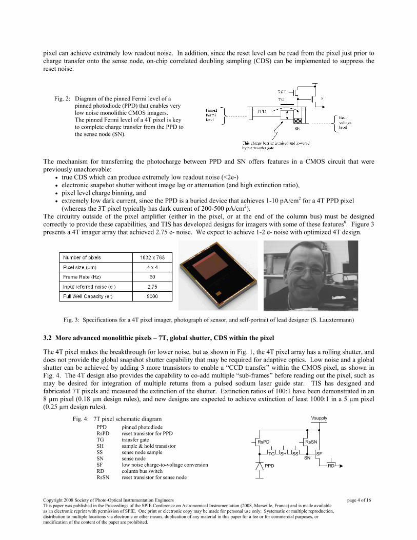
These arrays are made with relatively simple three transistor (or 3T) pixels, as shown in Fig. 1(a). One transistor is used to convert the charge-to-voltage and buffers the signal for readout, a second transistor resets the integration node, and the third transistor connects the pixel signal to the column bus of the multiplexer. While the imagers listed in Table 2 have served their intended application, these image arrays do not have the low noise and high quantum efficiency (QE) required for faint light level astronomy applications. 3.1 Lowering the readout noise of monolithic CMOS imagers to the levels required by astronomy Until recently, CMOS imagers have been at a disadvantage relative to CCDs for readout noise, since the readout circuit that is typically used in CMOS pixels is inherently higher noise than a CCD amplifier. One reason for higher noise is the capacitance of the sense node of the conventional three transistor (3T) CMOS pixel. The photodiode capacitance is connected to the sense node during readout, which leads to lower conversion gain and hence higher input referred noise. In a conventional 3T pixel, shown in Fig. 1(a), the photocharge is integrated on the photodiode, PD. The photodiode, PD, is directly connected to the source follower, SF, and a reset transistor, RST. The combined capacitance of PD, SF gate and RST source defines the sense node capacitance, the inverse of which is the pixel level charge to voltage gain (responsivity). For a typical pixel size of 5 µm in a 0.25 µm CMOS image sensor process, the sense node capacitance is about 5 fF, corresponding to a responsivity of 32 µV/electron, which limits the lowest readout noise to about 10 electrons. Smaller pixels can achieve lower capacitance and lower noise, but at the expense of smaller dynamic range.
With the development of the four transistor (4T) pixel, monolithic CMOS can now achieve the lowest noise levels required by astronomy3,4,5. In a 4T pixel, shown in fig. 1(b), the photodiode is designed with a pinned Fermi level, i.e. it is a pinned photodiode, PPD. The photocharge collected on PPD is transferred to the sense node, SN, using a transfer gate, TG, in a process similar to charge transfer in CCDs. The “pinned Fermi level” is essential to the charge transfer since it sets the voltage level of the photodiode above the reset voltage level of the sense node, as shown in Fig. 2. All of the photocharge is transferred noiselessly, and once the transfer is made, the PPD is effectively disconnected from the SN. Since the SN can be made with very low capacitance, the responsivity (μV per electron) is very high, and the 4T
Fig. 1: Schematic diagram of CMOS pixels (a) three transistor – 3T (b) four transistor – 4T
Copyright 2008 Society of Photo-Optical Instrumentation Engineers This paper was published in the Proceedings of the SPIE Conference on Astronomical Instrumentation (2008, Marseille, France) and is made available as an electronic reprint with permission of SPIE. One print or electronic copy may be made for personal use only. Systematic or multiple reproduction, distribution to multiple locations via electronic or other means, duplication of any material in this paper for a fee or for commercial purposes, or modification of the content of the paper are prohibited.
page 4 of 16
pixel can achieve extremely low readout noise. In addition, since the reset level can be read from the pixel just prior to charge transfer onto the sense node, on-chip correlated doubling sampling (CDS) can be implemented to suppress the reset noise.
The mechanism for transferring the photocharge between PPD and SN offers features in a CMOS circuit that were previously unachievable:
• true CDS which can produce extremely low readout noise (<2e-) • electronic snapshot shutter without image lag or attenuation (and high extinction ratio), • pixel level charge binning, and • extremely low dark current, since the PPD is a buried device that achieves 1-10 pA/cm2 for a 4T PPD pixel
(whereas the 3T pixel typically has dark current of 200-500 pA/cm2). The circuitry outside of the pixel amplifier (either in the pixel, or at the end of the column bus) must be designed correctly to provide these capabilities, and TIS has developed designs for imagers with some of these features6. Figure 3 presents a 4T imager array that achieved 2.75 e- noise. We expect to achieve 1-2 e- noise with optimized 4T design.
Fig. 3: Specifications for a 4T pixel imager, photograph of sensor, and self-portrait of lead designer (S. Lauxtermann)
3.2 More advanced monolithic pixels – 7T, global shutter, CDS within the pixel The 4T pixel makes the breakthrough for lower noise, but as shown in Fig. 1, the 4T pixel array has a rolling shutter, and does not provide the global snapshot shutter capability that may be required for adaptive optics. Low noise and a global shutter can be achieved by adding 3 more transistors to enable a “CCD transfer” within the CMOS pixel, as shown in Fig. 4. The 4T design also provides the capability to co-add multiple “sub-frames” before reading out the pixel, such as may be desired for integration of multiple returns from a pulsed sodium laser guide star. TIS has designed and fabricated 7T pixels and measured the extinction of the shutter. Extinction ratios of 100:1 have been demonstrated in an 8 µm pixel (0.18 µm design rules), and new designs are expected to achieve extinction of least 1000:1 in a 5 µm pixel (0.25 µm design rules).
SN
PPD
RsPD
TG SH SS
Vsupply
RD
SF
RsSN
Fig. 4: 7T pixel schematic diagram
PPD pinned photodiode RsPD reset transistor for PPD TG transfer gate SH sample & hold transistor SS sense node sample SN sense node SF low noise charge-to-voltage conversion RD column bus switch RsSN reset transistor for sense node
Fig. 2: Diagram of the pinned Fermi level of a pinned photodiode (PPD) that enables very low noise monolithic CMOS imagers. The pinned Fermi level of a 4T pixel is key to complete charge transfer from the PPD to the sense node (SN).

Copyright 2008 Society of Photo-Optical Instrumentation Engineers This paper was published in the Proceedings of the SPIE Conference on Astronomical Instrumentation (2008, Marseille, France) and is made available as an electronic reprint with permission of SPIE. One print or electronic copy may be made for personal use only. Systematic or multiple reproduction, distribution to multiple locations via electronic or other means, duplication of any material in this paper for a fee or for commercial purposes, or modification of the content of the paper are prohibited.
page 5 of 16
3.2 Development of monolithic CMOS laser guide star wavefront sensor detector for the ELTs Teledyne Imaging Sensors has commenced development of a monolithic CMOS image array that is optimized for Shack-Hartmann wavefront sensing of a sodium laser guide star (LGS) on an Extremely Large Telescope (ELT). The initial development goal is to demonstrate a monolithic CMOS design that can achieve 1-2 e- readout noise at 700 Hz frame rate. This design will first be tested in a small array in 2009. This development is planned to lead to a large array with the following specification: 1700×1700 pixels, 700 Hz frame rate, 1-2 e- noise, digital output (ADCs on chip), 80% QE at the 589 nm wavelength of LGS using an optimized microlens array (as described in the next section). 3.3 Improving the quantum efficiency of monolithic CMOS imagers The QE of monolithic CMOS is much lower than hybrid CMOS and backside illuminated CCDs for several reasons: (a) low fill factor of the photodiode in the pixel (~30%), (b) moderate quality of microlenses used to concentrate the light onto the photodiode, and (c) relatively thin absorption depth of the photodiode (3-5 µm). Frontside illuminated CMOS typically achieves a peak QE of about 65%, as shown in Fig. 5. TIS and other groups are working to achieve much higher QE from monolithic CMOS. Two approaches are being pursued:
1. Optimized microlens design with high resistivity silicon wafers • TIS has developed a microlens design that will deliver more than 80% of the incident light into the CMOS
photodiode. Combined with high resistivity silicon wafers that provide deep depletion and high NIR QE, this approach will provide high QE over wide bandpass. This microlens design approach requires a slow optical beam (f/10). The predicted QE curve from this approach is shown in Fig. 5.
2. Backside illuminated CMOS imagers • Backside illuminated CMOS is being pursued by several companies, for both commercial and scientific
applications. An example of the QE that can be achieved is demonstrated by data from IMEC (see Fig. 5).
Fig. 5: QE of monolithic CMOS imagers. Frontside illuminated imagers require microlenses for good QE. An optimized microlens has been modeled that, when combined with thick high resistivity silicon wafers, should achieve high QE across a wide bandpass. Note that this microlens design assumes a relatively slow input optical beam (f/10). Backside illuminated CMOS will provide high QE as achieved for backside illuminated CCDs. Best data yet published is from IMEC7.

Copyright 2008 Society of Photo-Optical Instrumentation Engineers This paper was published in the Proceedings of the SPIE Conference on Astronomical Instrumentation (2008, Marseille, France) and is made available as an electronic reprint with permission of SPIE. One print or electronic copy may be made for personal use only. Systematic or multiple reproduction, distribution to multiple locations via electronic or other means, duplication of any material in this paper for a fee or for commercial purposes, or modification of the content of the paper are prohibited.
page 6 of 16
4. HYBRID SILICON PIN CMOS IMAGE SENSORS AT TIS Teledyne has been producing silicon-based hybrid CMOS FPA since the late 1990’s8,9. The hybrid CMOS sensor possesses all of the monolithic CMOS functionalities and offers added advantages, including high fill factor, high QE, broadband sensitivity, high shutter extinction, and additional room in each pixel for signal processing. The hybrid CMOS FPA enables independent optimization of the detector array and the ROIC. Readout commonality with IR channels is an added advantage for instruments that use both visible and IR FPAs, simplifying system integration. Teledyne’s hybrid CMOS silicon detector FPA technology, called HyViSI™ (Hybrid Visible Silicon Imager), has established a FPA product line that offers detectors for soft X-ray, UV, visible, and near IR (NIR) wavelengths. Table 3 provides a partial list of ROICs used to produce HyViSI FPAs, and Fig. 6 shows the HyViSI development chronology.
TCM6604A TCM8050A H1RG-18 H2RG-18 H4RG-10
Pixel amplifier CTIA DI SF SF SF
Array Format (pixels) 640 × 480 1024 × 1024 1024 × 1024 2048 × 2048 4096 × 4096
Pixel Pitch (μm) 27 18 18 18 10
Number of Outputs 4 4 1, 2, or 16 1, 4 or 32 1, 4, 16, 32 or 64
Pixel Rate (MHz) 8 6 0.1 to 5 0.1 to 5 0.1 to 5
Read Out Mode Snapshot Snapshot Ripple Ripple Ripple
Window Mode Programmable Full, 512, 256 Guide window Guide window Guide window
Charge Capacity (ke-) 700 3,000 100 100 100
Readout Noise (e-) <100 <300 <10 <10 <10
Power Dissipation (mW) <70 <100 <1 <4 <16
Table 3: Partial list of ROICs used for silicon PIN hybrid CMOS FPAs. SF = source follower, DI = direct injection, CTIA = capacitive transimpedance amplifier
TCM1717 128X12860 μm pitch
TCM6600 640X48027 μm pitch
Hawaii 1024X102418.5 μm pitch
1998 1999 2000 2001
Hawaii-2 2048X204818 μm pitch
2002
Hawaii-2RG 2048X204818 μm pitch
2003 2004 2005
2x2 Hawaii-2RG 4096X409618 μm pitch
2006 2007
Hawaii-4RG-10 4096X409610 μm pitch
Fig. 6: Development chronology of HyViSITM FPAs at TIS

Copyright 2008 Society of Photo-Optical Instrumentation Engineers This paper was published in the Proceedings of the SPIE Conference on Astronomical Instrumentation (2008, Marseille, France) and is made available as an electronic reprint with permission of SPIE. One print or electronic copy may be made for personal use only. Systematic or multiple reproduction, distribution to multiple locations via electronic or other means, duplication of any material in this paper for a fee or for commercial purposes, or modification of the content of the paper are prohibited.
page 7 of 16
4.1 Quantum Efficiency of HyViSI image arrays The silicon PIN detector array is backside illuminated with 100% optical fill-factor and operates in a fully depleted mode for achieving minimal lateral charge diffusion. Silicon is an excellent material for direct detection for photons from soft x-ray to the silicon cutoff wavelength in the NIR. Figure 7 shows the room temperature absorption depth of photons in silicon in the soft x-ray band and near UV to near infrared bands. Due to different absorption mechanisms, 5-10 keV x-rays and 850-1000 nm NIR light have a long absorption length in silicon (20-200 µm); while low energy x-rays and UV light are absorbed within 10 to 40 nm of the silicon surface. HyViSI detector arrays are produced with thickness of 50 to 250 µm. In the surface region, minimization of dead layer and recombination loss is critical for low energy x-rays and UV light. With fully depleted operation and an optimized backside surface, the internal QE can be nearly 100%.
0.001
0.01
0.1
1
10
100
1000
100 1000 10000
Photon Energy, eV
Abs
orpt
ion
Dep
th, μ
m
Fig. 7: Absorption depth of photons in silicon as a function of: (a) X-ray energy and, (b) the wavelengths from UV to NIR
4.1.1 X-ray response
A high performance x-ray astronomy detector should achieve high QE and good energy resolution. TIS has developed a back surface process that provides internal QE above 90% in the UV. The low loss surface region provides good response to low energy x-ray photons (<500 eV). Since optical light is a noise source for x-ray astronomy, an optical blocking filter is typically used for x-ray applications. In a joint effort10, Penn State University and Teledyne Imaging Sensors have successfully applied an aluminum (Al) filter directly on the detector surface. Figure 8 shows a 1024×1024 pixel array with a 50 nm thick Al blocking filter covering half of the active area of the detector surface. With flat-field illumination by a Fe55 x-ray source and 700 nm optical source, this test detector measured the optical blocking of the filter as ~1000:1, and transmission of x-rays through the filter at nearly 100%. The Al filter thickness can be adjusted to optimize the tradeoff between optical blocking and low energy x-ray transmission. No optical AR coating was used on the array shown in Fig. 8 because an AR coating would absorb x-rays and reduce x-ray detection efficiency.
0.001
0.01
0.1
1
10
100
1000
200 300 400 500 600 700 800 900 1000 1100
wavelength, nm
Abs
orpt
ion
Dep
th, μ
m
Fig. 8: Photo of a HyViSI array with 50 nm Al blocking filter and the flat field responses to Fe55 x-rays and 700 nm optical illumination. Only the central 100×100 pixels are shown in the response images, so that the x-ray events are visible. The FPA was operated at 150K.
(a) (b)

Copyright 2008 Society of Photo-Optical Instrumentation Engineers This paper was published in the Proceedings of the SPIE Conference on Astronomical Instrumentation (2008, Marseille, France) and is made available as an electronic reprint with permission of SPIE. One print or electronic copy may be made for personal use only. Systematic or multiple reproduction, distribution to multiple locations via electronic or other means, duplication of any material in this paper for a fee or for commercial purposes, or modification of the content of the paper are prohibited.
page 8 of 16
4.1.2 Spectral QE from UV to NIR
The TIS HyViSI detector array is optimized so that the dominant QE loss mechanism is external optical reflection, which can be minimized with a proper AR coating design. Figure 9 presents spectral QE data measured on devices with various antireflection coatings, which TIS can optimize for specific application needs. High QE has been demonstrated over 200-1050 nm. QE in the vacuum UV (λ < 200 nm) has not yet been measured.
The temperature dependence of QE near the cutoff wavelength of silicon is of particular interest for applications that require a high NIR response at cryogenic operation. This dependence is a fundamental property of silicon and has been measured for 163K to 293K, as shown in Fig. 9.
Fig. 9: (a) Measured spectral QE from UV to NIR, and (b) measured temperature dependence of NIR QE. Quantum yield of greater than 1 below 330 nm has been taken into account, so that QE is the percentage of incoming photons detected.
4.2 Silicon PIN dark current
Dark current in the detector is due to thermal charge carrier generation in the depletion region and at the surfaces of the detector. Defects in the bulk silicon and at the surface will cause an excessive amount of dark current. TIS has an active internal research & development (IR&D) project to identify the process steps that cause dark current and modify the HyViSI detector processing as required. At present, the HyViSI dark current is 5-10 nA/cm2 at room temperature (298K), as shown in Fig. 10 for an 18 µm pixel. The IR&D project continues through 2008, with the goal of reducing dark current to ~1 nA/cm2.
0
10
20
30
40
50
60
70
80
90
100
200 300 400 500 600 700 800 900 1000 1100Wavelength (nm)
QE
(%)
Far UV Design
Near UV Design
Blue Design
NIR Design
Visible NIRUV
0.0001
0.001
0.01
0.1
1
10
100
1000
10000
100000
1000000
120 140 160 180 200 220 240 260 280 300
Temperature, K
Dar
k C
urre
nt, e
-/s/p
H2RG HyViSI2048x2048, 18μm pixelFig. 10: HyViSI dark current – 2008 baseline process
Dark current of HyViSI is 5-10 nA/cm2 at room temperature (298K), which corresponds to 1 e- per 18 µm pixel per sec at ~195K.
The IR&D project for dark current reduction continues through 2008, with goal to reduce room temperature dark current to ~1 nA/cm2.
0
10
20
30
40
50
60
70
80
90
100
850 900 950 1000 1050 1100Wavelength, nm
QE,
%
293K, Model293K, Measurement253K, Model253K, Measurement213K, Model213K, Measurement163K, Model163K, Measurement
(a) (b)

Copyright 2008 Society of Photo-Optical Instrumentation Engineers This paper was published in the Proceedings of the SPIE Conference on Astronomical Instrumentation (2008, Marseille, France) and is made available as an electronic reprint with permission of SPIE. One print or electronic copy may be made for personal use only. Systematic or multiple reproduction, distribution to multiple locations via electronic or other means, duplication of any material in this paper for a fee or for commercial purposes, or modification of the content of the paper are prohibited.
page 9 of 16
4.3 Silicon PIN charge diffusion With a thick detector layer, the pixels of a HyViSI array must have a strong electric field within the detector layer to push the photocharge to the p-n junction to minimize charge diffusion and obtain a good point spread function (PSF). The HyViSI arrays apply this field by a contact to the back surface that enables a bias of up to 50 volts to be applied. Figure 11 presents HyViSI charge diffusion as a function of detector bias voltage and detector thickness.
4.4 Silicon PIN readout noise
The source follower (SF) is a low noise pixel design widely used for low flux, long exposure applications such as astronomy. Fig. 12 shows the single CDS noise data measured as a function of temperature on several SF-based HyViSI FPAs. A HyViSI FPA with a SF can expect a single CDS noise of 7-10 e- rms at a pixel readout rate of 100 kHz, and operating temperature below 200K. The conversion gain was verified with Fe55 x-rays and is typically ~10 µV/e-.
4.5 Performance of HyViSI with a source follower amplifier The combination of a silicon PIN detector and a source follower (SF) readout pixel results in a sensor that has two limitations that affect performance. TIS is developing new detector and ROIC designs that address these effects, but users of existing arrays should be aware of them. These effects are not present in CTIA-based pixels (CTIA = capacitive transimpedance amplifier). 4.5.1 Interpixel Capacitance (IPC) For CMOS arrays made with source follower pixels, the gate of the SF of one pixel is capacitively coupled to some degree to the SF in each of its neighboring pixels12. Since the voltage on a SF gate changes as photocharge is accumulated, this voltage change will modify the voltage on neighboring pixels, causing an electrical crosstalk between
0
5
10
15
20
25
30
35
40
45
50
0 5 10 15 20 25 30Detector Bias, V
FWH
M, μ
m
100 um thick detector
75 um thick detector
50 um thick detector
Temp =300K
Fig. 11: Charge diffusion in HyViSI detector arrays
The full width half maximum (FWHM) of charge diffusion decreases with higher bias, and a FWHM much smaller than the pixel pitch can be achieved, even though the pixel aspect ratio is more than a factor of 5 (100 µm thick detector with 18 µm pixel).
0
5
10
15
20
25
30
35
40
20 40 60 80 100 120 140 160 180 200 220 240Temperature, K
CD
S N
oise
, rm
s e-
H2RG HyViSI
H1RG HyViSI
H-1 HyViSI
Fig. 12: Single CDS noise as measured using astronomy HyViSI FPAs, with a source follower amplifier in each pixel.
Readout noise (single CDS) of 7-10 e- can be expected with the H1RG or H2RG below 200K. Because of the nondestructive readout nature of SF ROIC, multiple samples can be used to further lower the read noise. Noise of less than 2 e- rms has been measured using 16 Fowler samples11.

Copyright 2008 Society of Photo-Optical Instrumentation Engineers This paper was published in the Proceedings of the SPIE Conference on Astronomical Instrumentation (2008, Marseille, France) and is made available as an electronic reprint with permission of SPIE. One print or electronic copy may be made for personal use only. Systematic or multiple reproduction, distribution to multiple locations via electronic or other means, duplication of any material in this paper for a fee or for commercial purposes, or modification of the content of the paper are prohibited.
page 10 of 16
pixels. This crosstalk occurs after charge collection and during the charge-to-voltage conversion process. The charge coupling for the 18 µm pixels of H1RG and H2RG HyViSI arrays has been reported to be 8-10% to nearest neighbors. One approach to remove interpixel coupling effects is to post-process the images using de-convolution. Since interpixel capacitance is a deterministic process, deconvolution can improve spatial resolution and x-ray event characterization. The Pennsylvania State University has demonstrated this by using a Lucy-Richardson algorithm to process HyViSI images13. Another approach is to reduce the interpixel coupling in the FPA by modifying the pixel design. Recently, TIS reported14 the results of design changes that reduced the coupling by a factor of 2 to 3, to 3.4%. The coupling was computed from autocorrelations of flat fields. The IPC reduction was verified by measuring the total pixel crosstalk with a pinhole measurement technique. Optical pinholes of various sizes were applied to the backside of HyViSI array, and crosstalk was measured at 600 and 900 nm; see Fig. 13. Although it is not possible to achieve ideal point source illumination, crosstalk for a point source response was estimated from the asymptote of the plot. For the SF detector array shown in Fig. 13, the total point source crosstalk reaches ~5% at 18V. Using a Gaussian function, the pixel crosstalk due to charge diffusion in the detector is ~1.5% at 180K and 18V bias. The crosstalk that remains is ~3.5%, which is in reasonable agreement with the coupling data derived from autocorrelation analysis.
0%
2%
4%
6%
8%
10%
12%
14%
16%
0 5 10 15 20 25
Detector Bias, V
Cro
ssta
lk, %
600 nm
900 nm
Pinhole = 6 μm
SFD Input
0%
2%
4%
6%
8%
10%
12%
14%
16%
0 5 10 15 20
Pin hole size, micron
Cro
ssta
lk, %
600 nm
900 nm
SFD Input
Bias = 17.7 V
4.5.2 Permanent threshold shift to HyViSI arrays with source followers from supersaturated exposure A HyViSI array is typically biased (Vsub) at 5V to 30V to minimize charge diffusion in the detector layer. However, in the case of arrays with source follower amplifiers, a supersaturated exposure without resetting the sense node can cause a permanent change to the 3.3V CMOS ROIC. This effect is best understood by examination of the SF pixel schematic shown in Fig. 14. The sense node (gate of the source follower), Vd, is reset to ~0 volts at the beginning of each frame. During the exposure, the sense node collects holes and the voltage on the sense node increases. The source follower will saturate when the voltage of the sense node reaches ~1V, which corresponds to ~100,000 electrons.
The gate oxide of the source follower has a minimum rated breakdown voltage of ~5.2V for the standard CMOS process. If the pixel is highly oversaturated, Vd will rise toward Vsub and the breakdown voltage can be exceeded, putting stress on the gate oxide. This stress can permanently change the source follower response, manifested as a threshold shift (change in DC level of output). This threshold shift is correctable with CDS processing, but the threshold shift results in
Fig. 14: Simplified schematic diagram of the H1RG and H2RG 3T pixel designs.
The reset voltage is ~0 volts.
Fig. 13: Crosstalk to each of four neighboring pixels measured as a function of detector bias for an 18 µm pixel source follower array with operating temperature of 180K. This data is for a new pixel design that reduces IPC so that coupling to nearest neighbor is ~3.5%.

Copyright 2008 Society of Photo-Optical Instrumentation Engineers This paper was published in the Proceedings of the SPIE Conference on Astronomical Instrumentation (2008, Marseille, France) and is made available as an electronic reprint with permission of SPIE. One print or electronic copy may be made for personal use only. Systematic or multiple reproduction, distribution to multiple locations via electronic or other means, duplication of any material in this paper for a fee or for commercial purposes, or modification of the content of the paper are prohibited.
page 11 of 16
loss of dynamic range of the affected pixels in the array. Supersaturation, for which the breakdown voltage is exceeded, is a function of actual breakdown voltage, detector bias, temperature, input light level, integration time, and frame rate (i.e. time between resets of the sense node). The supersaturation level is much higher than simple analysis suggests, since the pixel provides a leakage path that can limit the node voltage. Measurements indicate that supersaturation is at least 10× pixel full well, and in some cases is more than 100× full well.
TIS recommends the following measures to avoid supersaturation: • Either bias the detector at 5V (so that the breakdown voltage cannot be exceeded, no matter the flux level), or • avoid highly oversaturating the HyViSI array (ensure saturation does not exceed 10× full well), and
continuously reset the source follower amplifiers that are not being used for image integration.
TIS is investigating design changes that would place a permanent protection circuit in the pixels to eliminate the potential for exceeding the breakdown voltage. The protection circuitry would also provide anti-blooming control useful for imaging fields with high dynamic range (e.g. bright stars and faint galaxies). Note that CDS processing is required to remove any threshold shift caused by supersaturation. Also, note that this potential for damage only affects source follower readouts with silicon PIN arrays operated with high detector bias. CTIA-based pixels do not have threshold shift, since the sense node of a CTIA is held at constant bias. None of the TIS IR arrays that use source follower amplifiers have a risk of exceeding the breakdown voltage, since IR arrays operate with a small reverse bias (<1V). 4.6 New HyViSI arrays in development for astronomy TIS has two active developments for new HyViSI arrays for astronomy:
• High speed, low noise array with event detection for x-ray astronomy (also useful for wavefront sensing) • Large 4K×4K, 10 µm array
4.6.1 High speed, low noise, event driven readout for x-ray spectroscopy Silicon is an excellent sensor for soft x-rays (100 eV to 10 keV) since each x-ray will create many charge pairs in the silicon. The electron-hole pair generation in silicon by x-rays has a charge conversion factor of ~1e-/3.65 eV (quantum yield >1 commences at ~330 nm). For example a 5.9 keV Kα x-ray from an Fe55 source will produce an average of 1620 electrons in silicon for each absorbed photon. If the readout noise is low enough, the energy of each x-ray can be measured, so that the detector array is an imager and spectrograph at the same time.
TIS has developed a new high speed, low noise ROIC called Speedster128™ for adaptive optics and interferometry. The Speedster128 array has 128×128 pixels with 40 µm pitch. Each pixel contains a low noise CTIA and CDS processing. The array reads out a single analog port at up to 900 Hz frame rate. The predicted noise for this array is <4 e- for HyViSI and <5 e- for an IR detector (lower noise for silicon PIN due to lower detector pixel capacitance). This array has

Copyright 2008 Society of Photo-Optical Instrumentation Engineers This paper was published in the Proceedings of the SPIE Conference on Astronomical Instrumentation (2008, Marseille, France) and is made available as an electronic reprint with permission of SPIE. One print or electronic copy may be made for personal use only. Systematic or multiple reproduction, distribution to multiple locations via electronic or other means, duplication of any material in this paper for a fee or for commercial purposes, or modification of the content of the paper are prohibited.
page 12 of 16
a digital input, with clocks and biases generated on-chip. The Speedster128 is currently in fabrication, and the first hybrids will tested by the end of 2008. Future x-ray telescopes will have large fields of view, but x-ray events will be sparse, and fast readout of very large arrays is inefficient and limits the time resolution and flux of x-ray events. With an “event driven” CMOS readout, only the individual pixels which detect x-rays are read out. Since the readout rate can be very fast, the effective frame time can be very short, which is better for science and also reduces the effect of dark current, allowing operation at higher temperature. In collaboration with The Pennsylvania State University, Teledyne is developing the next generation x-ray detector for space astronomy. The first step will be to fabricate and test the Speedster128 array with the Al light shield, followed by a modification of the Speedster128 design to provide event driven readout. TIS has already demonstrated event driven readout during a collaboration with the Ball Aerospace & Technologies Corporation (BATC). In preparation for a proposal for the Geostationary Lightning Mapper (GLM), BATC and TIS developed an event driven readout that provided more functionality than required for x-ray detection. The requirement was to detect lightning events for both the sunlit and dark sides of the visible face of the Earth from geosynchronous orbit. Thus, the GLM test chip included analog subtraction of the background image, and detected events that were a programmable threshold above the background level. The array can be programmed to read out the 8 neighboring pixels of each event so that low level signal (from split events) is also recorded. The ROIC was fabricated and hybridized to a HyViSI array to demonstrate the proper functioning of the array at 2 kHz frame rate. Event driven detection is a key differentiator between CCD and CMOS readouts, and should be useful for a variety of applications. 4.6.2 Large format, small pixel H4RG-10 HyViSI array In 2006, TIS developed the first prototype 16.7 million pixel HyViSI arrays in a 4096×4096, 10 µm pixel format. The new ROIC is called the H4RG-10 (“4” stands for 4096×4096 pixels, and “-10” denotes the 10 μm pixel pitch). The H4RG-10 retains all the features and heritage of its highly successful predecessor, the H2RG readout multiplexer, and the design is scalable to an array format up to 16K×16K. In this development effort, TIS validated all ROIC functionality and established the manufacturing process for producing large hybrid arrays with small pixels. The prototype arrays demonstrated a high pixel interconnectivity (>99.9%) and high pixel operability (>99.8%), with a single CDS noise of 7 e- rms15. Figure 16 presents the connectivity map and histogram of a 4K×4K H4RG-10 hybrid. A newer version of the H4RG-10 ROIC has been fabricated and new H4RG-10 HyViSI hybrids will be made and tested during 2008.
Fig. 16: Electrical interconnect map and histogram of H4RG-10 FPA

Copyright 2008 Society of Photo-Optical Instrumentation Engineers This paper was published in the Proceedings of the SPIE Conference on Astronomical Instrumentation (2008, Marseille, France) and is made available as an electronic reprint with permission of SPIE. One print or electronic copy may be made for personal use only. Systematic or multiple reproduction, distribution to multiple locations via electronic or other means, duplication of any material in this paper for a fee or for commercial purposes, or modification of the content of the paper are prohibited.
page 13 of 16
4.7 HyViSI applications in astronomy and civil space Teledyne’s HyViSI arrays have made significant advancements recently, including:
• Operation in the Mars Reconnaissance Orbiter – 640×480 pixel array for spectroscopy • Integration into the Orbiting Carbon Observatory (Dec. 2008 launch) – 1024×1024 pixel array for spectroscopy • Nighttime telescope observations – 1K×1K, 2K×2K and 4K×4K pixel arrays
The following figures provide information on these applications.
Fig. 17: CRISM (Compact Reconnaissance Imaging Spectrometer for Mars) CRISM is a hyperspectral imager that is operating on the Mars Reconnaissance Orbiter since September 2006. The spectral range of the CRISM instrument spans the UV to the mid-wave IR; 360-3920 nm at 6.55 nm/channel and 20 meter resolution on the Mars surface, enabling identification of a broad range of minerals on the Martian surface. Within CRISM, light is split into VNIR (visible-near IR) (λ <= 1.05 μm) and MWIR (mid-wave IR) (λ >= 1.05 μm) beams. Two Teledyne FPAs are used for CRISM: VNIR FPA (HyViSI) and the IR FPA (HgCdTe). Both FPAs use the same 640×480 pixel CMOS ROIC. The VNIR focal plane assembly is shown at right. Teledyne Imaging Sensors also fabricated the order sorting filters used for both the VNIR and IR arrays. Teledyne Judson Technologies developed the thermoelectrically cooled, hermetically sealed package and integrated the focal plane assemblies.
Fig. 18: Orbiting Carbon Observatory (OCO) OCO is a NASA mission that will provide precise, time-dependent global measurements of atmospheric carbon dioxide (CO2) from a low Earth orbit satellite and enable more reliable forecasts of future changes to the Earth’s climate. OCO has three high-resolution spectrometers, each detecting a relatively small band of electromagnetic radiation (0.760 μm, 1.61 μm and 2.06 μm), as shown at right.
Three Teledyne H1RG-18 FPAs are integrated in the OCO instrument: one HyViSI FPA for measuring the O2 band and two HgCdTe SWIR FPAs for measurement of the CO2 bands. OCO launch is planned for December 2008, with a planned operational lifetime of 2 years.
Fig. 19: SOLIS (Synoptic Optical Long-term Investigations of the Sun) SOLIS is a ground-based synoptic solar observation project of the National Solar Observatory (NSO). The main instrument of SOLIS is the Vector Spectro Magnetograph (VSM); a compact, high-throughput vector-polarimeter. VSM is made of two high-speed cameras based on TIS 1K×1K format high-speed HyViSI focal plane arrays (bottom right). The VSM measures the photospheric magnetic field strength and direction over the full solar disk at three critical wavelengths: Fe-I 630.2 nm full-disk photospheric vector magnetograms, Ca-II 854.2 nm chromospheric longitudinal magnetograms and He-I 1083 nm spectroheliograms. The VSM instrument has been recording photospheric and chromospheric magnetograms daily since August 2003. The full-disk photospheric vector magnetogram image at right was taken in October 2003 during an exceptionally active solar flare period.

Copyright 2008 Society of Photo-Optical Instrumentation Engineers This paper was published in the Proceedings of the SPIE Conference on Astronomical Instrumentation (2008, Marseille, France) and is made available as an electronic reprint with permission of SPIE. One print or electronic copy may be made for personal use only. Systematic or multiple reproduction, distribution to multiple locations via electronic or other means, duplication of any material in this paper for a fee or for commercial purposes, or modification of the content of the paper are prohibited.
page 14 of 16
5. RADIATION EFFECTS ON CMOS IMAGERS
CMOS ROICs are inherently radiation hard due to the thin oxides used in fabrication and the FPAs do not suffer from charge transfer inefficiency that is problematic for CCDs. Radiation testing has shown the H2RG-18 to operate well in radiation levels far above the 50 krad requirement for the James Webb Space Telescope17,18. Very hard ROICs can be made with a “radiation hard by design” approach that TIS has developed. The silicon detector material damage depends on the type of radiation, but in general, QE does not suffer since the detectors are fully depleted and all charge that is generated is collected at the p-n junction. More problematic is the increase in dark current that occurs from displacement damage in the bulk silicon19. The proposed missions to Jupiter will encounter very high radiation environments and TIS can be contacted for further information about our capabilities in this area.
6. SUMMARY Teledyne Imaging Sensors is strongly committed to providing the highest performance silicon-based image arrays to the astronomical community. Monolithic CMOS imagers are approaching the quality required for astronomy, as the QE limitation of monolithic CMOS is being addressed and new very low noise readouts are being developed. A new monolithic CMOS wavefront sensor detector has been funded for development for ELT laser guide star systems. In parallel, TIS continues to improve the performance of its silicon PIN hybrid CMOS technology, named HyViSITM. HyViSI has unique features that cannot be provided by either monolithic CMOS or CCDs. The dark current of HyViSI
The Crab Nebula (M1)
1Kx1K H1RG-18 HyViSI
NGC2683 Spiral Galaxy
2Kx2K H2RG-18 HyViSI
The Hercules Cluster (M13)
4Kx4K H4RG-10 HyViSI
Fig. 20: Ground-based telescope observations Telescope observations are critical in evaluation of imaging sensors for astronomical applications. During 2007, three types of TIS HyViSI arrays (H1RG-18, H2RG-18, H4RG-10) were taken to telescopes for on-sky testing and characterization, including astrometric and photometric measurements15,16. The guide window mode of these FPAs was found to be very useful for telescope focusing and guiding. The images below were taken by the Rochester Imaging Detector Laboratory (RIDL) on the 2.1-meter telescope on Kitt Peak (Arizona). The images shown are composite images from three filters (I,G,Y). Each image is placed above the array that acquired the image.

Copyright 2008 Society of Photo-Optical Instrumentation Engineers This paper was published in the Proceedings of the SPIE Conference on Astronomical Instrumentation (2008, Marseille, France) and is made available as an electronic reprint with permission of SPIE. One print or electronic copy may be made for personal use only. Systematic or multiple reproduction, distribution to multiple locations via electronic or other means, duplication of any material in this paper for a fee or for commercial purposes, or modification of the content of the paper are prohibited.
page 15 of 16
has been reduced to 5-10 nA/cm2 and ongoing IR&D efforts aim to reduce dark current to 1 nA/cm2. New HyViSI arrays are being developed for astronomical applications: a high speed, low noise event driven readout for x-ray spectroscopy (and AO), and a large 4K×4K, 10 µm pixel array. TIS HyViSI arrays have reached NASA TRL-9, being used in the CRISM spectrometer that has been operating in the Mars Reconnaissance Orbiter since 2006. HyViSI arrays are also being tested by several ground-based observatories. With the capabilities provided by CMOS readout circuits and its low power and radiation hard capabilities, CMOS arrays (both monolithic and hybrid) will continue to find increased use in the astronomical community.
ACKNOWLEDGEMENTS The authors wish to acknowledge valuable discussions and fruitful collaborations with several colleagues in the astronomical community. X-ray detector development reported in this paper was a joint effort with Pennsylvania State University with funding from the NASA ROSS program. Technical discussions and data exchange with the Rochester Imaging Detector Laboratory at Rochester Institute of Technology and the Detector Characterization Laboratory at NASA Goddard Space Flight Center have been valuable to HyViSI FPA development.
REFERENCES [1] J.W. Beletic, R. Blank, D. Gulbransen, D. Lee, M. Loose, E.C. Piquette, T. Sprafke, W.E. Tennant, M. Zandian,
and J. Zino, “Teledyne Imaging Sensors: Infrared imaging technologies for Astronomy & Civil Space”, Proceedings of the SPIE, Vol. 7201, June 2008.
[2] A. Joshi, D. Chiaverini, K. Jung, V. Douence, G. Wijeratne, G. Williams and M. Loose, “Scalable Architecture for Video-Rate CMOS Imaging System on a Chip”, Proceedings from IEEE International Workshop on CCD and AIS, June 9-11 2005, Nagano, Japan, 2005.
[3] P. Magnan, “Detection of visible photons in CCD and CMOS: a comparative view”, Nuclear Instruments and Methods in Physics Research A, pp. 199-212, 2003.
[4] J. Janesick, J. Andrews, T. Elliott, “Fundamental performance differences between CMOS and CCD imagers: Part I” , Proceedings of SPIE, vol. 6276, p. 62760M, 2006.
[5] J. Janesick, J. Andrews, J. Tower, M. Grygon, T. Elliott, J. Cheng, M. Lesser, J. Pinter, “Fundamental performance differences between CMOS and CCD imagers: Part II” , Proceedings of SPIE, vol. 6690, p. 669003, 2007.
[6] S. Lauxtermann, A. Lee, J. Stevens, A. Joshi, “Comparison of Global Shutter Pixels for CMOS Image Sensors”, 2007 International Image Sensor Workshop, June 7-10, 2007, Ogunquit, Maine USA, 2007.
[7] J. Bogaerts, K. De Munck, P. De Moor, D. Sabuncuoglu Tezcan, I. Ficai Veltroni, G. Lepage, C. Van Hoof, “Radiometric Performance Enhancement of Hybrid and Monolithic Backside Illuminated CMOS APS for Space-borne Imaging”, 2007 International Image Sensor Workshop, June 7-10, 2007, Ogunquit, Maine USA, 2007.
[8] Y. Bai, J.T. Montroy, J. D. Blackwell, M.C. Farris, L. J. Kozlowski, K. Vural, “Development of Hybrid CMOS Visible Focal Plane Arrays at Rockwell”, Proceedings of SPIE, Vol. 4028, pp. 174-182, April 2000.
[9] L. J. Kozlowski, Y. Bai; M. Loose, A. Joshi; G. W. Hughes; J. D. Garnett, “Large area visible arrays: performance of hybrid and monolithic alternatives”, Proceedings of SPIE, Vol. 4836, December 2002.
[10] A. D. Falcone, D. N. Burrowsa, Y. Bai, M. Farris, R. Cook, S. Bongiorno, “Hybrid CMOS X-ray Detectors: The Next Generation for Focused X-ray Telescopes”, Proceedings of SPIE, Vol. 6686, September 2007.
[11] R. J. Dorn; S. Eschbaumer, G. Finger, L. Mehrgan; M. Meyer, J. Stegmeier, “A CMOS visible silicon imager hybridized to a Rockwell 2RG multiplexer as a new detector for ground based astronomy”, SPIE, Vol. 6276, 2006.
[12] G. Finger, J. W. Beletic, R.J. Dorn, M. Meyer, L. Mehrgan, A. Moorwood and J. Stegmeier, “Conversion gain and interpixel capacitance of CMOS hybrid focal plane arrays”, Scientific Detectors for Astronomy, pp 477-490, 2005.
[13] S. Bongiorno, A. Falcone, D. Burrows, R. Cook, “Lucy-Richardson Deconvolution Applied To X-ray Hybrid CMOS Detector Data”, 10th AAS HEAD meeting, 2008.
[14] Y. Bai, M. C. Farris, A. K. Petersen, J. W. Beletic, “Inter-Pixel Capacitance in Fully Depleted Silicon Hybrid CMOS Focal Plane Arrays”, Proceedings of SPIE, Vol. 6690, 669004-8, August 2007.
[15] B. N. Dorland, et al, “Laboratory and Sky Testing for the TIS H4RG-10 4Kx4K, 10 micron pixel visible CMOS hybrid detector”, Proceedings of SPIE, vol. 6690, p. D-1, August 2007.
[16] Lance M. Simms; Donald F. Figer; Brandon J. Hanold; Daniel J. Kerr; D. Kirk Gilmore; Steven M. Kahn; J. Anthony Tyson, “First use of HyViSI H4RG for astronomical observations”, Proceedings of SPIE, vol. 6690, August 2007.

Copyright 2008 Society of Photo-Optical Instrumentation Engineers This paper was published in the Proceedings of the SPIE Conference on Astronomical Instrumentation (2008, Marseille, France) and is made available as an electronic reprint with permission of SPIE. One print or electronic copy may be made for personal use only. Systematic or multiple reproduction, distribution to multiple locations via electronic or other means, duplication of any material in this paper for a fee or for commercial purposes, or modification of the content of the paper are prohibited.
page 16 of 16
[17] M.E. McKelvey, K.A. Ennico, R.R. Johnson, P.W. Marshall, R.E. McMurray Jr., C.R. McCreight, J.C. Pickel, R.A. Reed, “Radiation Environment Performance of JWST Prototype FPAs”, SPIE 5167, pp223-234, 2004.
[18] P. Warren, S. DeWalt and M. Blouke, “Total Ionizing dose response results of the HAWAII-2RG focal plane array”, Proceedings of SPIE, Vol. 5902, pp. N1- N9, August 2005.
[19] R. Lowell1, C. Conger, S. Rainwater, M. Lazo, Y. Bai, “Rockwell H1RG silicon PIN diode array gamma and proton characterization at cryogenic temperatures”, Workshop Record of Nuclear and Space Radiation Effects Conference (NSREC). pp. 171-175, 2005.
This paper has been approved for public release by the DoD Office of Security Review (case #08-S-1768).
Copyright © 2022 FDOKUMEN