A versatile 3.3 V CMOS laser driver system
11
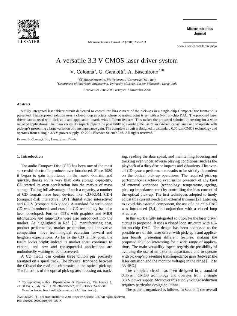
A versatile 3.3 V CMOS laser driver system V. Colonna a , G. Gandolfi a , A. Baschirotto b, * a ST Microelectronics, Via Tolomeo, 1-Cornaredo (MI), Italy b Department of Innovation Engineering, University of Lecce, Via per Monteroni, Lecce, Italy Received 21 June 2000; accepted 7 November 2000 Abstract A fully integrated laser driver circuit dedicated to control the bias current of the pick-ups in a single-chip Compact-Disc front-end is presented. The proposed solution uses a closed loop structure whose operating point is set with a 6-bit on-chip DAC. The proposed laser driver can be used with pick-up’s and application boards with different features. This makes the proposed solution interesting for a wide range of applications. The main versatility aspects regard the possibility of avoiding the use of an external capacitance and to operate with pick-up’s presenting a large variation of transimpedance gain. The complete circuit is designed in a standard 0.35 mm CMOS technology and operates from a single 3.3 V power supply. q 2001 Elsevier Science Ltd. All rights reserved. Keywords: Compact disc; Laser driver; Diode 1. Introduction The audio Compact Disc (CD) has been one of the most successful electronic products ever introduced. Since 1980 it began to gain importance in the music domain, and quickly, thanks to its very high data storage capability, CD started its own acceleration into the market of mass storage. Taking full advantage of such a capacity, a number of CD formats have been devised like: CD-ROM, CD-I (compact disk interactive), DVI (digital video interactive) and CD-V (compact disk video). A standard for write-once CD was introduced, and erasable CD technology has also been developed. Further, CD’s with graphics and MIDI information and mini-CD’s were also introduced into the market. As highlighted in Ref. [1], manufacturing cost, product performance, market penetration, and innovative competition move technological evolution forward and heighten expectations. As far as the CD family goes, the future looks bright; indeed its market share continues to expand, and new and consequential applications are undoubtedly waiting to be discovered. A CD media can contain three billion pits precisely arranged on a spiral track. The physical front-end between the CD and the read-out electronics is the optical pick-up. The functions of the optical pick-up are: focusing on, track- ing, reading the data spiral, and maintaining focusing and tracking even under adverse playing conditions, such as the playback of a dirty disc or impacts and vibrations. The over- all CD system performance results to be strictly dependent on the optical pick-up operations. The required pick-up performance is achieved even in the presence of any kind of external variations (technology, temperature, ageing, pick-up impedance, etc.) by controlling the bias current of the optical pick-up. The first techniques adopted to finely adjust this current needed an external trimmer [2]. Later on, to avoid this external component, the use of a on-chip DAC was introduced [3,4], in conjunction with a closed loop structure. In this work a fully integrated solution for the laser driver circuit is proposed. It uses a closed loop structure with a 6- bit on-chip DAC. The design has been addressed to the possible use of this laser driver with pick-up’s and applica- tion boards presenting different features, making the proposed solution interesting for a wide range of applica- tions. The main versatility aspect regards the possibility of avoiding the use of an external capacitance and to operate with pick-up’s presenting transimpedance gain (between the laser emission and the monitor voltage) in the range [22 to 33 dBV]. The complete circuit has been designed in a standard 0.35 mm CMOS technology and operates from a single 3.3 V power supply. Moreover this supply voltage reduction requires particular design solutions. The paper is organized as follows. In Section 2 the overall Microelectronics Journal 32 (2001) 253–263 Microelectronics Journal 0026-2692/01/$ - see front matter q 2001 Elsevier Science Ltd. All rights reserved. PII: S0026-2692(00)00135-X www.elsevier.com/locate/mejo * Corresponding author. Dipartimento di Electronica, Via Ferrata 1, 27100 Pavia, Italy. Tel.: 1390-382-502-227; fax: 1390-382-422-583. E-mail address: [email protected] (A. Baschirotto).
-
Upload
independent -
Category
Documents
-
view
0 -
download
0
Transcript of A versatile 3.3 V CMOS laser driver system
A versatile 3.3 V CMOS laser driver system
V. Colonnaa, G. Gandolfia, A. Baschirottob,*aST Microelectronics, Via Tolomeo, 1-Cornaredo (MI), Italy
bDepartment of Innovation Engineering, University of Lecce, Via per Monteroni, Lecce, Italy
Received 21 June 2000; accepted 7 November 2000
Abstract
A fully integrated laser driver circuit dedicated to control the bias current of the pick-ups in a single-chip Compact-Disc front-end ispresented. The proposed solution uses a closed loop structure whose operating point is set with a 6-bit on-chip DAC. The proposed laserdriver can be used with pick-up’s and application boards with different features. This makes the proposed solution interesting for a widerange of applications. The main versatility aspects regard the possibility of avoiding the use of an external capacitance and to operate withpick-up’s presenting a large variation of transimpedance gain. The complete circuit is designed in a standard 0.35mm CMOS technology andoperates from a single 3.3 V power supply.q 2001 Elsevier Science Ltd. All rights reserved.
Keywords: Compact disc; Laser driver; Diode
1. Introduction
The audio Compact Disc (CD) has been one of the mostsuccessful electronic products ever introduced. Since 1980it began to gain importance in the music domain, andquickly, thanks to its very high data storage capability,CD started its own acceleration into the market of massstorage. Taking full advantage of such a capacity, a numberof CD formats have been devised like: CD-ROM, CD-I(compact disk interactive), DVI (digital video interactive)and CD-V (compact disk video). A standard for write-onceCD was introduced, and erasable CD technology has alsobeen developed. Further, CD’s with graphics and MIDIinformation and mini-CD’s were also introduced into themarket. As highlighted in Ref. [1], manufacturing cost,product performance, market penetration, and innovativecompetition move technological evolution forward andheighten expectations. As far as the CD family goes, thefuture looks bright; indeed its market share continues toexpand, and new and consequential applications areundoubtedly waiting to be discovered.
A CD media can contain three billion pits preciselyarranged on a spiral track. The physical front-end betweenthe CD and the read-out electronics is the optical pick-up.The functions of the optical pick-up are: focusing on, track-
ing, reading the data spiral, and maintaining focusing andtracking even under adverse playing conditions, such as theplayback of a dirty disc or impacts and vibrations. The over-all CD system performance results to be strictly dependenton the optical pick-up operations. The required pick-upperformance is achieved even in the presence of any kindof external variations (technology, temperature, ageing,pick-up impedance, etc.) by controlling the bias current ofthe optical pick-up. The first techniques adopted to finelyadjust this current needed an external trimmer [2]. Later on,to avoid this external component, the use of a on-chip DACwas introduced [3,4], in conjunction with a closed loopstructure.
In this work a fully integrated solution for the laser drivercircuit is proposed. It uses a closed loop structure with a 6-bit on-chip DAC. The design has been addressed to thepossible use of this laser driver with pick-up’s and applica-tion boards presenting different features, making theproposed solution interesting for a wide range of applica-tions. The main versatility aspect regards the possibility ofavoiding the use of an external capacitance and to operatewith pick-up’s presenting transimpedance gain (between thelaser emission and the monitor voltage) in the range [22 to33 dBV].
The complete circuit has been designed in a standard0.35mm CMOS technology and operates from a single3.3 V power supply. Moreover this supply voltage reductionrequires particular design solutions.
The paper is organized as follows. In Section 2 the overall
Microelectronics Journal 32 (2001) 253–263
MicroelectronicsJournal
0026-2692/01/$ - see front matterq 2001 Elsevier Science Ltd. All rights reserved.PII: S0026-2692(00)00135-X
www.elsevier.com/locate/mejo
* Corresponding author. Dipartimento di Electronica, Via Ferrata 1,27100 Pavia, Italy. Tel.:1390-382-502-227; fax:1390-382-422-583.
E-mail address:[email protected] (A. Baschirotto).
architecture of the laser driver is proposed, giving detailsabout the effort in making the structure suitable for a largespread of possible pick-up’s. In Section 3 the digitalprogrammability of the laser driver features is described.In Section 4 details about the circuit solution for the singleblock are given, while Section 5 proposes the performanceachieved by the laser driver.
2. Proposed architecture
Any pick-up is composed of a low noise laser diode witha built-in monitor photo diode and some signal photodiodes. The light emitted by the laser diode is a functionof its bias current and it is monitored by the photo diodewhose output voltage is proportional to the light incident onit. One of the most important problems of laser diodes is thefact that the current vs. emitted-power characteristic canexhibit large variations (due to temperature and ageing) in
both the slope (that determine output power as a function ofmodulating waveform) and the threshold current (whichdetermines the laser effect point). Thus the emissionpower of the laser diode has to be stabilised.
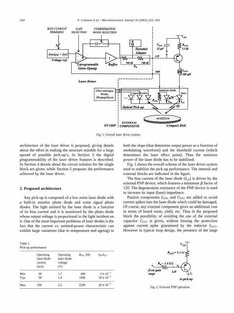
Fig. 1 shows the overall scheme of the laser driver systemused to stabilize the pick-up performance. The internal andexternal blocks are indicated in the figure.
The bias current of the laser diode (ILD) is driven by theexternal PNP device, which features a minimumb factor of120. The degeneration resistance of the PNP device is usedto increase its input (base) impedance.
Passive componentsLEXT and CEXT are added to avoidcurrent spikes into the laser diode which could be damaged.Of course, any external component gives an additional costin terms of board room, yield, etc. Thus in the proposedblock the possibility of avoiding the use of the externalcapacitor CEXT is given, without loosing the protectionagainst current spike guaranteed by the inductorLEXT.However in typical loop design, the presence of the large
V. Colonna et al. / Microelectronics Journal 32 (2001) 253–263254
Fig. 1. Overall laser driver system.
Table 1Pick-up performance
Operatinglaser diodecurrent(mA)
Operatinglaser diodevoltage(V)
RPOL (V) IPD/ILD
Min. 30 1.7 400 2× 10²³
Typ. 50 1.9 1000 10× 1023
Max. 100 2.5 2200 20× 1023
Fig. 2. External PNP operation.
external capacitorCEXT corresponds to the dominant pole,while, in the case of its absence, loop stability has to beensured in another way.
About the optical pick-ups, it is composed by a laserdiode (LD) and a monitor diode (MD). The power emittedby the laser diode is absorbed by the monitor diode andtranslated in the currentIPD which flows through internalresistor RPOL resulting in the output voltageMD �RPOLIPD: The amount of emitted power is controlled bythe laser diode bias currentILD. For typical pick-ups in themarket, the most common physical parameters are includedin ranges shown in Table 1.
The gain bias current-to-emitted power is not stable andtherefore it is not possible to operate the control giving afixed value of the bias current. On the other hand the gainemitted power-to-monitor diode voltage (MD) is verystable. The control of the emitter power can then be doneby proper setting the monitor diode voltage through a closedloop control circuit. The feedback loop forces the voltageacross the monitor diode at a constant level [5,6], and so alsothe light power emitted by the laser is properly set.
This solution allows to face the problem of operating withthe pick-up’s available in the market which exhibit differentfeatures. However as for any other closed loop structure, thestability of the system has to be guaranteed for any opera-tion condition. This means that a different loop gain valueshould be necessary to guarantee loop stability for anyadopted pick-up (featuring different pick-up gain value).The large spread of pick-up gain has been afforded in this
design by giving the possibility of a digital setting the inter-nal circuit gain, in order to ensure stability. Only two loopgain values have been necessary to guarantee stability forany pick-up whose transimpedance gainRLD (given byRPOLIPD/ILD, as shown later) is in the range [22 to33 dBV]. This range covers the major part of the pick-upsin the market.
The target of the proposed circuital block is the control ofthe optical pick-up light power emission. In addition, twoadditional features are given for the board designer:
• To give the possibility of using different pick-up with thesame board.
• To give the possibility of avoiding the use of externalcapacitorCEXT.
These features correspond to give the possibility of digitallycontrolling the pick-up bias current (this is done with a 6-bitaccuracy through a dedicated DAC), the control loop gain(via a single bit selector), and the dominant pole position(again with a single-bit selector).
As an additional feature of the proposed architecture, thepossibility of digitally controlling the pick-up current corre-sponds to give the possibility of turning-off the pick-up viasoftware, just selecting the value zero for its current level.
Since the system has to control the bias current of thepick-up, the band of the loop then has to be very small.However, the target accuracy (equivalent to the 6-bitDAC) requires a large loop gain, which should result ininstability in the presence of multiple gain stage in cascadein the loop. The overall gains of the loop and the dominantpole position then have to be studied.
With reference to scheme of Fig. 1, the small signal loop-gain transfer function of the complete system (GLOOP) can bewritten as:
GLOOP� GPNPRLDAOA �1�where GPNP is the transconductance gain due to externalPNP bipolar and resistor,RLD the transimpedance gain ofthe pick-up, andAOA is the gain of the operational amplifier.
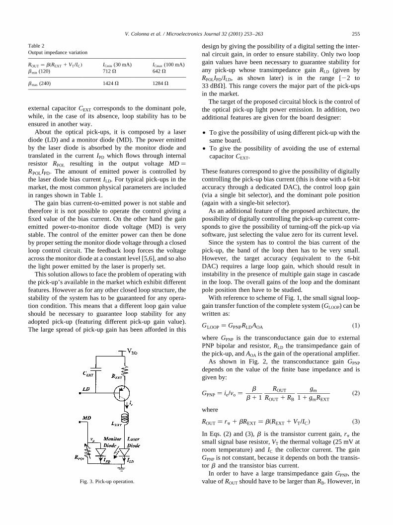
As shown in Fig. 2, the transconductance gainGPNP
depends on the value of the finite base impedance and isgiven by:
GPNP� ie=vo � b
b 1 1ROUT
ROUT 1 RB
gm
1 1 gmREXT�2�
where
ROUT � rp 1 bREXT � b�REXT 1 VT=IC� �3�In Eqs. (2) and (3),b is the transistor current gain,rp thesmall signal base resistor,VT the thermal voltage (25 mV atroom temperature) andIC the collector current. The gainGPNP is not constant, because it depends on both the transis-tor b and the transistor bias current.
In order to have a large transimpedance gainGPNP, thevalue ofROUT should have to be larger thanRB. However, in
V. Colonna et al. / Microelectronics Journal 32 (2001) 253–263 255
Table 2Output impedance variation
ROUT � b�REXT 1 VT=IC� ICmin (30 mA) ICmax (100 mA)bmin (120) 712V 642V
bmax (240) 1424V 1284V
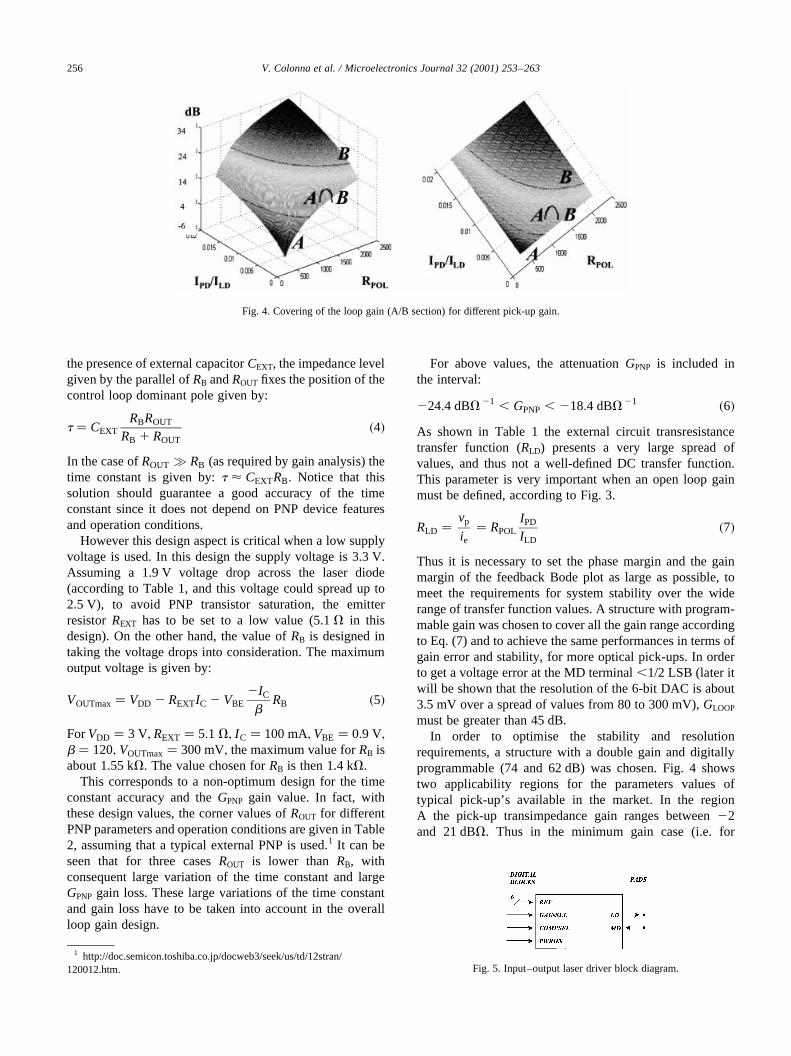
Fig. 3. Pick-up operation.
the presence of external capacitorCEXT, the impedance levelgiven by the parallel ofRB andROUT fixes the position of thecontrol loop dominant pole given by:
t � CEXTRBROUT
RB 1 ROUT�4�
In the case ofROUT q RB (as required by gain analysis) thetime constant is given by:t < CEXTRB: Notice that thissolution should guarantee a good accuracy of the timeconstant since it does not depend on PNP device featuresand operation conditions.
However this design aspect is critical when a low supplyvoltage is used. In this design the supply voltage is 3.3 V.Assuming a 1.9 V voltage drop across the laser diode(according to Table 1, and this voltage could spread up to2.5 V), to avoid PNP transistor saturation, the emitterresistorREXT has to be set to a low value (5.1V in thisdesign). On the other hand, the value ofRB is designed intaking the voltage drops into consideration. The maximumoutput voltage is given by:
VOUTmax� VDD 2 REXTIC 2 VBE2IC
bRB �5�
ForVDD � 3 V; REXT � 5:1V; IC � 100 mA; VBE � 0:9 V;b � 120; VOUTmax� 300 mV; the maximum value forRB isabout 1.55 kV. The value chosen forRB is then 1.4 kV.
This corresponds to a non-optimum design for the timeconstant accuracy and theGPNP gain value. In fact, withthese design values, the corner values ofROUT for differentPNP parameters and operation conditions are given in Table2, assuming that a typical external PNP is used.1 It can beseen that for three casesROUT is lower than RB, withconsequent large variation of the time constant and largeGPNP gain loss. These large variations of the time constantand gain loss have to be taken into account in the overallloop gain design.
For above values, the attenuationGPNP is included inthe interval:
224:4 dBV21 , GPNP , 218:4 dBV21 �6�As shown in Table 1 the external circuit transresistancetransfer function (RLD) presents a very large spread ofvalues, and thus not a well-defined DC transfer function.This parameter is very important when an open loop gainmust be defined, according to Fig. 3.
RLD �vp
ie� RPOL
IPD
ILD�7�
Thus it is necessary to set the phase margin and the gainmargin of the feedback Bode plot as large as possible, tomeet the requirements for system stability over the widerange of transfer function values. A structure with program-mable gain was chosen to cover all the gain range accordingto Eq. (7) and to achieve the same performances in terms ofgain error and stability, for more optical pick-ups. In orderto get a voltage error at the MD terminal,1/2 LSB (later itwill be shown that the resolution of the 6-bit DAC is about3.5 mV over a spread of values from 80 to 300 mV),GLOOP
must be greater than 45 dB.In order to optimise the stability and resolution
requirements, a structure with a double gain and digitallyprogrammable (74 and 62 dB) was chosen. Fig. 4 showstwo applicability regions for the parameters values oftypical pick-up’s available in the market. In the regionA the pick-up transimpedance gain ranges between22and 21 dBV. Thus in the minimum gain case (i.e. for
V. Colonna et al. / Microelectronics Journal 32 (2001) 253–263256
1 http://doc.semicon.toshiba.co.jp/docweb3/seek/us/td/12stran/120012.htm.
Fig. 4. Covering of the loop gain (A/B section) for different pick-up gain.
Fig. 5. Input–output laser driver block diagram.
RLD � 22 dBV21 and GPNP� 224:4 dBV21� a mini-mum AOA equal to 71.4 dB is needed, according to Eq.(1). Therefore in order to overcome the temperature andprocess worst cases a higher nominal gainAOA � 74 dBhas been designed. On the other hand, in region B thetransimpedance pick-up gainRLD ranges between 10 and
33 dBV. In this caseAOA � 62 dB is sufficiently large toguarantee the same requirements of resolution.Obviously, on the overlap of the two regions both config-uration gains can be utilised.
In regard to stability requirements the total open loop gainranges between 47.6 and 76.6 dB for both regions, and
V. Colonna et al. / Microelectronics Journal 32 (2001) 253–263 257
Fig. 6. Six-bit DAC structure.
Fig. 7. Internal or external compensation mode.
Fig. 8. Programmable gain opamp.
simulations show that the steady state is reached even inworst cases, for both internal and external compensationmode, as described in the following.
3. Digital programmable features
The proposed laser driver is embedded in a mixed signalCD system in which large part of the signal processing isdigital. Thus the full programmability of the laser driveroperation has to be carried out in a digital fashion.
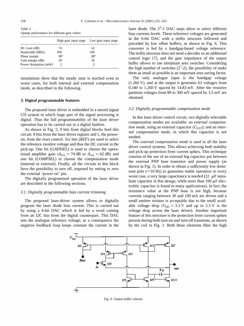
As shown in Fig. 5, 9 bits from digital blocks feed thiscircuit: 8 bits from the laser driver register and 1, the power-on, from the reset control. Six bits (REF) are used to selectthe reference monitor voltage and thus the DC current in thepick-up. One bit (GAINSEL) is used to choose the opera-tional amplifier gain�AOA � 74 dB or AOA � 62 dB� andone bit (COMPSEL) to choose the compensation mode(internal or external). Finally, all the circuits in this blockhave the possibility to turn off, imposed by setting to zerothe external ‘power on’ pin.
The digitally programmed operation of the laser driverare described in the following sections.
3.1. Digitally programmable bias current trimming
The proposed laser-driver system allows to digitallyprogram the laser diode bias current. This is carried outby using a 6-bit DAC which is fed by a word comingfrom an I2C bus from the digital counterpart. This DACsets the analogue reference voltage; as a consequence thenegative feedback loop keeps constant the current in the
laser diode. The 26-1 DAC steps allow to select differentbias currents levels. These reference voltages are generatedin the 6-bit DAC with a trellis structure followed andpreceded by low offset buffers, as shown in Fig. 6. Thisconverter is fed by a bandgap-based voltage reference.The trellis structure does not need a decoder or an additionalcontrol logic [7], and the gate impedance of the outputbuffer allows to use minimum area switches. Consideringthe high number of switches (27-2), the possibility of makethem as small as possible is an important area saving factor.
The only analogue input is the bandgap voltage(1.260 V), and at the output it generates 63 voltages from0.340 to 1.260 V spaced by 14.83 mV. After the resistivepartition voltages from 80 to 300 mV spaced by 3.5 mV areobtained.
3.2. Digitally programmable compensation mode
In this laser driver control circuit, two digitally selectablecompensation modes are available: anexternal compensa-tion mode, using an external capacitor (CEXT); and aninter-nal compensation mode, in which this capacitor is notneeded.
The external compensation modeis used in all the laserdriver control systems. This allows achieving both stabilityand pick-up protection from current spikes. This techniqueconsists of the use of an external big capacitor put betweenthe external PNP base transistor and power supply (asshown in Fig. 1). In order to obtain a sufficiently low domi-nant pole (<10 Hz) to guarantee stable operation in everyworst case, a very large capacitance is needed (22mF tanta-lium capacitor in this design, while more than 100mF elec-trolitic capacitor is found in many applications). In fact, theresistance value at the PNP base is not high, becausecurrents ranging between 30 and 100 mA are driven and asmall emitter resistor is acceptable due to the small avail-able voltage drop�VDD � 3:3 V and up to 2.5 V is thevoltage drop across the laser driver). Another importantfeature of this structure is the protection from current spikespresent during both turn-on and turn-off transients, as shownby the coil in Fig. 1. Both these elements filter the high
V. Colonna et al. / Microelectronics Journal 32 (2001) 253–263258
Table 3Opamp performance for different gain values
High gain input stage Low gain input stage
DC Gain (dB) 74 62Bandwidth (MHz) 450 100Phase margin 888 888
Gain margin (dB) 30 36Power dissipation (mW) 2 2
Fig. 9. Output buffer scheme.
frequencies spike currents coming in the laser diode, whichcould damage the laser diode.
The alternative internal compensation modeis hereproposed. Its conceptual scheme is shown in Fig. 7.The adopted technology allows the use of double-polycapacitor. Thus a high-value integrated capacitor doesnot have a very big impact on the silicon area. Withthe used amplification structure, only a 50 pF (whichrequires and area of 0.045 mm2) and a 2.5 pF integratedcapacitors are needed. Using a Miller circuit to multiplythe capacitor value, and an accurate study of turn-on andturn-off strategy, the big external capacitor may beavoided. The minimum dominant pole value achievable
with such capacitors is about 200 Hz, a sufficient valueconsidering the pole splitting effect.
It is possible to select the internal or the external compen-sation mode, including or excluding the integrated 50 pFcapacitor by a switch selection system controlled by onebit (COMPSEL).
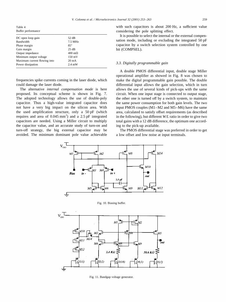
3.3. Digitally programmable gain
A double PMOS differential input, double stage Milleroperational amplifier as showed in Fig. 8 was chosen tomake the digital programmable gain possible. The doubledifferential input allows the gain selection, which in turnallows the use of several kinds of pick-ups with the samecircuit. When one input stage is connected to output stage,the other one is turned off by a switch system, to maintainthe same power consumption for both gain levels. The twoinput PMOS couples (M1–M2 and M5–M6) have the samearea, calculated to satisfy offset requirements (as describedin the following), but differentW/L ratio in order to give twototal gains with a 12 dB difference, the optimum one accord-ing to the pick-up available.
The PMOS differential stage was preferred in order to geta low offset and low noise at input terminals.
V. Colonna et al. / Microelectronics Journal 32 (2001) 253–263 259
Table 4Buffer performance
DC open loop gain 52 dBBandwidth 7.5 MHzPhase margin 858Gain margin 25 dBOutput impedance 400 mVMinimum output voltage 150 mVMaximum current flowing into 20 mAPower dissipation 2.4 mW
Fig. 10. Biasing buffer.
Fig. 11. Bandgap voltage generator.
4. Feedback loop circuit blocks
In the following paragraphs, some characteristics aboutthe circuits designed to compose the feedback loop areshown.
The main constraints about the amplification stages are: alow power consumption; a low offset input stage; a rela-tively high gain (<70 dB); and an output stage with groundcompatibility and big capability to drive currents flowinginto (up to 2 mA) from the external bipolar transistor. Inorder to get these requirements, the chosen structure is aMiller double stage single ended amplifier followed by anoutput buffer with both ground compatibility and big currentdriving capability. This way it is possible to unbind lowoffset requirements from external load constraints. In factthe output current does not affect the input stage because ofthe buffer, and the output voltage imposed by the externalcircuit does not affect the differential input stage thanks tothe second amplification stage.
4.1. Operational amplifier
The double stage Miller operational amplifier shown inFig. 8 has been adopted. The PMOS differential stage waspreferred to get a low offset and a low noise at input term-inals; other strategies were used to get very lowsystematicoffsetandprocess offset. To reduce the systematic offset acorrect biasing current ratio by the first stage NMOS and
second stage NMOS geometries for the first and secondamplification stages was used:
2Isecond stage=Ifirst stage� �W=L�M11��=�W=L�M4��� �W=L�M11��=�W=L�M9�� �8�
This equation guarantees saving the early effect on the firststage NMOS transistor, and a cancellation of systematicoffset. This is made possible because the output bufferdoes not require current from the second amplificationstage. The process offset can be expressed as follows:
VOS� DVTH 1 �VGS 2 VTH�=2��2DRL =RL�2 D�W=L�=�W=L���9�
This offset, which can be high in a full CMOS technology,has been minimised by adopting more strategies:
• Big active area input PMOS are used (both input PMOScouples have area is equal to 400mm2) in order to get asufficiently low DVTH (calculated to be,1.6 mV withprocess parameters).
• High resistive NMOS have been chosen for the differen-tial to single ended conversion. This is important in orderto obtain both a high gain in the first stage and a lowsensitivity to their mismatch at the input.◦ High first stage gain in order to reduce all offset
contributions from the other stages.◦ Low overdrive voltages.
V. Colonna et al. / Microelectronics Journal 32 (2001) 253–263260
Fig. 12. Layout of the overall laser driver circuit.
Using the above solutions the total offset is kept lower than10 mV.
The main features of the operational amplifier in the inter-nal compensation mode (i.e. with the 50 pF compensationcapacitor) are given in Table 3. The extremely large bandi-width adopted for setting a dc-value has been necessary inorder to guarantee a sufficiently large phase margin for anyoperation conditions.
4.2. Output buffer
The scheme of the output buffer is based on the feedback
structure presented in Fig. 9. The loop was closed by adouble current mirror to obtain both the ground com-patibility and high capability to drive the current flowingin. This way, the output terminal is the drain with an outputimpedance decreased by the feedback gain and the voltageat the gate of M10 can theoretically increase up toVDD 2VDS. The main features of the buffer are summarised inTable 4.
4.3. Biasing blocks
The structure used to generate 26-1 voltage levels is
V. Colonna et al. / Microelectronics Journal 32 (2001) 253–263 261
Fig. 13. External (a) and internal (b) compensattion mode Bode diagram of the complete loop gain.
sketched in Fig. 6. A 6-bit D/A converter is followed by aresistive partition having a gain of 1/4.25 and allowing thecorrect voltage range (80–300 mV). In addition to this, thegain reduces all the reference voltage errors introduced bythe bandgap or by the converter mismatching errors. Themain features of the DAC are: 6-bit resolution; intrinsicmonotonicity; (26-1) reference voltages between 80 and300 mV (with 3.5 mV step); and low power dissipation(because of the high resistance of the partition string onlya few micro amperes flow into the converter) because of theoutput buffer. In Fig. 10 the schematic of buffers used in thisconverter is shown.
In Fig. 11 the bandgap structure chosen for both 1.2 Vvoltage and current references is shown.
The output buffer described in Section 4.2 has beendesigned to have ground compatibility. However, in ordernot to limit the possibility to control very low laser currents,an extra output voltage drop is necessary to avoid saturationof the last stage. A simple structure is used with a 350mA-current generator working when the lowest external currentsare selected. This way it is possible to optimise the outputvoltage and control all the big range of currents required.
5. System performance
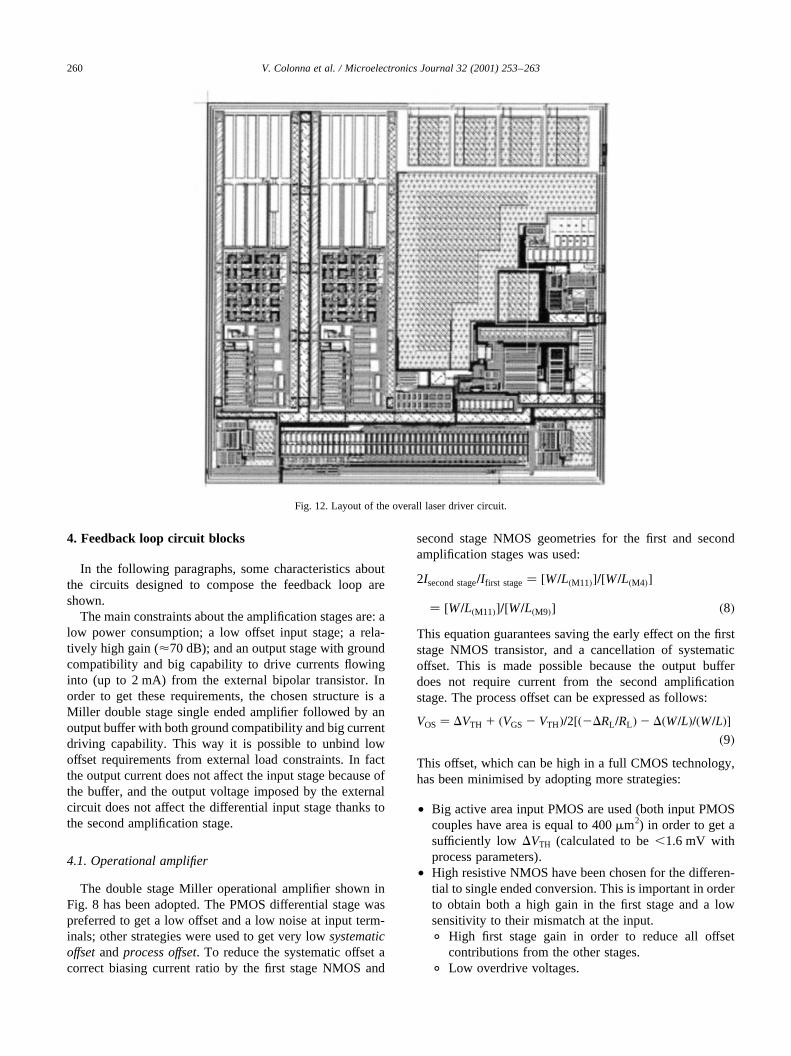
The system has been designed in a 0.35mm standardCMOS technology to be embedded in a single-chip front-end. The circuit layout is shown in Fig. 12. The chip area isabout 0.3 mm2. The overall power consumption is about9 mW (6mW in stand by mode).
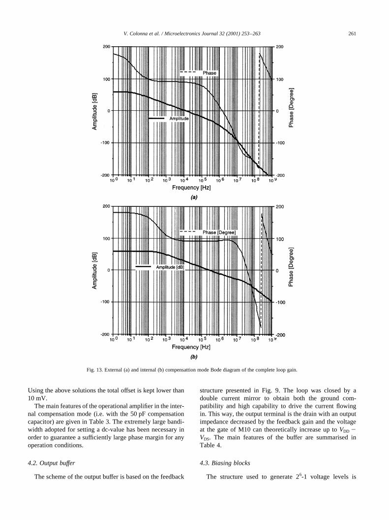
Fig. 13 shows the frequency response of the completefeedback loop structure, including the external componentsand pick-up, for the external compensation mode and theinternal compensation mode, respectively. About the pick-up, a typical gainRLD � 9 dBV was considered and,according to the discussion proposed for the loop gainchoosing, the high gain value (74 dB) was set.
As can be seen, the bandwidth is<10 kHz in the first case(a) and <200 kHz in the second case (b), whereas thecomplete feedback loop DC gain (GLOOP) is 58 dB forboth configurations. It is important to note how the stabilityis ensured even if the pick-up gain rises up to 21 dBV (themaximum gain value considered for this gain choice): in this
V. Colonna et al. / Microelectronics Journal 32 (2001) 253–263262
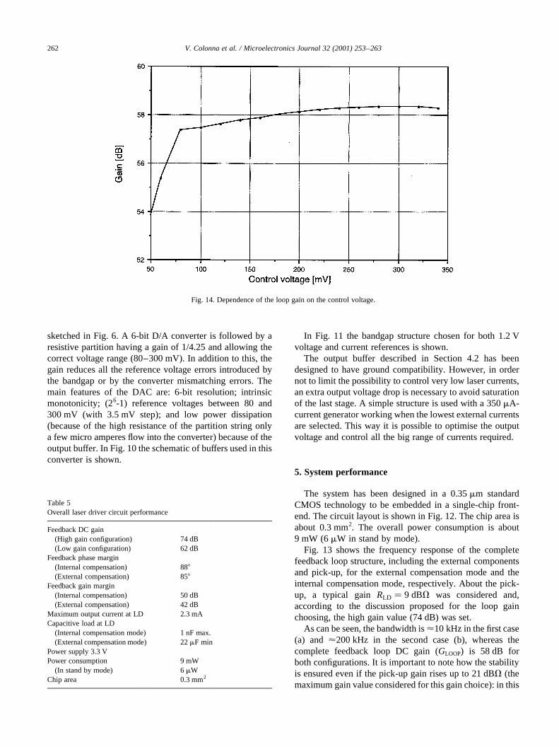
Fig. 14. Dependence of the loop gain on the control voltage.
Table 5Overall laser driver circuit performance
Feedback DC gain(High gain configuration) 74 dB(Low gain configuration) 62 dB
Feedback phase margin(Internal compensation) 888
(External compensation) 858
Feedback gain margin(Internal compensation) 50 dB(External compensation) 42 dB
Maximum output current at LD 2.3 mACapacitive load at LD
(Internal compensation mode) 1 nF max.(External compensation mode) 22mF min
Power supply 3.3 VPower consumption 9 mW
(In stand by mode) 6mWChip area 0.3 mm2
case, the gain bandwidth of the total system is increased byabout half a decade�21 dB2 9 dB� 12 dB� while thephase margin remains higher than 608 and the gain marginremains higher than 30 dB, for both the compensationmodes, as shown in Fig. 13.
Both the programmable gain stages were been simulated inevery condition to guarantee a constant DCgain for every laserdiode current chosen. The output stage is DC coupled with theexternal bipolar and the current coming in from this devicechanges with the current chosen and with theb of this tran-sistor. The output current driving capability, in addition to theground compatibility of the output stage, allow a degradationof the DC gain lower than 1 dB, as shown in Fig. 14.
Worst case model simulations performed for a tempera-ture range of 40–1408C have shown that the DC degradationis lower than 2 dB, without an appreciable changing ofstability performances in terms of phase and gain margin.
The load was also be considered: the system has thepossibility to drive a very high output current (up to2.3 mA) and a capacitive load up to 1 nF with the internalcompensation mode. As already mentioned, with theexternal compensation mode, the minimum capacitorsuggested is 22mF.
Table 5 summarizes the simulated performance of theproposed laser driver.
6. Conclusions
A laser driver circuit to be realized in a standard 0.35mmCMOS technology has been proposed. A considerable
number of techniques have been adopted to improve itsversatility. These techniques mainly regard: a programma-ble gain; a programmable biasing; and the possibility ofusing an internal or an external compensation capacitor.With respect to standard laser driver integrated systemsalready available in the literature and/or in the market, theproposed circuit allows to operate properly with a largenumber of pick-up’s with different electrical characteristicsfor different application areas; this at the cost of a negligibleextra area and power consumption.
The proposed techniques and the design are very robust inorder to make the circuit readily usable in commercialapplications.
References
[1] K.C. Pohlmann, The Compact Disc Handbook, 2nd ed., OxfordUniversity Press, Oxford, 1995.
[2] C. Sherman, CD-ROM Handbook, 2nd ed., Mc Graw-Hill, New York,1994.
[3] F. Dell’Ova, B. Bonhoure, F. Paillardet, Embeddable CMOS 3.3Vanalog front-end for CD applications, IEEE Transactions on ConsumerElectronics August (1995) 821–826.
[4] A. Baschirotto, G. Brasca, V. Colonna, P. Cusinato, G. Gandolfi, S.Stefani, D. Tonietto, A.C.D. analog, front-end in BiCMOS technology,ESSCIRC September (1998) 220–223.
[5] Sony, Optical Disk, Data Book semiconductor, pp. 94–95.[6] Mitsubishi, Optical Semiconductor Devices and Optical-Fiber
Communications Systems, Data Book, 1992.[7] R.J. Van der Plassche, Integrated Analog-to-Digital and Digital-to-
Analog Converters, Kluwer Academic, Dordrecht, 1994.
V. Colonna et al. / Microelectronics Journal 32 (2001) 253–263 263