DESIGN OF RADIATION-HARD CMOS SENSORS FOR ...
135
CERN-THESIS-2019-221 29/10/2019 FACULTY OF ELECTRICAL ENGINEERING AND COMPUTING Ivan Berdalovi´ c DESIGN OF RADIATION-HARD CMOS SENSORS FOR PARTICLE DETECTION APPLICATIONS DOCTORAL THESIS Zagreb, 2019
-
Upload
khangminh22 -
Category
Documents
-
view
3 -
download
0
Transcript of DESIGN OF RADIATION-HARD CMOS SENSORS FOR ...

CER
N-T
HES
IS-2
019-
221
29/1
0/20
19
FACULTY OF ELECTRICAL ENGINEERING AND COMPUTING
Ivan Berdalovic
DESIGN OF RADIATION-HARD CMOSSENSORS FOR PARTICLE DETECTION
APPLICATIONS
DOCTORAL THESIS
Zagreb, 2019

FACULTY OF ELECTRICAL ENGINEERING AND COMPUTING
Ivan Berdalovic
DESIGN OF RADIATION-HARD CMOSSENSORS FOR PARTICLE DETECTION
APPLICATIONS
DOCTORAL THESIS
Supervisor: Professor Tomislav Suligoj, PhD
Zagreb, 2019

FAKULTET ELEKTROTEHNIKE I RACUNARSTVA
Ivan Berdalovic
PROJEKTIRANJE CMOS SENZORAOTPORNIH NA ZRACENJE ZA
PRIMJENU U DETEKCIJI CESTICA
DOKTORSKI RAD
Mentor: Prof. dr. sc. Tomislav Suligoj
Zagreb, 2019.

The doctoral thesis was done at the University of Zagreb, Faculty of Electrical Engineer-
ing and Computing, at the Department of electronics, microelectronics, computer and
intelligent systems.
Supervisor: Professor Tomislav Suligoj, PhD
The doctoral thesis contains: 120 pages
Doctoral thesis no.:

About the Supervisor
Tomislav Suligoj received his Engineer Diploma, MSc and PhD degrees in electrical engineer-
ing from the University of Zagreb, Faculty of Electrical Engineering and Computing (FER),
Croatia, in 1995, 1998 and 2001, respectively. Currently, he is a full professor at FER, Depart-
ment of Electronics, Microelectronics, Computer and Intelligent Systems, teaching the courses
in the area of electronics and microelectronics. He was a visiting researcher at the University
of California, Los Angeles (1999-2001) and a postdoctoral researcher at the Hong Kong Uni-
versity of Science and Technology (2001-2002). He has been a Principal Investigator of more
than 20 projects so far, supported by government agencies, international companies and uni-
versities. He has published 19 patents and more than 140 papers in journals and conference
proceedings in the area of design, measurements and modelling of electron devices, micro- and
nano- electronics, semiconductor technology and integrated circuit design. Prof. Suligoj has re-
ceived 14 scientific awards including the National Science Award in 2015; the Golden plaque at
the innovation exhibition ARCA; Best paper awards at the MIPRO MEET conference, Faculty
medals "Josip Loncar" for outstanding Doctoral Dissertation, and a Fulbright scholarship. He is
a Technical Program Committee member and a Chairman of Device Physics Subcommittee at
IEEE Bipolar/BiCMOS Circuits and Technology Meeting (BCTM). He is a Steering Committee
member of the MIPRO MEET conference. He was the President of the Electron Devices/Solid-
State Circuits Joint Chapter, IEEE Croatia Section from 2010 until 2013. He gave numerous
invited talks at conferences, universities, institutions and companies.

O mentoru
Tomislav Suligoj je diplomirao, magistrirao i doktorirao u polju elektrotehnike na Sveucilištu
u Zagrebu, Fakultetu elektrotehnike i racunarstva (FER), 1995., 1998. odnosno 2001. go-
dine. Trenutno je redoviti profesor na Zavodu za elektroniku, mikroelektroniku, racunalne i
inteligentne sustave FER-a, gdje predaje kolegije u podrucju elektronike i mikroelektronike.
Bio je gostujuci istraživac na University of California, Los Angeles od 1999. do 2001. godine
te na poslijedoktorskom usavršavanju na Hong Kong University of Science and Technology
od 2001. do 2002. Do sada je vodio više od 20 projekata financiranih od strane državnih in-
stitucija, medunarodnih kompanija i sveucilišta. Objavio je 19 patenata i više od 140 radova u
casopisima i zbornicima konferencija u podrucju projektiranja, mjerenja i modeliranja elektron-
ickih elemenata, mikro- i nano- elektronike, poluvodicke tehnologije i projektiranja integriranih
sklopova. Prof. Suligoj dobitnik je 14 nagrada ukljucujuci Državnu nagradu za znanost 2015.
g., Zlatnu plaketu na izložbi inovacija ARCA, Best paper award na MIPRO MEET konferen-
ciji, srebrnu plaketu "Josip Loncar" za posebno istaknutu doktorsku disertaciju te Fulbrightovu
stipendiju. Clan je Technical Program Committee i Chairman of Device Physics Subcommit-
tee konferencije IEEE Bipolar/BiCMOS Circuits and Technology Meeting (BCTM). Clan je
Steering Committee konferencije MIPRO MEET. Bio je predsjednik Odjela za elektronicke el-
emente i poluvodicke integrirane sklopove Hrvatske sekcije IEEE 2010.-2013. Održao je velik
broj pozvanih predavanja na medunarodnim konferencijama, sveucilištima, institutima i kom-
panijama.

Acknowledgement
I would like to thank my supervisors at CERN, Dr. Heinz Pernegger and Dr. Walter Snoeys
for their help and guidance throughout this PhD project. Working with you has been an honour
and an experience I will never forget. I would also like to thank my supervisor at the University
of Zagreb, Prof. Tomislav Suligoj for his support during the PhD and for letting me pursue the
topics I was interested in, never pressuring me to do anything that was not in my best interest.
Thanks to Thanushan Kugathasan, Cesar Augusto Marin Tobon, Enrico Junior Schioppa, Car-
los Solans Sanchez and everyone else in the EP-ESE-ME and EP-ADE-ID groups who made
this work possible. Special thanks to Valerio Dao, whose firmware and software expertise are
responsible for a lot of the fancy plots included in this thesis. Thanks also to my office mates,
Roberto Cardella, Francesco Piro and Leyre Flores for endless discussions on everything re-
lated to electronics and physics, especially during philosophical Fridays. Finally, thanks to my
family, who have supported me every step of the way, even from a thousand kilometres away.
You continue to provide inspiration and motivation for everything I want to do in life.
This research project has been supported by a Marie Skłodowska-Curie Innovative Training
Network Fellowship of the European Commission’s Horizon 2020 Programme under contract
number 675587 STREAM.

Abstract
The work focuses on the design of large-scale radiation-hard monolithic CMOS sensors for
the upgrades of the detectors in the high-energy physics experiments at CERN. The sensors are
manufactured using a novel process modification implemented in the TowerJazz 180 nm CMOS
process, which uses small collection electrodes to achieve a low sensor capacitance in the order
of a few femtofarads, resulting in low noise and low analogue power consumption. The process
modification provides full depletion of the sensitive layer and a radiation hardness promising
to meet the requirements of the pixel detectors in CERN’s largest experiments. The sensors
implement a matrix of small pixels (in the order of 30 micrometres) containing a fast, low-noise
front-end amplifier and a novel asynchronous digital readout architecture. Measurement results
from these sensors before and after irradiation are also discussed.
Keywords: Active pixel sensors, CMOS integrated circuits, position sensitive particle de-
tectors, radiation effects, radiation hardening (electronics), semiconductor detectors, solid-state
circuit design

Projektiranje CMOS senzora otpornih na zracenje za prim-
jenu u detekciji cestica
Potraga za novim otkricima u fizici cestica u Velikom hadronskom sudaracu (engl. Large
Hadron Collider, LHC) u Europskoj organizaciji za nuklearna istraživanja (CERN) temelji se
na detekciji cestica nastalih u sudarima protona ili teških iona. Protoni se kroz kompleks akcel-
eratora ubrzavaju do energija od 6.5 TeV te se sudaraju u cetiri najveca eksperimenta: ATLAS,
CMS, ALICE i LHCb. Eksperimenti se sastoje od slojeva detektora koji su postavljeni u kon-
centricnim cilindrima oko tocke sudara te služe za mjerenje naboja, kolicine gibanja i energije
cestica nastalih u sudarima kao i cestica nastalih raspadom kratkoživucih cestica. U slucaju
eksperimenta ATLAS, detektori se mogu podijeliti na nekoliko glavnih vrsta. Unutrašnji detek-
tor (engl. Inner Detector, ID) sastoji se od silicijskih piksel i strip detektora visoke rezolucije
položaja koji služe za precizno pracenje cestica blizu mjesta sudara. Pomocu njih se obavlja
rekonstrukcija putanja cestica u magnetskom polju, gdje zakrivljenost putanje otkriva naboj i
kolicinu gibanja cestica. Elektromagnetski i hadronski kalorimetri služe za mjerenje energije
cestica, dok mionski spektrometar obavlja mjerenje kolicine gibanja miona koji produ kroz sve
ostale slojeve eksperimenta.
Buduci da su zanimljivi fizikalni procesi (poput raspada Higgsova bozona) vrlo rijetki, LHC
ce izmedu 2023. i 2025. biti podvrgnut nadogradnji koja ce povecati broj sudara cestica u je-
dinici vremena za gotovo red velicine. Kako bi se mogli nositi s ovakvim porastom luminoziteta,
nekolicinu sustava, ukljucujuci i detektore, takoder ce biti potrebno nadograditi. Veci broj ces-
tica rezultirat ce vecim brojem detekcija u jedinici vremena, što bi moglo dovesti do smanjenja
efikasnosti zbog ogranicenja u brzini ocitavanja podataka iz detektora. Dodatno ogranicenje, os-
obito kod piksel detektora blizu mjesta sudara, su oštecenja uzrokovana ekstremnim kolicinama
zracenja u tim sredinama tijekom citavog vremena života detektora. Trenutno svi eksperimenti
koriste tzv. hibridne piksel detektore za pracenje cestica u unutrašnjim slojevima. Kod ovakve
vrste detektora, sam senzor je proizveden na zasebnoj plocici silicija, dok je elektronika za oci-
tavanje proizvedena na drugoj plocici, obicno u standardnom CMOS procesu, te je sa senzorom
povezana malim vodljivim spojevima (engl. flip-chip bump-bonding). Senzor je zasebno op-
timiran za rad u uvjetima visoke razine zracenja, dok sklopovlje za ocitavanje projektirano u
tehnologiji malih dimenzija omogucuje visoku brzinu i sofisticirano procesiranje podataka.
Iako su zbog dobrih performansi hibridni detektori trenutno standard u detekciji cestica,
jedan od glavnih nedostataka jest komplicirana i skupa tehnologija povezivanja dva cipa. Osim
toga, disipacija snage i samim time zahtjevi za hladenjem detektora su visoki, što rezultira ve-
likom kolicinom materijala, koja pak ogranicava rezoluciju kolicine gibanja zbog raspršenja
cestica u materijalu. Zbog toga u novije vrijeme dolazi do razvoja monolitnih CMOS aktivnih
piksel senzora (engl. CMOS monolithic active pixel sensors, MAPS), kod kojih su senzor

i sklopovlje za ocitavanje integrirani unutar jedne plocice silicija. To u potpunosti eliminira
potrebu za povezivanjem cipova, što uz korištenje komercijalnih CMOS procesa znaci da su
cjenovno vrlo povoljni. Osim toga, kod ovih se detektora kapacitet senzora može dovesti do
ekstremno niskih razina, što rezultira niskom potrošnjom snage u odnosu na hibridne detektore
te smanjenjem kolicine materijala. Do nedavno, glavni nedostatak ove tehnologije bila je nedo-
voljna otpornost na zracenje. Medutim, razvojem CMOS senzorskih procesa, kao što je opisano
i u ovom radu, dolazi do pojave monolitnih senzora s poboljšanom otpornošcu na zracenje, što
ih cini kandidatima cak i za najzahtjevnije primjene. Monolitni CMOS senzori u ovom radu
projektirani su s ciljem zadovoljavanja zahtjeva za vanjske slojeve piksel detektora u eksperi-
mentu ATLAS nakon nadogradnje LHC-a. Neki od najvažnijih zahtjeva su efikasnost detekecije
od preko 97%, vremenska rezolucija od 25 ns, koliko iznosi vrijeme izmedu sudara dva snopa
protona, i to uz potrošnju snage ispod 500 mW/cm2. Zahtjevi moraju biti zadovoljeni nakon
što su detektori podvrgnuti dozi od 1015 1 MeV neq/cm2 neionizirajuceg zracenja te 50 Mrad
ioniziruceg zracenja tijekom citavog vremena života u eksperimentu.
Osnovni mehanizam za detekciju cestica u siliciju jest stvaranje parova elektron-šupljina u
zaporno polariziranom p-n spoju. Broj ioniziranih nosilaca ovisi o gubitku energije cestice koja
prolazi kroz materijal, a koji ovisi o vrsti i samoj energiji cestice. Jedan tip ioniziranih nosi-
laca sakuplja se na jednoj elektrodi p-n spoja. Naboj generiran unutar osiromašenog podrucja
brzo se sakuplja driftom, a ako senzor nije potpuno osiromašen, i difuzija iz kvazineutralnih
podrucja sudjeluje u procesu sakupljanja naboja. Osim ionizacije parova elektron-šupljina, vi-
sokoenergetske cestice mogu izbiti jezgre silicija iz položaja u kristalnoj rešetci, što dovodi
do stvaranja defekata u kristalu. To rezultira pojavom energetskih nivoa unutar zabranjenog
pojasa (tzv. zamki) koji mogu zarobiti ionizirane nosioce naboja i dovesti do gubitka signala.
Kako vjerojatnost zarobljavanja nosilaca ovisi o vremenu sakupljanja naboja, glavna strategija
za postizanje otpornosti na ovo neionizirajuce zracenje (engl. non-ionising energy loss, NIEL)
jest sakupljati naboj driftom i tako smanjiti vrijeme sakupljanja i vjerojatnost zarobljavanja.
Dva su glavna pristupa u izvedbi sakupljacke elektrode u monolitnim piksel detektorima, i
to izvedba s malom sakupljackom elektrodom, gdje elektroda zauzima tek mali dio piksela, a
elektronika za ocitavanje nalazi se odvojeno od elektrode, te izvedba s velikom sakupljackom
elektrodom, gdje elektroda zauzima vecinu površine piksela, a sklopovlje je smješteno unutar
elektrode. Prednost male elektrode je izuzetno nizak kapacitet senzora (reda velicine neko-
liko femtofarada), što je povoljno za razinu šuma i disipaciju snage analognih sklopova koji
slijede. Medutim, nedostatak male elektrode jest cinjenica da je teško postici potpuno osiro-
mašenje sloja za detekciju i samim time zadovoljavajucu otpornost na zracenje. Za potpuno
osiromašenje i sakupljanje driftom stoga je povoljnije koristiti piksele s velikom elektrodom,
koja medutim znaci znatno veci ulazni kapacitet i vece preslušavanje iz digitalnih sklopova za
ocitavanje prema sakupljackoj elektrodi.

Kako su sakupljeni naboji relativno mali (reda velicine nekoliko femtokulona), signale s
elektrode potrebno je pojacati, što se standardno radi pojacalom osjetljivim na naboj s kapaci-
tivnom povratnom vezom unutar piksela. Važno je da pojacalo ima visoko pojacanje te nizak
šum, uz visoku brzinu odziva. Nakon pojacala obicno slijedi filtar za suzbijanje nisko- i vi-
sokofrekventnih komponenti šuma te komparator, koji osigurava da se ocitavaju samo signali
iznad odredenog praga detekcije. Digitalna arhitektura za ocitavanje koja slijedi nakon kom-
paratora vrši dodatno procesiranje signala komparatora te mora do izlaza cipa dovesti tocnu
adresu piksela unutar dvodimenzionalne matrice u kojima je obavljena detekcija, a u nekim
primjenama i informaciju o amplitudi detektiranog signala.
Treba napomenuti da zracenje utjece i na sklopovlje za pojacanje i ocitavanje. U ovom
slucaju, ionizirajuce zracenje (engl. total ionising dose, TID) uzrokuje nakupljanje pozitivnog
naboja u silicijevom dioksidu upravljacke elektrode ili u izolacijskom oksidu tranzistora. Naboj
na upravljackoj elektrodi dovodi do promjena u naponu praga tranzistora, dok naboj u izo-
lacijskom oksidu može dovesti do porasta struje curenja izmedu uvoda i odvoda NMOS tranzis-
tora. Ovi se efekti najcešce sprjecavaju primjenom tranzistora s kružnom upravljackom elek-
trodom (engl. enclosed layout transistors, ELT), cime se osigurava da sva struja tece ispod
upravljacke elektrode.
Monolitni CMOS senzori projektirani u ovom radu proizvedeni su u TowerJazz 180 nm
CMOS procesu. Ova tehnologija koristi male sakupljacke elektrode n-tipa. Sklopovlje je odvo-
jeno od elektrode i zašticeno dubokom implantacijom p-tipa kako podloga PMOS tranzistora
ne bi sudjelovala u sakupljanju signalnog naboja. Epitaksijalni sloj p-tipa debljine 25-30 µm
koristi se kao sloj za detekciju. Visoka otpornost tog sloja pomaže osiromašenju oko sakupl-
jacke elektrode, no da bi se postiglo potpuno osiromašenje epitaksijalnog sloja i zadovoljavajuca
otpornost na neionizirajuce zracenje, potrebna je modifikacija procesa dodavanjem niskodopi-
ranog sloja n-tipa preko cijele matrice piksela. Nakon dobrih rezultata na prototipima senzora
u ovom modificiranom procesu, zapocinje projektiranje velikih detektora koji bi zadovoljili
specifikacije eksperimenta ATLAS.
MALTA (engl. Monolithic from ALICE To ATLAS) je senzor koji sadrži matricu od
512×512 piksela velicine 36.4×36.4 µm2. Svaki piksel osim male sakupljacke elektrode prom-
jera 2-3 µm sadrži analogni dio sklopovlja, koji se sastoji od ulaznog pojacala i komparatora, te
digitalnu logiku za ocitavanje adrese piksela. Ulazno pojacalo temelji se na uvodskom sljedilu
koje sakupljeni naboj prenosi s velikog kapaciteta na mali parazitni kapacitet, pri cemu dolazi do
visokog naponskog pojacanja. Vrijeme odziva ovisi o sakupljenom naboju, a jedan od glavnih
zahtjeva je osigurati dovoljno kratko vrijeme odziva kako bi se svaka detekcija mogla obaviti
unutar 25 ns, što je ovom topologijom moguce postici uz disipaciju snage manju od 1 µW po
pikselu. Pojacalo je optimirano za prag detekcije od 200 e−, a pri tome u tranzijentnim simu-
lacijama šuma pokazuje ukupni ekvivalentni šum na ulazu od tek 7 e−. Dimenzije tranzistora

optimirane su i na nacin da procesne varijacije što manje utjecu na rasipanje praga detekcije, te
Monte Carlo simulacije pokazuju standardnu devijaciju praga detekcije od samo 8 e−. Struje
i naponi potrebni za rad pojacala generiraju se pomocu digitalno-analognih pretvornika, a kri-
ticni tranzistori u pojacalu i pretvornicima izvedeni su u topologiji s kružnom upravljackom
elektrodom radi otpornosti na ionizirajuce zracenje.
Digitalna elektronika za ocitavanje koristi novi, asinkroni nacin prijenosa podataka unutar
matrice piksela. Digitalni impulsi na izlazu komparatora koriste se u generiranju 22-bitnog
uzorka kratkih impulsa trajanja do 2 ns, koji se asinkrono šalje niz stupac piksela i sadrži kodi-
ranu adresu piksela u kojem je obavljena detekcija unutar stupca. Prednost asinkronog pris-
tupa je cinjenica da nema signala takta unutar velike matrice, što znacajno smanjuje digitalnu
potrošnju snage, a pritom omogucuje veci broj detekcija u jedinici vremena. Na periferiji cipa,
signali iz svih stupaca spajaju se u jednu rijec od 40 bita, koja jednoznacno odreduje adresu
piksela unutar matrice, te se rijec sa izlaza cipa LVDS standardom šalje do vanjskih sustava za
pohranu podataka. Zbog asinkronog prijenosa potrebno je voditi racuna o tome da svi signali
unutar rijeci stignu do izlaza cipa u isto vrijeme, što znaci da kapaciteti linija svih bitova u
cijelom lancu prijenosa moraju biti potpuno izjednaceni.
Proizvedeni MALTA senzori okarakterizirani su u laboratoriju i u testiranjima zrakom ces-
tica. Pokazuje se da su analogni ulazni sklopovi potpuno funkcionalni te da vremenski odziv
odgovara simuliranim vrijednostima. Uz dovoljno nizak prag detekcije, preko 98% signala de-
tektira se unutar 25 ns, cak i bez korekcije za trajanje propagacije impulsa niz stupac piksela od
8 ns. Srednja vrijednost ekvivalentnog šuma ulaznog pojacala takoder odgovara simulacijama,
no primjeceno je da raspodjela šuma ne odgovara Gaussovoj raspodjeli, što se dovodi u vezu
s malim dimenzijama pojedinih tranzistora u pojacalu i time uzrokovanog porasta šuma (engl.
random telegraph signal noise, RTS) u pojedinim pikselima. Osim toga, rasipanje praga detek-
cije unutar matrice je znatno vece od simuliranih vrijednosti, što u kombinaciji s RTS šumom
ogranicava prag detekcije na iznad 200 e−. U testiranjima zrakom cestica zakljucuje se da uz
najniže moguce pragove detekcije senzor prije zracenja postiže visoku efikasnost detekcije od
preko 97%, uniformnu po cijeloj površini piksela.
Nakon ozracenja neutronima do 1015 neq/cm2 i x-zrakama do 70 Mrad, analogni i digi-
talni sklopovi su i dalje funkcionalni, uz nešto veci šum i rasipanje praga detekcije. Pojacanje
ulaznog sklopa ne razlikuje se od onog prije zracenja zahvaljujuci topologiji otpornoj na ion-
izirajuce zracenje. Medutim, testiranja zrakom cestica pokazuju znatan pad efikasnosti detekcije
pri rubovima piksela, daleko od sakupljacke elektrode. Iako je senzor u modificiranom procesu
potpuno osiromašen, gubitak efikasnosti povezan je s manjkom lateralnog elektricnog polja pri
rubovima piksela, što dovodi do zarobljavanja nosilaca u zamkama uzrokovanim neionizira-
jucim zracenjem i do gubitka signala. Zbog toga maksimalna srednja efikasnost unutar piksela
uz najniže dostižne pragove detekcije iznosi tek oko 80%.

Kako bi se poboljšala efikasnost detekcije nakon zracenja, pomocu TCAD simulacija razvi-
jene su nove procesne promjene s ciljem povecanja lateralnog elektricnog polja. Pokazuje se
da se uvodenjem dodatne duboke implantacije p-tipa ili uvodenjem razmaka u postojecu im-
plantaciju n-tipa pri rubovima piksela elektricno polje te samim time nosioci bolje usmjeravaju
prema sakupljackoj elektrodi, te da je ukupni sakupljeni naboj nakon zracenja znatno veci. Zbog
toga zapocinje projektiranje nove, manje verzije MALTA cipa s ovim procesnim promjenama,
nazvane miniMALTA. Osim procesnih promjena, unutar matrice piksela povecane su dimenzije
kriticnih tranzistora kako bi se suzbio RTS šum i dobilo vece pojacanje. Na periferiji cipa pro-
jektirana je i nova generacija digitalnog sklopovlja za ocitavanje, koja sinkronizira asinkrone
signale iz matrice i olakšava daljnje procesiranje podataka, zadržavajuci pritom nisku digitalnu
potrošnju snage. Sklop za sinkronizaciju temelji se na polju RAM memorijskih celija u koje se
pohranjuje informacija o adresi piksela i vremenu detekcije. RAM memorija se zatim sinkrono
ocitava te se informacija sinkrono šalje s cipa.
Prvi rezultati mjerenja na ulaznom pojacalu novog miniMALTA cipa pokazuju znatno vece
pojacanje zbog veceg izlaznog otpora na izlaznom cvoru pojacala, što znaci da se uz iste
postavke pojacala mogu postici niži pragovi detekcije. Osim toga, povecanje dimenzija tranzis-
tora gotovo u potpunosti eliminira RTS šum cak i nakon ozracenja, što ponovno znaci da je lakše
postici niže pragove. Sklopovlje za sinkronizaciju takoder se pokazalo potpuno funkcionalnim
te je moguce ocitati tocnu adresnu i vremensku informaciju pri svakoj detekciji. U testiranjima
zrakom cestica prije zracenja, sektori cipa u kojima su implementirane procesne promjene uz
niski prag detekcije od ispod 200 e− pokazuju efikasnost od preko 99%. Nakon ozracenja do
1015 neq/cm2, efikasnost u tim sektorima još uvijek iznosi oko 98%, što znaci da povecanje lat-
eralnog elektricnog polja uz niski prag detekcije dovodi to gotovo potpune efikasnosti detekcije
cak i nakon zahtijevanih doza zracenja.
Nakon ovih rezultata, nastavlja se projektiranje sljedecih verzija velikih detektora u Tower-
Jazz 180 nm tehnologiji. Dodatna poboljšanja ulaznih sklopova omogucit ce još vece pojacanje
i niži prag detekcije, a unutar svakog piksela dodano je i sklopovlje za podešavanje praga detek-
cije, cime ce se smanjiti rasipanje praga unutar velike matrice. Uz smanjenje dimenzija piksela
na oko 33 µm, to bi trebalo dovesti do još više efikasnosti i još bolje otpornosti na zracenje.
Poboljšanja ce biti ukljucena u dva velika detektora s razlicitim vrstama digitalnih sklopova za
ocitavanje, koji ce biti poslani na proizvodnju krajem 2019.
Kljucne rijeci: Aktivni piksel senzori, CMOS integrirani sklopovi, detektori cestica os-
jetljivi na položaj, efekti zracenja, otpornost (elektronike) na zracenje, poluvodicki detektori,
projektiranje poluvodickih sklopova

Contents
1. Introduction . . . . . . . . . . . . . . . . . . . . . . . . . . . . . . . . . . . . . . 1
1.1. Detectors in the high-energy physics experiments at CERN . . . . . . . . . . . 1
1.2. Pixel detectors for the LHC High-Luminosity upgrade . . . . . . . . . . . . . 6
2. CMOS monolithic active pixel sensors . . . . . . . . . . . . . . . . . . . . . . . . 10
2.1. Detection of particles in silicon . . . . . . . . . . . . . . . . . . . . . . . . . . 10
2.1.1. Energy loss of charged particles . . . . . . . . . . . . . . . . . . . . . 10
2.1.2. Signal formation in the sensor . . . . . . . . . . . . . . . . . . . . . . 13
2.2. Radiation effects in the sensor – Non-ionising energy loss . . . . . . . . . . . . 16
2.3. Monolithic sensor concepts . . . . . . . . . . . . . . . . . . . . . . . . . . . . 19
2.3.1. Small collection electrode designs . . . . . . . . . . . . . . . . . . . . 19
2.3.2. Large collection electrode designs . . . . . . . . . . . . . . . . . . . . 21
2.3.3. Other approaches - DEPFET and SOI . . . . . . . . . . . . . . . . . . 22
2.4. Radiation effects in the electronics – Total ionising dose and single event effects 22
2.5. Front-end and readout concepts . . . . . . . . . . . . . . . . . . . . . . . . . . 25
3. Design and characterisation of radiation-hard CMOS sensors . . . . . . . . . . . 30
3.1. Sensor technology . . . . . . . . . . . . . . . . . . . . . . . . . . . . . . . . . 30
3.1.1. The standard TowerJazz 180 nm process . . . . . . . . . . . . . . . . . 30
3.1.2. Designs in the modified TowerJazz process . . . . . . . . . . . . . . . 31
3.2. Analogue front-end circuit . . . . . . . . . . . . . . . . . . . . . . . . . . . . 36
3.2.1. Principle of operation . . . . . . . . . . . . . . . . . . . . . . . . . . . 36
3.2.2. Timing optimisation . . . . . . . . . . . . . . . . . . . . . . . . . . . 40
3.2.3. Noise and mismatch . . . . . . . . . . . . . . . . . . . . . . . . . . . 43
3.2.4. Considerations for radiation hardness . . . . . . . . . . . . . . . . . . 46
3.2.5. Bias generation using digital-to-analogue converters . . . . . . . . . . 46
3.3. Digital readout electronics . . . . . . . . . . . . . . . . . . . . . . . . . . . . 49
3.3.1. Asynchronous matrix readout . . . . . . . . . . . . . . . . . . . . . . 49
3.3.2. End-of-column readout logic . . . . . . . . . . . . . . . . . . . . . . . 54

3.4. Sensor characterisation before irradiation . . . . . . . . . . . . . . . . . . . . 57
3.4.1. Sensor and analogue performance in lab tests . . . . . . . . . . . . . . 57
3.4.2. Measurements on readout architecture . . . . . . . . . . . . . . . . . . 62
3.4.3. Beam test results . . . . . . . . . . . . . . . . . . . . . . . . . . . . . 68
3.5. Performance of irradiated sensors . . . . . . . . . . . . . . . . . . . . . . . . 70
3.5.1. Sensor and front-end after irradiation . . . . . . . . . . . . . . . . . . 70
3.5.2. Efficiency in beam tests . . . . . . . . . . . . . . . . . . . . . . . . . 74
4. Optimisation of pixel matrix and readout electronics . . . . . . . . . . . . . . . . 78
4.1. Process improvements for radiation hardness . . . . . . . . . . . . . . . . . . 78
4.2. Pixel matrix design changes . . . . . . . . . . . . . . . . . . . . . . . . . . . 80
4.3. Synchronisation at the end-of-column . . . . . . . . . . . . . . . . . . . . . . 81
4.3.1. Random-access memory for synchronisation . . . . . . . . . . . . . . 81
4.3.2. Peripheral readout logic . . . . . . . . . . . . . . . . . . . . . . . . . 83
4.4. Test results before and after irradiation . . . . . . . . . . . . . . . . . . . . . . 85
5. Outlook for future design improvements . . . . . . . . . . . . . . . . . . . . . . . 100
5.1. Further optimisation of analogue front-end circuitry . . . . . . . . . . . . . . . 100
5.2. In-pixel threshold tuning . . . . . . . . . . . . . . . . . . . . . . . . . . . . . 103
6. Conclusion . . . . . . . . . . . . . . . . . . . . . . . . . . . . . . . . . . . . . . . 107
Bibliography . . . . . . . . . . . . . . . . . . . . . . . . . . . . . . . . . . . . . . . . 109
Biography . . . . . . . . . . . . . . . . . . . . . . . . . . . . . . . . . . . . . . . . . . 117
Životopis . . . . . . . . . . . . . . . . . . . . . . . . . . . . . . . . . . . . . . . . . . 120

Chapter 1
Introduction
1.1 Detectors in the high-energy physics experiments at CERN
The search for new physics at the Large Hadron Collider (LHC) at the European Organisation
for Nuclear Research (CERN) relies on the detection of particles created in proton-proton and
heavy ion collisions. Protons in two counter-rotating beams are accelerated through a complex
of accelerators, shown in fig. 1.1 [1], reaching a beam energy of up to 6.5 TeV in the largest
collider ring, the 27 km circumference LHC. Protons are produced by ionising hydrogen gas
with an electric field. The kinetic energy of the protons is increased from about 100 keV up
to 1.4 GeV in a linear accelerator (LINAC) using radio-frequency cavities and the Proton Syn-
chrotron Booster (PSB) before being injected into the Proton Synchrotron (PS). The PS and the
SPS (Super Proton Synchrotron) accelerate the protons to 25 GeV and 450 GeV, respectively,
before the beams are finally injected into the LHC for further acceleration, from 450 GeV to
6.5 TeV per beam.
Superconducting magnets cooled to temperatures below 2 K and operating at magnetic field
strengths above 8 T are used to bend the particles in the beam around the circular collider. The
beams collide at four crossing points around which the four largest experiments, ATLAS [2],
CMS [3], ALICE [4] and LHCb [5] are positioned. The number of events per second generated
in the LHC collisions is given by:
N = Lσ , (1.1)
where σ is the cross-section for the event in question and L is the machine luminosity. L is
defined only by the beam parameters and can be written as:
L =N2
b nb frevγr
4πεnβ∗F, (1.2)
where Nb is the number of particles per bunch, nb the number of bunches per beam, frev the
1

Introduction
Figure 1.1: An overview of the accelerator complex at CERN and the experiments within it (reproducedfrom [1]).
revolution frequency, γr the relativistic gamma factor, εn the normalised transverse beam emit-
tance, b∗ the beta function at the collision point, and F the geometric luminosity reduction
factor due to the crossing angle at the interaction point [6]. Since the interesting physics events
(such as decays of the elusive Higgs boson) are very rare, the study and exploration of these
events in the LHC collisions requires both high beam energies and high beam intensities. The
two largest general-purpose experiments, ATLAS and CMS, operate with a peak luminosity of
about L = 1034 cm−2s−1 for proton collisions, while the one dedicated ion experiment, ALICE,
aims at a peak luminosity of L = 1027 cm−2s−1 for nominal lead-lead ion operation. Rather
than having continuous beams, the protons are bunched together so that interactions between
the two beams take place at discrete intervals, 25 ns apart, providing a bunch collision rate of
40 MHz. The particles created in these collisions as well as the decay products of particles
with a short lifetime pass through a variety of detectors within the experiments, which provide
information about the charge, momentum and energy of the created particles.
An overview of the detector systems will be given through the example of the ATLAS
experiment, illustrated in fig. 1.2. The experiment consists of a series of detectors placed
in concentric cylinders around the interaction point where the proton beams from the LHC
collide. It can be divided into four major parts: the Inner Detector, the calorimeters, the Muon
2

Introduction
Spectrometer and the magnet systems [7]. The two large superconducting magnet systems are
used to bend charged particles so that their momenta can be measured. The inner solenoid
magnet produces a uniform 2 T magnetic field surrounding the Inner Detector, while the outer
toroidal magnetic field surrounds the calorimeters and the muon system.
Figure 1.2: A cut-away view of the ATLAS experiment and its sub-parts (reproduced from [2]).
The Inner Detector itself consists of high-resolution semiconductor pixel and strip detectors
in the inner part of the tracking volume, as well as straw-tube tracking detectors with the ca-
pability to generate and detect transition radiation in its outer part. The innermost pixel layer
begins about 5 cm from the proton beam axis, and the Inner Detector extends to a radius of 1.2
metres as well as 6.2 metres in length along the beam pipe. Its basic function is to track charged
particles by detecting their interaction with material at discrete points. The curvature of the par-
ticles’ track due to the magnetic field present reveals the charge and momentum of the particles.
Apart from track reconstruction, the precision tracking detectors, i.e. the pixels and semicon-
ductor trackers (SCT), need to be able to reconstruct the interaction point of the particles from
the beam (primary vertices) as well as the decay points of short-lived particles (secondary ver-
tices) with a high resolution. This is achieved by a high granularity in the two-dimensionally
segmented silicon pixel detectors used around the vertex region. The high granularity in the
order 100 µm over such a large area means that the number of readout channels in the Pixel
Detector itself is very high, over 80 million, which is about 50% of the total readout channels
of the whole experiment. The total of nearly 1750 pixel modules are arranged in three layers
around the beam axis in the barrel region and on three disks perpendicular to the beam axis
in the end-cap regions. The pixels in the barrel region provide a spatial resolution of around
10 µm in the direction radial to the beam axis and 70 µm in the direction along the beam axis for
the impact parameter, as well as around 50 µm in the radial direction for the reconstruction of
3

Introduction
secondary vertices. The impact parameter is defined as the perpendicular distance of the closest
approach of a reconstructed track to the primary vertex.
The Semiconductor Tracker (SCT) is the middle component of the Inner Detector and has
a similar function to the Pixel Detector, but with long, narrow strips rather than small pixels,
making coverage of a larger area more practical. The SCT is critical for the tracking in the
plane perpendicular to the beam, since it measures particles over a much larger area than the
Pixel Detector, with more sampled points and similar, albeit one-dimensional accuracy. The
total number of readout channels in the SCT is approximately 6.3 million. The Transition Radi-
ation Tracker (TRT) is the outermost component of the Inner Detector and is composed of drift
tubes (straws), each 4 mm in diameter and up to 144 cm long. The TRT only provides informa-
tion about the radial position, for which it has an intrinsic accuracy of 130 µm per straw. Each
straw is filled with gas that becomes ionised when a charged particle passes through, producing
a current pulse in the wire. The pattern of "hit" straws allow the path of the particle to be deter-
mined. Ultra-relativistic charged particles produce transition radiation in the material between
the straws, resulting in a much stronger signals in some straws and allowing the identification of
the lightest charged particles, electrons and positrons. The total number of TRT readout chan-
nels is approximately 351 thousand. The expected transverse momentum resolution obtained
with the complete Inner Detector is [8]:
σpT
pT= 0.03%pT (GeV)+1.2%. (1.3)
The calorimeters are situated outside the solenoidal magnet that surrounds the Inner Detec-
tor. Their purpose is to measure the energy of particles by absorbing it. There are two basic
calorimeter systems: an inner Electromagnetic Calorimeter and an outer Hadronic Calorime-
ter. Both are sampling calorimeters: they absorb energy in high-density metal and periodically
sample the shape of the resulting particle shower, inferring the energy of the original particle
from this measurement. The Electromagnetic (EM) Calorimeter absorbs energy from particles
that interact electromagnetically, and its fine granularity and energy resolution are ideally suited
for precision measurements on electrons and photons. The energy-absorbing materials are lead
and steel, while liquid argon (LAr) is used as the sampling material. The Hadron Calorimeter
absorbs energy from particles that pass through the EM Calorimeter, primarily hadrons. The
main part of this calorimeter is the tile calorimeter placed directly outside the EM calorimeter
envelope. The energy-absorbing material is steel, with scintillating tiles that sample the en-
ergy deposited. The coarser granularity of this part of the calorimeter is sufficient to satisfy the
physics requirements. In the end-cap regions, the end-cap and forward calorimeters made of
liquid argon, copper and tungsten complete the calorimeter system.
The Muon Spectrometer is a large tracking system designed to accurately measure the mo-
mentum of muons, which pass through all the other elements of the detector before reaching the
4

Introduction
muon systems. It is based on the magnetic deflection of muon tracks in the large superconduct-
ing air-core toroid magnets, instrumented with separate high-precision tracking chambers and
triggering chambers with a high time resolution. The precise measurement of the track coor-
dinates in the principal bending direction of the magnetic field is provided by Monitored Drift
Tubes (MDTs) and Cathode Strip Chamber (CSCs). The trigger chambers, made of Resistive
Plate Chambers (RPCs) and Thin Gap Chambers (TGCs) provide bunch-crossing identifica-
tion and measure the muon coordinate in the direction orthogonal to that determined by the
precision-tracking chambers. In the barrel region, tracks are measured in chambers arranged in
three cylindrical layers around the beam axis; in the transition and end-cap regions, the cham-
bers are installed in planes perpendicular to the beam, also in three layers.
The principle of detecting different types of particles in the experiment is reiterated in fig.
1.3. Charged particles are tracked precisely within the Pixel/SCT Detectors and Transition
Radiation Tracker of the Inner Detector and then absorbed in either the Electromagnetic or
the Hadronic Calorimeter for energy measurement. Muons, which pass through all the other
detector systems, are tracked in the Muon Spectrometer. Neutrinos are the only established
stable particles that cannot be detected directly, and their presence is inferred by measuring a
momentum imbalance among detected particles.
Figure 1.3: A cross-section through the various layers of detectors used in the ATLAS experiment.
The other large general-purpose detector, CMS, uses the same principles in particle detec-
tion, and is composed of an all-silicon tracker, an electromagnetic and hadronic calorimeter as
well as a muon system. The principal difference between the two experiments is the magnet
system, where CMS uses a single solenoid to generate the 4 T magnetic field penetrating all the
detector layers.
5

Introduction
1.2 Pixel detectors for the LHC High-Luminosity upgrade
After 2020, the statistical gain in running the accelerator without a significant luminosity in-
crease beyond its design value will become marginal. Therefore, to maintain scientific progress
and to explore its full capacity, the LHC will undergo a major upgrade during the long shut-
down planned between 2023 and 2025 [9]. The timeline of the upgrade plans is shown in fig.
1.4. After 2025, the peak luminosity will be increased to more than 5×1034 cm−2s−1, which is
a factor of 5-7 higher than the current design value. When integrating the luminosity over the
full operation time of the machine, this gives an integrated luminosity value of 3000 fb−1 that
can be reached until 2035. This integrated luminosity is about ten times the expected luminosity
reach of the first twelve years of the LHC lifetime. To cope with such an increase in luminosity,
a number of systems related to the superconducting magnets, cryogenics and beam collimation
will need to be upgraded. A number of detector systems will need to be upgraded as well, since
the increased particle fluxes will result in higher detector occupancies and efficiency losses due
to readout limitations at high hit rates. Another limitation is the increase in radiation damage
over the full lifetime of the detectors, especially in the pixel detectors closest to the particle
interaction points.
Figure 1.4: Timeline of the upgrade plans for the LHC. After the third long shut-down (LS3), themachine will be in the High-Luminosity configuration (reproduced from [9]).
The three-layer pixel system of the ATLAS detector, designed for an instantaneous luminos-
ity of 1034 cm−2s−1, was already upgraded during the long shut-down in 2013-2014 (LS1) to
cope with the gradually increasing luminosity until the LS3 upgrade. In order to retain the ex-
cellent secondary vertex reconstruction efficiency in the presence of high pile-up, a fourth pixel
detector layer, called the Insertable B-Layer (IBL), was installed inside the three-layer pixel de-
tector, about 3.3 cm from the beam line. As a result, the impact parameter resolution improved
by nearly a factor of 2 for low transverse momentum tracks [10]. For the high-luminosity up-
grade during LS3, the Inner Detector will be replaced by an all-silicon Inner Tracker (ITk)
consisting of five layers of pixel and four layers of strip detectors [11].
6

Introduction
Currently, all the experiments at the LHC use hybrid pixel detectors for the tracking of par-
ticles in the innermost layers. In this type of detector, the sensor part is produced on dedicated
sensor grade silicon material, while the separate pixel readout chip is manufactured using a stan-
dard CMOS process. The traversing particle generates a signal in the sensor part, which is read
out by the readout chip attached to the sensor by using the flip-chip bump-bonding technology.
The readout cells are arranged in the same two-dimensional matrix structure of the pixel cells
of the sensor, as shown in fig. 1.5a. A pixel unit cell of the sensor part together with the readout
cell and the connecting solder bump is shown in fig. 1.5b.
(a)
1 Introduction
5
Pixel detectors with cell sizes of order 100 x 100 µm2 or smaller can operate very close to the beam collision point and can cope with the high particle density in the harsh radia-tion environment (above 1015 particles per cm2 per detector lifetime) encountered in these experiments. The success of the pixel technology has been so great that planned future collider experiments all foresee pixel detectors as the instrument of choice nearest to the interaction point. The assets of hybrid pixels are high rate capability and large radiation tolerance while maintaining very good spatial resolution. On the negative side, however, the hybrid pixel technology bears some serious disadvantages: the assembly (bump & flip-chip technology) is a complex process that drive the cost for large area detectors. The easily achievable pixel dimensions are still rather large (~50-100µm range). Due to the high rates the power consumption and hence the needed cooling power is high, resulting in a big material load in large detector structures, at ATLAS and CMS typically 3% of a radiation length per detector layer. This deteriorates momentum and vertex measurement due to multiple Coulomb scattering in the material, in particular at low track momenta, and is a source of secondary particles from interactions in this material.
Figure 1-1 A cross-section through a typical hybrid pixel sensor with fully depleted
silicon planar sensor and readout.
Promises of Monolithic Active Pixels
The next generation R&D of pixel detectors within the context of the LHC and other yet to be decided upgrades as well as for the planned International Linear Collider, must ad-dress the weaknesses of the current approaches and tailor new pixel developments to the needs of the new generation vertex and tracking detectors. For the LHC detectors the most important ones are for outer layers (R > 25 cm): low-cost large area pixel modules,
(b)
Figure 1.5: (a) A cut-away view and (b) one pixel cell of a hybrid pixel detector. The sensor chip isbump-bonded to the readout chip containing the electronics (reproduced from [12] and [13]).
The large signals collected from the sensor chip optimised for a high-radiation environment
combined with the sophisticated analogue and digital functionality provided by the readout chip
designed in technologies with small feature sizes results in a superior signal-to-noise ratio as
well as comprehensive in-pixel signal processing, rendering the hybrid pixel detector principle
the state-of-the-art technology for today’s precision vertex detectors in particle physics [13].
Further advantages of hybrid pixels are high rate capability and large radiation tolerance while
maintaining a very good spatial resolution.
The three layers of the current ATLAS Pixel Detector utilise planar sensors composed of an
array of diodes placed on a low-doped n-type bulk bump-bonded to FE-I3 readout chips [14].
These chips were designed and fabricated in a commercial 250 nm technology and contain a
matrix of 18×160 pixels with a pixel size of 50×400 µm2. Each chip contains 2880 readout
channels with densely packed analogue and digital circuits, and uses radiation tolerant layout
rules. On the other hand, the IBL modules use the FE-I4 readout chip [15], an evolution of the
FE-I3 designed to cope with the high hit rates very close to the interaction point. The chip was
fabricated in the IBM 130 nm technology that allows a high digital design density and radiation
tolerance. The pixel array consists of 80×336 pixels with a size of 50×250 µm2. These are
bump-bonded to planar silicon sensors in one type of modules or 3D silicon sensors in the other
7

Introduction
type. The 3D sensors, where the electrodes fully penetrate the silicon substrate, were included
for the first time in a large-scale collider experiment to provide superior radiation hardness close
to the interaction point.
Despite good performance in the experiments thus far, the hybrid approach does have its
disadvantages. The module assembly using the bumping and flip-chip technology is a complex
process that drives the cost for large area detectors. The pixel pitches that are easily achievable
are still rather large, in the order of 100 µm. Moreover, the power consumption and hence the
needed cooling power is high, resulting in a large material budget for large detector systems.
This deteriorates the momentum and vertex measurement resolution due to the scattering of
particles in the material.
To overcome these drawbacks, the next generation of R&D focuses on the development
of monolithic active pixel sensors (MAPS). These detectors integrate the sensor and the read-
out electronics inside the same silicon die, thus completely avoiding bump-bonding. CMOS
monolithic active pixel sensors can be produced using commercial CMOS processes and can
therefore be very cost effective. Moreover, the extremely low sensor capacitance that can be
achieved with this approach allows lower power consumption compared to their hybrid coun-
terparts, as described in the following chapters, which reduces the material budget and limits
the probability for the particles to be scattered. So far, radiation hardness has been the main dis-
advantage of CMOS MAPS. However, recent developments in CMOS sensor processing, also
detailed later on, carry the promise of improving the radiation hardness and making MAPS a
promising technology even for the most extreme radiation environments, such as the pixel lay-
ers of the ATLAS experiment. Therefore, MAPS are being proposed as an alternative to hybrid
pixel detectors in the outer pixel layers of the upgraded Inner Tracker, where the cost advantage
would be significant due to the large areas that need to be covered.
The monolithic sensors described in this thesis were designed with the aim to meet the
requirements of the outermost, fifth pixel layer in the ATLAS ITk. The performance figures
in terms of particle rates, timing and radiation hardness after the high-luminosity upgrade are
comparable to those for the innermost layer currently installed in the experiment. The main
requirements are summarised in table 1.1. A detection efficiency higher than 97% at the end-of-
life of the detector is required, with a time resolution of 25 ns in order to separate particles from
different bunch crossings. Because of the high particle hit rates in the order of 1 MHz/mm2, the
detectors need to be able to process large amounts of data in a short time period. The massive
data processing inside the detector leads to high power consumption and puts a high demand
on power delivery and cooling, which involves large mechanical constructions and an increase
in material budget. Still, the total power consumption needs to remain below 500 mW/cm2
in order to limit the total material budget at 2% of x/X0 (where X0 is the radiation length of
the material, i.e. the mean path length over which a high-energy electron loses all but 1/e of
8

Introduction
its energy). The ITk also introduces unprecedented radiation levels in terms of ionising dose
(>50 Mrad even for the outermost layer during the detector lifetime) and non-ionising particle
fluence (>1015 1 MeV neq/cm2 for the outermost layer), which will be discussed in detail in the
next chapter. A safety factor of 1.5 is often added on top of the reported values for radiation
tolerance.
Table 1.1: Main performance requirements for the outermost pixel layer of the ATLAS ITk.
Requirement Unit Value
Detection efficiency % > 97
Time resolution ns 25
Particle rate MHz/mm2 1
Non-ionising radiation fluence 1 MeV neq/cm2 1015
Ionising radiation dose Mrad 50
Power consumption mW/cm2 < 500
Material budget % of x/X0 < 2
To achieve the desired tracking resolution, a small pixel size in the order of 50×50 µm2
is required, which can easily be achieved with the monolithic pixels described later on. In the
case of a binary readout, where only the pattern of hit pixels is known, the position resolution
of a detector σp has a direct dependence on the pixel size p. If only a single pixel registers a
crossing particle, the position resolution is given by:
σp =p√12
. (1.4)
The position resolution is improved in the case when several adjacent pixels register a hit, their
number and topology depending on the impact position of the ionising particle [16]. A further
improvement of the position resolution can be obtained by having analogue information about
the signal generated in each pixel, in which case a center of gravity algorithm can be used for
the reconstruction of the impact position.
9

Chapter 2
CMOS monolithic active pixel sensors
2.1 Detection of particles in silicon
The basic detection mechanism of silicon detectors is the generation and movement of mobile
charges (electrons and holes) in a silicon p-n junction [17]. The number of ionised charges
depends on the energy loss of the traversing particle within the material, which is described
in the following section. The average number of electron-hole pairs generated by a constant
amount of absorbed energy can be obtained by dividing the energy E by the average energy
needed to produce an electron-hole pair, w:
N =Ew
(2.1)
In silicon, w= 3.6 eV, which is more than three times the bandgap of 1.12 eV. The difference
in energy is used to generate phonons, and since the fraction of energy used to generate e-h pairs
and phonons is subject to fluctuations, N will vary by:
⟨∆N2⟩= FN = F
Ew
(2.2)
F is the so-called Fano factor [18], which is in the order of 0.1 for most semiconductors and
provides the ultimate limit of energy resolution in semiconductor detectors.
2.1.1 Energy loss of charged particles
Moderately relativistic charged particles other than electrons lose energy in matter primarily by
ionisation and atomic excitation [19]. The mean rate of energy loss (or stopping power) is given
by the Bethe-Bloch equation,
−dEdx
= Kz2 ZA
1β 2
[12
ln2mec2β 2γ2Tmax
I2 −β2− δ
2
], (2.3)
10

CMOS monolithic active pixel sensors
where z is the charge number of the incident particle, Z the atomic number of the absorber, A
the atomic mass of the absorber, me the electron mass, c the speed of light, Tmax the maximum
kinetic energy which can be imparted to a free electron in a single collision, I the mean excita-
tion energy, δ the density-effect correction factor described in [20], and β , γ and K are defined
as follows:
β =vc, (2.4)
γ =1√
1− v2
c2
, (2.5)
K = 4πNAre2mec2. (2.6)
Here, v is the velocity of the incident particle, NA is Avogadro’s number and re the classical
electron radius. With A in gmol−1 the units are MeVg−1cm2. An example of the stopping
power for positive muons in copper as a function of momentum is shown in fig. 2.1.
2 27. Passage of particles through matter
27.2. Electronic energy loss by heavy particles [1–8]
Moderately relativistic charged particles other than electrons lose energy in matterprimarily by ionization and atomic excitation. The mean rate of energy loss (or stoppingpower) is given by the Bethe-Bloch equation,
−dEdx
= Kz2Z
A
1
β2
[1
2ln
2mec2β2γ2Tmax
I2− β2 − δ
2
]. (27.1)
Here Tmax is the maximum kinetic energy which can be imparted to a free electron in asingle collision, and the other variables are defined in Table 27.1. With K as defined inTable 27.1 and A in g mol−1, the units are MeV g−1cm2.
In this form, the Bethe-Bloch equation describes the energy loss of pions in a materialsuch as copper to about 1% accuracy for energies between about 6 MeV and 6 GeV(momenta between about 40 MeV/c and 6 GeV/c). At lower energies various correctionsdiscussed in Sec. 27.2.1 must be made. At higher energies, radiative effects begin to beimportant. These limits of validity depend on both the effective atomic number of theabsorber and the mass of the slowing particle.
Muon momentum
1
10
100
Sto
ppin
g po
wer
[M
eV c
m2 /
g]
Lin
dhar
d-S
char
ff
Bethe-Bloch Radiative
Radiativeeffects
reach 1%
µ+ on Cu
Without δ
Radiativelosses
βγ0.001 0.01 0.1 1 10 100 1000 104 105 106
[MeV/c] [GeV/c]
1001010.1 100101 100101
[TeV/c]
Anderson-Ziegler
Nuclearlosses
Minimumionization
Eµc
µ−
Fig. 27.1: Stopping power (= 〈−dE/dx〉) for positive muons in copperas a function of βγ = p/Mc over nine orders of magnitude in momentum(12 orders of magnitude in kinetic energy). Solid curves indicate thetotal stopping power. Data below the break at βγ ≈ 0.1 are taken fromICRU 49 [2], and data at higher energies are from Ref. 1. Vertical bandsindicate boundaries between different approximations discussed in the text.The short dotted lines labeled “µ− ” illustrate the “Barkas effect,” thedependence of stopping power on projectile charge at very low energies [9].
January 10, 2006 13:17
Figure 2.1: Stopping power (−dE/dx) for positive muons in copper as a function of momentum (repro-duced from [19]).
At lower energies (and lower momenta) various corrections have to be applied, while at
higher energies radiative effects become important. In practice, most relativistic particles have
mean energy loss rates close to the minimum, and are said to be minimum ionising particles
(MIPs). However, the mean energy loss per unit absorber thickness given by the Bethe-Bloch
equation is subject to statistical fluctuations because of the stochastic nature of the energy losses.
The probability density function describing the distribution of energy loss ∆ in an absorber
11

CMOS monolithic active pixel sensors
thickness x is called the Landau distribution [21]. This probability density function f (∆/x) for
500 MeV pions in silicon of different thicknesses, normalised to 1 at the most probable value
(MPV) ∆p/x, is shown in fig. 2.2. Note that the most probable energy loss is below the mean
energy loss predicted by the Bethe-Bloch equation due to the long tail in the distribution (the
weight of few high-loss events). It can also be observed that the most probable value decreases
with decreasing silicon thickness, and for very thin layers the energy loss distributions are not
well described by the classical Landau function, so other models are used [22].10 27. Passage of particles through matter
100 200 300 400 500 6000.0
0.2
0.4
0.6
0.8
1.0
0.50 1.00 1.50 2.00 2.50
640 µm (149 mg/cm2)320 µm (74.7 mg/cm2)160 µm (37.4 mg/cm2) 80 µm (18.7 mg/cm2)
500 MeV pion in silicon
Mean energyloss rate
wf(∆/
x)
∆/x (eV/µm)
∆p/x
∆/x (MeV g−1 cm2)
Figure 27.6: Straggling functions in silicon for 500 MeV pions, normalized to unityat the most probable value ∆p/x. The width w is the full width at half maximum.
1 30.3 30 30010 100 1000βγ (= p/m)
0.50
0.55
0.60
0.65
0.70
0.75
0.80
0.85
0.90
0.95
1.00
(∆p/
x) /
dE
/dx m
in
80 µm (18.7 mg/cm2)160 µm (37.4 mg/cm2)
x = 640 µm (149 mg/cm2)
320 µm (74.7 mg/cm2)
Figure 27.7: Most probable energy loss in silicon, scaled to the mean loss of aminimum ionizing particle, 388 eV/µm (1.66 MeV g−1cm2).
January 10, 2006 13:17
Figure 2.2: Normalised distribution of energy loss for 500 MeV pions in silicon of different thicknesses(reproduced from [19]).
Energy loss by electrons and positrons differs from loss by heavy particles because of the
kinematics, spin, and the interaction of the incident electron with the electrons it ionises. At low
energies, electrons lose energy mainly by ionisation, but the parameter I in the Bethe-Bloch
equation needs to be modified based on a combination of experimental data and theoretical
considerations [23]. At high energies (typically above a critical energy of a few tens of MeV in
most materials), bremsstrahlung, i.e. radiation produced by the deceleration of electrons when
deflected by the nuclei, becomes the dominant energy loss mechanism. The mean distance over
which a high energy electron loses all but 1/e of its energy by bremsstrahlung is defined as the
radiation length X0, which has been calculated and tabulated for different elements [24].
When a charged particle traverses a medium, it is deflected by many small-angle scatters,
primarily caused by the Coulomb interaction between the particle and the nuclei. The scattering
angle when leaving the material after a large number of interactions follows roughly a Gaussian
12

CMOS monolithic active pixel sensors
distribution with a root-mean-square (RMS) value of:
θRMSplane =
13.6 MeVβ pc
z√
xX0
[1+0.038ln
xX0
], (2.7)
where the angle θ is expressed in rad, the particle momentum p in MeV. As mentioned earlier,
this multiple scattering will have an impact on the position resolution of a silicon detector
composed of multiple layers.
2.1.2 Signal formation in the sensor
In practically all silicon particle detectors, the basic building block of the sensor is a reverse-
biased p-n junction. At the transition between the n-type and the p-type material, majority
carriers from one side diffuse to the other side and recombine with the majority carriers produc-
ing a region depleted of free carriers [26]. The space charge in this depletion region causes an
electric field to build up across the junction, as shown in fig. 2.3. The potential difference on
Figure 2.3: A p-n junction in thermal equilibrium with zero bias voltage applied. Plots for the chargedensity, the electric field, and the voltage are also reported (reproduced from [25]).
13

CMOS monolithic active pixel sensors
the two sides can be described by the so-called built-in voltage Vbi (∆V in fig. 2.3), which for
an abrupt p-n junction in thermal equilibrium is given by:
Vbi =kTe
ln(
n0n p0p
n2i
)≈ kT
eln(
NDNA
n2i
), (2.8)
where n0n and p0p are the majority carrier concentrations on both sides, and in the case of
complete ionisation they can be approximated by the donor and acceptor concentrations, ND
and NA, respectively. k is the Boltzmann constant, T the temperature and e is the electron
charge, while ni is the intrinsic carrier concentration in silicon.
By applying a reverse bias V over the junction in addition to the built-in voltage, one can
further remove majority carriers from each side and extend the depletion region. By solving
the one dimensional Poisson equation, the width of the depletion region for a planar junction is
obtained as the sum of the depletion region width on both sides:
W = xn + xp =
√2ε0εSi
e
(1
ND+
1NA
)(V +Vbi). (2.9)
By assuming a reverse bias voltage significantly higher than the built-in voltage and a p-n junc-
tion with the n-side much more heavily doped than the p-side, this simplifies to:
W =
√2ε0εSi
eNAV , (2.10)
which is an expression widely used to calculate the depletion depth. In this case, the maximum
electric field can be obtained as follows:
Emax =2VW
=
√2eNA
ε0εSiV . (2.11)
The resistivity ρ of a semiconductor is approximately inversely proportional to the doping con-
centration NA, so from eq. 2.10 one can obtain:
W ∼√
ρV . (2.12)
From these equations, it is obvious that applying a high reverse bias voltage will result in a wider
depletion region and higher electric field, while having a lowly doped junction (high resistivity)
also helps to increase the depletion region.
The reverse-biased p-n junction also constitutes a capacitance C. For a planar junction, this
capacitance can be estimated using the well known formula for a parallel-plate capacitor:
C = ε0εSiAd, (2.13)
where A is the area of the junction and d is to be replaced by the width of the depletion region. It
14

CMOS monolithic active pixel sensors
is important to note that a smaller junction area and a wider depletion region leads to a decrease
in the sensor capacitance, which has a significant impact on the timing and noise performance
of the detector, as will be discussed later on.
In the absence of radiation, a steady current still flows in a reverse-biased p-n junction. This
so-called leakage current stems from the diffusion of carriers from undepleted areas into the
depletion region as well as thermal carrier generation within the depletion region. The thermal
generation current depends on the depletion volume and is often the dominant leakage current
component. It can be calculated as:
Jvol ≈−eni
τgW, (2.14)
with Jvol being the volume leakage current per unit area and τg the carrier generation lifetime.
This current has an impact on the operating point of the electronics following the sensor (as
discussed in later sections). Since it has an exponential temperature dependence (due to the
temperature dependence of ni and τg), a common way to minimise it and limit the influence on
the detector is to operate the sensors at low temperature.
If the reverse bias is increased to sufficiently high values, there is a sharp increase in current
referred to as breakdown. This is usually caused by impact ionisation in regions with high
electric fields close to the junction, where highly energetic carriers can ionise new carriers in
collisions with the lattice and cause carrier multiplication [27]. This process is called avalanche
breakdown, and it is the voltage at which this breakdown occurs that usually limits the maximum
operating voltage of a sensor.
One polarity of the signal charge generated by a traversing particle is collected by one
electrode of the p-n junction. Charge generated inside the depletion region will quickly drift
towards the collection electrode. If the sensor is not fully depleted, diffusion in the non-depleted
areas also plays an important role in the charge collection process. According to the Ramo
theorem [28], a signal is already detectable when the charge carriers of both polarities start
moving, and not only when charge arrives to the collection electrode. The instantaneous current
induced on an electrode by the movement of a charge e with a drift velocity v (which is often
proportional to the electric field) is given by:
i = eEwv, (2.15)
where Ew is the so-called weighting field, which is different from the actual electric field in the
sensor and is obtained by applying a unit potential to the electrode under consideration and zero
potential to all other electrodes. To calculate the charge Q induced on an electrode by a charge
e drifting in the time interval [t1, t2] from position x1 to x2, one has to integrate 2.15 over the
15

CMOS monolithic active pixel sensors
time of charge collection:
Q =∫ t2
t1i(t)dt = e [φw(x1)−φw(x2)] , (2.16)
where φw is the weighting potential, also obtained by raising the electrode under consideration
to unit potential, setting all others to zero, and solving the Poisson equation [29].
This weighting potential is plotted in fig. 2.4 assuming an arbitrary sensor thickness of 1 in
the y-direction, an infinitely wide electrode at y= 1 and a collection electrode of different widths
at y = 0 on which the unit potential is applied. Fig. 2.4a shows the weighting potential for two
infinite parallel plates, while fig. 2.4b and c show this potential for a collection electrode width
of 1/3 and 1/10, respectively. The smaller the electrode, the larger the area where the weighting
potential approaches zero, meaning that drift of carriers in this area will induce very little signal
on the collection electrode. The closer the charge is to the electrode, the more signal it will
induce, as seen by the increasing gradient of the weighting potential, and for small electrodes,
most of the signal is induced in this last part of the drift path. Once all the charge has arrived
to the collection electrode, the integral of the induced current is the total collected charge. The
time it takes to collect the charge by drift in silicon sensors is typically in the order of a few
nanoseconds. 2.3 Pixel Sensors and Their Properties 61
-0.2 -0.1 0 0.1 0.20
0.2
0.4
0.6
0.8
1
(a)
-0.2 -0.1 0 0.1 0.20
0.2
0.4
0.6
0.8
1
(b)
-0.2 -0.1 0 0.1 0.20
0.2
0.4
0.6
0.8
1
(c)
Fig. 2.19. Plot of the weighting potential. Two infinite parallel plates (a), and acollecting electrode of 1/3 (b) and 1/10 (c) times the wafer thickness
So the main differences of a highly segmented pixel detector comparedto a “large area” pad detector are often called small pixel effect and can besummarized in two points:
• Most of the signal is induced in the last part of the charge drift path.• Charge carriers drifting toward the backplane do not contribute signifi-
cantly to the signal.
These effects are especially important in the case of irradiated sensors when asignificant part of the signal charge is trapped (stops drifting). If the trappingprobability is equal throughout the sensor, most of the trapped charge istrapped before inducing a significant fraction of its signal on the collectingelectrode. This makes such devices more sensitive to charge trapping than,e.g., large area pad detectors.
2.3.6 Spatial Resolution
Spatial resolution is mainly determined by the pixel pitch. The choice ofthe readout mode (analog or single threshold binary), the reconstructionalgorithm, and the amount of charge sharing between pixels also play a role.
2.3.6.1 Binary Readout
In the case of single threshold binary readout electronics the theoretical ex-pectation for the spatial resolution is easy to determine. To perform thiscalculation for a pixel detector with pitch p centered around position 0, thefollowing assumptions must be valid (see Fig. 2.20):
• The threshold is adjusted in such a way that only one pixel per particletrack fires.
Figure 2.4: Weighting potential for (a) two infinite parallel plates and a collection electrode width of (b)1/3 and (c) 1/10 times the sensor thickness (reproduced from [29]).
2.2 Radiation effects in the sensor – Non-ionising energy loss
When interacting with the silicon sensor material, the energy loss of highly energetic particles
does not result exclusively in the generation of electron-hole pairs producing the electrical sig-
nal, but also with the displacement of nuclei out of their lattice position. This non-ionising
energy loss component leads to the creation of defects in the crystal, which may be electri-
cally active and change the electrical properties of the material. The primary lattice defects
16

CMOS monolithic active pixel sensors
initially created are vacancies and interstitials. A vacancy is the absence of an atom from its
normal lattice position. If that displaced atom moves into a non-lattice position, the resulting
defect is called an interstitial. A stable configuration of a vacancy and an adjacent interstitial is
a secondary point defect known as a Frenkel pair [30]. Apart from point defects, the primary
knock-on atom dislodged by the incident particle can displace many other atoms locally, thereby
creating a disordered region with a high defect density, a so-called cluster defect. A depiction
of the different types of lattice defects produced by an incident neutron with an energy in the
order of 1 MeV is given in fig. 2.5 (reproduced from [31]).
Figure 2.5: An example of defect generation in silicon by an impinging high-energy neutron [31].
Different types of particles interact differently with the silicon lattice. For example, charged
particles will produce more point defects and less clusters than neutrons due to their electro-
magnetic interaction with the atom nuclei. To be able to compare the damage caused by differ-
ent types of particles with different energies, the displacement damage is described through a
quantity called non-ionising energy loss (NIEL), which relates the damage caused by a certain
fluence of particles to the damage caused by a fluence of 1 MeV neutrons. The displacement
damage is hence often described in terms of neutron equivalent fluence, neq/cm2. The hardness
factor κ is used to convert the damage caused by a certain type of particle with a certain energy
to the damage caused by 1 MeV neutrons, and is e.g. equal to 0.62 for 24 GeV protons provided
by the CERN-PS.
The net result of all the defects created in the material is the introduction of energy levels in
the bandgap, which can give rise to a number of adverse effects. One of them is the increase in
leakage current, since the energy levels in the bandgap act as generation-recombination centres.
The radiation-induced energy levels near the middle of the bandgap can cause a significant
increase in thermal generation rates, which is the main mechanism for leakage current increases
17

CMOS monolithic active pixel sensors
in silicon devices. This increase in volume generation current is proportional to the fluence.
Another effect is the trapping of carriers at a deep level, where a carrier can recombine
and be lost for detection, or at a shallow level, where a carrier is temporarily captured at a
defect centre and is later emitted to its band. This leads to a reduction in carrier lifetimes and
consequently the diffusion length. Given a carrier lifetime τ , an initial amount of generated
charge Q0 will decay exponentially with time:
Q(t) = Q0 e−t/τ . (2.17)
Therefore, charge trapping in the sensor material can cause a reduction in sensor signal. Because
of that, one of the main approaches to improve the radiation hardness of silicon sensors is to
collect the charge by drift rather than diffusion, which strongly reduces the charge collection
time and the probability for signal charge to be captured by radiation-induced traps.
A third important effect is the change in the effective doping concentration caused by
charged defects. An example of this is shown in fig. 2.6. The acceptor-like traps in the n-type
starting material alter the effective doping concentration (as well as the full depletion voltage) to
the point where, after a fluence of around 1012 neq/cm2, the material starts behaving like p-type.
As a consequence of this type inversion (or space charge sign inversion), the pn-junction moves
from the p+ side of the sensor to the n+ side and the space charge region grows from there [29].2.4 Radiation-Induced Effects on Silicon 73
Fig. 2.25. Change of the full depletion voltage of a 300-μm-thick silicon sensorand its absolute effective doping versus the normalized fluence, immediately afterthe irradiation [93]
1 10 100 1000 10000
annealing time at 60oC [min]
0
2
4
6
8
10
Δ N
eff [
1011
cm-3
]
NY,∞ = gY Φeq
NC
NC0
gC Φeq
NA = ga Φeq
Fig. 2.26. Typical annealing behavior of the irradiation-induced changes of theeffective doping concentration ΔNeff at a temperature of 60C after irradiationwith a fluence of 1.4× 1013 cm−2 [102]
Figure 2.6: Full depletion voltage of a 300-µm-thick silicon sensor and its absolute effective dopingversus the normalised fluence (reproduced from [29]).
Note that all these effects can be counteracted to a certain extent by the recombination and
rearrangement of defects over time, referred to as annealing. Several material properties, such
as minority-carrier lifetime, diffusion length or leakage current show a recovery after either
short-term or long-term annealing. These processes depend strongly on the temperature as well
as the free carrier concentration within the device [32].
18

CMOS monolithic active pixel sensors
2.3 Monolithic sensor concepts
Monolithic active pixel sensors (MAPS) integrate the sensor and the readout electronics on the
same chip. Fig. 2.7 shows a cross-section of a typical MAPS detector [33]. The n-well col-
lection electrode on a p-type epitaxial layer collects the charge generated by the traversal of
an ionising particle. The p-wells around the collection electrode host the in-pixel electronics
consisting of NMOS transistors. In the small depletion region around the collection electrode,
the generated charge is collected by drift, but the vast majority of the epitaxial layer remains
undepleted and the signal charge is primarily collected by diffusion. In this case, the collection
electrode occupies only a small fraction of the total pixel area, so this is referred to as a small
collection electrode design. To enhance the depletion and achieve faster charge collection by
drift, leading to better radiation tolerance, one can also place the front-end and readout elec-
tronics inside the collection electrode. In this case, the electrode containing the electronics will
occupy most of the pixel area and this is called a large collection electrode design.
ionizing doses although this fact needs systematic verification.For instance, in [9] the PMOS of minimum size shows signifi-cant current drive degradation which cannot be attributed to itsradiation induced threshold voltage shift alone.
1.2. Low power consumption to reduce the material budget
Copper cables to bring in the power for the inner layers andcooling to extract it represent very substantial fractions of the totalmaterial budget in all LHC experiments. In the zone betweenbarrel and endcaps, cooling pipes and cables cause an undesirablepeak of 1.5 to 2 radiation lengths for both CMS [10] and ATLAS [11].Future detector upgrades should disentangle more complex eventswith more functionality and have less material therefore pushingfor lower power consumption and enhanced performance at thesame time.
At the LHC silicon trackers consume about 20 mW/cm2 andpixel detectors several hundred mW/cm2. The analog powerconsumption often represents a significant fraction of this and isdetermined by the required signal-to-noise ratio for a givenbandwidth. For instance, in ATLAS the analog and digital powerconsumption are 80 and 60 mW for the pixel front-end chip FEI3[12] and 200 and 120 mW for the strip front-end chip ABCD [13].It can be shown [1] assuming the noise is dominated by thethermal noise of the input transistor, that for constant signal tonoise ratio at a certain bandwidth, or for equivalent analogperformance, the analog power consumption P is related to thesignal charge over capacitance ratio as follows:
P QC
m
with 2rmr4
This makes Q/C the key parameter to reduce analog powerconsumption: for equivalent analog performance a factor 2 gainin Q/C allows an analog power reduction of at least a factor 4!m equals 2 if the input transistor is in weak inversion, or 4 for stronginversion. Usually m will be closer to 2 as weak inversion maximizestransistor performance for a given current.
Monolithic detectors can reduce the input capacitance toextremely low levels, but typically collect charge over a few tensof microns or an order of magnitude less than the few hundredmicrons in traditional hybrid detectors. Therefore to improve Q/Cand analog power consumption beyond what is achieved in hybriddetectors, the input capacitance in monolithic detectors needs tobe reduced by more than an order of magnitude to a few fF or less.This is possible but requires a small collection electrode, which hasto collect signal charge by drift over the full pixel area. This is thedevice design challenge discussed below.
2. Device design
For the most stringent environments of HEP, monolithic detec-tors need to collect charge by drift onto a collection electrodewithout losing charge elsewhere in the pixel and maximize Q/Cwithout the need of exotic processing steps. This implies max-imizing the thickness of the sensitive layer to maximize Q andapplying reverse bias to fully and uniformly deplete this sensitivelayer which will also contribute to minimizing C. Traditional MAPStypically do not satisfy these requirements, but are a good startingpoint.
2.1. Starting point: the Monolithic Active Pixel Sensor or MAPS
Figs. 1 and 2 show a typical cross-section and readout circuit fora MAPS detector [4,14]. An nwell on a p-type epitaxial layercollects the signal charge generated by the impact of an ionizing
particle. The epitaxial layer remains largely undepleted (in thefigure the depletion layer is located in between the two dashedlines) and signal charge is primarily collected by diffusion, result-ing in limited radiation tolerance and a slow signal as explainedearlier. The NMOS transistors are placed in a pwell, which shieldsthe source and drain junctions from the epitaxial layer. This isessential because otherwise these nþ sources and drains wouldact as collection electrodes and would prevent the nwell fromcollecting all the signal charge.
The in-pixel readout circuitry is very simple: the example inFig. 2 is the commonly used three transistor structure, where theinput transistor is connected with its gate to the detecting diode(nwell in p-type epitaxial layer). A row select line controls asecond transistor to select which pixel row drives the columnoutput lines, and a reset line controls the third transistor to resetthe pixel. Such pixel is operated using the “rolling shutter” read-out: a pixel row is reset first, then read out a first time to store thebaseline of the signal, and a second time after one has cycled overall rows. Any signal collected in the mean time, the integrationtime, can be obtained by subtracting the two readout values.Important here is the correlated double sampling to eliminate thereset or kTC noise. Different variants of the “rolling shutter” exist,and offer a very simple and small in-pixel circuit, limited to NMOStransistors only. Of course sometimes MAPS contain more complexcircuitry [15] or offer increased radiation tolerance due theincrease of the drift component in the charge collection [4].
An Nwell hosting PMOS transistors normally competes with theNwell collection electrode for collecting the signal charge. To avoidthis, a deep Pwell (Fig. 3) in the P-type substrate can shield anNwell from the epitaxial layer or substrate, and prevent it fromcollecting signal charge, therefore allowing the use of full com-plementary CMOS in the pixel [15]. This solution has also beenadopted for the ALICE Inner Tracking System Upgrade [16,17].
Extremely small collection electrodes can yield very favorablevalues for Q/C, but reaching full depletion underneath the pwellor the deep pwell is difficult, unless the pwell area is kept smallwith respect to the total pixel area. Therefore significant radiationtolerance can only be obtained for very simple and small areain-pixel circuitry.
p-substrate
Pwell with circuitryNwell collection
electrode Pwell with circuitry
P+-type epitaxial layer
N+ N+ N+ N+
Ionising particle
Only smalldepletion layer
COLUMN BUS
RESET
ROW SELECT
Fig. 2. Three-transistor circuit for rolling shutter readout of a MAPS detector.
W. Snoeys / Nuclear Instruments and Methods168
Figure 2.7: Cross-section of a typical MAPS detector (reproduced from [33]).
2.3.1 Small collection electrode designs
The main advantage of the small collection electrode approach is a low sensor capacitance,
which can be in the order of a few femtofarads. This capacitance has far-reaching consequences
for many design aspects, in particular the noise and power consumption of MAPS. The collec-
tion electrode is typically followed by an amplification stage, where the thermal noise in the
channel of the input transistor is usually the dominant noise source [34]. Regardless of the
operating region of this transistor, its thermal noise expressed as an equivalent series voltage is
inversely proportional to the square root of its transconductance gm. Since the voltage signal on
the collection electrode with a capacitance C obtained by collecting a charge Q is given by
V =QC, (2.18)
19

CMOS monolithic active pixel sensors
for the signal-to-noise ratio one can write:
SN∼ Q
C√
gm. (2.19)
In general, gm is either proportional to the transistor bias current (in weak inversion) or to the
square root of the bias current (in strong inversion). Assuming that this bias current dominates
the overall power consumption P, eq. 2.19 can be rearranged to yield:
P∼(
S/NQ/C
)2m
, (2.20)
where 1 6 m 6 2 depending on the operation region of the input transistor. Conversely, the
thermal noise of the input device in strong inversion in an open-loop circuit with a flat frequency
response over a certain bandwidth, expressed as an equivalent noise charge (i.e. the input charge
fluctuation required to cause the voltage noise observed at the output), can be written as:
ENC2thermal ∼
43
kTgm
C2
τ, (2.21)
where k is the Boltzmann constant, T the temperature and τ the shaping time of the circuit. As
the noise scales linearly with the capacitance, a low capacitance is key for achieving an optimal
low-noise performance. All these equations illustrate the interdependence between the sensor
capacitance, power consumption, noise and timing in MAPS. One can conclude that a small
sensor capacitance and a large Q/C ratio are crucial to achieve a low power consumption for a
given bandwidth and signal-to-noise ratio.
The cross-section shown in fig. 2.7 contains only NMOS transistors in the readout electron-
ics. However, MAPS often have to contain more complex circuitry for signal processing. If
PMOS transistors are used, the n-wells hosting these transistors normally compete with the col-
lection electrode in the charge collection process, thereby causing the loss of signal charge. To
avoid this, a deep p-well can be used to shield the n-wells of the transistors from the substrate,
thus allowing the use of full complementary CMOS logic in the pixel (see fig. 2.8).
COLLECTION ELECTRODE
PWELL NWELLDEEP PWELL
NMOS NMOS PMOSCOLLECTION ELECTRODE
P SUBSTRATE
ELECTRONICS
Figure 2.8: Cross-section of a small collection electrode design. A deep p-well is used to shield then-wells of PMOS transistors, allowing full CMOS in the pixel.
20

CMOS monolithic active pixel sensors
However, with a small collection electrode, reaching full depletion under the deep p-well
is still difficult, unless the area of the deep p-well and the circuitry inside it is very small. To
increase the depletion region and the drift component in the charge collection, thereby increas-
ing the radiation tolerance, more recent devices use a high-resistivity substrate or epitaxial layer
[35]. This can increase the amount of collected charge while maintaining a low capacitance,
leading to a higher Q/C and better S/N. Another way to enhance the charge collection is by
applying a high negative voltage to the p-type substrate with respect to the collection electrode.
However, this voltage is limited by the breakdown voltage of transistor junctions in standard
CMOS processes, and is typically in the range of only several volts. An option is to AC-couple
the collection electrode to the following amplifying stage and apply a high positive voltage
to the electrode itself, but this has some penalty in sensor capacitance. Changes in the stan-
dard fabrication process can also be employed to optimise the sensor for particle detection in
high-radiation environments, which will be discussed more in detail in the following chapters.
2.3.2 Large collection electrode designs
The large collection electrode approach places the front-end and readout circuitry inside a deep
n-well collection electrode, as depicted in fig. 2.9. Since the transistor junctions are now iso-
lated from the p-type substrate, a high reverse bias voltage in the order of 50-100 V can be
applied to the collection diode [36]. The lowly doped junction combined with the high reverse
voltage induces a large depleted area where charge is collected by drift, resulting in a fast charge
collection and high radiation tolerance.
PWELL NWELL
NMOS NMOS PMOS
P SUBSTRATE
DEEP NWELL
COLLECTION ELECTRODE
ELECTRONICS
P+P+
Figure 2.9: Cross-section of a large collection electrode high voltage design.
The drawback of a large collection electrode is a large input capacitance in the order of
hundreds of femtofarads, mainly because of the junction capacitance between the deep n-well
and the p-well housing the electronics. For this reason, to achieve a high Q/C one has to either
limit the area and complexity of the readout circuit to achieve a smaller capacitance, or increase
the collected charge e.g. by using thick high-resistivity substrates for the sensitive layer. A high
21

CMOS monolithic active pixel sensors
signal is needed to overcome the higher noise levels due to the large input capacitance, thereby
achieving a high S/N.
Another potential problem in this approach is the risk of coupling circuit signals into the
collection electrode. The bulk of all NMOS transistors is capacitively coupled to the deep n-
well and therefore to the sensor cathode, so any disturbance in the p-well caused by the in-pixel
digital logic can cause an unwanted signal at the collection node. Therefore, special care needs
to be taken in the design of the electronics to reduce this crosstalk to acceptable levels.
2.3.3 Other approaches - DEPFET and SOI
Another structure used in monolithic pixel sensors is the so-called depleted field-effect transistor
(DEPFET) [37]. The DEPFET is essentially a PMOS transistor on top of an n-type depleted
substrate with a backside junction. Charge generated in the sensor is collected in a potential well
under the PMOS channel, and can modulate the source-drain current of the PMOS transistor just
as much as a change in the gate voltage. This provides an internal amplification of the signal
charge. The small collection electrode capacitance allows low-noise operation. The sensor can
be read out by sampling the voltage on the PMOS source or by integrating the drain current.
DEPFETs are already used in high-energy physics experiments, but limited radiation hardness
due to damage in the MOS structure oxide and a complex development and fabrication of these
devices make them less attractive for high-radiation environments.
MAPS have also been fabricated in SOI technology [38]. These devices are composed of
a thick, high-resistivity substrate for the sensing part (under the buried oxide) and a thin sili-
con layer for CMOS circuits. Due to the high bias voltages applied to deplete the sensor, the
so-called back-gate effect has traditionally caused problems by affecting the operation of tran-
sistors in the front-end and readout electronics. However, this can be mitigated using additional
process steps such as implanting a buried p-well under the buried oxide. Good performance
of SOI pixels in a particle beam has been demonstrated, and further improvements are being
developed for radiation hardness, which has been limited due to the accumulation of radiation-
induced charge in the buried oxide affecting the sensor and electronics.
2.4 Radiation effects in the electronics – Total ionising dose
and single event effects
The front-end and readout electronics are mainly affected by ionising radiation because of the
damage in the surface oxide layers and at the Si-SiO2 interface. The damage is described
through a quantity called total ionising dose (TID) and is measured in units of rad. TID is known
to lead to two types of defects in dielectrics: trapped charges and interface states. The trapped
22

CMOS monolithic active pixel sensors
charges are mainly holes, which can get trapped permanently near the Si-SiO2 interface due
to their very low mobility in the oxide. Interface states are dangling Si bonds which introduce
energy states in the silicon band gap, at the interface [39].
The radiation-induced positive trapped charge built up in the gate oxide causes a shift in
the threshold voltage of transistors in the front-end and readout circuitry [40]. In the case of
NMOS transistors, the threshold voltage is decreased, which consequently leads to an increase
in the leakage current of the device. A similar effect can be observed in the shallow trench
isolation oxide of MOS devices, where the radiation-induced positive charge can open a con-
ductive channel even when the main transistor is turned off, again leading to a leakage current
flow between source and drain. This is particularly noticeable when the width of the transistor
is very small, and is known as the radiation-induced narrow channel effect (RINCE) [41].
An example of threshold voltage decrease in NMOS transistors in the TowerJazz 180 nm
CMOS technology is shown in fig. 2.10. All the measured transistors have a minimal gate
length of 0.18 µm. The most affected structure is the minimum width NMOS transistor with a
threshold shift of about 40 mV after 10 Mrad of TID, while the structures wider than 1 µm show
only a marginal threshold shift [42]. Even in the narrow devices, the threshold shift starts to
saturate after a few megarads, which can be explained by interface states starting to contribute
significantly to the charge balance at the transistor edge and compensating the effect of positive
trapped charge.
Note that, like with displacement damage, short-term annealing can be helpful to reverse
the effects of TID, as evidenced by the last point in the plot taken after 24 hours of annealing.
Chip Size 15x30mm Max. Power Density 300mW/cm2 100mW/cm2
Integration Time 30µs Dead Time @50kHz Pb-Pb 10% Detection Efficiency 99% Fake Hit Rate 10-5
TID Radiation Hardness 700krad 10kradNIEL Radiation Hardness (1MeV neq/cm2)
1013 3x10¹⁰
The innermost layer of the new silicon pixel detector system of the ITS will be exposed to radiation levels of 700 krad (TID) and 1×10¹³ neq/cm2 (NIEL) including a safety factor of ten for a collected data set corresponding to 10 nb-1 Pb-Pb and 6 pb-1 p-p collisions [1]. Even though these radiation levels not being as high as those for ATLAS and CMS, comprehensive radiation hardness studies are carried out throughout theprototype building process to ensure full functionality within this radiation environment.
A promising option to produce MAPS sensors sustainingthis level of radiation while at the same time matching thegeneral requirements of the upgraded ITS detector system isthe commercial 180 nm CMOS technology process by TowerJazz that has been selected as baseline for the R&Dactivities on the ITS upgrade until the end of 2014. Its feature size of 0.18 µm as well as the gate oxide thickness of less than 4 nm is expected to enhance the robustness of this technology against both ionizing and non-ionizing radiation compared to other technologies such as 0.35µm CMOS used so far [2] for the production of monolithic active pixel sensors and thusallows for the first time the use of MAPS under theoperational conditions of the LHC. Further features of this technology are an epitaxial layer thickness of up to 40µm with a 1-6 kΩcm resistivity, the quadruple well technology allowing the implementation of complex in-pixel signal processing circuits and the possibility of stitching.
II. PROTOTYPE STRUCTURES
Various test structure have been exposed to TID and NIEL radiation, as listed in the following.
The "TID_TJ180" is a dedicated test chip developed byCERN to study TID effects on threshold voltage and leakage current. It consists of single low voltage (1.8 V, 3 nm oxide thickness) and high voltage (3.3 V, 7 nm oxide thickness) NMOS and PMOS transistors of different lengths and widths. Some of these transistors have in addition a deep p-well layer underneath. Furthermore it contains matrices of n-well diodes to study breakdown voltage and depletion layer capacitance in reverse bias.
The sensitivity with regard to Single Event Upset (SEU) was tested using a dedicated SEU chip developed by CERN consisting of 3 modules of 1.8 V CMOS IP cells, a SP_RAMblock containing an array of 16 Single Port RAM memories with 1024x16 bits, a DP_RAM block containing an array of 16 Dual Port RAM memories with 2048x16 bits and a SR block with a 16 bit 2048 stage shift register.
As a first sensor prototype structure, the "Explorer-0" chip that is based on a wafer with a high-resistivity (ρ > 1 kΩcm)and an 18 μm thick epitaxial layer, has been produced at CERN to study different aspects of radiation damage expectedto occur in the silicon sensors during the operation of the ITS
upgrade [3]. The Explorer-0 test structure consists of a 90x90matrix of 20x20 µm2 and a 60x60 matrix of 30x30 µm2 pixel sensors. Both matrices are divided into 9 sectors each of them implementing a different pixel design in terms of n-well collection diode shape and size. Different back bias voltagescan be applied to study the influence of increasing the reverse bias of the collection diode and of the reduced input capacitance and cluster size due to the increased depletion zone.
High granularity sensor structures are also tested using the"MIMOSA32" and "MIMOSA34" consisting of various collection diodes designed and produced by IPHC2 with a standard pixel dimension of 20×20 µm2 (20×40 µm2 for the elongated diodes). MIMOSA32/34 is readout using a rollingshutter architecture that provides row-wise pixel-by-pixelsignal discrimination by a discriminator at the periphery of the structure prior to data storage in a memory structure.
III. TID RESULTS
The TID radiation hardness has been assessed using a 60keV X-ray machine to irradiate the TID_T180 basic transistor structures. We measured threshold voltage shift and
Fig. 2 Threshold shift as a function of TID for NMOS transistors with different gate width for a minimal gate length of 0.18µm. The points taken at 2x10⁴ krad correspond to 24 h of annealing
TID (krad)
delta
VTH
(V)
Figure 2.10: Threshold voltage shift as a function of TID for NMOS transistors with different gate widthfor a minimal gate length of 0.18µm. The points taken at 2×10⁴ krad correspond to 24 h of annealing(reproduced from [42]).
23

CMOS monolithic active pixel sensors
The ultra-thin gate oxide of deep submicron technologies is inherently more tolerant to to-
tal ionising dose effects, since for an oxide thickness below ∼5 nm tunnelling becomes more
and more effective to neutralise the radiation-induced positive charge [43]. Therefore, it is the
radiation-induced charge trapping in the field oxide that ultimately limits the radiation toler-
ance of conventional CMOS circuits. Nevertheless, this issue can be mitigated by employing
hardness-by-design layout techniques.
One such technique is replacing standard, open-layout NMOS transistors with more ad-
vanced layout structures, most commonly enclosed layout transistors (ELT) [44, 45]. The layout
of such transistors is shown in fig. 2.11 [46]. The closed gate ensures that all source-to-drain
current flows underneath the gate, thus eliminating any leakage path underneath the field oxide
or along the active area edge. On the other hand, the p+ guard ring implemented around the
bottom transistor prevents inter-transistor leakage between the two.
Figure 2.11: (a) Layout and (b) cross-section of two enclosed layout NMOS transistors with a p+ guardring (reproduced from [46]).
Apart from the cumulative radiation effects described thus far, the passing of a single particle
can also induce transient phenomena known as single-event effects. A single-event upset (SEU)
occurs when a digital circuit, usually a memory cell, is disturbed by the charge generation
from a passing ion to the point of changing logic state [47]. This can cause a corruption in
the configuration or data bits of a detector, and is usually mitigated by triplicating the critical
memory cells and requiring at least two of them to change state.
Charge deposition by a particle near a transistor source or drain can also cause single-event
latchup. This is a process where the charge triggers the intrinsic bipolar junction transistors
present in CMOS well structures to conduct a large current, which can cause damage or even
destruction to the circuitry. This can be prevented by reducing the resistance between the tran-
sistor source/drain and the bulk contact, which means placing well taps in close proximity to
the transistors.
24

CMOS monolithic active pixel sensors
2.5 Front-end and readout concepts
The signal charge collected by the sensor can be quite small, about a few femtocoulombs in
a typical high-energy tracking detector, so the sensor signal must be amplified [48]. This is
typically done using an in-pixel charge-sensitive preamplifier. In early active pixel sensor read-
out architectures, this amplifier was often as simple as a source follower buffer, such as the one
used in the standard 3-transistor structure for a rolling shutter readout [49]. The principle of this
simple readout architecture is illustrated in fig. 2.12. Transistor M1 resets the sensor diode to a
reverse bias and is switched off to integrate the sensor charge on the gate of transistor M2, which
is the input of a source follower. M3 acts as a row selection switch, while the column selection
switch and the source follower current source are located outside the pixel [50]. This way, the
matrix of pixels is read out one pixel at a time, and further amplification and hit discrimination
is performed at the chip periphery.
Fig. 1. Simpli"ed block diagram of a single array of the MIMOSA circuit. In the inset (right top) is the baseline architecture of a CMOSimager. Transistor M1 resets the photosite to reverse bias, transistor M3 is a row switch, while transistor M2 is the input of a sourcefollower. The source follower current source (common to the entire row) and the column selection switch are located outside the pixel.
the output line for readout. In the latter, an ampli-"er integrated in each pixel directly bu!ers thecharge signal. Today most CMOS imagers have anAPS structure because of its better performances.The baseline architecture is shown in the inset ofFig. 1. A photosite, usually a photodiode ora photogate, is integrated in a pixel with threetransistors: a reset switch M1, the input M2 ofa source follower and a selection switch M3. Noiselevels of 5e~ rms have been obtained with sucharchitecture at room temperature [2].
A great interest in CMOS sensors in visible lightapplications exists because of their characteristics:
f low cost, since they are fabricated in a standardVLSI technology;
f low power, since the circuitry in each pixel isactive only during the readout and, contrary toCCD's, there is no clock signal driving largecapacitances: the total power dissipation is usu-ally in the range of 100 mW for a few millionspixel device even with integrated analogue-
to-digital conversion (see, for example, Ref. [3]);f random access, since each pixel can be addressed
directly for readout;f increased functionalities, taking advantage of the
full capabilities of the CMOS technology: thecontrol logic, the analogue-to-digital converteror other signal processing blocks can be integ-rated in the same substrate as the sensor array.
Because of these features, CMOS sensors are thefavoured technology for demanding application,which are typically found in space science.
They also look attractive for tracking applica-tions because of the following features:
f spatial resolution: the pixel size is usuallybetween 10 and 20 times the Minimal SizeFeature (MSF) of the fabrication process,which means that 10 lm or smaller pitch is pos-sible, and hence spatial resolution better than3lm even with a binary readout. Taking advant-age of possible analogue readout and naturalcharge spread between neighbouring pixels, for
678 R. Turchetta et al. / Nuclear Instruments and Methods in Physics Research A 458 (2001) 677689
Figure 2.12: Simplified diagram of the rolling shutter readout of a pixel matrix and the 3-transistorstructure inside the pixel (reproduced from [50]).
More advanced readout architectures integrate more features inside the pixel, including am-
plification, shaping and discrimination. A block diagram of the in-pixel front-end electronics
typically implemented in active pixel sensors today is shown in fig. 2.13. As mentioned, the
amplification stage is usually implemented as a charge-sensitive preamplifier with a feedback
capacitor and an additional feedback path to define the DC point of the input, which can be a
resistor or a MOSFET operated in the linear region. The charge-to-voltage conversion gain of
25

CMOS monolithic active pixel sensors
such a circuit can be obtained as follows:
VOUT
QIN=− 1
C f
1
1+ 1A + Cin
AC f
, (2.22)
where Cin is the total input capacitance given by the detector capacitance plus the transistor
and stray capacitances of the preamplifier, while A is the finite open-loop voltage gain of the
amplifier.
feedback
leakagecompensation
testinjection
globalthreshold
local thresholdadjustment
maskReadout
filter discriminator
Cf
Cinj
Cdet
bias voltage. The signal induced on the pixel and its neighbors already dur-ing the charge motion is modeled by a time-dependent current source. Theexact temporal shape of this current signal depends on many factors like theposition of the charge deposition, the sensor material properties (mobilities,trapping), the bias voltage, and the pixel geometry (small pixel effect; seeSect. 2.2.3). A total drift time of ≈10 ns is often used to model a 300-μm-thick silicon sensors in which a minimum ionizing particle (see Sect. 2.2.2.1)deposits a total charge of ≈4 fC. The polarity of the signal is determined bythe type of charge carriers collected on the pixel. For sensor materials with adiode junction like silicon, the voltages must be chosen such that the diode isreversely biased. For other “ohmic” materials like CdTe or diamond, negativeinput signals are more common due to the higher mobility of electrons. Thisrequires a negative backside bias voltage with respect to the pixels. Typicalpixels have capacitances in the order of 100 fF and leakage currents of theorder of 10 pA before irradiation.
3.1.3 Generic PUC
Several circuit elements are nearly always present in the elementary PUCs inthe active part of the chip. The common circuit blocks shown in Fig. 3.4 aretherefore briefly discussed in the following sections. Figure 3.5 shows part ofthe layout of a PUC as an example.
3.1.3.1 The Bump Pad
A small square or octagonal bump pad is used for the connection to thesensor pixel. The size of the opening in the chip passivation layer dependson the available space and on the bump technology used and ranges from
Figure 2.13: Block diagram of a generic in-pixel front-end circuit.
Therefore, apart from a careful choice of the feedback capacitor value, the design of the
preamplifier is crucial to achieve a high gain and high bandwidth while maintaining a low
power consumption. Single-ended cascoded amplifiers such as the direct cascode or folded
cascode topology [51] are popular choices for the implementation of this preamplifier. As
already mentioned in sect. 2.3.1, a high transconductance gm of the input device is desirable
in both cases, as this helps to achieve a high gain-bandwidth product and low noise. Even so,
for radiation-hard applications a PMOS input transistor is usually a better choice, regardless of
the penalty on gm, because it avoids problems with leakage currents after irradiation which are
present in NMOS devices.
The increase in sensor leakage current after irradiation also needs to be taken into account,
since it can affect the DC operating point if the preamplifier is DC-coupled to the sensor. Several
leakage compensation schemes have been used, the most popular being the Krummenacher
feedback scheme [52] shown in fig. 2.14. The circuit compares the DC-value of the preamplifier
output to a reference voltage VREF . When a positive charge is deposited at the input node, the
output goes negative and the complete bias current 2IB is steered through M1b while M1a is
turned off. The input node is therefore discharged with a net current of IB, independent of
ILEAK .
26

CMOS monolithic active pixel sensors
Figure 2.14: Krummenacher feedback circuit used for leakage current compensation.
A band-pass filter (or shaper) is often included as part of the front-end circuit to limit the
bandwidth of the preamplifier output signal, reducing the low- and high-frequency noise con-
tributions. This shaper can be a cascade of several low-pass and high-pass stages. Higher order
filters lead to shorter pulses for a given peaking time, which can be useful in high-rate applica-
tions, where the baseline must be restored quickly to avoid pile-up and limit the so-called dead
time of the circuit.
The shaper is usually followed by a discriminator with an adjustable threshold, which can be
implemented for instance as a differential pair with a voltage offset between the two inputs [51].
When the analogue signal exceeds this threshold, the discriminator produces a digital pulse at
its output and the pixel is deemed to have "fired". The threshold can be controlled globally or,
if need be, locally with a per-pixel threshold adjustment. The latter can be used to improve the
threshold uniformity of pixels within a large matrix.
The front-end often contains additional features for testing and ease of operation. The pos-
sibility of capacitively injecting a test pulse to the input of the preamplifier is a useful feature to
check the threshold and noise levels of the front-end without having to use a particle beam. An-
other common practice is to include the possibility of masking a pixel, i.e. disabling its output
if it generates an excessive noise hit rate because of e.g. a broken front-end or a bad sensor cell.
Readout circuitry is used to further process the digital hit signals of the discriminators in the
pixel and/or at the chip periphery. The discriminators immediately perform a zero-suppression,
meaning that only the pixels with hits above a certain charge are read out. This is the basis
for all event-driven readout architectures most commonly used for particle detection. The main
27

CMOS monolithic active pixel sensors
objective of the readout circuit is to provide the correct addresses of fired pixels within the
pixel matrix. The easiest way to achieve this is to connect the discriminator outputs directly to
the chip periphery and assign the pixel address there before sending it off-chip. However, the
number of routing lines required to connect each pixel to the periphery becomes too large for
large matrices. To reduce the number of required connections, pixels can be grouped together
to employ a parallel hit transfer mechanism from the pixels to hit buffers at the periphery, which
is called a parallel-pixel-to-buffer architecture [53].
Another approach is to assign the address inside the pixel and transmit the address informa-
tion as quickly as possible to the periphery according to some priority scheme. This scheme can
be implemented e.g. by using a column-based priority encoder [54] or a token logic, where a
token signal passes from pixel to pixel, and the first pixel to receive the token is the first one to
be read out. In high-energy physics applications, it is often not enough to obtain the address of
hit pixels using a binary readout, but it is also necessary to have analogue information about the
pulse amplitude. This is commonly done by measuring the time-over-threshold (ToT), i.e. the
pulse width at the output of the discriminator. This pulse width corresponds to the amplitude
of the analogue pulse at the output of the preamplifier/shaper, which in turn corresponds to the
amount of charge deposited by a particle in the sensor. The time-over-threshold is typically
encoded by storing the value of a counter at the rising and the falling edge of the discriminator
pulse. At the LHC, the clock frequency of the counters is synchronised with the frequency
of the particle bunch crossings and is equal to 40 MHz. This approach is used for example
in the well-known column drain architecture [55, 56] developed for the CMS experiment. A
schematic of the in-pixel logic used in this type of architecture is sketched in fig. 2.15.Fully monolithic results ...
N. Wermes, ITk week, 09/17
25
vd
da
Bia
s-
HV
Bia
s
TH
HIT
TE
LE
ENQ
Q
S
R
Q
Q
S
R
LE RAM
TE RAM
Addr. ROM
LE
TE
Token in
(from previous pixel)
HIT flag
Q
Q
D
EN
Time stamp
(8-bit)Read
ReadInt
Token out
(to next pixel)Column bus
(24 bit)Freeze
ReadInt
R/O Logic
HIT
BL
DAC
4 bitThres.
Tuning
1st
latch
Preamp + Discriminator
Cf
Preamp
Vin
j
1. IV => up to 280 V bias possible (> 200 V after 1015 neq/cm2)
1. Mitigation circuitry for digital transients to sensor coupling works
2. Chip tuning ok
1. Tbeam before irradiation okafter irr ... ongoning
TB, 2.5 GeV e-
σthr = 100 enoise ~ 200 e still fully functional
after 2 x 10¹⁵ neutrons/cm2
Figure 2.15: Front-end and in-pixel logic used in the column-drain readout architecture. An 8-bit time-stamp is stored for the leading and trailing edge of the discriminator.
The discriminator output is sampled by an edge-detector and the hit information is latched
on the trailing edge. This disables the detection of new hits and asserts a hit flag, which in turn
quickly sends a token signal down the column. In the next clock cycle, the peripheral readout
28
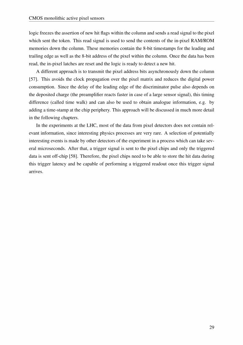
CMOS monolithic active pixel sensors
logic freezes the assertion of new hit flags within the column and sends a read signal to the pixel
which sent the token. This read signal is used to send the contents of the in-pixel RAM/ROM
memories down the column. These memories contain the 8-bit timestamps for the leading and
trailing edge as well as the 8-bit address of the pixel within the column. Once the data has been
read, the in-pixel latches are reset and the logic is ready to detect a new hit.
A different approach is to transmit the pixel address bits asynchronously down the column
[57]. This avoids the clock propagation over the pixel matrix and reduces the digital power
consumption. Since the delay of the leading edge of the discriminator pulse also depends on
the deposited charge (the preamplifier reacts faster in case of a large sensor signal), this timing
difference (called time walk) and can also be used to obtain analogue information, e.g. by
adding a time-stamp at the chip periphery. This approach will be discussed in much more detail
in the following chapters.
In the experiments at the LHC, most of the data from pixel detectors does not contain rel-
evant information, since interesting physics processes are very rare. A selection of potentially
interesting events is made by other detectors of the experiment in a process which can take sev-
eral microseconds. After that, a trigger signal is sent to the pixel chips and only the triggered
data is sent off-chip [58]. Therefore, the pixel chips need to be able to store the hit data during
this trigger latency and be capable of performing a triggered readout once this trigger signal
arrives.
29
Chapter 3
Design and characterisation ofradiation-hard CMOS sensors
3.1 Sensor technology
3.1.1 The standard TowerJazz 180 nm process
The monolithic CMOS sensors described in this work were fabricated in the TowerJazz 180 nm
CMOS process which was also used for the upgrade of the Inner Tracking System of the ALICE
experiment [59]. The sensors in this technology implement a small collection electrode to
achieve a small sensor capacitance, as described in sect. 2.3.1. A cross-section of a pixel
in the standard TowerJazz 180 nm process is shown in fig. 3.1 [60]. The charge generated
in the sensor is collected by the small n-well collection electrode. The electrode is separated
from the in-pixel electronics by several microns to reduce the lateral capacitance to the wells.
The n-wells of PMOS transistors are shielded by a deep p-well so that they do not compete
with the collection electrode in the charge collection. This allows the use of full CMOS and
therefore more complex readout circuitry in the pixel. The technology uses a 3 nm gate oxide
thickness and follows the general trend observed in many deep submicron CMOS technologies
for increased total ionising dose tolerance with decreasing gate oxide thicknesses [61].
The foundry also allows the use of different starting materials for the sensor, which means
that, for applications in a high-radiation environment, a high-resistivity p-type epitaxial layer
can be used to enhance the depletion around the collection electrode [62]. The designs dis-
cussed in the following sections use a 25-30 µm thick epitaxial layer with a resistivity of over
1 kΩcm. To further increase the depletion zone and further reduce the sensor capacitance, a
reverse bias of up to 6 V is applied to the p-type substrate of the sensor. Since the bulks of
NMOS transistors see the same reverse voltage applied to the substrate, this bias is limited by
the breakdown of the source/drain junctions of NMOS transistors, which occurs at around 8 V.
30

Design and characterisation of radiation-hard CMOS sensors
NWELL COLLECTION ELECTRODE
PWELLDEEP PWELL
P- EPITAXIAL LAYER
P+ SUBSTRATE
NWELL PWELL NWELLDEEP PWELL
PMOSNMOS
DEPLETION BOUNDARY
DEPLETED ZONE
Figure 3.1: Cross-section of a pixel in the standard TowerJazz 180 nm process (reproduced from [60]).
However, even with reverse bias, it is difficult to deplete the areas under the deep p-well, near
the pixel edges, and achieve full depletion of the sensitive layer. The signal charge generated
outside the depleted area is still collected primarily by diffusion, which results in a moderate tol-
erance to non-ionising radiation of up to 1013 neq/cm2. This is sufficient for the modest ALICE
requirements, but for a radiation tolerance up to 1015 neq/cm2 and beyond, for more demanding
applications, a drift field and depletion is required over the full sensitive layer. Increasing the
collection electrode helps to laterally extend the depletion region, but brings a significant ca-
pacitance penalty. Reducing the area of the in-pixel electronics also helps to create a potential
gradient, but this limits the amount of circuitry one can implement inside the pixel. Therefore,
a process modification has been introduced to achieve full depletion of the epitaxial layer.
3.1.2 Designs in the modified TowerJazz process
The idea behind achieving full depletion of the sensitive layer combined with a low capacitance
collection electrode is to implement a large or even planar junction separate from the collection
electrode. In this case, a low-dose deep n-type implant is used over the full pixel to create a
planar junction in the epitaxial layer, below the wells containing circuitry. This is depicted in
fig. 3.2. The depletion starts from the junction and immediately extends over the full pixel area.
The epitaxial layer is fully depleted even without reverse sensor bias. The n-type implant is
sufficiently low-dose to be fully depleted up to the n-well collection electrode for reverse bias
voltages of a few volts, and maintain a sensor capacitance of only a few femtofarads. This also
means that the collection electrodes in a pixel matrix are mutually isolated. The depletion layer
now also separates and isolates the p-wells containing the electronics from the substrate, which
means that they can be biased independently. The potential barrier created by the n− implant is
sufficient to apply a reverse substrate voltage of above 20 V for a 25 µm thick epitaxial layer,
while still avoiding punchthrough between the p-wells and the substrate. This further increases
the electric fields in the sensitive region and potentially leads to a faster charge collection.
31

Design and characterisation of radiation-hard CMOS sensors
LOW DOSE N-TYPE IMPLANT
NWELL COLLECTION ELECTRODE
PWELLDEEP PWELL
P- EPITAXIAL LAYER
P+ SUBSTRATE
NWELL PWELL NWELLDEEP PWELL
PMOSNMOS
DEPLETION BOUNDARY
DEPLETED ZONE
Figure 3.2: Cross-section of a pixel in the modified process [60]. The additional n-type implant allowsfull depletion of the sensitive layer.
Another advantage of this approach is that, apart from defining the region of the n− implant
over the pixel matrix, the process modification does not require any layout changes in the design
of the sensor or the circuitry. Therefore, the same design can be produced in both the standard
and the modified process, allowing a direct comparison between the two.
The Investigator chip [63] was produced to characterise the performance of monolithic
CMOS sensors implemented in the TowerJazz technology. The chip consists of a collection of
pixel sub-matrices which differ among each other in terms of a few parameters, some of which
affect the shape and extension of the depleted region: pixel size, electrode size, electrode-to-
deep-p-well distance. The analogue voltage signals from the collection electrodes are read out
using source follower buffers. A number of these chips have been characterised with a 90Sr
radioactive source, which emits electrons that traverse the sensor and generate a signal similar
to the response to minimum ionising particles [64]. Fig. 3.3 compares the signal amplitudes and
rise times of signals at the collection electrode for a 50×50 µm2 pixel size on an unirradiated
sample, a sample irradiated to a fluence of 1014 neq/cm2 and a sample irradiated to a fluence of
1015 neq/cm2. All samples shown were produced using the modified process and were tested at
a substrate bias of −6 V.
The curves in fig. 3.3a show the Landau spectra of the 90Sr source. In all cases, the peak of
Landau distribution is clearly separated from the noise peak located close to 0 mV of amplitude.
The red curve shows very good signal response and a signal loss of less than 20% after a
fluence of 1015 neq/cm2, much in contrast to a sensor in the standard process after this irradiation
fluence, from which no useful signal could be extracted anymore. The sensor maintains a fast
signal response even after a fluence of 1015 neq/cm2, as seen in fig. 3.3b. The time spread of
only σ = 2.78 ns is less than even the unirradiated sensor of the standard process, which gave
σ = 4.6 ns. Note that the rise time includes the charge collection time, but is also limited by the
speed of the source followers used to read out the signals.
32

Design and characterisation of radiation-hard CMOS sensors
Signal [mV]0 10 20 30 40 50 60
Rel
ativ
e fr
eque
ncy
0
0.005
0.01
0.015
0.02
0.025
0.03
0.035Unirradiated MPV = 18.937 +/- 0.122 mV
1e14 neq MPV = 19.499 +/- 0.147 mV1e15 neq MPV = 15.904 +/- 0.124 mV
Charge collection time [ns]0 10 20 30 40 50 60 70 80 90 100
Rel
ativ
e fr
eque
ncy
0
0.02
0.04
0.06
0.08
0.1
0.12
0.14
0.16
0.18
0.2
0.22
Vsub = -6V
Unirradiated Peak = 16.67 sigma 1.96 ns - sigma/peak = 11.76 %
1e14 neq Peak = 16.03 sigma 2.10 ns - sigma/peak = 13.10 %
1e15 neq Peak = 18.98 sigma 2.78 ns - sigma/peak = 14.63 %
Vsub = -6V
(a) (b)
(a)
Signal [mV]0 10 20 30 40 50 60
Rel
ativ
e fr
eque
ncy
0
0.005
0.01
0.015
0.02
0.025
0.03
0.035Unirradiated MPV = 18.937 +/- 0.122 mV
1e14 neq MPV = 19.499 +/- 0.147 mV1e15 neq MPV = 15.904 +/- 0.124 mV
Rise time [ns]0 10 20 30 40 50 60 70 80 90 100
Rel
ativ
e fr
eque
ncy
0
0.02
0.04
0.06
0.08
0.1
0.12
0.14
0.16
0.18
0.2
0.22
Vsub = -6V
Unirradiated Peak = 16.67 sigma 1.96 ns - sigma/peak = 11.76 %
1e14 neq Peak = 16.03 sigma 2.10 ns - sigma/peak = 13.10 %
1e15 neq Peak = 18.98 sigma 2.78 ns - sigma/peak = 14.63 %
Vsub = -6V
(a) (b)
(b)
Figure 3.3: Signal response of a sensor produced in the modified process before irradiation (blackcurve), after 1014 neq/cm2 (blue curve) and after 1015 neq/cm2 (red curve). Fig. (a) shows the amplitudedistribution for 90Sr source tests and fig. (b) shows the signal rise time [65].
The detection efficiency of the sensor is measured in a particle beam [65]. The chip is placed
between several reference detectors (a so-called beam telescope) which provide a 9 µm position
resolution for hits on the sensor surface. The efficiency is calculated as the ratio of the number
of events with telescope tracks and a corresponding sensor hit to the number of all events with
a telescope track. The detection threshold is set as low as possible while remaining above the
noise levels. For each of the measured Investigator sub-matrices, a 2×2 pixel group is read
out and the efficiency is plotted as a function of the hit position. The main results for samples
produced in the modified process are shown in figure 3.4. After correcting for edge effects due to
the telescope resolution, for unirradiated 50×50 µm2 pixels with a 3 µm electrode diameter and
18.5 µm electrode-to-deep-p-well spacing, the efficiency is found to be 98.5%± 0.5% (stat.)±0.5% (syst.). For 1015 neq/cm2 irradiated sensors with a 3 µm electrode and 3 µm spacing, the
measured efficiency is 98.5% ± 1.5% (stat.) ± 1.2% (syst.) for a pixel size of 25×25 µm2. In
both cases, the efficiency is uniform across the pixel surface. This suggests a negligible loss in
detection efficiency of sensors in the modified process even after irradiation to 1015 neq/cm2.
X [µm]-50 0 50
Y [ µ
m]
-50
0
50
Tra
cks
0
0.2
0.4
0.6
0.8
1
m Pitchµ50
Unirradiated
Pixel 1 Pixel 2
Pixel 3 Pixel 4
(a)
m]µX [-40 -20 0 20 40
m]
µY
[
-20
0
20 Tra
cks
0.5
0.6
0.7
0.8
0.9
1m Pitchµ252/cmeq1e15 n
Pixel 1 Pixel 2
Pixel 3 Pixel 4
(b)
Figure 3.4: Detection efficiency across the 2×2 pixel group for: (a) unirradiated 50×50 µm2 pixel with3 µm electrode and 18.5 µm spacing, (b) 1015 neq/cm2 irradiated 25×25 µm2 pixel with 3 µm electrodeand 3 µm spacing.
33

Design and characterisation of radiation-hard CMOS sensors
These encouraging measurement results prompted the design of full-scale prototypes in the
modified TowerJazz 180 nm process, which would meet the requirements of the outer pixel
layers in the ATLAS experiment in terms of detection efficiency, position and time resolution,
power consumption and radiation hardness. This would prove that monolithic CMOS sensors
are a feasible option for particle detection even in the most demanding environments with ex-
treme radiation levels.
The MALTA chip (short for "Monolithic from ALICE To ATLAS") is the largest monolithic
CMOS sensor designed to meet the ATLAS requirements. It contains a matrix of 512×512
pixels with a size of 36.4×36.4 µm2. The total chip size is around 2×2 cm2. The layout of
the full chip is shown in fig. 3.5. Apart from the large pixel matrix, the chip contains several
blocks to ease the operation of the chip and interface it with the outside world. The digital
periphery contains parts of the readout logic as well as the configuration registers used to tune
the various settings available on the chip. In the case of bias currents and voltages for the
front-end preamplifier, the register values are converted to the desired current or voltage values
using digital-to-analogue converters (DACs). The digital address and timing information of hit
pixels is transmitted off-chip through a 40-bit parallel output, which uses either a low-voltage
differential signal (LVDS) standard or a full-swing 1.8 V CMOS standard. The LVDS drivers
[66] designed to operate up to 5 Gb/s ensure robust data transmission to off-chip data acquisition
systems, while the CMOS input/output pads offer the possibility of chaining multiple chips
together and transmitting the hit data between chips.
18.6
mm
18.6 mm
power pads
CMOS in/out pads
DACs
digital periphery
LVDS output
Figure 3.5: Layout and main building blocks of the MALTA chip. The pixel matrix is divided into 8sectors with different sensor and front-end designs.
34

Design and characterisation of radiation-hard CMOS sensors
The pixel matrix itself is divided into 8 sectors with slightly different sensor and front-end
preamplifier designs. The sectors differ in the size of the collection electrode, which varies
from 2 to 3 µm in diameter and the spacing from the electrode to the surrounding deep p-well
containing the electronics, which varies between 3.5 and 4 µm. Another important difference
between the sectors is the deep p-well coverage inside the pixel. Specifically, since the deep p-
well is strictly needed only under the n-wells of PMOS transistors, half of the sectors implement
a "medium" deep p-well layout, where the deep p-well has been removed in areas with only
NMOS transistors which are still in the vicinity of the collection electrode. The other sectors
have a more conventional "maximum" deep p-well layout, where all transistors, NMOS and
PMOS, have a deep p-well underneath them. In terms of front-end design, the only difference
is the circuit used to reset the voltage of the collection electrode, which uses either a diode or a
PMOS transistor, as further described in the next section.
The in-pixel circuitry in MALTA is divided into an analogue part, which contains the front-
end preamplifier and discriminator, and a digital part, which contains the logic for reading out
the pixel matrix. The layout of a pixel is seen in fig. 3.6. As mentioned, the small collection
electrode in the middle is separated from the circuitry by up to 4 µm. The analogue and digital
regions are also well separated and shielded from each other with metals to avoid any crosstalk.
For the same reason, different power domains are used to provide the supply voltage to the two
regions. The designs implemented in both domains will be discussed in detail in the following
sections.
36.4
µm
digitalanalogue
collectionelectrode
36.4 µm
Figure 3.6: Layout of a pixel in the MALTA chip. The analogue and digital part are separated andshielded from each other and the collection electrode to avoid crosstalk.
35

Design and characterisation of radiation-hard CMOS sensors
3.2 Analogue front-end circuit
3.2.1 Principle of operation
The analogue part of the front-end circuitry implemented in MALTA contains the circuit to
reset the voltage of the collection electrode after a particle detection, a fast, low-power shaper-
amplifier and a simple discriminator. The front-end employs what is called a continuous reset
of the input node, i.e. the collection electrode, which means that the reset is not applied period-
ically to the pixels, but that the reset circuit is continuously active. Two different implementa-
tions of this continuous reset are present in the different sectors of MALTA.
A diode reset, shown in fig. 3.7a, uses the diode D1 to reset the collection electrode voltage
(node IN). When no charge is collected by the electrode, D1 is biased by the leakage current
of the sensor diode D0, which is typically in the order of femtoamps before irradiation. The
voltage of the electrode is then defined as the DAC voltage VRESET _D minus the voltage drop
across the reset diode, which is typically around 500 mV. When a particle is detected, the n-well
electrode collects electrons and its voltage will drop by ∆V = Q/C. This will cause the reset
diode to conduct more current and slowly charge the input node back up to its original value,
which can take several hundreds of microseconds.
The PMOS reset, shown in fig. 3.7b, uses a PMOS current mirror to perform the reset of
the input node. In this case, the DAC current IRESET defines the current used to charge the
input back up to its baseline. This current has to be larger than the leakage current of the sensor
diode. In steady-state conditions, M1 is forced to conduct the leakage current of the sensor,
which causes it to work in the linear region, and the voltage on the electrode is close to the
DAC voltage VRESET _P. After some charge is collected and the drain-source voltage of M1
becomes large enough to push it into saturation, the input node is reset with a constant current
IRESET − ILEAK .
(a) (b)
Figure 3.7: Two implementations of the circuit used to reset the voltage of the collection electrode (nodeIN): (a) diode reset, (b) PMOS reset.
36

Design and characterisation of radiation-hard CMOS sensors
The advantage of the diode reset is its simple implementation and low capacitance penalty,
since it can be implemented as a small p+ implant inside the collection electrode. However,
the conductance and hence the reset current changes significantly depending on the voltage
developed by the collected charge. The PMOS reset limits this current to IRESET and therefore
offers more control, but at the expense of more area and a larger input capacitance due to the
relatively large PMOS transistor and the metal connection to its drain.
The small electrode capacitance and high Q/C means that the voltage difference developed
on the electrode by collecting the charge deposited by a particle can already be quite large. In
the case of a 25 µm thick sensitive layer, the most probable value of the Landau distribution
for charge deposited by a minimum ionising particle is around 1500 e−. With a total elec-
trode capacitance of 5 fF this means a voltage step of around 50 mV. This offers the possibility
of using an open-loop voltage amplifier as the first amplification stage, instead of the conven-
tional charge-sensitive amplifier scheme with a feedback capacitor. This can simplify the design
somewhat and reduce the area required by the preamplifier/shaper circuitry.
The front-end amplifier designed for MALTA is an evolution of the front-end used in the
ALPIDE chip for the ALICE upgrade [67]. The operating principle of this amplifier is illus-
trated in fig. 3.8. The input node (gate of transistor M1) is connected directly to the collection
electrode. When the input voltage drops because of the collected charge, M1 acts as a source
follower biased by the current IBIAS. Therefore, a charge QS is transferred from a large capacitor
CS to a small capacitor COUT _A. Ideally, for the voltage on OUTA one can write:
∆VOUT _A =QS
COUT _A=
CS
COUT _A∆VIN =
CS
COUT _A
QIN
CIN. (3.1)
Figure 3.8: The operating principle of the MALTA front-end preamplifier.
37

Design and characterisation of radiation-hard CMOS sensors
This means that a high gain is obtained when CS COUT _A. In the actual circuit, CS is
implemented as a large PMOS transistor with its source, drain and bulk connected together
(using the capacitance of the MOS structure in inversion), while COUT _A includes only the
parasitic capacitances of transistors connecting to it. The full schematic of the actual front-
end amplifier and discriminator is shown in fig. 3.9. M0 is the current source providing the
IBIAS current of the input source follower M1. M1 is placed in its own n-well together with
the capacitor CS to provide a source follower gain close to 1. Transistors M5 and M6 provide a
low-frequency feedback to define the baseline voltage of OUTA and the return to baseline after a
particle hit. The bias voltage VCASN and the gate-source voltage of transistor M6 conducting the
current IT HR define the DC voltage on OUTA. The gate voltage of M3 (node GN) is adjusted in
a way that it sinks the current IBIAS+ IT HR. M2 is a cascode transistor used to prevent capacitive
coupling between the analogue output OUTA and the input, avoiding the Miller effect, and its
gate can be connected to the same GN node. When a particle crosses the sensor, the voltage
on OUTA rises, eventually forcing M6 out of saturation and forcing IT HR to charge up the GN
node. This results in a current increase through M3, which discharges the OUTA node and
brings it back to its baseline value. Note that here the capacitance CS plays the role of not only
the source capacitance of the follower determining the gain, but also the gate capacitance of M3
determining the return to baseline. The shape of the output signal can therefore be influenced
by IBIAS, IT HR and the value of CS in a way that the whole circuit acts as a band-pass filter with
a certain shaping time. Therefore, no additional shaping is needed after the OUTA node. An
additional feature to shorten the analogue pulse duration on OUTA for high input charges is the
clipping transistor M4, which starts conducting only when the OUTA voltage is above a certain
value. This value can be controlled using the VCLIP bias voltage.
Figure 3.9: Schematic of the actual front-end circuit implemented in MALTA.
38

Design and characterisation of radiation-hard CMOS sensors
Transistors from M7 to M9 form a simple discriminator, which can be viewed as a common-
source amplifier with a high gain. In steady-state conditions, the baseline voltage on OUTA sets
the DC current of M9 and the whole discriminator branch. M8 is again a cascode transistor to
reduce the Miller effect from the discriminator output OUTD to the amplifier output OUTA. M7
is biased to provide a current IDB higher than the DC current of the branch, but is pushed out of
saturation while OUTD is close to the supply voltage of 1.8 V. During the transient, when the
OUTA voltage increases, the current drawn by M9 increases to the point where it becomes larger
than IDB and starts discharging the OUTD node. As the signal on OUTA returns to its baseline
value, OUTD will be charged up again by the IDB current. The threshold of the discriminator is
therefore controlled by the combination of the DC current setting in the branch (so indirectly by
VCASN) and the IDB current setting. When the OUTD voltage drops below the threshold voltage
of the following inverter during the transient, a digital pulse is produced at the output of the
front-end.
The additional features implemented in the analogue part include pixel masking and test
pulse injection. The possibility of masking a pixel front-end is realised by adding three par-
allel NMOS transistors between to source of transistor M9 in the discriminator stage and the
analogue ground AV SS. The gates of these transistors are connected to digital signals used to
address the pixels that need to be masked. The addressing is done in a way that an address
line is provided for each of the 512 columns, rows, but also diagonals in the pixel matrix. By
tying one line in each of the three dimensions to ground, the three NMOS transistors in a single
pixel will be disabled and the discriminator output will be permanently tied to a high level, so
the front-end will never generate an output pulse. In other words, pixels at the intersections of
the vertical, horizontal and diagonal masking lines tied to ground will be deactivated. In the
case of masking multiple pixels, there is a chance of masking pixels which do not need to be
masked simply because they are located on the intersection of lines tied to ground. The diagonal
coordinate is needed to reduce the number of these unintentionally masked "ghost" pixels.
In a similar fashion one can select the pixels which are enabled for test pulse injection. Here
a diagonal line is not needed and the pixel is selected only by column and row selection bits.
The logic involved is depicted in fig 3.10. The digital VPULSE signal is propagated only to the
selected pixels, where two PMOS switches are tying the output of the pulsing circuit to one of
the two preset DC voltage levels: VHIGH or VLOW . On the rising edge of VPULSE , transistor M0
is switched off and M1 is switched on, so the output signal is a voltage step with an amplitude
of VHIGH −VLOW . This signal is then capacitively coupled to the input node of the front-end
through a 230 aF metal-to-metal capacitor CC. The amount of injected charge can then be
calculated as:
QIN =CIN∆VIN =CINCC
CIN +CC∆VOUT ≈CC (VHIGH−VLOW ) . (3.2)
39

Design and characterisation of radiation-hard CMOS sensors
The injected charge is therefore roughly 1.43 e− per mV of difference between the VHIGH and
VLOW DAC values.
Figure 3.10: Circuitry used to capacitively inject a test pulse to the input of the front-end.
3.2.2 Timing optimisation
One of the major changes in the front-end amplifier compared to the one in ALPIDE is that a
much faster signal rise time at the amplifier output needs to be achieved in order to meet the
ATLAS requirement for the 25 ns time resolution. Therefore, the shaping time of the front-
end has to be decreased from several microseconds to around 25 ns, which has far-reaching
consequences for several design parameters, such as power consumption, noise and mismatch.
To be able to achieve such a fast rise time, the total analogue power consumption has to be
increased by about an order of magnitude, since the IBIAS current in the main branch needs to
be around 500 nA to achieve a sufficiently large transconductance gm of the input device M1.
Since this transconductance controls the current used to charge the OUTA node in the initial
moments after a particle hit, until CS is discharged, the dimensioning of M1 is also critical: it
needs to have a high W/L ratio for a high gm and a total gate area large enough to avoid random
telegraph signal noise (RTS). However, the gate area must also remain small enough not to
dominate the input capacitance.
If M3 is made small enough, another effect becomes important, and that is the coupling from
the M1 source (node NW ) to the M3 gate (node GN) through the large capacitance CS. When
the voltage at the input drops, NW follows and via this coupling causes the VGS of M3 to drop
by several milivolts, effectively switching off M3 and again providing more current to charge
OUTA. Because of this, the gm of M3 also becomes important, so a large width of the device is
desirable. However, all the devices connecting to OUTA need to be kept quite narrow in order
to limit the increase of the parasitic capacitance on this node, which deteriorates not only the
gain but also the timing of the amplifier. For the same reason, the width of the discriminator
40

Design and characterisation of radiation-hard CMOS sensors
input M9 must not be increased too much, even though the high gm of this device is favourable
for the time response of the discriminator stage.
Keeping all this in mind, the transistors in the front-end are dimensioned to give the best
possible timing performance for a 500 nA bias current. Note that the total power consumption
of the front-end is some 10% higher due to the additional DC current in the second branch
(IT HR is typically only a few nA) and the discriminator branch (typically a few tens of nA).
However, with a supply voltage of 1.8 V, this still gives less than 1 µW of analogue power
consumption per pixel, which is far below any specification and at least an order of magnitude
below large collection electrode designs with similar shaping times [68]. The total analogue
power consumption is then around 75 mW/cm2. A simulation of the transient waveforms at the
input, analogue output and discriminated output of the front-end with the charge threshold set to
200 e− is shown in fig. 3.11. This threshold has been chosen to maintain full detection efficiency
with a Landau peak of around 1500 e−, taking into account potential charge sharing between 4
pixels and some charge loss after irradiation. The solid line shows the response for a collected
charge of 300 e−, the dashed line for a charge of 3000 e−. The simulation was performed by
modelling the input signal as a trapezoidal current pulse with a width of 1 ns, assuming a charge
collection time around that value. The sensor is modelled as a leakage current source in parallel
Figure 3.11: Simulated transient response of the MALTA analogue front-end circuit: (a) signals at thesensing node, (b) signals at the output of the amplifier, (c) signals at the output of the discriminator.
41

Design and characterisation of radiation-hard CMOS sensors
with a capacitance of 2.5 fF, which is a value previously measured on prototype chips [69].
The simulation also takes into account all the parasitic routing capacitances, which have been
extracted from the pixel layout.
The red curves show that the initial voltage step at the input is proportional to the charge,
and after the charge is collected the input node is slowly reset to its initial voltage (in this
case with a diode). The blue curves show the amplified signals at OUTA. Notice that the
pulse duration is actually shorter for an input charge of 3000 e−, which is a result of the signal
clipping mechanism described earlier. When the signals exceed a certain voltage level for which
IM9 > IDB, the discriminator fires, as seen in the green curves showing the discriminator output
signals. Here one can observe two quantities important to describe the timing characteristics of a
pixel front-end. One is the dead time, which is basically the duration of the discriminated pulse.
During this time, the front-end is insensitive to any new particle hits within the same pixel, since
they will not produce a new pulse and therefore will not be detected. Avoiding this analogue
pile-up is the main reason to limit the duration of the discriminator pulse. For the simulated
front-end settings, the maximum pulse duration is around 200 ns, which results in negligible
pile-up rates for hit rates in the outer pixel layers of ATLAS. The other important quantity is the
time walk, which describes the time difference in the leading edge of the discriminator pulse
for different amounts of charge collected. If no correction is made for it, the time walk is the
number that determines the time resolution of the front-end, and one would like to keep it below
25 ns for this application. The red curve in figure 3.12 shows the simulated time walk curve,
i.e. the delay of the discriminator leading edge versus the collected charge.
dela
y of
lead
ing
edge
(ns
)
0.0
10.0
20.0
30.0
40.0
50.0
60.0
70.0ga
in (
mV
/e-)
100.0
200.0
300.0
400.0
500.0
600.0
700.0
800.0
input charge (ke-)0.2 0.4 0.6 0.8 1.0 1.2 1.4 1.6 1.8 2.0 2.2 2.4 2.6 2.8 3.0
Figure 3.12: Simulated time-walk and gain curve for the front-end. The in-time threshold extracted fromthe red curve is 285 e−.
42

Design and characterisation of radiation-hard CMOS sensors
For charges very close to the threshold, this delay exceeds the 25 ns mark, but in this sim-
ulation, already 85 e− above the threshold the delay is within 25 ns of the minimum possible
delay. This means that all charges above 285 e− will be detected within the required time
window. This in-time threshold is a number often used to summarise the timing performance
of detectors at the LHC. Again, with a most probable charge deposition value of 1500 e−, an
in-time threshold of 285 e− should give very close to full in-time efficiency for the detector.
The blue curve in 3.12 shown the gain of the amplifier expressed in mV per e− of input
charge. The circuit has a non-linear gain characteristic and the analogue output saturates al-
ready above approximately 300 e− of input charge for these settings, partly due to the clipping
transistor starting to conduct significant current. The gain is high enough to be able to achieve
the desired low operating charge thresholds by tuning the discriminator threshold, even down
to 100 e−, which would even further improve the in-time efficiency of the circuit.
3.2.3 Noise and mismatch
Equation 2.21 discussed in sect. 2.3.1 concerning the thermal noise of the input transistor is
also valid for this circuit. The small sensor capacitance and high transconductance of the input
device inherently provide a good noise performance. The current sources are all made narrow
and long to reduce their noise contributions. To check which devices contribute to the total noise
seen at the output of the amplifier, a linearised AC noise analysis is performed at threshold. Note
that even with the non-linear transfer function evidenced by fig. 3.12, this analysis gives fairly
accurate results for charges close to threshold. The results are summarised in table 3.1.
Table 3.1: Simulated noise contributions of transistors in the front-end.
Device Noise type Noise contribution (mVRMS) Percentage of total (%)
M1 thermal noise 3.29 38.21
M3 thermal noise 2.83 28.09
M3 1/f noise 2.34 19.19
D1 shot noise 1.18 4.87
M6 thermal noise 1.09 4.17
M5 thermal noise 1 3.52
The thermal noise of the input device M1 is indeed the dominant contributor. Apart from
the thermal noise, the 1/f noise (attributed to imperfections and the generation/recombination
of charge carriers in the channel) of M3 also has a non-negligible contribution due to the gain
mechanism described earlier. D1 represents the shot noise of the reset diode, which is asso-
ciated with fluctuations when a current flows across a p-n junction, and is proportional to the
43

Design and characterisation of radiation-hard CMOS sensors
current flowing through the device, in this case the sensor leakage current. The simulation was
performed with a leakage current of 10 pA, which is an overestimation before irradiation, but
the leakage current of irradiated sensors might even exceed that value, especially at room tem-
perature, where the shot noise could become the dominant contributor. To include the shot noise
of the sensor diode, one also needs to multiply this value by roughly√
2. The RMS value of
the total equivalent noise voltage on OUTA is calculated to be 5.22 mV. When compared to the
signal amplitude at threshold, which is simulated to be 143.59 mV, a signal-to-noise ratio of
27.5 is obtained.
For a more accurate estimation of the equivalent noise charge referred back to the input
and the S/N, a transient noise simulation can also be performed. By sweeping the input charge
around threshold, running multiple simulations for each charge and looking at the probability of
a discriminator hit occurring for a given charge, a noise S-curve shown in fig. 3.13 is obtained.
This curve is essentially the integral of the Gaussian noise distribution around threshold. There-
fore, the 50% value of the probability curve gives the mean threshold value, while the RMS
of the normal noise distribution represents the ENC. As expected, the mean threshold value is
close to 200 e−, while the ENC is around 7 e−. This gives an S/N of 28.8, which matches the
results of the linearised analysis fairly well. One can conclude that an even lower operating
threshold than 200 e− should indeed be possible, since with any threshold larger than 10σ of
the noise one should expect close to no noise hits even in a large pixel matrix.
160 170 180 190 200 210 220 230 240
input charge (e-)
0
0.1
0.2
0.3
0.4
0.5
0.6
0.7
0.8
0.9
1
hit p
roba
bilit
y
Noise S-curve for front-end
datafitted curve
QTH = 198.87 e-ENC = 6.91 e-
Figure 3.13: Simulated noise S-curve for the front-end. The RMS value of the fit yields an equivalentnoise charge of around 7 e−.
A similar type of S-curve can be obtained when simulating the pixel-to-pixel differences
between front-ends due to random process variations and transistor mismatch. The mismatch
44

Design and characterisation of radiation-hard CMOS sensors
160 170 180 190 200 210 220 230 240
input charge (e-)
0
0.1
0.2
0.3
0.4
0.5
0.6
0.7
0.8
0.9
1
hit p
roba
bilit
y
Mismatch S-curve for front-end
datafitted curve
QTH = 199.22 e-RMS = 7.81 e-
Figure 3.14: Simulated mismatch S-curve for the front-end. The RMS value of the fit yields around 8e− of threshold variation at a 200 e− threshold.
S-curve obtained in Monte Carlo simulations using the models for threshold voltage variation
provided by the foundry is shown in fig. 3.14. In this case, the RMS value of the curve represents
the charge threshold variation between pixels and is close to 8 e− in this simulation. To obtain
such a low threshold variation, special care needs to be taken of the sizing of critical devices.
From theory, it is well-known that the threshold voltage variation σV T H of transistors scales
with 1/√
WL [70]. Therefore, to reduce the total variation in the circuit one has to increase
the total area of critical devices. In the case of the front-end discussed here, these devices are
mainly M5 and M6. The IT HR current of M5 has a big influence on the gain of the amplifier,
and both these devices are defining the DC current of the discriminator and hence its switching
threshold. This is made even more prominent by the fact that these two devices work with very
low currents and in weak inversion, where the conversion from threshold voltage variation to
current variation is exponential. For this reason, M5 is by far the largest transistor in the front-
end layout with a total area of 20 µm2. M6 should not be increased to that extent because of the
capacitance penalty on OUTA, but an area of 1 µm2 is a good trade-off. This leaves M3 and M9
as the dominant sources of charge threshold variation, but again, these have to kept quite small
not to load the OUTA node too much.
Since the simulated threshold variation is already very low and comparable to the noise
levels, the decision has been made not to include any per-pixel threshold tuning capabilities in
the pixel matrix. Therefore, only the global threshold value of the chip can be tuned using the
various DAC settings for the front-end.
45

Design and characterisation of radiation-hard CMOS sensors
3.2.4 Considerations for radiation hardness
As mentioned earlier, to keep the front-end functional even after high non-ionising fluences,
one has to make sure that the input stages of the front-end can operate in a wide range of sensor
leakage currents. The expected leakage current values after irradiation to 1015 neq/cm2 are in
the range of several hundreds of picoamps at room temperature. Even though the detectors are
operated at a low temperature of −30, this needs to be taken into account during the design.
In particular, the range of the IRESET current used in the sectors with PMOS reset needs to be
high enough to go beyond these leakage values. As for the diode reset, for high leakage currents
the reset diode becomes highly conductive and can reset the input signal too quickly, clipping
the voltage signal and effectively causing part of the signal to be lost. At a leakage current of
100 pA, however, the loss in signal because of this clipping effect is only about 5%, so at low
temperatures this is not an issue. The VRESET _D voltage also provides a handle to tune the DC
voltage at the front-end input, giving sufficient margin to keep all transistors in the first branch
in saturation for a wide range of sensor leakage currents.
As far as tolerance to ionising radiation is concerned, it is important to make sure that
transistor leakage currents induced by positive trapped charge in the field oxide do not affect
the operation of the circuit significantly. The changes in drain current are not likely to affect
the behaviour of devices conducting currents of tens or hundreds of nanoamps. However, since
the IT HR current can be even below 1 nA, M5 and M6 are again the devices most sensitive
to TID. Leakage current increases in the order of 100 pA have been measured for minimum
size NMOS transistors in the TowerJazz 180 nm technology after 20 Mrad of TID [71]. The
expected ATLAS levels are a factor of 3-4 higher than that, so the M6 NMOS transistor in the
sensitive IT HR branch could well be affected. Because of that, this transistor is implemented
with an enclosed layout. This introduces an additional constraint on the sizing of this device,
since the width is no longer independent of the length. Therefore, quite a wide device has to
be used to limit its threshold voltage variation, which increases the capacitance on the analogue
output and brings a slight penalty in terms of speed. A p+ guard ring is also added around
the device to prevent any leakage to neighbouring devices, which more or less doubles the area
required for this transistor. However, it is a necessary step to ensure sufficient radiation hardness
of the front-end up to the required 50 Mrad of TID.
3.2.5 Bias generation using digital-to-analogue converters
The current and voltage biases for the front-end are generated using 7-bit digital-to-analogue
converters. The basic operating principle of the current DACs is shown in fig. 3.15. A reference
current IREF of 140 nA is generated using a simple current generator with a diode-connected
PMOS transistor M0 in series with a 60 kΩ resistor. This current is then mirrored to 127 DAC
46

Design and characterisation of radiation-hard CMOS sensors
units. Each unit contains a transmission gate switch, S1, which is open or closed depending on
the desired DAC code. The 7-bit code is stored in registers at the digital chip periphery, and
is thermometer encoded to close the number of switches corresponding to the decimal value of
the binary code. The configuration registers are triplicated to prevent single-event upsets. All
127 units are connected to the drain of a diode-connected NMOS transistor M2, so the current
of all units where S1 is closed is summed up and mirrored to one or two more stages. The
mirroring ratio in these stages determines the final range and current step (or least significant
bit, LSB) of a particular DAC. All NMOS transistors in these mirroring stages have an enclosed
layout to avoid leakage problems after TID. For the same reason, all the current sources in the
front-end are PMOS transistors, so the last mirroring stage contains the PMOS transistor M4,
whose gate/drain is then connected to the gates of current sources within the pixel matrix. Even
though the DAC uses its own power supply domain, the source of this last PMOS is connected
to the analogue supply of the matrix in order to avoid any current variation due to the voltage
drop along the supply lines in the matrix. Since the power pads are distributed along the left and
right side of the matrix, the vertical voltage drop between rows should be negligible. However,
with a current consumption of 500 nA/pixel and a width of 8.5 µm available for the horizontal
metal lines used for power supply routing, a voltage drop of around 6 mV is estimated, which
could cause a significant current and charge threshold mismatch. Therefore, compensation for
power supply voltage drop by means of using the matrix supply domain for the last mirroring
stage is necessary to avoid a systematic threshold gradient along the matrix width.
Figure 3.15: Operating principle of the current DACs in MALTA. The reference current is mirrored witha certain ratio to give the desired bias current values.
The voltage DACs are implemented as a string of resistors connected between power supply
and ground, as seen in fig. 3.16. This gives an LSB of 1.8/127 = 14.2 mV for all the voltages.
Again, the DAC code is stored in triplicated registers, but this time one-hot encoded to close
only one out of the 128 switches, thus choosing the desired voltage value within the resistive
47

Design and characterisation of radiation-hard CMOS sensors
divider. This voltage is either connected directly to the transistor gates within the pixel matrix,
or buffered with a source follower in case a significant current needs to be provided (like e.g.
the reset voltages which need to be able to source the full sensor leakage current for all pixels).
Figure 3.16: Operating principle of the voltage DACs in MALTA. Some of the voltages are bufferedwith a source follower before connecting to the pixel matrix.
An exception among the voltage biases is the VCASN voltage for M6 in the front-end. For
this voltage, a compensation for voltage drops along the ground line is needed, since with the
same VCASN over the full matrix this would cause a difference in the VGS of transistor M9 in the
front-end, resulting in a significant threshold gradient for the discriminator. A simple circuit
implemented to carry out this compensation is shown in fig. 3.17. An ICASN current is used
generate the VCASN voltage through two diode-connected NMOS transistors. Both the power
supply and ground of the circuit are connected to the analogue supply and ground of the matrix.
With appropriate dimensioning of the transistors in the circuit and assuming ICASN IT HR, the
generated VCASN will adjust the steady-state current in the discriminator stage of the front-end
to approximately match ICASN regardless of any voltage drops on the ground line. For this to
Figure 3.17: Circuit used to generate the VCASN bias voltage from the ICASN current.
48

Design and characterisation of radiation-hard CMOS sensors
work, M1 and M3 in the biasing circuit need to see the same bulk voltage as the corresponding
transistors in the front-end, and hence their bulks need to be connected to the p-well potential
of the matrix. This way, the DC current and threshold of the discriminator will not change
significantly with voltage gradients on the ground line nor changes in the p-well bias.
An additional safety feature implemented for all DACs is the possibility to monitor and/or
override the internal DAC values through a special set of pads. This allows to measure the
current and voltage values generated by the DACs to perform e.g. DAC linearity checks. It also
allows to force the currents and voltages externally in case of a problem in the operation of the
DACs or the configuring logic.
3.3 Digital readout electronics
3.3.1 Asynchronous matrix readout
The MALTA chip uses a novel asynchronous digital readout architecture without propagating a
clock to the pixel matrix in order to reduce the digital power consumption. For the readout, the
512×512 pixels in MALTA are organised in double columns, and within a double column in
sets of 2 (columns) by 8 (rows). Alternating sets of 16 pixels are connected to two output buses
per double column, as depicted in fig. 3.18 [57]. When a discriminator of a pixel within a set
of 16 pixels is fired, it activates a reference or hit signal, the one line out of 16 corresponding to
the hit pixel, and the 5-bit group address corresponding to the set of 16 pixels where the hit was
detected. A pulse with a length programmable to 0.5, 0.75, 1 or 2 ns is transmitted in parallel
on every line which needs to transmit a logic one. The delay in the transmission line is matched
between the different lines on the bus, and the total number of lines per bus is 22 (1+16+5).
In case charge is shared between two or more pixels in a group, a hit arbitration is performed
within the group to ensure that the hit data of all fired pixels is transmitted correctly. If the
discriminators of two pixels fire simultaneously, two corresponding lines are activated and only
one word is transmitted on the bus. If the pixels receive a sufficiently different amount of charge
and the discriminators react one after the other, two words are transmitted sequentially over the
bus, guaranteeing sufficient separation of the pulses on the bus for proper transmission. The
groups of 16 pixels in a double column are alternated between the two output buses (red and
blue in fig. 3.18) to prevent data collisions if a particle hits at or near the boundary between
two different groups. Data is transmitted almost instantaneously, and is therefore available at
the periphery only a few nanoseconds after the hit took place. The readout of each double
column is completely independent of the others, so that multiple columns can transmit data at
the same time. This massive parallelism in the matrix provides a very high bandwidth necessary
for high-rate applications [72].
49

Design and characterisation of radiation-hard CMOS sensors
32 b
lue+
32 re
d pi
xel g
roup
s of 2
x8 p
ixels
= 1
doub
le co
lum
n 2x
512
Pixel bus 16 bits Group addr.5 bits
Pixel bus 16 bits Group addr.5 bits
16 li
ne p
ixel b
us
16 li
ne p
ixel b
us
5 bi
t gro
up #
bus
5 bi
t gro
up #
bus
Ref. Ref.
Figure 3.18: Organisation of a double column in the MALTA digital readout architecture [57].
Knowing the average number of bits toggling to be 4.5 (1 reference bit, 1 pixel bit and an
average 2.5 out of the 5 group bits), one can calculate the power consumption needed to transmit
the matrix data for a given hit rate. An example of this is shown in table 3.2, where the digital
power consumption is calculated for the expected hit rates in different layers of the ATLAS
ITk [73]. The energy needed to toggle 1 cm of line can be calculated as CV 2, which in this
technology yields 6.5 pJ/cm. Multiplying this by the expected hit rates and average number of
toggles gives an estimate of the total digital power consumption needed for the asynchronous
readout of the MALTA matrix.
Table 3.2: Matrix readout power calculated for different hit rates (reproduced from [73].
Layer Pixel hit rate(MHz/mm2)
Power/bit(mW/cm2)
Matrix readout power(mW/cm2)
0 27.2 17.7 79.6
1 8.4 5.4 24.6
2 1.72 1.1 5.0
3 1.16 0.8 3.4
4 0.84 0.5 2.5
50

Design and characterisation of radiation-hard CMOS sensors
For comparison, the power needed to transmit a 40 MHz clock over 1 cm2 with a pixel pitch
of 36.4 µm using the same calculation is found to be 36 mW/cm2. This doubles if the clock
signals are transmitted differentially, which is often the case to achieve better robustness of the
signal transmission. It is evident that the power for the clock transmission itself is comparable
to the readout power even for the highest hit rates in the innermost pixel layers, and is more
than an order of magnitude higher than the readout power in the outer layers. Therefore, the
asynchronous approach does provide a significant power reduction.
The in-pixel logic used for the generation of the transmitted pulses and for hit arbitration
in case of multiple hits in a group is shown in fig. 3.19. When the front-end detects a hit and
produces an output pulse (node IN for the digital readout logic), a logic one will be latched by
the D flip-flop on the right in the double flip-flop structure shown in fig. 3.19a, since the initial
value of the RESET , MIRROR and VALID signals is 0. The STAT E signal goes to a high level
and a logic one is latched by left flip-flop, causing MIRROR to go to a high level as well. The
(a)
(b)
Figure 3.19: A simplified view of the in-pixel readout logic implemented in MALTA: (a) double flip-flopstructure for hit arbitration (b) pulse generator circuit used to generate the reference pulse.
51

Design and characterisation of radiation-hard CMOS sensors
VALID signal is in common for all the pixels within a group of 16, and goes to a high level if
any of the STAT E signals for the 16 pixels are high, disabling the latching of further hits until
the first hit is read out. It also starts the generation of the reference pulse in the circuit shown in
fig. 3.19b. The VALID signal is inverted, delayed and then combined with the original signal to
obtain a short pulse on REF_B, which is the inverted version of the reference pulse transmitted
down the column. The procedure is repeated once more to obtain a similar pulse on RESET
immediately after the reference pulse. The duration of the reference and RESET pulses can be
tuned using 4 control bits which act on the number of delay stages used within the delay cells,
resulting in a pulse width between 500 ps and 2 ns. The reference pulse is combined with the
STAT E signals from all 16 pixels, generating the 16-bit pixel address, as well as 5 hard-wired
group bits fixed for each of the 32 groups, which generates the 5-bit group address. Once the
RESET pulse is generated, the and/or logic in fig. 3.19a will cause the MIRROR_B signal, now
a logic zero, to be latched by the flip-flop on the right, effectively resetting the STAT E signal.
The MIRROR signal will be reset as soon as the input signal goes down, and at this point the
in-pixel logic will be ready to detect a new hit.
Note that if another pixel is fired within the same group and within a time window of around
1 ns with respect to the first fired pixel (typically because of two pixels collecting a similar
amount of charge and their discriminators firing nearly simultaneously), the STAT E signal will
be generated for both pixels, and the two pixel address pulses will be sent with the same refer-
ence signal, as one data word. If the delay between input signals in larger than 1 ns, the VALID
signal from the first hit will have already blocked the generation of the STAT E signal for the
second hit, so this hit has to be read out in the next read cycle, with a second reference pulse.
This is the case in the simulation shown in fig. 3.20. The second front-end output, IN[1], fires
1.5 ns after the first one, IN[0]. Therefore, the STAT E[0] signal goes high first, closely followed
by MIRROR[0] and VALID. Because VALID is high, another STAT E signal can not be gen-
erated, and the VALID starts the pulse generation circuit, producing the REF reference pulse.
This is combined with STAT E[0] to produce the pixel address bit PIX [0], as well as the hard-
wired group bits to produce the binary encoded group address. As the simulation is performed
for group number 31, all five group bits will produce a pulse (only GROUP[0] is shown). The
width of the pulses is set to 1 ns. The RESET signal will cause the VALID signal to go to a low
level, now allowing the generation of the STAT E[1] signal for the second fired pixel. Again,
the correct pixel address, PIX [1] is transmitted, and the STAT E and VALID signals are back to
their initial value. The MIRROR signals will be reset with the falling edge of the input signal,
which in this case occurs after 100 ns, outside the simulation window.
The pulses generated in the pixel are transmitted down the column using a special buffering
structure, shown in fig. 3.21. The input in this case is any one of the 22 reference/address bits
from the pixels (the buffering structure is the same for all the bits). As mentioned, there are two
52

Design and characterisation of radiation-hard CMOS sensors
IN<0>
IN<1>
REF
PIX<1>
PIX<0>
GROUP<0>
VALID
STATE<0>
MIRROR<0>
STATE<1>
MIRROR<1>
RESET
time (ns)40.0 43.0 46.0 49.0 52.0 55.0 58.0 61.0 64.0 67.0 70.0
Figure 3.20: An analogue simulation of the signals in the in-pixel readout logic in the case of two pixelhits within the same group separated in time by 1.5 ns. Two reference signals of 1 ns width are sent downthe column.
separate 22-bit buses for alternating groups of pixels: the "blue" groups (A) or the "red" groups
(B). In each "blue" group, the pulse is injected into one input of a NAND gate, while the other
input is used to propagate pulses coming from higher up within the matrix. The output of this
gate is then inverted in the next "red" group to achieve the correct polarity of the signals when
they reach the next "blue" group. The procedure is repeated over the full height of the column,
and is analogous for pulses generated in the "red" groups.
...
...
...
...
Figure 3.21: Chain of NAND gates used to buffer the signals down the column.
A critical goal in the signal propagation down the column is to preserve the pulse width and
the alignment of pulses on different lines of the bus. To achieve that, a special routing structure
53

Design and characterisation of radiation-hard CMOS sensors
needs to be used to exactly balance the capacitances at the output of each NAND gate. This
means not only using routing lines of the same width and length, but also distributing them
equally over the different metal layers, since different layers will see a different capacitance
e.g. to the top metal used for power routing. Even a small difference in capacitance causes
a delay difference between different bits which accumulates over the full height of the matrix
and can cause pulses of the same word to reach the end-of-column significantly misaligned in
time. Another concern is that if neighbouring lines are transmitting pulses simultaneously, they
effectively see a smaller capacitance compared to other lines. Because of that, one has to make
sure that neighbouring pixels, which could transmit simultaneous signals if they belong to the
same cluster caused by charge sharing, never use neighbouring lines for the transmission. In the
case of the group bits, the appearance of simultaneous pulses on the lines can not be avoided,
so these lines are shielded from one another. To avoid the deformation of pulses during the
transmission, one not only needs to balance the capacitances on the outputs of different NAND
gates, but also the delay of the rising and falling edge of the signals. If this is not the case,
the pulses could be significantly stretched or could even disappear completely by the time they
reach the end-of-column, depending on which edge has a smaller propagation delay. This is the
reason for using inverting gates (NAND instead of AND) in the transmission, and also why the
simple inversion in the opposite groups is done using the same NAND gates with one input tied
to a high level. This way, the rising edge in one NAND stage becomes the falling edge in the
next, so the edge delays are balanced by design and do not rely on the sizing of the gates. In this
case, changes in propagation delay caused by reverse bias on the bulks of NMOS transistors do
not deform the pulses either.
Extraction of the routing capacitances from the layout of two consecutive groups shows a
maximal capacitance difference between lines of less than 3%, resulting in a simulated maximal
delay difference of around 150 ps over the full column height. On the other hand, the maximal
deformation of the pulse width over the full column is only around 30 ps. As for the time it
takes transmit a pulse over the full column, from the top group to the bottom of the matrix, this
value is simulated to range from 7.2 ns without reverse bias on the p-well up to around 8 ns
with a p-well bias of −1.8 V.
3.3.2 End-of-column readout logic
At the end-of-column, in the digital chip periphery, signals from the two buses for the "red" and
"blue" groups are merged onto a common bus. For the case of simultaneous pulses on the two
buses, an arbitration logic similar to the one in the pixel is implemented to give priority to one
of the buses and delay pulses from the other bus. A delay counter bit is added to the address
bits, which transmits a pulse together with the delayed address pulses to signify that there were
simultaneous hits. This is done to be able to trace back the information about the time of arrival
54

Design and characterisation of radiation-hard CMOS sensors
of hits more precisely in case they need to be delayed. Since the MALTA architecture does not
encode time-over-threshold information, but uses a so-called binary readout of the matrix, the
time of arrival of hits can be useful to obtain relative information about the charge collected
by pixels within a cluster (because of time walk, hits from pixels collecting a high charge will
arrive before hits from pixels collecting charge values close to threshold). This is why it is
important to keep track of the delays using the delay counter during this time-ordering process.
An additional feature is the inclusion of another 2-bit counter running at 40 MHz used as a
bunch crossing identifier (BCID). This allows the hits to be timestamped and resolved within 4
bunch crossings (100 ns), which can be a useful feature to test the timing properties of the chip.
Finally, a group identifier bit is added to the data word, which indicates whether the hits came
from a "red" group or a "blue" group.
This process of merging and delaying pulses is repeated in a binary tree-like structure, as
shown in fig. 3.22, until hits from the full pixel matrix are merged onto a single bus. In each
level, a double-column identifier bit is added, so that the final data word unambiguously contains
the address of the hit pixel. In the second level, the delay counter is also expanded to 3 bits,
increasing every time a pulse is delayed, which means that a pulse can be delayed by a maximum
of 8 times in the 9 levels of merging. An additional tenth merger level is added for the possibility
to merge signals coming from multiple chips (as mentioned, data can be transmitted from chip
to chip through the CMOS data pads). Here, a 4-bit chip identifier is added, so that theoretically
up to 16 chips can be connected together. This creates the final 40-bit output data word of
MALTA, which contains 1 reference bit, 16 bits for pixel address, 5 for the group address, 1
group identifier bit, 3 bits for the delay counter, 8 for the double-column address, 2 for the
BCID and 4 for the chip address. This is summarised in table 3.3. 40 parallel LVDS drivers are
used to transmit the 40 signals off-chip. The drivers are designed to operate at up to 5 Gb/s with
a peak-to-peak jitter below 30 ps, and are more than capable of transmitting even the shortest
500 ps wide pulses.
Hit merger:Time-orders hits from 2x22 bits on 1x22 bits + group identifier + delay counter bit
LEVEL 1 LEVEL 2
...
...
Hit merger:Time-orders hits from 2x22 bits on 1x22 bits + group identifier + delay counter bit
Hit merger:Time-orders hits from 2x22 bits on 1x22 bits + double-column identifier + delay counter bits
Figure 3.22: Organisation of the hit merging circuitry at the end-of-column.
55

Design and characterisation of radiation-hard CMOS sensors
Table 3.3: Bits of the final output word of MALTA.
Bits Contents
0 Reference
1-16 Pixel address
17-21 Group address
22 Group identifier
23-25 Delay counter
26-33 Double-column address
34-35 BCID counter
36-39 Chip identifier
A simplified view of the logic used to merge and time-sort the reference pulses coming from
the matrix is depicted in fig. 3.23. Two flip-flops are reserved for pulses coming from each of
the two buses ("red" and "blue", A and B). This is done to be able to store consecutive pulses
from a single bus in case the other bus has priority and data from it is being transmitted further.
A toggle signal chooses the flip-flop used to latch the signals from each bus. This alternating
storage allows the transmission of up to 6 consecutive pulses coming simultaneously from both
buses before the logic is saturated. Similarly to the in-pixel logic, if any of the STAT E signals
Figure 3.23: A simplified view of the logic used to merge and time-sort the incoming reference signalsat the end-of-column.
56

Design and characterisation of radiation-hard CMOS sensors
is activated by latching an incoming reference signal, the VALID signal goes high and starts the
pulse generator, which is the same as the one used in the pixel and shown in fig. 3.19b. The
generated reference pulse is combined with a STAT E signal chosen by the priority logic and
transmitted to the next merger level. The priority logic also makes sure that the RESET signal
resets the correct flip-flop, namely the one that was given priority for transmission. After that,
the flip-flop is ready to latch another incoming pulse. The same logic is used to merge all the
other address bits and transmit them to the next merger level.
As a backup feature, a much more simple way of merging the hits from the matrix is also
included in the peripheral readout logic. This consists of a binary tree of OR gates for each
bit, which basically merge all the pulses coming from the full pixel matrix, but without any
arbitration in case of simultaneous hits. For reasonably low hit rates, this provides the same
functionality as the more complicated merger logic. However, in the case of simultaneous hits
appearing on multiple buses, combining the address bits with an OR gate will cause a corruption
in the address data. Therefore, for high hit rates this mode of operation could cause data loss
and hence a loss in detection efficiency.
3.4 Sensor characterisation before irradiation
3.4.1 Sensor and analogue performance in lab tests
The fabricated MALTA chips have been extensively tested in lab measurements and beam tests.
The chips are wirebonded to a printed circuit board (PCB) and the LVDS data output is con-
nected to an FPGA board used as a data acquisition system and interfaced with a computer
where the data is stored.
An early test is to plot the I-V characteristics of the sensor. As already explained, in the
modified process the additional n− layer isolates the p-wells of the electronics inside the pixel
matrix from the p-type substrate of the sensor. Therefore, the two can be connected to different
potentials, namely PWELL and SUB. However, if the difference between the two potentials is
too large, the n− layer does not provide a sufficient potential barrier and a significant current
flow can occur between the p-wells and the substrate. This is referred to as punchthrough. The
I-V curves at room temperature, i.e. the currents measured on the PWELL and SUB nodes
versus the reverse SUB voltage, and also for several reverse PWELL voltages, are plotted in
fig. 3.24. At low absolute values of the SUB voltage, the leakage current is close to constant
and is equal to about 4 µA for the substrate and 100 µA for the p-well at a p-well voltage of
−6 V. Note that this includes not only the leakage current of the sensor diode, but also any
other leakage between various wells on the whole chip. Above an absolute substrate voltage of
around 25 V, a sharp increase in the SUB current and a sharp decrease (and change of sign) in
57

Design and characterisation of radiation-hard CMOS sensors
the PWELL current can be observed. This indicates that there is a current flow between the two
nodes, which marks the onset of punchthrough. This typically happens at lower voltages than
the breakdown voltage of the sensor junction, so in this case it is the punchthrough that limits
the maximal sensor voltage that can be applied.
0 10 20 30 40 50VSub [V]
101
102
103
104|I S
ub| [
uA]
W7R12 T=25
0 10 20 30 40 50VSub [V]
10 -1
101
103
|I Pwe
ll| [u
A]
VPwell=2 VVPwell=4 VVPwell=6 V
VPwell=2 VVPwell=4 VVPwell=6 V
Figure 3.24: Sensor leakage current measured on the SUB and PWELL nodes with varying SUB voltage.
To test the performance of the analogue front-end, a special set of pixels has been included
on the side of the matrix, which allows the monitoring of the analogue output signals (OUTA)
of the front-end amplifier. The output signals are buffered and connected to a pad using two
stages of source followers with a gain close to 1 and with a marginal effect on the OUTA ca-
pacitance. The bias currents of the followers are adjusted to obtain a fast rise time, and the
waveforms are monitored on an oscilloscope with a low-capacitance active probe, so as not to
distort the signals. These monitoring pixels are available for both variations of the front-end
circuit, namely the one with a diode reset and the one with a PMOS reset. Fig. 3.25 shows the
amplitude distributions of the analogue output signals for the two flavours obtained during an
exposure of the chip to an 55Fe radioactive source. The 55Fe isotope decays by emitting x-rays
of two characteristic energy peaks: a K-α peak at 5.9 keV and a K-β peak at 6.49 keV with
a probability about 10 times lower than the K-α. These x-rays deposit a localised charge of
1640 e− and 1800 e− in the silicon sensor, respectively. The two peaks can clearly be seen
in both amplitude distributions. For this measurement, the clipping transistor in the front-end
58

Design and characterisation of radiation-hard CMOS sensors
has been deactivated not to saturate the gain of the amplifier prematurely. The VRESET _D and
VRESET _P settings were optimised for the highest gain, and all other settings were kept the same
for the sake of comparison. Both the SUB and PWELL voltages were kept at −6 V for this
test. The K-α peak is shifted from about 406 mV in the diode reset sector to about 353 mV in
the PMOS reset sector. This means that, for the same deposited charge of 1640 e−, the front-
end with diode reset produces a factor of 1.15 higher signal than the one with PMOS reset, as
expected due to the higher input capacitance introduced by the reset PMOS transistor.
150 200 250 300 350 400 450
amplitude (mV)
0
50
100
150
200
250
num
ber
of h
its
55Fe spectra from amplifier output
diode resetPMOS reset
7 = 353.4 mV< = 4.3 mV
7 = 405.6 mV< = 4.9 mV
Figure 3.25: 55Fe source spectra obtained from the monitored analogue outputs of front-ends with diodeand PMOS reset.
The width of the amplitude peak gives an estimation of the noise and the energy resolution
of the front-end. After correcting for the Fano factor, which describes the resolution of the
sensor itself (as mentioned in sect. 2.1), an RMS noise value of around 14 e− is obtained
for both sectors. This is higher than the simulated noise values for the front-end, which is
not surprising given that this includes the noise of the following buffer stages and the entire
measurement setup. This converts to an energy resolution of about 120 eV full-width-half-
maximum (FWHM) for the front-end, which is still in the same order as the resolution given by
the sensor itself.
Another interesting measurement to be performed using the analogue monitoring pixels is
to obtain the time walk curve of the front-end amplification stage, shown in fig. 3.26. This
time, the waveforms are collected while exposing the chip to a 90Sr radioactive source, which
emits electrons that generate a signal similar to the response to minimum ionising particles.
Therefore, the expected most probable value of charge deposition for the 25 µm thick epitaxial
layer of the chip is around 1500 e−. The charge threshold setting of the front-ends with diode
59

Design and characterisation of radiation-hard CMOS sensors
reset during this measurement was around 210 e−. The y−axis shows the time it takes for the
analogue signals to reach the discriminator threshold, while the x−axis gives the amplitude of
the analogue pulse. One obtains a curve very similar to the simulated one shown in fig. 3.12, this
time plotted versus signal amplitude rather than collected charge. The most probable amplitude
value obtained by the most probable charge deposition of the MIP is around 500 mV. Looking
at lower charge and amplitude values, signals above ∼130 mV of amplitude arrive within a
window of 25 ns, which corresponds to an in-time threshold of about 300 e− for the front-end
settings used. Around 5% of the hits in this plot are out of time (>25 ns), but these are mostly
hits caused by charge sharing, where the neighbouring pixels receive the majority of the charge,
and therefore do not mean a direct loss of in-time efficiency. Note that the measurement does
not include the delay of the discrimination stage, but since this delay is negligible already a few
tens of electrons above threshold, the simulated number of 285 e− for the in-time threshold at a
charge threshold of 200 e− matches the measurement results quite well.Analogue front-end timing measurements
NSS/MIC 2018 – [email protected]/11/2018 10
in-time threshold 130 mV = 300 e-
out-of-time hits 5.3%
• Time walk measurement performed with a 90Sr source using special pixels to monitor the analogue output
• With a threshold of 210 e-
the in-time threshold is 300 e- (20% of MIP charge)
• Out-of-time hits mostly due to charge sharing (measurement done on a single pixel)
Figure 3.26: Time walk curve taken from a monitored analogue output during a 90Sr source test.
The pulse injection circuitry described in sect. 3.2.1 can be used to characterise the threshold
and noise distributions of a multitude of pixels within the pixel matrix. By injecting different
amounts of charge to a given pixel, one can obtain the noise S-curve of the pixel front-end (the
simulated one is shown in fig. 3.13). This is done by setting the VHIGH voltage to its maximum
value and sweeping the VLOW voltage, each time injecting a given number of test pulses and
checking how many of the pulses were recorded by the FPGA readout. The transition between
100% of hits detected and no hits detected gives the threshold and noise of a particular pixel
front-end. Note that due to a problem in the clock distribution in the configuration part of the
digital periphery, the DAC values could not be configured reliably, so the measurement was
60

Design and characterisation of radiation-hard CMOS sensors
done by using an external power supply to force the value of the VLOW voltage. Similarly, all
the other DAC values used to tune the settings of the front-end were forced externally.
The results of this kind of threshold scan on nearly 3000 pixels with a diode reset are shown
in fig. 3.27. Fig. 3.27b shows an example of an S-curve injecting a test pulse 1000 times for
each value of VLOW . The 50% value of the fit gives the threshold in milivolts of VLOW , while
the RMS gives the noise. This is then converted to electrons using the known value of the pulse
injection capacitance. A distribution of the thresholds for different pixels with an IDB voltage
corresponding to a DAC code of around 10 is shown in fig. 3.27a. IDB, which controls the
discriminator threshold, is used as the main parameter to vary the charge threshold of the front-
end, with all the other parameters set to achieve the highest gain. A distinction is made between
the threshold distributions for different sectors, since the sectors with the "medium" deep p-
well layout show a somewhat higher threshold than their "maximum" deep p-well counterparts,
likely due to a larger input capacitance, because the n− region around the electrode is more
difficult to deplete without any deep p-well nearby. The two sectors show a mean threshold
value of 302 and 273 e− respectively. The ICASN current and hence the VCASN voltage are set
to their lowest value for this scan, resulting in the lowest possible analogue baseline voltage.
Increasing these values provides an additional handle to further lower the threshold if needed.
However, it is noticeable that the threshold dispersion between the pixels is quite large, with an
RMS value of around 34 e− for both sectors. This is a factor of 4 higher than the simulated value
shown in fig. 3.14. The exact reasons for this large discrepancy are still under investigation,
but it is likely that the mismatch models used for the simulation are somewhat optimistic in
predicting the variations in the actual circuit. In particular, there are indications that the variation
of the output conductance of transistor M3, which affects the gain of the front-end circuit, is
significantly underestimated in the simulations, which will be discussed more in detail in sect.
5.1. In any case, a much higher than expected threshold variation in the order of 30 e− prevents
100 200 300 400 500 600 700
threshold [el]
0
50
100
150
200
250
300
350
# pi
xel
1756 301.7
Sec 0 Entries Mean RMS 34.66
1143 273.2
Sec 1 Entries Mean RMS 34.4
AllEntries 2900Mean 290.5RMS 37.3
(a)
VLow (mV)1500 1520 1540 1560 1580 1600 1620 1640 1660 1680 1700
coun
ts
0
200
400
600
800
1000
1200 / ndf 2χ 7.983 / 18Prob 0.9789p0 337.1± 975.8 p1 0.999± 1595 p2 0.04333± 12.25
/ ndf 2χ 7.983 / 18Prob 0.9789p0 337.1± 975.8 p1 0.999± 1595 p2 0.04333± 12.25
(b)
Figure 3.27: Threshold scan obtained using the in-pixel pulse injection circuit: (a) threshold distributionsfor two different sectors (b) example of an S-curve for a single pixel.
61

Design and characterisation of radiation-hard CMOS sensors
comfortable operation of the chip well below 300 e− of threshold, since the number of pixels
with very low thresholds causing an excessive noise hit rate becomes large.
The noise distribution for the pixels obtained from the S-curve fits is shown in fig. 3.28.
The mean noise value of around 8 e− matches the simulations in fig. 3.13 quite well. However,
the noise does not quite follow a Gaussian distribution as one should expect. A small number
of pixels shows a noise value well above 10 e−, which introduces a long tail in the noise distri-
bution. A possible reason for this is RTS noise, which has been linked to the small dimensions
of transistor M3 in the front-end. The trapping and de-trapping of carriers from a single trap,
which is the cause of RTS noise, can be modelled as a voltage step on the M3 gate. Because
of the high voltage gain from the gate of this device to the analogue output of the front-end, a
small voltage step can cause significant noise on the OUTA node. As a result, at charge thresh-
olds below 300 e− a number of pixels needs to be masked in order to prevent a high noise hit
rate. However, the configuration problems mentioned earlier also prevent the reliable masking
of pixels. Due to the combination of all the effects described above, operating the chip reliably
at the desired low thresholds of 100-200 e− is difficult, and one is forced to work with somewhat
higher thresholds to contain the noise rates.
0 5 10 15 20 25 30
noise [el]
0
100
200
300
400
500
# pi
xel Hnoise
Entries 2900Mean 7.925Std Dev 2.965
Figure 3.28: Noise distribution obtained using the in-pixel pulse injection circuit. The tail in the distri-bution is caused by random telegraph signal noise (RTS).
3.4.2 Measurements on readout architecture
The 40-bit digital chip output of the MALTA is read using a Virtex VC707 FPGA evaluation
board. The 500 ps to 2 ns wide asynchronous output pulses are oversampled using a 320 MHz
clock. The clock is shifted by 8 different phase values (45, 90 etc.), and each of the 8 shifted
clock signals is used to sample each of the MALTA outputs. This gives an effective sampling
62

Design and characterisation of radiation-hard CMOS sensors
frequency of 2.56 GHz, which is more than enough to sample the pulses if the pulse width is
set to 1 ns or 2 ns. The duration of a sampling window is then around 390 ps, which gives the
time resolution achievable using this readout system. A higher oversampling clock frequency
can be used if one wants to work with the smallest possible pulse widths and obtain an even
better time resolution. To test the functionality of the asynchronous oversampling firmware,
another FPGA board was used to implement a transmitter which emulates the 1 ns wide pulses
coming from MALTA. An example of sampling 300 of these pulses from the MALTA emulator
on 36 bits, in this case with a 500 MHz clock used for testing, is shown in fig. 3.29a. Each
pulse typically takes up 3-4 sampling windows and the pulses are aligned to within 2 windows.
This alignment can be improved further by adjusting the delays of the delay modules added for
each bit, achieving a near perfect timing alignment, as seen in fig. 3.29b. This delay correction
ensures that the data words are read correctly even if there is a slight misalignment between the
signals due to a capacitance difference stemming from e.g. different line lengths on the PCB or
different paths within the FPGA.
0
50
100
150
200
250
300
141 225 284 300 38 193 300 300 300124 225 284 300 48 174 300 300 294 4141 225 284 300 73 201 300 300 299 26126 225 284 299 30 179 300 300 277149 225 284 297 3 193 300 300 261118 225 284 300 81 167 299 300 300 44139 225 284 299 28 189 300 300 276119 225 284 300 90 171 300 300 300 4296 217 284 300 108 139 286 300 300 49
107 224 284 299 22 147 296 300 293157 225 284 297 11 220 300 300 282 2132 225 284 300 46 189 300 300 296 1109 223 284 300 80 150 298 300 300 24125 225 284 299 17 179 300 300 292 381 201 284 300 104 108 262 300 300 42
113 225 284 300 62 157 298 300 300 19157 225 284 300 36 230 300 300 296 6183 225 284 298 26 254 300 300 27593 222 284 300 92 132 293 300 300 47
127 225 284 300 56 180 300 300 299 4128 225 284 300 91 179 300 300 300 44147 225 284 300 63 196 300 300 300 2995 221 284 300 70 133 295 300 299 13
133 225 284 300 95 187 300 300 300 42129 225 284 300 70 174 300 300 300 2094 221 284 300 93 131 285 300 300 56
120 225 284 300 91 165 300 300 300 34133 225 284 292 16 188 300 300 268 1117 225 284 300 65 164 298 300 299 12179 225 284 300 33 257 300 300 299 6140 225 284 300 44 185 300 300 299 492 204 284 300 84 130 270 300 300 36
103 221 284 300 85 137 293 300 300 39131 225 284 300 47 187 300 300 296 6113 225 284 300 90 157 300 300 300 27159 225 284 300 37 218 300 300 295 2121 225 284 300 54 172 298 300 300 24
sampling bit0 2 4 6 8 10 12 14
cha
nnel
0
5
10
15
20
25
30
35
“timing alignment algorithm”
0
50
100
150
200
250
300
190 300 300 300138 300 300 258 69
179 300 300 300 411 145 300 300 246 58
71 300 300 288 10833 210 300 300 187 27
1 162 300 300 247 5780 258 300 300 128
122 281 300 300 66105 300 300 252 66
64 235 300 300 15172 300 300 298 118
14 181 300 300 232 4340 219 300 300 167 8
127 300 300 242 55128 293 300 300 27107 280 300 300 93
22 193 300 300 252 5752 228 300 300 160
33 200 300 300 217 36147 300 300 290 98
64 234 300 300 177 177 171 300 300 228 35
172 300 300 300 48146 300 300 271 94
47 218 300 300 157 4133 300 300 279 97
168 300 300 289 5127 300 300 262 87
77 251 300 300 169 12150 300 300 260 78
103 262 300 300 4290 300 300 279 98
172 300 300 299 818 190 300 300 233 48
87 300 300 298 12837 216 300 300 179 22
sampling bit0 2 4 6 8 10 12 14
cha
nnel
0
5
10
15
20
25
30
35
this is just a non perfect manual attempt: Abi is working on an automatic algorithm
currently new delays needs to be hardcoded: working with Fernando to set them dynamically (from IPbus)
sample sample
(a)
0
50
100
150
200
250
300
141 225 284 300 38 193 300 300 300124 225 284 300 48 174 300 300 294 4141 225 284 300 73 201 300 300 299 26126 225 284 299 30 179 300 300 277149 225 284 297 3 193 300 300 261118 225 284 300 81 167 299 300 300 44139 225 284 299 28 189 300 300 276119 225 284 300 90 171 300 300 300 4296 217 284 300 108 139 286 300 300 49
107 224 284 299 22 147 296 300 293157 225 284 297 11 220 300 300 282 2132 225 284 300 46 189 300 300 296 1109 223 284 300 80 150 298 300 300 24125 225 284 299 17 179 300 300 292 381 201 284 300 104 108 262 300 300 42
113 225 284 300 62 157 298 300 300 19157 225 284 300 36 230 300 300 296 6183 225 284 298 26 254 300 300 27593 222 284 300 92 132 293 300 300 47
127 225 284 300 56 180 300 300 299 4128 225 284 300 91 179 300 300 300 44147 225 284 300 63 196 300 300 300 2995 221 284 300 70 133 295 300 299 13
133 225 284 300 95 187 300 300 300 42129 225 284 300 70 174 300 300 300 2094 221 284 300 93 131 285 300 300 56
120 225 284 300 91 165 300 300 300 34133 225 284 292 16 188 300 300 268 1117 225 284 300 65 164 298 300 299 12179 225 284 300 33 257 300 300 299 6140 225 284 300 44 185 300 300 299 492 204 284 300 84 130 270 300 300 36
103 221 284 300 85 137 293 300 300 39131 225 284 300 47 187 300 300 296 6113 225 284 300 90 157 300 300 300 27159 225 284 300 37 218 300 300 295 2121 225 284 300 54 172 298 300 300 24
sampling bit0 2 4 6 8 10 12 14
cha
nnel
0
5
10
15
20
25
30
35
“timing alignment algorithm”
0
50
100
150
200
250
300
190 300 300 300138 300 300 258 69
179 300 300 300 411 145 300 300 246 58
71 300 300 288 10833 210 300 300 187 27
1 162 300 300 247 5780 258 300 300 128
122 281 300 300 66105 300 300 252 66
64 235 300 300 15172 300 300 298 118
14 181 300 300 232 4340 219 300 300 167 8
127 300 300 242 55128 293 300 300 27107 280 300 300 93
22 193 300 300 252 5752 228 300 300 160
33 200 300 300 217 36147 300 300 290 98
64 234 300 300 177 177 171 300 300 228 35
172 300 300 300 48146 300 300 271 94
47 218 300 300 157 4133 300 300 279 97
168 300 300 289 5127 300 300 262 87
77 251 300 300 169 12150 300 300 260 78
103 262 300 300 4290 300 300 279 98
172 300 300 299 818 190 300 300 233 48
87 300 300 298 12837 216 300 300 179 22
sampling bit0 2 4 6 8 10 12 14
cha
nnel
0
5
10
15
20
25
30
35
this is just a non perfect manual attempt: Abi is working on an automatic algorithm
currently new delays needs to be hardcoded: working with Fernando to set them dynamically (from IPbus)
sample sample
(b)
Figure 3.29: An example of sampling 300 pulses of 1 ns pulse width on 36 bits in the asynchronousoversampling firmware (a) before delay correction and (b) after delay correction.
With all this in mind, one can use the oversampling firmware not just to read out the address
data coming from the chip, but also as a time-to-digital converter (TDC) to perform timing
measurements on the MALTA pulses with a binning of 390 ps. One such measurement is the
calculation of the propagation delay of the signals down the column. By injecting a test pulse
to pixels at the top, middle and bottom of a column and measuring the delay between the three
resulting reference pulses, the total delay, which includes the propagation of the test pulse up
the column and the propagation of the signals down the column, can be obtained. The test
pulse going up the column is buffered in every group of 2×8 pixels using a buffer with a higher
propagation delay than the NAND gates used to send the signals down the column. However,
63

Design and characterisation of radiation-hard CMOS sensors
assuming a simulated ratio between the two delays, one can calculate the signal propagation
delay itself. Fig. 3.30a shows the analogue output of one pulsed pixel together with the three
reference signals at the chip output seen on the oscilloscope. Note that due to problems in
configuring the merger circuitry at the end-of-column, the backup option employing the OR
logic was used to read out the matrix signals in this and subsequent measurements. Using
the oversampling firmware, a distribution of the time of arrival of the three reference pulses is
obtained after injecting the test pulse to the same pixels several thousands of times. Fig. 3.30b
shows these distributions with respect to a fixed trigger signal coming from the FPGA, which
marks the beginning of the data acquisition window. The mean timing difference between the
reference pulse of the pixel at the bottom of the matrix (row 511, shown with the red curve)
and the pixel at the top of the matrix (row 0, shown with the blue curve) is measured to be
around 25 ns [74]. The total simulated delay for the test pulse propagation together with the
signal propagation is 24.3 ns at a p-well bias of −1.8 V. The measurement result matches the
simulation result quite well, and the small discrepancy between the numbers can be caused by
the fact that the measurement was taken at a p-well bias of −6 V, where the simulation models
are no longer completely reliable. Therefore, the simulated value of the signal propagation
delay down the column of around 8 ns gives a good match to the measured delays. The RMS
value of the distributions gives an estimation of the total timing jitter of the readout system.
This includes the jitter of the analogue front-end, the on-chip readout chain as well as the jitter
of the trigger signal sent from the FPGA. The RMS is found to be 330 ps, which means that the
readout system itself can indeed achieve a sub-nanosecond time resolution.
(a) (b)
Figure 3.30: Output signals after injecting a test pulse to pixels on the top, middle, and bottom of acolumn: (a) analogue output of a pixel and reference signal seen on the oscilloscope, (b) distribution ofthe arrival time of reference pulses sampled by the firmware (reproduced from [74]).
To achieve an even higher timing precision in sampling the MALTA signals, another readout
system has been developed using the picoTDC time-to-digital converter chip [75]. This chip
interfaced with the MALTA can sample 4 out of the 40 LVDS output signals with a binning of
12 ps. Fig. 3.31 shows a measurement performed using this system to obtain the distribution of
64

Design and characterisation of radiation-hard CMOS sensors
the pulse width of the MALTA reference signal in different double columns of the chip. A mean
pulse width value of 2.28 ns is obtained with an RMS value of only 30 ps, showing an excellent
uniformity of the reference pulses generated in different double columns of the MALTA.
1 1.5 2 2.5 3 3.5 4 pulse width [ns]
0
2000
4000
6000
8000
10000
num
ber
of p
ulse
s
sigma 0.032 ns
mean 2.282 ns
Distribution of reference pulse width
Figure 3.31: Pulse width distribution obtained by sampling the MALTA reference signal with the pi-coTDC chip.
The asynchronous oversampling readout can also be used to check the timing alignment of
the pulses on different bits of the MALTA output word. An example of timing distributions
of pulses on 36 bits of the output word (the chip ID is not used when testing a single chip)
injecting a test pulse to the same pixel 200 times is shown in fig. 3.32. The pulse width is set
to 1 ns, but the pulses take up 4 sampling windows because they are stretched slightly by the
OR logic at the periphery, which does not have a balanced delay on the rising and falling edge,
as well as the delay modules in the FPGA. Nevertheless, the signals on all the outputs when
pulsing this particular pixel are aligned to within one sampling window of 390 ps. 200 pulses
are detected on all the outputs corresponding to the address of this pixel (the reference line, a
pixel address line, all 5 group address lines, the group identifier line and a column address line).
As the changing of the BCID counter is uncorrelated with the time when the test pulses are
injected, the expected number of pulses on each of the two bits is 100, and the slight difference
between the two is well within the statistical variations on this counter value.
The alignment of signals on all bits has been checked systematically by injecting test pulses
to multiple pixels within the matrix and repeating the previous measurement. The delay values
of all bits with respect to the reference signal are plotted in fig. 3.33. The majority of pixel
and group bits arrive an average ∼200 ps earlier than the reference signal, which is due to the
fact that the capacitive load on the reference signal at the periphery is somewhat larger than
other bits, since the reference is used by a lot of the peripheral logic and hence connects to a
65

Design and characterisation of radiation-hard CMOS sensors
0
20
40
60
80
100
120
140
160
180
200
200 200 200 200 86
78 200 200 200 199 30
101 200 200 200 196 391 200 200 200 200 4341 200 200 200 200 5777 200 200 200 200 5293 200 200 200 199 2380 200 200 200 200 26
193 200 200 200 75
77 90 94 93 58 511 101 101 102 102 26
sample (390 ps)0 2 4 6 8 10 12 14 16
bit
0
5
10
15
20
25
30
35
reference
pixel
group
column
BCID
Figure 3.32: Timing distribution of 36 bits of the MALTA word after pulsing a single pixel 200 times.The signals are aligned within one sampling window of 390 ps.
large number of gates. The column address and BCID bits are generated at the periphery using
the reference signal itself, so they are close to perfectly aligned with the reference. Since the
merger logic is disabled, the delay counter bits are not used. One thing to note is that two pixel
lines and two group lines have a distribution significantly wider than the other bits, and their
delay with respect to the reference signal is as large as −600 ps in some cases. This has been
traced back to capacitive coupling between the two pixel lines and the two group lines in the
routing structure within the matrix. The group lines are shielded from each other, but are not
fully shielded from two of the pixel lines, resulting in a lower effective capacitance and smaller
delay when those pixel lines are active at the same time as the group lines. This is the cause of
the bimodal distributions on bits 11, 13, 17 and 18 in fig. 3.33. Even though the firmware is still
capable of recording these pulses and assigning them to the correct data word, this capacitive
coupling will be corrected in future designs by adding a shielding line between the pixel and
group lines.
Another interesting timing measurement that can be obtained using the full readout chain is
a time walk measurement similar to the one performed using the analogue monitoring pixels,
but this time including the delay of the discriminators and the propagation delay of the signals
down the column. By measuring the delay of the MALTA output signals with respect to a fast
trigger signal (in this case provided by a scintillator), one can obtain the timing distribution of
hits coming from the matrix and accurately measure the in-time efficiency (assuming a near-
100% overall detection efficiency). Such a timing distribution during a 90Sr source test with
the mean charge threshold set to around 300 e− is shown in fig. 3.34a. To avoid the influence
of small charges shared between pixels, only the leading signals of clusters are included in this
66

Design and characterisation of radiation-hard CMOS sensors
Figure 3.33: Timing distribution of the 36 bits scanning pixels from different groups and columns. Thebimodal distribution in bits 11, 13, 17 and 18 stems from capacitive coupling between pixel and grouplines.
calculation. By checking the fraction of hits within any given 25 ns window and finding the
maximum of this fraction, the maximum in-time efficiency of the sensor is obtained. As shown
in fig. 3.34b, this number reaches 98% for this threshold setting [72]. Note that this number is
reached without any correction for the ∼8 ns of signal propagation delay down the column. In
principle, having measured this propagation delay, one could use the group address to correct
for this delay, which would likely result in full in-time efficiency, especially at thresholds even
lower than 300 e−.cluster leading time since L1A [ns]
200 250 300 350 400 450 500
# c
lu
0
1000
2000
3000
4000
5000
6000
7000
cluster leading time since L1A [ns]200 250 300 350 400 450 500
# c
lu
0
1000
2000
3000
4000
5000
6000
cluster leading time since L1A [ns]200 250 300 350 400 450 500
# c
lu
0
0.05
0.1
0.15
0.2
0.25
0.3
0.35
25ns window start [ns]200 250 300 350 400 450 500
win
dow
frac
tion
[%]
50
55
60
65
70
75
80
85
90
95
100
(a)
cluster leading time since L1A [ns]200 250 300 350 400 450 500
# c
lu
0
1000
2000
3000
4000
5000
6000
7000
cluster leading time since L1A [ns]200 250 300 350 400 450 500
# c
lu
0
1000
2000
3000
4000
5000
6000
cluster leading time since L1A [ns]200 250 300 350 400 450 500
# c
lu
0
0.05
0.1
0.15
0.2
0.25
0.3
0.35
25ns window start [ns]200 250 300 350 400 450 500
win
dow
frac
tion
[%]
50
55
60
65
70
75
80
85
90
95
100
(b)
Figure 3.34: (a) Timing distribution of hits obtained with respect to a scintillator trigger obtained duringa 90Sr source test with a threshold of 300 e− and (b) the fraction of hits within a moving 25 ns window(reproduced from [72]).
67

Design and characterisation of radiation-hard CMOS sensors
3.4.3 Beam test results
The detection efficiency of the MALTA sensors is measured during a beam test. The test is
performed using the 120 GeV pion beam provided by the CERN SPS [76]. The device under
test (DUT), i.e. the MALTA chip that is being measured, is placed between three and three
planes of reference detectors, in this case MIMOSA-26 sensors which make up a so-called
beam telescope [77]. A sketch of this setup is shown in fig. 3.35. The tracks of the particles
from the beam are reconstructed from the telescope with a position resolution of 3 µm for
hits on the DUT. The detection efficiency is calculated as the ratio of the number of events
with telescope tracks and a corresponding hit on the DUT over the number of all events with
a telescope track within a given acquisition window. The telescope and the DUT are aligned
in a way that the beam intensity is the highest over a region of the DUT which is of particular
interest. For example, fig. 3.36a shows the number of tracks passing through the plane of the
DUT during a testbeam run. The DUT covers an area of nearly 2×2 cm2, with coordinate
(0,0) being the centre of the chip. The beam intensity and therefore the number of tracks is the
highest over sectors 2 and 3 for which the detection efficiency was measured during this test.
Fig. 3.36b shows the overall detection efficiency obtained during this run. The threshold of
the MALTA chip was set to a value of around 250 e−, the lowest which still allowed operation
with noise levels that would not significantly affect the readout and data acquisition. The bias
voltage of the p-wells was set to the lowest possible −6 V, while the substrate voltage was set
to −15 V in this test. Note that three quarters of the chip have been masked either using the
in-pixel masking circuitry or in the offline data analysis to reduce the amount of noise hits and
data to be collected. It can be seen that the overall efficiency over the unmasked region of the
chip is close to 100% and relatively uniform over the two sectors.
DUTTELESCOPE TELESCOPE
BEAM
Figure 3.35: A sketch of the testbeam setup used to measure the detection efficiency of MALTA chips.
Since the telescope provides a track resolution of 3 µm, the detection efficiency can be
analysed with sub-pixel precision to check whether a uniform high efficiency can be achieved
over the full area of a pixel. The in-pixel efficiency obtained this way for 2×2 pixel groups of
sector 2 with several threshold settings is plotted in fig. 3.37. This sector contains a collection
68

Design and characterisation of radiation-hard CMOS sensors
-10 -8 -6 -4 -2 0 2 4 6 8 10-10
-8
-6
-4
-2
0
2
4
6
8
10
0
2
4
6
8
10
12
14
16
18
20
22
24Y
[mm
]
X [mm]
(a)
-10 -8 -6 -4 -2 0 2 4 6 8 10X [mm]
-10
-8
-6
-4
-2
0
2
4
6
8
10
Y[m
m]
0
0.1
0.2
0.3
0.4
0.5
0.6
0.7
0.8
0.9
1
Effi
cien
cy
(b)
Figure 3.36: (a) Number of tracks and (b) overall efficiency during a testbeam run for an unirradiatedMALTA chip. A region of interest has been defined over sectors 2 and 3.
electrode with a diameter of 3 µm, a diode reset and a "maximum" deep p-well layout. For a
threshold setting of around 450 e−, an efficiency of around 98% is obtained in the centre of
the pixels, close to the collection electrode. However, a slight efficiency loss is observed in the
corners of the pixels, where charge is shared between the four pixels. The charge deposited by
the particle is split more or less equally between the pixels, and for this relatively high threshold
the collected charge is not always enough to flip the discriminator of the front-end. This is the
reason why the average efficiency at this threshold is below 95%. By adjusting the front-end
setting for a lower threshold of around 350 e−, the efficiency loss in the pixel corners becomes
far less prominent, resulting in an overall efficiency of above 97%, which is close to uniform
over the pixel area, as seen in fig. 3.37b.
0.5
0.55
0.6
0.65
0.7
0.75
0.8
0.85
0.9
0.95
1
eff.
(%/1
00)
0 10 20 30 40 50 60 70 pos X (um)
0
10
20
30
40
50
60
70
pos
Y (
um)
0.98+0.0008 / -0.0008
0.96+0.0012 / -0.0013
0.98+0.0008 / -0.0008
0.96+0.0013 / -0.0013
0.85+0.0024 / -0.0025
0.96+0.0012 / -0.0013
0.96+0.0012 / -0.0012
0.96+0.0013 / -0.0013
0.98+0.0008 / -0.0009
Average efficiency for S2: 94.44%
(a)
0.5
0.55
0.6
0.65
0.7
0.75
0.8
0.85
0.9
0.95
1
eff.
(%/1
00)
0 10 20 30 40 50 60 70 pos X (um)
0
10
20
30
40
50
60
70
pos
Y (
um)
0.98+0.0008 / -0.0009
0.98+0.0009 / -0.0009
0.98+0.0008 / -0.0008
0.97+0.0010 / -0.0011
0.92+0.0019 / -0.0019
0.98+0.0009 / -0.0010
0.97+0.0012 / -0.0012
0.97+0.0010 / -0.0011
0.98+0.0008 / -0.0009
Average efficiency for S2: 97.13%
(b)
0.5
0.55
0.6
0.65
0.7
0.75
0.8
0.85
0.9
0.95
1
eff.
(%/1
00)
0 10 20 30 40 50 60 70 pos X (um)
0
10
20
30
40
50
60
70
pos
Y (
um)
0.95+0.0014 / -0.0014
0.97+0.0010 / -0.0011
0.95+0.0014 / -0.0014
0.96+0.0012 / -0.0012
0.97+0.0010 / -0.0010
0.97+0.0011 / -0.0011
0.94+0.0015 / -0.0016
0.96+0.0011 / -0.0012
0.95+0.0013 / -0.0014
Average efficiency for S2: 96.66%
(c)
Figure 3.37: In-pixel efficiency for 2×2 pixel groups at different thresholds: (a) threshold of 450 e−, (b)threshold of 350 e−, c) threshold of 250 e−.
By going even lower with the threshold, down to about 250 e−, the inefficiency in the corner
regions disappears completely, but in fig. 3.37c the efficiency in the centre of the pixel decreases
69

Design and characterisation of radiation-hard CMOS sensors
by 2-3%. The reason for this is that, due to the inability to mask noisy pixels over some regions
of the matrix, the noise hit rates at this threshold become significant. Since the merger logic is
disabled and the matrix is read out using the OR logic at the chip periphery, if two reference
pulses arrive at the periphery at the same time, the merging of the group and column address
pulses will result in the wrong address information. Even for the highest particle hit rates during
the beam test, this occurs very rarely, and the efficiency loss due to this effect is negligible.
However, with high noise levels on the chip, this "merging" between pulses containing the
actual hit information from a particle with pulses caused by noise hits can lead to a loss of
address information from the particle hits and hence the ∼1% efficiency loss in fig. 3.37c.
Of course, in future designs, a fully functional merger logic at the periphery would prevent
the possibility for this to happen. Apart from that, with a fully functional masking procedure
and lower levels of RTS noise, one will be able to contain the noise rates to levels where this
phenomenon practically never occurs even with the backup readout option using the OR logic.
As mentioned, the results shown were obtained with a p-well bias voltage of −6 V and
a substrate bias voltage of −15 V. These values proved to be a good working point to obtain
the highest possible detection efficiency. A high absolute value of the p-well voltage helps
to deplete the n− region around the electrode and reduce the electrode capacitance, while a
somewhat higher substrate voltage enhances the vertical electric field and hence the speed of
the charge collection. The efficiency was found to be close to uniform over sectors 0-3, with
no significant difference observed between the two sizes of the collection electrode (2 µm or
3 µm diameter). A slight difference of up to 2% in detection efficiency was found between
the two different deep p-well geometries ("medium" or "maximum"), where the "maximum"
deep p-well layout shows a higher efficiency due to a somewhat lower threshold, as seen in
the threshold scans in fig. 3.27. In most measurements, sectors 4-7, which use a PMOS reset
as opposed to a diode, were disabled to reduce the noise hit rates, since the threshold of these
sectors is in any case slightly higher and no further improvement in efficiency is expected.
3.5 Performance of irradiated sensors
3.5.1 Sensor and front-end after irradiation
A number of MALTA chips have been irradiated with neutrons up to 1015 neq/cm2 of NIEL
fluence at the TRIGA reactor in Ljubljana [78]. The chips also received up to 1 Mrad of TID
coming from the γ background radiation at the facility. During irradiation, the chips were not
powered. After irradiation, the chips are kept at a low temperature (below −20C) to avoid
annealing of the radiation damage. All the measurements are also performed at temperatures of
−20C or below, since the sensor leakage current values at room temperature cause a significant
70

Design and characterisation of radiation-hard CMOS sensors
increase in noise, as discussed in sect. 3.2.3. The I-V curves of the sensor showing the p-
well and substrate currents for different p-well and substrate voltages at room temperature are
seen in fig. 3.38. The value of the substrate leakage current at low substrate voltages, before
punchthrough, increases by over two orders of magnitude compared to unirradiated samples,
from a few µA to about 500 µA. The p-well current is also increased, but not so dramatically,
since this also includes surface leakage currents near the Si-SiO2 interface. After cooling down
to −30C, the SUB current is reduced to values of a few microamps, which means that after
cooling the irradiated chips can be operated in similar conditions to the unirradiated ones. It
is also noticeable that the onset of punchthrough occurs at somewhat lower SUB voltages, but
that the current increase is much slower than for unirradiated sensors, which can be explained
by the changes in the doping concentrations in the sensor after irradiation, possibly even type
inversion of the p− epitaxial layer, as explained in sect. 2.2.
0 10 20 30 40 50VSub [V]
102
103
|I Sub
| [uA
]
W4R2_1E15 T=25
0 10 20 30 40 50VSub [V]
100
101
102
103
|I Pwe
ll| [u
A]
VPwell=2 VVPwell=4 VVPwell=6 V
VPwell=2 VVPwell=4 VVPwell=6 V
Figure 3.38: Sensor leakage current after neutron irradiation to 1015 neq/cm2, measured at room temper-ature on the SUB and PWELL nodes with varying SUB voltage.
To compare the sensor and front-end performance of unirradiated and irradiated chips, an55Fe source spectrum is collected from the diode reset analogue monitoring pixels of each sam-
ple at −30C, with the same front-end bias settings. The results are shown in fig. 3.39. The
sensor and front-end are fully functional after irradiation to 1015 neq/cm2, and the amplitude of
the K-α peak is even shifted to higher values, going from 433 mV for the unirradiated sample
71

Design and characterisation of radiation-hard CMOS sensors
to about 478 mV for the irradiated one. The cause of this factor of 1.1 increase in signal is later
revealed to be the decrease in the collection electrode capacitance after the changes in effective
doping due to irradiation. This automatically results in a higher voltage signal for the same
collected charge at the input of the front-end amplifier, which in turn results in a higher signal
at the amplifier output, since the front-end gain does not degrade significantly with neutron ir-
radiation nor after 1 Mrad of TID. The RMS of the K-α peak, which gives an estimate of the
noise levels, shows quite a significant increase, and the µ/σ is nearly a factor of 2 larger than
for unirradiated sensors at room temperature (fig. 3.25) and nearly a factor of 3 larger than the
unirradiated sample at low temperature in fig. 3.39. This can in part be attributed to the increase
in sensor leakage current, but also to a noise increase in the front-end after 1 Mrad of TID.
150 200 250 300 350 400 450 500 550
amplitude (mV)
0
50
100
150
200
250
300
350
400
450
num
ber
of h
its
55Fe spectra from amplifier output
unirradiatedirradiated 1e15 neq/cm2, 1 Mrad
7 = 477.5 mV< = 9.3 mV
7 = 433 mV< = 3.5 mV
Figure 3.39: 55Fe source spectra obtained from the monitored analogue outputs of front-ends with diodereset before and after neutron irradiation to 1015 neq/cm2.
Threshold scans have been performed on MALTA chips irradiated with neutrons to 5×10¹⁴ neq/cm2. The high IDB setting used in this measurement, corresponding to the maximum
DAC code of 127, is the reason for the high mean threshold value of around 500 e− in fig. 3.40a.
The difference in threshold between the two sectors almost disappears after irradiation, indicat-
ing that the electrode capacitance is now less affected by the deep p-well geometry around it.
The increase in the mean value of noise in fig. 3.40b from 8 e− for unirradiated devices to 12 e−
after neutron irradiation is expected from the 55Fe spectra. However, apart from the mean value
of the noise, the RTS tail in the distribution also becomes more prominent, meaning that an even
larger number of noisy pixels will appear when working at low thresholds. Furthermore, the
threshold variation given by the RMS value of the threshold distributions increases by a factor
of 2 compared to unirradiated devices and is around 70 e−, which limits the operating threshold
72

Design and characterisation of radiation-hard CMOS sensors
of irradiated chips even more. This type of increase in variation after uniform irradiation is
unexpected, and the exact reasons for it are still under investigation. Nevertheless, based on
these numbers, the decision has been made to include a per-pixel threshold adjustment in future
designs to achieve a better threshold uniformity and hence a lower minimal operating threshold.
100 200 300 400 500 600 700
threshold [el]
0
20
40
60
80
100
# pi
xel
779 497.5
Sec 0 Entries Mean RMS 70.03
565 512.7
Sec 1 Entries Mean RMS 74.2
AllEntries 1350Mean 503.8RMS 72.1
(a)
0 5 10 15 20 25 30
noise [el]
0
20
40
60
80
100
120
140
160
# pi
xel Hnoise
Entries 1350Mean 11.87Std Dev 3.534
(b)
Figure 3.40: (a) Threshold and (b) noise distributions on a chip irradiated with neutrons to 5×10¹⁴ neq/cm2.
MALTA chips have also been irradiated with x-rays up to 70 Mrad. Since x-rays do not
cause displacement damage, this type of irradiation will mostly affect the front-end electronics.
Since the effects of TID damage also depend on the biases of the transistors in the front-end,
the chip was powered during irradiation, though not all the bias settings for the front-end were
at their nominal value, because the hit activity during irradiation would have been too high.
After reaching 70 Mrad, the irradiation is stopped and threshold scans are performed with the
nominal front-end settings and an IDB value equal to the maximum DAC code. The results are
shown in fig. 3.41. Since the sensor is not affected, the threshold difference between the two
sectors remains, and the increase in threshold variation compared to unirradiated devices is still
significant, though not as alarming as after neutron irradiation. The increase in noise, however,
100 200 300 400 500 600 700
threshold [el]
0
10
20
30
40
50
# pi
xel
319 565.0
Sec 0 Entries Mean RMS 56.53
288 502.1
Sec 1 Entries Mean RMS 51.4
AllEntries 612Mean 534.8RMS 62.5
(a)
0 5 10 15 20 25 30
noise [el]
0
20
40
60
80
100
# pi
xel Hnoise
Entries 612Mean 17.81Std Dev 3.161
(b)
Figure 3.41: (a) Threshold and (b) noise distributions on a chip irradiated with x-rays to 70 Mrad.
73

Design and characterisation of radiation-hard CMOS sensors
is more prominent than after neutron irradiation, with a mean noise value close to 18 e− and
still a noticeable RTS tail. Again, the net result of the higher threshold dispersion and noise is a
higher minimal operating threshold, which could cause a lower detection efficiency.
3.5.2 Efficiency in beam tests
The detection efficiency of MALTA sensors irradiated with neutrons to 1015 neq/cm2 has also
been characterised in beam tests with the 120 GeV pion beam of the CERN SPS. The measure-
ment setup is the same as for unirradiated chips in fig. 3.35, with the addition that the DUT is
placed inside a cooling box and kept at temperatures below -20C to avoid annealing and reduce
the sensor leakage current. The beam is once again centred over sectors 2 and 3 to compare the
performance of the two different deep p-well geometries. The in-pixel efficiency plots for 2×2
pixel groups in sector 3 at different threshold settings are shown in fig. 3.42. From fig. 3.42a,
which shows the efficiency for a threshold of around 320 e−, it is immediately noticeable that
the sensor suffers from a significantly degraded efficiency in the pixel corners after irradiation.
While the efficiency in the pixel centre is 96%, basically equal to the number for unirradiated
sensors, the efficiency in the corner between four pixels drops to an average number of 43%,
resulting in an overall efficiency of only 73.3%. By decreasing the threshold, the inefficient re-
gions in the corners decrease as well, and the overall efficiency goes up to 77.5%. However, for
the lowest achieved threshold of about 230 e−, the efficiency loss due to merging of particle hits
with noise hits at the chip periphery becomes significant. This is evidenced by the decrease in
efficiency of a few percent in the pixel centres. The corner efficiency still improves by lowering
the threshold, but the average efficiency over the full pixel area plateaus at around 78% because
of this hit merging effect.
The fact that the shape of the efficient region around the octagonal collection electrode is
not symmetrical on all sides points to an influence of the deep p-well coverage on the detection
efficiency. In sector 3, the deep p-well was removed asymmetrically around the collection elec-
trodes in areas where no PMOS transistors are used for the front-end and readout electronics.
The shape of the efficient regions correlates well with the areas of removed deep p-well. This
becomes painfully obvious when comparing the in-pixel efficiency for sectors with the two deep
p-well layouts. This is depicted in fig. 3.43. In sector 2, where the deep p-well, the yellow layer
in fig. 3.43c, surrounds the purple n-well electrode symmetrically on all sides, the region of
high efficiency is also symmetrical around the electrodes. Moreover, the efficiency loss in the
pixel corners is much more pronounced than for sector 3, and the average efficiency peaks at
only 66.3%. On the other hand, the high efficiency regions in sector 3 are significantly larger,
and the highest efficiency of 80% for one quarter of a pixel corresponds to the areas with the
largest portion of the removed deep p-well.
74

Design and characterisation of radiation-hard CMOS sensors
0
0.1
0.2
0.3
0.4
0.5
0.6
0.7
0.8
0.9
1
eff.
(%/1
00)
0 10 20 30 40 50 60 70 pos X (um)
0
10
20
30
40
50
60
70
pos
Y (
um)
0.96+0.0014 / -0.0015
0.75+0.0033 / -0.0033
0.96+0.0014 / -0.0015
0.79+0.0031 / -0.0031
0.43+0.0038 / -0.0038
0.80+0.0031 / -0.0031
0.95+0.0016 / -0.0017
0.74+0.0033 / -0.0034
0.96+0.0014 / -0.0015
Average efficiency for S3: 73.32%
(a)
0
0.1
0.2
0.3
0.4
0.5
0.6
0.7
0.8
0.9
1
eff.
(%/1
00)
0 10 20 30 40 50 60 70 pos X (um)
0
10
20
30
40
50
60
70
pos
Y (
um)
0.95+0.0014 / -0.0015
0.78+0.0030 / -0.0031
0.96+0.0014 / -0.0015
0.82+0.0028 / -0.0029
0.48+0.0037 / -0.0037
0.82+0.0028 / -0.0029
0.94+0.0016 / -0.0017
0.78+0.0031 / -0.0031
0.95+0.0015 / -0.0015
Average efficiency for S3: 75.77%
(b)
0
0.1
0.2
0.3
0.4
0.5
0.6
0.7
0.8
0.9
1
eff.
(%/1
00)
0 10 20 30 40 50 60 70 pos X (um)
0
10
20
30
40
50
60
70
pos
Y (
um)
0.94+0.0010 / -0.0010
0.80+0.0018 / -0.0018
0.94+0.0010 / -0.0010
0.83+0.0017 / -0.0017
0.50+0.0023 / -0.0023
0.84+0.0017 / -0.0017
0.93+0.0011 / -0.0011
0.79+0.0019 / -0.0019
0.94+0.0010 / -0.0010
Average efficiency for S3: 77.14%
(c)
0
0.1
0.2
0.3
0.4
0.5
0.6
0.7
0.8
0.9
1
eff.
(%/1
00)
0 10 20 30 40 50 60 70 pos X (um)
0
10
20
30
40
50
60
70
pos
Y (
um)
0.90+0.0011 / -0.0011
0.81+0.0014 / -0.0014
0.89+0.0011 / -0.0011
0.83+0.0013 / -0.0013
0.56+0.0018 / -0.0018
0.83+0.0013 / -0.0013
0.89+0.0011 / -0.0011
0.81+0.0014 / -0.0014
0.89+0.0011 / -0.0011
Average efficiency for S3: 77.50%
(d)
Figure 3.42: In-pixel efficiency in sector 3 after 1015 neq/cm2 at different thresholds: (a) 320 e−, (b)280 e−, (c) 250 e−, (d) 230 e−.
All these measurements point to the fact that the loss in detection efficiency in the pixel
corners after irradiation is caused by the lack of lateral electric field which would "push" the
charge towards the collection electrode. Therefore, charge deposited by particles near the pixel
corners is more likely to be trapped by radiation-induced defects, resulting in the particles not
being detected. Indeed, the planar junction introduced by the process modification using the
n− implant ensures full depletion of the sensitive layer and a strong vertical electric field, but
introduces a lateral field minimum near the pixel edges. Removing the deep p-well in larger
areas around the electrode helps to create a lateral potential gradient and "funnel" the charge
towards the electrode. The lateral electric field near the pixel edges is very sensitive to changes
in pixel size, with smaller pixels being less affected by the problem of a field minimum near the
edges. This, in combination with the fact that the testbeam data on the Investigator test-chip was
taken at a very low threshold which can not be achieved in the large MALTA matrix, explains
75

Design and characterisation of radiation-hard CMOS sensors
0 10 20 30 40 50 60 70 pos X (um)
0
10
20
30
40
50
60
70 p
os Y
(um
)
0
0.1
0.2
0.3
0.4
0.5
0.6
0.7
0.8
0.9
1
eff.
(%/1
00)
0.68
+0.0026 / -0.0026
0.66
+0.0026 / -0.0026
0.67
+0.0026 / -0.0026
0.66
+0.0026 / -0.0026
0.65
+0.0026 / -0.0026
0.62
+0.0026 / -0.0027
0.65
+0.0026 / -0.0026
0.62
+0.0026 / -0.0026
0.67
+0.0025 / -0.0025
0.64
+0.0026 / -0.0026
0.67
+0.0025 / -0.0025
0.64
+0.0026 / -0.0026
0.65
+0.0026 / -0.0026
0.64
+0.0026 / -0.0026
0.65
+0.0026 / -0.0026
0.64
+0.0026 / -0.0026
Average efficiency for S2: 65.33%
(a)
0 10 20 30 40 50 60 70 pos X (um)
0
10
20
30
40
50
60
70
pos
Y (
um)
0
0.1
0.2
0.3
0.4
0.5
0.6
0.7
0.8
0.9
1
eff.
(%/1
00)
0.74
+0.0015 / -0.0015
0.80
+0.0014 / -0.0014
0.74
+0.0015 / -0.0016
0.80
+0.0014 / -0.0014
0.79
+0.0015 / -0.0015
0.76
+0.0015 / -0.0015
0.78
+0.0015 / -0.0015
0.75
+0.0015 / -0.0015
0.78
+0.0015 / -0.0015
0.76
+0.0015 / -0.0015
0.78
+0.0015 / -0.0015
0.76
+0.0015 / -0.0015
0.74
+0.0016 / -0.0016
0.79
+0.0014 / -0.0015
0.74
+0.0016 / -0.0016
0.80
+0.0014 / -0.0014
Average efficiency for S3: 77.50%
(b)
(c) (d)
Figure 3.43: Correlation between in-pixel efficiency after 1015 neq/cm2 and deep p-well coverage withinthe pixel. (a) and (b) show the efficiency measured in different sectors, while (c) and (d) show the layoutof the n-wells and deep p-well in the respective sectors.
the fact why no efficiency loss was observed after irradiation in the 25×25 µm2 pixels of the
Investigator, as opposed to the 36.4×36.4 µm2 pixels of the MALTA.
The above efficiency measurements were taken at a p-well bias of−6 V and a substrate bias
of −15 V. An absolute substrate bias higher than 6 V enhances the vertical electric field and
helps with the charge collection, especially for charge deposited near the pixel centres. The ef-
ficiency is fairly uniform in the range of substrate voltages between−9 V and−15 V. However,
for higher absolute values of substrate voltage, up to around−25 V when punchthrough sets in,
the efficiency decreases by several percent. This is due to the fact that the vertical electric field
becomes so strong that an even larger fraction of the charge deposited near the pixel borders is
pushed into the potential well where it gets trapped. In other words, the increase in the ratio of
vertical over lateral field results in an even lower efficiency near the pixel borders.
76
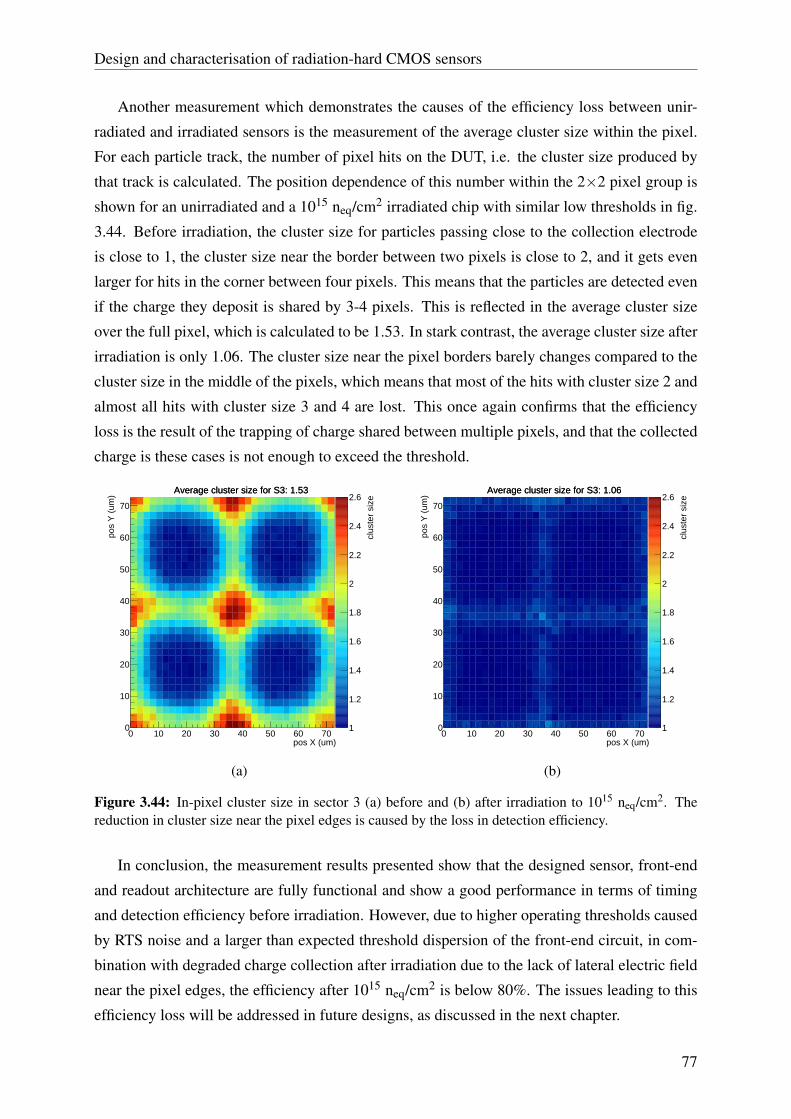
Design and characterisation of radiation-hard CMOS sensors
Another measurement which demonstrates the causes of the efficiency loss between unir-
radiated and irradiated sensors is the measurement of the average cluster size within the pixel.
For each particle track, the number of pixel hits on the DUT, i.e. the cluster size produced by
that track is calculated. The position dependence of this number within the 2×2 pixel group is
shown for an unirradiated and a 1015 neq/cm2 irradiated chip with similar low thresholds in fig.
3.44. Before irradiation, the cluster size for particles passing close to the collection electrode
is close to 1, the cluster size near the border between two pixels is close to 2, and it gets even
larger for hits in the corner between four pixels. This means that the particles are detected even
if the charge they deposit is shared by 3-4 pixels. This is reflected in the average cluster size
over the full pixel, which is calculated to be 1.53. In stark contrast, the average cluster size after
irradiation is only 1.06. The cluster size near the pixel borders barely changes compared to the
cluster size in the middle of the pixels, which means that most of the hits with cluster size 2 and
almost all hits with cluster size 3 and 4 are lost. This once again confirms that the efficiency
loss is the result of the trapping of charge shared between multiple pixels, and that the collected
charge is these cases is not enough to exceed the threshold.
1
1.2
1.4
1.6
1.8
2
2.2
2.4
2.6
clus
ter
size
Average cluster size for S3: 1.53
0 10 20 30 40 50 60 70 pos X (um)
0
10
20
30
40
50
60
70
pos
Y (
um) Average cluster size for S3: 1.53
(a)
1
1.2
1.4
1.6
1.8
2
2.2
2.4
2.6
clus
ter
size
Average cluster size for S3: 1.06
0 10 20 30 40 50 60 70 pos X (um)
0
10
20
30
40
50
60
70
pos
Y (
um) Average cluster size for S3: 1.06
(b)
Figure 3.44: In-pixel cluster size in sector 3 (a) before and (b) after irradiation to 1015 neq/cm2. Thereduction in cluster size near the pixel edges is caused by the loss in detection efficiency.
In conclusion, the measurement results presented show that the designed sensor, front-end
and readout architecture are fully functional and show a good performance in terms of timing
and detection efficiency before irradiation. However, due to higher operating thresholds caused
by RTS noise and a larger than expected threshold dispersion of the front-end circuit, in com-
bination with degraded charge collection after irradiation due to the lack of lateral electric field
near the pixel edges, the efficiency after 1015 neq/cm2 is below 80%. The issues leading to this
efficiency loss will be addressed in future designs, as discussed in the next chapter.
77

Chapter 4
Optimisation of pixel matrix and readoutelectronics
4.1 Process improvements for radiation hardness
To improve the detection efficiency in the pixel corners after irradiation, two new process
changes have been developed to increase the lateral electric field at the pixel borders. The
idea is to introduce a junction along the sensor depth near the edge of the pixel, which would
enhance the lateral component of the electric field. This can be achieved by introducing an
additional extra-deep p-well implant near the pixels edges or by creating a gap in the n− im-
plant. The cross-sections of a pixel as well as a top view of the layout of 2×2 pixels for both
solutions are shown in fig. 4.1 and fig. 4.2, respectively. Apart from significantly increasing the
lateral field, both modifications shift the minimum of the electric field deeper into the silicon
compared to the original modified process. As a result, the electric field already starts to bend
towards the collection electrodes deeper within the silicon, reducing the drift path and hence the
charge collection time [79].
LOW DOSE N-TYPE IMPLANT
NWELL COLLECTION ELECTRODE
PWELLDEEP PWELL
P- EPITAXIAL LAYER
P+ SUBSTRATE
NWELL PWELL NWELLDEEP PWELL
PMOSNMOS
EXTRA DEEP PWELL EXTRA DEEP PWELL
(a)
Pixel matrix process splits
8CMOS demonstrator meeting – 17/9/2018
❶ additional “extra-deep p-well” layer
❷ gap in the n- layer
• layer already exists in standard TJ180 process: no process R&D needed
• requires only a change of the existing mask for the n-layer
collection electrode
n- layer
extra deep p-well
collection electrode
n- layer
(b)
Figure 4.1: Process modification with an additional extra-deep p-well near the pixel edges: (a) cross-section of a pixel, (b) top view of the modified layers in 2×2 pixels.
78

Optimisation of pixel matrix and readout electronics
LOW DOSE N-TYPE IMPLANT
NWELL COLLECTION ELECTRODE
PWELLDEEP PWELL
P- EPITAXIAL LAYER
P+ SUBSTRATE
NWELL PWELL NWELLDEEP PWELL
PMOSNMOS
(a)
Pixel matrix process splits
8CMOS demonstrator meeting – 17/9/2018
❶ additional “extra-deep p-well” layer
❷ gap in the n- layer
• layer already exists in standard TJ180 process: no process R&D needed
• requires only a change of the existing mask for the n-layer
collection electrode
n- layer
extra deep p-well
collection electrode
n- layer
(b)
Figure 4.2: Process modification with a gap in the n− layer near the pixel edges: (a) cross-section of apixel, (b) top view of the modified layers in 2×2 pixels.
Transient three-dimensional TCAD simulations have been performed for both modifications
to assess the improvements in charge collection time and collected charge after irradiation. The
traversal of a minimum ionising particle (MIP) is simulated at the corner of the 36.4×36.4 µm2
pixel, which is the worst case in terms of charge collection. To model the effects of radiation
damage, defect levels are introduced in the silicon bulk according to [80]. The voltage on the
collection electrode is set to 0.8 V, which is around the voltage needed for the correct operation
of the first stage of the front-end amplifier, while the p-wells and the substrate are biased at−6 V.
The transient evolution of the electrode current for the two new modifications and the original
modified process is shown in fig. 4.3a. Both proposed modifications provide a reduction in
charge collection time by at least a factor of two. By integrating the electrode current over time
one obtains the total collected charge. For the original modified process, a large fraction of the
Integration time [ns]5 10 15 20 25 30
Modified process
Gap in n-layer
Additional implant
ATLAS CMOS Meeting, 16.09.2018, Magdalena Munker, [email protected] !17
Transient results for irradiated sensors
• Charge collection time and signal after irradiation significantly improved for both new concepts
Current pulse for different sensor layouts: ifferent sensor layouts:
Particle incident at 1 nsPixel size of 36.4 μm x 36.4 μm
- 6 V
Pixel size of 36.4 μm x 36.4 μm- 6 V
CLICdp Work in Progress
Low n-layer dose
Low n-layer dose
(Reminder: simulation of worst case of particle incident at lateral position of field minimum)
(a)
Integration time [ns]0 5 10 15 20 25 30
]- [e
sing
le p
ixel
Q
0
100
200
300
400
Modified process
Gap in n-layer
Additional implant
ATLAS CMOS Meeting, 16.09.2018, Magdalena Munker, [email protected] !17
Transient results for irradiated sensors
• Charge collection time and signal after irradiation significantly improved for both new concepts
Current pulse for differ Charge for different sensor layouts:
ParticlPixel size of 36
Pixel size of 36.4 μm x 36.4 μm - 6 V
Low n-layer dose
(Reminder: simulation of worst case of particle incident at lateral position of field minimum)
(b)
Figure 4.3: TCAD simulations for (a) electrode current and (b) charge collected for a MIP incident atthe pixel corner after irradiation with different sensor layouts. Both new concepts show an improvedcharge collection time and higher collected charge [79].
79

Optimisation of pixel matrix and readout electronics
charge, which is above 300 e− before irradiation, is lost due to the trapping of charge carriers
in the low-field regions. For the new modifications, a fraction of the charge is still lost, but the
total collected charge is at least a factor of three higher than with the original modified process.
Using these simulations, the optimal width of the additional extra-deep p-well in the case of the
first modification (the green area in fig. 4.1b) for a pixel pitch of 36.4 µm is found to be 2.5 µm
for each pixel. Conversely, the optimal width of the gap in the n− implant in the case of the
second modification (the white area near the pixel borders in fig. 4.2b) is found to be 2 µm per
pixel.
Note that both improvements reduce the potential barrier between the p-wells and the sub-
strate provided by the n− layer. As a result, punchthrough will occur at lower substrate voltages
than in the original modified process. With a p-well voltage of −6 V, for the gap in the n− im-
plant the simulated substrate voltage at which punchthrough starts to occur is only around−8 V,
while for the additional extra-deep p-well this value is simulated to be around−10 V. However,
as evidenced by the MALTA efficiency measurements, increasing the substrate voltage beyond
those values does not result in better charge collection, so the optimal substrate voltage for the
new modifications is in any case in the range achievable before the onset of punchthrough. Also
note that both improvements require only a minimal change in the manufacturing process. In
the case of the gap in the n− layer, only a mask change for the n− implant is required, while
for the additional extra-deep p-well, one additional mask is required, but this implant is already
available in the foundry, so no process development is needed.
4.2 Pixel matrix design changes
The new process modifications have been included in a small-scale redesign of the MALTA
pixel matrix, which is part of a new test-chip called miniMALTA. The new matrix is 16 (columns)
by 64 (rows) large, and contains only the "medium" deep p-well variation of the sensor layout,
which has proven beneficial for the charge collection. Horizontally, it is divided into four sec-
tors: one with PMOS reset and the original modified process and three with diode reset and
the three process variations: original modified process, additional extra-deep p-well and gap
in the n− layer. Vertically, it is divided into two sectors with different front-end designs. The
left side contains a front-end modified by enlarging two front-end transistors, most importantly
M3, in order to reduce RTS noise. The W/L ratio of M3 has been increased from 1/0.18 µm to
1.22/0.38 µm, which was a simple layout change increasing the area of said transistor by more
than a factor of two. The change also provides a decrease in the output conductance of M3 and
an increase in front-end gain, which is simulated to be around 30% higher, with only a slight
penalty on the transconductance of M3 and the capacitance on OUTA. The size of the clipping
transistor M4 has also been increased for better control of the clipping threshold. The right
80

Optimisation of pixel matrix and readout electronics
side of the matrix contains the original MALTA front-end for comparison. In terms of readout
architecture, the matrix is the same as the MALTA design: only the four groups of 2×8 pixels
with the highest group addresses of both "colours" have been included, resulting in the 64 row
height.
The layout of the full miniMALTA chip is shown in fig. 4.4. Apart from the changes in the
pixel matrix, miniMALTA contains several new features at the chip periphery. A new readout
logic is included at the end-of-column to synchronise the asynchronous signals coming from
the matrix. After synchronisation, the hit data is read out synchronously with a clock frequency
of up to 640 MHz. This is done to simplify the design of the digital periphery after problems
with the asynchronous merger logic, but also to enhance compatibility with the off-chip readout
systems typically used in the experiments, while maintaining a low digital power consumption
in the matrix. A new design of the configuring logic (labelled "slow control"), which was
not working reliably in MALTA, has also been included. The DACs have been modified to
use 8 bits and to be more modular and independent of the matrix size (the previous design
implemented in MALTA was a single block occupying the full width of 512 pixels). Finally,
the data transmission unit (DTU) used in the ALPIDE chip was added to send the serialised hit
data off-chip using a single LVDS output transmitting the data at 1.2 Gb/s with double data rate
(DDR). The 600 MHz needed for this transmission is also generated inside the DTU using a
phase-locked loop (PLL).
Layout 5 mm x 1.77 mm
5CMOS demonstrator meeting – 17/9/2018
Pixel matrix
Slow Control
Sync FIFO & RO
DACs
Clock Receiver
LVDS 1.2 Gb/s, PLL LVDS 40 Mb/s
Figure 4.4: Layout of the 5×1.7 mm2 miniMALTA chip.
4.3 Synchronisation at the end-of-column
4.3.1 Random-access memory for synchronisation
The basic idea of the synchronisation circuitry at the end-of-column is to use the reference
signal to store the asynchronous pixel and group address signals into a random-access memory
(RAM). Since the pulses on the address lines are aligned in time with the reference signal, the
latter can be used to enable the writing into the RAM cells, resulting in a logic one being written
81

Optimisation of pixel matrix and readout electronics
if there is a pulse on a certain address line or a logic zero being written in the absence of a pulse.
Each of the two 22-bit buses in a double column (one for the "blue" groups and one for the "red"
groups) are connected to their own synchronisation block, so the total number of these blocks
is two per double column. Apart from the pixel and group address data, the reference signal
also stores a timestamp by storing the values of two counters: a 3-bit BCID counter running at
40 MHz and a 4-bit fine time counter running at 640 MHz. This means that the time of arrival of
the pulses from the matrix can be recorded with a precision of one 640 MHz clock cycle, which
is around 1.5 ns. As already mentioned, this can be useful to obtain some information about
the charge collected by pixels in a cluster. In the case of multiple consecutive pulses on one
reference line, up to four data words can be stored in four rows of the RAM memory. Hence,
each synchronisation block contains 28×4 RAM cells, as visualised in fig. 4.5.Synchronisation at the end-of-column
2222
16b pixel address5b group addressreference
640 MHzfine time counter
40 MHzBCID
counter
22
28x4 bits
Figure 4.5: Working principle of the synchronisation memory in miniMALTA. The 22 address bits andadditional timestaps are stored in a 28x4 RAM memory.
The basic building block of the RAM memories is the standard dual-port RAM cell with 8
transistors depicted in fig. 4.6. This cell consists of two cross-coupled inverters (transistors M0-
M4) and two sets of two NMOS pass transistors used for writing and reading. The writing is
done using M4 and M6, which force the the values of DATAIN and its complement DATAINB to
be stored at the outputs of the two inverters in feedback when the reference signal REF is active.
The memory cell is read out when a read signal is applied to the gates of M5 and M7, forcing the
value of DATAOUT to the value of DATAIN previously stored. Note that because only NMOS
pass transistors are used to save space, the signals will not achieve a full swing of 1.8 V on
DATAOUT , but will go up to∼1.2 V determined by the threshold voltage of the NMOS devices.
However, the quick transition between 0 and 1.2 V because of the small size of the memory
and low capacitance of the data lines allows a simple inverter on the complementary data output
DATAOUT B to be used to restore the full-swing data signal on OUT . Therefore, when the READ
82

Optimisation of pixel matrix and readout electronics
signal is active, the previously stored DATAIN will be asserted to the OUT node of the memory
cell. The DATAIN and DATAOUT lines are in common for the four rows of the RAM memory,
but the use of a dual-port cell enables the simultaneous writing and reading of different rows
within the memory.
Figure 4.6: Schematic of the standard dual port RAM cell used as the basic memory element. An inverteris enough to convert the RAM data output signal to a full-swing digital pulse.
The way the RAM cells and the synchronisation blocks are organised within the layout of
two double columns is shown in fig. 4.7. The four synchronisation blocks, two for the "blue"
groups and two for the "red" groups of the two double columns are placed one above the other,
taking up a total width of four columns (145.6 µm) and a height of only 157.3 µm. Each syn-
chronisation block contains the full-custom layout of the 28×4 RAM cells and the addressing
logic needed to point to the correct rows for writing and reading, which was synthesised and
laid out using digital place-and-route tools. The routing structure connecting the matrix signals
to the inputs of the RAM again has a balanced capacitive load, and additional buffers and delay
gates are added to the address lines to ensure that a timing misalignment of up to ∼400 ps with
respect to the reference signal still results in the correct writing of the RAM cells.
4.3.2 Peripheral readout logic
The READ signal used to read out the data from the synchronisation memories is generated
by the synchronous peripheral readout logic. This logic is designed to operate with the fast
640 MHz clock also used for storing the fine timestamp in the RAM cells. A block diagram of
the readout logic is shown in fig. 4.8. When a data word is stored in one of the synchronisation
memories, a signal is sent to the priority encoder logic denoting that a hit has been detected. The
priority encoder then sends the READ signal to the corresponding memory. The data word from
that memory is then transferred to a larger first-in-first-out (FIFO) memory, which is a standard
clocked RAM memory with a depth of 64 words provided by the foundry. In the process, 4
double-column identifier bits are added to the 28-bit data word, as well as additional BCID
83

Optimisation of pixel matrix and readout electronicsSynchro
sync. block 1sync. block 2sync. block 3sync. block 4
… …
22222222
145.6 µm
157.3 µm
RAM 1
buffers 1addressing & circuitry 1
RAM 2
buffers 2addressing & circuitry 2
RAM 3
buffers 3addressing & circuitry 3
RAM 4
buffers 4addressing & circuitry 4
Figure 4.7: The organisation and layout of 4 synchronisation memories and the surrounding logic.
timestamping bits to allow the storage of the data word for a longer time without losing timing
information, resulting in a 48-bit length of the data word. If there are multiple hits stored in
the synchronisation memories, the priority encoder will give priority to the reading out of the
leftmost memory (memory 0). The decision on which memory has the priority and the process
of transferring hits from that memory to the large FIFO takes three 640 MHz clock cycles.
With this kind of readout rate, simulations show that a synchronisation memory depth of four
is enough to have negligible hit losses with the expected hit rates. The value of three bits for
assigning the BCID timestamp during synchronisation also comes from the fact that, with the
readout rates in question, eight 25 ns clock cycles are enough to read out the synchronised data
in all cases.
0 1 2 3 … x16
sync. mem.
priority encoder
TJ RAM FIFO
8b/10b encoder … x6
ALPIDE serialiser + driver
shift register
LAPA driver
if SLOW=1
21b addr.
4b timing
3b BCID
28b + 4b col. ID + additional BCID
48b
60b @20 MHz
@1.2 Gbit/s
@40 MHz
Figure 4.8: Block diagram of the logic used to read out the 16 synchronisation memories.
Once the data word is stored in the FIFO, it is read out in two 40 MHz clock cycles and sent
to an 8b/10b encoder. This kind of encoding is commonly used to achieve a DC balanced code
84

Optimisation of pixel matrix and readout electronics
when the resulting data word is serialised (the average number of zeros and ones transmitted is
equal). This gives the possibility to AC couple the chip output to the readout systems, which is
typically done in the experiments. Six 8b/10b encoders are used to encode the 48-bit data word
into the final 60-bit data word. The parallel 60 bits are then fed to the ALPIDE data transmission
unit, which serialises the bits and transmits them off-chip through a single LVDS data output at
1.2 Gb/s, using double data rate and a 600 MHz clock generated by the internal PLL.
As a backup feature, a so-called "slow" readout option has also been included in the periph-
eral readout logic. If this mode is enabled, the 48-bit data word at the output of the FIFO is
directly serialised using a shift register with a slow clock of 40 MHz. This means that the time
to transmit the serialised data is 48× 25 ns = 1.2 µs, which is a factor of 24 slower than the
"fast" readout using the ALPIDE DTU. In this case, the data is transmitted off-chip using the
LAPA LVDS driver, already implemented and tested in MALTA. This mode of operation limits
the maximum output bandwidth and readout rate of the chip, but preserves all the address and
timing information, and provides a functionality equal to the "fast" readout for sufficiently low
particle hit rates.
4.4 Test results before and after irradiation
As was the case with MALTA, the fabricated miniMALTA chips are wirebonded to a PCB and
read out with an FPGA, this time a Kintex KC705. One of the first tests performed is a DAC
linearity scan, not only to test the performance of the redesigned DACs, but also to check the
operation of the new configuring logic. The DAC currents and voltages are monitored by con-
necting a source meter to the DAC monitoring pads of the chip. The measured current and
voltage values for different codes of a current DAC (IT HR) and a voltage DAC (VHIGH) are
shown in fig. 4.9. Both DACs show an excellent linearity, which is within 0.6%. The same
79/4/2019
0 50 100 150 200 250DAC code
0.05-
0.04-
0.03-
0.02-
0.01-
0
3-10´
curre
nt S
C_I
THR
IDAC monitoring
(a)69/4/2019
0 50 100 150 200 250DAC code
0.2
0.4
0.6
0.8
1
1.2
1.4
1.6
1.8
volta
ge S
C_V
PULS
E_H
VDAC monitoring
(b)
Figure 4.9: Linearity plots for (a) current DACs and (b) voltage DACs in the miniMALTA chip. In bothcases the integral nonlinearity is below 0.6%.
85

Optimisation of pixel matrix and readout electronics
plots have also been produced for the DACs on chips which had received up to 90 Mrad of
TID. Apart from a slight decrease in the range of the current DACs, as expected from the TID-
induced threshold voltage increase of the PMOS transistor generating the reference current,
the functionality and linearity of the DACs remains within the same values as before irradia-
tion. This confirms that the DACs and the digital logic used to configure them operate without
problems even after irradiation.
The next step is to test the front-end performance of unirradiated devices, in particular to
compare the two different front-end designs implemented on the chip. Again, this can be done
by placing an 55Fe source over the pixels where the analogue output of the front-end amplifier
can be monitored and comparing the resulting amplitude distributions. For this and all further
measurements, the p-well voltage is set to −2 V, since it could not be increased to higher
absolute values because the source/drain of a decoupling capacitor was mistakenly connected
to this voltage, causing a breakdown of the gate oxide for the usual value of −6 V. However,
already at −2 V of p-well bias, the n− implant around the collection electrode is depleted,
so a small capacitance and a near-maximal amplifier output signal are already achieved. The
substrate is biased at −6 V, and no signs of punchthrough between p-well and substrate are
observed. Both monitored pixels use the original modified process without any of the new
process improvements.
As expected, for the same DAC settings the front-end with the enlarged transistors M3 and
M4 exhibits a higher gain, resulting in the K-α peak in the 55Fe spectrum shifted towards higher
amplitudes, as seen in fig. 4.10. However, the difference in the peak amplitude and hence a
150 200 250 300 350 400 450 500 550 600 650
amplitude (mV)
0
50
100
150
200
250
num
ber
of h
its
55Fe spectra from amplifier output
enlarged transistorsstandard transistors
7 = 304.5 mV< = 4.9 mV
7 = 523.9 mV< = 7.4 mV7 = 523.9 mV< = 7.4 mV
Figure 4.10: Comparison of 55Fe spectra obtained from the monitored amplifier outputs in the sectorswith enlarged and standard transistors.
86

Optimisation of pixel matrix and readout electronics
difference in gain of a factor of 1.7 is significantly higher than expected from simulations. This
has raised some questions on the modelling of the output conductance of the devices, especially
with reverse p-well bias and BSIM simulation models, which are being discussed with the
foundry. Nevertheless, this significant gain increase makes it easier to achieve the desired low
thresholds with the modified front-end. Note that the spectrum in the front-end with standard
transistors is not to be compared with the spectra obtained from MALTA shown in the previous
sections, since the front-end settings had to be adjusted to avoid saturating the OUTA signal in
the sector with enlarged transistors for the maximum charge deposited by the 55Fe source (IT HR
had to be set to a high DAC code of 127).
The gain difference of a factor of 1.7 is confirmed by a threshold difference of a factor of
1.8 between the two front-end flavours, as seen in the threshold scans over the full matrix in
fig. 4.11a. Again, the scan is performed using the pulse injection circuitry and by sweeping the
value of VLOW , obtaining the S-curves and converting the threshold value to electrons. The scan
is performed at a temperature of−20C to be able to directly compare the threshold values with
those of irradiated chips later on. Note that the temperature has quite an impact on the threshold,
which decreases at lower temperatures, mainly due to an increase in the transconductance of the
discriminator input transistor M9. Apart from the threshold difference between the two sectors,
the threshold dispersion of the sector with enlarged transistors (sector 1, red curve) is also a
factor of 2 lower than for the original front-end, since for a constant discriminator threshold the
mismatch scales approximately with the charge threshold of the front-end. The relatively high
thresholds in both sectors are a result of setting the discriminator threshold to a high value (IDB
DAC code of 100). Another interesting difference to observe between the two designs is the
noise distribution shown in fig. 4.11b. The two sectors show a similar mean noise value, but the
reduction in the number of pixels in the noise tail for the enlarged transistor sector is striking,
resulting in a smaller RMS value of the noise distribution. This confirms that the tail in the
49/4/20190 100 200 300 400 500 600 700
threshold [el]0
20
40
60
80
100
120
140
# pi
xels
Sec 1Entries 384Mean 263.2RMS 24.44
Sec 2Entries 382Mean 485.2RMS 50.9
(a)59/4/2019
0 5 10 15 20 25 30 35 40 45 50noise [el]
0
20
40
60
80
100
120
140
160
# pi
xels
Sec 1Entries 384Mean 11.0RMS 2.79
Sec 2Entries 382Mean 12.7RMS 4.6
(b)
Figure 4.11: (a) Threshold and (b) noise distributions for the two sectors of an unirradiated miniMALTAchip. The left side of the matrix (red sector) has a lower threshold due to a higher front-end gain.
87

Optimisation of pixel matrix and readout electronics
blue curve is indeed caused by random telegraph noise in transistor M3, and that increasing the
area of this device by more than a factor of 2 almost completely removes the excessively noisy
pixels, which is why the red curve resembles a Gaussian distribution much more.
Several miniMALTA chips have been irradiated with neutrons to NIEL fluences of 1015 neq/cm2
and 2×10¹⁵ neq/cm2. During irradiation, the chips have also received 1 Mrad and 2 Mrad of
TID dose, respectively. The performance of the sensor and analogue front-end can once again
be compared by acquiring 55Fe spectra from the monitored amplifier outputs. This comparison
is shown in fig. 4.12. All the amplitude distributions were obtained from pixels with enlarged
transistors and without any of the new process modifications. The p-well was biased at −2 V,
while the substrate was at a voltage of −6 V. The front-end settings were once again adjusted
to avoid saturating the analogue output in any of the samples, and are the same for all three
samples compared. An increase in the mean signal amplitude of the K-α peak by about a factor
of 1.2 is observed for the 1015 neq/cm2 sample compared to the unirradiated one. As mentioned
before, this is attributed to the decrease of the collection electrode capacitance after irradiation.
This has been confirmed by measuring the K-α peak amplitude on the collection electrodes
themselves. A new feature in miniMALTA are additional monitoring pixels which buffer the
voltage signal of the electrode itself, without amplification, and the monitored signal amplitudes
show the same factor of 1.2 difference. Since the source followers used to buffer the electrode
signals are designed for a gain close to 1, changes in the circuit can not explain an increase in
signal after irradiation. One can also observe that the sensor and front-end are fully functional
even after a fluence of 2×10¹⁵ neq/cm2. There is only a slight reduction in signal amplitude
50 100 150 200 250 300 350 400 450 500 550 600
amplitude (mV)
0
50
100
150
200
250
300
350
400
num
ber
of h
its
55Fe spectra from amplifier output before and after irradiation
unirradiatedirradiated 1e15 neq/cm2, 1 Mradirradiated 2e15 neq/cm2, 2 Mrad
Figure 4.12: Comparison of 55Fe spectra obtained from the monitored amplifier outputs before and afterneutron irradiation.
88

Optimisation of pixel matrix and readout electronics
compared to the 1015 neq/cm2 irradiated sample, which is attributed to a slight decrease in the
front-end gain after TID. Nevertheless, the peak amplitude is still higher than before irradiation.
The energy resolution is degraded to the point where it is difficult to resolve the K-α from the
K-β peak of the 55Fe source, which is due to the noise increase also observed in MALTA.
The threshold and noise distributions of a chip irradiated to 1015 neq/cm2 are shown in fig.
4.13. These are directly comparable to the distributions for the unirradiated chip shown in fig.
4.11, since the threshold scans were performed in the same conditions and with the same front-
end settings. A decrease in threshold by a factor of 1.4 in both sectors is observed compared to
the unirradiated samples. This is partly because of the decrease in input capacitance, but also
because of a threshold decrease with TID due to a threshold voltage decrease in M9. The RMS
threshold variation is similar to the unirradiated chips, so the ratio between mean threshold and
RMS is somewhat degraded, but not the extent observed in MALTA. The mean noise values
show a slight increase after irradiation, and the RTS noise tail, especially in the sector with
the original front-end transistor sizes (blue curve), becomes much more prominent. A slight
tail can now also be observed in the enlarged transistor sector, so increasing the size of M3
to even higher values in future designs will help to completely suppress RTS noise even after
irradiation. Nonetheless, one can conclude that the new front-end with enlarged transistors
provides a significant improvement compared to the MALTA front-end by increasing the gain,
reducing the operating threshold and thereby the threshold dispersion, while almost completely
eliminating RTS noise.
89/4/2019 CMOS demonstrator meeting – [email protected] 100 200 300 400 500 600 700
threshold [el]0
20
40
60
80
100
120
140
# pi
xels
Sec 1Entries 383Mean 184.9RMS 27.08
Sec 2Entries 379Mean 342.8RMS 45.8
(a)99/4/2019 CMOS demonstrator meeting – [email protected]
0 5 10 15 20 25 30 35 40 45 50noise [el]
0
20
40
60
80
100
120
140
160
# pi
xels
Sec 1Entries 383Mean 13.3RMS 2.89
Sec 2Entries 379Mean 15.5RMS 5.4
(b)
Figure 4.13: Threshold and noise distributions for the two sectors of a miniMALTA chip irradiated withneutrons to 1015 neq/cm2.
To assess the improvement in charge collection brought about by the new process modifi-
cations before measuring the detection efficiency in beam tests, one can acquire data from a90Sr source and compare the hit occupancies in sectors with different process changes. The
difference in threshold between the two front-ends also has an impact on the occupancy, since
more hits are likely to be detected at lower thresholds. The source is placed over the chip in a
89

Optimisation of pixel matrix and readout electronics
way that it provides a close to uniform illumination of all sectors. The hit occupancies in all the
sectors are uniform before irradiation, which is expected, since the detection efficiency of even
the sector with a higher threshold and no process improvements is close to 100%, as seen from
beam test results on unirradiated MALTAs. However, after irradiation, the hit rates show a very
significant sector dependence, as seen in fig. 4.14. The most interesting comparison is between
sectors in the bottom half of the chip, since the gradient of the source illumination should be
negligible over such a small area. It is clear that the bottom quarter of the chip, which con-
tains the sectors with the original modified process, sees a considerably smaller number of hits
than the sectors above it, which include the additional extra-deep p-well near the pixel edges.
The ratio between the number of hits in the sector with enlarged transistors (left hand side) and
extra-deep p-well and the sector with the original transistors (right side) and original modified
process is about 100/60, which is consistent with the efficiency results obtained from irradiated
MALTA chips at these thresholds. The sectors with the gap in the n− layer on top of the chip
show an even higher occupancy, which could be due to the source gradient and a few pixels with
excessive noise rates which have not been masked. Note that to obtain this hit occupancy map,
several noisy pixels on the right side had to be masked, while on the left side no pixels were
masked at all. This is another confirmation that the enlarged M3 on the left side significantly
reduces the RTS noise hit rates, since even with a lower threshold the number of noisy pixels is
smaller. Also note that due to a problem in the biasing of the PMOS reset transistor, two sectors
of the chip are disabled, resulting in no hits between rows 32 and 47.
0 2 4 6 8 10 12 14x
0
10
20
30
40
50
60
y
IDB_140Entries 70735
0
20
40
60
80
100
120
140
160
180
coun
ts
IDB_140Entries 70735
Hit Occupancy
enlarged transistors standard transistors
PMOS reset
n- gap
extra-deep p-well
modified process
Figure 4.14: Hit occupancy over the full matrix during a 90Sr source acquisition after neutron irradiationto 1015 neq/cm2. The sectors with lower threshold and process modifications show the highest occupancy.
Apart from the difference in hit occupancy, the new process modifications should also affect
the average number of hits in a cluster. Since the electric field in both the sensors with the extra-
90

Optimisation of pixel matrix and readout electronics
deep p-well and the n− gap directs the charge more towards the electrode, a smaller average
cluster size is expected. This is proven to be true for unirradiated samples, where the cluster size
for a 90Sr source on the left side of the chip goes from 1.67 in the original modified process to 1.6
in the sectors with the gap in the n− layer. However, in samples irradiated to 1015 neq/cm2, the
trend is reversed and the original modified process has an average cluster size of 1.1, while both
process improvements show a cluster size of 1.15. The reason for this is the loss of efficiency
near the pixel edges in the original modified process. If charge is shared between multiple
pixels, in most cases the particle is not detected at all, so hits with large cluster sizes are not seen,
resulting in a reduced average cluster size for the original modified process. The reduction in
cluster size for the two process improvements is still significant, but the fact that it stays higher
than for the original modified process is already an indication of improved detection efficiency
near the pixel boundaries. The cluster size distributions as well as the cluster occupancies for
data from this 90Sr source acquisition are plotted in fig. 4.15. The threshold in the sectors with
enlarged transistors is set to around 280 e−, while for the original front-end it is around 500 e−.
In all three process flavours the cluster occupancy is higher in the enlarged transistor sectors,
which means that there is a threshold dependence to the efficiency even with the new improved
0 10 20 30 40 50 600
2
4
6
8
10
12
14
16 h2ClusterCountEntries 482422Mean x 29.41Mean y 6.928Std Dev x 19.66Std Dev y 4.583
0
200
400
600
800
1000h2ClusterCount
Entries 482422Mean x 29.41Mean y 6.928Std Dev x 19.66Std Dev y 4.583
78548 106235 10 90820
59945 79226 13 67625
cluster count
enla
rged
tra
nsis
tors
stan
dard
tra
nsis
tors
modified process extra-deep p-well n- gap
(a)
h1ClusterSizeS0
Entries 91465
Mean 1.105
Std Dev 0.4841
0 2 4 6 8 10 12 14 160
10000
20000
30000
40000
50000
60000
70000
80000
h1ClusterSizeS0
Entries 91465
Mean 1.105
Std Dev 0.4841
sec. 0, MALTA, enl. tr.h1ClusterSizeS1Entries 127521
Mean 1.153
Std Dev 0.5841
0 2 4 6 8 10 12 14 160
20
40
60
80
100
120310× h1ClusterSizeS1
Entries 127521
Mean 1.153
Std Dev 0.5841
sec. 1, extra deep p-well, enl. trh1ClusterSizeS3
Entries 108247
Mean 1.152
Std Dev 0.5862
0 2 4 6 8 10 12 14 160
20
40
60
80
100
310× h1ClusterSizeS3
Entries 108247
Mean 1.152
Std Dev 0.5862
sec. 3, n-gap, enl. tr.
0 2 4 6 8 10 12 14 160
10000
20000
30000
40000
0 2 4 6 8 10 12 14 160
20
40
60
0 2 4 6 8 10 12 14 160
20
40
cluster size =1.105
cluster size =1.153
cluster size =1.152
(b)
Figure 4.15: (a) Cluster occupancy and (b) cluster size distribution for different sectors with enlargedtransistors in miniMALTA after 1015 neq/cm2.
91

Optimisation of pixel matrix and readout electronics
sensor layouts, because a fraction of the hits are lost a high threshold of 500 e−. However, the
difference between the extra-deep p-well sector and the original modified process sector with the
same threshold is equally striking, indicating that the process improvements themselves could
bring up to a factor of 1.35 increase in detection efficiency. Similar trends are also observed for
samples irradiated to 2×10¹⁵ neq/cm2, which confirms the new process modifications improve
the charge collection even after higher irradiation fluences.
Four miniMALTA chips have also been irradiated with protons in the irradiation facility
at the University of Birmingham [81]. Proton irradiations cause both NIEL and TID damage
and are useful to assess the combined effects of high NIEL fluences on the sensor and high
TID doses on the electronics. Once again, a comparison between the 55Fe spectra collected
from three chips is made, as shown in fig. 4.16. With the same front-end settings, a fac-
tor of 1.13 decrease in signal amplitude is observed after irradiation to 7×10¹³ neq/cm2 and
9.3 Mrad. With this non-ionising fluence the effect on the input capacitance is still negligible,
so a slight decrease in front-end gain due to TID causes this reduction in signal. However, after
5×10¹⁴ neq/cm2 and 66.5 Mrad the K-α peak shifts towards higher amplitudes, close to the
unirradiated values, which is likely due to a combination of decreasing input capacitance and
the front-end recovering after higher TID doses, as explained in sect. 2.4. The fact that the
RMS of the K-α peak after proton irradiation to 5×10¹⁴ neq/cm2 is very similar to the unirradi-
ated values is somewhat surprising, since after neutron irradiation to similar fluences the RMS
showed an increase of up to a factor of two. Therefore, further proton irradiations are planned
to confirm the findings in this measurement.
50 100 150 200 250 300 350 400 450 500 550 600
amplitude (mV)
0
50
100
150
200
250
300
350
400
450
500
num
ber
of h
its
55Fe spectra from amplifier output before and after irradiation
unirradiatedirradiated 7e13 neq/cm2, 9.3 Mradirradiated 5e14 neq/cm2, 66.5 Mrad
Figure 4.16: Comparison of 55Fe spectra obtained from the monitored amplifier outputs before and afterproton irradiation.
92

Optimisation of pixel matrix and readout electronics
Threshold scans have been performed on various chips for various levels of neutron and
proton irradiation to compare the effects of different types of irradiation. The measured mean
threshold values for different settings of the IDB DAC current are summarised in fig. 4.17. Table
4.1 shows which chip has been irradiated to which level and with what type of particles. As
already mentioned, the general trend is that for the same IDB value the threshold decreases both
with proton and neutron irradiation. Neutron irradiation seems to affect the threshold more
because of the decrease in electrode capacitance after a high NIEL fluence and a decrease in the
discriminator threshold due to TID. The effect on the discriminator threshold is the dominant
effect after proton irradiation and still causes a decrease in threshold, though not as significant as
50 100 150 200 250IDB
0
100
200
300
400
500
Thr
esho
ld [e
]
Left regionRight regionW1R9W2R9W4R9W5R3W4R2W5R11
ICASN_10 ITHR_20 IBIAS_120 -20C
Figure 4.17: Comparison of threshold versus IDB DAC value for an unirradiated, 2 neutron irradiatedand 3 proton irradiated miniMALTA chips.
Table 4.1: List of miniMALTA chips and the levels to which they have been irradiated.
Chip Irradiation type NIEL fluence (neq/cm2) TID dose (Mrad)
W5R11 none 0 0
W4R9 proton 7×10¹³ 9.3
W2R9 proton 5×10¹⁴ 66.5
W1R9 proton 7×10¹⁴ 91
W4R2 neutron 1×10¹⁵ 1
W5R3 neutron 2×10¹⁵ 2
93

Optimisation of pixel matrix and readout electronics
with high neutron fluences. Note that by varying other front-end DAC settings one can achieve
an even wider range of thresholds, and ultimately the only limiting factors as to how low one
can go with the charge threshold after irradiation are the noise and threshold dispersion.
The performance of the readout architecture, especially the newly implemented synchroni-
sation block has also been tested extensively. The previous measurements (threshold scans and
source acquisitions) already prove that the pixel address data is read out correctly and that the
asynchronous matrix signals can indeed be synchronised on-chip and read out using the syn-
chronous periphery logic. For these measurements, the "slow" readout mode, where the data is
serialised at 40 Mb/s, has been used. First measurements on the "fast" readout mode for high hit
rates indicate that this mode of operation also functions correctly, but the firmware development
for sampling the 1.2 Gb/s output signal is still ongoing.
An additional function of the synchronisation block is to add the 640 MHz fine time and
40 MHz BCID timestamps to the address words. An early test to check the validity of these
timing bits is to look at the distribution of the fine time and BCID values in the data acquired
while placing a 90Sr source over the chip. Since the timing of the particle hits is not correlated
with any of the clocks, a uniform distribution for both counters is expected. The measured
distributions for the BCID and fine time counter values are shown in fig. 4.18. The x-axis of
the plots gives the value of the 4-bit fine time counter and the 15-bit BCID counter (added in
the peripheral logic after synchronisation) values converted to a decimal number. Both distri-
butions are uniform to within ±10%. The slight non-uniformity stems from the fact that the
period of counters used to generate these timestamps is not exactly balanced, so each value of
the counter will have a slightly different duration than the others. In the case of the fine time,
the simulated timing difference between the values matches almost exactly the measured distri-
butions: a shorter duration for a given counter value results in less hits with that value within
the distribution. This is already a good indication that the timestamps are stored correctly and
that they can be used to obtain the time of arrival of hit signals to the periphery.
htempEntries 304913Mean 1.634e+04Std Dev 9455
0 5000 10000 15000 20000 25000 30000BCID
0
500
1000
1500
2000
2500
3000
3500htemp
Entries 304913Mean 1.634e+04Std Dev 9455
BCID counter distribution
(a)
htempEntries 304913Mean 7.479Std Dev 4.636
0 2 4 6 8 10 12 14 16fine time
0
2000
4000
6000
8000
10000
12000
14000
16000
18000
20000htemp
Entries 304913Mean 7.479Std Dev 4.636
Fine time counter distribution
(b)
Figure 4.18: Distribution of (a) BCID and (b) fine time counter values during a 90Sr source acquisition.Both distributions are uniform within ±10%.
94

Optimisation of pixel matrix and readout electronics
The 640 MHz clock used in the peripheral readout logic and for the fine time counter is
generated on the FPGA board and sent to the chip. Depending of the FMC cable connection
between the chip and the FPGA, the clock signal can be degraded to the point where some of
the data words coming from the chip do not contain the correct address information. Slowing
the clock down to 320 MHz solves these problems, so most of the following tests are performed
with this clock frequency. This implies a slower readout of the synchronisation memories,
which does not present any limitation for the hit rates used in source tests and beam tests.
It also implies that the resolution of the fine time counter is now one 320 MHz clock cycle,
so around 3 ns. With this in mind, one can use the timestamps to obtain information about the
timing difference of hits within clusters. An example for this is shown in fig. 4.19 for horizontal
clusters between two double columns, so hits in neighbouring pixels within the same row, but
in different groups of 2×8, therefore stored in different synchronisation memories. The hit data
was acquired during a beam test, and the hit position on the sensor can be obtained from the
beam telescope with a sub-pixel precision. When charge is shared equally among two pixels,
the timing difference is close to 0, since the two pixel front-ends respond at approximately the
same time. This happens if the charge is deposited very close to the boundary between the
pixels. Fig. 4.19b shows that these hits (the red squares between pixel 0 and 1) indeed result
in a timing difference of 0. As the hit position moves further away from the pixel edge, one
pixel will collect the majority of the charge, while the other will collect only a small amount,
so the average timing difference increases. As seen in fig. 4.19a, the vast majority of the hits
come with a timing difference of less than 50 ns, as expected from the time walk curve of the
amplifier. This confirms that the timing information from the counters is correct and that it can
be used to at least qualitatively estimate the charge deposited in pixels of a cluster. Note that, for
flexibility, the rising edges of two clocks used for timestamping (the 40 MHz and the 320 MHz)
are not synchronised on-chip, but can be synchronised on the FPGA with a precision of oneDeltaTforhorizontalclustersintwodifferentdoublecolumns
200− 150− 100− 50− 0 50 100 150 200 (ns)
0
200
400
600
800
1000
HorCluDeltaTDC
TiminginformationfromMini-MALTA 21
(a)
Horizontalclustersintwodifferentdoublecolumns
0 0.2 0.4 0.6 0.8 1 1.2 1.4 1.6 1.8 2Pixel X
40−
30−
20−
10−
0
10
20
30
40
Del
taT
(ns)
0
50
100
150
200
250
Horizontal Clusters of size 2 in different double columns
TiminginformationfromMini-MALTA 22
q AverageDeltaTineachbinvstrackpositionshowsacleartrend(b)
Figure 4.19: (a) Distribution of the timing difference between two pixels in a horizontal cluster betweentwo double columns during a beam test and (b) the same timing difference versus hit position within thepixel.
95

Optimisation of pixel matrix and readout electronics
320 MHz clock cycle. This still leaves a slight misalignment between the clocks, resulting in
the fact that hits arriving close to the rising edge of the 40 MHz clock, within this misalignment
window, can not be assigned the correct timing information in the offline analysis. This is why
a small fraction of hits in the timing distribution is assigned the wrong delay value (around ±150 ns). This can easily be solved by dividing the frequency of the fast clock on-chip and using
this clock to generate the BCID counter value, which will probably be the case in future designs.
As was the case with MALTA, the detection efficiency of miniMALTA chips before and
after irradiation has been measured in beam tests. Beam test campaigns have been carried out
at the German Electron Synchrotron (DESY) and the ELSA electron accelerator in Bonn. The
following results are taken from the beam tests at ELSA, where the miniMALTA (the DUT) and
the beam telescope are placed in a 2.5 GeV electron beam. The six telescope planes used in these
tests were actually unirradiated MALTA sensors, which provide a good position resolution for
tracks on the DUT surface thanks to the small pixel size. However, the resolution is somewhat
degraded due to multiple scattering effects caused by the low-energy electron beam, so the best
resolution one can achieve is around 13 µm. This limits the amount of in-pixel efficiency studies
that can be performed, but is more than enough to determine the overall efficiency for different
sectors of the miniMALTA chip. The reconstructed tracks are matched to hits from the DUT
after applying a timing cut, and the efficiency is once again calculated as the number of matched
tracks over the total number of reconstructed tracks.
The efficiency plots for an unirradiated miniMALTA sample with a 30 µm thick epitaxial
layer are shown in fig. 4.20a. The IDB DAC setting of 20 results in a threshold of around
200 e− in sectors on the left-hand side and 380 e− on the right-hand side. The p-well and the
substrate are biased at −2 V and −6 V, respectively. Pixels in the bottom right sector, which
are identical to the MALTA design, show an efficiency of 98%, which matches the highest
efficiency numbers measured on unirradiated MALTA chips. The process improvements in
the sectors above increase the efficiency by an additional percent, while the combination of
process improvements and low thresholds on the left-hand side brings the detection efficiency
up to 99.8% in the sector with additional extra-deep p-well. This demonstrates that the process
changes improve the charge collection even before irradiation, and that at low enough thresholds
the sensor is fully efficient. Fig. 4.20b shown the detection efficiency measured for a sample
irradiated with neutrons to 1015 neq/cm2. During the measurement, the chip was cooled down
to −20C. The IDB setting of 100 corresponds to a threshold of 200 e− and 340 e− on the left
and right side of the chip, respectively. Looking at the bottom right sector identical to MALTA,
the efficiency of 78.8% again matches the highest values measured in MALTA beam tests quite
well. The process improvements bring a significant efficiency increase of nearly 10%, even
with the relatively high threshold of 340 e− on the right side. With lower thresholds obtained
on the left side of the chip, the efficiency reaches an impressive 97.9% in the sector with the
96

Optimisation of pixel matrix and readout electronics
Revisiting proton-irradiated chips + selection of plots for the paper5 June 2019
W2R11: re-analysis
24
0 2 4 6 8 10 12 14 16Pixels X
0
10
20
30
40
50
60Pi
xels
Y
80
82
84
86
88
90
92
94
96
98
100
Effic
ienc
y %
0.0±99.7
0.0±99.8
0.0±99.7
0.1±98.0
0.0±99.1
0.0±99.2
Efficiency per sectors in MiniMalta
0 2 4 6 8 10 12 14 16Pixels X
0
10
20
30
40
50
60
Pixe
ls Y
80
82
84
86
88
90
92
94
96
98
100
Effic
ienc
y %
0.0±99.6
0.0±99.9
0.0±99.7
0.1±98.3
0.1±99.0
0.1±99.2
Efficiency per sectors in MiniMalta
0 2 4 6 8 10 12 14 16Pixels X
0
10
20
30
40
50
60
Pixe
ls Y
80
82
84
86
88
90
92
94
96
98
100
Effic
ienc
y %
0.0±99.7
0.0±99.8
0.0±99.7
0.1±98.0
0.1±99.0
0.1±99.2
Efficiency per sectors in MiniMalta
IDB20_SUB6 IDB20_SUB2 IDB20_SUB10
masked pixel now accounted in fiducial volume definition
~200 el ~380 el ~200 el ~380 el(a)
50
55
60
65
70
75
80
85
90
95
100
eff.
(%)
0 2 4 6 8 10 12 14 16 PixX
0
10
20
30
40
50
60 Pix
Y
0 2 4 6 8 10 12 14 16Pixels X
0
10
20
30
40
50
60
Pixe
ls Y
50
55
60
65
70
75
80
85
90
95
100
Effic
ienc
y %
0.1±91.9
0.1±97.9
0.1±97.6
0.2±78.8
0.1±87.0
0.1±86.5
Efficiency per sectors in MiniMalta
0 2 4 6 8 10 12 14 16Pixels X
0
10
20
30
40
50
60
Pixe
ls Y
50
55
60
65
70
75
80
85
90
95
100
Effic
ienc
y %
0.2±92.0
0.1±97.9
0.1±97.6
0.2±78.7
0.2±87.0
0.2±86.6
Efficiency per sectors in MiniMalta
50
55
60
65
70
75
80
85
90
95
100
eff.
(%)
0 2 4 6 8 10 12 14 16 PixX
0
10
20
30
40
50
60 Pix
Y
50
55
60
65
70
75
80
85
90
95
100
eff.
(%)
0 2 4 6 8 10 12 14 16 PixX
0
10
20
30
40
50
60 Pix
Y
0 2 4 6 8 10 12 14 16Pixels X
0
10
20
30
40
50
60
Pixe
ls Y
50
55
60
65
70
75
80
85
90
95
100
Effic
ienc
y %
0.2±91.8
0.1±97.9
0.1±97.6
0.3±79.0
0.2±87.0
0.2±86.5
Efficiency per sectors in MiniMalta W2R1 (1e15): re-analysis
IDB100_SUB6
IDB100_SUB6
merging since compatibleno pixel mask offline
IDB100_SUB6
IDB100_SUB6
IDB100_SUB6
IDB100_SUB6
(b)
Figure 4.20: Efficiency in beam tests for different sectors of miniMALTA: (a) before irradiation, (b)after neutron irradiation to 1015 neq/cm2.
additional extra-deep p-well. The sectors with extra-deep p-well consistently give a slightly
higher efficiency than the sectors with the gap in the n− layer, indicating that the former process
improvement is the better in terms of charge collection from a 30 µm thick epitaxial layer.
A summary of efficiency measurements performed on two chips irradiated to 1015 neq/cm2
at different threshold settings is shown in fig. 4.21. The two chips differ between each other in
terms of the thickness of the epitaxial layer, which is either 25 or 30 µm, as well as the depth
of the n− layer, which was implanted at a different angle, using channelling for the former and
100 200 300 400 500 600Threshold [e]
50
55
60
65
70
75
80
85
90
95
100
Effi
cien
cy [%
]
Large trans.Large trans. + extra p-wellLarge trans. + n-gapStd trans.Std trans. + extra p-wellStd trans. + n-gap
)2 neq/cm1510×W2R1+W4R2 (1
m E
PI)
µW
4R2
(25
m E
PI)
µW
2R1
(30
Figure 4.21: Efficiency versus threshold after neutron irradiation to 1015 neq/cm2. The plot contains thecombined data obtained from both sides of two chips at different threshold settings.
97
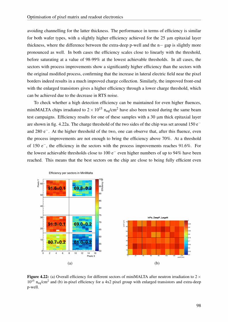
Optimisation of pixel matrix and readout electronics
avoiding channelling for the latter thickness. The performance in terms of efficiency is similar
for both wafer types, with a slightly higher efficiency achieved for the 25 µm epitaxial layer
thickness, where the difference between the extra-deep p-well and the n− gap is slightly more
pronounced as well. In both cases the efficiency scales close to linearly with the threshold,
before saturating at a value of 98-99% at the lowest achievable thresholds. In all cases, the
sectors with process improvements show a significantly higher efficiency than the sectors with
the original modified process, confirming that the increase in lateral electric field near the pixel
borders indeed results in a much improved charge collection. Similarly, the improved front-end
with the enlarged transistors gives a higher efficiency through a lower charge threshold, which
can be achieved due to the decrease in RTS noise.
To check whether a high detection efficiency can be maintained for even higher fluences,
miniMALTA chips irradiated to 2× 10¹⁵ neq/cm2 have also been tested during the same beam
test campaigns. Efficiency results for one of these samples with a 30 µm thick epitaxial layer
are shown in fig. 4.22a. The charge threshold of the two sides of the chip was set around 150 e−
and 280 e−. At the higher threshold of the two, one can observe that, after this fluence, even
the process improvements are not enough to bring the efficiency above 70%. At a threshold
of 150 e−, the efficiency in the sectors with the process improvements reaches 91.6%. For
the lowest achievable thresholds close to 100 e− even higher numbers of up to 94% have been
reached. This means that the best sectors on the chip are close to being fully efficient even
Revisiting proton-irradiated chips + selection of plots for the paper5 June 2019
0 2 4 6 8 10 12 14 16Pixels X
0
10
20
30
40
50
60
Pixe
ls Y
50
55
60
65
70
75
80
85
90
95
100
Effic
ienc
y %
0.4±71.7
0.3±82.6
0.3±82.5
0.4±50.1
0.4±52.2
0.4±52.8
Efficiency per sectors in MiniMalta
0 2 4 6 8 10 12 14 16Pixels X
0
10
20
30
40
50
60
Pixe
ls Y
50
55
60
65
70
75
80
85
90
95
100
Effic
ienc
y %
0.2±80.7
0.1±91.3
0.1±91.6
0.2±61.0
0.2±69.0
0.2±69.8
Efficiency per sectors in MiniMalta
SUB=10 V, changing threshold (via IDB)
W1R3 (2e15)
33
IDB=250
th=205e th=380e(a) Revisiting proton-irradiated chips + selection of plots for the paper5 June 2019
In-pixel plots (IDB=100)
W1R3 (2e15)
34
0.5
0.55
0.6
0.65
0.7
0.75
0.8
0.85
0.9
0.95
1
InPix_Malta_SmallN
0 20 40 60 80 100 120 140 m]µ posX [
0
10
20
30
40
50
60
70 m]
µ p
osY
[
InPix_Malta_SmallN
0.5
0.55
0.6
0.65
0.7
0.75
0.8
0.85
0.9
0.95
1
InPix_DeepP_LargeN
0 20 40 60 80 100 120 140 posX [µm]
0
10
20
30
40
50
60
70
pos
Y [µ
m]
InPix_DeepP_LargeN
(b)
Figure 4.22: (a) Overall efficiency for different sectors of miniMALTA after neutron irradiation to 2×10¹⁵ neq/cm2 and (b) in-pixel efficiency for a 4x2 pixel group with enlarged transistors and extra-deepp-well.
98

Optimisation of pixel matrix and readout electronics
after a fluence of 2× 10¹⁵ neq/cm2. Looking at the in-pixel efficiencies for the sector with
enlarged transistors and extra-deep p-well in fig. 4.22b, this time with a much coarser position
resolution than for the MALTA in-pixel plots, as explained earlier, one can still correlate the
slight efficiency loss in the best sectors with charge loss in the pixel corners. To further improve
the detection efficiency, one would need to work at thresholds even lower than 100 e− or use a
smaller pixel size with a redesigned front-end and readout logic to fit in the available area.
In conclusion, the improved front-end with increased gain and lower RTS noise imple-
mented in the miniMALTA chip allows operating the chip at low thresholds down to 100 e−.
At these thresholds and with the process modifications for improved charge collection near the
pixel edges, the sensors are practically fully efficient even after irradiation to 1015 neq/cm2. The
new digital periphery which synchronises the asynchronous signals form the pixel matrix has
proven to be an efficient and low-power way of reading out the chip while preserving accurate
timing information.
99

Chapter 5
Outlook for future design improvements
5.1 Further optimisation of analogue front-end circuitry
After the excellent results obtained with the miniMALTA sensors, design work is continuing
towards a new generation of large pixel matrices in TowerJazz 180 nm. Since the baseline
designs for the ATLAS pixel detector are still the hybrid solutions designed by the RD53 col-
laboration [82], new applications for large monolithic pixel sensors are also being investigated.
Further improvements on the front-end circuitry are being pursued in order to further reduce the
noise and threshold dispersion and achieve even lower operating thresholds, resulting in an even
higher detection efficiency after high irradiation fluences. Different approaches for the readout
of the large pixel matrices are also being investigated, either through an improved version of the
MALTA-like asynchronous readout optimised for smaller pixel sizes, or through a more con-
servative synchronous column-drain type of architecture. The submission of two large matrices
with all the improvements mentioned is planned for the end of 2019.
As far as the front-end design is concerned, a further increase in the area and output resis-
tance of the M3 NMOS current source would result in a further reduction of RTS noise after
irradiation and an even higher gain of the amplifier. A higher gain could also be beneficial for
the threshold mismatch, since the input-referred mismatch coming from the discriminator stage
is divided by the gain of the amplifier stage. Another way to significantly increase the gain is
to increase the size of the source capacitance CS, as explained in sect. 3.2.1. A re-layout of the
front end with the length of M3 increased by an additional factor of 2 compared to the enlarged
sectors of miniMALTA, as well as CS increased by nearly an additional factor of 7, has already
been included in a pixel size of 33.04×33.04 µm2. Note that a smaller pixel pitch than 36.4 µm
is preferred mainly due to the improvement in charge collection near the pixel edges and the
additional margin it provides in terms of the radiation hardness of the sensor.
100

Outlook for future design improvements
Even though an increased gain helps in reducing the mismatch contribution of the second
stage, measurements indicate that the dominant contribution is the threshold variation comes
from the gain dispersion itself, caused by the variation on the output conductance of M3. The
gain is defined by the total conductance seen from OUTA, which includes mainly the output con-
ductance of M3 and the transconductance of M6. For low IT HR settings which bring the highest
gain, the M3 output conductance dominates, and the variation on this causes a larger dispersion
than for high IT HR settings. Therefore, another potential improvement is to completely elimi-
nate the contribution of the M3 output conductance, which can be achieved by cascoding this
transistor. By adding a cascode M10, as shown in fig. 5.1, the conductance of the M3-M10
combination decreases by nearly two orders of magnitude. This also brings an additional in-
crease in gain. The node at the M10 source introduces an additional pole which deteriorates the
stability of the circuit, however, with a large CS capacitance a phase margin of above 60 can
still be achieved. Also, M10 can be made narrow and long for reduced capacitance on OUTA,
while M3 can be somewhat wider for a higher gm.
Figure 5.1: Transistors connecting to the OUTA node in the front-end design with cascoded M3 (M10 isthe cascode transistor).
An additional change in fig. 5.1 is that the M2 cascode is now biased by a DAC voltage
VCASP to have more margin with the saturation of transistors above it. Also note that the grounds
of the main branch of the amplifier (node NV SS) and the discriminator ground (AV SS) have
been split. In times of high hit activity, when multiple discriminators are firing and consuming
significant current, a common ground could mean a transient voltage increase on the source
of M3 in case the resistance of the ground connection is not negligible, resulting in a voltage
signal on OUTA which could lead to fake hits. This phenomenon is completely avoided if the
two grounds are connected to different ground lines which are only connected together at the
pad level or on the PCB.
101

Outlook for future design improvements
A simulation comparing the transient response of the miniMALTA front-end with enlarged
M3 and the newly designed front-end with cascoded M3 for an input charge of 200 e− is shown
in fig. 5.2. With the same front-end settings, adjusted for the miniMALTA front-end to have a
threshold of around 200 e−, the new design exhibits a factor of 3 higher gain, which makes any
mismatch contribution from the second stage negligible when referred back to the input. Note
that the front-end biases need to be adjusted to achieve the desired threshold with the cascoded
front-end (IT HR has to be increased to have a threshold sufficiently higher than the noise levels,
around 100 e−). Also note that, in the simulation, the gate voltage of the clipping transistor has
been adjusted for a discriminator pulse width which is still within the simulation window. By
further decreasing this gate voltage one can achieve a faster clipping and keep the duration of
the pulses within the desired few hundred nanoseconds.
/OUTA_STD /OUTA_CAS
V (
mV
)
260.0
340.0
420.0
500.0
580.0
660.0
780.0
/OUTD_STD /OUTD_CAS
V (
V)
-0.1
0.1
0.3
0.5
0.7
0.9
1.1
1.3
1.5
1.7
1.9
Name
time (us)0.0 0.1 0.2 0.3 0.4 0.5 0.6 0.7 0.8 0.9 1.0
Figure 5.2: Comparison of simulated waveforms on OUTA and OUTD between the miniMALTA en-larged front-end and the new cascoded design with an input charge of 200 e−. The gain of the cascodedfront-end is a factor of 3 higher.
A linearised noise analysis shows that, with a sensor leakage current of 10 pA, the RMS
noise level on OUTA of 4.61 mV for the cascoded front-end is about 10% lower than the previous
design, mainly due to the reduction in the 1/f noise component of transistor M3. However,
because of the higher gain, the new front-end can achieve a signal amplitude of 148.11 mV
with only 100 e− of input charge, effectively doubling the signal-to-noise ratio compared to
the original design. Monte Carlo simulations are also performed to assess the improvements in
threshold variation. The resulting S-curve is shown in fig. 5.3. At a threshold of 100 e−, the
102

Outlook for future design improvements
simulated mismatch RMS is less than 3 e−, which is a factor of 2.7 improvement compared to
the original design. Apart from that, since the variation on the output conductance of M3 now
causes only a marginal variation in the gain of the circuit, the measured variation is expected to
match the simulated one better than for the previous design. Note that a higher gain and lower
operating threshold also mean a lower in-time threshold of the front-end, which is beneficial for
the in-time efficiency and time resolution of the circuit.
80 85 90 95 100 105 110 115 120
input charge (e-)
0
0.1
0.2
0.3
0.4
0.5
0.6
0.7
0.8
0.9
1
hit p
roba
bilit
y
Mismatch S-curve for front-end
datafitted curve
QTH = 99.54 e-RMS = 2.93 e-
Figure 5.3: Simulated mismatch S-curve for the front-end with cascode. At a threshold setting of 100 e−,the mismatch RMS is reduced by a factor of 2.7 compared to the front-end implemented in miniMALTA.
5.2 In-pixel threshold tuning
As mentioned in sect. 3.5.1, a per-pixel threshold tuning mechanism is being investigated for
future designs as an additional handle to reduce the charge threshold variation in a large pixel
matrix. A circuit has already been designed to include a 3-bit storage and threshold tuning DAC
inside the pixel, while minimising the area and maximising the robustness of the threshold
adjustment. The idea is store the bit combination corresponding to the desired threshold value
in three in-pixel set-reset (SR) latches using the standard schematic of two custom NOR gates
in feedback, shown in fig. 5.4a. The set and reset signals are provided for each column, so an
additional "enable" signal is needed to select the row in which the bits are to be written. The
schematic of the NOR gate which includes this enabling signal is shown in fig. 5.4b. The set or
reset signals asserted to the IN port of the NOR gate are stored only if the EN enable signal is
active, allowing the storage of the bits individually for each pixel. A functionality to send the
103

Outlook for future design improvements
desired set and reset signals for each column individually or for all columns at the same time is
foreseen at the digital periphery.
(a) (b)
Figure 5.4: Circuits used to store the 3 threshold tuning bits within the pixel: (a) latch using two NORgates with an enable signal, (b) schematic of the NOR gate itself.
If all three latches within the pixel are reset, and hence code 000 is written, the pixel is
masked and no output pulse can be generated by the front-end discriminator. This also allows
the masking of individual pixels within the matrix, without relying on the intersection between
a vertical, horizontal and diagonal masking line as in previous designs, thus eliminating the
possibility of unintentionally masked "ghost" pixels. The other seven possible codes that can
be written in the three bits decide between seven possible threshold values. The way this is
realised is that seven voltages are provided for each double column, each voltage corresponding
to a gate voltage needed for a certain IDB current setting. The three bits control the gates of
PMOS transistors acting as switches and connecting one of the seven lines to the gate of the
IDB current source. Therefore, the stored 3-bit combination will decide between seven IDB
settings and hence seven different settings for the discriminator threshold, thus adjusting the
charge threshold of the particular front-end. The seven potential gate voltages are provided by
a current DAC summing the nominal IDB current with an IT RIM current at the analogue chip
periphery. By adjusting IT RIM one can also adjust the range of IDB values in the pixels required
to correct a certain threshold dispersion.
An analogue simulation with capacitances extracted from the layout of the threshold tuning
block, demonstrating the functionality of the tuning circuitry, is shown in fig. 5.5. The values
of the IDB and IT RIM DAC current were set to 500 nA and 70 nA, respectively. First, a set
pulse on bit 0 and reset pulses on bits 1 and 2 are sent to the tuning cell, resulting in code 001
being stored on bits Q[2 : 0] if the EN signal is at a high level. This sets the IDB gate voltage
to the highest possible value, resulting in the lowest possible IDB current setting of 500 nA and
104

Outlook for future design improvements
the lowest possible threshold of the discriminator. After that, set pulses are sent on all three
bits, lowering the IDB gate voltage and changing the IDB current setting to its highest value of
920 nA, which results in the highest charge threshold. By changing the IDB setting in this range,
the charge threshold for a miniMALTA-like front-end increases from 200 e− to about 230 e−.
The IT RIM DAC current can be increased if a larger range of threshold adjustment is needed.
Note that the width of the set/reset pulses controlled by the digital periphery was set to 200 ns
in this simulation, and can be further reduced if a faster tuning over all pixels is needed.
/SET<2>
V (
V) 1.9
/RESET<0>
V (
V) 1.9
/SET<0>
V (
V) 1.9
/SET<1>
V (
V) 1.9
/Q<0>
V (
V) 1.9
/IDB
V (
V) 1.22
/Q<2>
V (
V) 1.9
/EN
V (
V) 1.9
/RESET<1>
V (
V) 1.9
/RESET<2>
V (
V) 1.9
/Q<1>
V (
V) 1.9
time (us)0.2 0.3 0.4 0.5 0.6 0.7 0.8 0.9 1.0 1.1 1.2
Figure 5.5: Simulation demonstrating the functionality of the in-pixel threshold tuning circuitry. TheIDB gate voltage is changed when a 3-bit code is written in the tuning latches.
The layout of the analogue part of a 33.04×33.04 µm2 pixel, including the improved version
of the front-end with an enlarged capacitance CS and the cells for the threshold tuning is shown
in fig. 5.6. The layout also includes the routing structure for all the analogue bias voltages as
well as the signals required for the addressing and operation of the tuning cells. The redesign of
the digital part of the pixel in order to fit it in the available area is ongoing, and a large matrix
of these pixels will be included in the next TowerJazz engineering run at the end of 2019.
105

Outlook for future design improvements
THRESHOLD TUNING
ANALOGUE FRONT-END
DIGITAL READOUT
ROUTING
Figure 5.6: Layout of the analogue part of a 33.04×33.04 µm2 pixel which includes the threshold tuningcircuitry.
106

Chapter 6
Conclusion
Monolithic pixel detectors combining the sensor and the readout electronics in the same piece
of silicon can have a significant advantage over their hybrid counterparts in terms of power
consumption, material budget and cost. For that reason, novel radiation-hard monolithic active
pixel sensors are being considered for the inner tracking layers of the high energy physics exper-
iments at CERN. Achieving sufficient radiation tolerance even for the most extreme radiation
levels close to the particle interaction point requires charge collection by drift and uniform de-
pletion of the sensitive layer, as well as the development of radiation-hard front-end and readout
electronics.
Monolithic active pixel sensors in the TowerJazz 180 nm CMOS technology have been de-
signed to meet the specifications of the outer pixel layers in the upgraded ATLAS Inner Tracker.
After encouraging results obtained from prototype chips, design activity has been started to de-
velop large-scale sensors with small collection electrodes using a novel process modification
to fully deplete the sensitive layer and achieve sufficient radiation hardness. The MALTA sen-
sor contains a matrix of 512×512 pixels with a pitch of 36.4 µm, and uses a fast, low-power,
low-noise analogue front-end inside each pixel for amplification and hit discrimination. The
digital hit signals of the discriminators are read out using a novel asynchronous readout archi-
tecture which avoids propagating a clock to the pixel matrix in order to reduce the digital power
consumption and increase the hit rate capability.
Measurement results on the produced MALTA sensors demonstrate the functionality of the
analogue and digital circuitry implemented, and show excellent timing characteristics for both
parts. However, higher than expected levels of RTS noise, which have been linked to the small
dimensions of a transistor within the front-end, combined with the larger than expected pixel-to-
pixel threshold variation, prevent operating the chip at very low charge thresholds. Nevertheless,
even at higher thresholds, the unirradiated sensors show close to full detection efficiency in
particle beam tests. The chips remain fully functional even after irradiation to 1015 neq/cm2,
but an efficiency loss is observed near the pixel boundaries, which has been linked to the lack
107

Conclusion
of lateral electric field pushing the charge towards the small collection electrode, resulting in a
charge loss due to trapping. This, in combination with the higher operating thresholds, prevents
the detection efficiency from reaching the desired values.
To address the efficiency loss after irradiation, two new process changes have been devel-
oped to increase the lateral field near the pixel boundaries. These modifications, together with
improvements on the front-end for higher gain and reduced RTS noise, have been included in
miniMALTA, a small-scale redesign of the MALTA sensor. Additional digital circuitry to syn-
chronise the asynchronous matrix signals at the chip periphery has also been included. Mea-
surements show a significant improvement in terms of front-end gain and RTS noise, as well as
a much improved detection efficiency after irradiation in the sectors with the process changes.
The improved charge collection together with the lower operating thresholds achievable allow
the sensor to be close to fully efficient even after 1015 neq/cm2.
Design work is continuing on the next iteration of large-scale monolithic sensors in Tower-
Jazz 180 nm. Further improvements on the front-end circuitry, including a per-pixel threshold
tuning to reduce the threshold variation, are being investigated to lower the operating thresh-
olds even further in order to achieve a high detection efficiency after even higher irradiation
fluences. The improved front-end will be included in two large pixel matrices with different
readout architectures, which will be a part of the next TowerJazz engineering run at the end of
2019.
108

Bibliography
[1] Garoby, R., “Scenarios for upgrading the LHC injectors”, in LHC-LUMI-06 Proceedings,
January 2006.
[2] The ATLAS Collaboration et al., “The ATLAS experiment at the CERN Large Hadron
Collider”, Journal of Instrumentation, Vol. 3, No. 08, August 2008, pp. S08003.
[3] The CMS Collaboration et al., “The CMS experiment at the CERN LHC”, Journal of
Instrumentation, Vol. 3, No. 08, August 2008, pp. S08004.
[4] The ALICE Collaboration et al., “The ALICE experiment at the CERN LHC”, Journal of
Instrumentation, Vol. 3, No. 08, August 2008, pp. S08002.
[5] The LHCb Collaboration et al., “The LHCb detector at the LHC”, Journal of Instrumen-
tation, Vol. 3, No. 08, August 2008, pp. S08005.
[6] Evans, L., Bryant, P., “LHC machine”, Journal of Instrumentation, Vol. 3, No. 08, August
2008, pp. S08001.
[7] The ATLAS Collaboration, ATLAS: technical proposal for a general-purpose pp
experiment at the Large Hadron Collider at CERN, ser. LHC Tech. Proposals. Geneva:
CERN, 1994, available at: https://cds.cern.ch/record/290968
[8] Wermes, N., “Pixel vertex detectors”, in 34th SLAC Summer Institute On Particle Physics,
July 2006, pp. 1-31.
[9] Apollinari, G., Alonso, I. B., Brüning, O., Fessia, P., Lamont, M., Rossi, L., Tavian,
L., High-Luminosity Large Hadron Collider (HL-LHC): Technical Design Report V. 0.1.
Geneva, Switzerland: CERN, 2017, available at: http://cds.cern.ch/record/2284929
[10] Backhaus, M., “The upgraded Pixel Detector of the ATLAS Experiment for Run 2 at the
Large Hadron Collider”, Nuclear Instruments and Methods in Physics Research Section A:
Accelerators, Spectrometers, Detectors and Associated Equipment, Vol. 831, 2016, pp. 65-
70, Proceedings of the 10th International “Hiroshima” Symposium on the Development
and Application of Semiconductor Tracking Detectors.
109

Bibliography
[11] The ATLAS Collaboration, “Technical Design Report for the ATLAS Inner Tracker Strip
Detector”, CERN, Geneva, Switzerland, Tech. Rep. CERN-LHCC-2017-005.ATLAS-
TDR-025, April 2017, available at: https://cds.cern.ch/record/2257755
[12] Tlustos, L., “Performance and limitations of high granularity single photon processing
X-ray imaging detectors”, Doctoral thesis, Technische Universität Wien, Vienna, Austria,
2005, available at: https://cds.cern.ch/record/846447
[13] Hemperek, T., “Exploration of advanced CMOS technologies for new pixel detector
concepts in High Energy Physics”, Doctoral thesis, Rheinische Friedrich-Wilhelms-
Universität, Bonn, Germany, October 2015, available at: https://hss.ulb.uni-bonn.de/
2018/5035/5035.htm
[14] Peric, I., Blanquart, L., Comes, G., Denes, P., Einsweiler, K., Fischer, P., Mandelli, E.,
Meddeler, G., “The FEI3 readout chip for the atlas pixel detector”, Nuclear Instruments
and Methods in Physics Research Section A: Accelerators, Spectrometers, Detectors and
Associated Equipment, Vol. 565, No. 1, 2006, pp. 178-187, Proceedings of the Interna-
tional Workshop on Semiconductor Pixel Detectors for Particles and Imaging.
[15] Garcia-Sciveres, M. et al., “The FE-I4 pixel readout integrated circuit”, Nuclear Instru-
ments and Methods in Physics Research Section A: Accelerators, Spectrometers, De-
tectors and Associated Equipment, Vol. 636, No. 1, Supplement, 2011, pp. S155-S159,
Proceedings of the 7th International “Hiroshima” Symposium on the Development and
Application of Semiconductor Tracking Detectors.
[16] van Hoorne, J. W., “Study and Development of a novel Silicon Pixel Detector for the
Upgrade of the ALICE Inner Tracking System”, Doctoral thesis, Technische Universität
Wien, Vienna, Austria, October 2015, available at: https://cds.cern.ch/record/2119197
[17] Garcia-Sciveres, M., Wermes, N., “A review of advances in pixel detectors for experiments
with high rate and radiation”, Reports on Progress in Physics, Vol. 81, No. 066101, May
2018, pp. 1-43.
[18] Fano, U., “Ionization yield of radiations. II. The fluctuations of the number of ions”, Phys-
ical Review, Vol. 72, July 1947, pp. 26-29.
[19] Eidelman, S. et al., “Review of Particle Physics”, Physics Letters B, Vol. 592, 2004,
pp. 1+, available at: http://pdg.lbl.gov
[20] Sternheimer, R. M., “The density effect for the ionization loss in various materials”, Phys-
ical Review, Vol. 88, November 1952, pp. 851-859.
110

Bibliography
[21] Landau, L. D., “On the energy loss of fast particles by ionization”, Journal of Physics,
Vol. 8, No. 4, 1944, pp. 201-205.
[22] Bichsel, H., “Straggling in thin silicon detectors”, Reviews of Modern Physics, Vol. 60,
July 1988, pp. 663-699.
[23] Seltzer, S. M., Berger, M. J., “Evaluation of the collision stopping power of elements and
compounds for electrons and positrons”, The International Journal of Applied Radiation
and Isotopes, Vol. 33, No. 11, 1982, pp. 1189-1218.
[24] Tsai, Y.-S., “Pair production and bremsstrahlung of charged leptons”, Reviews of Modern
Physics, Vol. 46, October 1974, pp. 815-851.
[25] p–n junction, available at: https://en.wikipedia.org/wiki/P-n_junction
[26] Streetman, B. G., Banerjee, S. K., Solid State Electronic Devices, 6th ed. New Jersey,
USA: Pearson Education Inc., 2009.
[27] Sze, S., Physics of Semiconductor Devices. New Jersey, USA: John Wiley & Sons, 1981.
[28] Ramo, S., “Currents induced by electron motion”, Proceedings of the Institute of Radio
Engineers, Vol. 27, No. 9, September 1939, pp. 584-585.
[29] Rossi, L., Fischer, P., Rohe, T., Wermes, N., Pixel Detectors: From Fundamentals to
Applications. Berlin, Germany: Springer, 2006.
[30] Srour, J. R., Marshall, C. J., Marshall, P. W., “Review of displacement damage effects in
silicon devices”, IEEE Transactions on Nuclear Science, Vol. 50, No. 3, June 2003, pp.
653-670.
[31] Hoffelner, W., “Irradiation damage in nuclear power plants”, in Handbook of Damage
Mechanics: Nano to Macro Scale for Materials and Structures, Voyiadjis, G. Z., (ed.).
New York, USA: Springer, 2015, pp. 1427-1461.
[32] Gregory, B. L., Sander, H. H., “Injection Dependence of Transient Annealing in Neutron-
Irradiated Silicon Devices”, IEEE Transactions on Nuclear Science, Vol. 14, December
1967, pp. 116-126.
[33] Snoeys, W., “CMOS monolithic active pixel sensors for high energy physics”, Nuclear
Instruments and Methods in Physics Research Section A: Accelerators, Spectrometers,
Detectors and Associated Equipment, Vol. 765, 2014, pp. 167-171, Proceedings of the 9th
International “Hiroshima” Symposium on Development and Application of Semiconduc-
tor Tracking Detectors (HSTD-9 2013).
111

Bibliography
[34] Snoeys, W., “Monolithic pixel detectors for high energy physics”, Nuclear Instruments
and Methods in Physics Research Section A: Accelerators, Spectrometers, Detectors and
Associated Equipment, Vol. 731, 2013, pp. 125-130, PIXEL 2012.
[35] Dorokhov, A. et al., “High resistivity CMOS pixel sensors and their application to the
STAR PXL detector”, Nuclear Instruments and Methods in Physics Research Section A:
Accelerators, Spectrometers, Detectors and Associated Equipment, Vol. 650, Sep. 2011,
pp. 174-177.
[36] Peric, I., “A novel monolithic pixelated particle detector implemented in high-voltage
CMOS technology”, Nuclear Instruments and Methods in Physics Research Section A:
Accelerators, Spectrometers, Detectors and Associated Equipment, Vol. 582, No. 3, 2007,
pp. 876-885, VERTEX 2006.
[37] Kemmer, J., Lutz, G., “New structures for position sensitive semiconductor detectors”,
Nuclear Instruments and Methods in Physics Research Section A: Accelerators, Spec-
trometers, Detectors and Associated Equipment, Vol. 273, No. 2, 1988, pp. 588-598.
[38] Arai, Y. et al., “Development of SOI pixel process technology”, Nuclear Instruments and
Methods in Physics Research Section A: Accelerators, Spectrometers, Detectors and As-
sociated Equipment, Vol. 636, No. 1, Supplement, 2011, pp. S31-S36, Proceedings of the
7th International “Hiroshima” Symposium on the Development and Application of Semi-
conductor Tracking Detectors.
[39] Goiffon, V., Virmontois, C., Magnan, P., Cervantes, P., Corbiere, F., Estribeau, M.,
Pinel, P., “Radiation damages in CMOS image sensors: Testing and hardening challenges
brought by deep sub-micrometer CIS processes”, Proceedings of SPIE - The International
Society for Optical Engineering, Vol. 7826, October 2010.
[40] Oldham, T. R., McLean, F. B., “Total ionizing dose effects in MOS oxides and devices”,
IEEE Transactions on Nuclear Science, Vol. 50, No. 3, June 2003, pp. 483-499.
[41] Faccio, F., Cervelli, G., “Radiation-induced edge effects in deep submicron CMOS tran-
sistors”, IEEE Transactions on Nuclear Science, Vol. 52, No. 6, December 2005, pp. 2413-
2420.
[42] Hillemanns, H. et al., “Radiation hardness and detector performance of new 180nm CMOS
MAPS prototype test structures developed for the upgrade of the ALICE Inner Tracking
System”, in 2013 IEEE Nuclear Science Symposium and Medical Imaging Conference
(2013 NSS/MIC), October 2013, pp. 1-5.
112

Bibliography
[43] Snoeys, W. et al., “Integrated circuits for particle physics experiments”, IEEE Journal of
Solid-State Circuits, Vol. 35, No. 12, December 2000, pp. 2018-2030.
[44] Anelli, G. et al., “Radiation tolerant VLSI circuits in standard deep submicron CMOS
technologies for the LHC experiments: practical design aspects”, IEEE Transactions on
Nuclear Science, Vol. 46, No. 6, December 1999, pp. 1690-1696.
[45] Snoeys, W. J., Gutierrez, T. A. P., Anelli, G., “A new NMOS layout structure for radia-
tion tolerance”, in 2001 IEEE Nuclear Science Symposium Conference Record (Cat. No.
01CH37310), Vol. 2, November 2001, pp. 822-826.
[46] Snoeys, W. et al., “Layout techniques to enhance the radiation tolerance of standard
CMOS technologies demonstrated on a pixel detector readout chip”, Nuclear Instruments
and Methods in Physics Research Section A: Accelerators, Spectrometers, Detectors and
Associated Equipment, Vol. 439, No. 2, 2000, pp. 349-360.
[47] Petersen, E., Pickel, J., Adams, J., Smith, E., “Rate prediction for single event effects - a
critique”, IEEE Transactions on Nuclear Science, Vol. 39, January 1993, pp. 1577-1599.
[48] Spieler, H., Semiconductor Detector Systems. New York, USA: Oxford University Press,
2005.
[49] Fossum, E. R., “CMOS image sensors: electronic camera on a chip”, in Proceedings of
International Electron Devices Meeting, December 1995, pp. 17-25.
[50] Turchetta, R. et al., “A monolithic active pixel sensor for charged particle tracking and
imaging using standard VLSI CMOS technology”, Nuclear Instruments and Methods
in Physics Research Section A: Accelerators, Spectrometers, Detectors and Associated
Equipment, Vol. 458, No. 3, 2001, pp. 677-689.
[51] Sansen, W. M. C., Analog Design Essentials. Berlin, Germany: Springer-Verlag, 2006.
[52] Krummenacher, F., “Pixel detectors with local intelligence: an IC designer point of view”,
Nuclear Instruments and Methods in Physics Research Section A: Accelerators, Spectrom-
eters, Detectors and Associated Equipment, Vol. 305, No. 3, 1991, pp. 527-532.
[53] Prathapan, M. et al., “Towards the large area HVCMOS demonstrator for ATLAS ITk”,
Nuclear Instruments and Methods in Physics Research Section A: Accelerators, Spec-
trometers, Detectors and Associated Equipment, Vol. 936, 2019, pp. 389-391, Frontier
Detectors for Frontier Physics: 14th Pisa Meeting on Advanced Detectors.
[54] Marin Tobon, C. A., “PADRE pixel read-out architecture for Monolithic Active Pixel
Sensor for the new ALICE Inner Tracking System in TowerJazz 180 nm technology”,
113

Bibliography
Doctoral thesis, Universitat Politècnica de València, Valencia, Spain, 2017, available at:
https://cds.cern.ch/record/2316141
[55] Wang, T. et al., “Depleted fully monolithic CMOS pixel detectors using a column based
readout architecture for the ATLAS Inner Tracker upgrade”, Journal of Instrumentation,
Vol. 13, No. 03, March 2018, pp. C03039.
[56] Moustakas, K. et al., “CMOS monolithic pixel sensors based on the column-drain archi-
tecture for the HL-LHC upgrade”, Nuclear Instruments and Methods in Physics Research
Section A: Accelerators, Spectrometers, Detectors and Associated Equipment, Vol. 936,
2019, pp. 604-607, Frontier Detectors for Frontier Physics: 14th Pisa Meeting on Ad-
vanced Detectors.
[57] Berdalovic, I. et al., “Monolithic pixel development in TowerJazz 180 nm CMOS for the
outer pixel layers in the ATLAS experiment”, Journal of Instrumentation, Vol. 13, January
2018, pp. C01023.
[58] Scannicchio, D. A., “ATLAS trigger and data acquisition: Capabilities and commission-
ing”, Nuclear Instruments and Methods in Physics Research Section A: Accelerators,
Spectrometers, Detectors and Associated Equipment, Vol. 617, 2010, pp. 306-309.
[59] Aglieri, G. et al., “Monolithic active pixel sensor development for the upgrade of the
ALICE inner tracking system”, Journal of Instrumentation, Vol. 8, No. 12, December
2013, pp. C12041.
[60] Snoeys, W. et al., “A process modification for CMOS monolithic active pixel sensors for
enhanced depletion, timing performance and radiation tolerance”, Nuclear Instruments
and Methods in Physics Research Section A: Accelerators, Spectrometers, Detectors and
Associated Equipment, Vol. 871, 2017, pp. 90-96.
[61] Saks, N. S., Ancona, M. G., Modolo, J. A., “Radiation effects in MOS capacitors with very
thin oxides at 80K”, IEEE Transactions on Nuclear Science, Vol. 31, No. 6, December
1984, pp. 1249-1255.
[62] Senyukov, S., Baudot, J., Besson, A., Claus, G., Cousin, L., Dorokhov, A., Dulinski, W.,
Goffe, M., Hu-Guo, C., Winter, M., “Charged particle detection performances of CMOS
pixel sensors produced in a 0.18 µm process with a high resistivity epitaxial layer”, Nu-
clear Instruments and Methods in Physics Research Section A: Accelerators, Spectrome-
ters, Detectors and Associated Equipment, Vol. 730, 2013, pp. 115-118, Proceedings of the
9th International Conference on Radiation Effects on Semiconductor Materials Detectors
and Devices.
114

Bibliography
[63] van Hoorne, J., “The Investigator: an efficient tool to optimize design parameters of a
CMOS pixel sensor”, in 2016 IEEE Nuclear Science Symposium and Medical Imaging
Conference (2016 NSS/MIC), November 2016.
[64] Riegel, C., Backhaus, M., Hoorne, J. V., Kugathasan, T., Musa, L., Pernegger, H., Riedler,
P., Schaefer, D., Snoeys, W., Wagner, W., “Radiation hardness and timing studies of a
monolithic TowerJazz pixel design for the new ATLAS Inner Tracker”, Journal of Instru-
mentation, Vol. 12, No. 01, January 2017, pp. C01015.
[65] Pernegger, H. et al., “First tests of a novel radiation hard CMOS sensor process for de-
pleted monolithic active pixel sensors”, Journal of Instrumentation, Vol. 12, No. 06, June
2017, pp. P06008.
[66] Cardella, R., Berdalovic, I., Egidos Plaja, N., Kugathasan, T., Marin Tobon, C. A., Perneg-
ger, H., Riedler, P., Snoeys, W., “LAPA, a 5 Gb/s modular pseudo-LVDS driver in 180 nm
CMOS with capacitively coupled pre-emphasis”, Proceedings of Science, Vol. TWEPP-
17, 2017, pp. 038.5.
[67] Kim, D. et al., “Front end optimization for the monolithic active pixel sensor of the ALICE
Inner Tracking System upgrade”, Journal of Instrumentation, Vol. 11, No. 02, February
2016, pp. C02042.
[68] Caicedo, I. et al., “The Monopix chips: Depleted monolithic active pixel sensors with
a column-drain read-out architecture for the ATLAS Inner Tracker upgrade”, Journal of
Instrumentation, Vol. 14, No. 06, 2019, pp. C06006.
[69] Gao, C. et al., “A novel source-drain follower for monolithic active pixel sensors”, Nu-
clear Instruments and Methods in Physics Research Section A: Accelerators, Spectrome-
ters, Detectors and Associated Equipment, Vol. 831, 2016, pp. 147-155, Proceedings of
the 10th International “Hiroshima” Symposium on the Development and Application of
Semiconductor Tracking Detectors.
[70] Pelgrom, M. J. M., Duinmaijer, A. C. J., Welbers, A. P. G., “Matching properties of MOS
transistors”, IEEE Journal of Solid-State Circuits, Vol. 24, No. 5, October 1989, pp. 1433-
1439.
[71] Hillemanns, H., Cavicchioli, C., Kugathasan, T., Marin Tobon, C., Musa, L., Riedler, P.,
Snoeys, W., “Total ionizing dose effects in 180nm CMOS structures for monolithic active
pixel sensors for the ALICE Inner Tracking System detector upgrade”, November 2013,
unpublished.
115

Bibliography
[72] Berdalovic, I. et al., “MALTA: a CMOS pixel sensor with asynchronous readout for the
ATLAS High-Luminosity upgrade”, in 2018 IEEE Nuclear Science Symposium and Med-
ical Imaging Conference (2018 NSS/MIC), in press.
[73] Kugathasan, T. et al., “Monolithic pixel development in 180 nm CMOS for the outer pixel
layers in the ATLAS experiment”, Proceedings of Science, Vol. TWEPP-17, 2017, pp.
047.
[74] Cardella, R. et al., “MALTA: an asynchronous readout CMOS monolithic pixel detector
for the ATLAS High-Luminosity upgrade”, Journal of Instrumentation, Vol. 14, No. 06,
2019, pp. C06019.
[75] Horstmann, M., picoTDC: Picosecond Time to Digital Converter, Draft manual V. 0.5,
CERN, Geneva, Switzerland, 2018.
[76] Hiti, B. et al., “Development of the monolithic MALTA CMOS sensor for the ATLAS ITK
outer pixel layer”, Proceedings of Science, Vol. TWEPP-18, 2018, pp. 155.
[77] McGoldrick, G., Cerv, M., Gorisek, A., “Synchronized analysis of testbeam data with
the Judith software”, Nuclear Instruments and Methods in Physics Research Section A
Accelerators Spectrometers Detectors and Associated Equipment, Vol. 765, 11 2014, pp.
140-145.
[78] Snoj, L., Zerovnik, G., Trkov, A., “Computational analysis of irradiation facilities at the
JSI TRIGA reactor”, Applied Radiation and Isotopes, Vol. 70, No. 3, 2012, pp. 483-488.
[79] Munker, M., Benoit, M., Dannheim, D., Fenigstein, A., Kugathasan, T., Leitner, T.,
Pernegger, H., Riedler, P., Snoeys, W., “Simulations of CMOS pixel sensors with a small
collection electrode, improved for a faster charge collection and increased radiation toler-
ance”, Journal of Instrumentation, Vol. 14, No. 05, 2019, pp. C05013.
[80] Moscatelli, F., Passeri, D., Morozzi, A., Mendicino, R., Dalla Betta, G. ., Bilei, G. M.,
“Combined bulk and surface radiation damage effects at very high fluences in silicon
detectors: Measurements and TCAD simulations”, IEEE Transactions on Nuclear Science,
Vol. 63, No. 5, October 2016, pp. 2716-2723.
[81] Allport, P. et al., “Recent results and experience with the Birmingham MC40 irradiation
facility”, Journal of Instrumentation, Vol. 12, No. 03, March 2017, pp. C03075.
[82] Garcia-Sciveres, M., Loddo, F., “RD53B Manual”, CERN, Geneva, Tech. Rep.
CERN-RD53-PUB-19-002, March 2019, available at: https://cds.cern.ch/record/2665301
116

Biography
Ivan Berdalovic was born in Mohács, Hungary, on 8 November 1992. He finished primary
and secondary school in Beli Manastir, Croatia, after which he started his studies in Electrical
Engineering and Information Technology at the Faculty of Electrical Engineering and Com-
puting at the University of Zagreb. During his studies, he worked on subjects in the field of
microelectronics, semiconductor technology, optoelectronics as well as analogue and digital
integrated circuits. Other than having an excellent grade point average, he also received the
"Josip Loncar" award for his success during the first year of Master studies as well as the Rec-
tor’s Award for best scientific paper. He received his MSc in 2016 on the topic of single-photon
avalanche photodetectors, after which he was hired as a PhD student at the European Organ-
isation for Nuclear Research (CERN), where he has been working on the design of advanced
pixel detectors for the ATLAS experiment. Apart from technical training in the topics of micro-
electronics and detectors, during his PhD he also attended courses on innovation management
and technological competence leveraging, and acquired a PRINCE2 certificate in project man-
agement. He is the author and co-author of numerous papers on avalanche photodiodes and
radiation-hard pixel detectors, and he has participated in several international conferences.
List of publications
Journal articles
1. I. Berdalovic, R. Bates, C. Buttar, R. Cardella, N. Egidos Plaja, T. Hemperek, B. Hiti, J.W.
van Hoorne, T. Kugathasan, I. Mandic, D. Maneuski, C.A. Marin Tobon, K. Moustakas,
L. Musa, H. Pernegger, P. Riedler, C. Riegel, D. Schaefer, E.J. Schioppa, A. Sharma,
W. Snoeys, C. Solans Sanchez, T. Wang and N. Wermes, “Monolithic pixel development
in TowerJazz 180 nm CMOS for the outer pixel layers in the ATLAS experiment”, Pro-
ceedings of the 11th International Conference on Position Sensitive Detectors (PSD 11),
Journal of Instrumentation, vol. 13, C01023, 2018.
2. T. Wang, M. Barbero, I. Berdalovic, C. Bespin, S. Bhat, P. Breugnon, I. Caicedo, R.
Cardella, Z. Chen, Y. Degerli, N. Egidos, S. Godiot, F. Guilloux, T. Hemperek, T. Hirono,
H. Krüger, T. Kugathasan, F. Hügging, C.A. Marin Tobon, K. Moustakas, P. Pangaud, P.
117
Biography
Schwemling, H. Pernegger, D-L. Pohl, A. Rozanov, P. Rymaszewski, W. Snoeys and N.
Wermes, “Depleted fully monolithic CMOS pixel detectors using a column based readout
architecture for the ATLAS Inner Tracker upgrade”, Proceedings of the 19th International
Workshop on Radiation Imaging Detectors (IWORID 2017), Journal of Instrumentation,
vol. 13, C03039, 2018.
3. K. Moustakas, M. Barbero, I. Berdalovic, C. Bespin, P. Breugnon, I. Caicedo, R. Cardella,
Y. Degerli, N. Egidos Plaja, S. Godiot, F. Guilloux, T. Hemperek, T. Hirono, H. Krueger,
T. Kugathasan, C. A. Marin Tobon, P. Pangaud, H. Pernegger, E. J. Schioppa, W. Snoeys,
M. Vandenbroucke, T. Wang and N. Wermes, “CMOS monolithic pixel sensors based
on the column-drain architecture for the HL-LHC upgrade”, Nuclear Instruments and
Methods in Physics Research Section A: Accelerators, Spectrometers, Detectors and As-
sociated Equipment, vol. 936, 2019, pp. 604-607.
4. R. Cardella, I. Asensi Tortajada, I. Berdalovic, F. Dachs, V. Dao, L. Flores Sanz de Acedo,
F. Piro, T. Hemperek, B. Hiti, T. Kugathasan, C. A. Marin Tobon, K. Moustakas, H.
Pernegger, P. Riedler, P. Rymaszewski, E. J. Schioppa, A. Sharma, L. Simon Argemi, W.
Snoeys, C. Solans Sanchez, T. Wang and N. Wermes, “MALTA: an asynchronous readout
CMOS monolithic pixel detector for the ATLAS High-Luminosity upgrade”, Proceedings
of the 9th International Workshop on Semiconductor Pixel Detectors for Particles and
Imaging (PIXEL 2018), Journal of Instrumentation, vol. 14, C06019, 2019.
5. I. Caicedo, M. Barbero, P. Barrillon, I. Berdalovic, S. Bhat, C. Bespin, P. Breugnon,
R. Cardella, Z. Chen, Y. Degerli, J. Dingfelder, S. Godiot, F. Guilloux, T. Hirono, T.
Hemperek, F. Hügging, H. Krüger, T. Kugathasan, K. Moustakas, P. Pangaud, H. Perneg-
ger, D.-L. Pohl, P. Riedler, A. Rozanov, P. Rymaszewski, P. Schwemling, W. Snoeys, M.
Vandenbroucke, T. Wang and N. Wermes, “The Monopix chips: depleted monolithic ac-
tive pixel sensors with a column-drain read-out architecture for the ATLAS Inner Tracker
upgrade”, Proceedings of the 9th International Workshop on Semiconductor Pixel De-
tectors for Particles and Imaging (PIXEL 2018), Journal of Instrumentation, vol. 14,
C06006, 2019.
Conference proceedings
1. I. Berdalovic, Ž. Osrecki, F. Šegmanovic, D. Grubišic, T. Kneževic, T. Suligoj, “Design
of passive-quenching active-reset circuit with adjustable hold-off time for single-photon
avalanche diodes”, Proceedings of the 39th International Convention on Information and
Communication Technology, Electronics and Microelectronics (MIPRO 2016)
2. T. Kugathasan, R. Bates, C. Buttar, I. Berdalovic, B. Blochet, R. C. Cardella, M. Dalla,
N. Egidos Plaja, T. Hemperek, J. W. Van Hoorne, D. Maneuski, C. A. Marin Tobon, K.
Moustakas, H. Mugnier, L. Musa, H. Pernegger, P. Riedler, C. Riegel, J. Rousset, C.
118

Biography
Sbarra, D. M. Schaefer, E. J. Schioppa, A. Sharma, W. Snoeys, C. Solans Sanchez, T.
Wang and N. Wermes, “Monolithic pixel development in 180 nm CMOS for the outer
pixel layers in the ATLAS experiment”, Proceedings of the Topical Workshop on Elec-
tronics for Particle Physics (TWEPP 2017).
3. R. Cardella, I. Berdalovic, N. Egidos Plaja, T. Kugathasan, C. A. Marin Tobon, H. Perneg-
ger, P. Riedler and W. Snoeys, “LAPA, a 5 Gb/s modular pseudo-LVDS driver in 180 nm
CMOS with capacitively coupled pre-emphasis”, Proceedings of the Topical Workshop
on Electronics for Particle Physics (TWEPP 2017).
4. I. Berdalovic, L. Simon Argemi, R. Cardella, F. Dachs, V. Dao, L. Flores Sanz de Acedo,
T. Hemperek, B. Hiti, T. Kugathasan, C. A. Marin Tobon, K. Moustakas, H. Pernegger, F.
Piro, P. Riedler, E. J. Schioppa, A. Sharma, W. Snoeys, C. Solans Sanchez, T. Suligoj, T.
Wang, P. Rymaszewski and I. Asensi Tortajada, “MALTA: a CMOS pixel sensor with
asynchronous readout for the ATLAS High-Luminosity upgrade”, Proceedings of the
2018 IEEE Nuclear Science Symposium and Medical Imaging Conference (NSS/MIC
2018).
5. B. Hiti, L. Argemi, I. Asensi Tortajada, I. Berdalovic, I. Caicedo Sierra, R. Cardella, F.
Dachs, V. Dao, N. Egidos Plaja, A. Gorisek, T. Hemperek, H. Kruger, T. Kugathasan, I.
Mandic, C. A. Marin Tobon, K. Moustakas, M. Munker, H. Pernegger, F. Piro, P. Riedler,
P. Rymaszewski, C. Riegel, E. J. Schioppa, A. Sharma, W. Snoeys, C. Solans Sanchez,
T. Wang and N. Wermes, “Development of the monolithic MALTA CMOS sensor for the
ATLAS ITk outer pixel layer”, Proceedings of the Topical Workshop on Electronics for
Particle Physics (TWEPP 2018).
119

Životopis
Ivan Berdalovic roden je u Mohácsu, u Madarskoj, 8.11.1992. Osnovnu i srednju i školu za-
vršava u Belom Manastiru, a potom upisuje studij elektrotehnike i informacijske tehnologije
na Fakultetu Elektrotehnike i racunarstva Sveucilišta u Zagrebu. Tijekom studija bavi se pred-
metima na podrucju mikroelektronike, poluvodicke tehnologije, optoelektronike te analognih i
digitalnih integriranih sklopova. Uz odlican prosjek prima i nagradu "Josip Loncar" za uspjeh
na prvoj godini diplomskog studija te Rektorovu nagradu za najbolji znanstveni rad. Magistrirao
je 2016. na temu fotodetektora s lavinskom multiplikacijom za detekciju jednog fotona, nakon
cega se zapošljava kao doktorand u Europskoj organizaciji za nuklearna istraživanja (CERN),
gdje se bavi projektiranjem naprednih piksel detektora za eksperiment ATLAS. Osim strucnog
usavršavanja na podrucju mikroelektronike i detektora, tijekom doktorata sudjeluje i na tecaje-
vima o menadžmentu inovacijama i primjeni tehnologija u poslovnom svijetu, te stjece i certi-
fikat PRINCE2 za upravljanje projektima. Autor je i koautor brojnih radova na temu fotodioda s
lavinskom multiplikacijom i piksel detektora otpornih na zracenje, te je sudjelovao na nekolicini
medunarodnih konferencija.
120