Beam-test of CMOS sensors with 6 GeV electrons at DESY
13
Beam-test of CMOS sensors with 6 GeV electrons at DESY Devis Contarato – DESY/Hamburg University on behalf of the DESY/Uni-Hamburg MAPS Group 2005 International Linear Collider Workshop – LCWS 05 Stanford University, 18-22 March 2005 [email protected] http://www-zeus.desy.de/~gregork/MAPS
-
Upload
khangminh22 -
Category
Documents
-
view
1 -
download
0
Transcript of Beam-test of CMOS sensors with 6 GeV electrons at DESY

Beam-test of CMOS sensors with 6 GeV electrons at DESY
Devis Contarato – DESY/Hamburg Universityon behalf of the DESY/Uni-Hamburg MAPS Group
2005 International Linear Collider Workshop – LCWS 05
Stanford University, 18-22 March 2005
[email protected]://www-zeus.desy.de/~gregork/MAPS

Outline
● Introduction: CMOS sensors for the VXD at the ILC
● DESY activities on CMOS sensors (in collaboration with IReS, Strasbourg)
● Beam-tests at DESY-II
● Experimental results:- Signal and S/N- Cluster charge- Temperature dependence
● Irradiation with 10 MeV electrons: preliminary results
● Conclusions & Outlook
Devis Contarato, Beam-test of CMOS sensors with 6 GeV electrons at DESY
LCWS 05Stanford, 18-22 March 2005

CMOS sensors for the VXD at the ILC
Devis Contarato, Beam-test of CMOS sensors with 6 GeV electrons at DESY
LCWS 05Stanford, 18-22 March 2005
15
µm
● ...also known as Monolithic Active Pixel Sensors (MAPS)● CMOS process with epitaxial layer (large scale availability)● Pixel pitch ~20 µm. Position resolution proved down to ~1.5 µm● Charge collection by thermal diffusion (collection times<100 nsec)● Integration of read-out electronics on the same sensor substrate ● Thinning possible down to epilayer (low material budget)
Reset transistor
Collecting node
Output
20 µm
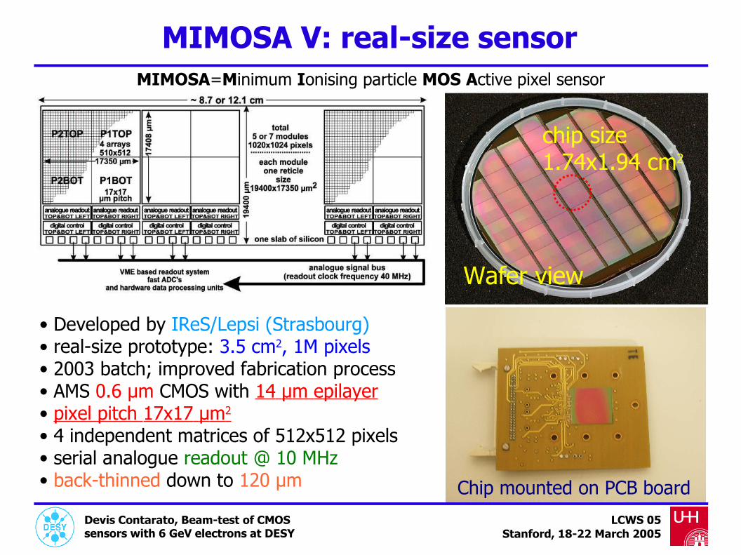
MIMOSA V: real-size sensor
Devis Contarato, Beam-test of CMOS sensors with 6 GeV electrons at DESY
LCWS 05Stanford, 18-22 March 2005
• Developed by IReS/Lepsi (Strasbourg)• real-size prototype: 3.5 cm2, 1M pixels• 2003 batch; improved fabrication process• AMS 0.6 µm CMOS with 14 µm epilayer• pixel pitch 17x17 µm 2• 4 independent matrices of 512x512 pixels• serial analogue readout @ 10 MHz• back-thinned down to 120 µm
chip size 1.74x1.94 cm2
Wafer view
Chip mounted on PCB board
MIMOSA=Minimum Ionising particle MOS Active pixel sensor
DESY activities on CMOS sensors
Devis Contarato, Beam-test of CMOS sensors with 6 GeV electrons at DESY
LCWS 05Stanford, 18-22 March 2005
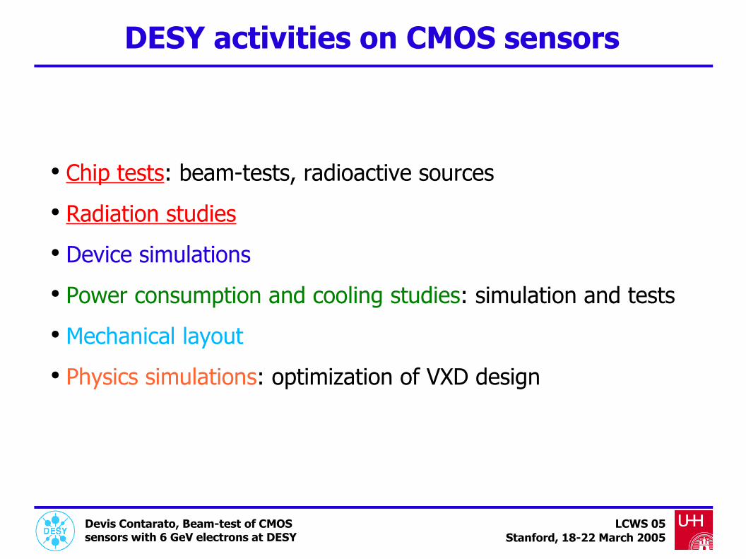
● Chip tests: beam-tests, radioactive sources● Radiation studies● Device simulations● Power consumption and cooling studies: simulation and tests● Mechanical layout● Physics simulations: optimization of VXD design

Beam-tests at DESY II
Devis Contarato, Beam-test of CMOS sensors with 6 GeV electrons at DESY
LCWS 05Stanford, 18-22 March 2005
● Electrons up to 6 GeV● 3 x-y planes silicon reference telescope● Event rate ~Hz (MAPS + reference telescope)● VME telescope readout + dedicated ADC board for MAPS● Cooling to –15°C● Dec '04 – Jan '05 run: 400000 events
3 x-y planes
Spill Counter
MAPS support + cooling box

The silicon reference telescope
Devis Contarato, Beam-test of CMOS sensors with 6 GeV electrons at DESY
LCWS 05Stanford, 18-22 March 2005
● Single-sided silicon microstrip detectors, 50 µm readout pitch● Detection efficiency >99%, S/N~45-85● Intrinsic resolution~3 µm, but in real life... multiple scattering!● In this work: track fitting with ~6 µm precision
S/N~55
e- @ 6 GeV

Experimental results: signal & S/N
Devis Contarato, Beam-test of CMOS sensors with 6 GeV electrons at DESY
LCWS 05Stanford, 18-22 March 2005
<S/N>~21
● 6 GeV electrons, cooling to -10°C● MPV for seed pixel signal ~340 e● ENC~20 electrons● Average Signal-to-Noise~21
MPV~340 e
ENC~20 e

Experimental results: cluster charge
Devis Contarato, Beam-test of CMOS sensors with 6 GeV electrons at DESY
LCWS 05Stanford, 18-22 March 2005
● Average cluster size ~6 (cut of S/N>2 for neighbors) ● Most of the charge collected within 9 pixel (then fluctuations)● Charge sharing is symmetric!
S/Nneigh
>2
MPV~946 e MPV~940 e

Signal-to-Noise: temperature dependence
Devis Contarato, Beam-test of CMOS sensors with 6 GeV electrons at DESY
LCWS 05Stanford, 18-22 March 2005
Average noise vs T<S/N> vs T
● Measurements performed from -15°C to +5°C ● Cooling is needed to keep noise level low w.r.t. room T
● Slight dependence of S/N between -15°C and +5°C
Leakage current term
)2
exp(210 Tk
ETccnoise
B
g−+=
(bars= RMS of pixel distribution)
Noise ∝ (Ileak)1/2

Irradiation with 10 MeV electrons
Devis Contarato, Beam-test of CMOS sensors with 6 GeV electrons at DESY
LCWS 05Stanford, 18-22 March 2005
● Performed at the S-DALINAC of Darmstadt Technical University (Germany)
● 9.4 MeV electrons (tunable), current~1 nA
● Irradiation under bias & clock
● 2 different fluences (~background in 1st VXD layer) on 2 different matrices
Readout electronics
Matrix T02Matrix T01
Matrix B02Matrix B01
3×10¹² e/cm2
(~70 krad)
1×10¹³ e/cm2
(~230 krad)
electron beam(spot~6x6 mm2)
Copper plate for beam-current measurement
Chip control signals
-10°C

Preliminary results from 55Fe calibration
Devis Contarato, Beam-test of CMOS sensors with 6 GeV electrons at DESY
LCWS 05Stanford, 18-22 March 2005
● Measurements performed at -10°C
● Pedestal levels strongly and non-uniformly shifted after irradiation (but correlated with dose)
● Loss in performance observed from calibration characteristics
● Further studies under way!
5.9 keV peak
?
PRELIMINARY!

Conclusions & Outlook
Devis Contarato, Beam-test of CMOS sensors with 6 GeV electrons at DESY
LCWS 05Stanford, 18-22 March 2005
Beam-test of CMOS sensors with 6 GeV electrons at DESY● Results for signal, S/N and noise consistent with known values (from Strasbourg tests)● No significant temperature effect observed between -15°C and +5°C ● Efficiency still under study
Irradiation with 10 MeV electrons● Irradiation at doses comparable with expectations for first VXD layer background● Preliminary results from 55Fe calibration show loss in performance after 3×10¹²
e/cm2: further investigations under way
Next steps● Efficiency check: priority!● Improve telescope performance/alignment: eventual position resolution studies from energy scans ● Beam-test of irradiated chip