Design of a RF CMOS Low Noise Amplifier
32
DESIGN OF RF CMOS LOW NOISE PRE-AMPLIFIER Nirav Desai
Transcript of Design of a RF CMOS Low Noise Amplifier
DESIGN OF RF CMOS LOW NOISE PRE-AMPLIFIER
Nirav Desai
2
Abstract:
This project examines the issues involved in the design of RF CMOS Pre – Amplifiers.
The effects of channel length modulation, body effect and gate – drain capacitance on the
design equations for power constrained simultaneous noise and input matching are
analyzed and presented. An algorithmic approach towards the design of CMOS LNAs
given a fixed center frequency and constraints on power dissipation is presented.
3
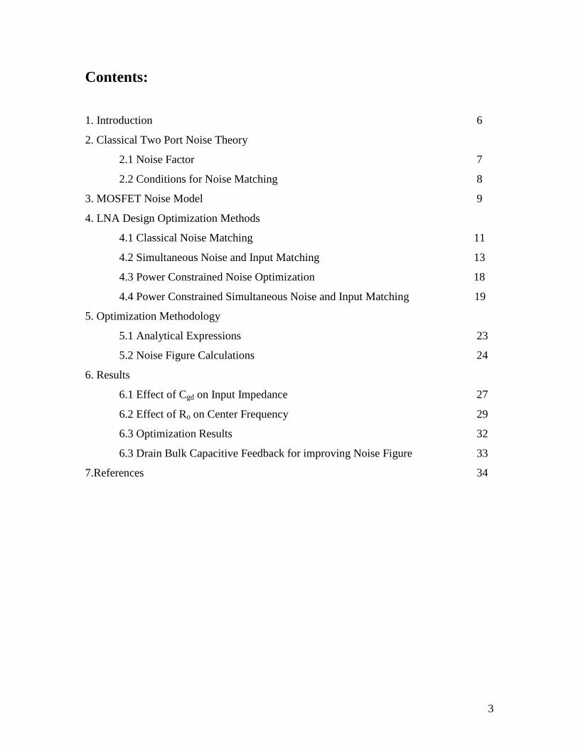
Contents:
1. Introduction 6
2. Classical Two Port Noise Theory
2.1 Noise Factor 7
2.2 Conditions for Noise Matching 8
3. MOSFET Noise Model 9
4. LNA Design Optimization Methods
4.1 Classical Noise Matching 11
4.2 Simultaneous Noise and Input Matching 13
4.3 Power Constrained Noise Optimization 18
4.4 Power Constrained Simultaneous Noise and Input Matching 19
5. Optimization Methodology
5.1 Analytical Expressions 23
5.2 Noise Figure Calculations 24
6. Results
6.1 Effect of Cgd on Input Impedance 27
6.2 Effect of Ro on Center Frequency 29
6.3 Optimization Results 32
6.3 Drain Bulk Capacitive Feedback for improving Noise Figure 33
7.References 34
4
1. Introduction:
RF designs are increasingly taking advantage of technological advances in CMOS that
make possible the integration of complete communications systems. The use of CMOS
technologies for implementation of the front end electronics in a wireless communication
system is therefore attractive because of the promise of integrating the whole system on a
single chip.
Received signal power levels at the antenna are around 130 dBm, and this low level
degrades further in the presence of physical obstructions such as buildings and trees.
Hence, a good low noise amplifier (LNA) at the front end is critical for enabling robust
performance in obstructed environments.
In the design of low noise amplifiers, there are several common goals. These include
minimizing the noise figure of the amplifier, providing gain with sufficient linearity and
providing a stable 50 input impedance to terminate an unknown length of transmission
line which delivers signal from the antenna to the amplifier. A good input match is even
more critical when a pre select filter precedes the LNA because such filters are often
sensitive to the quality of their terminating impedances. The additional constraint of low
power consumption which is imposed on portable systems further complicates the design
process.
This project studies the effects of channel length modulation, body effect and device
capacitance on the input matching and noise matching conditions required for power
constrained LNA design.
5
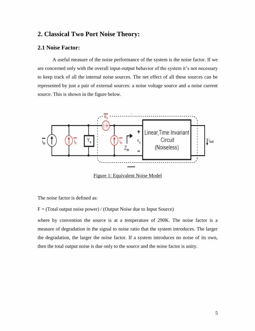
2. Classical Two Port Noise Theory:
2.1 Noise Factor:
A useful measure of the noise performance of the system is the noise factor. If we
are concerned only with the overall input-output behavior of the system it’s not necessary
to keep track of all the internal noise sources. The net effect of all these sources can be
represented by just a pair of external sources: a noise voltage source and a noise current
source. This is shown in the figure below.
Figure 1: Equivalent Noise Model
The noise factor is defined as:
F = (Total output noise power) / (Output Noise due to Input Source)
where by convention the source is at a temperature of 290K. The noise factor is a
measure of degradation in the signal to noise ratio that the system introduces. The larger
the degradation, the larger the noise factor. If a system introduces no noise of its own,
then the total output noise is due only to the source and the noise factor is unity.
6
2.2 Conditions for Noise Matching
If we assume that the noise powers of the source and the two port network are
uncorrelated, then
In order to accommodate the possibility of correlation between en and in we can express it
as a sum of two components: One, ic is correlated with en and other iu is not.
in = ic + iu
Since ic is correlated to en it may be treated as proportional to it through a constant whose
dimensions are those of an admittance.
ic= Yc * en
Yc is known as the correlation admittance.
Given these equations the noise factor for the system may be expressed as:
])()[( 22
min optsopts
s
n BBGGG
RFF
where 2
c
n
u
opt GR
GG and copt BB
where Yc = Gc + j*Bc and the noise parameters are defined as:
fkT
eR n
n
4
2
fkT
iG u
u
4
2
fkT
iG s
s
4
2
Hence to minimize the noise factor, the source susceptance should be equal to the inverse
of the correlation susceptance, while the source conductance should be set equal to Gopt.
Thus the contours of constant noise factor are non-overlapping circles in the admittance
plane.
2
22 ||
s
snns
i
YeiiF
7
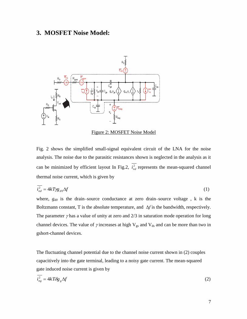
3. MOSFET Noise Model:
Figure 2: MOSFET Noise Model
Fig. 2 shows the simplified small-signal equivalent circuit of the LNA for the noise
analysis. The noise due to the parasitic resistances shown is neglected in the analysis as it
can be minimized by efficient layout In Fig.2, 2
ndi represents the mean-squared channel
thermal noise current, which is given by
fgkTi dnd 0
2 4 (1)
where, gd0 is the drain–source conductance at zero drain–source voltage , k is the
Boltzmann constant, T is the absolute temperature, and ∆f is the bandwidth, respectively.
The parameter has a value of unity at zero and 2/3 in saturation mode operation for long
channel devices. The value of increases at high Vgs and Vds and can be more than two in
gshort-channel devices.
The fluctuating channel potential due to the channel noise current shown in (2) couples
capacitively into the gate terminal, leading to a noisy gate current. The mean-squared
gate induced noise current is given by
fgkTi gng 42 (2)
8
where
0
22
5 d
gs
gg
Cg
(3)
is a constant with value of 4/3 in long-channel devices, and Cgs represents the gate–
source capacitance of the input transistor. Like , the value of also increases in short
channel devices and at high Vds and Vgs . Since the gate-induced noise current has a
correlation with the channel noise current, a correlation coefficient is defined as follows:
22
ndng
ndng
ii
iic
(4)
With long channel devices, c can be predicted theoretically as 0.395j. The value of c is
purely imaginary, reflecting the capacitive coupling between the channel and gate-
induced noise sources.
9
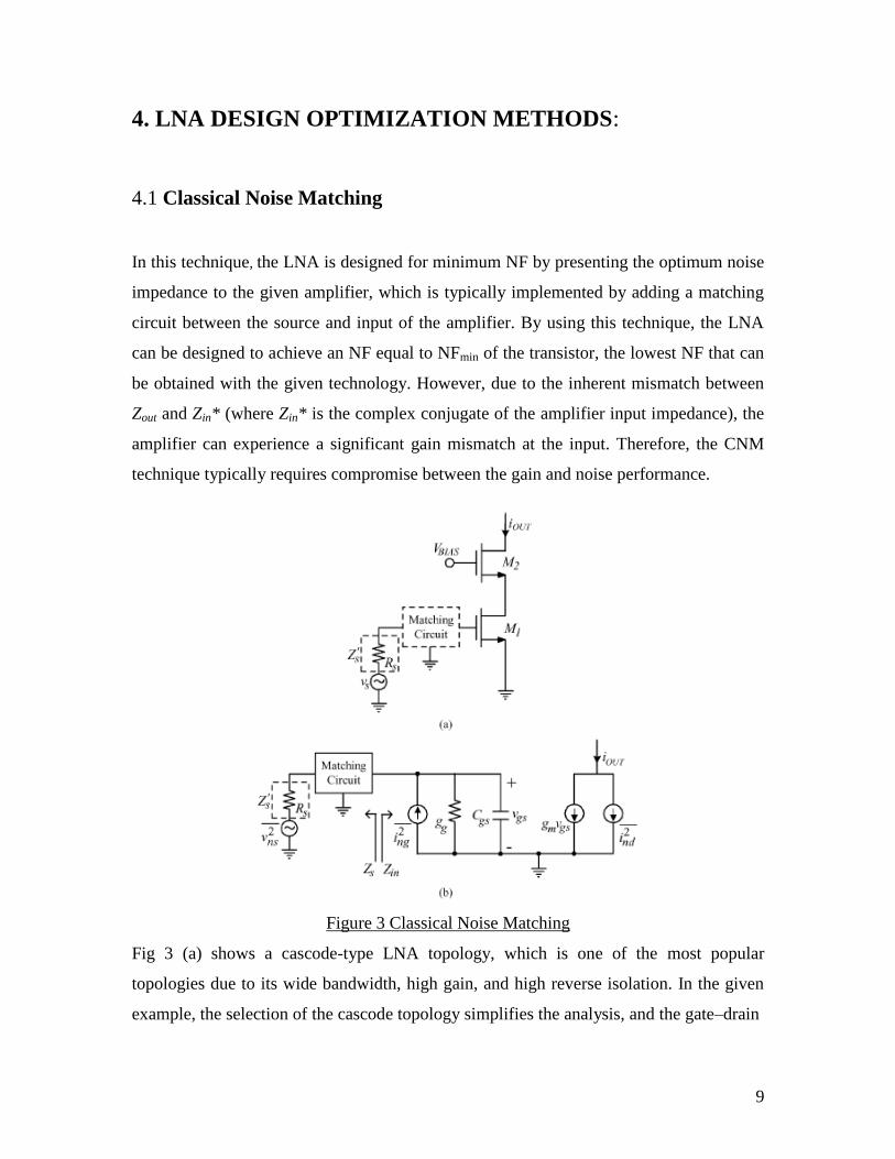
4. LNA DESIGN OPTIMIZATION METHODS:
4.1 Classical Noise Matching
In this technique, the LNA is designed for minimum NF by presenting the optimum noise
impedance to the given amplifier, which is typically implemented by adding a matching
circuit between the source and input of the amplifier. By using this technique, the LNA
can be designed to achieve an NF equal to NFmin of the transistor, the lowest NF that can
be obtained with the given technology. However, due to the inherent mismatch between
Zout and Zin* (where Zin* is the complex conjugate of the amplifier input impedance), the
amplifier can experience a significant gain mismatch at the input. Therefore, the CNM
technique typically requires compromise between the gain and noise performance.
Figure 3 Classical Noise Matching
Fig 3 (a) shows a cascode-type LNA topology, which is one of the most popular
topologies due to its wide bandwidth, high gain, and high reverse isolation. In the given
example, the selection of the cascode topology simplifies the analysis, and the gate–drain
10
capacitance can be neglected.
Fig. 3 (b) shows the simplified small-signal equivalent circuit of the cascode amplifier for
the noise analysis including the intrinsic transistor noise model. In Fig. 3 (b), the effects
of the common-gate transistor on the noise and frequency response are neglected , as well
as the parasitic resistances of gate, body, source, and drain terminal.
The noise parameters for the cascode amplifier shown in Fig. 3 (a) can be expressed as
m
ng
R10
(5)
5||1)||1(
5
20 csCcCY gsgsopt (6)
)||1(5
21 20
min cFT
(7)
where Rn0 represents the noise resistance,Y
0opt is the optimum noise admittance, and F
omin
is the minimum noise factor, respectively. The cutoff frequency T is equal togs
m
Cg
,
and 0d
m
gg
is unity for long-channel devices and decreases as channel length scales
down.
Note that, from Fig. 3 (b), the input admittance is purely capacitive i.e. Y0
in = jCgs. By
comparing the complex conjugate of Y0in with the expression for Y
0opt, it can be seen that
the optimum source admittance for input matching is inherently different from that of the
noise matching in both real and imaginary parts. Thus, with the given example, one
cannot obtain both input matching and minimum NF simultaneously. This is the main
11
limitation of the CNM technique when applied to the LNA topology shown in Fig. 3 (a).
Note that the imaginary component of Y0opt is inductive, but the frequency response is
like that of a capacitor. Hence, there is a fundamental limitation in achieving broad-band
noise matching.
12
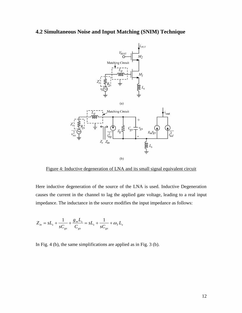
4.2 Simultaneous Noise and Input Matching (SNIM) Technique
Figure 4: Inductive degeneration of LNA and its small signal equivalent circuit
Here inductive degeneration of the source of the LNA is used. Inductive Degeneration
causes the current in the channel to lag the applied gate voltage, leading to a real input
impedance. The inductance in the source modifies the input impedance as follows:
sT
gs
s
gs
sm
gs
sin LsC
sLC
Lg
sCsLZ
11
In Fig. 4 (b), the same simplifications are applied as in Fig. 3 (b).
13
The noise factor and noise parameters for this circuit can be given by
)()()||1(5
5||1)(
5||1)(1
11 2222
2
2
2
2
02 gsgsm
sgs
sggs
d
sm
sLRsCgc
cRsC
cLLCs
gRg
F
(8)
m
nng
RR10
(9)
soptopt sLZZ 0 (10)
)||1(5
21 20
minmin cFFT
(11)
In (9) – (11), the noise parameters with superscripted zeros are those of the cascode
amplifier with no degeneration.
2
2
2
2
0
0
5||1
)||1(5
5||1
)||1(51
cc
C
cjc
YZ
gs
opt
opt (12)
Note that, from (9) – (11), only Zopt is shifted and there is no change in Fmin and Rn. Also,
note that (9) – (11) are valid for any arbitrary matching circuits, as well as the source
impedance in Fig. 4. In addition, as shown in Fig. 4 (b), the input impedance of the given
LNA can be expressed as:
sT
gs
s
gs
sm
gs
sin LsC
sLC
Lg
sCsLZ
11 (13)
14
As can be seen from (13), the source degeneration generates the real part at the input
impedance. This is important because there is no real part in Zin without degeneration,
while there is in Zopt . Therefore, if not excessive, Ls helps to reduce the discrepancy
between the real parts of Zopt and Zin of the LNA. Furthermore, from (13), the imaginary
part of Zin is changed by sLs, and this is followed by the same change in Zopt, as shown in
(10).
From (12), (10) can be re-expressed as
s
gs
optopt sLsC
mZZ 1
Re 0 (14)
where the constant m, for the typical device parameters of long channel MOSFETs, is
approximately equal to 0.6. With technology scaling, the ratio / stays nearly constant at
2, becomes lower than 1, and c is slightly higher than 0.4 (e.g. c = 0.5 with 0.25-um
technology), such that the constant m is expected to become closer to 1. Therefore, from
(13) and (14), it can be seen that the inductive source degeneration helps to bring the Zopt
point close to the optimum source impedance point Zin* while causing no degradation in
Fmin and Rn. This characteristic reveals the potential for the SNIM technique. For the
circuit shown in Fig. 4 (a), the condition that allows the SNIM is
*
inopt ZZ (15)
From (9) – (11), and (13), the conditions that satisfy (15) and the matching with the
source impedance are as follows:
]Re[]Re[ sopt ZZ (16)
]Im[]Im[ sopt ZZ (17)
]Im[]Im[ sin ZZ (18)
]Re[]Re[ sin ZZ (19)
15
As described above, based on (13) and (14), (17) and (18) are the same, especially in any
advanced technology. Therefore, (18) could be dropped considering the importance of the
noise performance. Some amount of mismatch in the input matching has a negligible
effect on the LNA performance, while the mismatch in Zopt directly affects the NF. Now
then, from (9) – (13), the design parameters that can satisfy (16), (17), and (19) are Vgs,
the transistor size (W or L), and Ls. Minimum gate length is assumed to maximize the
transistor cutoff frequency T. Therefore, for the given value of Zs, (16), (17), and (19)
can be solved since three effective equations are provided with three unknowns.
Qualitatively, the LNA design based on the SNIM technique can be explained as follows.
Following (10), (12), and (16), for an arbitrary signal source impedance, choose a
transistor size (W), which satisfies
]Re[]Re[ sopt ZZ .
For the given transistor size Cgs, choose the degeneration inductor size Ls that satisfies
(17),
]Im[]Im[ sopt ZZ
For the given values of Cgs and Ls, the value of Vgs can then be determined from (19).
]Re[]Re[ sin ZZ
Note that, as discussed above, for the given Ls, the imaginary value of the optimum noise
impedance would automatically be approximately equal to that of the input impedance
with an opposite sign. Now, from Fig. 4 (b), if
'
ss ZZ
then the SNIM is achieved to the signal source impedance. If not, the matching circuit
shown in Fig. 4 should be added. The design methodology described above guarantees
the NF of the LNA equal to of the common-source transistor with nearly perfect input
impedance matching.
16
The above LNA design technique suggests that, by the addition of Ls, in principle, the
SNIM can be achieved for any value of Zopt by satisfying (16), (17), and (19) assuming
(9) – (11) are valid. Many cases, especially those with large transistor size, high power
dissipation, and high frequency of operation [i.e., (16), (17), and (19)] can be satisfied
without much difficulty, while (9) – (11) stay valid. The problem occurs when the
transistor size is small (hence, the power dissipation is small) and the LNA operates at
low frequencies. Equation (12) indicates that the small transistor size and/or low
frequency leads to high value of Re[Zopt]. Therefore, from (13), for the given bias point
or T , the degeneration inductor has to be very large to satisfy (19). The problem is that
for the Ls to be greater than some value, (11) becomes invalid and increases significantly.
As a result, the minimum achievable NF of the LNA can be considerably higher than of
the common-source transistor, spoiling the idea of SNIM. In other words, the SNIM
technique is not applicable for the transistor sizes and bias levels (or the power
dissipation levels) as Re[Zopt] becomes greater than Re[Zin] for the value of Ls, which
does not degrade the of the LNA. The inaccuracy of (11) for large Ls, might be caused by
the negligence of Cgd. With large Ls, the transconductance of the common-source stage
can degrade significantly and the feedback signal through Cgd could become non
negligible. As a practical design technique, the minimum value of Ls, which does not
degrade Fmin, can be identified by monitoring the Fmin of the LNA as a function of Ls in
simulation.
Note that, from (13), even with a small transistor, low power, and low frequency, input
matching can still be satisfied by proper selection of the degeneration inductance. It was
found that, for the small amount of power dissipation where the SNIM technique is not
applicable, there exists an optimum transistor size that provides a minimum NF while
satisfying input matching. However, the achievable minimum NF is higher than of the
common-source transistor.
17
4.3 Power Constrained Noise Optimization
With a constrained amount of power dissipation, the simultaneous gain and noise
matching approach can still be useful. At any given amount of power dissipation, (18)
and (19) can be satisfied by the proper selection of Ls for the given Cgs with the help of
the matching circuit shown in Fig. 4, which is typically implemented by a series
inductance Lg. It can be shown that, under fixed drain current and while satisfying (18)
and (19), there exists a transistor size where the NF of the amplifier becomes minimum.
This optimum transistor size is given by
optinsox
optQRC
W,3
1
(20)
51
||
311
5||
2,c
cQ optin (21)
In (20), Cox represents the gate–oxide capacitance of the MOSFET per unit area. The
minimum NF in this case can be given by
T
PF
4.21min (22)
FminP is higher than Fmin, the minimum NF of the common-source transistor. The reason
for this is due to the mismatch between Zs and Zopt and/or the high values of Ls, which
leads to higher Fmin, as discussed previously.
18
4.4. Power Constrained Simultaneous Noise and Input Matching
(PCSNIM) Technique
SNIM and PCNO techniques do not allow SNIM at low-power implementations.
However, the need for low-power implementation of a radio transceiver is one of the
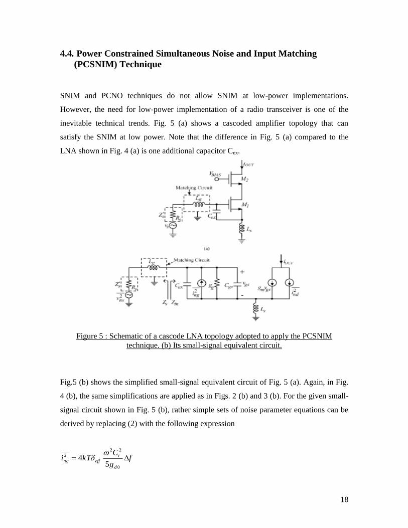
inevitable technical trends. Fig. 5 (a) shows a cascoded amplifier topology that can
satisfy the SNIM at low power. Note that the difference in Fig. 5 (a) compared to the
LNA shown in Fig. 4 (a) is one additional capacitor Cex.
Figure 5 : Schematic of a cascode LNA topology adopted to apply the PCSNIM
technique. (b) Its small-signal equivalent circuit.
Fig.5 (b) shows the simplified small-signal equivalent circuit of Fig. 5 (a). Again, in Fig.
4 (b), the same simplifications are applied as in Figs. 2 (b) and 3 (b). For the given small-
signal circuit shown in Fig. 5 (b), rather simple sets of noise parameter equations can be
derived by replacing (2) with the following expression
fg
CkTi
d
t
effng 0
22
2
54
19
where eff = 2
2
t
gs
C
C and Ct = Cgs + Cex . Equation (23) is the same expression as (2),
but is just rewritten for simpler mathematics. The noise parameters can be given by
m
ng
R1
(24)
2
2
2
2
5||
)||1(5
5||
)||1(5
cC
C
cC
cC
Cj
cZ
gs
t
gs
gs
t
opt (25)
)||1(5
21 2
min cFT
(26)
Interestingly, as can be seen from (24) and (26), the noise resistance and minimum NF
are not affected by the addition of Cex, which is the same as the cases shown in Figs. 2
and 3. From Fig. 5 (b), the input impedance of the LNA can be given by
gs
sm
gs
sinC
Lg
sCsLZ
1
It can now be seen that the (24) – (27) are similar to (9) – (11) and (13). Equations (24) –
(26) are valid for rather small values of Lg. As with the LNA topology shown in Fig.3 (a),
for the SNIM of the circuit shown in Fig. 4 (a), (15) now needs to be satisfied, and that
means that the conditions shown in (16) – (19) should be satisfied. From (25) and (27),
(16) – (19) can be re-expressed as
2
2
2
2
5||
)||1(5
)||1(5]Re[
cC
C
cC
cZ
gs
t
gs
s (28)
20
2
2
2
5||
)||1(5
5||
]Im[
cC
C
cC
cC
Cj
Z
gs
t
gs
gs
t
s (29)
t
sssC
sLZ1
]Im[ (30)
t
sm
sC
LgZ ]Re[ (31)
For the typical values of advanced CMOS technology parameters, (29) is approximately
equal to (30). Therefore, (30) can be dropped, which means that, for the given value of
Lg, the imaginary value of the optimum noise impedance becomes approximately equal to
that of the input impedance with an opposite sign automatically. The design parameters
that can satisfy (28), (29), and (31) are Vgs, W, Lg and Cex. Since there are three equations
and four unknowns, (28), (29), and (31) can be solved for an arbitrary value of Zs by
fixing the value of one of the design parameters. Therefore, in the PCSNIM LNA design
technique, by the addition of an extra capacitor, the SNIM can be achieved at any level of
power dissipation.
The qualitative description of the PCSNIM design process would be as follows:
First, choose the dc-bias Vgs, for example, the bias point that provides minimum Fmin.
Second, choose the transistor size W based on the power constraint. Third, choose the
additional capacitance Cex, as well as the degeneration inductance Lg to satisfy (28) and
(31) simultaneously. The value of Cex should be chosen considering the compromise
between the size of Lg and the available power gain. As described before, too much Lg
can lead to the increase in Fmin, while large Cex leads to the gain reduction due to the
degradation of the effective cutoff frequency of the composite transistor (transistor
including Cex ). Note that, as discussed above, for the given Lg, the imaginary value of the
optimum noise impedance would automatically equal that of the input impedance with an
21
opposite sign. At this point, the SNIM is achieved. As the last step, if there exists any
mismatch, an impedance matching circuit can be added.
Considering the relationship between the cutoff frequency and the total input
capacitance, the addition of Cex leads to power-gain degradation. For example, if Cex =
3Cgs, the cutoff frequency fT of the LNA is expected to be reduced by a factor of four.
This would lead to the reduction of the maximum oscillation frequency by the factor 2 ,
71%, due to the square-root functional dependence of fmax on fT. Therefore, it could be
considered that the power gain is a slowly varying function of Cex.
The limitation of the PCSIM technique is the high value of noise resistance. From (24),
the noise resistance Rn of the proposed topology is not affected by the addition of Cex, but
depends only on the value of gm. Therefore, the small transistor size and low-power
dissipation can lead to very high Rn. High Rn can be a serious limitation for the practical
high-yield LNA design.
22
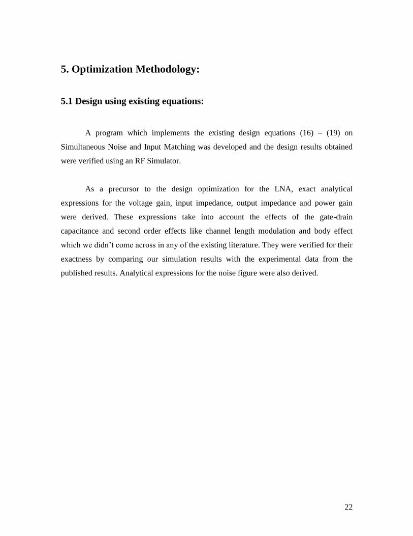
5. Optimization Methodology:
5.1 Design using existing equations:
A program which implements the existing design equations (16) – (19) on
Simultaneous Noise and Input Matching was developed and the design results obtained
were verified using an RF Simulator.
As a precursor to the design optimization for the LNA, exact analytical
expressions for the voltage gain, input impedance, output impedance and power gain
were derived. These expressions take into account the effects of the gate-drain
capacitance and second order effects like channel length modulation and body effect
which we didn’t come across in any of the existing literature. They were verified for their
exactness by comparing our simulation results with the experimental data from the
published results. Analytical expressions for the noise figure were also derived.
23
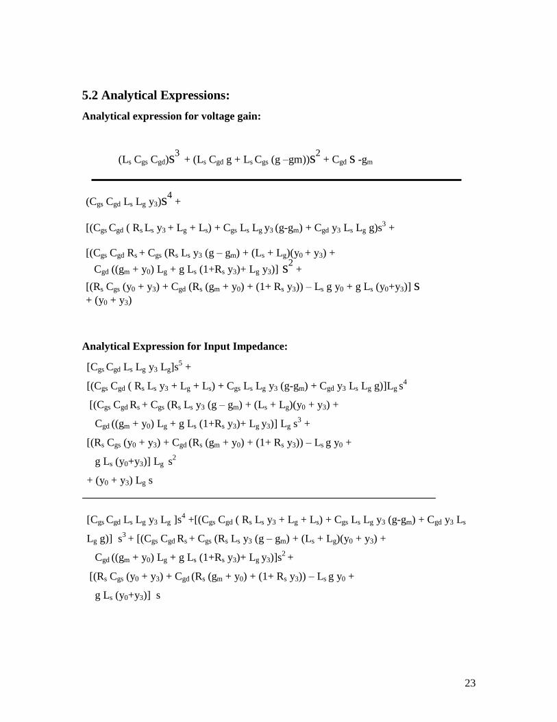
5.2 Analytical Expressions:
Analytical expression for voltage gain:
Analytical Expression for Input Impedance:
[Cgs Cgd Ls Lg y3 Lg]s5 +
[(Cgs Cgd ( Rs Ls y3 + Lg + Ls) + Cgs Ls Lg y3 (g-gm) + Cgd y3 Ls Lg g)]Lg s4
[(Cgs Cgd Rs + Cgs (Rs Ls y3 (g – gm) + (Ls + Lg)(y0 + y3) +
Cgd ((gm + y0) Lg + g Ls (1+Rs y3)+ Lg y3)] Lg s3 +
[(Rs Cgs (y0 + y3) + Cgd (Rs (gm + y0) + (1+ Rs y3)) – Ls g y0 +
g Ls (y0+y3)] Lg s2
+ (y0 + y3) Lg s
[Cgs Cgd Ls Lg y3 Lg ]s4 +[(Cgs Cgd ( Rs Ls y3 + Lg + Ls) + Cgs Ls Lg y3 (g-gm) + Cgd y3 Ls
Lg g)] s3
+ [(Cgs Cgd Rs + Cgs (Rs Ls y3 (g – gm) + (Ls + Lg)(y0 + y3) +
Cgd ((gm + y0) Lg + g Ls (1+Rs y3)+ Lg y3)]s2
+
[(Rs Cgs (y0 + y3) + Cgd (Rs (gm + y0) + (1+ Rs y3)) – Ls g y0 +
g Ls (y0+y3)] s
(Ls Cgs Cgd)s3
+ (Ls Cgd g + Ls Cgs (g –gm))s2 + Cgd s -gm
(Cgs Cgd Ls Lg y3)s4 +
[(Cgs Cgd ( Rs Ls y3 + Lg + Ls) + Cgs Ls Lg y3 (g-gm) + Cgd y3 Ls Lg g)s3 +
[(Cgs Cgd Rs + Cgs (Rs Ls y3 (g – gm) + (Ls + Lg)(y0 + y3) +
Cgd ((gm + y0) Lg + g Ls (1+Rs y3)+ Lg y3)] s2 +
[(Rs Cgs (y0 + y3) + Cgd (Rs (gm + y0) + (1+ Rs y3)) – Ls g y0 + g Ls (y0+y3)] s + (y0 + y3)
24
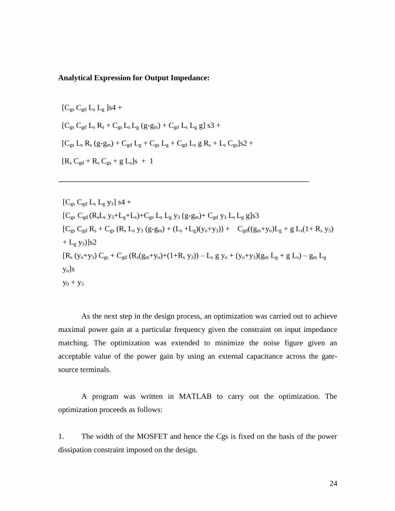
Analytical Expression for Output Impedance:
As the next step in the design process, an optimization was carried out to achieve
maximal power gain at a particular frequency given the constraint on input impedance
matching. The optimization was extended to minimize the noise figure given an
acceptable value of the power gain by using an external capacitance across the gate-
source terminals.
A program was written in MATLAB to carry out the optimization. The
optimization proceeds as follows:
1. The width of the MOSFET and hence the Cgs is fixed on the basis of the power
dissipation constraint imposed on the design.
[Cgs Cgd Ls Lg ]s4 +
[Cgs Cgd Ls Rs + Cgs Ls Lg (g-gm) + Cgd Ls Lg g] s3 +
[Cgs Ls Rs (g-gm) + Cgd Lg + Cgs Lg + Cgd Ls g Rs + Ls Cgs]s2 +
[Rs Cgd + Rs Cgs + g Ls]s + 1
[Cgs Cgd Ls Lg y3] s4 +
[Cgs Cgd (RsLs y3+Lg+Ls)+Cgs Ls Lg y3 (g-gm)+ Cgd y3 Ls Lg g]s3
[Cgs Cgd Rs + Cgs (Rs Ls y3 (g-gm) + (Ls +Lg)(yo+y3)) + Cgd((gm+yo)Lg + g Ls(1+ Rs y3)
+ Lg y3)]s2
[Rs (yo+y3) Cgs + Cgd (Rs(gm+yo)+(1+Rs y3)) – Ls g yo + (yo+y3)(gm Lg + g Ls) – gm Lg
yo]s
y0 + y3
25
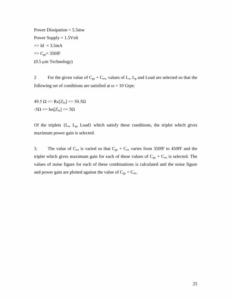
Power Dissipation < 5.5mw
Power Supply = 1.5Volt
=> Id = 3.5mA
=> Cgs= 350fF
(0.5 m Technology)
2 For the given value of Cgs + Cex, values of Ls, Lg and Load are selected so that the
following set of conditions are satisfied at = 10 Grps:
49.5 Ω <= Re[Zin] <= 50.5Ω
-5Ω <= Im[Zin] <= 5Ω
Of the triplets {Ls, Lg, Load} which satisfy these conditions, the triplet which gives
maximum power gain is selected.
3. The value of Cex is varied so that Cgs + Cex varies from 350fF to 450fF and the
triplet which gives maximum gain for each of these values of Cgs + Cex is selected. The
values of noise figure for each of these combinations is calculated and the noise figure
and power gain are plotted against the value of Cgs + Cex.
26
5.3 Noise Figure Calculations:
The equivalent noise voltage source 2
ne and the noise current source 2
ni represent the
noise generated by the system. 2
ne accounts for the effect of drain current noise and is
found by the reflecting the drain current noise to the input side. 2
ni is obtained by
reflecting the drain current noise source to the input side as an equivalent current source
combined with the induced gate current noise source already present on the input side of
the noise equivalent circuit for the LNA. This method is straightforward when the effect
of the gate drain capacitance is neglected, since this makes the circuit unilateral.
However, if the effect of the gate drain capacitance on the noise figure is to be included
the circuit loses its unilateral character, complicating the analysis.
Hence, we follow a method which is outlined below to facilitate the calculation of noise
figure of the system. Here, for calculating 2
ne , the drain current noise source is
represented as an equivalent noise resistance, whose value is decided according to the
equation
nd
d
nd
ndR
gfkT
iY
1
40
2
Now, the input impedance of the circuit is calculated by including Rnd in parallel with r0
in the circuit. Now 2
ne is calculated using,
2
ne = 2kT ∫ Re(Zin) df
where the integration is carried out in the band of interest.
27
Similarly, for the calculation of 2
ni , the drain current noise source is represented as an
equivalent noise resistance, and the induced gate current noise source is also represented
as a frequency dependent noise resistance by using the equation
ng
ng
ngRfkT
iY
1
4
2
Now, the input impedance of the circuit is calculated by including Rnd in parallel with r0
and Rng in parallel with Cgs in the circuit.
The value of the equivalent input noise current source is given by,
2
ni = 2kT ∫ Re(Yin1) df
Finally the noise figure for the system is calculated using the equation,
with Ys = 0.02 mho.
A design approach which tries to improve the noise performance by introducing
capacitive feedback between the drain and the bulk so as to increase the correlation
between the drain and the gate noise currents was considered. In this case also, exact
analytical expressions were derived for input impedance , voltage gain, output impedance
and power gain were derived taking into account the capacitances Cddbb and Csb.
Noise figure expressions were also found. The optimization procedure was carried out for
the new set of expressions.
2
22 ||
s
snns
i
YeiiF
28
6. RESULTS:
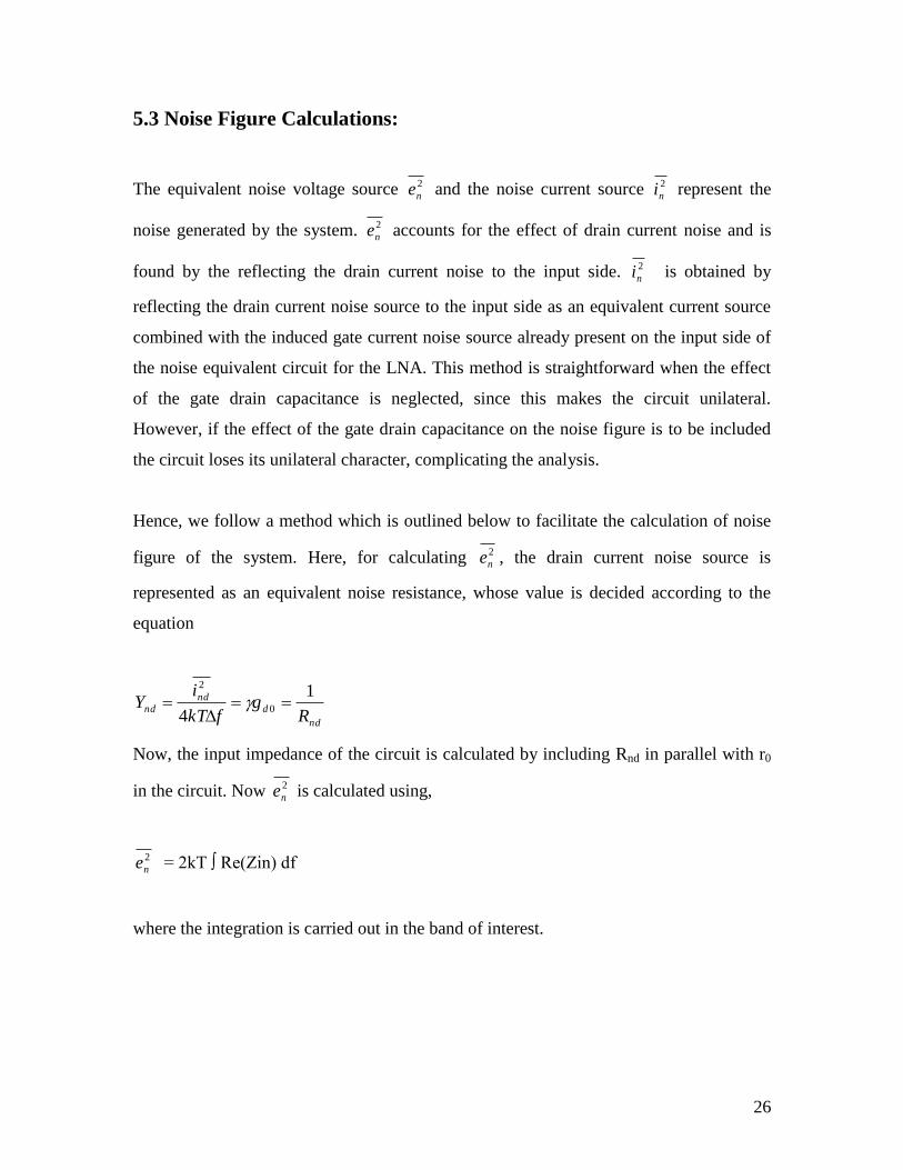
6.1 Effect of Cgd on Input Impedance:
Including the effect of Cgd reduces the resonant frequency of input loop and
reduces the input impedance as can be seen in these graphs:
Figure 6a: Input Impedance of the LNA (Cgd = 0)
Figure 6b: Input impedance of LNA (Cgd = 50fF)
29
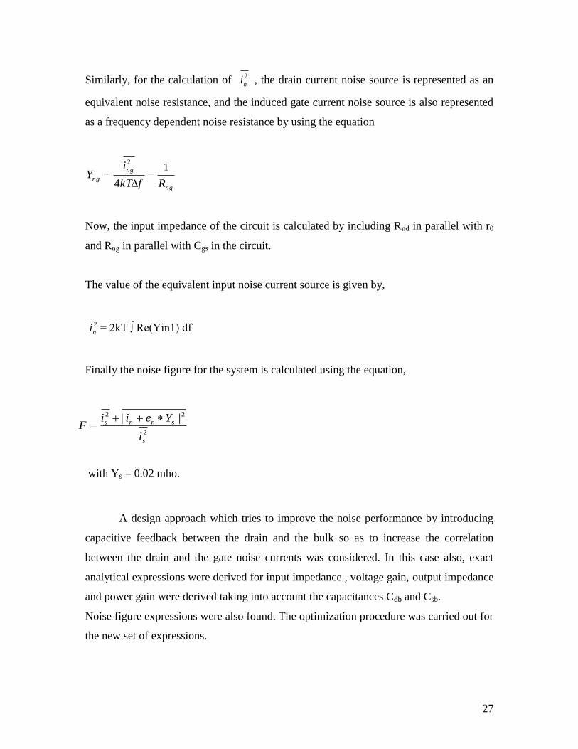
6.2 Effect of ro on center frequency:
Figure 7a: Input impedance of LNA with yo = 0.
Figure 7b: Input impedance of LNA with yo = (1/1500)
30
The finite output resistance alters the resistive term in the input impedance. The
resistive term becomes equal to T Ls only in the limit as ro becomes infinite. In general
the real part of Zin will be reduced and the imaginary pat may be altered as well shifting
the resonant frequency of the input loop. Depending on the relative resonant frequencies
of the input and output loops it is possible for a dip in the real part of the input impedance
to appear below at or above the desired center frequency of the overall amplifier.
However it is common for the dip to occur within a couple of percent of the center
frequency resulting in a poor input match somewhere in the band of interest.
31
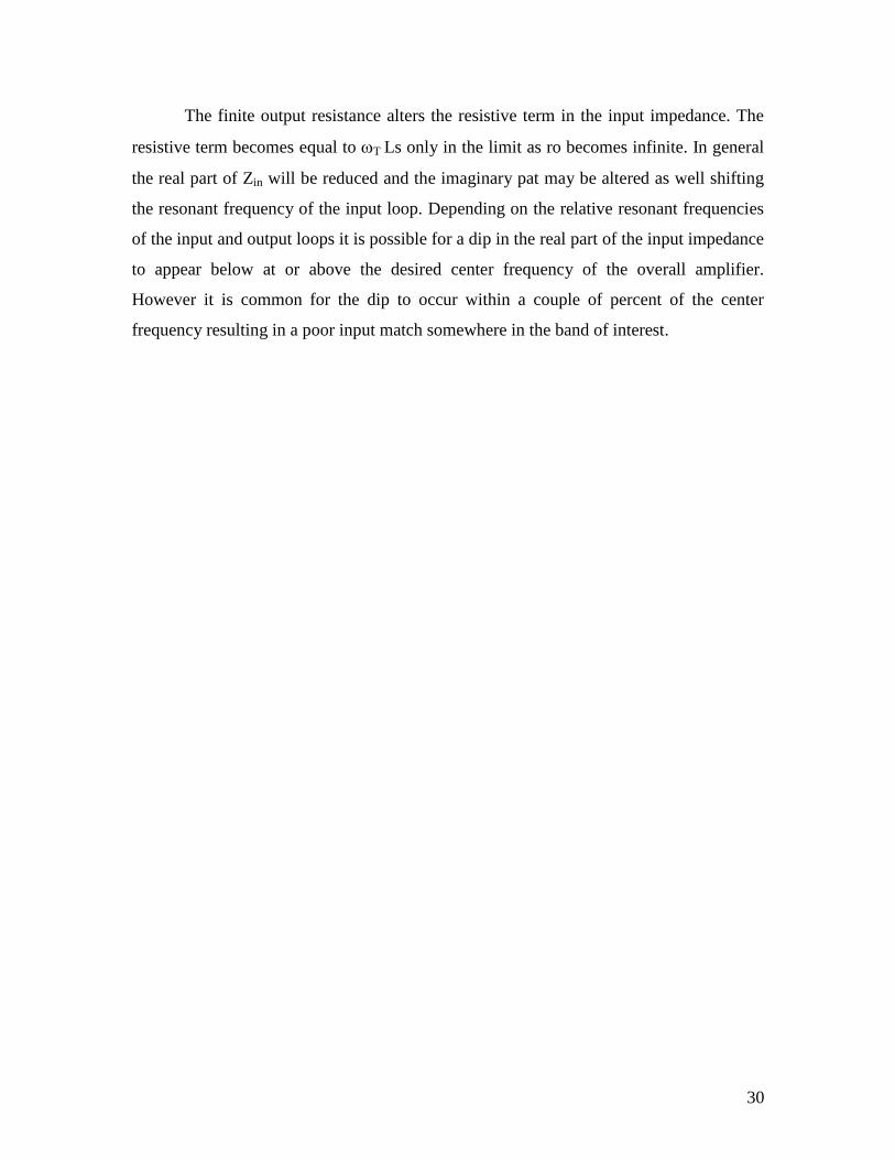
6.3 Optimization Results:
Legend:
X Axis: Ctotal = Cgs + Cex (fF)
Y axis: Power Gain (dB)
Noise Factor
It can be observed that a minimum noise figure of 1.95 is obtained at Ctotal =370fF and
the corresponding values of the components are:
Ls = 0.9nH
Lg = 18.2nH
Load = 70Ω
This gives a power gain of 9.88dB.
The noise figure is 0.5db less than the value at Ctotal = 350fF.
A lower noise figure of 1.9 was obtained for Ctotal = 430fF but the corresponding gain
being less than 9dB, this particular design was not considered.
32
7. References
1.)CMOS Low-Noise Amplifier Design Optimization Techniques
Trung-Kien Nguyen, Chung-Hwan Kim, Gook-Ju Ihm, Moon-Su Yang, and
Sang-Gug Lee
IEEE TRANSACTIONS ON MICROWAVE THEORY AND
TECHNIQUES, VOL. 52, NO. 5, MAY 2004
2.)Noise Modeling for RF CMOS Circuit Simulation
Andries J. Scholten, Luuk F. Tiemeijer, Ronald van Langevelde, Member, IEEE,
Ramon J. Havens, Adrie T. A. Zegers-van Duijnhoven, and Vincent C. Venezia
IEEE TRANSACTIONS ON ELECTRON DEVICES, VOL.50, NO. 3,
MARCH 2003
3.)MIT Open Course Ware
4.)RF CMOS Circuit Design
2nd Edition, Thomas H. Lee
5.) RF Microelectronics
Behzad Razavi
6.) A 1.5-V, 1.5-GHz CMOS Low Noise Amplifier
Derek K. Shaeffer, Student Member, IEEE, and Thomas H. Lee, Member, IEEE
IEEE JOURNAL OF SOLID-STATE CIRCUITS, VOL.32, NO. 5,
MAY 1997
7) Device Noise in Silicon RF Technologies
Samuel Martin, Vance D. Archer III, David M.Boulin,
Michel R. Frei, Kwok K. Ng, and Ran-Hong Yan
Bell Labs Technical Journal , Summer 1997