Td scdma (design)
56
TD-SCDMA DesignGuide August 2005
-
Upload
independent -
Category
Documents
-
view
4 -
download
0
Transcript of Td scdma (design)
TD-SCDMA DesignGuide
August 2005

Notice
The information contained in this document is subject to change without notice.
Agilent Technologies makes no warranty of any kind with regard to this material,including, but not limited to, the implied warranties of merchantability and fitnessfor a particular purpose. Agilent Technologies shall not be liable for errors containedherein or for incidental or consequential damages in connection with the furnishing,performance, or use of this material.
Warranty
A copy of the specific warranty terms that apply to this software product is availableupon request from your Agilent Technologies representative.
Restricted Rights Legend
Use, duplication or disclosure by the U. S. Government is subject to restrictions as setforth in subparagraph (c) (1) (ii) of the Rights in Technical Data and ComputerSoftware clause at DFARS 252.227-7013 for DoD agencies, and subparagraphs (c) (1)and (c) (2) of the Commercial Computer Software Restricted Rights clause at FAR52.227-19 for other agencies.
© Agilent Technologies, Inc. 1983-2005395 Page Mill Road, Palo Alto, CA 94304 U.S.A.
Acknowledgments
Mentor Graphics is a trademark of Mentor Graphics Corporation in the U.S. andother countries.
Microsoft®, Windows®, MS Windows®, Windows NT®, and MS-DOS® are U.S.registered trademarks of Microsoft Corporation.
Pentium® is a U.S. registered trademark of Intel Corporation.
PostScript® and Acrobat® are trademarks of Adobe Systems Incorporated.
UNIX® is a registered trademark of the Open Group.
Java™ is a U.S. trademark of Sun Microsystems, Inc.
SystemC® is a registered trademark of Open SystemC Initiative, Inc. in the UnitedStates and other countries and is used with permission.
ii

Contents1 TD-SCDMA Standard
Introduction............................................................................................................... 1-1Physical Layer .................................................................................................... 1-1
DesignGuide Examples Overview ............................................................................ 1-3
2 TD-SCDMA BER Performance DesignsIntroduction............................................................................................................... 2-112.2k Uplink Channel with AWGN............................................................................ 2-212.2k Uplink Fading Channel with Joint Detection Receiver .................................... 2-412.2k Downlink Fading Channel ............................................................................... 2-7
3 TD-SCDMA Instrument Link DesignsIntroduction............................................................................................................... 3-1Base Station Signal Generated Using ADS-ESGc Link Measured by VSA89600.... 3-2User Equipment Signal Generated Using ADS-ESGc Link Measured by VSA89600 3-5
4 TD-SCDMA Power Amplifier DesignsIntroduction............................................................................................................... 4-1Complementary Cumulative Distribution Function Measurements........................... 4-2Power vs. Time Measurement .................................................................................. 4-4CCDF and Spectrum Measurements of Multi-carrier Signal .................................... 4-6
5 TD-SCDMA Receiver DesignsIntroduction............................................................................................................... 5-1Base Station Reference Sensitivity Level ................................................................. 5-2User Equipment Adjacent Channel Selectivity ......................................................... 5-4
6 TD-SCDMA Signal Source DesignsIntroduction............................................................................................................... 6-1Uplink Signal Characteristics.................................................................................... 6-2Adjacent Channel Power Leakage Ratio .................................................................. 6-6Rate Match Calculator .............................................................................................. 6-8
7 TD-SCDMA Transmitter DesignsIntroduction............................................................................................................... 7-1Base Station Error Vector Magnitude ....................................................................... 7-2User Equipment Code Domain Power...................................................................... 7-5
Index
iii

iv
Chapter 1: TD-SCDMA Standard
IntroductionTD-SCDMA is a Chinese contribution to the international family of Mobile RadioSystems for 3G services of UMTS and IMT 2000. It is now one option of UTRA-TDD,called 1.28Mcps TDD or low chip rate (LCR) TDD. It is an advancedCDMA/TDMA/TDD system with an adaptive synchronous operation.
TD-SCDMA system simulation models based on the 3GPP TDD LCR standarddemonstrate signal generation capabilities; basic measurements are considered.TD-SCDMA aligns with the same version of the specification used by the AgilentESG-C, PSA II and VSA.
Physical Layer
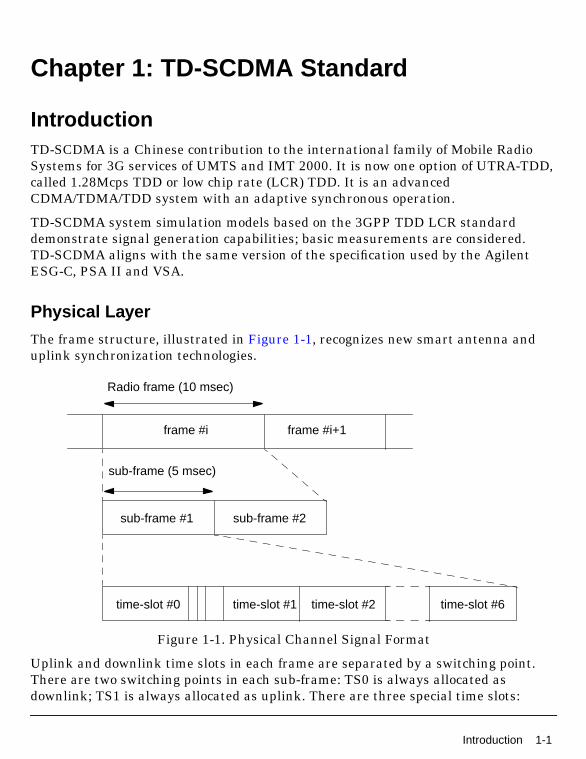
The frame structure, illustrated in Figure 1-1, recognizes new smart antenna anduplink synchronization technologies.
Figure 1-1. Physical Channel Signal Format
Uplink and downlink time slots in each frame are separated by a switching point.There are two switching points in each sub-frame: TS0 is always allocated asdownlink; TS1 is always allocated as uplink. There are three special time slots:
frame #i frame #i+1
Radio frame (10 msec)
sub-frame (5 msec)
sub-frame #1 sub-frame #2
time-slot #0 time-slot #1 time-slot #2 time-slot #6
Introduction 1-1
TD-SCDMA Standard
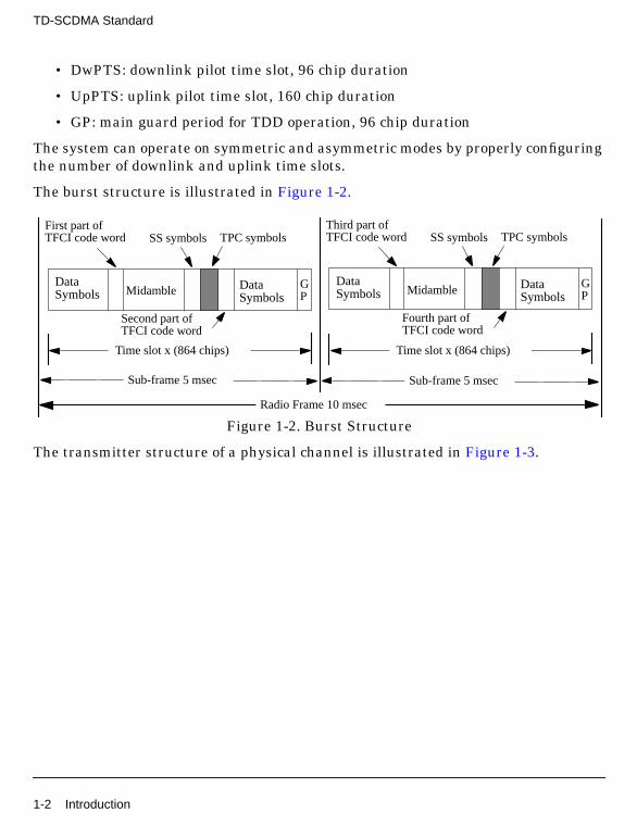
• DwPTS: downlink pilot time slot, 96 chip duration
• UpPTS: uplink pilot time slot, 160 chip duration
• GP: main guard period for TDD operation, 96 chip duration
The system can operate on symmetric and asymmetric modes by properly configuringthe number of downlink and uplink time slots.
The burst structure is illustrated in Figure 1-2.
Figure 1-2. Burst Structure
The transmitter structure of a physical channel is illustrated in Figure 1-3.
DataSymbols Midamble Data
SymbolsGP
First part ofSS symbolsTFCI code word TPC symbols
Second part ofTFCI code word
Time slot x (864 chips)
Sub-frame 5 msec
DataSymbols Midamble Data
SymbolsGP
Third part ofSS symbolsTFCI code word TPC symbols
Fourth part ofTFCI code word
Time slot x (864 chips)
Sub-frame 5 msec
Radio Frame 10 msec
1-2 Introduction

Figure 1-3. Physical Channel Transmitter Structure
There are two kinds of receiver algorithm for TD-SCDMA: Rake and Joint Detection.
Physical channels have a 3-layer structure.
• Time slot: 675 usec slot consisting of a number of Symbols. Time slots are usedin a TDMA component to separate different user signals in time and codedomain.
• Radio frame: 5 msec frame consisting of 7 time slots
• System frame numbering
DesignGuide Examples OverviewExample designs are provided in the /examples/tdscdma directory. Projects and theircorresponding design examples are:
The TDSCDMA_BER project demonstrates BER and BLER performance.
• BER and BLER performance of a 12.2k uplink channel with AWGN:TDSCDMA_12_2_UL_AWGN.dsn
• BER and BLER performance of a 12.2k uplink reference fading channel withjoint detection receiver: TDSCDMA_12_2_UL_Fading_JD.dsn
DesignGuide Examples Overview 1-3
TD-SCDMA Standard
• BER and BLER performance of a 12.2k downlink fading channel with jointdetection receiver: TDSCDMA_12_2_DL_Fading_JD.dsn
The TD-SCDMA_LinkTest project demonstrates the characteristics of ADS andinstrument links.
• Base station signal generated using ADS-ESGc link measured by VSA89600:TDSCDMA_DL_Link.dsn.
• User equipment signal generated using ADS-ESGc link measured byVSA89600: TDSCDMA_UL_Link.dsn.
The TDSCDMA_PA_Test project includes these design examples.
• Characterization of peak average power ratio versus probability:TDSCDMA_DL_CCDF.dsn.
• Instant and average power versus time measurements:TDSCDMA_UL_Power_vs_Time.dsn.
• CCDF and spectrum of multi-carrier signal measurements:TDSCDMA_MC_Test.dsn.
The TDSCDMA_Rx project demonstrates user equipment and base stationcharacteristics.
• BTS reference sensitivity level: TDSCDMA_UL_Sensitivity.dsn.
• UE adjacent channel selectivity: TDSCDMA_DL_AdjacentChannel.dsn.
The TDSCDMA_SignalSource project demonstrates the special transientcharacteristics of TD-SCDMA signals from time and frequency domains.
• Uplink signal characteristics: TDSCDMA_UL_Spectrum.dsn.
• Downlink signal characteristics: TDSCDMA_DL_ACLR.dsn.
The TDSCDMA_Tx project demonstrates user equipment and base stationcharacteristics.
• Base station error vector magnitude: TDSCDMA_DL_EVM.dsn.
• User equipment code domain power: TDSCDMA_UL_CDP.dsn.
1-4 DesignGuide Examples Overview

Chapter 2: TD-SCDMA BER PerformanceDesigns
IntroductionThe TDSCDMA_BER project demonstrates BER and BLER performance. Threeexample designs are included in this project:
• BER and BLER performance of a 12.2k uplink channel with AWGN:TDSCDMA_12_2_UL_AWGN.dsn
• BER and BLER performance of a 12.2k uplink reference fading channel withjoint detection receiver: TDSCDMA_12_2_UL_Fading_JD.dsn
• BER and BLER performance of a 12.2k downlink fading channel with jointdetection receiver: TDSCDMA_12_2_DL_Fading_JD.dsn
Introduction 2-1
TD-SCDMA BER Performance Designs
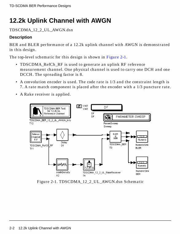
12.2k Uplink Channel with AWGNTDSCDMA_12_2_UL_AWGN.dsn
Description
BER and BLER performance of a 12.2k uplink channel with AWGN is demonstratedin this design.
The top-level schematic for this design is shown in Figure 2-1.
• TDSCDMA_RefCh_RF is used to generate an uplink RF referencemeasurement channel. One physical channel is used to carry one DCH and oneDCCH. The spreading factor is 8.
• A convolution encoder is used. The code rate is 1/3 and the constraint length is7. A rate match component is placed after the encoder with a 1/3 puncture rate.
• A Rake receiver is applied.
Figure 2-1. TDSCDMA_12_2_UL_AWGN.dsn Schematic
2-2 12.2k Uplink Channel with AWGN

Simulation Results
Simulation results are displayed in Figure 2-2.
Figure 2-2. Simulation Results
Benchmark
• Hardware Platform: Pentium 4 1.8GHz, 512 MB memory
• Software Platform: Windows XP, ADS 2003A
• Simulation Time: 20 hours
References
[1]3GPP Technical Specification TS 25.142 V4.5.0 “3rd Generation PartnershipProject; Technical Specification Group Radio Access Networks; Base stationConformance (TDD) (Release 4)” June, 2002.
12.2k Uplink Channel with AWGN 2-3
TD-SCDMA BER Performance Designs
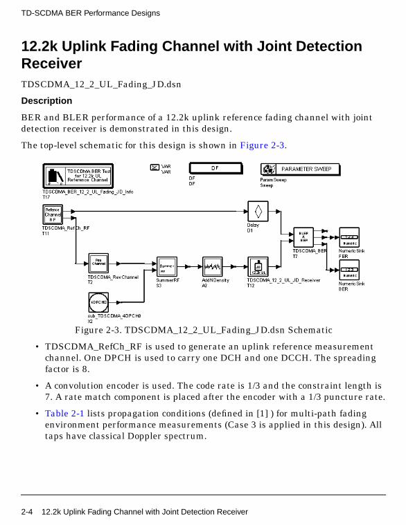
12.2k Uplink Fading Channel with Joint DetectionReceiverTDSCDMA_12_2_UL_Fading_JD.dsn
Description
BER and BLER performance of a 12.2k uplink reference fading channel with jointdetection receiver is demonstrated in this design.
The top-level schematic for this design is shown in Figure 2-3.
Figure 2-3. TDSCDMA_12_2_UL_Fading_JD.dsn Schematic
• TDSCDMA_RefCh_RF is used to generate an uplink reference measurementchannel. One DPCH is used to carry one DCH and one DCCH. The spreadingfactor is 8.
• A convolution encoder is used. The code rate is 1/3 and the constraint length is7. A rate match component is placed after the encoder with a 1/3 puncture rate.
• Table 2-1 lists propagation conditions (defined in [1] ) for multi-path fadingenvironment performance measurements (Case 3 is applied in this design). Alltaps have classical Doppler spectrum.
2-4 12.2k Uplink Fading Channel with Joint Detection Receiver
Simulation Results
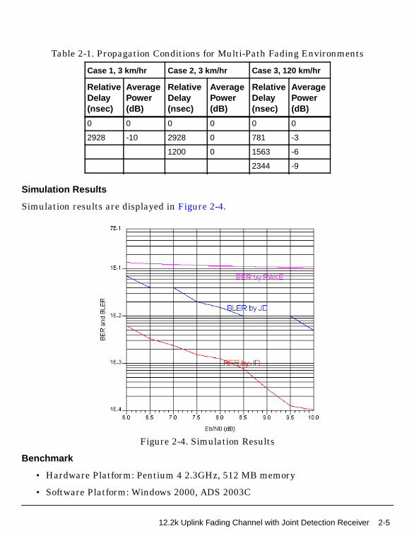
Simulation results are displayed in Figure 2-4.
Figure 2-4. Simulation Results
Benchmark
• Hardware Platform: Pentium 4 2.3GHz, 512 MB memory
• Software Platform: Windows 2000, ADS 2003C
Table 2-1. Propagation Conditions for Multi-Path Fading Environments
Case 1, 3 km/hr Case 2, 3 km/hr Case 3, 120 km/hr
RelativeDelay(nsec)
AveragePower(dB)
RelativeDelay(nsec)
AveragePower(dB)
RelativeDelay(nsec)
AveragePower(dB)
0 0 0 0 0 0
2928 -10 2928 0 781 -3
1200 0 1563 -6
2344 -9
12.2k Uplink Fading Channel with Joint Detection Receiver 2-5

TD-SCDMA BER Performance Designs
• Simulation Time: 60 hours
References
[1]3GPP Technical Specification TS 25.142 V4.5.0 “3rd Generation PartnershipProject; Technical Specification Group Radio Access Networks; Base stationConformance (TDD) (Release 4)” June, 2002.
2-6 12.2k Uplink Fading Channel with Joint Detection Receiver
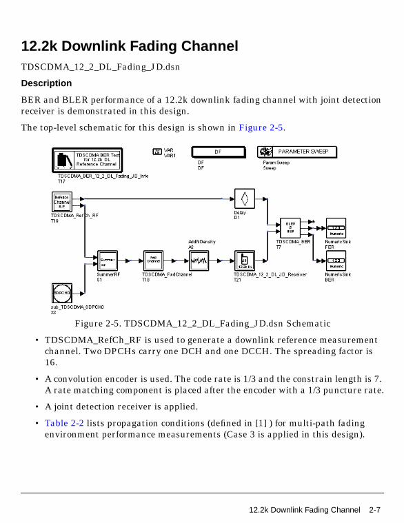
12.2k Downlink Fading ChannelTDSCDMA_12_2_DL_Fading_JD.dsn
Description
BER and BLER performance of a 12.2k downlink fading channel with joint detectionreceiver is demonstrated in this design.
The top-level schematic for this design is shown in Figure 2-5.
Figure 2-5. TDSCDMA_12_2_DL_Fading_JD.dsn Schematic
• TDSCDMA_RefCh_RF is used to generate a downlink reference measurementchannel. Two DPCHs carry one DCH and one DCCH. The spreading factor is16.
• A convolution encoder is used. The code rate is 1/3 and the constrain length is 7.A rate matching component is placed after the encoder with a 1/3 puncture rate.
• A joint detection receiver is applied.
• Table 2-2 lists propagation conditions (defined in [1] ) for multi-path fadingenvironment performance measurements (Case 3 is applied in this design).
12.2k Downlink Fading Channel 2-7
TD-SCDMA BER Performance Designs
Simulation Results
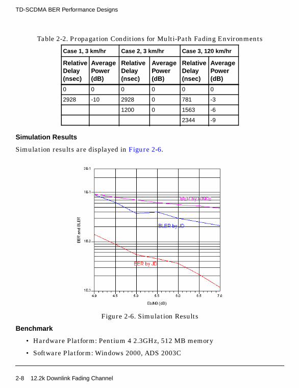
Simulation results are displayed in Figure 2-6.
Figure 2-6. Simulation Results
Benchmark
• Hardware Platform: Pentium 4 2.3GHz, 512 MB memory
• Software Platform: Windows 2000, ADS 2003C
Table 2-2. Propagation Conditions for Multi-Path Fading Environments
Case 1, 3 km/hr Case 2, 3 km/hr Case 3, 120 km/hr
RelativeDelay(nsec)
AveragePower(dB)
RelativeDelay(nsec)
AveragePower(dB)
RelativeDelay(nsec)
AveragePower(dB)
0 0 0 0 0 0
2928 -10 2928 0 781 -3
1200 0 1563 -6
2344 -9
2-8 12.2k Downlink Fading Channel

• Simulation Time: 35 hours
References
[1]3GPP Technical Specification TS 34.122 V4.5.0 “3rd Generation PartnershipProject; Technical Specification Group Radio Access Networks; Base stationConformance (TDD) (Release 4)” June, 2002.
12.2k Downlink Fading Channel 2-9
TD-SCDMA BER Performance Designs
2-10 12.2k Downlink Fading Channel
Chapter 3: TD-SCDMA Instrument LinkDesigns
IntroductionThe TD-SCDMA_LinkTest project demonstrates the characteristics of ADS andinstrument links. Design examples in this project are described in the followingsections:
• Base station signal generated using ADS-ESGc link measured by VSA89600:TDSCDMA_DL_Link.dsn.
• User equipment signal generated using ADS-ESGc link measured byVSA89600: TDSCDMA_UL_Link.dsn.
Introduction 3-1

TD-SCDMA Instrument Link Designs
Base Station Signal Generated Using ADS-ESGcLink Measured by VSA89600TDSCDMA_DL_Link.dsn
Description
This design demonstrates ADS and instrument links. The BTS signal is generatedusing ADS-ESGc link, then measured by VSA89600.
The top-level schematic for this design is shown in Figure 3-1.
• TDSCDMA_DL_RF is used to generate downlink RF signal.
• VSA_89600_1_Sink is used to start VSA89600 software to measure the RFsignal.
• ESG_E4438C_Sink is used to send I, Q data to ESG.
Figure 3-1. TDSCDMA_DL_Link.dsn Schematic
3-2 Base Station Signal Generated Using ADS-ESGc Link Measured by VSA89600
Simulation Results
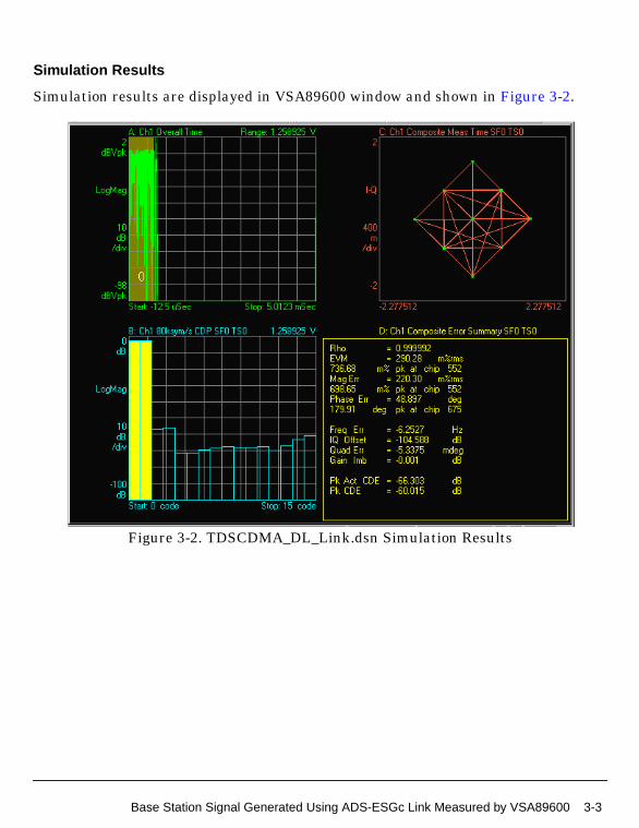
Simulation results are displayed in VSA89600 window and shown in Figure 3-2.
Figure 3-2. TDSCDMA_DL_Link.dsn Simulation Results
Base Station Signal Generated Using ADS-ESGc Link Measured by VSA89600 3-3

TD-SCDMA Instrument Link Designs
Benchmark
• Hardware Platform: Pentium III 800 MHz, 512 MB memory
• Software Platform: Windows 2000, ADS 2002C, VSA89600 4.00x2_BETA
• Simulation Time: N/A
References
[1]3GPP Technical Specification TS 25.142 V4.5.0 “3rd Generation PartnershipProject; Technical Specification Group Radio Access Networks; Base stationConfromance(TDD) (Release 4)” June, 2002.
3-4 Base Station Signal Generated Using ADS-ESGc Link Measured by VSA89600

User Equipment Signal Generated Using ADS-ESGcLink Measured by VSA89600TDSCDMA_UL_Link.dsn
Description
This design demonstrates ADS and instrument links. The user equipment signal isgenerated using ADS-ESGc link, then measured by VSA89600.
The top-level schematic for this design is shown in Figure 3-3.
• TDSCDMA_DL_RF is used to generate uplink RF signal.
• VSA_89600_1_Sink is used to start VSA89600 software to measure the RFsignal.
• ESG_E4438C_Sink is used to send I, Q data to ESG.
Figure 3-3. TDSCDMA_UL_Link.dsn Schematic
User Equipment Signal Generated Using ADS-ESGc Link Measured by VSA89600 3-5

TD-SCDMA Instrument Link Designs
Simulation Results
Simulation results are displayed in VSA89600 window and shown in Figure 3-4.
Figure 3-4. TDSCDMA_UL_Link.dsn Simulation Results
Benchmark
• Hardware Platform: Pentium III 800 MHz, 512 MB memory
• Software Platform: Windows 2000, ADS 2002C, VSA89600 4.00x2_BETA
• Simulation Time: N/A
References
[1]3GPP Technical Specification TS 25.142 V4.5.0 “3rd Generation PartnershipProject; Technical Specification Group Radio Access Networks; Base stationConfromance (TDD) (Release 4)” June, 2002.
3-6 User Equipment Signal Generated Using ADS-ESGc Link Measured by VSA89600

Chapter 4: TD-SCDMA Power AmplifierDesigns
IntroductionThe TDSCDMA_PA_Test project includes these design examples.
• Characterization of peak average power ratio versus probability:TDSCDMA_DL_CCDF.dsn.
• Instant and average power versus time measurements:TDSCDMA_UL_Power_vs_Time.dsn.
• CCDF and spectrum of multi-carrier signal measurements:TDSCDMA_MC_Test.dsn.
Introduction 4-1
TD-SCDMA Power Amplifier Designs
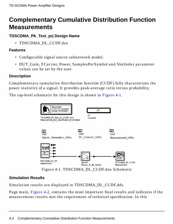
Complementary Cumulative Distribution FunctionMeasurementsTDSCDMA_PA_Test_prj Design Name
• TDSCDMA_DL_CCDF.dsn
Features
• Configurable signal source subnetwork model.
• DUT_Gain, FCarrier, Power, SamplesPerSymbol and SlotIndex parametervalues can be set by the user.
Description
Complementary cumulative distribution function (CCDF) fully characterizes thepower statistics of a signal. It provides peak-average ratio versus probability.
The top-level schematic for this design is shown in Figure 4-1.
Figure 4-1. TDSCDMA_DL_CCDF.dsn Schematic
Simulation Results
Simulation results are displayed in TDSCDMA_DL_CCDF.dds.
Page main, Figure 4-2, contains the most important final results and indicates if themeasurement results met the requirement of technical specification. In this
4-2 Complementary Cumulative Distribution Function Measurements
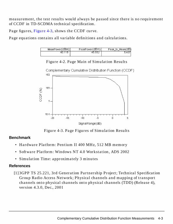
measurement, the test results would always be passed since there is no requirementof CCDF in TD-SCDMA technical specification.
Page figures, Figure 4-3, shows the CCDF curve.
Page equations contains all variable definitions and calculations.
Figure 4-2. Page Main of Simulation Results
Figure 4-3. Page Figures of Simulation Results
Benchmark
• Hardware Platform: Pentium II 400 MHz, 512 MB memory
• Software Platform: Windows NT 4.0 Workstation, ADS 2002
• Simulation Time: approximately 3 minutes
References
[1]3GPP TS 25.221, 3rd Generation Partnership Project; Technical SpecificationGroup Radio Access Network; Physical channels and mapping of transportchannels onto physical channels onto physical channels (TDD) (Release 4),version 4.3.0, Dec., 2001
Complementary Cumulative Distribution Function Measurements 4-3

TD-SCDMA Power Amplifier Designs
Power vs. Time MeasurementTDSCDMA_UL_Power_vs_Time.dsn
Features
• Power vs. time measurement
• 12.2kbps uplink reference measurement channel
• Roll-off root raised-cosine filter
Description
This example measures power vs. time for TD-SCDMA uplink. Power vs. time iscalculated by averaging the power of chips at the same position in all measuredsubframes.
The schematic for this design is shown in Figure 4-4. TDSCDMA_UL_RF generatesthe 12.2k measurement channel. TDSCDMA_PwrMeasure implements the powermeasurement.
Figure 4-4. TDSCDMA_Power_vs_Time Schematic
α 0.22=
4-4 Power vs. Time Measurement

Simulation Results
Simulation results are displayed in Figure 4-5.
The Equations page shows the equations that are used for calculating the mask.
Figure 4-5. Power vs. time for TD-SCDMA Uplink
Benchmark
• Hardware Platform: Pentium II 400 MHz, 512 MB memory
• Software Platform: Windows NT Workstation 4.0, ADS 2001
• Simulation Time: approximately 2 minutes
References
[1]3GPP TS 25.102, 3rd Generation Partnership Project; Technical SpecificationGroup Radio Access Network; UTRA(UE) TDD; Radio transmission andReception (Release 4), version 4.3.0, Dec., 2001
Power vs. Time Measurement 4-5
TD-SCDMA Power Amplifier Designs
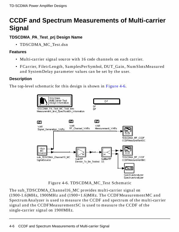
CCDF and Spectrum Measurements of Multi-carrierSignalTDSCDMA_PA_Test_prj Design Name
• TDSCDMA_MC_Test.dsn
Features
• Multi-carrier signal source with 16 code channels on each carrier.
• FCarrier, FiletrLength, SamplesPerSymbol, DUT_Gain, NumSlotsMeasuredand SystemDelay parameter values can be set by the user.
Description
The top-level schematic for this design is shown in Figure 4-6.
Figure 4-6. TDSCDMA_MC_Test Schematic
The sub_TDSCDMA_Channel16_MC provides multi-carrier signal on(1900-1.6)MHz, 1900MHz and (1900+1.6)MHz. The CCDFMeasurementMC andSpectrumAnalyzer is used to measure the CCDF and spectrum of the multi-carriersignal and the CCDFMeasurementSC is used to measure the CCDF of thesingle-carrier signal on 1900MHz.
4-6 CCDF and Spectrum Measurements of Multi-carrier Signal
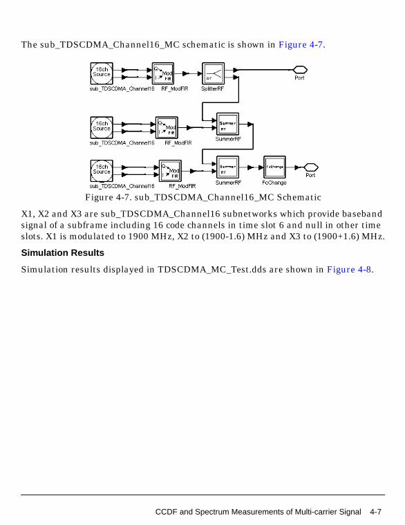
The sub_TDSCDMA_Channel16_MC schematic is shown in Figure 4-7.
Figure 4-7. sub_TDSCDMA_Channel16_MC Schematic
X1, X2 and X3 are sub_TDSCDMA_Channel16 subnetworks which provide basebandsignal of a subframe including 16 code channels in time slot 6 and null in other timeslots. X1 is modulated to 1900 MHz, X2 to (1900-1.6) MHz and X3 to (1900+1.6) MHz.
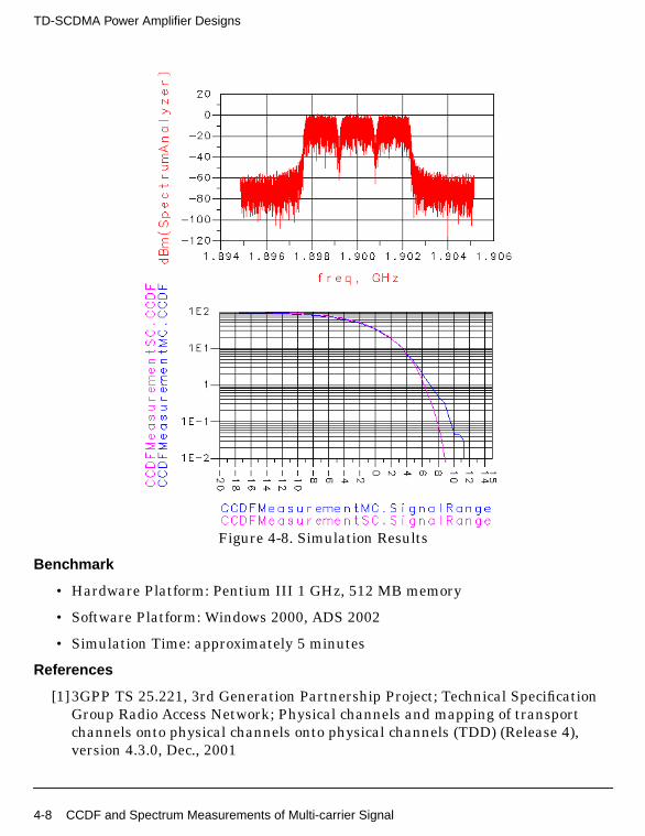
Simulation Results
Simulation results displayed in TDSCDMA_MC_Test.dds are shown in Figure 4-8.
CCDF and Spectrum Measurements of Multi-carrier Signal 4-7
TD-SCDMA Power Amplifier Designs
Figure 4-8. Simulation Results
Benchmark
• Hardware Platform: Pentium III 1 GHz, 512 MB memory
• Software Platform: Windows 2000, ADS 2002
• Simulation Time: approximately 5 minutes
References
[1]3GPP TS 25.221, 3rd Generation Partnership Project; Technical SpecificationGroup Radio Access Network; Physical channels and mapping of transportchannels onto physical channels onto physical channels (TDD) (Release 4),version 4.3.0, Dec., 2001
4-8 CCDF and Spectrum Measurements of Multi-carrier Signal
Chapter 5: TD-SCDMA Receiver Designs
IntroductionThe TD-SCDMA receiver project demonstrates user equipment and base stationcharacteristics. Design examples in this project are described in the followingsections:
• BTS reference sensitivity level: TDSCDMA_UL_Sensitivity.dsn.
• UE adjacent channel selectivity: TDSCDMA_DL_AdjacentChannel.dsn.
Introduction 5-1
TD-SCDMA Receiver Designs
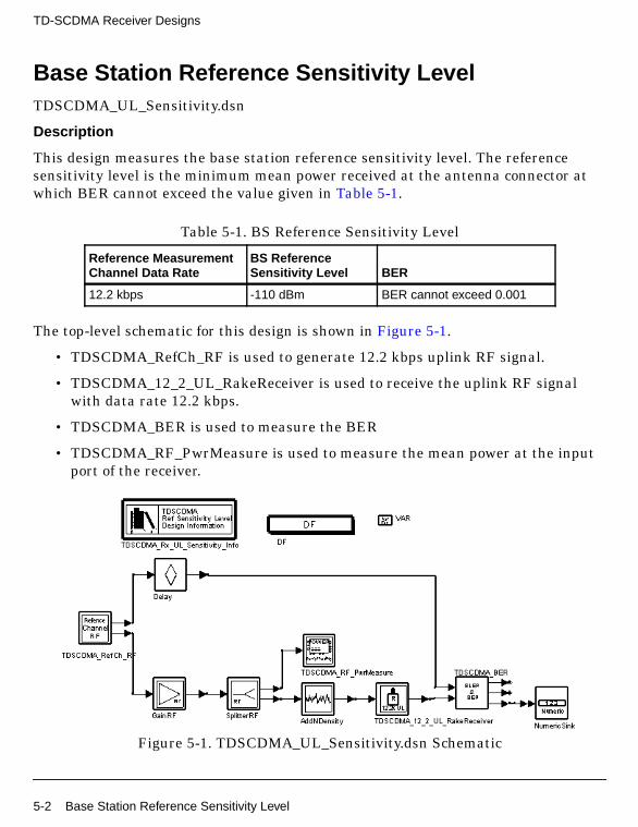
Base Station Reference Sensitivity LevelTDSCDMA_UL_Sensitivity.dsn
Description
This design measures the base station reference sensitivity level. The referencesensitivity level is the minimum mean power received at the antenna connector atwhich BER cannot exceed the value given in Table 5-1.
The top-level schematic for this design is shown in Figure 5-1.
• TDSCDMA_RefCh_RF is used to generate 12.2 kbps uplink RF signal.
• TDSCDMA_12_2_UL_RakeReceiver is used to receive the uplink RF signalwith data rate 12.2 kbps.
• TDSCDMA_BER is used to measure the BER
• TDSCDMA_RF_PwrMeasure is used to measure the mean power at the inputport of the receiver.
Figure 5-1. TDSCDMA_UL_Sensitivity.dsn Schematic
Table 5-1. BS Reference Sensitivity Level
Reference MeasurementChannel Data Rate
BS ReferenceSensitivity Level BER
12.2 kbps -110 dBm BER cannot exceed 0.001
5-2 Base Station Reference Sensitivity Level
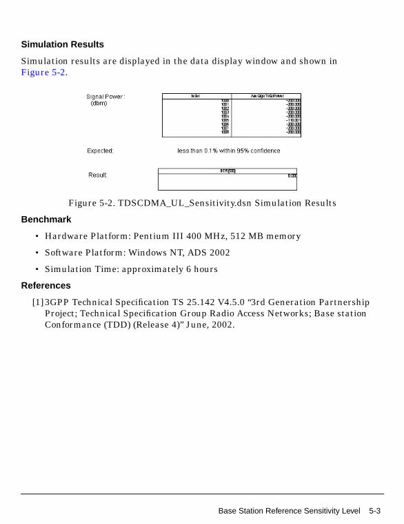
Simulation Results
Simulation results are displayed in the data display window and shown inFigure 5-2.
Figure 5-2. TDSCDMA_UL_Sensitivity.dsn Simulation Results
Benchmark
• Hardware Platform: Pentium III 400 MHz, 512 MB memory
• Software Platform: Windows NT, ADS 2002
• Simulation Time: approximately 6 hours
References
[1]3GPP Technical Specification TS 25.142 V4.5.0 “3rd Generation PartnershipProject; Technical Specification Group Radio Access Networks; Base stationConformance (TDD) (Release 4)” June, 2002.
Base Station Reference Sensitivity Level 5-3
TD-SCDMA Receiver Designs
User Equipment Adjacent Channel SelectivityTDSCDMA_DL_AdjacentChannel.dsn
Description
This design measures the adjacent channel selectivity. Adjacent channel selectivity isa measure of the receiver’s ability to receive a wanted signal at its assigned channelfrequency in the presence of an adjacent channel signal.
For the user equipment power class 2 and 3, the BER cannot exceed 0.001forparameters specified in Table 5-2. This test condition is equivalent to an adjacentchannel selectivity value of 33 dB.
The top-level schematic for this design is shown in Figure 5-3.
• The upper TDSCDMA_RefCh_RF is used to generate wanted 12.2 kbpsdownlink RF signal; the lower TDSCDMA_RefCh_RF is the adjacent channelsignal.
• TDSCDMA_12_2_DL_RakeReceiver is used to receive the wanted downlink RFsignal with a 12.2 kbps data rate in the presence of adjacent channel signal.
• TDSCDMA_BER is used to measure the BER.
• TDSCDMA_RF_PwrMeasure is used to measure the mean power at the inputport of the receiver.
Table 5-2. Test Parameters for Adjacent Channel Selectivity
Parameter Unit Level
dB 0
Ior dBm/1.28 MHz -91
Iosc dBm/1.28 MHz -54
Fuw offset MHz +1.6 or -1.6
ΣDPCH Ec–Ior
----------------------------------
5-4 User Equipment Adjacent Channel Selectivity
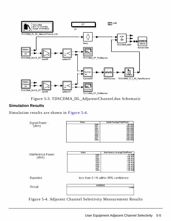
Figure 5-3. TDSCDMA_DL_AdjacentChannel.dsn Schematic
Simulation Results
Simulation results are shown in Figure 5-4.
Figure 5-4. Adjacent Channel Selectivity Measurement Results
User Equipment Adjacent Channel Selectivity 5-5
TD-SCDMA Receiver Designs
Benchmark
• Hardware Platform: Pentium III 450MHz, 512MB memory
• Software Platform: Windows 2000, ADS 2002
• Simulation Time: approximately 9 hours
References
[1] .3GPP TS 25.122 V4.4.0, “3rd Generation Partnership Project; TechnicalSpecification Group Radio Access Network; Terminal ConformanceSpecification; Radio transmission and Reception (TDD) (Release 4)”, June, 2002
5-6 User Equipment Adjacent Channel Selectivity
Chapter 6: TD-SCDMA Signal SourceDesigns
IntroductionThe TDSCDMA_SignalSource project demonstrates the special transientcharacteristics of TD-SCDMA signals from time and frequency domains, as well asrate matching calculation. Design examples in this project are described in thefollowing sections:
• Uplink signal characteristics: TDSCDMA_UL_Spectrum.dsn.
• Downlink signal characteristics: TDSCDMA_DL_ACLR.dsn.
• Rate matching calculator demonstration: TDSCDMA_RM_Cal_Demo.dsn
Introduction 6-1

TD-SCDMA Signal Source Designs
Uplink Signal CharacteristicsTDSCDMA_UL_Spectrum.dsn
Description
This design demonstrates user equipment out-of-band emissions; these are unwantedemissions immediately outside the nominal channel that result from the modulationprocess and non-linearity in the transmitter but excluding spurious emissions. Thisout-of-band emission limit is specified in terms of a spectrum emission mask andadjacent channel power.
The spectrum emission mask of the user equipment applies to carrier frequenciesthat are between 0.8 and 4.0 MHz. The out-of-channel emission is specified relative tothe user equipment output power measured in a 1.28 MHz bandwidth. The power ofany user equipment emission cannot exceed the levels specified in Table 6-1.
The top-level schematic for this design is shown in Figure 6-1.
• TDSCDMA_UL_RF generates a 12.2 kbps uplink RF signal source thatincludes one DPCH.
Table 6-1. Spectrum Emission Mask Requirements
f in MHz † Minimum Requirements Measurement Bandwidth
0.8 -35 dBc 30 kHz ††
0.8 - 1.8 30 kHz ††
1.8 - 2.4 30 kHz ††
2.4 - 4.0 -49 dBc 1 MHz †††
Notes:† f is the separation between the carrier frequency and the center of the measuring filter.†† The first and last measurement positions with a 30 kHz filter at f equals 0.815 and 2.385 MHz.††† The first and last measurement positions with a 1 MHz filter at f equals 2.9 and 3.5 MHz.The lower limit must be -55dBm/1.28MHz or the minimum requirement presented in this table,whichever is higher.
∆
35– 14 ∆fMHz-------------- 0.8–
–
dBc
49– 25 ∆fMHz-------------- 1.8–
–
dBc
∆∆∆
6-2 Uplink Signal Characteristics
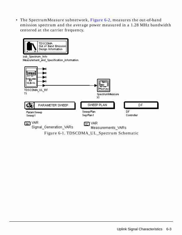
• The SpectrumMeasure subnetwork, Figure 6-2, measures the out-of-bandemission spectrum and the average power measured in a 1.28 MHz bandwidthcentered at the carrier frequency.
Figure 6-1. TDSCDMA_UL_Spectrum Schematic
Uplink Signal Characteristics 6-3
TD-SCDMA Signal Source Designs
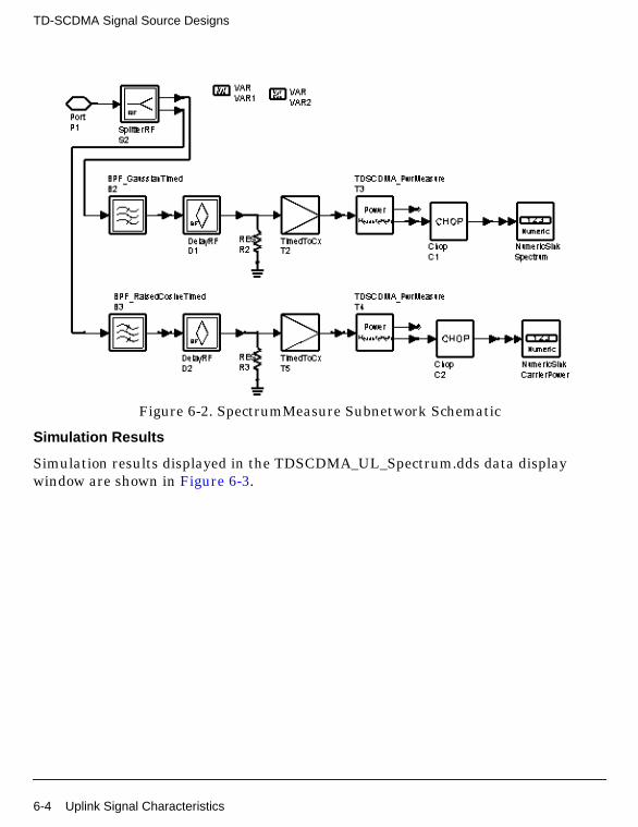
Figure 6-2. SpectrumMeasure Subnetwork Schematic
Simulation Results
Simulation results displayed in the TDSCDMA_UL_Spectrum.dds data displaywindow are shown in Figure 6-3.
6-4 Uplink Signal Characteristics
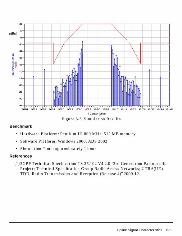
Figure 6-3. Simulation Results
Benchmark
• Hardware Platform: Pentium III 800 MHz, 512 MB memory
• Software Platform: Windows 2000, ADS 2002
• Simulation Time: approximately 1 hour
References
[1]3GPP Technical Specification TS 25.102 V4.2.0 “3rd Generation PartnershipProject; Technical Specification Group Radio Access Networks; UTRA(UE)TDD; Radio Transmission and Reception (Release 4)” 2000-12.
Uplink Signal Characteristics 6-5

TD-SCDMA Signal Source Designs
Adjacent Channel Power Leakage RatioTDSCDMA_DL_ACLR.dsn
Features
• ACLR measurements for TD-SCDMA downlink
• 12.2 kbps downlink reference measurement channel
• Roll-off α = 0.22 root raised-cosine filter
Description
This example measures ACLR for TD-SCDMA downlink.
The schematic for this design is shown in Figure 6-4. TDSCDMA_DL_RF generatesthe 12.2 kbps downlink reference channel for the measurement. TheSpectrumMeasure subnetwork implements average power measurement through aroot raised-cosine filter. By offsetting the center frequency of the root raised-cosinefilter, power leakage on the adjacent channel is measured.
Figure 6-4. TDSCDMA_DL_ACLR Schematic
6-6 Adjacent Channel Power Leakage Ratio
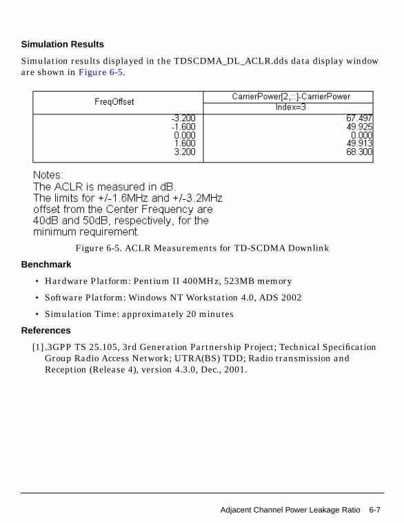
Simulation Results
Simulation results displayed in the TDSCDMA_DL_ACLR.dds data display windoware shown in Figure 6-5.
Figure 6-5. ACLR Measurements for TD-SCDMA Downlink
Benchmark
• Hardware Platform: Pentium II 400MHz, 523MB memory
• Software Platform: Windows NT Workstation 4.0, ADS 2002
• Simulation Time: approximately 20 minutes
References
[1] .3GPP TS 25.105, 3rd Generation Partnership Project; Technical SpecificationGroup Radio Access Network; UTRA(BS) TDD; Radio transmission andReception (Release 4), version 4.3.0, Dec., 2001.
Adjacent Channel Power Leakage Ratio 6-7

TD-SCDMA Signal Source Designs
Rate Match CalculatorTDSCDMA_RM_Cal_Demo.dsn
Description
This design demonstrates the use of TDSCDMA_RM_Cal rate matching calculatormodel. The puncture limit and rate match attributes are specified by users when theyconfigure TDSCDMA Design Library models related to rate matching.
In TDSCDMA specifications, frame sizes before and after rate matching are suppliedfor reference measurement channels only. TDSCDMA_RM_Cal calculates thepuncture limit and rate match attributes from the given frame sizes.
The schematic for this design is shown in Figure 6-6.
Figure 6-6. TDSCDMA_RM_Cal_Demo Schematic
Simulation Results
Simulation results displayed in TDSCDMA_RM_Cal_Demo.dds are shown inFigure 6-7.
6-8 Rate Match Calculator
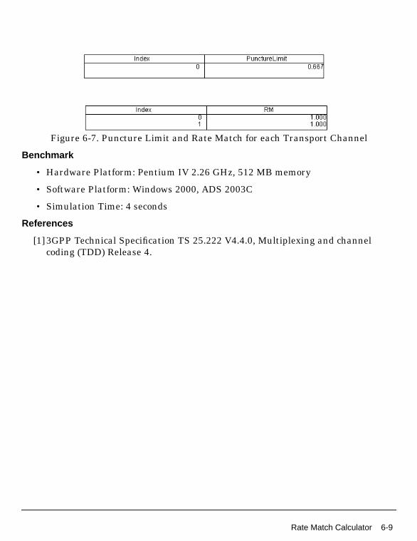
Figure 6-7. Puncture Limit and Rate Match for each Transport Channel
Benchmark
• Hardware Platform: Pentium IV 2.26 GHz, 512 MB memory
• Software Platform: Windows 2000, ADS 2003C
• Simulation Time: 4 seconds
References
[1]3GPP Technical Specification TS 25.222 V4.4.0, Multiplexing and channelcoding (TDD) Release 4.
Rate Match Calculator 6-9
TD-SCDMA Signal Source Designs
6-10 Rate Match Calculator

Chapter 7: TD-SCDMA Transmitter Designs
IntroductionThe TDSCDMA_Tx project demonstrates user equipment and base stationcharacteristics. Design examples in this project are described in the followingsections:
• Base station error vector magnitude: TDSCDMA_DL_EVM.dsn.
• User equipment code domain power: TDSCDMA_UL_CDP.dsn.
Introduction 7-1
TD-SCDMA Transmitter Designs
Base Station Error Vector MagnitudeTDSCDMA_DL_EVM.dsn
Description
This design demonstrates the base station error vector magnitude measurement todetermine the difference between the reference waveform and the measuredwaveform. This difference is called the error vector. Both waveforms pass through amatched root raised-cosine filter with a bandwidth corresponding to the consideredchip rate and roll-off a =0.22. Both waveforms are then further modified by selectingthe frequency, absolute phase, absolute amplitude and chip clock timing so as tominimize the error vector. The EVM result is defined as the square root of the ratio ofthe mean error vector power to the mean reference power expressed as a percentage.The measurement interval is one time slot. The error vector magnitude (EVM)cannot exceed 12.5%. The requirement is valid over the total power dynamic range asspecified in subclause 6.4.3 of TS 25.105.
The top-level schematic for this design is shown in Figure 7-1.
• TDSCDMA_DL_RF is used to generate a 12.2 kbps uplink RF signal.
• TDSCDMA_EVM is used to measure the EVM value of the RF signal. Thealgorithm is the same as that of VSA89600.
Figure 7-1. TDSCDMA_DL_EVM.dsn schematic
Simulation Results
Simulation results are shown in Figure 7-2.
7-2 Base Station Error Vector Magnitude
Figure 7-2. TDSCDMA_DL_EVM.dsn Simulation Results
Base Station Error Vector Magnitude 7-3
TD-SCDMA Transmitter Designs
Benchmark
• Hardware Platform: Pentium II 400 MHz, 512 MB memory
• Software Platform: Windows NT 4.0, ADS 2003A
• Simulation Time: 1 minute
References
[1]3GPP Technical Specification TS 25.142 V4.5.0 “3rd Generation PartnershipProject; Technical Specification Group Radio Access Networks; Base stationConformance (TDD) (Release 4)” June, 2002.
7-4 Base Station Error Vector Magnitude
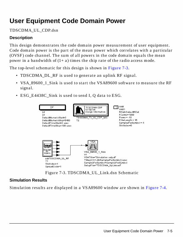
User Equipment Code Domain PowerTDSCDMA_UL_CDP.dsn
Description
This design demonstrates the code domain power measurement of user equipment.Code domain power is the part of the mean power which correlates with a particular(OVSF) code channel. The sum of all powers in the code domain equals the meanpower in a bandwidth of (1+ a) times the chip rate of the radio access mode.
The top-level schematic for this design is shown in Figure 7-3.
• TDSCDMA_DL_RF is used to generate an uplink RF signal.
• VSA_89600_1_Sink is used to start the VSA89600 software to measure the RFsignal.
• ESG_E4438C_Sink is used to send I, Q data to ESG.
Figure 7-3. TDSCDMA_UL_Link.dsn Schematic
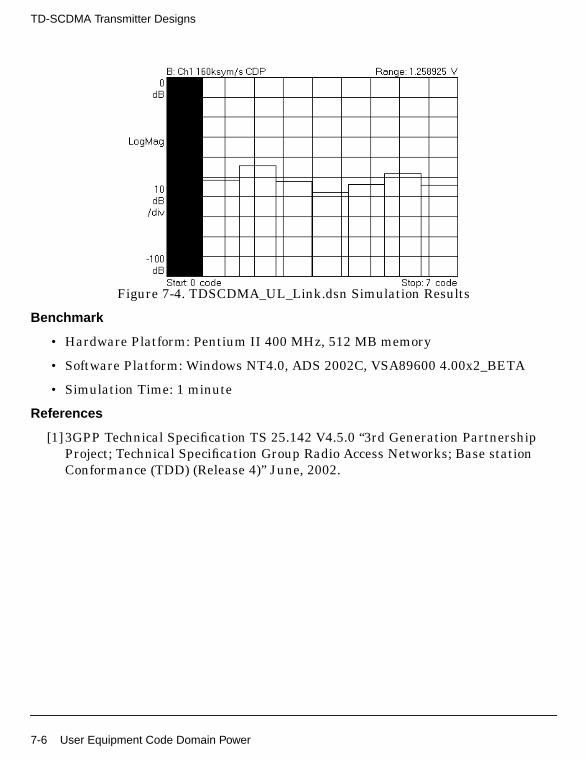
Simulation Results
Simulation results are displayed in a VSA89600 window are shown in Figure 7-4.
User Equipment Code Domain Power 7-5
TD-SCDMA Transmitter Designs
Figure 7-4. TDSCDMA_UL_Link.dsn Simulation Results
Benchmark
• Hardware Platform: Pentium II 400 MHz, 512 MB memory
• Software Platform: Windows NT4.0, ADS 2002C, VSA89600 4.00x2_BETA
• Simulation Time: 1 minute
References
[1]3GPP Technical Specification TS 25.142 V4.5.0 “3rd Generation PartnershipProject; Technical Specification Group Radio Access Networks; Base stationConformance (TDD) (Release 4)” June, 2002.
7-6 User Equipment Code Domain Power

Index
BBER performance, 2-1BLER performance, 2-1burst structure, 1-2Iinstrument links, 3-1
Jjoint detection receiver, 1-3
Pphysical layer, 1-1power amplifiers, 4-1
RRake receiver, 1-3receivers, 5-1
Ssignal sources, 6-1smart antenna, 1-1
TTD-SCDMA standard, 1-1time slots, 1-1transmitter structure, 1-2transmitters, 7-1
Uuplink synchronization, 1-1
Index-1

Index-2