The Design Process & ALU Design
55
Computer Architecture EECS 361 Lecture 5: The Design Process & ALU Design 361 design.1
-
Upload
khangminh22 -
Category
Documents
-
view
0 -
download
0
Transcript of The Design Process & ALU Design
Computer Architecture
EECS 361Lecture 5: The Design Process & ALU Design
361 design.1
Quick Review of Last Lecture
361 design.2

MIPS ISA Design Objectives and Implications
361 design.3
°Support general OS and C-style language needs
°Support general and embedded applications
°Use dynamic workload characteristics from general purpose program traces and SPECint to guide design decisions
°Implement processsor core with a relatively small number of gates
°Emphasize performance via fast clock
Traditional data types, common operations, typical addressing modes
RISC-style: Register-Register / Load-Store
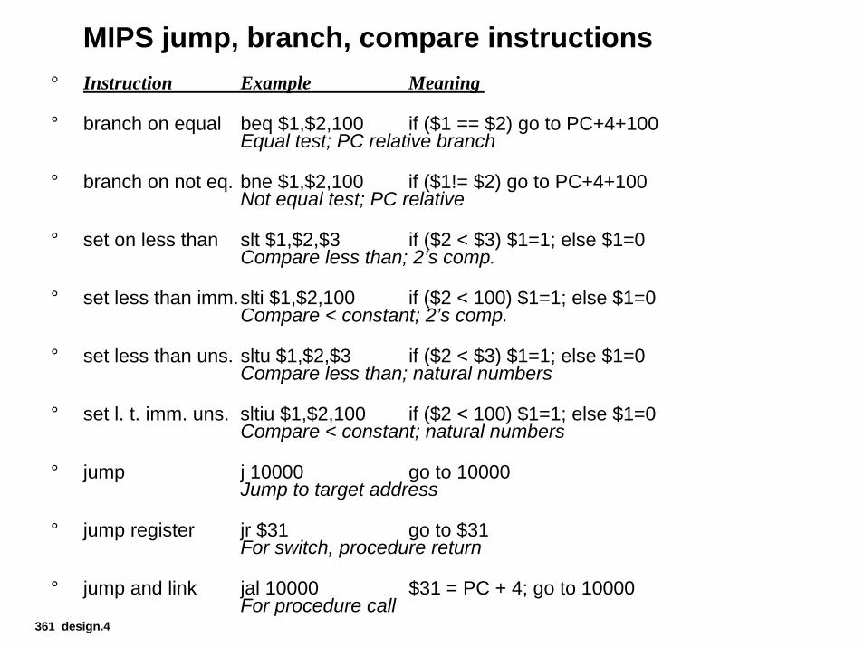
MIPS jump, branch, compare instructions
361 design.4
° Instruction Example Meaning
° branch on equal beq $1,$2,100 if ($1 == $2) go to PC+4+100Equal test; PC relative branch
° branch on not eq. bne $1,$2,100 if ($1!= $2) go to PC+4+100Not equal test; PC relative
° set on less than slt $1,$2,$3 if ($2 < $3) $1=1; else $1=0Compare less than; 2’s comp.
° set less than imm.slti $1,$2,100 if ($2 < 100) $1=1; else $1=0Compare < constant; 2’s comp.
° set less than uns. sltu $1,$2,$3 if ($2 < $3) $1=1; else $1=0Compare less than; natural numbers
° set l. t. imm. uns. sltiu $1,$2,100 if ($2 < 100) $1=1; else $1=0Compare < constant; natural numbers
° jump j 10000 go to 10000Jump to target address
° jump register jr $31 go to $31For switch, procedure return
° jump and link jal 10000 $31 = PC + 4; go to 10000For procedure call
Example: MIPS Instruction Formats and Addressing Modes
• All instructions 32 bits wide
op
361 design.5
6 5 5 5 11Register (direct) rs rt rd
register
immedop rs rtImmediate
Base+index immedop rs rt
register +
Memory
PC-relative immedop rs rt
PC +
Memory
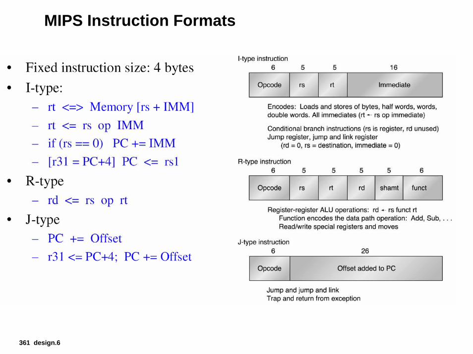
MIPS Instruction Formats
361 design.6
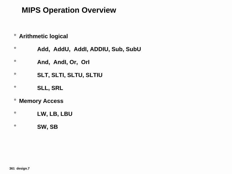
MIPS Operation Overview
361 design.7
° Arithmetic logical
° Add, AddU, AddI, ADDIU, Sub, SubU
° And, AndI, Or, OrI
° SLT, SLTI, SLTU, SLTIU
° SLL, SRL
° Memory Access
° LW, LB, LBU
° SW, SB
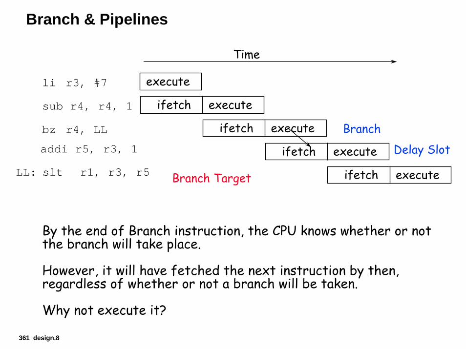
Branch & Pipelines
Time
361 design.8
execute
Branch
Delay Slot
Branch Target
ifetch execute
ifetch execute
ifetch executeLL: slt r1, r3, r5
li r3, #7
sub r4, r4, 1
bz r4, LL
addi r5, r3, 1
ifetch execute
By the end of Branch instruction, the CPU knows whether or not the branch will take place.
However, it will have fetched the next instruction by then, regardless of whether or not a branch will be taken.
Why not execute it?
361 design.9
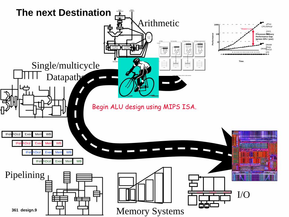
The next Destination
34-bit ALU
LO register(16x2 bits)
Load
HI
Cle
arH
I
Load
LO
MultiplicandRegister
ShiftAll
LoadMp
Extra2 bits
3232
LO[1:0]
Result[HI] Result[LO]
32 32
PrevLO
[1]
BoothE
ncoder ENC[0]
ENC[2]
"LO
[0]"
ControlLogic
InputMultiplier
32
Sub/Add
2
34
34
32
InputMultiplicand
32=>34signEx
34
34x2 MUX
32=>34signEx
<<1 34
ENC[1]
Multi x2/x1
2
2HI register(16x2 bits)
2
01
34 Arithmetic
Single/multicycleDatapaths
IFetchDcd Exec Mem WB
IFetchDcd Exec Mem WB
IFetchDcd Exec Mem WB
IFetchDcd Exec Mem WB
Pipelining
Memory Systems
I/O
µProc60%/yr.(2X/1.5yr)
DRAM9%/yr.(2X/10 yrs)1
10
100
1000
1 9 8 01 9 8 11 9 8 31 9 8 41 9 8 51 9 8 61 9 8 71 9 8 81 9 8 91 9 9 01 9 9 11 9 9 21 9 9 31 9 9 41 9 9 51 9 9 61 9 9 71 9 9 81 9 9 92 0 0 0
DRAM
CPU
1 9 8 2
Processor-MemoryPerformance Gap:(grows 50% / year)
Perf
orm
ance
Time
“Moore’s Law”
Begin ALU design using MIPS ISA.
Outline of Today’s Lecture
° An Overview of the Design Process
° Illustration using ALU design
° Refinements
361 design.10
The Design Process
"To Design Is To Represent"Design activity yields description/representation of an object
-- Traditional craftsman does not distinguish between the conceptualization and the artifact
-- Separation comes about because of complexity
-- The concept is captured in one or more representation languages
-- This process IS design
Design Begins With Requirements
-- Functional Capabilities: what it will do
-- Performance Characteristics: Speed, Power, Area, Cost, . . .
361 design.11
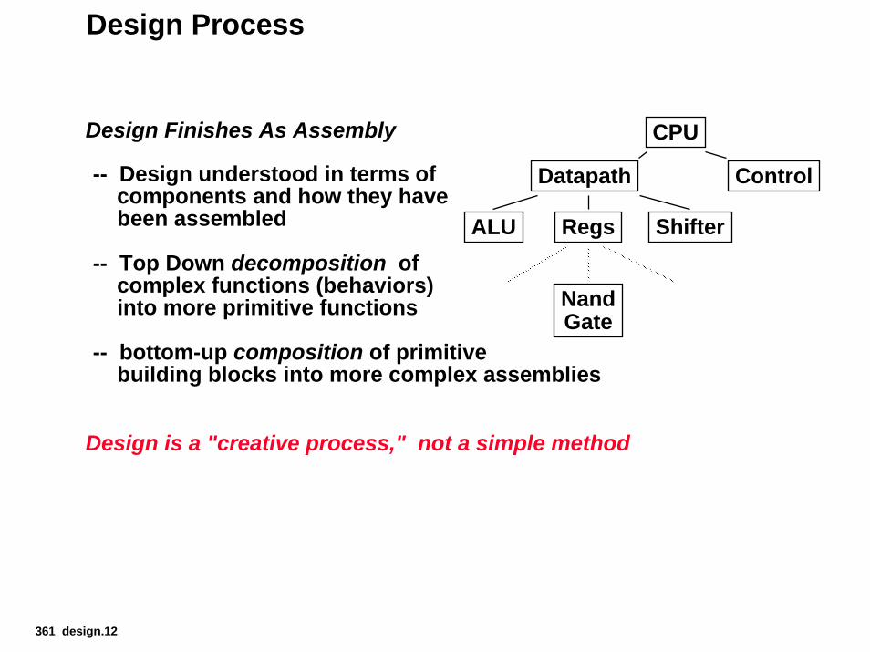
Design Process
Design Finishes As Assembly
-- Design understood in terms ofcomponents and how they havebeen assembled
-- Top Down decomposition ofcomplex functions (behaviors)into more primitive functions
-- bottom-up composition of primitivebuilding blocks into more complex assemblies
CPU
Datapath Control
ALU Regs Shifter
NandGate
Design is a "creative process," not a simple method
361 design.12
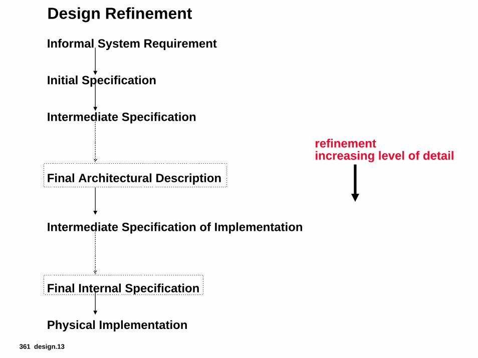
Design Refinement
361 design.13
Informal System Requirement
Initial Specification
Intermediate Specification
Final Architectural Description
Intermediate Specification of Implementation
Final Internal Specification
Physical Implementation
refinementincreasing level of detail
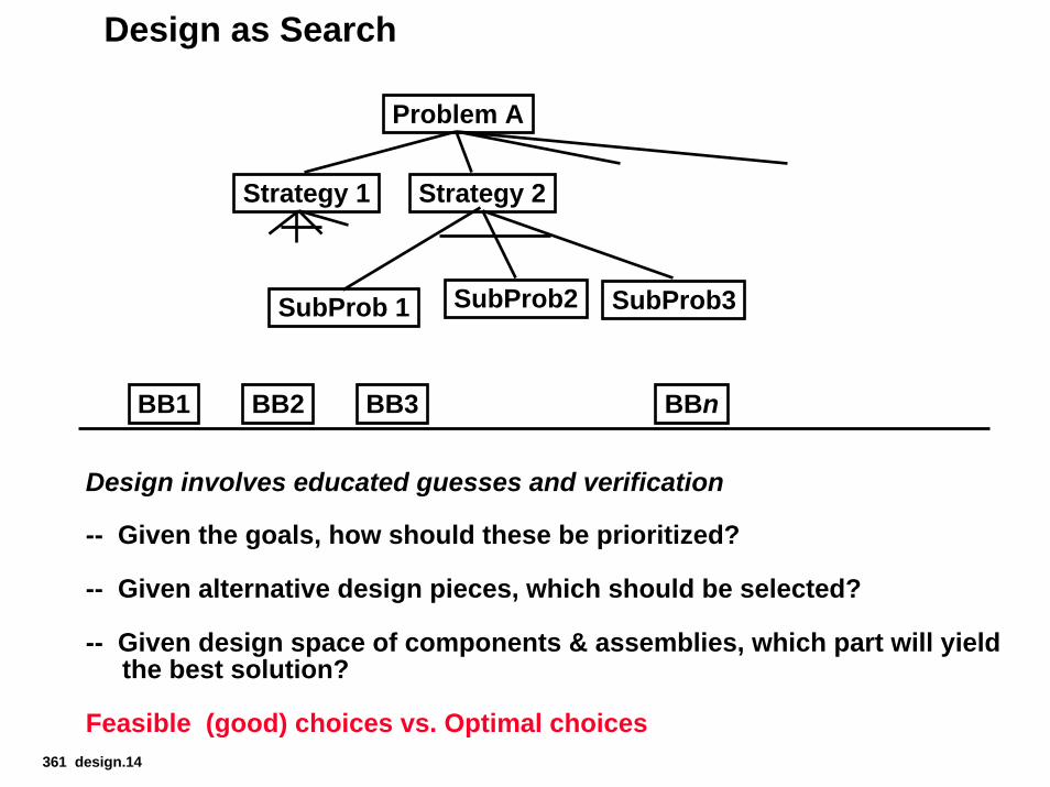
Design as Search
Problem A
Strategy 1 Strategy 2
SubProb 1 SubProb2 SubProb3
BB1 BB2 BB3 BBn
Design involves educated guesses and verification
-- Given the goals, how should these be prioritized?
-- Given alternative design pieces, which should be selected?
-- Given design space of components & assemblies, which part will yieldthe best solution?
Feasible (good) choices vs. Optimal choices361 design.14
Problem: Design a “fast” ALU for the MIPS ISA
° Requirements?
° Must support the Arithmetic / Logic operations
° Tradeoffs of cost and speed based on frequency of occurrence, hardware budget
361 design.15
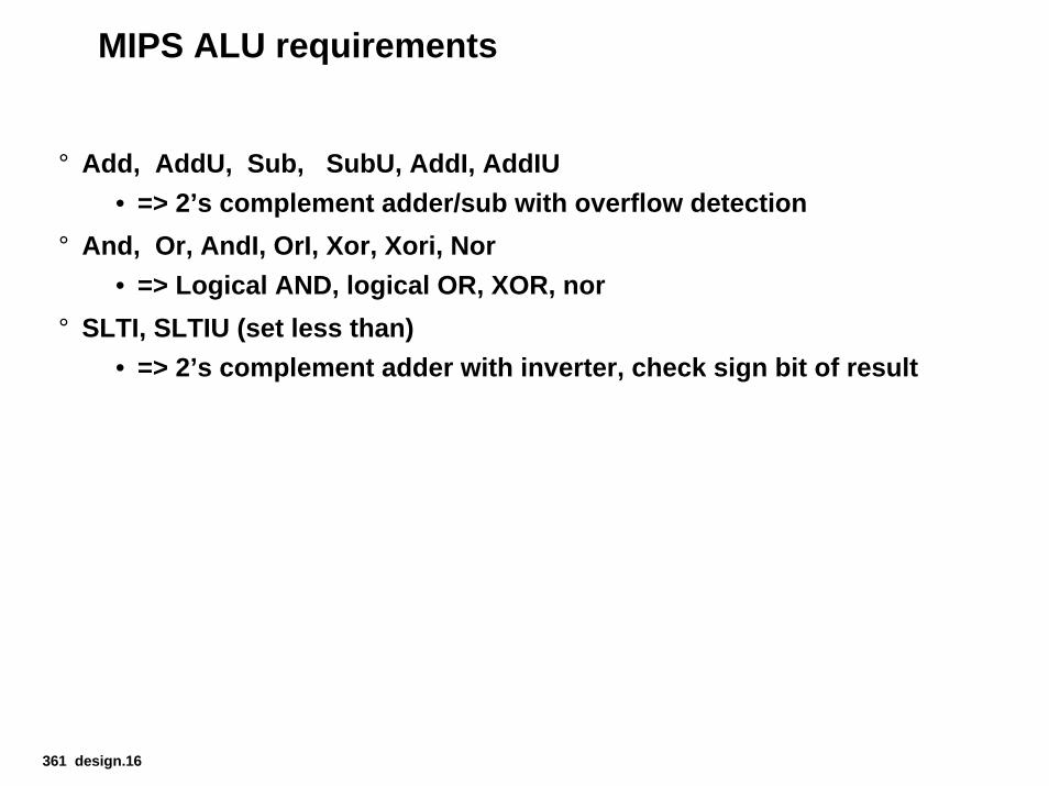
MIPS ALU requirements
361 design.16
° Add, AddU, Sub, SubU, AddI, AddIU• => 2’s complement adder/sub with overflow detection
° And, Or, AndI, OrI, Xor, Xori, Nor• => Logical AND, logical OR, XOR, nor
° SLTI, SLTIU (set less than)• => 2’s complement adder with inverter, check sign bit of result
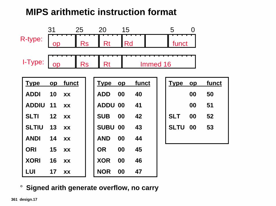
MIPS arithmetic instruction format
R-type:31 25 20 15 5 0
op Rs Rt Rd funct
I-Type: op Rs Rt Immed 16
Type op funct
ADDI 10 xx
ADDIU 11 xx
SLTI 12 xx
SLTIU 13 xx
ANDI 14 xx
ORI 15 xx
XORI 16 xx
LUI 17 xx
361 design.17
Type op funct
ADD 00 40
ADDU 00 41
SUB 00 42
SUBU 00 43
AND 00 44
OR 00 45
XOR 00 46
NOR 00 47
Type op funct
00 50
00 51
SLT 00 52
SLTU 00 53
° Signed arith generate overflow, no carry
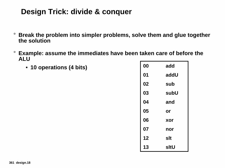
Design Trick: divide & conquer
° Break the problem into simpler problems, solve them and glue together the solution
° Example: assume the immediates have been taken care of before the ALU
• 10 operations (4 bits) 00 add
01 addU
02 sub
03 subU
04 and
05 or
06 xor
07 nor
12 slt
13 sltU
361 design.18
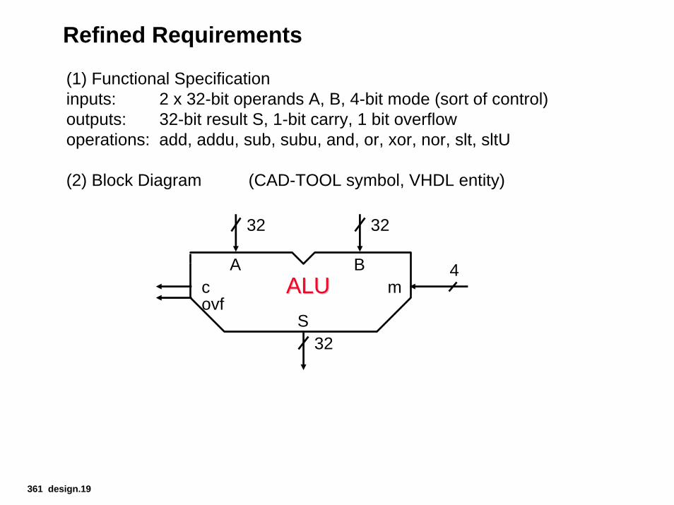
Refined Requirements
(1) Functional Specificationinputs: 2 x 32-bit operands A, B, 4-bit mode (sort of control)outputs: 32-bit result S, 1-bit carry, 1 bit overflowoperations: add, addu, sub, subu, and, or, xor, nor, slt, sltU
(2) Block Diagram (CAD-TOOL symbol, VHDL entity)
ALUALUA B
movf
S
32 32
32
4c
361 design.19
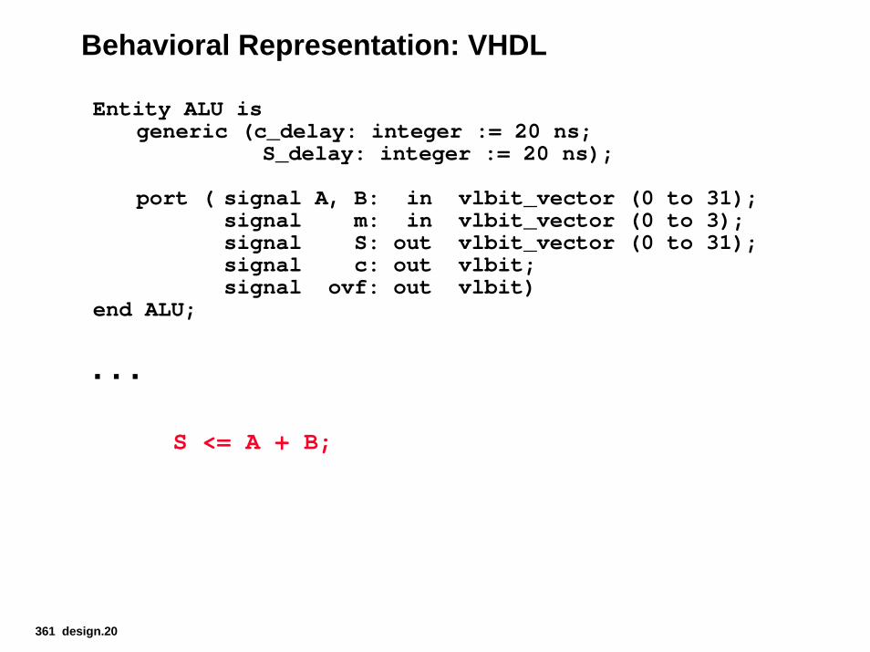
Behavioral Representation: VHDL
Entity ALU isgeneric (c_delay: integer := 20 ns;
S_delay: integer := 20 ns);
port ( signal A, B: in vlbit_vector (0 to 31);signal m: in vlbit_vector (0 to 3);signal S: out vlbit_vector (0 to 31);signal c: out vlbit;signal ovf: out vlbit)
end ALU;
. . .
S <= A + B;
361 design.20
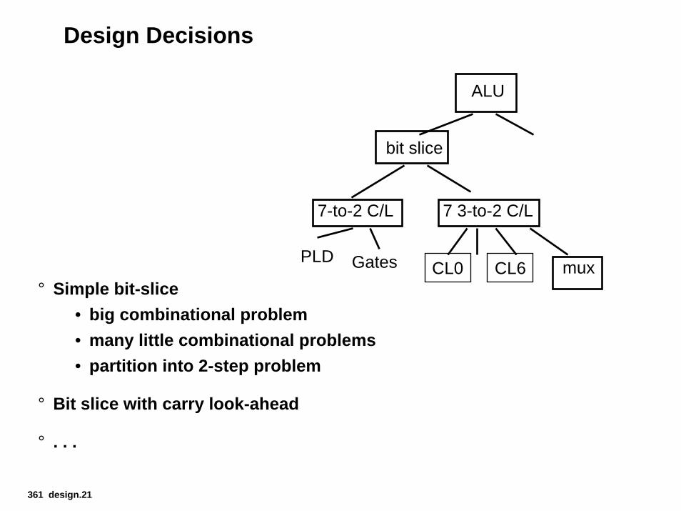
Design Decisions
° Simple bit-slice• big combinational problem• many little combinational problems• partition into 2-step problem
° Bit slice with carry look-ahead
° . . .
ALU
bit slice
7-to-2 C/L 7 3-to-2 C/L
PLD Gates muxCL0 CL6
361 design.21
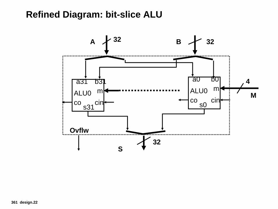
Refined Diagram: bit-slice ALU
A B
M
S
32 32
32
4
Ovflw
ALU0
a0 b0m
cincos0
ALU0
a31 b31m
cincos31
361 design.22
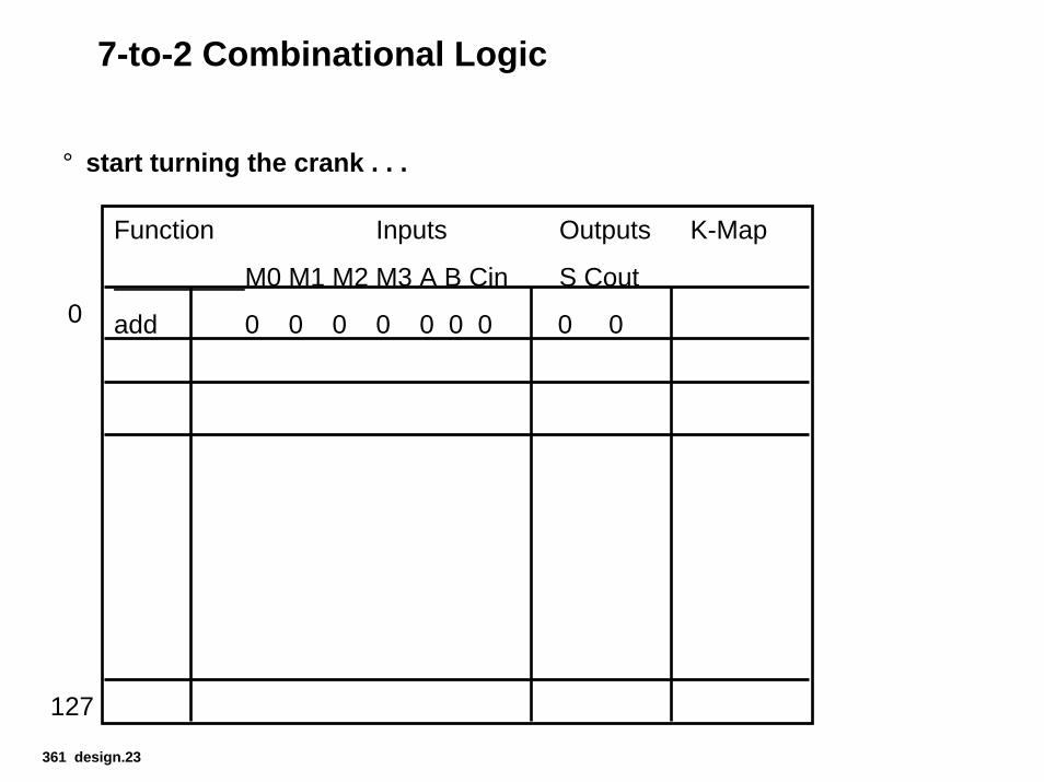
7-to-2 Combinational Logic
° start turning the crank . . .
Function Inputs Outputs K-Map
M0 M1 M2 M3 A B Cin S Cout
add 0 0 0 0 0 0 0 0 00
127
361 design.23
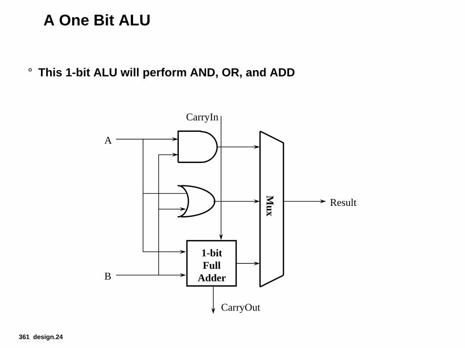
A One Bit ALU
° This 1-bit ALU will perform AND, OR, and ADD
A
B
1-bitFull
Adder
CarryOut
CarryIn
Mux Result
361 design.24
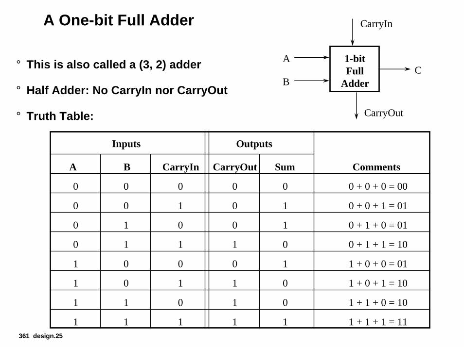
A One-bit Full Adder
1-bitFull
Adder
CarryOut
CarryIn
A
BC° This is also called a (3, 2) adder
° Half Adder: No CarryIn nor CarryOut
° Truth Table:
Inputs Outputs
CommentsA B CarryIn SumCarryOut
0 0 0 0 0 0 + 0 + 0 = 00
0 0 1 0 1 0 + 0 + 1 = 01
0 1 0 0 1 0 + 1 + 0 = 01
0 1 1 1 0 0 + 1 + 1 = 10
1 0 0 0 1 1 + 0 + 0 = 01
1 0 1 1 0 1 + 0 + 1 = 10
1 1 0 1 0 1 + 1 + 0 = 10
1 1 1 1 1 1 + 1 + 1 = 11361 design.25
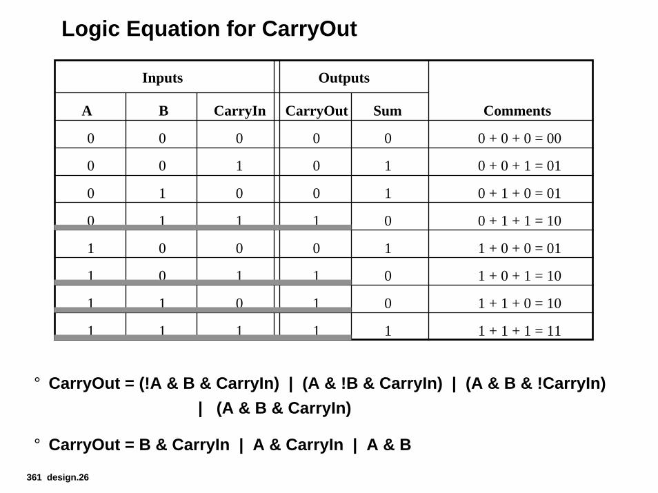
Logic Equation for CarryOut
Inputs Outputs
CommentsA B CarryIn SumCarryOut
0 0 0 0 0 0 + 0 + 0 = 00
0 0 1 0 1 0 + 0 + 1 = 01
0 1 0 0 1 0 + 1 + 0 = 01
0 1 1 1 0 0 + 1 + 1 = 10
1 0 0 0 1 1 + 0 + 0 = 01
1 0 1 1 0 1 + 0 + 1 = 10
1 1 0 1 0 1 + 1 + 0 = 10
1 1 1 1 1 1 + 1 + 1 = 11
° CarryOut = (!A & B & CarryIn) | (A & !B & CarryIn) | (A & B & !CarryIn)| (A & B & CarryIn)
° CarryOut = B & CarryIn | A & CarryIn | A & B
361 design.26
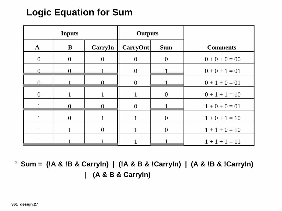
Logic Equation for Sum
Inputs Outputs
CommentsA B CarryIn SumCarryOut
0 0 0 0 0 0 + 0 + 0 = 00
0 0 1 0 1 0 + 0 + 1 = 01
0 1 0 0 1 0 + 1 + 0 = 01
0 1 1 1 0 0 + 1 + 1 = 10
1 0 0 0 1 1 + 0 + 0 = 01
1 0 1 1 0 1 + 0 + 1 = 10
1 1 0 1 0 1 + 1 + 0 = 10
1 1 1 1 1 1 + 1 + 1 = 11
° Sum = (!A & !B & CarryIn) | (!A & B & !CarryIn) | (A & !B & !CarryIn)| (A & B & CarryIn)
361 design.27
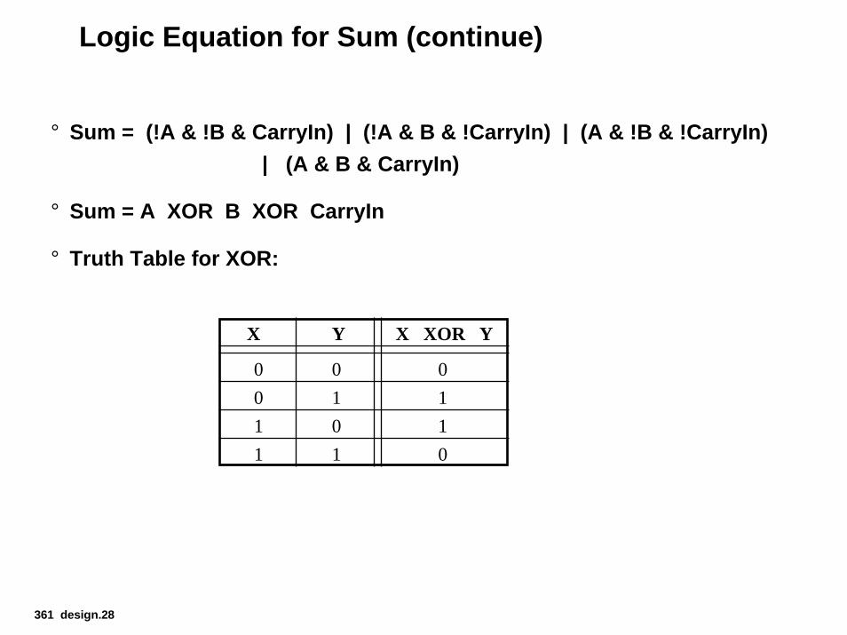
Logic Equation for Sum (continue)
° Sum = (!A & !B & CarryIn) | (!A & B & !CarryIn) | (A & !B & !CarryIn)| (A & B & CarryIn)
° Sum = A XOR B XOR CarryIn
° Truth Table for XOR:
X Y X XOR Y
0 0 00 1 11 0 11 1 0
361 design.28
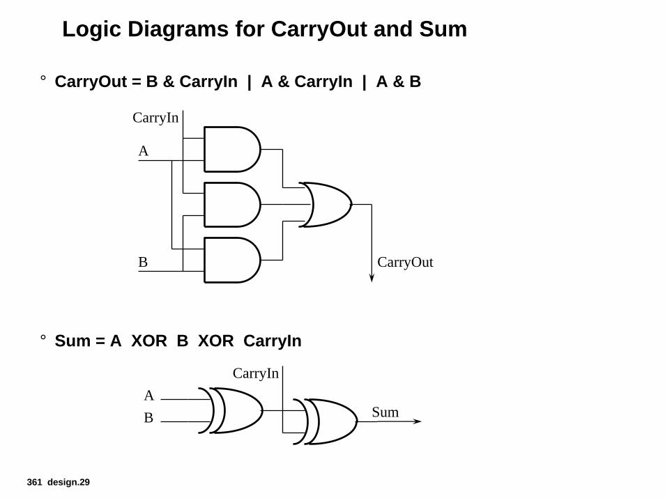
Logic Diagrams for CarryOut and Sum
° CarryOut = B & CarryIn | A & CarryIn | A & B
° Sum = A XOR B XOR CarryIn
CarryIn
CarryOut
A
B
AB
CarryIn
Sum
361 design.29
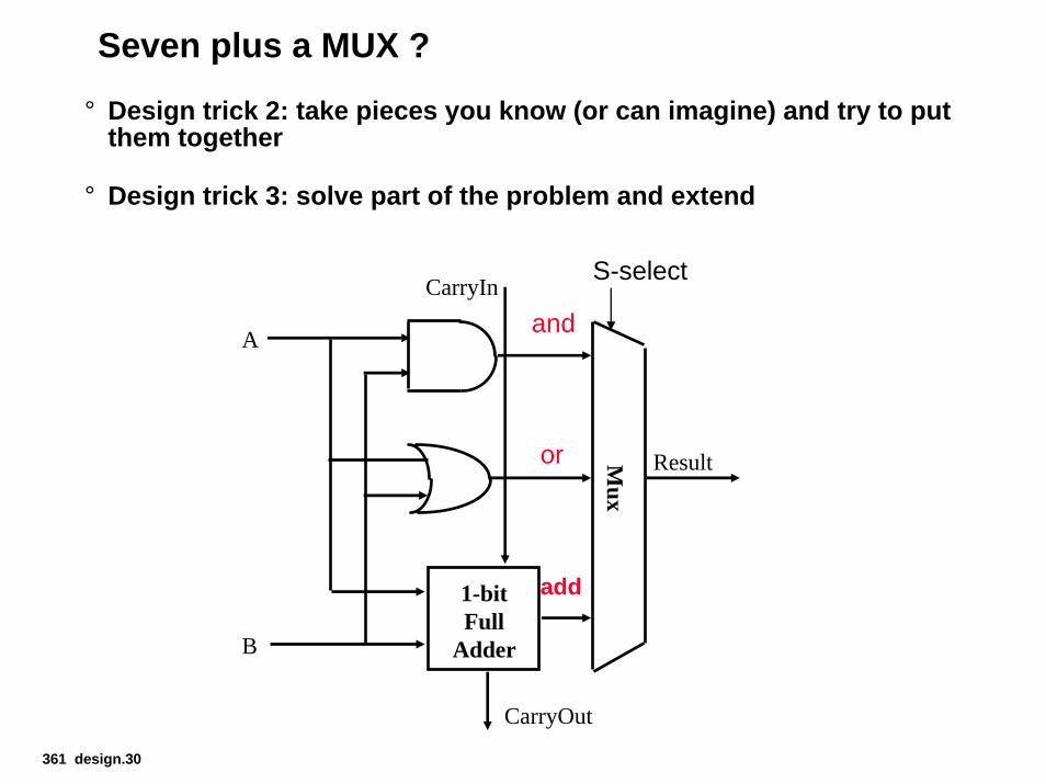
Seven plus a MUX ?
° Design trick 2: take pieces you know (or can imagine) and try to put them together
° Design trick 3: solve part of the problem and extend
361 design.30
A
B
1-bitFull
Adder
CarryOut
Mux
CarryIn
Result
add
and
or
S-select
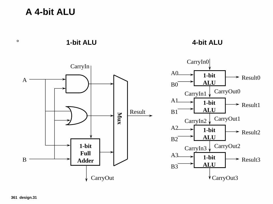
A 4-bit ALU
° 1-bit ALU 4-bit ALU
A0
B01-bitALU
Result0
CarryIn0
CarryOut0A1
B11-bitALU
Result1
CarryIn1
CarryOut1
A
B
1-bitFull
Adder
CarryOut
Mux
CarryIn
ResultCarryIn2
A2
B21-bitALU
Result2
CarryOut2A3
B31-bitALU
Result3
CarryIn3
CarryOut3
361 design.31
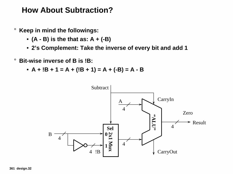
How About Subtraction?
° Keep in mind the followings:• (A - B) is the that as: A + (-B)• 2’s Complement: Take the inverse of every bit and add 1
° Bit-wise inverse of B is !B:• A + !B + 1 = A + (!B + 1) = A + (-B) = A - B
“AL
U”
4
4
4
A
!B
Result
Zero
CarryIn
CarryOut
4B
4
0
1
2x1 Mux
Sel
Subtract
361 design.32
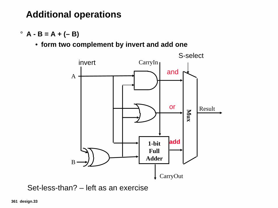
Additional operations
° A - B = A + (– B)• form two complement by invert and add one
A
B
1-bitFull
Adder
CarryOut
Mux
CarryIn
Result
add
and
or
S-selectinvert
Set-less-than? – left as an exercise361 design.33
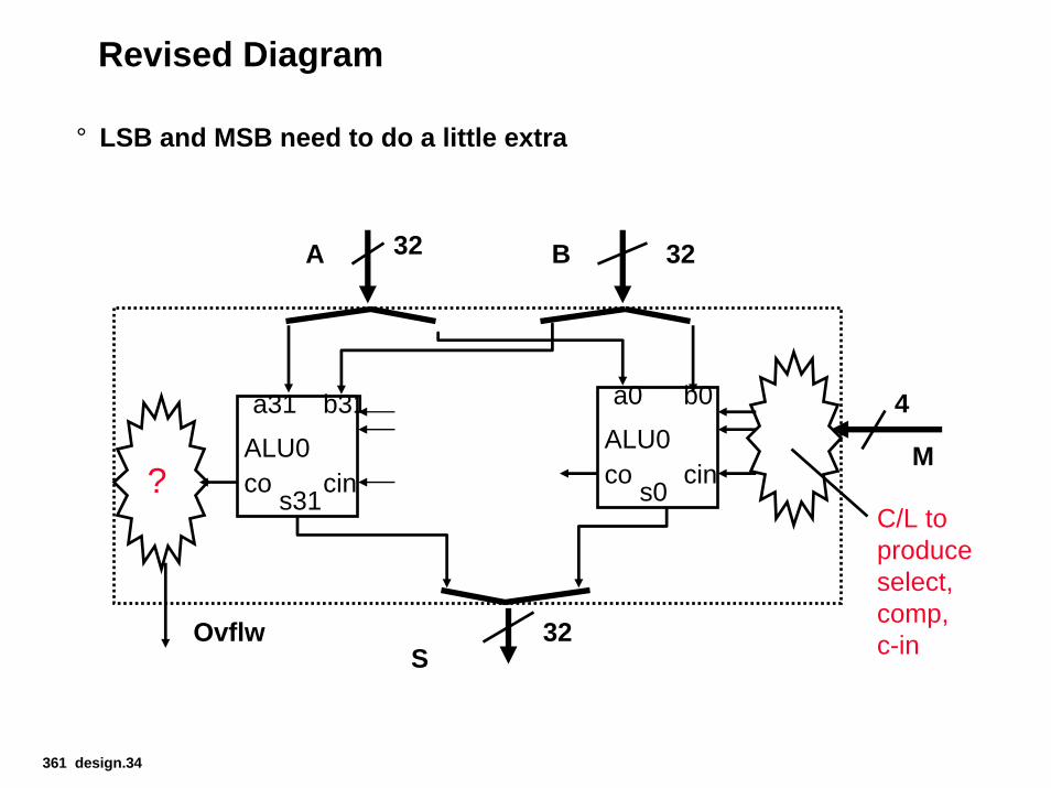
Revised Diagram
° LSB and MSB need to do a little extra
A B
M
S
32 32
32
4
Ovflw
ALU0
a0 b0
cincos0
ALU0
a31 b31
cincos31
C/L toproduceselect,comp,c-in
?
361 design.34
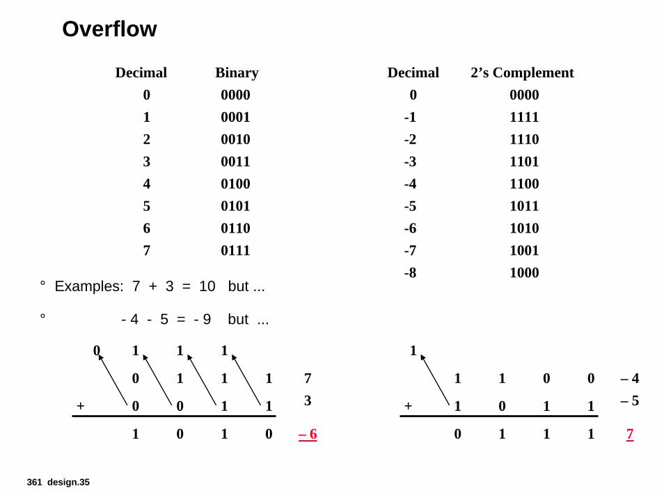
Overflow
Decimal0
-1-2-3-4-5-6-7-8
361 design.35
Decimal01234567
Binary00000001001000110100010101100111
2’s Complement000011111110110111001011101010011000
° Examples: 7 + 3 = 10 but ...
° - 4 - 5 = - 9 but ...
0 1 1 1
0 0 1 1+
1 0 1 0
1 110
1 1 0 0
1 0 1 1+
0 1 1 1
1
7 – 43 – 5
7– 6
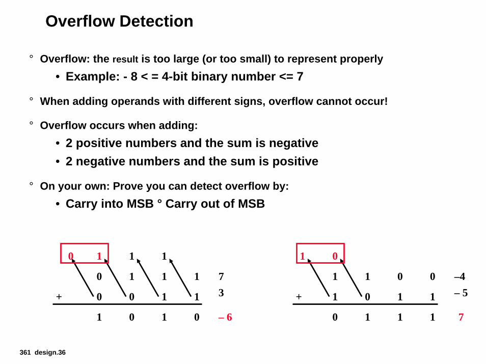
Overflow Detection
361 design.36
° Overflow: the result is too large (or too small) to represent properly• Example: - 8 < = 4-bit binary number <= 7
° When adding operands with different signs, overflow cannot occur!
° Overflow occurs when adding:• 2 positive numbers and the sum is negative• 2 negative numbers and the sum is positive
° On your own: Prove you can detect overflow by:• Carry into MSB ° Carry out of MSB
0 1 1 1
0 0 1 1+
1 0 1 0
1 1
1 1 0 0
1 0 1 1+
0 1 1 1
1 010
7 –4– 53
– 6 7
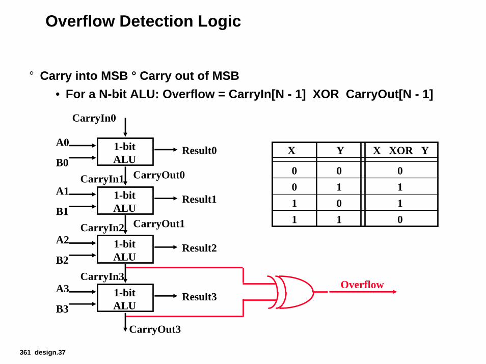
Overflow Detection Logic
° Carry into MSB ° Carry out of MSB• For a N-bit ALU: Overflow = CarryIn[N - 1] XOR CarryOut[N - 1]
A0
B01-bitALU
Result0
CarryIn0
CarryOut0A1
B11-bitALU
Result1
CarryIn1
CarryOut1A2
B21-bitALU
Result2
CarryIn2
A3
B31-bitALU
Result3
CarryIn3
CarryOut3
Overflow
X Y X XOR Y
0 0 00 1 11 0 11 1 0
361 design.37
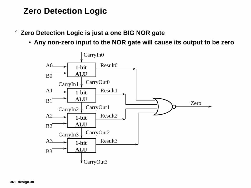
Zero Detection Logic
° Zero Detection Logic is just a one BIG NOR gate• Any non-zero input to the NOR gate will cause its output to be zero
CarryIn0
A0
B01-bitALU
Result0
CarryOut0A1
B11-bitALU
Result1CarryIn1
CarryOut1A2
B21-bitALU
Result2CarryIn2
CarryOut2A3
B31-bitALU
Result3CarryIn3
CarryOut3
Zero
361 design.38
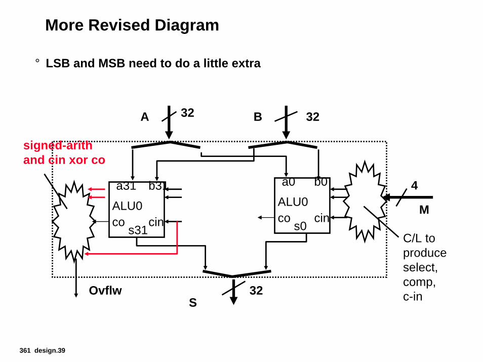
More Revised Diagram
° LSB and MSB need to do a little extra
A B
M
S
32 32
32
4
Ovflw
ALU0
a0 b0
cincos0
ALU0
a31 b31
cincos31
C/L toproduceselect,comp,c-in
signed-arithand cin xor co
361 design.39
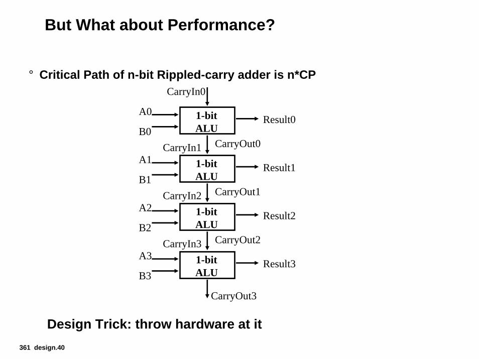
But What about Performance?
° Critical Path of n-bit Rippled-carry adder is n*CP
A0
B01-bitALU
Result0
CarryIn0
CarryOut0A1
B11-bitALU
Result1
CarryIn1
CarryOut1A2
B21-bitALU
Result2
CarryIn2
CarryOut2A3
B31-bitALU
Result3
CarryIn3
CarryOut3
Design Trick: throw hardware at it361 design.40
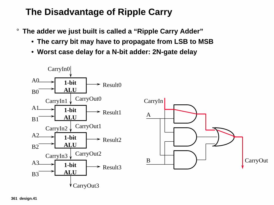
The Disadvantage of Ripple Carry
° The adder we just built is called a “Ripple Carry Adder”• The carry bit may have to propagate from LSB to MSB• Worst case delay for a N-bit adder: 2N-gate delay
361 design.41
A0
B01-bitALU
Result0
CarryOut0A1
B11-bitALU
Result1
CarryIn1
CarryOut1A2
B21-bitALU
Result2
CarryIn2
A3
B31-bitALU
Result3
CarryIn3
CarryOut3
CarryOut2
CarryIn0
CarryIn
CarryOut
A
B
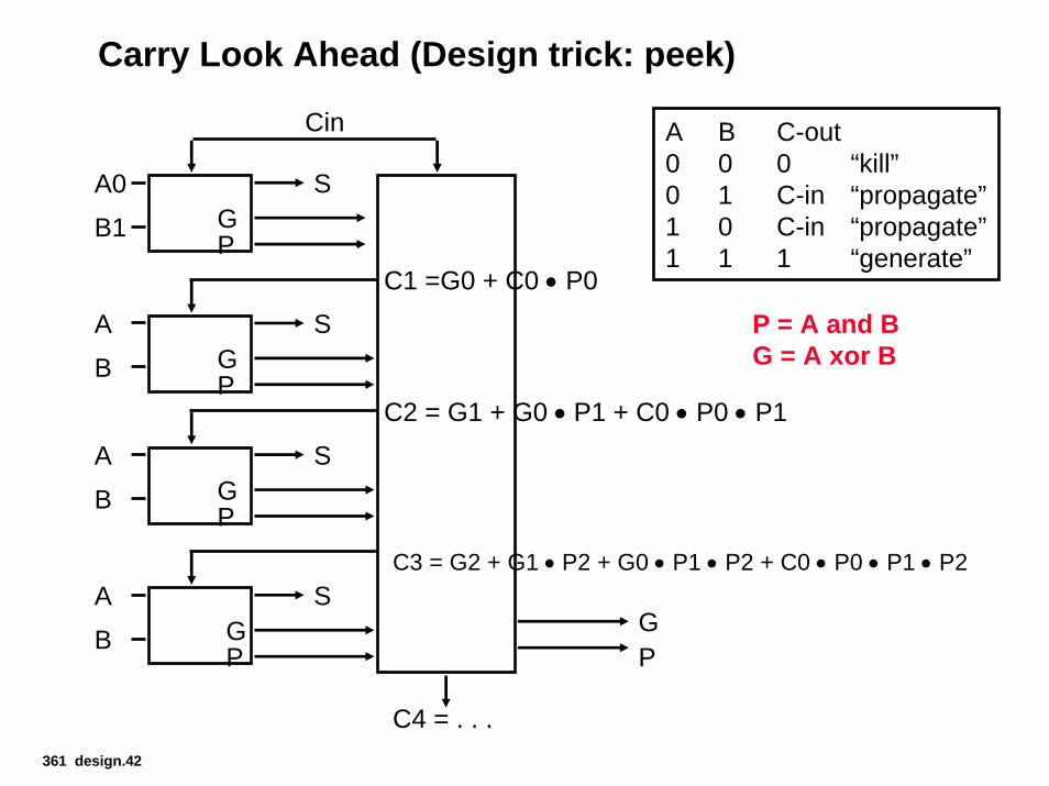
Carry Look Ahead (Design trick: peek)
A B C-out0 0 0 “kill”0 1 C-in “propagate”1 0 C-in “propagate”1 1 1 “generate”
A0
B1
SGP
P = A and BG = A xor B
A
B
SGP
A
B
SGP
A
B
SGP
Cin
C1 =G0 + C0 • P0
C2 = G1 + G0 • P1 + C0 • P0 • P1
C3 = G2 + G1 • P2 + G0 • P1 • P2 + C0 • P0 • P1 • P2
G
C4 = . . .
P
361 design.42
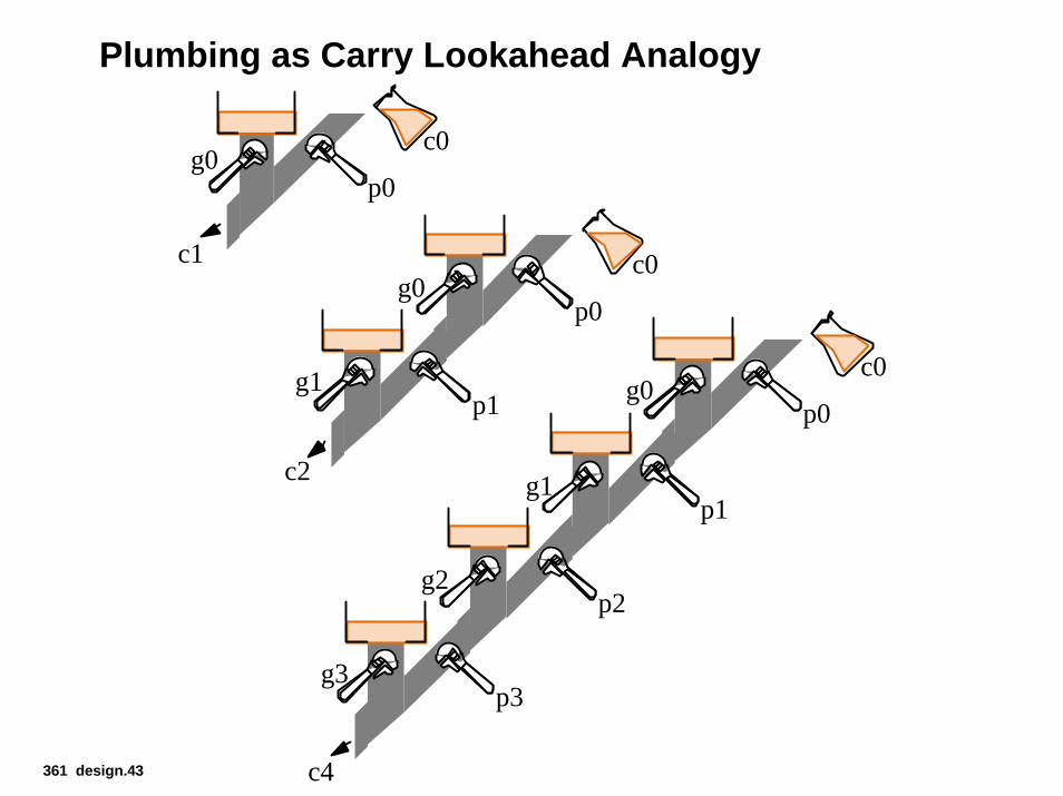
Plumbing as Carry Lookahead Analogy
p0
c0g0
c1
p0
c0g0
p1g1
c2
p0
c0g0
p1g1
p2g2
p3g3
c4361 design.43
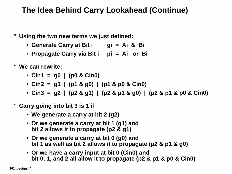
The Idea Behind Carry Lookahead (Continue)
361 design.44
° Using the two new terms we just defined:• Generate Carry at Bit i gi = Ai & Bi• Propagate Carry via Bit i pi = Ai or Bi
° We can rewrite:• Cin1 = g0 | (p0 & Cin0)• Cin2 = g1 | (p1 & g0) | (p1 & p0 & Cin0)• Cin3 = g2 | (p2 & g1) | (p2 & p1 & g0) | (p2 & p1 & p0 & Cin0)
° Carry going into bit 3 is 1 if• We generate a carry at bit 2 (g2)• Or we generate a carry at bit 1 (g1) and
bit 2 allows it to propagate (p2 & g1)• Or we generate a carry at bit 0 (g0) and
bit 1 as well as bit 2 allows it to propagate (p2 & p1 & g0) • Or we have a carry input at bit 0 (Cin0) and
bit 0, 1, and 2 all allow it to propagate (p2 & p1 & p0 & Cin0)
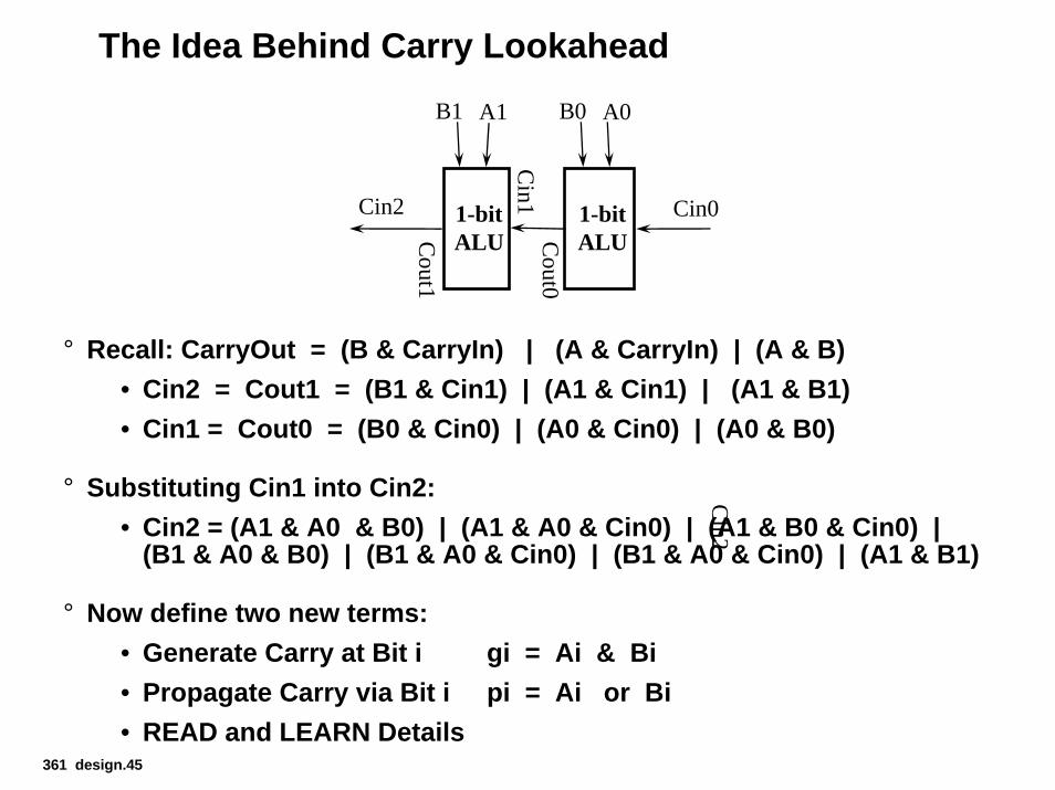
The Idea Behind Carry Lookahead
Cin0
A0B0
1-bitALUC
out0
A1B1
1-bitALU
Cin1
Cout1
Cin2
° Recall: CarryOut = (B & CarryIn) | (A & CarryIn) | (A & B)• Cin2 = Cout1 = (B1 & Cin1) | (A1 & Cin1) | (A1 & B1)• Cin1 = Cout0 = (B0 & Cin0) | (A0 & Cin0) | (A0 & B0)
° Substituting Cin1 into Cin2:• Cin2 = (A1 & A0 & B0) | (A1 & A0 & Cin0) | (A1 & B0 & Cin0) |
(B1 & A0 & B0) | (B1 & A0 & Cin0) | (B1 & A0 & Cin0) | (A1 & B1)
° Now define two new terms:• Generate Carry at Bit i gi = Ai & Bi• Propagate Carry via Bit i pi = Ai or Bi• READ and LEARN Details
Cin2
361 design.45
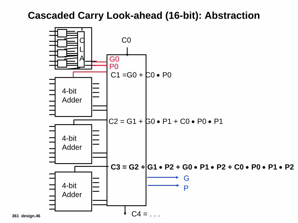
Cascaded Carry Look-ahead (16-bit): Abstraction
CLA
4-bitAdder
4-bitAdder
4-bitAdder
C1 =G0 + C0 • P0
C2 = G1 + G0 • P1 + C0 • P0 • P1
C3 = G2 + G1 • P2 + G0 • P1 • P2 + C0 • P0 • P1 • P2GP
G0P0
C4 = . . .
C0
361 design.46
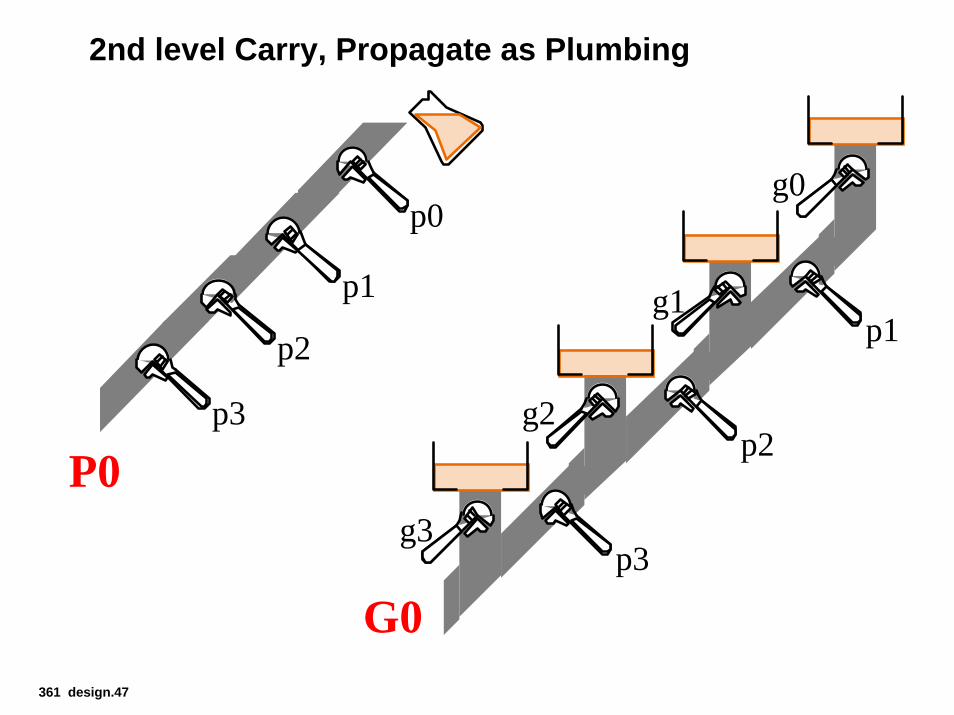
2nd level Carry, Propagate as Plumbing
p0g0
p1g1
p2g2
p3g3
G0
p1
p2
p3
P0
361 design.47
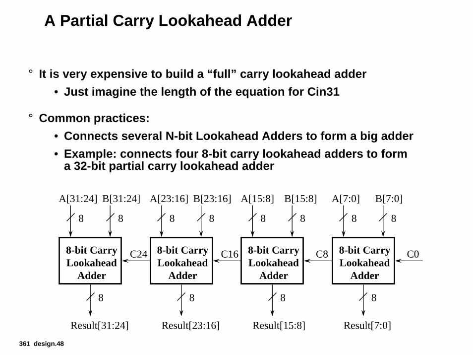
A Partial Carry Lookahead Adder
361 design.48
° It is very expensive to build a “full” carry lookahead adder• Just imagine the length of the equation for Cin31
° Common practices:• Connects several N-bit Lookahead Adders to form a big adder• Example: connects four 8-bit carry lookahead adders to form
a 32-bit partial carry lookahead adder
8-bit CarryLookahead
Adder
C0
8
88
Result[7:0]
B[7:0]A[7:0]
8-bit CarryLookahead
Adder
C8
8
88
Result[15:8]
B[15:8]A[15:8]
8-bit CarryLookahead
Adder
C16
8
88
Result[23:16]
B[23:16]A[23:16]
8-bit CarryLookahead
Adder
C24
8
88
Result[31:24]
B[31:24]A[31:24]
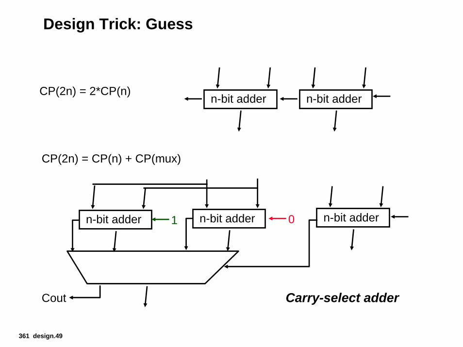
Design Trick: Guess
n-bit adder n-bit adderCP(2n) = 2*CP(n)
CP(2n) = CP(n) + CP(mux)
361 design.49
n-bit adder n-bit addern-bit adder 1 0
Cout Carry-select adder
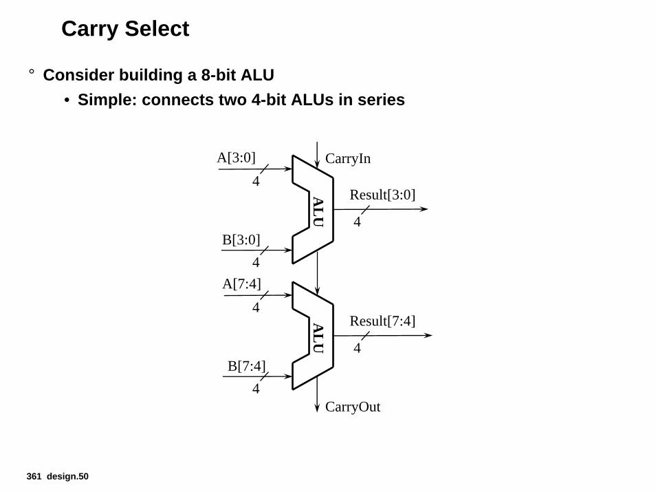
Carry Select
° Consider building a 8-bit ALU• Simple: connects two 4-bit ALUs in series
Result[3:0]AL
U
4
4
4
A[3:0] CarryIn
B[3:0]
AL
U
4
4
4
A[7:4]
Result[7:4]
CarryOut
B[7:4]
361 design.50
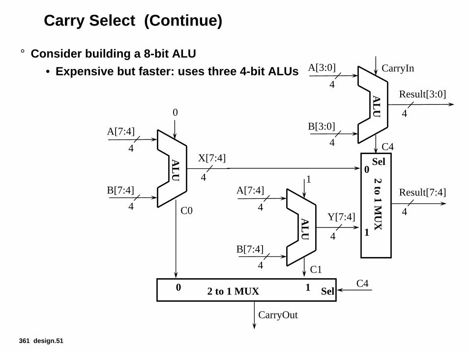
Carry Select (Continue)
° Consider building a 8-bit ALU• Expensive but faster: uses three 4-bit ALUs
Result[3:0]AL
U4
4
4
A[3:0] CarryIn
B[3:0]
C4
4
X[7:4]AL
U
4
4
A[7:4]
0
B[7:4]
C0
4
Y[7:4]AL
U
4
4
A[7:4]1
B[7:4]
C1
2 to 1 MU
X
Sel0
1
Result[7:4]
4
2 to 1 MUX0 1 SelC4
CarryOut
361 design.51
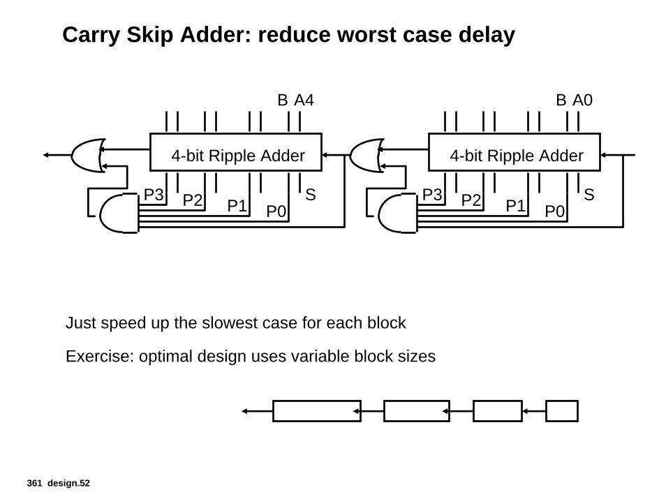
Carry Skip Adder: reduce worst case delay
4-bit Ripple Adder
A0B
SP0P1P2P3
4-bit Ripple Adder
A4B
SP0P1P2P3
361 design.52
Just speed up the slowest case for each block
Exercise: optimal design uses variable block sizes
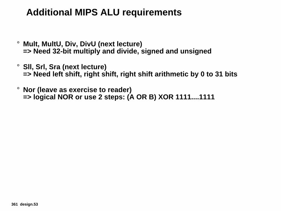
Additional MIPS ALU requirements
° Mult, MultU, Div, DivU (next lecture)=> Need 32-bit multiply and divide, signed and unsigned
° Sll, Srl, Sra (next lecture)=> Need left shift, right shift, right shift arithmetic by 0 to 31 bits
° Nor (leave as exercise to reader)=> logical NOR or use 2 steps: (A OR B) XOR 1111....1111
361 design.53
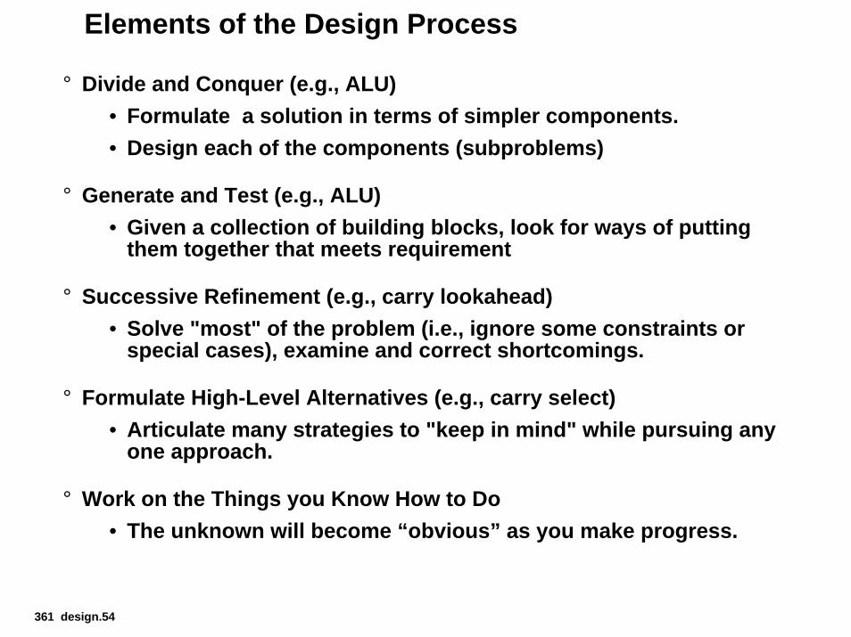
Elements of the Design Process
361 design.54
° Divide and Conquer (e.g., ALU)• Formulate a solution in terms of simpler components.• Design each of the components (subproblems)
° Generate and Test (e.g., ALU)• Given a collection of building blocks, look for ways of putting
them together that meets requirement
° Successive Refinement (e.g., carry lookahead)• Solve "most" of the problem (i.e., ignore some constraints or
special cases), examine and correct shortcomings.
° Formulate High-Level Alternatives (e.g., carry select)• Articulate many strategies to "keep in mind" while pursuing any
one approach.
° Work on the Things you Know How to Do• The unknown will become “obvious” as you make progress.
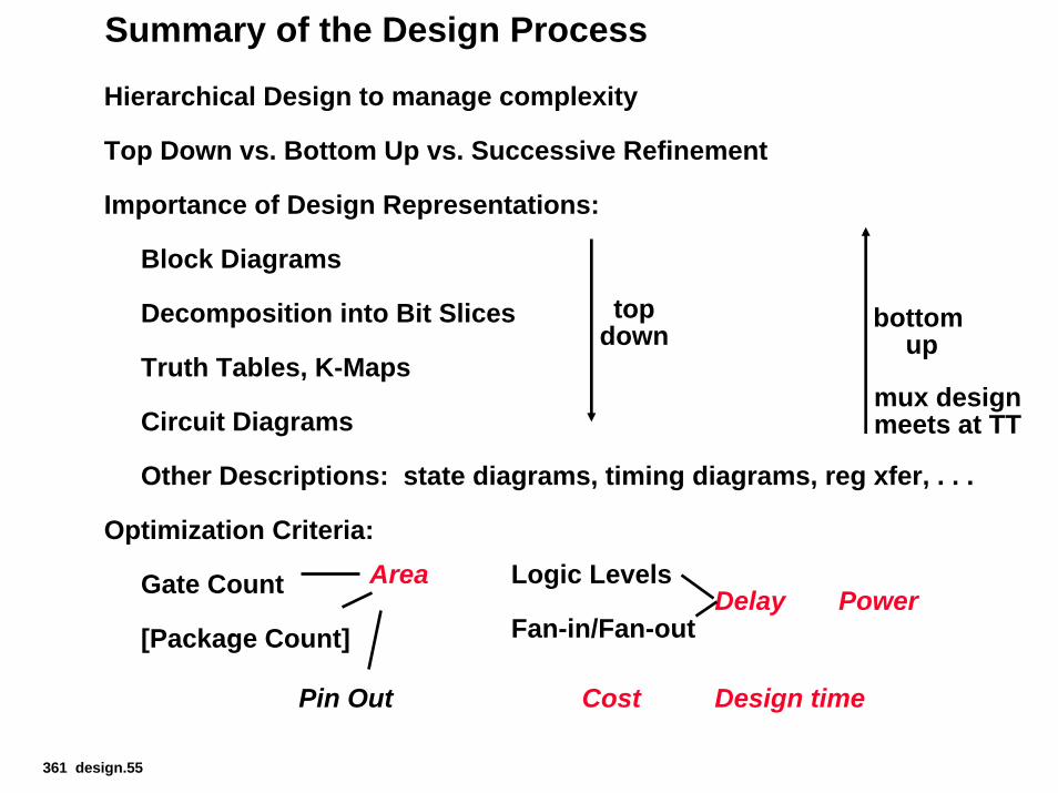
Summary of the Design Process
Hierarchical Design to manage complexity
Top Down vs. Bottom Up vs. Successive Refinement
Importance of Design Representations:
Block Diagrams
Decomposition into Bit Slices
Truth Tables, K-Maps
Circuit Diagrams
Other Descriptions: state diagrams, timing diagrams, reg xfer, . . .
Optimization Criteria:
Gate Count
[Package Count]
Logic Levels
Fan-in/Fan-outPower
topdown bottom
up
AreaDelay
mux designmeets at TT
Cost Design timePin Out
361 design.55