
Delay Optimization and Power Optimization of 4-Bit ALU ...
12
SMART MOVES JOURNAL IJOSCIENCE ISSN NO: 2582-4600 VOL. 6, ISSUE 2, FEBRUARY 2020 DOI: https://doi.org/10.24113/ijoscience.v6i2.264 www.ijoscience.com 1 Delay Optimization and Power Optimization of 4-Bit ALU Designed in FS-GDI Technique Rimjhim Saxena Kiran Sharma M. Tech. Scholar Assit. Professor SAM College of Science and Technology Bhopal, M.P, India SAM College of Science and Technology Bhopal, M.P, India [email protected] [email protected] Abstract-In this thesis proposed a reduction of delay, leakage current, leakage power. First find out the leakage current and leakage power. This thesis uses a gate diffusion input technique. By using this no of transistor is reduced. If number of transistor is reduced, area is also reduced, leakage current also affected. To study all parameter in this thesis uses a 2x1 MUX, 4x1MUX,16x1 MUX and ALU. Applying a GDI technique and also implemented by using a CMOS technique. Then do comparisons on GDI and CMOS technique and do a capacitance calculation. To implement all those things use a microwind 3.1 and DSCH 2.0. It is an Electronic Design Automation (EDA) environment that allows implementing a integrating in a single framework different applications and tools, allowing supporting all the stages of IC design and verification from a single environment. The resulting layout must verify some geometric rules dependent on the technology (design rules). Now checked with a Design Rule Checker (DRC) to find any error in the layout diagram and them simulation is performed. In implementing and do a comparisons of GDI and CMOS technique we get a 75% advantage in 2x1 MUX in counting the number of transistor. In 4x1 MUX we get again a 75% gain in the number of transistor. In 8x1 MUX, give a 78% benefits in the number of transistor. In 16x1 MUX, give a 81% benefits in the number of transistor. In 1 bit ALU give a 54% benefits in the number of transistor. If related power consumption, get a 74% benefits in comparisons of GDI and CMOS technique in 2x1 MUX. In 4x1mux give the advantage of 79% in the power consumption in comparisons of GDI and CMOS technique. In 8x1mux give the advantage of 78% in the power consumption in comparisons of GDI and CMOS technique. In 16x1mux give the advantage of 79% in the power consumption comparisons of GDI and CMOS technique. In bit ALU give the advantage of 64% in the power consumption in comparisons of GDI and CMOS technique. I.INTRODUCTION Reducing power losses in VLSI circuits is becoming one of the most significant challenges in the semiconductor industry. Performance optimization techniques are applied to all semiconductor design levels. Advanced processors offer numerous architectural improvements, such as branch forecasting, software hardware co- optimization, and the use of multiple cores in a single processor [3]. Portability requirements for laptops and other portable devices significantly limit size and power consumption. Although battery technology is constantly improving and processors and displays are improving rapidly in terms of power consumption, battery life and weight are factors that have a significant impact on the way laptops can be used for. These devices often require real-time processing functions and therefore require high throughput.[4] Energy consumption becomes the limiting factor for the range of functions of these devices. The wider and continuous use of network services will only exaggerate this problem because communication consumes a relatively high amount of energy. The gradual downsizing of the technology has led to the use of lower supply voltages for CMOS circuits, which affects lower threshold voltages to improve performance [5]. As the channel length decreases for future technology generations, the threshold voltage and gate oxide thickness are also reduced to keep pace with performance [6,7]. A lower threshold voltage leads to an exponential increase in the leakage current because the transistors cannot be completely turned off. In a CMOS circuit, total power loss includes dynamic and static components. The components of static power loss are losses below the threshold, junction losses, gate oxide losses, network- induced drainage losses and breakage losses.[8,9] This applies to directly battery-powered portable devices such as cell phones and PDAs, as they have a long service life. Different techniques used to effectively minimize this power loss. Stack Keeper is a technique for reducing losses. Leaks are a serious problem, especially for CMOS circuits in NANO-scale technology [10]. II.LITERATURE REVIEW Kaushik Roy et. to the. This results in a high leakage current in the deep sub-micrometric range and contributes significantly to the power loss of the CMOS circuits since
-
Upload
khangminh22 -
Category
Documents
-
view
3 -
download
0
Transcript of Delay Optimization and Power Optimization of 4-Bit ALU ...
SMART MOVES JOURNAL IJOSCIENCE ISSN NO: 2582-4600 VOL. 6, ISSUE 2, FEBRUARY 2020
DOI: https://doi.org/10.24113/ijoscience.v6i2.264
www.ijoscience.com 1
Delay Optimization and Power Optimization
of 4-Bit ALU Designed in FS-GDI Technique
Rimjhim Saxena
Kiran Sharma
M. Tech. Scholar Assit. Professor
SAM College of Science and Technology
Bhopal, M.P, India
SAM College of Science and Technology
Bhopal, M.P, India
[email protected] [email protected]
Abstract-In this thesis proposed a reduction of delay,
leakage current, leakage power. First find out the leakage
current and leakage power. This thesis uses a gate diffusion
input technique. By using this no of transistor is reduced. If
number of transistor is reduced, area is also reduced,
leakage current also affected.
To study all parameter in this thesis uses a 2x1 MUX,
4x1MUX,16x1 MUX and ALU. Applying a GDI technique
and also implemented by using a CMOS technique. Then do
comparisons on GDI and CMOS technique and do a
capacitance calculation.
To implement all those things use a microwind 3.1 and
DSCH 2.0. It is an Electronic Design Automation (EDA)
environment that allows implementing a integrating in a
single framework different applications and tools, allowing
supporting all the stages of IC design and verification from
a single environment. The resulting layout must verify some
geometric rules dependent on the technology (design rules).
Now checked with a Design Rule Checker (DRC) to find any
error in the layout diagram and them simulation is
performed.
In implementing and do a comparisons of GDI and CMOS
technique we get a 75% advantage in 2x1 MUX in counting
the number of transistor. In 4x1 MUX we get again a 75%
gain in the number of transistor. In 8x1 MUX, give a 78%
benefits in the number of transistor. In 16x1 MUX, give a
81% benefits in the number of transistor. In 1 bit ALU give
a 54% benefits in the number of transistor.
If related power consumption, get a 74% benefits in
comparisons of GDI and CMOS technique in 2x1 MUX. In
4x1mux give the advantage of 79% in the power
consumption in comparisons of GDI and CMOS technique.
In 8x1mux give the advantage of 78% in the power
consumption in comparisons of GDI and CMOS technique.
In 16x1mux give the advantage of 79% in the power
consumption comparisons of GDI and CMOS technique. In
bit ALU give the advantage of 64% in the power
consumption in comparisons of GDI and CMOS technique.
I.INTRODUCTION
Reducing power losses in VLSI circuits is becoming one
of the most significant challenges in the semiconductor
industry. Performance optimization techniques are
applied to all semiconductor design levels. Advanced
processors offer numerous architectural improvements,
such as branch forecasting, software hardware co-
optimization, and the use of multiple cores in a single
processor [3]. Portability requirements for laptops and
other portable devices significantly limit size and power
consumption. Although battery technology is constantly
improving and processors and displays are improving
rapidly in terms of power consumption, battery life and
weight are factors that have a significant impact on the
way laptops can be used for. These devices often require
real-time processing functions and therefore require high
throughput.[4] Energy consumption becomes the limiting
factor for the range of functions of these devices. The
wider and continuous use of network services will only
exaggerate this problem because communication
consumes a relatively high amount of energy. The gradual
downsizing of the technology has led to the use of lower
supply voltages for CMOS circuits, which affects lower
threshold voltages to improve performance [5]. As the
channel length decreases for future technology
generations, the threshold voltage and gate oxide
thickness are also reduced to keep pace with performance
[6,7]. A lower threshold voltage leads to an exponential
increase in the leakage current because the transistors
cannot be completely turned off. In a CMOS circuit, total
power loss includes dynamic and static components. The
components of static power loss are losses below the
threshold, junction losses, gate oxide losses, network-
induced drainage losses and breakage losses.[8,9] This
applies to directly battery-powered portable devices such
as cell phones and PDAs, as they have a long service life.
Different techniques used to effectively minimize this
power loss. Stack Keeper is a technique for reducing
losses. Leaks are a serious problem, especially for CMOS
circuits in NANO-scale technology [10].
II.LITERATURE REVIEW
Kaushik Roy et. to the. This results in a high leakage
current in the deep sub-micrometric range and contributes
significantly to the power loss of the CMOS circuits since
SMART MOVES JOURNAL IJOSCIENCE ISSN NO: 2582-4600 VOL. 6, ISSUE 2, FEBRUARY 2020
www.ijoscience.com 2
the threshold voltage, channel length and gate oxide
thickness are reduced. Therefore, the identification and
modeling of various components of the leakage current
are of great importance for estimating and reducing the
leakage current, particularly in low energy consumption
applications. This article describes various transistor-
specific dispersion mechanisms, including weak
inversion, drain-induced barrier lowering, gate-induced
loss of drainage and gate oxide tunneling. Channel
techniques, including retrograde sinks and halo doping,
are discussed as a way to manage the effects of short
channels for continuous scaling of CMOS devices.
Finally, various circuit technologies have been studied to
reduce the consumption of leakage current [1]. Afshin
Abdollahi e. to the. they have reduced the leakage current
in the sequential circuits by modifying the scan chains
wherein the control of the input vector is an effective
technique for reducing the leakage current of the
combined VLSI circuits when these circuits are in standby
mode. This article proposes a design technique for
applying the minimum leakage current input to a
sequential circuit. Our method uses the scan chain
integrated into a VLSI circuit to control it with the
minimum dispersion vector when it goes into standby
mode. The use of these scan registers eliminates the area
and overload delay of additional circuits that would
otherwise be required to apply the minimal leakage vector
to the circuits. We show how the proposed technique can
be used for different scan chain architectures and we
present the experimental results on the MCNC91
reference circuits [2]. Afshin Abdollahi, Farzan Fallah
and Massoud Pedram offer a reduction of the leakage
current in the CMOS-VLSI circuits thanks to the input
vector control, in which the first part of this work
describes two execution mechanisms to reduce the
leakage current of a CMOS circuit. In either case, the
system or environment should generate a "sleep" signal
which can be used to indicate that the circuit is in sleep
mode. In the first method, the "sleep" signal is used to
move a new set of external inputs and pre-selected
internal signals in the circuit in order to define the logical
values of all the internal signals so that the sum of the
leakage current is a minimized circuit.
III.METHODOLOGY
We have proposed a loss reduction technique. Here, the
gate diffusion input is used to reduce losses and dynamic
power in a circuit. The GDI approach allows the
implementation of a large number of complex logic
functions with only two transistors. This method is
suitable for the design of low-power fast circuits using a
small number of transistors.
𝑖 = 𝐶𝑑𝑣
𝑑𝑡
Where
C = capacitance between the conductors.
The dispersion capability can normally be ignored at low
frequencies, but it can pose a major problem with high
frequency circuits. In circuits with an extended frequency
response, the parasitic capacitance between the output and
the input can act as a feedback path, as a result of which
the circuit oscillates at high frequency. These unwanted
vibrations are called parasitic vibrations.
1) Gate Diffusion Input
The grid diffusion input (GDI) is a new technique for
developing low power dissipation. This technique allows
you to reduce power loss, the number of transistors and
the surface of digital circuits. This approach allows you to
implement various complex logic functions with only two
transistors. GDI suggests and compares with traditional
CMOS. The comparison between the number of GDI
transistors and CMOS is presented. The simulation result
shows that the proposed GDI has better performance in
terms of power dissipation and number of transistors than
the CMOS design.
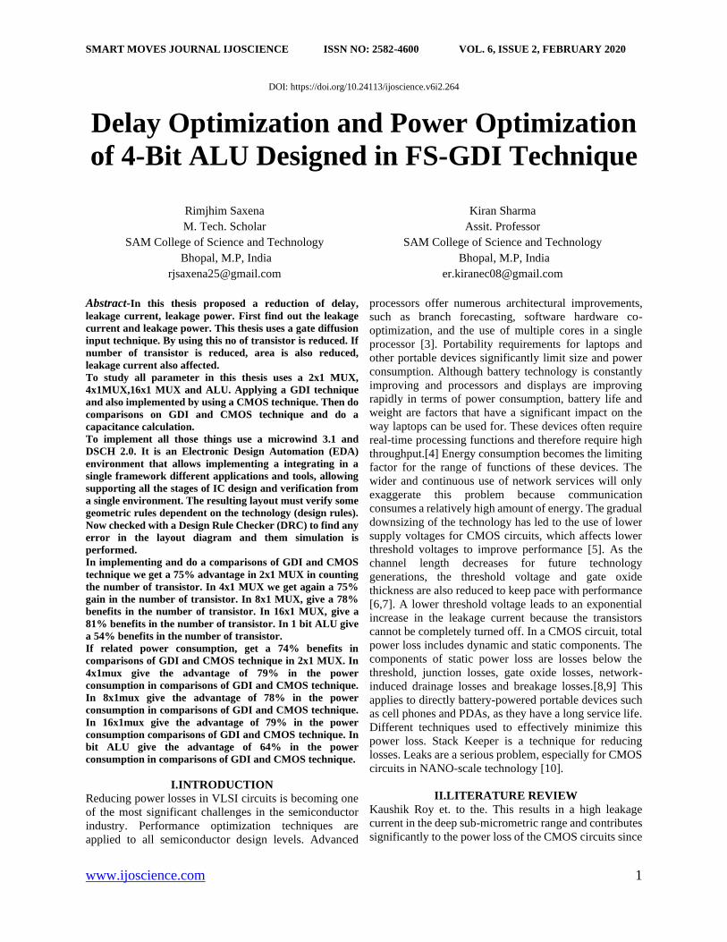
Here we used a circuit diagram to discuss another type of
Figure 1: GDI basic cell
Table -1Some logic functions that can be implemented
with a single GDI cell
N
P G D
′0′
B A 𝐴′𝐵
B
′1′ A 𝐴′ + 𝐵
′1′
B A A+B
B
′0′ A AB
C
B A 𝐴′𝐵 + 𝐴𝐶
′0′
′1′ A 𝐴′
Table 1 shows how a simple change of the input
configuration of the simple GDI cell corresponds to very
different Boolean functions. Most of these functions are
complex (6-12 transistors) in CMOS, as well as in
standard PTL implementations, but very simple (only 2
transistors per function) in GDI design method. This
SMART MOVES JOURNAL IJOSCIENCE ISSN NO: 2582-4600 VOL. 6, ISSUE 2, FEBRUARY 2020
www.ijoscience.com 3
technique also allows reducing power consumption,
propagation delay, and area of digital circuits while
maintaining low complexity of logic design
2) Advantage of GDI Technique
GDI has following benefits over other power reduction
techniques
1. It requires least number of transistors to implement
a MUX.
2. Output swing is rail to rail which has lowered
output swing.
3. It has least static power dissipation as compared to
CMOS.
4. Reduced dynamic component of power
consumption as source of PMOS is not tied to VDD
permanently.
5. Leakage power reduced.
6. Leakage capacitance also reduced
3) Limitations of GDI Technique
GDI MUX has only one limitation that it requires
additional circuitry to restore its full swing.
4) BSIM - Berkeley Short-Channel IGFET Model
The newly developed LEVEL 4 model (Berkeley or
BSIM short channel IGFET model) is analytically simple
and is based on a limited number of parameters that are
normally extracted from experimental data. Its precision
and efficiency make it one of the most popular MOSFET
models today, especially in the microelectronics sector.
Model features include:
1. Continuous and differentiable I-V characteristics
below the threshold, linear and saturation intervals for
good convergence
2. Sensitivity of parameters such as Vt to the length and
width of the transistor
3. Detailed model of the threshold voltage which
includes the body effect and the lowering of the barrier
induced by the discharge
4. Saturation speed, reduced mobility and other short
channel effects
5. Models with multiple door capability
6. Models of diffusion capacity and resistance
7. Network loss models (in BSIM 4)
5) Design Rule
Cadence is an EDA (Electronic Design Automation)
environment that allows you to integrate different
applications and tools into a single framework and
supports all phases of design and verification of integrated
circuits in a single environment. These tools are very
generic and support various production technologies.
When a particular technology is selected, numerous
configuration and technology-related files are used to
customize the Cadence environment. This set of files is
commonly known as a design kit. First, a schematic view
of the circuit is created with the Cadence Composer
circuit diagram editor.
6) LSW
The Layer Selection Window (LSW) lets the user select
different layers of the mask layout. Virtuoso will always
use the layer currently selected in the LSW for editing.
The LSW can also be used to restrict the type of layers
that are visible or selectable. To select a layer, simply
click on the desired layer within the LSW.
Table 2 Minimum width and Minimum spacing Layer Type of rule value
POLY Minimum width
Minimum spacing
2𝜆
2𝜆
ACTIVE Minimum width
Minimum spacing
3𝜆
3𝜆
NSELECT Minimum width
Minimum spacing
3𝜆
3𝜆
PSELECT Minimum width
Minimum spacing
3𝜆
3𝜆
METAL1 Minimum width
Minimum spacing
3𝜆
3𝜆
Table 3 Mosfet Layout Rules Rule Meaning Value
POLY overlap Minimum extension over
ACTIVE
2𝜆
POLY -ACTIVE Minimum spacing 1𝜆
MOSFET width Minimum N+/P+ MOSFET W 3𝜆
ACTIVE CONTACT Exact size
Minimum space to ACTIVE
edge
2𝜆 X 2𝜆
2𝜆
POLY CONTACT Exact size
Minimum space to POLY edge
2𝜆 X 2𝜆
2𝜆
IV. RESULTS
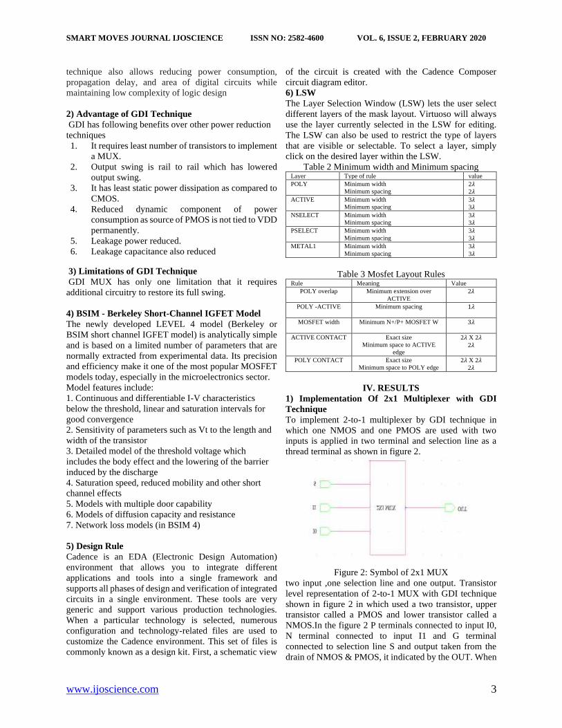
1) Implementation Of 2x1 Multiplexer with GDI
Technique
To implement 2-to-1 multiplexer by GDI technique in
which one NMOS and one PMOS are used with two
inputs is applied in two terminal and selection line as a
thread terminal as shown in figure 2.
Figure 2: Symbol of 2x1 MUX
two input ,one selection line and one output. Transistor
level representation of 2-to-1 MUX with GDI technique
shown in figure 2 in which used a two transistor, upper
transistor called a PMOS and lower transistor called a
NMOS.In the figure 2 P terminals connected to input I0,
N terminal connected to input I1 and G terminal
connected to selection line S and output taken from the
drain of NMOS & PMOS, it indicated by the OUT. When
SMART MOVES JOURNAL IJOSCIENCE ISSN NO: 2582-4600 VOL. 6, ISSUE 2, FEBRUARY 2020
www.ijoscience.com 4
the selection line S is low, input I0 selected. When the
selection line S is high, input I1 selected. In 2x1
multiplexer, selected inputs depend on the selection line,
in other word you can say that selection line controlling
the whole circuit then gives the output.
Figure 3: Transistor level representation of 2-to-1 MUX
with GDI technique
2) Implementation of 4-To-1 Multiplexer with GDI
Technique
In figure 4 shows the transistor level representation of
the 4-to-1 multiplexer with GDI technique in which 4
inputs I0, I1, I2, I3 and two selection lines S0 and S1.
Figure 4: Transistor level representation of 4-to-1 MUX
with GDI technique
3) Implementation of 8×1 Multiplexer With GDI
Technique
Figure 5 shows Transistor level representation of 8-to-1
MUX with GDI technique
Figure 5: Transistor level representation of 8-to-1 MUX
with GDI technique
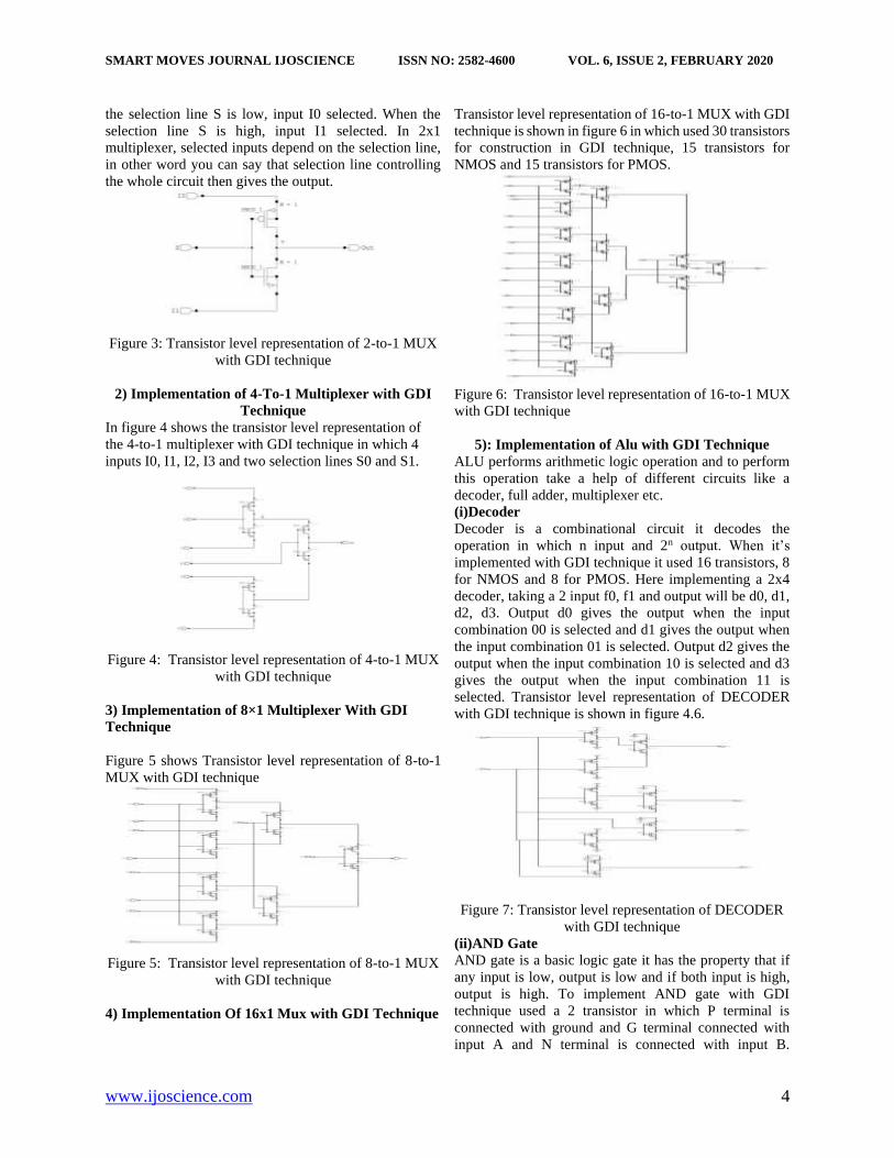
4) Implementation Of 16x1 Mux with GDI Technique
Transistor level representation of 16-to-1 MUX with GDI
technique is shown in figure 6 in which used 30 transistors
for construction in GDI technique, 15 transistors for
NMOS and 15 transistors for PMOS.
Figure 6: Transistor level representation of 16-to-1 MUX
with GDI technique
5): Implementation of Alu with GDI Technique
ALU performs arithmetic logic operation and to perform
this operation take a help of different circuits like a
decoder, full adder, multiplexer etc.
(i)Decoder
Decoder is a combinational circuit it decodes the
operation in which n input and 2n output. When it’s
implemented with GDI technique it used 16 transistors, 8
for NMOS and 8 for PMOS. Here implementing a 2x4
decoder, taking a 2 input f0, f1 and output will be d0, d1,
d2, d3. Output d0 gives the output when the input
combination 00 is selected and d1 gives the output when
the input combination 01 is selected. Output d2 gives the
output when the input combination 10 is selected and d3
gives the output when the input combination 11 is
selected. Transistor level representation of DECODER
with GDI technique is shown in figure 4.6.
Figure 7: Transistor level representation of DECODER
with GDI technique
(ii)AND Gate
AND gate is a basic logic gate it has the property that if
any input is low, output is low and if both input is high,
output is high. To implement AND gate with GDI
technique used a 2 transistor in which P terminal is
connected with ground and G terminal connected with
input A and N terminal is connected with input B.

SMART MOVES JOURNAL IJOSCIENCE ISSN NO: 2582-4600 VOL. 6, ISSUE 2, FEBRUARY 2020
www.ijoscience.com 5
Transistor level representation of AND gate with GDI
technique is shown in figure 4.7.
Figure 8: Transistor level representation of AND gate
with GDI technique
(iii)OR Gate
OR gate is a basic logic gate it has the property that if any
input is high, output is high and if both input is low, output
is low. To implement OR gate with GDI technique used a
2 transistor in which P terminal is connected with input B
and G terminal connected with input A and N terminal is
connected with supply. Transistor level representation of
OR gate with GDI technique is shown in figure 4.8.
Figure 9: Transistor level representation of OR gate with
GDI technique
(iv)NOT GATE
Transistor level representation of NOT gate with GDI
technique is shown in figure 4.9 in which P terminal is
connected with supply and G terminal is connected with
the input A and N terminal is connected with ground and
output is connected with drain of the transistor. To
implement NOT gate with the GDI technique used a two
transistor.
Figure 10: Transistor level representation of NOT gate
with GDI technique
(v)XOR Gate
In the XOR gate when different input occurs like a ‘0’ and
‘1’, output will get high otherwise output is low. Figure
4.10 is shows transistor level representation of XOR gate
with GDI technique in which used a 6 transistor, 3 for
NMOS and 3 for PMOS transistor.
Figure 11: Transistor level representation of XOR gate
with GDI technique
(vi) FULL Adder
Full adder is a combinational circuits it performs the
addition operation. Figure 12 shows a Transistor level
representation of Full adder with GDI technique in which
used an 18 transistor, 9 for NMOS and 9 for PMOS
transistor.
Figure 12: Transistor level representation of Full adder
with GDI technique
(vi) 1-BIT ALU
Figure 4.12 shows a Transistor level representation of 1-
BIT ALU with GDI technique in which used a 54
transistor to implemented, 27 for NMOS and 27 for
PMOS transistor.
Figure 13: Transistor level representation of 1-BIT ALU
with GDI technique

SMART MOVES JOURNAL IJOSCIENCE ISSN NO: 2582-4600 VOL. 6, ISSUE 2, FEBRUARY 2020
www.ijoscience.com 6
6) Layout of 2 -To-1 Multiplexer with GDI Technique
In Figure 14 shows the layout representation of 2 -to-
1MUX with GDI technique in which NMOS makes with
n+ diffusion layer and PMOS makes with p+ diffusion
layer and gate makes with poly silicon and
interconnection shows with metal layers and their contact.
Figure 14: Layout representation of 2 -to-1MUX with
GDI technique
Figure 15: Voltage vs. time simulation of 2 -to-1 MUX
with GDI technique
Figure 15 shows a Voltage vs. time simulation of 2 -to-1
MUX with GDI technique in which indicate a operation
performed by 2x1 multiplexer. Figure 16 : Voltage vs.
current simulation in 2 -to-1 MUX with GDI technique
in which shows a different fluctuation spike related to
current.
Figure 16: Voltage vs. current simulation in 2 -to-1
MUX with GDI technique
7) Layout of 4 -To-1 Multiplexer with GDI Technique
Figure 17: Layout representation of 4 -to-1 MUX with
GDI technique
Figure 17 shows layout representation of 4 -to-1 MUX
with GDI technique in which indicate the operation and
their Voltage vs. time simulation of 4 -to-1 MUX with
GDI technique is shows in figure 18. Figure 19 shows a
Voltage vs. current simulation in 4 -to-1 MUX with GDI
technique.
Figure 18: Voltage vs. time simulation of 4 -to-1 MUX
with GDI technique
Figure 19: Voltage vs. current simulation in 4 -to-1
MUX with GDI technique
8) Layout of 8 -To-1 Multiplexer with GDI Technique
Figure 20 shows a layout representation of 8 -to-1 MUX
with GDI technique
Figure 20: Layout representation of 8 -to-1 MUX with
GDI technique
SMART MOVES JOURNAL IJOSCIENCE ISSN NO: 2582-4600 VOL. 6, ISSUE 2, FEBRUARY 2020
www.ijoscience.com 7
Figure 21: Voltage vs. time simulation of 8 -to-1 MUX
with GDI technique
Figure 21 shows a Voltage vs. time simulation of 8 -to-1
MUX with GDI technique in which output indicate the
operation of 8x1 multiplexer. Figure 22 shows a Voltage
vs. current simulation in 8 -to-1 MUX with GDI
technique in which shows a behavior of current with
reference to voltage.
Figure 22: Voltage vs. current simulation in 8 -to-1
MUX with GDI technique
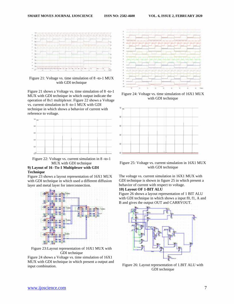
9) Layout of 16 -To-1 Multiplexer with GDI
Technique
Figure 23 shows a layout representation of 16X1 MUX
with GDI technique in which used a different diffusion
layer and metal layer for interconnection.
Figure 23:Layout representation of 16X1 MUX with
GDI technique
Figure 24 shows a Voltage vs. time simulation of 16X1
MUX with GDI technique in which present a output and
input combination.
Figure 24: Voltage vs. time simulation of 16X1 MUX
with GDI technique
Figure 25: Voltage vs. current simulation in 16X1 MUX
with GDI technique
The voltage vs. current simulation in 16X1 MUX with
GDI technique is shown in figure 25 in which present a
behavior of current with respect to voltage.
10) Layout OF 1-BIT ALU
Figure 26 shows a layout representation of 1 BIT ALU
with GDI technique in which shows a input f0, f1, A and
B and gives the output OUT and CARRYOUT.
Figure 26: Layout representation of 1.BIT ALU with
GDI technique
SMART MOVES JOURNAL IJOSCIENCE ISSN NO: 2582-4600 VOL. 6, ISSUE 2, FEBRUARY 2020
www.ijoscience.com 8
Figure 27 shows a Voltage vs. time simulation of 1BIT
ALU with GDI technique in which output shows the
operation specified in ALU.
Figure 27: Voltage vs. time simulation of 1BIT ALU
with GDI technique
Figure 28 shows a Voltage vs. current simulation in 1BIT
ALU with GDI technique in which indicates behavior of
current.
Figure 28: Voltage vs. current simulation in 1BIT ALU
with GDI technique
11) Implementation of 2-To-1 Multiplexer with
CMOS Technique
Figure 29 shows a Transistor level implementation 0f 2-
to-1 MUX with CMOS technique in which present a 8
transistor is used, 4 for PMOS and 4 for NMOS transistor.
Figure 29: Transistor level implementation 0f 2-to-1
MUX with CMOS technique
12) Implementation of 4-To-1 Multiplexer with
CMOS Technique
Figure 30 shows a Transistor level implementation of 4-
to-1 MUX with CMOS technique in which 24 transistor
are used, 12 for PMOS and 12 for NMOS transistor and
Figure 30: Transistor level implementation 0f 4-to-1
MUX with CMOS technique
13) Implementation of 8-To-1 Multiplexer With
CMOS Technique
Figure 31 shows a Transistor level implementation 0f 8-
to-1 MUX with CMOS technique in which used a 64
transistor, 32 transistors for NMOS and 32 transistors for
PMOS.
Figure 31: Transistor level implementation 0f 8-to-1
MUX with CMOS technique
14) Implementation of 16x1 Mux with CMOS
Technique
Figure 32 shows a Transistor level implementation of 16-
to-1 MUX with CMOS technique in which used a 160
transistor, 80 for NMOS and 80 for PMOS transistor.
Figure 32: Transistor level implementation 0f 16-to-1
MUX with CMOS technique
15) Implementation of 1bit Alu With CMOS
Technique
Figure 33 shows a Transistor level implementation of 1
BIT ALU with CMOS technique in which used a 118
transistor, 59 for NMOS and 59 for PMOS.

SMART MOVES JOURNAL IJOSCIENCE ISSN NO: 2582-4600 VOL. 6, ISSUE 2, FEBRUARY 2020
www.ijoscience.com 9
Figure 33: Transistor level implementation of 1 BIT
ALU with CMOS technique
16) Layout of 2-To-1 Multiplexer with CMOS
Technique
Figure 34 shows a layout representation of 2 -to-1 MUX
with CMOS technique. Voltage vs. time simulation of 2 -
to-1 MUX with CMOS technique is shown in figure 4.34.
Figure 34: Layout representation of 2 -to-1 MUX with
CMOS technique
Figure 35: Voltage vs. time simulation of 2 -to-1 MUX
with CMOS technique
Figure 36 shows a Voltage vs. current simulation in 2 -
to-1 MUX with CMOS technique
Figure 36: Voltage vs. current simulation in 2 -to-1
MUX with CMOS technique
17) Layout of 4-To-1 Multiplexer with CMOS
Technique
Figure 37 shows a layout representation of 4 -to-1 MUX
with CMOS technique and Voltage vs. time simulation of
4 -to-1 MUX with CMOS technique shows a Figure 4.37.
Voltage vs. current simulation in 4 -to-1 MUX with
CMOS technique shows a figure 39.
Figure 37: Layout representation of 4 -to-1 MUX with
CMOS technique
Figure 38 : Voltage vs. time simulation of 4 -to-1 MUX
with CMOS technique
Figure 39: Voltage vs. current simulation in 4 -to-1
MUX with CMOS technique
18) Layout of 8-To-1 Multiplexer with CMOS
Technique
Figure 40: Layout representation of 8 -to-1 MUX with
CMOS technique

SMART MOVES JOURNAL IJOSCIENCE ISSN NO: 2582-4600 VOL. 6, ISSUE 2, FEBRUARY 2020
www.ijoscience.com 10
Figure 41: Voltage vs. time simulation of 8 -to-1 MUX
with CMOS technique
Figure 42: Voltage vs. current simulation in 8 -to-1
MUX with CMOS technique
19) Layout of 16x1mux with CMOS Technique
Figure 43 shows a layout representation of 16 -to-1 MUX
with CMOS technique and Voltage vs. time simulation of
16 -to-1 MUX with CMOS technique shown in Figure 44
and Figure 45 shows a Voltage vs. current simulation in
16 -to-1 MUX with CMOS technique.
Figure 43: Layout representation of 16 -to-1 MUX with
CMOS technique
Figure 44: Voltage vs. time simulation of 16 -to-1 MUX
with CMOS technique
Figure 45: Voltage vs. current simulation in 16 -to-1
MUX with CMOS technique
TABLE 4 Comparision Between GDI and CMOS
According To Number of Transistors Device
No. of Transistor in CMOS No. of Transistor in GDI
2X1 MUX 8 2
4X1 MUX 24 6
8X1 MUX 64 14
16X1 MUX 160 30
1-Bit ALU 118 54
TABLE – 5 Simulation Result in Term of Leakage
Current Device
Leakage current in CMOS Leakage current in GDI
2X1 MUX 0.137ma 0.007ma
4X1 MUX 1.43ma 0.212ma
8X1 MUX 2.96ma 0.122ma
16X1 MUX 4.43ma 1.13ma
1-Bit ALU 8.98ma 3.77ma
TABLE – 6 Simulation Result of in Term of Dynamic
Power Consumption Device
Dynamic power
consumption in CMOS
Dynamic power
consumption in GDI
2X1 MUX 9.88µw 2.56µw
4X1 MUX 16.09µw 3.23µw
8X1 MUX 24.16µw 5.134µw
16X1 MUX 74.55µw 15.01µw
1-Bit ALU 112.5µw 40.3µw
TABLE – 7 Simulation Result of in Term Of Delay
Device
Delay in CMOS Delay in GDI
2X1 MUX 7.21 ps 4.34 ps
4X1 MUX 13.89 ps 11.43 ps
8X1 MUX 26.54 ps 21.35 ps
16X1 MUX 50.12 ps 42.76 ps
1-Bit ALU 69.5ps 53.21ps
IV.CONCLUSION
In this thesis proposed a reduction of leakage current,
leakage power and leakage capacitance. First find out the
leakage current and leakage power from the statistical
analysis and then find out the capacitance .in this uses a
gate diffusion input technique. By using this no of
transistor is reduced. If number of transistor is reduced,
area is also reduced, leakage current also affected.
SMART MOVES JOURNAL IJOSCIENCE ISSN NO: 2582-4600 VOL. 6, ISSUE 2, FEBRUARY 2020
www.ijoscience.com 11
To study all parameter in this thesis uses a 2x1 MUX,
4x1MUX,16x1 MUX and ALU. Applying a GDI
technique and also implemented by using a CMOS
technique. Then do comparisons on GDI and CMOS
technique.
Use a virtuoso cadence to implement all these things.
Cadence is an electronic design automation (EDA)
environment that allows the implementation of various
applications and tools in a single framework and supports
all the design and verification phases of integrated circuits
in a single environment.
In the comparisons from the CMOS technique and GDI
technique we get a number of transistors to implement a
2x1 MUX is 8 for CMOS and 2 for GDI technique. In 4x1
MUX, a number of transistors are 24 for CMOS and 6 for
GDI technique. In 8x1 MUX, a number of transistors are
64 for CMOS and 14 for GDI technique. In 16x1 MUX, a
number of transistors are 160 for CMOS and 30 for GDI
technique. In 1 bit ALU, a number of transistors are 118
for CMOS and 54 for GDI technique.
In the comparisons from the CMOS technique and GDI
technique, leakage current in 2x1MUX is 0.137ma in
CMOS and 0,007ma in GDI technique. In the 4x1MUX,
get the leakage current is 1.43ma in CMOS and 0.212ma
in GDI technique. In the 8x1MUX, get the leakage current
is 2.96ma in CMOS and 0122ma in GDI technique. In the
16x1MUX, get the leakage current is 4.43ma in CMOS
and 1.13ma in GDI technique. In the 1 bit ALU, get the
leakage current is 8.98ma in CMOS and 3.77ma in GDI
technique.
In this all implementation power dissipation is also
reduced. In 2x1 MUX power dissipation is 9.88µw in
CMOS technique and 2.56 µw in GDI technique. In 4x1
MUX power dissipation is 16.09µw in CMOS technique
and 3.23 µw in GDI technique. In 8x1 MUX power
dissipation is 24.16µw in CMOS technique and 5.134 µw
in GDI technique. In 16x1 MUX power dissipation is
74.55µw in CMOS technique and 15.01 µw in GDI
technique. In 1 bit ALU power dissipation is 112.5µw in
CMOS technique and 40.3 µw in GDI technique.
In implementing and do a comparisons of GDI and CMOS
technique we get a 75% advantage in 2x1 MUX in
counting the number of transistor. In 4x1 MUX we get
again a 75% gain in the number of transistor. In 8x1
MUX, give a 78% benefits in the number of transistor. In
16x1 MUX, give a 81% benefits in the number of
transistor. In 1 bit ALU give a 54% benefits in the number
of transistor.
In reference of leakage current or leakage power, get a
94% benefits in comparisons of GDI and CMOS
technique in 2x1 MUX. In 4x1MUX give the advantage
of 85% in the leakage current in comparisons of GDI and
CMOS technique. In 8x1MUX give the advantage of 95%
in the leakage current in comparisons of GDI and CMOS
technique. In 16x1MUX give the advantage of 74% in the
leakage current comparisons of GDI and CMOS
technique. In bit ALU give the advantage of 58% in the
leakage current in comparisons of GDI and CMOS
technique.
If related power consumption, get a 74% benefits in
comparisons of GDI and CMOS technique in 2x1 MUX.
In 4x1MUX give the advantage of 79% in the power
consumption in comparisons of GDI and CMOS
technique. In 8x1MUX give the advantage of 78% in the
power consumption in comparisons of GDI and CMOS
technique. In 16x1MUX give the advantage of 79% in the
power consumption comparisons of GDI and CMOS
technique. In bit ALU give the advantage of 64% in the
power consumption in comparisons of GDI and CMOS
technique.
V.FUTURE WORK
The power dissipation of electronic products has become
a major problem in connection with the huge growth of
laptops and wireless communications in recent years.
Since the power consumption is directly proportional to
the square of the supply voltage, the MOS transistor has
been scaled down to maintain performance with the
supply voltage reduced. The threshold voltage of the
transistor is also reduced to avoid a short channel effect,
which causes a significant increase in the leakage currents
when the transistor evolves into nanometric dimensions.
Backup power represents a significant part of the total
energy consumption of integrated circuits.
REFERENCES [1] Vijaya Shekhawat, Tripti Sharma and Krishna Gopal Sharma,” 2-
Bit Magnitude Comparator using GDI Technique”, IEEE
International Conference on Recent Advances and Innovations in
Engineering (ICRAIE-2014), May 09-11, 2014, Jaipur, India.
[2] Krishnendu Dhar, Aanan Chatterjee, Sayan Chatterjee,” Design of
Energy Efficient High Speed Low Power Full Subtractor Using
GDI Technique”, IEEE, 2014.
[3] Gholamreza Shomalnasab and Lihong Zhang,” New Analytic
Model of Coupling and Substrate Capacitance in Nanometer
Technologies”, IEEE Transactions on Very Large Scale
Integration (VLSI) Systems, IEEE 2014.
[4] Mohammad Shueb Romi, Naushad Alam, and M. Yusuf Yasin,”
An Analytical Delay Model for CMOS Inverter-Transmission
Gate Structure”, IEEE 2014.
[5] Krishnendu Dhar,” Design of a High Speed, Low Power
Synchronously Clocked NOR-based JK Flip-Flop using Modified
GDI Technique in 45nm Technology”, IEEE 2014.
[6] E.J. Priyanka, S. Vanitha, P.C.Rupa,” Design Of GDI Based 4-Bit
Multiplier Using Low Power Adder Cells”, National Conference
On VLSI And Embedded Systems 2013.
[7] Kaushik Roy, Fellow, IEEE, Saibal Mukhopadhyay, Student
Member, IEEE, And Hamid Mahmoodi-Meimand,” Leakage
Current Mechanisms And Leakage Reduction Techniques In
Deep-Submicrometer CMOS Circuits”, IEEE, Vol. 91, No. 2,
February 2013.
[8] Afshin Abdollahi, Farzan Fallah, Massoud Pedram,” Leakage
Current Reduction In Sequential Circuits By Modifying The Scan
Chains”, International Symposium On Quality Electronic Design
(ISQED’03) 2003 IEEE.

SMART MOVES JOURNAL IJOSCIENCE ISSN NO: 2582-4600 VOL. 6, ISSUE 2, FEBRUARY 2020
www.ijoscience.com 12
[9] Afshin Abdollahi, Farzan Fallah, And Massoud Pedram,” Leakage
Current Reduction In CMOS VLSI Circuits By Input Vector
Control”, IEEE Transactions On Very Large Scale Integration
(VLSI) Systems, Vol. 12, No. 2, February 2004.
[10] Dongwoo Lee, Student Member, IEEE, David Blaauw, Member,
IEEE, And Dennis Sylvester, Member, IEEE,” Gate Oxide
Leakage Current Analysis And Reduction For VLSI Circuits”,
IEEE Transactions On Very Large Scale Integration (VLSI)
Systems, Vol. 12, No. 2, February 2004.