16-Bit Sigma-Delta ADCs - All Products
32
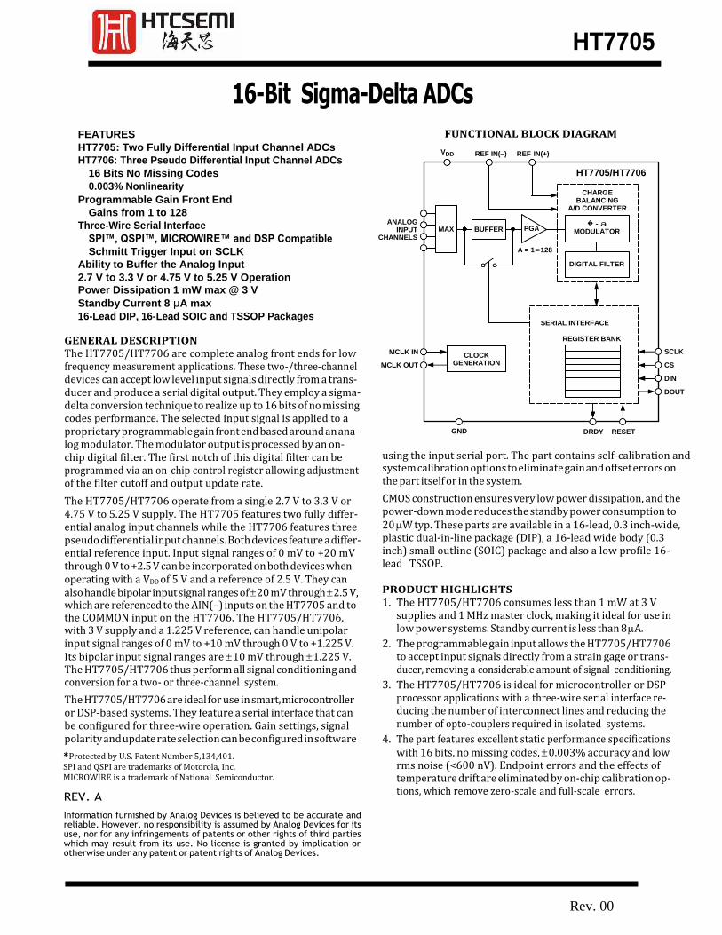
FEATURES FUNCTIONAL BLOCK DIAGRAM HT7705: Two Fully Differential Input Channel ADCs HT7706: Three Pseudo Differential Input Channel ADCs 16 Bits No Missing Codes 0.003% Nonlinearity Programmable Gain Front End Gains from 1 to 128 Three-Wire Serial Interface SPI™, QSPI™, MICROWIRE™ and DSP Compatible Schmitt Trigger Input on SCLK Ability to Buffer the Analog Input 2.7 V to 3.3 V or 4.75 V to 5.25 V Operation Power Dissipation 1 mW max @ 3 V Standby Current 8 μ A max 16-Lead DIP, 16-Lead SOIC and TSSOP Packages GENERAL DESCRIPTION The HT7705/HT7706 are complete analog front ends for low frequency measurement applications. These two-/three-channel devices can accept low level input signals directly from a trans- ducer and produce a serial digital output. They employ a sigma- delta conversion technique to realize up to 16 bits of no missing codes performance. The selected input signal is applied to a proprietary programmable gain front end based around an ana- log modulator. The modulator output is processed by an on- ANALOG INPUT CHANNELS MCLK IN MCLK OUT V DD REF IN(–) REF IN(+) GND DRDY RESET SCLK CS DIN DOUT chip digital filter. The first notch of this digital filter can be programmed via an on-chip control register allowing adjustment of the filter cutoff and output update rate. The HT7705/HT7706 operate from a single 2.7 V to 3.3 V or 4.75 V to 5.25 V supply. The HT7705 features two fully differ- ential analog input channels while the HT7706 features three pseudo differential input channels. Both devices feature a differ- ential reference input. Input signal ranges of 0 mV to +20 mV through 0 V to +2.5 V can be incorporated on both devices when operating with a VDD of 5 V and a reference of 2.5 V. They can also handle bipolar input signal ranges of 20 mV through 2.5 V, which are referenced to the AIN(–) inputs on the HT7705 and to the COMMON input on the HT7706. The HT7705/HT7706, with 3 V supply and a 1.225 V reference, can handle unipolar input signal ranges of 0 mV to +10 mV through 0 V to +1.225 V. Its bipolar input signal ranges are 10 mV through 1.225 V. The HT7705/HT7706 thus perform all signal conditioning and conversion for a two- or three-channel system. The HT7705/HT7706 are ideal for use in smart, microcontroller or DSP-based systems. They feature a serial interface that can be configured for three-wire operation. Gain settings, signal polarity and update rate selection can be configured in software *Protected by U.S. Patent Number 5,134,401. SPI and QSPI are trademarks of Motorola, Inc. MICROWIRE is a trademark of National Semiconductor. REV. A Information furnished by Analog Devices is believed to be accurate and reliable. However, no responsibility is assumed by Analog Devices for its use, nor for any infringements of patents or other rights of third parties which may result from its use. No license is granted by implication or otherwise under any patent or patent rights of Analog Devices. using the input serial port. The part contains self-calibration and system calibration options to eliminate gain and offset errors on the part itself or in the system. CMOS construction ensures very low power dissipation, and the power-down mode reduces the standby power consumption to 20 W typ. These parts are available in a 16-lead, 0.3 inch-wide, plastic dual-in-line package (DIP), a 16-lead wide body (0.3 inch) small outline (SOIC) package and also a low profile 16- lead TSSOP. PRODUCT HIGHLIGHTS 1. The HT7705/HT7706 consumes less than 1 mW at 3 V supplies and 1 MHz master clock, making it ideal for use in low power systems. Standby current is less than 8 A. 2. The programmable gain input allows the HT7705/HT7706 to accept input signals directly from a strain gage or trans- ducer, removing a considerable amount of signal conditioning. 3. The HT7705/HT7706 is ideal for microcontroller or DSP processor applications with a three-wire serial interface re- ducing the number of interconnect lines and reducing the number of opto-couplers required in isolated systems. 4. The part features excellent static performance specifications with 16 bits, no missing codes, 0.003% accuracy and low rms noise (<600 nV). Endpoint errors and the effects of temperature drift are eliminated by on-chip calibration op- tions, which remove zero-scale and full-scale errors. CHARGE BALANCING A/D CONVERTER MAX BUFFER � - a MODULATOR DIGITAL FILTER SERIAL INTERFACE REGISTER BANK HT7705/HT7706 PGA A = 1=128 CLOCK GENERATION HT7705 Rev. 00 16-Bit Sigma-Delta ADCs
-
Upload
khangminh22 -
Category
Documents
-
view
1 -
download
0
Transcript of 16-Bit Sigma-Delta ADCs - All Products
FEATURES
FUNCTIONAL BLOCK DIAGRAM
HT7705: Two Fully Differential Input Channel ADCs
HT7706: Three Pseudo Differential Input Channel ADCs
16 Bits No Missing Codes
0.003% Nonlinearity
Programmable Gain Front End
Gains from 1 to 128
Three-Wire Serial Interface
SPI™, QSPI™, MICROWIRE™ and DSP Compatible
Schmitt Trigger Input on SCLK
Ability to Buffer the Analog Input
2.7 V to 3.3 V or 4.75 V to 5.25 V Operation
Power Dissipation 1 mW max @ 3 V
Standby Current 8 µA max
16-Lead DIP, 16-Lead SOIC and TSSOP Packages
GENERAL DESCRIPTION The HT7705/HT7706 are complete analog front ends for low frequency measurement applications. These two-/three-channel devices can accept low level input signals directly from a trans- ducer and produce a serial digital output. They employ a sigma- delta conversion technique to realize up to 16 bits of no missing codes performance. The selected input signal is applied to a proprietary programmable gain front end based around an ana- log modulator. The modulator output is processed by an on-
ANALOG
INPUT CHANNELS
MCLK IN
MCLK OUT
VDD REF IN(–) REF IN(+)
GND DRDY RESET
SCLK
CS
DIN
DOUT
chip digital filter. The first notch of this digital filter can be programmed via an on-chip control register allowing adjustment of the filter cutoff and output update rate.
The HT7705/HT7706 operate from a single 2.7 V to 3.3 V or 4.75 V to 5.25 V supply. The HT7705 features two fully differ- ential analog input channels while the HT7706 features three pseudo differential input channels. Both devices feature a differ- ential reference input. Input signal ranges of 0 mV to +20 mV through 0 V to +2.5 V can be incorporated on both devices when operating with a VDD of 5 V and a reference of 2.5 V. They can also handle bipolar input signal ranges of 20 mV through 2.5 V, which are referenced to the AIN(–) inputs on the HT7705 and to the COMMON input on the HT7706. The HT7705/HT7706, with 3 V supply and a 1.225 V reference, can handle unipolar input signal ranges of 0 mV to +10 mV through 0 V to +1.225 V. Its bipolar input signal ranges are 10 mV through 1.225 V. The HT7705/HT7706 thus perform all signal conditioning and conversion for a two- or three-channel system.
The HT7705/HT7706 are ideal for use in smart, microcontroller or DSP-based systems. They feature a serial interface that can be configured for three-wire operation. Gain settings, signal polarity and update rate selection can be configured in software
*Protected by U.S. Patent Number 5,134,401. SPI and QSPI are trademarks of Motorola, Inc. MICROWIRE is a trademark of National Semiconductor.
REV. A
Information furnished by Analog Devices is believed to be accurate and reliable. However, no responsibility is assumed by Analog Devices for its use, nor for any infringements of patents or other rights of third parties which may result from its use. No license is granted by implication or otherwise under any patent or patent rights of Analog Devices.
using the input serial port. The part contains self-calibration and system calibration options to eliminate gain and offset errors on the part itself or in the system.
CMOS construction ensures very low power dissipation, and the power-down mode reduces the standby power consumption to 20 W typ. These parts are available in a 16-lead, 0.3 inch-wide, plastic dual-in-line package (DIP), a 16-lead wide body (0.3 inch) small outline (SOIC) package and also a low profile 16- lead TSSOP.
PRODUCT HIGHLIGHTS 1. The HT7705/HT7706 consumes less than 1 mW at 3 V
supplies and 1 MHz master clock, making it ideal for use in low power systems. Standby current is less than 8 A.
2. The programmable gain input allows the HT7705/HT7706 to accept input signals directly from a strain gage or trans- ducer, removing a considerable amount of signal conditioning.
3. The HT7705/HT7706 is ideal for microcontroller or DSP processor applications with a three-wire serial interface re- ducing the number of interconnect lines and reducing the number of opto-couplers required in isolated systems.
4. The part features excellent static performance specifications with 16 bits, no missing codes, 0.003% accuracy and low rms noise (<600 nV). Endpoint errors and the effects of temperature drift are eliminated by on-chip calibration op- tions, which remove zero-scale and full-scale errors.
CHARGE BALANCING
A/D CONVERTER
MAX
BUFFER � - a
MODULATOR
DIGITAL FILTER
SERIAL INTERFACE
REGISTER BANK
HT7705/HT7706
PGA
A = 1=128
CLOCK GENERATION
HT7705
Rev. 00
16-Bit Sigma-Delta ADCs
Parameter B Version1 Units Conditions/Comments
STATIC PERFORMANCE No Missing Codes 16 Bits min Guaranteed by Design. Filter Notch < 60 Hz Output Noise See Tables I and III Depends on Filter Cutoffs and Selected Gain Integral Nonlinearity2
0.003 % of FSR max Filter Notch < 60 Hz. Typically 0.0003% Unipolar Offset Error Unipolar Offset Drift4
See Note 3 0.5 V/C typ
Bipolar Zero Error Bipolar Zero Drift4
Positive Full-Scale Error5
Full-Scale Drift4, 6
Gain Error7
Gain Drift4, 8
Bipolar Negative Full-Scale Error2
Bipolar Negative Full-Scale Drift4
See Note 3 0.5 0.1 See Note 3 0.5 See Note 3 0.5 0.003 1 0.6
V/C typ V/C typ
V/C typ
ppm of FSR/C typ % of FSR typ V/C typ V/C typ
For Gains 1, 2 and 4 For Gains 8, 16, 32, 64 and 128
Typically 0.001% For Gains of 1 to 4 For Gains of 8 to 128
ANALOG INPUTS/REFERENCE INPUTS Input Common-Mode Rejection (CMR)2
VDD = 5 V Gain = 1 Gain = 2 Gain = 4 Gain = 8v128
VDD = 3 V Gain = 1 Gain = 2 Gain = 4 Gain = 8v128
Normal-Mode 50 Hz Rejection2
Normal-Mode 60 Hz Rejection2
Common-Mode 50 Hz Rejection2
Common-Mode 60 Hz Rejection2
Absolute/Common-Mode REF IN Voltage2
Absolute/Common-Mode AIN Voltage2, 9
Absolute/Common-Mode AIN Voltage2, 9
AIN DC Input Current2
AIN Sampling Capacitance2
AIN Differential Voltage Range10
AIN Input Sampling Rate, fS
Reference Input Range REF IN(+) – REF IN(–) Voltage
REF IN(+) – REF IN(–) Voltage
REF IN Input Sampling Rate, fS
Specifications for AIN and REF IN Unless Noted
96
dB typ
105 dB typ 110 dB typ 130 dB typ
105 dB typ 110 dB typ 120 dB typ 130 98
dB typ dB typ For Filter Notches of 25 Hz, 50 Hz, 0.02 fNOTCH
98 dB typ For Filter Notches of 20 Hz, 60 Hz, 0.02 fNOTCH
150 dB typ For Filter Notches of 25 Hz, 50 Hz, 0.02 fNOTCH
150 GND to VDD
GND – 30 mV
dB typ V min to V max V min
For Filter Notches of 20 Hz, 60 Hz, 0.02 fNOTCH
BUF Bit of Setup Register = 0 VDD + 30 mV GND + 50 mV
V max V min
BUF Bit of Setup Register = 1 VDD – 1.5 V 1
V max nA max
10
0 to +VREF/GAIN11
pF max nom
Unipolar Input Range (B/U Bit of Setup Register = 1)
VREF/GAIN nom Bipolar Input Range (B/U Bit of Setup Register = 0) GAIN fCLKIN/64 fCLKIN/8
For Gains of 1 to 4 For Gains of 8 to 128
1/1.75 V min/max VDD = 2.7 V to 3.3 V. VREF = 1.225 1% for Specified
Performance 1/3.5 V min/max VDD = 4.75 V to 5.25 V. VREF = 2.5 1% for Specified
Performance fCLKIN/64
LOGIC INPUTS Input Current
All Inputs Except MCLK IN MCLK
All Inputs Except SCLK and MCLK IN VINL, Input Low Voltage
VINH, Input High Voltage SCLK Only (Schmitt Triggered Input)
VT+
VT–
VT+ – VT–
SCLK Only (Schmitt Triggered Input) VT+
VT–
VT+ – VT–
MCLK IN Only VINL, Input Low Voltage VINH, Input High Voltage
MCLK IN Only VINL, Input Low Voltage VINH, Input High Voltage
1
A max
Typically 20 nA 10 A max Typically 2 A
0.8 0.4 2.0
V max V max V min
VDD = 5 V VDD = 3 V VDD = 3 V and 5 V
1.4/3
V min/V max VDD = 5 V NOMINAL
0.8/1.4 V min/V max 0.4/0.8 V min/V max
1/2.5
V min/V max VDD = 3 V NOMINAL
0.4/1.1 V min/V max 0.375/0.8 V min/V max
0.8
V max
VDD = 5 V NOMINAL
3.5 V min
0.4 V max
HT7705
Rev. 00
Parameter B Version1 Units Conditions/Comments
LOGIC OUTPUTS (Including MCLK OUT) VOL, Output Low Voltage VOL, Output Low Voltage VOH, Output High Voltage VOH, Output High Voltage Floating State Leakage Current Floating State Output Capacitance13
0.4 0.4 4 VDD–0.6 10 9
V max V max V min V min A max pF typ
ISINK = 800 A Except for MCLK OUT.12 VDD = 5 V. ISINK = 100 A Except for MCLK OUT.12 VDD = 3 V. ISOURCE = 200 A Except for MCLK OUT.12 VDD = 5 V. ISOURCE = 100 A Except for MCLK OUT.12 VDD = 3 V.
Data Output Coding Binary Unipolar Mode
Offset Binary Bipolar Mode
SYSTEM CALIBRATION Positive Full-Scale Calibration Limit14
Negative Full-Scale Calibration Limit14
Offset Calibration Limit14
Input Span15
(1.05 VREF)/GAIN –(1.05 VREF)/GAIN –(1.05 VREF)/GAIN (0.8 VREF)/GAIN
V max V max V max V min
GAIN Is the Selected PGA Gain (1 to 128) GAIN Is the Selected PGA Gain (1 to 128) GAIN Is the Selected PGA Gain (1 to 128) GAIN Is the Selected PGA Gain (1 to 128)
(2.1 VREF)/GAIN V max GAIN Is the Selected PGA Gain (1 to 128)
POWER REQUIREMENTS VDD Voltage
Power Supply Currents16
VDD Voltage Power Supply Currents16
Standby (Power-Down) Current17
Power Supply Rejection18
+2.7 to +3.3
V min to V max
For Specified Performance
Digital I/Ps = 0 V or VDD. External MCLK IN and
CLK DIS = 1 0.32 0.6 0.4 0.6 0.7 1.1 +4.75 to +5.25
mA max mA max mA max mA max mA max mA max V min to V max
BUF Bit = 0. fCLKIN = 1 MHz. Gains of 1 to 128 BUF Bit = 1. fCLKIN = 1 MHz. Gains of 1 to 128 BUF Bit = 0. fCLKIN = 2.4576 MHz. Gains of 1 to 4 BUF Bit = 0. fCLKIN = 2.4576 MHz. Gains of 8 to 128 BUF Bit = 1. fCLKIN = 2.4576 MHz. Gains of 1 to 4 BUF Bit = 1. fCLKIN = 2.4576 MHz. Gains of 8 to 128 For Specified Performance
Digital I/Ps = 0 V or VDD. External MCLK IN and
CLK DIS = 1. 0.45 0.7 0.6 0.85 0.9 1.3 16 8
mA max mA max mA max mA max mA max mA max A max A max
BUF Bit = 0. fCLKIN = 1 MHz. Gains of 1 to 128 BUF Bit = 1. fCLKIN = 1 MHz. Gains of 1 to 128 BUF Bit = 0. fCLKIN = 2.4576 MHz. Gains of 1 to 4 BUF Bit = 0. fCLKIN = 2.4576 MHz. Gains of 8 to 128 BUF Bit = 1. fCLKIN = 2.4576 MHz. Gains of 1 to 4 BUF Bit = 1. fCLKIN = 2.4576 MHz. Gains of 8 to 128 External MCLK IN = 0 V or VDD. VDD = 5 V. See Figure 9 External MCLK IN = 0 V or VDD. VDD = 3 V
See Note 19 dB typ NOTES
1Temperature range as follows: B Version, –40C to +85C. 2These numbers are established from characterization or design at initial product release. 3A calibration is effectively a conversion so these errors will be of the order of the conversion noise shown in Tables I and III. This applies after calibration at the
temperature of interest. 4Recalibration at any temperature will remove these drift errors. 5Positive Full-Scale Error includes Zero-Scale Errors (Unipolar Offset Error or Bipolar Zero Error) and applies to both unipolar and bipolar input ranges. 6Full-Scale Drift includes Zero-Scale Drift (Unipolar Offset Drift or Bipolar Zero Drift) and applies to both unipolar and bipolar input ranges. 7Gain Error does not include Zero-Scale Errors. It is calculated as Full-Scale Error–Unipolar Offset Error for unipolar ranges and Full-Scale Error–Bipolar Zero Error for
bipolar ranges. 8Gain Error Drift does not include Unipolar Offset Drift/Bipolar Zero Drift. It is effectively the drift of the part if zero scale calibrations only were performed. 9This common-mode voltage range is allowed provided that the input voltage on analog inputs does not go more positive than VDD + 30 mV or go more negative than GND – 30 mV. Parts are functional with voltages down to GND – 200 mV, but with increased leakage at high temperature.
10The analog input voltage range on AIN(+) is given here with respect to the voltage on AIN(–) on the HT7705 and is given with respect to the COMMON input on the HT7706. The absolute voltage on the analog inputs should not go more positive than VDD + 30 mV, or go more negative than GND – 30 mV for specified performance, input voltages of GND – 200 mV can be accommodated, but with increased leakage at high temperature.
11VREF = REF IN(+) – REF IN(–). 12These logic output levels apply to the MCLK OUT only when it is loaded with one CMOS load. 13Sample tested at +25C to ensure compliance. 14After calibration, if the analog input exceeds positive full scale, the converter will output all 1s. If the analog input is less than negative full scale, the device will output all 0s. 15These calibration and span limits apply provided the absolute voltage on the analog inputs does not exceed VDD + 30 mV or go more negative than GND – 30 mV. The offset
calibration limit applies to both the unipolar zero point and the bipolar zero point. 16When using a crystal or ceramic resonator across the MCLK pins as the clock source for the device, the VDD current and power dissipation will vary depending on the crystal or
resonator type (see Clocking and Oscillator Circuit section). 17If the external master clock continues to run in standby mode, the standby current increases to 150 A typical at 5 V and 75 A at 3 V. When using a crystal or ceramic
resonator across the MCLK pins as the clock source for the device, the internal oscillator continues to run in standby mode and the power dissipation depends on the crystal or resonator type (see Standby Mode section).
18Measured at dc and applies in the selected passband. PSRR at 50 Hz will exceed 120 dB with filter notches of 25 Hz or 50 Hz. PSRR at 60 Hz will exceed 120 dB with filter notches of 20 Hz or 60 Hz.
19PSRR depends on both gain and VDD.
Gain 1 2 4 8–128
VDD = 3 V
VDD = 5 V
86
90
78
78
85
84
93
91
Specifications subject to change without notice.
HT7705
Rev. 00
Parameter
Limit at TMIN, TMAX
(B Version)
Units
Conditions/Comments
fCLKIN3, 4
400 2.5 0.4 tCLKIN
0.4 tCLKIN
500 tCLKIN
100
0 120 0 80 100 100 100 0 10 60 100 100
120 30 20 100 100 0
kHz min MHz max
Master Clock Frequency: Crystal Oscillator or Externally Supplied for Specified Performance Master Clock Input Low Time. tCLKIN = 1/fCLKIN
Master Clock Input High Time DRDY High Time RESET Pulsewidth
DRDY to CS Setup Time CS Falling Edge to SCLK Rising Edge Setup Time SCLK Falling Edge to Data Valid Delay VDD = +5 V VDD = +3.0 V SCLK High Pulsewidth SCLK Low Pulsewidth CS Rising Edge to SCLK Rising Edge Hold Time Bus Relinquish Time after SCLK Rising Edge VDD = +5 V VDD = +3.0 V SCLK Falling Edge to DRDY High7
CS Falling Edge to SCLK Rising Edge Setup Time Data Valid to SCLK Rising Edge Setup Time Data Valid to SCLK Rising Edge Hold Time SCLK High Pulsewidth SCLK Low Pulsewidth CS Rising Edge to SCLK Rising Edge Hold Time
tCLKIN LO
tCLKIN HI
t1
t2
ns min ns min ns nom ns min
Read Operation t3
t4
t55
ns min ns min ns min ns max
ns max t6
t7
t8
t96
ns min ns min ns min ns min ns max
ns max t10 ns max
Write Operation t11
t12
t13
t14
t15
t16
ns min ns min ns min ns min ns min ns min
NOTES 1Sample tested at +25C to ensure compliance. All input signals are specified with tr = tf = 5 ns (10% to 90% of VDD) and timed from a voltage level of 1.6 V. 2See Figures 16 and 17. 3fCLKIN Duty Cycle range is 45% to 55%. fCLKIN must be supplied whenever the HT7705/HT7706 is not in Standby mode. If no clock is present in this case, the device
can draw higher current than specified and possibly become uncalibrated. 4The HT7705/HT7706 is production tested with fCLKIN at 2.4576 MHz (1 MHz for some IDD tests). It is guaranteed by characterization to operate at 400 kHz. 5These numbers are measured with the load circuit of Figure 1 and defined as the time required for the output to cross the VOL or VOH limits. 6These numbers are derived from the measured time taken by the data output to change 0.5 V when loaded with the circuit of Figure 1. The measured number is
then extrapolated back to remove effects of charging or discharging the 50 pF capacitor. This means that the times quoted in the timing characteristics are the true bus relinquish times of the part and as such are independent of external bus loading capacitances.
7DRDY returns high after the first read from the device after an output update. The same data can be read again, if required, while DRDY is high, although care should be taken that subsequent reads do not occur close to the next output update.
ISINK (800µA AT VDD = +5V
100µA AT VDD = +3V)
TO OUTPUT +1.6V PIN
50pF
ISOURCE (200µA AT VDD = +5V
100µA AT VDD = +3V)
Figure 1. Load Circuit for Access Time and Bus Relinquish Time
HT7705
Rev. 00
ABSOLUTE MAXIMUM RATINGS* (TA = +25C unless otherwise noted)
VDD to GND . . . . . . . . . . . . . . . . . . . . . . . . . . –0.3 V to +7 V Analog Input Voltage to GND . . . . . . . .–0.3 V to VDD + 0.3 V Reference Input Voltage to GND . . . . .–0.3 V to VDD + 0.3 V Digital Input Voltage to GND . . . . . . . .–0.3 V to VDD + 0.3 V Digital Output Voltage to GND . . . . . .–0.3 V to VDD + 0.3 V Operating Temperature Range
Commercial (B Version) . . . . . . . . . . . . . . –40C to +85C Storage Temperature Range . . . . . . . . . . . . –65C to +150C Junction Temperature . . . . . . . . . . . . . . . . . . . . . . . . .+150C Plastic DIP Package, Power Dissipation . . . . . . . . . . 450 mW JA Thermal Impedance . . . . . . . . . . . . . . . . . . . . 105C/W Lead Temperature, (Soldering, 10 sec) . . . . . . . . . .+260C
SOIC Package, Power Dissipation . . . . . . . . . . . . . . . 450 mW JA Thermal Impedance . . . . . . . . . . . . . . . . . . . . . 75C/W Lead Temperature, Soldering
Vapor Phase (60 sec) . . . . . . . . . . . . . . . . . . . . . .+215C Infrared (15 sec) . . . . . . . . . . . . . . . . . . . . . . . . . .+220C
SSOP Package, Power Dissipation . . . . . . . . . . . . . . . 450 mW JA Thermal Impedance . . . . . . . . . . . . . . . . . . . . 139C/W Lead Temperature, Soldering
Vapor Phase (60 sec) . . . . . . . . . . . . . . . . . . . . . .+215C Infrared (15 sec) . . . . . . . . . . . . . . . . . . . . . . . . . .+220C
ESD Rating . . . . . . . . . . . . . . . . . . . . . . . . . . . . . . . . >4000 V
*Stresses above those listed under Absolute Maximum Ratings may cause perma- nent damage to the device. This is a stress rating only; functional operation of the device at these or any other conditions above those indicated in the operational section of this specification is not implied. Exposure to absolute maximum rating conditions for extended periods may affect device reliability.
ORDERING GUIDE
Model
VDD
Supply Temperature Range
Package Description
Package Options
HT7705AN HT7705AW HT7705AT
2.7 V to 5.25 V 2.7 V to 5.25 V 2.7 V to 5.25 V
–40C to +85C –40C to +85C –40C to +85C
Plastic DIP SOIC TSSOP
N-16 R-16 RU-16
HT7706AN HT7706AW HT7706AT
2.7 V to 5.25 V 2.7 V to 5.25 V 2.7 V to 5.25 V
–40C to +85C –40C to +85C –40C to +85C
Plastic DIP SOIC TSSOP
N-16 R-16 RU-16
HT7705
Rev. 00
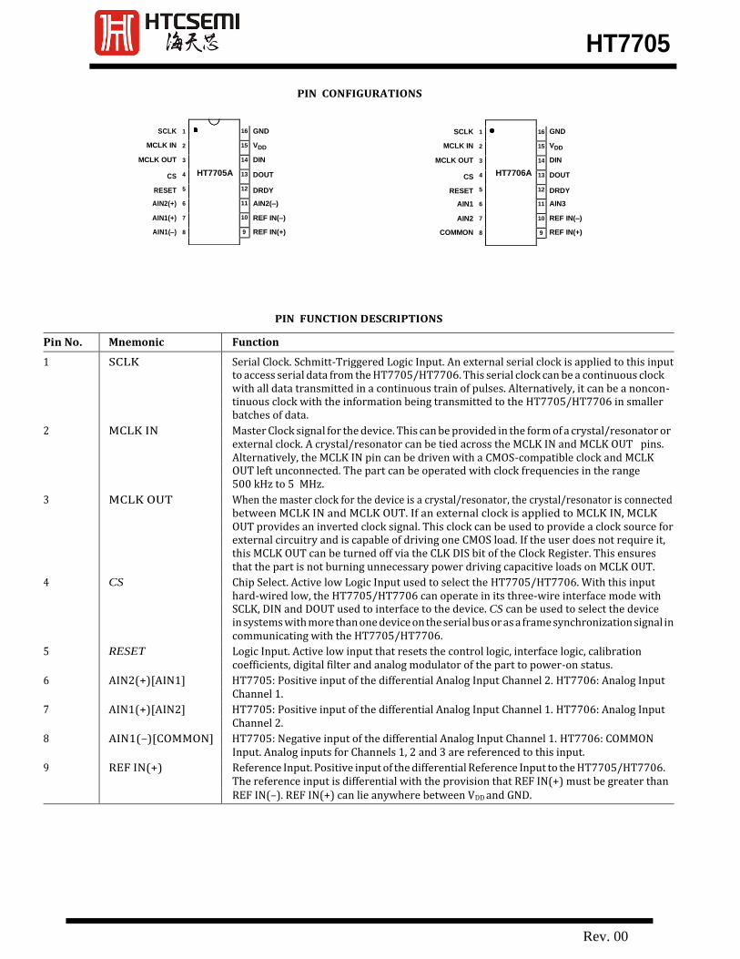
PIN CONFIGURATIONS
SCLK
GND SCLK
GND
MCLK IN VDD MCLK IN VDD
MCLK OUT DIN MCLK OUT DIN
CS DOUT CS DOUT
RESET DRDY RESET DRDY
AIN2(+) AIN2(–) AIN1 AIN3
AIN1(+) REF IN(–) AIN2 REF IN(–)
AIN1(–) REF IN(+) COMMON REF IN(+)
PIN FUNCTION DESCRIPTIONS
Pin No. Mnemonic Function
1 SCLK Serial Clock. Schmitt-Triggered Logic Input. An external serial clock is applied to this input
to access serial data from the HT7705/HT7706. This serial clock can be a continuous clock
with all data transmitted in a continuous train of pulses. Alternatively, it can be a noncon-
tinuous clock with the information being transmitted to the HT7705/HT7706 in smaller
batches of data.
2 MCLK IN Master Clock signal for the device. This can be provided in the form of a crystal/resonator or
external clock. A crystal/resonator can be tied across the MCLK IN and MCLK OUT pins.
Alternatively, the MCLK IN pin can be driven with a CMOS-compatible clock and MCLK
OUT left unconnected. The part can be operated with clock frequencies in the range
500 kHz to 5 MHz.
3 MCLK OUT When the master clock for the device is a crystal/resonator, the crystal/resonator is connected
between MCLK IN and MCLK OUT. If an external clock is applied to MCLK IN, MCLK
OUT provides an inverted clock signal. This clock can be used to provide a clock source for
external circuitry and is capable of driving one CMOS load. If the user does not require it,
this MCLK OUT can be turned off via the CLK DIS bit of the Clock Register. This ensures
that the part is not burning unnecessary power driving capacitive loads on MCLK OUT.
4 CS Chip Select. Active low Logic Input used to select the HT7705/HT7706. With this input
hard-wired low, the HT7705/HT7706 can operate in its three-wire interface mode with
SCLK, DIN and DOUT used to interface to the device. CS can be used to select the device
in systems with more than one device on the serial bus or as a frame synchronization signal in
communicating with the HT7705/HT7706.
5 RESET Logic Input. Active low input that resets the control logic, interface logic, calibration
coefficients, digital filter and analog modulator of the part to power-on status.
6 AIN2(+)[AIN1] HT7705: Positive input of the differential Analog Input Channel 2. HT7706: Analog Input
Channel 1.
7 AIN1(+)[AIN2] HT7705: Positive input of the differential Analog Input Channel 1. HT7706: Analog Input
Channel 2.
8 AIN1(–)[COMMON] HT7705: Negative input of the differential Analog Input Channel 1. HT7706: COMMON
Input. Analog inputs for Channels 1, 2 and 3 are referenced to this input.
9 REF IN(+) Reference Input. Positive input of the differential Reference Input to the HT7705/HT7706.
The reference input is differential with the provision that REF IN(+) must be greater than
REF IN(–). REF IN(+) can lie anywhere between VDD and GND.
1
2
3
4
5
6
7
8
HT7705A
16
15
14
13
12
11
10
9
1
2
3
4
5
6
7
8
HT7706A
16
15
14
13
12
11
10
9
HT7705
Rev. 00
Pin No. Mnemonic Function
10 REF IN(–) Reference Input. Negative input of the differential reference input to the HT7705/HT7706.
The REF IN(–) can lie anywhere between VDD and GND provided REF IN(+) is greater
than REF IN(–).
11 AIN2(–)[AIN3] HT7705: Negative input of the differential analog Input Channel 2. HT7706: Analog Input
Channel 3.
12 DRDY Logic Output. A logic low on this output indicates that a new output word is available from
the HT7705/HT7706 data register. The DRDY pin will return high upon completion of a
read operation of a full output word. If no data read has taken place between output updates,
the DRDY line will return high for 500 tCLK IN cycles prior to the next output update.
While DRDY is high, a read operation should neither be attempted nor in progress to avoid
reading from the data register as it is being updated. The DRDY line will return low again
when the update has taken place. DRDY is also used to indicate when the HT7705/HT7706
has completed its on-chip calibration sequence.
13 DOUT Serial Data Output with serial data being read from the output shift register on the part. This
output shift register can contain information from the setup register, communications regis-
ter, clock register or data register, depending on the register selection bits of the Communica-
tions Register.
14 DIN Serial Data Input with serial data being written to the input shift register on the part. Data
from this input shift register is transferred to the setup register, clock register or communica-
tions register, depending, on the register selection bits of the Communications Register.
15 VDD Supply Voltage, +2.7 V to +5.25 V operation.
16 GND Ground reference point for the HT7705/HT7706’s internal circuitry.
OUTPUT NOISE (5 V OPERATION) Table I shows the HT7705/HT7706 output rms noise for the selectable notch and –3 dB frequencies for the part, as selected by FS0 and FS1 of the Clock Register. The numbers given are for the bipolar input ranges with a VREF of +2.5 V and VDD = 5 V. These numbers are typical and are generated at an analog input voltage of 0 V with the part used in either buffered or unbuffered mode. Table II meanwhile shows the output peak-to-peak noise for the selectable notch and –3 dB frequencies for the part. It is important to note that these numbers represent the resolution for which there will be no code flicker. They are not calculated based on rms noise but on peak-to-peak noise. The numbers given are for bipolar input ranges with a VREF of +2.5 V and for either buffered or unbuffered mode. These num- bers are typical and are rounded to the nearest LSB. The numbers apply for the CLK DIV bit of the Clock Register set to 0.
Table I. Output RMS Noise vs. Gain and Output Update Rate @ 5 V
Filter First Notch and O/P –3 dB Data Rate Frequency
Typical Output RMS Noise in µV
Gain of 1
Gain of 2
Gain of 4
Gain of 8
Gain of 16
Gain of 32
Gain of 64
Gain of 128
MCLK IN = 2.4576 MHz 50 Hz 13.1 Hz 4.1 2.1 1.2 0.75 0.7 0.66 0.63 0.6 60 Hz 15.72 Hz 5.1 2.5 1.4 0.8 0.75 0.7 0.67 0.62 250 Hz 65.5 Hz 110 49 31 17 8 3.6 2.3 1.7 500 Hz 131 Hz 550 285 145 70 41 22 9.1 4.7 MCLK IN = 1 MHz 20 Hz 5.24 Hz 4.1 2.1 1.2 0.75 0.7 0.66 0.63 0.6 25 Hz 6.55 Hz 5.1 2.5 1.4 0.8 0.75 0.7 0.67 0.62 100 Hz 26.2 Hz 110 49 31 17 8 3.6 2.3 1.7 200 Hz 52.4 Hz 550 285 145 70 41 22 9.1 4.7
HT7705
Rev. 00
Filter First Notch and O/P –3 dB Data Rate Frequency
Typical Peak-to-Peak Resolution Bits
Gain of 1
Gain of 2
Gain of 4
Gain of 8
Gain of 16
Gain of 32
Gain of 64
Gain of 128
MCLK IN = 2.4576 MHz 50 Hz 13.1 Hz 16 16 16 16 16 16 15 14 60 Hz 15.72 Hz 16 16 16 16 15 14 14 13 250 Hz 65.5 Hz 13 13 13 13 13 13 12 12 500 Hz 131 Hz 10 10 10 10 10 10 10 10 MCLK IN = 1 MHz 20 Hz 5.24 Hz 16 16 16 16 16 16 15 14 25 Hz 6.55 Hz 16 16 16 16 15 14 14 13 100 Hz 26.2 Hz 13 13 13 13 13 13 12 12 200 Hz 52.4 Hz 10 10 10 10 10 10 10 10
OUTPUT NOISE (3 V OPERATION) Table III shows the HT7705/HT7706 output rms noise for the selectable notch and –3 dB frequencies for the part, as selected by FS0 and FS1 of the Clock Register. The numbers given are for the bipolar input ranges with a VREF of +1.225 V and a VDD = 3 V. These numbers are typical and are generated at an analog input voltage of 0 V with the part used in either buffered or unbuffered mode. Table II meanwhile shows the output peak-to-peak noise for the selectable notch and –3 dB frequencies for the part. It is im- portant to note that these numbers represent the resolution for which there will be no code flicker. They are not calculated based on rms noise but on peak-to-peak noise. The numbers given are for bipolar input ranges with a VREF of +1.225 V and for either buffered or unbuffered mode. These numbers are typical and are rounded to the nearest LSB. The numbers apply for the CLK DIV bit of the Clock Regis- ter set to 0.
Table III. Output RMS Noise vs. Gain and Output Update Rate @ 3 V
Filter First Notch and O/P –3 dB Data Rate Frequency
Typical Output RMS Noise in µV
Gain of 1
Gain of 2
Gain of 4
Gain of 8
Gain of 16
Gain of 32
Gain of 64
Gain of 128
MCLK IN = 2.4576 MHz 50 Hz 13.1 Hz 3.8 2.4 1.5 1.3 1.1 1.0 0.9 0.9 60 Hz 15.72 Hz 5.1 2.9 1.7 1.5 1.2 1.0 0.9 0.9 250 Hz 65.5 Hz 50 25 14 9.9 5.1 2.6 2.3 2.0 500 Hz 131 Hz 270 135 65 41 22 9.7 5.1 3.3 MCLK IN = 1 MHz 20 Hz 5.24 Hz 3.8 2.4 1.5 1.3 1.1 1.0 0.9 0.9 25 Hz 6.55 Hz 5.1 2.9 1.7 1.5 1.2 1.0 0.9 0.9 100 Hz 26.2 Hz 50 25 14 9.9 5.1 2.6 2.3 2.0 200 Hz 52.4 Hz 270 135 65 41 22 9.7 5.1 3.3
Table IV. Peak-to-Peak Resolution vs. Gain and Output Update Rate @ 3 V
Filter First Notch and O/P –3 dB Data Rate Frequency
Typical Peak-to-Peak Resolution in Bits
Gain of 1
Gain of 2
Gain of 4
Gain of 8
Gain of 16
Gain of 32
Gain of 64
Gain of 128
MCLK IN = 2.4576 MHz 50 Hz 13.1 Hz 16 16 15 15 14 13 13 12 60 Hz 15.72 Hz 16 16 15 14 14 13 13 12 250 Hz 65.5 Hz 13 13 13 13 12 12 11 11 500 Hz 131 Hz 10 10 10 10 10 10 10 10 MCLK IN = 1 MHz 20 Hz 5.24 Hz 16 16 15 15 14 13 13 12 25 Hz 6.55 Hz 16 16 15 14 14 13 13 12 100 Hz 26.2 Hz 13 13 13 13 12 12 11 11 200 Hz 52.4 Hz 10 10 10 10 10 10 10 10
HT7705
Rev. 00
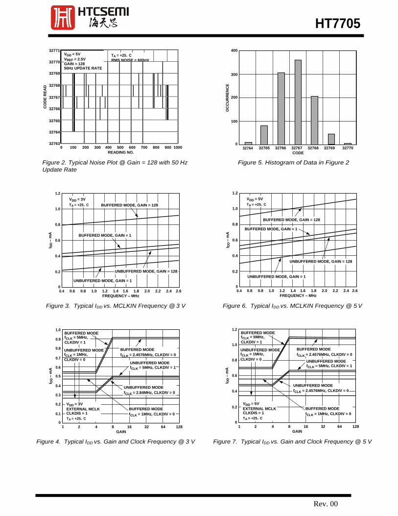
32771
32770
32769
32768
32767
32766
32765
32764
400
300
200
100
32763
0 100
200 300 400 500 600 700 800 900 1000
READING NO.
0 32764
32765 32766 32767 32768 32769 32770
CODE
Figure 2. Typical Noise Plot @ Gain = 128 with 50 Hz
Update Rate
Figure 5. Histogram of Data in Figure 2
1.2
1.0
0.8
0.6
0.4
0.2
1.2
1.0
0.8
0.6
0.4
0.2
0 0.4
0.6 0.8 1.0 1.2 1.4 1.6 1.8 2.0 2.2 2.4 2.6
FREQUENCY – MHz
0 0.4
0.6 0.8 1.0 1.2 1.4 1.6 1.8 2.0 2.2 2.4 2.6
FREQUENCY – MHz
Figure 3. Typical IDD vs. MCLKIN Frequency @ 3 V Figure 6. Typical IDD vs. MCLKIN Frequency @ 5 V
1.0
0.9
0.8
0.7
0.6
0.5
0.4
0.3
0.2
0.1
0 1
2 4 8 16 32 64 128
GAIN
1.2
1.0
0.8
0.6
0.4
0.2
0
1
2 4 8 16 32 64 128
GAIN
Figure 4. Typical IDD vs. Gain and Clock Frequency @ 3 V Figure 7. Typical IDD vs. Gain and Clock Frequency @ 5 V
VDD = 3V
TA = +25。C BUFFERED MODE, GAIN = 128
BUFFERED MODE, GAIN = 1
UNBUFFERED MODE, GAIN = 128
UNBUFFERED MODE, GAIN = 1
BUFFERED MODE fCLK = 5MHz,
CLKDIV = 1
UNBUFFERED MODE fCLK = 1MHz,
CLKDIV = 0
BUFFERED MODE
fCLK = 2.4576MHz, CLKDIV = 0
UNBUFFERED MODE fCLK = 5MHz, CLKDIV = 1
UNBUFFERED MODE
fCLK = 2.84MHz, CLKDIV = 0
VDD = 3V
EXTERNAL MCLK CLKDIS = 1
TA = +25。C
BUFFERED MODE
fCLK = 1MHz, CLKDIV = 0
VDD = 5V
TA = +25。C
BUFFERED MODE, GAIN = 128
BUFFERED MODE, GAIN = 1
UNBUFFERED MODE, GAIN = 128
UNBUFFERED MODE, GAIN = 1
BUFFERED MODE fCLK = 5MHz,
CLKDIV = 1
UNBUFFERED MODE fCLK = 1MHz,
CLKDIV = 0
BUFFERED MODE
fCLK = 2.4576MHz, CLKDIV = 0
UNBUFFERED MODE fCLK = 5MHz, CLKDIV = 1
UNBUFFERED MODE
fCLK = 2.4576MHz, CLKDIV = 0
VDD = 5V
EXTERNAL MCLK CLKDIS = 1
TA = +25。C
BUFFERED MODE
fCLK = 1MHz, CLKDIV = 0
CO
DE
RE
AD
I DD
– m
A
I DD
– m
A
I DD
– m
A
I DD
– m
A
OC
CU
RR
EN
CE
VDD = 5V
VREF = 2.5V
GAIN = 128 50Hz UPDATE RATE
TA = +25。C
RMS NOISE = 600nV
HT7705
Rev. 00
TEK STOP: SINGLE SEQ 50.0kS/s
1
2
2
CH1 5.00V CH2 2.00V
5ms/DIV
20
16
12
8
4
0 –40 –30 –20 –10 0 10 20 30 40 50 60 70 80
TEMPERATURE – 。 C
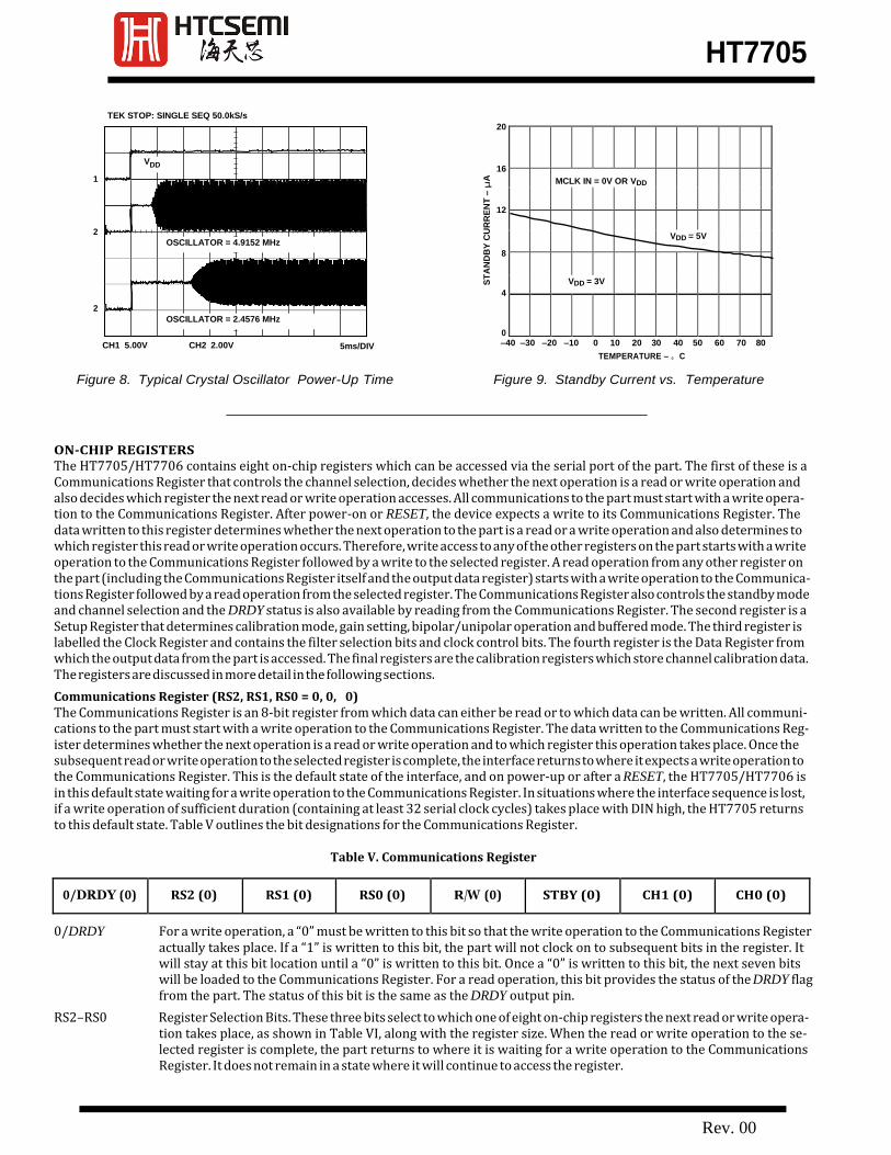
Figure 8. Typical Crystal Oscillator Power-Up Time Figure 9. Standby Current vs. Temperature
ON-CHIP REGISTERS The HT7705/HT7706 contains eight on-chip registers which can be accessed via the serial port of the part. The first of these is a Communications Register that controls the channel selection, decides whether the next operation is a read or write operation and also decides which register the next read or write operation accesses. All communications to the part must start with a write opera- tion to the Communications Register. After power-on or RESET, the device expects a write to its Communications Register. The data written to this register determines whether the next operation to the part is a read or a write operation and also determines to which register this read or write operation occurs. Therefore, write access to any of the other registers on the part starts with a write operation to the Communications Register followed by a write to the selected register. A read operation from any other register on the part (including the Communications Register itself and the output data register) starts with a write operation to the Communica- tions Register followed by a read operation from the selected register. The Communications Register also controls the standby mode and channel selection and the DRDY status is also available by reading from the Communications Register. The second register is a Setup Register that determines calibration mode, gain setting, bipolar/unipolar operation and buffered mode. The third register is labelled the Clock Register and contains the filter selection bits and clock control bits. The fourth register is the Data Register from which the output data from the part is accessed. The final registers are the calibration registers which store channel calibration data. The registers are discussed in more detail in the following sections.
Communications Register (RS2, RS1, RS0 = 0, 0, 0) The Communications Register is an 8-bit register from which data can either be read or to which data can be written. All communi- cations to the part must start with a write operation to the Communications Register. The data written to the Communications Reg- ister determines whether the next operation is a read or write operation and to which register this operation takes place. Once the subsequent read or write operation to the selected register is complete, the interface returns to where it expects a write operation to the Communications Register. This is the default state of the interface, and on power-up or after a RESET, the HT7705/HT7706 is in this default state waiting for a write operation to the Communications Register. In situations where the interface sequence is lost, if a write operation of sufficient duration (containing at least 32 serial clock cycles) takes place with DIN high, the HT7705 returns to this default state. Table V outlines the bit designations for the Communications Register.
Table V. Communications Register
0/DRDY (0) RS2 (0) RS1 (0) RS0 (0) R/W (0) STBY (0) CH1 (0) CH0 (0)
0/DRDY For a write operation, a “0” must be written to this bit so that the write operation to the Communications Register actually takes place. If a “1” is written to this bit, the part will not clock on to subsequent bits in the register. It will stay at this bit location until a “0” is written to this bit. Once a “0” is written to this bit, the next seven bits will be loaded to the Communications Register. For a read operation, this bit provides the status of the DRDY flag from the part. The status of this bit is the same as the DRDY output pin.
RS2–RS0 Register Selection Bits. These three bits select to which one of eight on-chip registers the next read or write opera- tion takes place, as shown in Table VI, along with the register size. When the read or write operation to the se- lected register is complete, the part returns to where it is waiting for a write operation to the Communications Register. It does not remain in a state where it will continue to access the register.
VDD
OSCILLATOR = 4.9152 MHz
OSCILLATOR = 2.4576 MHz
ST
AN
DB
Y C
UR
RE
NT
– µ
A
MCLK IN = 0V OR VDD
VDD = 5V
VDD = 3V
HT7705
Rev. 00
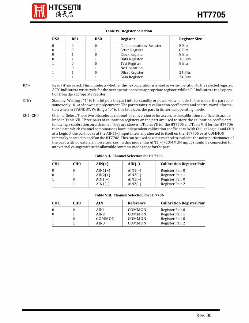
Table VI. Register Selection
RS2 RS1 RS0 Register Register Size
0 0 0 Communications Register 8 Bits 0 0 1 Setup Register 8 Bits 0 1 0 Clock Register 8 Bits 0 1 1 Data Register 16 Bits 1 0 0 Test Register 8 Bits 1 0 1 No Operation 1 1 0 Offset Register 24 Bits 1 1 1 Gain Register 24 Bits
R/W Read/Write Select. This bit selects whether the next operation is a read or write operation to the selected register. A “0” indicates a write cycle for the next operation to the appropriate register, while a “1” indicates a read opera- tion from the appropriate register.
STBY Standby. Writing a “1” to this bit puts the part into its standby or power-down mode. In this mode, the part con- sumes only 10 A of power supply current. The part retains its calibration coefficients and control word informa- tion when in STANDBY. Writing a “0” to this bit places the part in its normal operating mode.
CH1–CH0 Channel Select. These two bits select a channel for conversion or for access to the calibration coefficients as out- lined in Table VII. Three pairs of calibration registers on the part are used to store the calibration coefficients following a calibration on a channel. They are shown in Tables VII for the HT7705 and Table VIII for the HT7706 to indicate which channel combinations have independent calibration coefficients. With CH1 at Logic 1 and CH0 at a Logic 0, the part looks at the AIN1(–) input internally shorted to itself on the HT7705 or at COMMON internally shorted to itself on the HT7706. This can be used as a test method to evaluate the noise performance of the part with no external noise sources. In this mode, the AIN1(–)/COMMON input should be connected to an external voltage within the allowable common-mode range for the part.
Table VII. Channel Selection for HT7705
CH1 CH0 AIN(+) AIN(–) Calibration Register Pair
0 0 AIN1(+) AIN1(–) Register Pair 0 0 1 AIN2(+) AIN2(–) Register Pair 1 1 0 AIN1(–) AIN1(–) Register Pair 0 1 1 AIN1(–) AIN2(–) Register Pair 2
Table VIII. Channel Selection for HT7706
CH1 CH0 AIN Reference Calibration Register Pair
0 0 AIN1 COMMON Register Pair 0 0 1 AIN2 COMMON Register Pair 1 1 0 COMMON COMMON Register Pair 0 1 1 AIN3 COMMON Register Pair 2
HT7705
Rev. 00
Setup Register (RS2, RS1, RS0 = 0, 0, 1); Power-On/Reset Status: 01 Hex The Setup Register is an eight bit register from which data can either be read or to which data can be written. Table IX outlines the bit designations for the Setup Register.
Table IX. Setup Register
MD1 (0) MD0 (0) G2 (0) G1 (0) G0 (0) B/U (0) BUF (0) FSYNC (1)
MD1 MD0 Operating Mode
0 0 Normal Mode: this is the normal mode of operation of the device whereby the device is performing normal
conversions.
0 1 Self-Calibration: this activates self-calibration on the channel selected by CH1 and CH0 of the Communica-
tions Register. This is a one-step calibration sequence and when complete the part returns to Normal Mode
with MD1 and MD0 returning to 0, 0. The DRDY output or bit goes high when calibration is initiated and
returns low when this self-calibration is complete and a new valid word is available in the data register. The
zero-scale calibration is performed at the selected gain on internally shorted (zeroed) inputs and the full-
scale calibration is performed at the selected gain on an internally-generated VREF/Selected Gain.
1 0 Zero-Scale System Calibration: this activates zero scale system calibration on the channel selected by CH1
and CH0 of the Communications Register. Calibration is performed at the selected gain on the input volt-
age provided at the analog input during this calibration sequence. This input voltage should remain stable
for the duration of the calibration. The DRDY output or bit goes high when calibration is initiated and
returns low when this zero-scale calibration is complete and a new valid word is available in the data register.
At the end of the calibration, the part returns to Normal Mode with MD1 and MD0 returning to 0, 0.
1 1 Full-Scale System Calibration: this activates full-scale system calibration on the selected input channel.
Calibration is performed at the selected gain on the input voltage provided at the analog input during this
calibration sequence. This input voltage should remain stable for the duration of the calibration. Once
again, the DRDY output or bit goes high when calibration is initiated and returns low when this full-scale
calibration is complete and a new valid word is available in the data register. At the end of the calibration,
the part returns to Normal Mode with MD1 and MD0 returning to 0, 0.
G2–G0 Gain Selection Bits. These bits select the gain setting for the on-chip PGA as outlined in Table X.
Table X. Gain Selection
G2 G1 G0 Gain Setting
0 0 0 1 0 0 1 2 0 1 0 4 0 1 1 8 1 0 0 16 1 0 1 32 1 1 0 64 1 1 1 128
B/U Bipolar/Unipolar Operation. A “0” in this bit selects Bipolar Operation. A “1” in this bit selects Unipolar Operation.
BUF Buffer Control. With this bit at “0,” the on-chip buffer on the analog input is shorted out. With the buffer shorted out, the current flowing in the VDD line is reduced. When this bit is high, the on-chip buffer is in series with the analog input allowing the input to handle higher source impedances.
FSYNC Filter Synchronization. When this bit is high, the nodes of the digital filter, the filter control logic and the calibra- tion control logic are held in a reset state and the analog modulator is also held in its reset state. When this bit goes low, the modulator and filter start to process data and a valid word is available in 3 1/(output update rate), i.e., the settling time of the filter. This FSYNC bit does not affect the digital interface and does not reset the DRDY output if it is low.
HT7705
Rev. 00
Clock Register (RS2, RS1, RS0 = 0, 1, 0); Power-On/Reset Status: 05 Hex The Clock Register is an 8-bit register from which data can either be read or to which data can be written. Table XI outlines the bit designations for the Clock Register.
Table XI. Clock Register
ZERO (0) ZERO (0) ZERO (0) CLKDIS (0) CLKDIV (0) CLK (1) FS1 (0) FS0 (1)
ZERO Zero. A zero MUST be written to these bits to ensure correct operation of the HT7705/HT7706. Failure to do so
may result in unspecified operation of the device.
CLKDIS Master Clock Disable Bit. A Logic 1 in this bit disables the master clock from appearing at the MCLK OUT pin. When disabled, the MCLK OUT pin is forced low. This feature allows the user the flexibility of using the MCLK OUT as a clock source for other devices in the system or of turning off the MCLK OUT as a power saving feature. When using an external master clock on the MCLK IN pin, the HT7705/HT7706 continues to have internal clocks and will convert normally with the CLKDIS bit active. When using a crystal oscillator or ceramic resonator across the MCLK IN and MCLK OUT pins, the HT7705/HT7706 clock is stopped and no conversions take place when the CLKDIS bit is active.
CLKDIV Clock Divider Bit. With this bit at a Logic 1, the clock frequency appearing at the MCLK IN pin is divided by two before being used internally by the HT7705/HT7706. For example, when this bit is set to 1, the user can operate with a 4.9152 MHz crystal between MCLK IN and MCLK OUT and internally the part will operate with the specified 2.4576 MHz. With this bit at a Logic 0, the clock frequency appearing at the MCLK IN pin is the fre- quency used internally by the part.
CLK Clock Bit. This bit should be set in accordance with the operating frequency of the HT7705/HT7706. If the device has a master clock frequency of 2.4576 MHz (CLKDIV = 0) or 4.9152 MHz (CLKDIV = 1), then this bit should be set to a “1.” If the device has a master clock frequency of 1 MHz (CLKDIV = 0) or 2 MHz (CLKDIV = 1), this bit should be set to a “0.” This bit sets up the appropriate scaling currents for a given operating frequency and also chooses (along with FS1 and FS0) the output update rate for the device. If this bit is not set correctly for the master clock frequency of the device, then the HT7705/HT7706 may not operate to specification.
FS1, FS0 Filter Selection Bits. Along with the CLK bit, FS1 and FS0 determine the output update rate, filter first notch and –3 dB frequency as outlined in Table XII. The on-chip digital filter provides a sinc3 (or Sinx/x3) filter response. In association with the gain selection, it also determines the output noise of the device. Changing the filter notch frequency, as well as the selected gain, impacts resolution. Tables I to IV show the effect of filter notch frequency and gain on the output noise and effective resolution of the part. The output data rate (or effective conversion time) for the device is equal to the frequency selected for the first notch of the filter. For example, if the first notch of the filter is selected at 50 Hz, a new word is available at a 50 Hz output rate or every 20 ms. If the first notch is at 500 Hz, a new word is available every 2 ms. A calibration should be initiated when any of these bits are changed.
The settling time of the filter to a full-scale step input is worst case 4 1/(output data rate). For example, with the filter first notch at 50 Hz, the settling time of the filter to a full-scale step input is 80 ms max. If the first notch is at 500 Hz, the settling time is 8 ms max. This settling time can be reduced to 3 1/(output data rate) by synchroniz- ing the step input change to a reset of the digital filter. In other words, if the step input takes place with the FSYNC bit high, the settling-time will be 3 1/(output data rate) from when the FSYNC bit returns low.
The –3 dB frequency is determined by the programmed first notch frequency according to the relationship:
filter –3 dB frequency = 0.262 filter first notch frequency
Table XII. Output Update Rates
CLK* FS1 FS0 Output Update Rate –3 dB Filter Cutoff
0 0 0 20 Hz 5.24 Hz 0 0 1 25 Hz 6.55 Hz 0 1 0 100 Hz 26.2 Hz 0 1 1 200 Hz 52.4 Hz 1 0 0 50 Hz 13.1 Hz 1 0 1 60 Hz 15.7 Hz 1 1 0 250 Hz 65.5 Hz 1 1 1 500 Hz 131 Hz
*Assumes correct clock frequency on MCLK IN pin with CLKDIV bit set appropriately.
HT7705
Rev. 00
Data Register (RS2, RS1, RS0 = 0, 1, 1) The Data Register on the part is a 16-bit read-only register that contains the most up-to-date conversion result from the HT7705/ HT7706. If the Communications Register sets up the part for a write operation to this register, a write operation must actually take place to return the part to where it is expecting a write operation to the Communications Register. However, the 16 bits of data written to the part will be ignored by the HT7705/HT7706.
Test Register (RS2, RS1, RS0 = 1, 0, 0); Power-On/Reset Status: 00 Hex The part contains a Test Register that is used when testing the device. The user is advised not to change the status of any of the bits in this register from the default (Power-on or RESET) status of all 0s as the part will be placed in one of its test modes and will not operate correctly.
Zero-Scale Calibration Register (RS2, RS1, RS0 = 1, 1, 0); Power-On/Reset Status: 1F4000 Hex The HT7705/HT7706 contains independent sets of zero-scale registers, one for each of the input channels. Each of these registers is a 24-bit read/write register; 24 bits of data must be written otherwise no data will be transferred to the register. This register is used in conjunction with its associated full-scale register to form a register pair. These register pairs are associated with input channel pairs as outlined in Table VII. While the part is set up to allow access to these registers over the digital interface, the part itself no longer has access to the register coefficients to correctly scale the output data. As a result, there is a possibility that after accessing the calibration registers (either read or write operation) the first output data read from the part may contain incorrect data. In addition, a write to the calibration register should not be attempted while a calibration is in progress. These eventualities can be avoided by taking the FSYNC bit in the mode register high before the calibration register operation and taking it low after the operation is complete.
Full-Scale Calibration Register (RS2, RS1, RS0 = 1, 1, 1); Power-On/Reset Status: 5761AB Hex The HT7705/HT7706 contains independent sets of full-scale registers, one for each of the input channels. Each of these registers is a 24-bit read/write register; 24 bits of data must be written otherwise no data will be transferred to the register. This register is used in conjunction with its associated zero-scale register to form a register pair. These register pairs are associated with input channel pairs as outlined in Table VII. While the part is set up to allow access to these registers over the digital interface, the part itself no longer has access to the register coefficients to correctly scale the output data. As a result, there is a possibility that after accessing the cali- bration registers (either read or write operation) the first output data read from the part may contain incorrect data. In addition, a write to the calibration register should not be attempted while a calibration is in progress. These eventualities can be avoided by taking FSYNC bit in the mode register high before the calibration register operation and taking it low after the operation is complete.
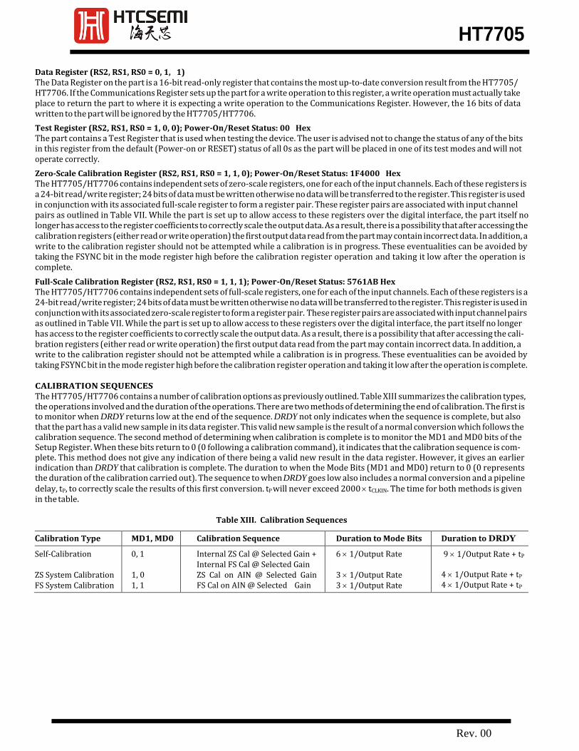
CALIBRATION SEQUENCES The HT7705/HT7706 contains a number of calibration options as previously outlined. Table XIII summarizes the calibration types, the operations involved and the duration of the operations. There are two methods of determining the end of calibration. The first is to monitor when DRDY returns low at the end of the sequence. DRDY not only indicates when the sequence is complete, but also that the part has a valid new sample in its data register. This valid new sample is the result of a normal conversion which follows the calibration sequence. The second method of determining when calibration is complete is to monitor the MD1 and MD0 bits of the Setup Register. When these bits return to 0 (0 following a calibration command), it indicates that the calibration sequence is com- plete. This method does not give any indication of there being a valid new result in the data register. However, it gives an earlier indication than DRDY that calibration is complete. The duration to when the Mode Bits (MD1 and MD0) return to 0 (0 represents the duration of the calibration carried out). The sequence to when DRDY goes low also includes a normal conversion and a pipeline delay, tP, to correctly scale the results of this first conversion. tP will never exceed 2000 tCLKIN. The time for both methods is given in the table.
Table XIII. Calibration Sequences
Calibration Type MD1, MD0 Calibration Sequence Duration to Mode Bits Duration to DRDY
Self-Calibration
ZS System Calibration FS System Calibration
0, 1
1, 0 1, 1
Internal ZS Cal @ Selected Gain + Internal FS Cal @ Selected Gain ZS Cal on AIN @ Selected Gain FS Cal on AIN @ Selected Gain
6 1/Output Rate
3 1/Output Rate 3 1/Output Rate
9 1/Output Rate + tP
4 1/Output Rate + tP
4 1/Output Rate + tP
HT7705
Rev. 00
VDD
AIN1(+)
AIN1(–)
HT7705
DRDY
DOUT
AIN2(+)
AIN2(–) DIN
SCLK
GND
RESET
REF IN(+) CS
REF IN(–) MCLK IN
MCLK OUT
VIN
VOUT
AD780/ REF192
GND
CIRCUIT DESCRIPTION The HT7705/HT7706 is a sigma-delta A/D converter with on- chip digital filtering, intended for the measurement of wide dynamic range, low frequency signals such as those in industrial control or process control applications. It contains a sigma-delta (or charge-balancing) ADC, a calibration microcontroller with on-chip static RAM, a clock oscillator, a digital filter and a bi- directional serial communications port. The part consumes only 320 A of power supply current, making it ideal for battery- powered or loop-powered instruments. These parts operate with a supply voltage of 2.7 V to 3.3 V or 4.75 V to 5.25 V.
The HT7705 contains two programmable-gain fully differential analog input channels, while the HT7706 contains three pseudo differential analog input channels. The selectable gains on these inputs are 1, 2, 4, 8, 16, 32, 64 and 128 allowing the part to accept unipolar signals of between 0 mV to +20 mV and 0 V to +2.5 V, or bipolar signals in the range from 20 mV to 2.5 V when the reference input voltage equals +2.5 V. With a refer- ence voltage of +1.225 V, the input ranges are from 0 mV to +10 mV to 0 V to +1.225 V in unipolar mode, and from 10 mV to 1.225 V in bipolar mode. Note that the bipolar ranges are with respect to AIN(–) on the HT7705, and with respect to COMMON on the HT7706, and not with respect to GND.
The input signal to the analog input is continuously sampled at a rate determined by the frequency of the master clock, MCLK IN, and the selected gain. A charge-balancing A/D converter (Sigma-Delta Modulator) converts the sampled signal into a digital pulse train whose duty cycle contains the digital information. The programmable gain function on the analog
input is also incorporated in this sigma-delta modulator with the input sampling frequency being modified to give the higher gains. A sinc3 digital low-pass filter processes the output of the sigma-delta modulator and updates the output register at a rate determined by the first notch frequency of this filter. The out- put data can be read from the serial port randomly or periodi- cally at any rate up to the output register update rate. The first notch of this digital filter (and hence its –3 dB frequency) can be programmed via the Setup Register bits FS0 and FS1. With a master clock frequency of 2.4576 MHz, the programmable range for this first notch frequency is from 50 Hz to 500 Hz, giving a programmable range for the –3 dB frequency of 13.1 Hz to 131 Hz. With a master clock frequency of 1 MHz, the programmable range for this first notch frequency is from 20 Hz to 200 Hz, giving a programmable range for the –3 dB frequency of 5.24 Hz to 52.4 Hz.
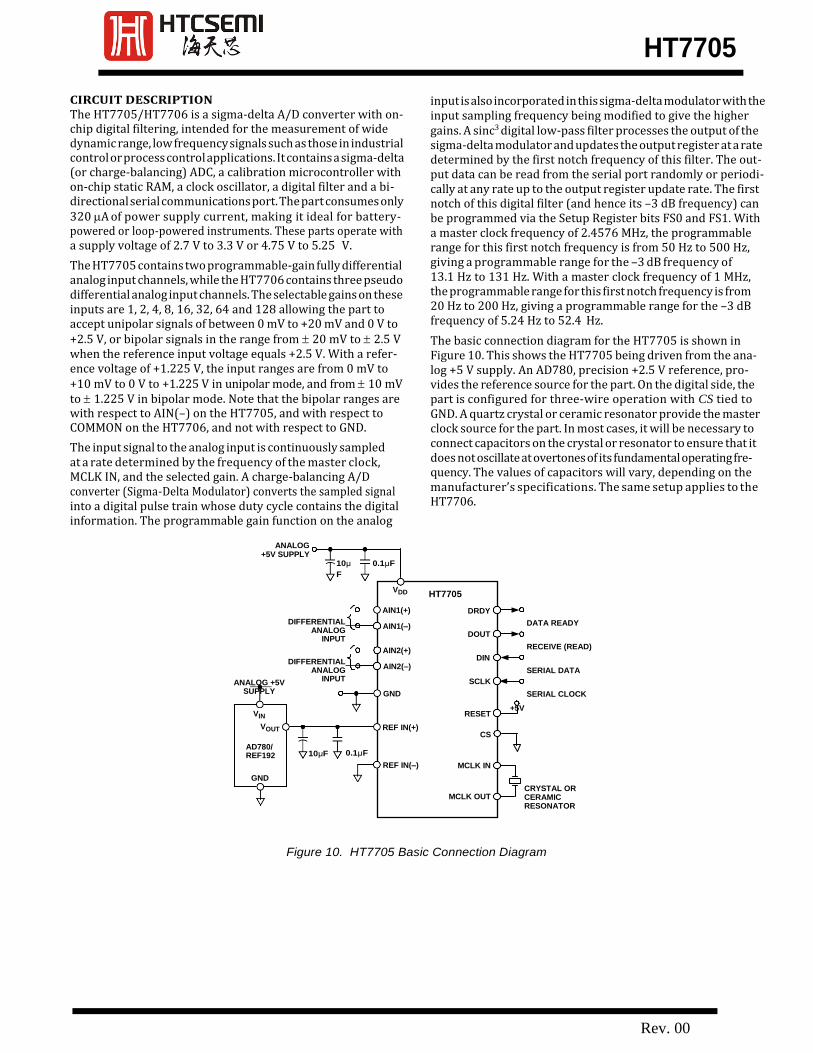
The basic connection diagram for the HT7705 is shown in Figure 10. This shows the HT7705 being driven from the ana- log +5 V supply. An AD780, precision +2.5 V reference, pro- vides the reference source for the part. On the digital side, the part is configured for three-wire operation with CS tied to GND. A quartz crystal or ceramic resonator provide the master clock source for the part. In most cases, it will be necessary to connect capacitors on the crystal or resonator to ensure that it does not oscillate at overtones of its fundamental operating fre- quency. The values of capacitors will vary, depending on the manufacturer’s specifications. The same setup applies to the HT7706.
ANALOG +5V SUPPLY
10µ
F
0.1µF
ANALOG +5V
SUPPLY
DIFFERENTIAL ANALOG
INPUT
DIFFERENTIAL ANALOG
INPUT
+5V
DATA READY
RECEIVE (READ)
SERIAL DATA
SERIAL CLOCK
10µF 0.1µF
CRYSTAL OR CERAMIC RESONATOR
Figure 10. HT7705 Basic Connection Diagram
HT7705
Rev. 00
ANALOG INPUT Analog Input Ranges The HT7705 contains two differential analog input pairs AIN1(+), AIN1(–) and AIN2(+), AIN2(–). These input pairs provide programmable-gain, differential input channels that can handle either unipolar or bipolar input signals. It should be noted that the bipolar input signals are referenced to the re- spective AIN(–) input of each input pair. The HT7706 contains three pseudo differential analog input pairs AIN1, AIN2 and AIN3, which are referenced to the COMMON input on the part.
In unbuffered mode, the common-mode range of the input is from GND to VDD, provided that the absolute value of the analog input voltage lies between GND – 30 mV and VDD
+ 30 mV. This means that in unbuffered mode the part can handle both unipolar and bipolar input ranges for all gains. Absolute voltages of GND – 200 mV can be accommodated on the analog inputs at 25C without degradation in performance, but leakage current increases appreciably with increasing tem- perature. In buffered mode, the analog inputs can handle much larger source impedances, but the absolute input voltage range is restricted to between GND + 50 mV to VDD – 1.5 V which also places restrictions on the common-mode range. This means that in buffered mode there are some restrictions on the allowable gains for bipolar input ranges. Care must be taken in setting up the common-mode voltage and input voltage range so that the above limits are not exceeded, otherwise there will be a degradation in linearity performance.
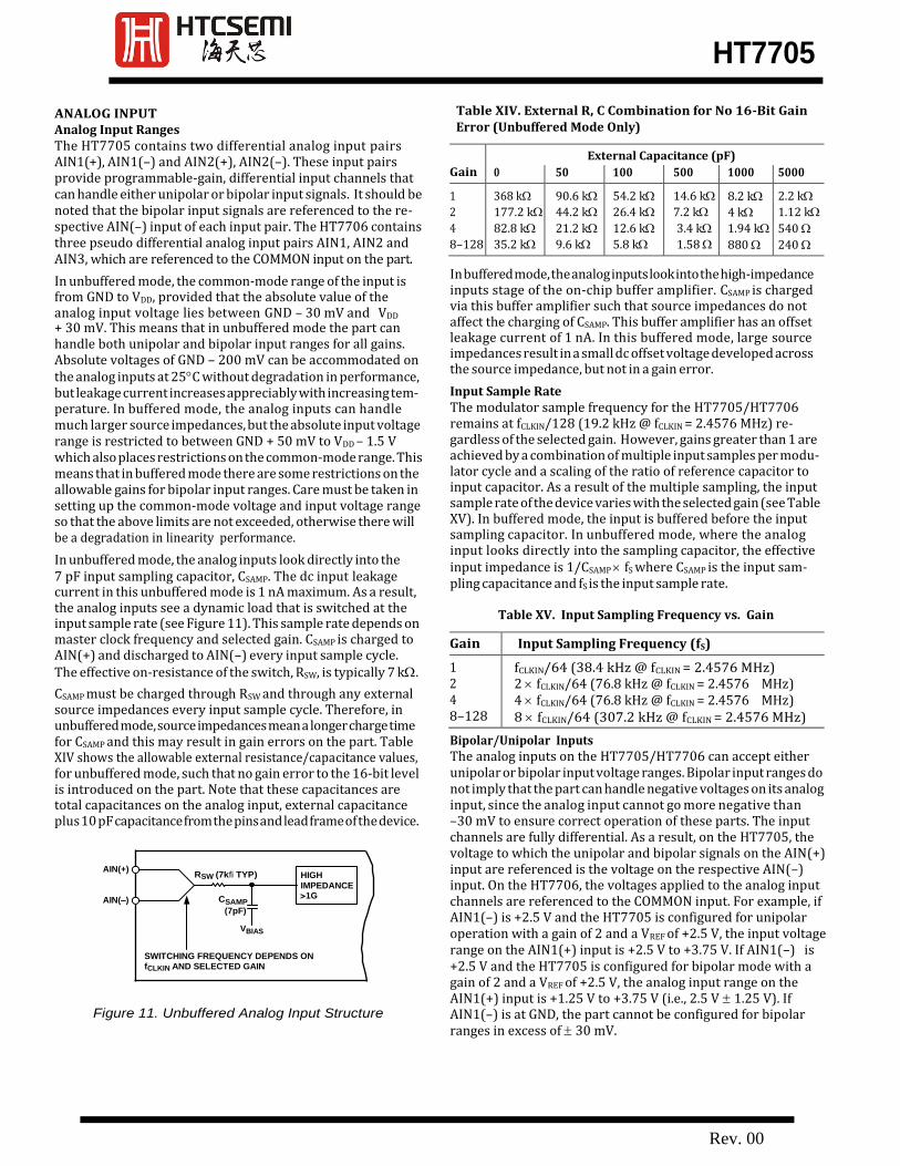
In unbuffered mode, the analog inputs look directly into the 7 pF input sampling capacitor, CSAMP. The dc input leakage current in this unbuffered mode is 1 nA maximum. As a result, the analog inputs see a dynamic load that is switched at the input sample rate (see Figure 11). This sample rate depends on master clock frequency and selected gain. CSAMP is charged to AIN(+) and discharged to AIN(–) every input sample cycle. The effective on-resistance of the switch, RSW, is typically 7 k.
CSAMP must be charged through RSW and through any external source impedances every input sample cycle. Therefore, in unbuffered mode, source impedances mean a longer charge time for CSAMP and this may result in gain errors on the part. Table XIV shows the allowable external resistance/capacitance values, for unbuffered mode, such that no gain error to the 16-bit level is introduced on the part. Note that these capacitances are total capacitances on the analog input, external capacitance plus 10 pF capacitance from the pins and lead frame of the device.
AIN(+)
AIN(–)
Figure 11. Unbuffered Analog Input Structure
Table XIV. External R, C Combination for No 16-Bit Gain Error (Unbuffered Mode Only)
Gain
External Capacitance (pF)
0 50 100 500 1000 5000
1
2
4
8–128
368 k
177.2 k
82.8 k
35.2 k
90.6 k
44.2 k
21.2 k
9.6 k
54.2 k
26.4 k
12.6 k
5.8 k
14.6 k
7.2 k
3.4 k
1.58
8.2 k
4 k
1.94 k
880
2.2 k
1.12 k
540
240
In buffered mode, the analog inputs look into the high-impedance inputs stage of the on-chip buffer amplifier. CSAMP is charged via this buffer amplifier such that source impedances do not affect the charging of CSAMP. This buffer amplifier has an offset leakage current of 1 nA. In this buffered mode, large source impedances result in a small dc offset voltage developed across the source impedance, but not in a gain error.
Input Sample Rate The modulator sample frequency for the HT7705/HT7706 remains at fCLKIN/128 (19.2 kHz @ fCLKIN = 2.4576 MHz) re- gardless of the selected gain. However, gains greater than 1 are achieved by a combination of multiple input samples per modu- lator cycle and a scaling of the ratio of reference capacitor to input capacitor. As a result of the multiple sampling, the input sample rate of the device varies with the selected gain (see Table XV). In buffered mode, the input is buffered before the input sampling capacitor. In unbuffered mode, where the analog input looks directly into the sampling capacitor, the effective input impedance is 1/CSAMP fS where CSAMP is the input sam- pling capacitance and fS is the input sample rate.
Table XV. Input Sampling Frequency vs. Gain
Gain Input Sampling Frequency (fS)
1 2 4 8–128
fCLKIN/64 (38.4 kHz @ fCLKIN = 2.4576 MHz) 2 fCLKIN/64 (76.8 kHz @ fCLKIN = 2.4576 MHz) 4 fCLKIN/64 (76.8 kHz @ fCLKIN = 2.4576 MHz) 8 fCLKIN/64 (307.2 kHz @ fCLKIN = 2.4576 MHz)
Bipolar/Unipolar Inputs The analog inputs on the HT7705/HT7706 can accept either unipolar or bipolar input voltage ranges. Bipolar input ranges do not imply that the part can handle negative voltages on its analog input, since the analog input cannot go more negative than –30 mV to ensure correct operation of these parts. The input channels are fully differential. As a result, on the HT7705, the voltage to which the unipolar and bipolar signals on the AIN(+) input are referenced is the voltage on the respective AIN(–) input. On the HT7706, the voltages applied to the analog input channels are referenced to the COMMON input. For example, if AIN1(–) is +2.5 V and the HT7705 is configured for unipolar operation with a gain of 2 and a VREF of +2.5 V, the input voltage range on the AIN1(+) input is +2.5 V to +3.75 V. If AIN1(–) is +2.5 V and the HT7705 is configured for bipolar mode with a gain of 2 and a VREF of +2.5 V, the analog input range on the AIN1(+) input is +1.25 V to +3.75 V (i.e., 2.5 V 1.25 V). If AIN1(–) is at GND, the part cannot be configured for bipolar ranges in excess of 30 mV.
HIGH
IMPEDANCE 1G
RSW (7kfi TYP)
CSAMP
(7pF)
VBIAS
SWITCHING FREQUENCY DEPENDS ON fCLKIN AND SELECTED GAIN
HT7705
Rev. 00
Bipolar or unipolar options are chosen by programming the B/U bit of the Setup Register. This programs the channel for either unipolar or bipolar operation. Programming the channel for either unipolar or bipolar operation does not change any of the input signal conditioning, it simply changes the data output coding and the points on the transfer function where calibra- tions occur.
REFERENCE INPUT The HT7705/HT7706’s reference inputs, REF IN(+) and REF IN(–), provide a differential reference input capability. The common-mode range for these differential inputs is from GND to VDD. The nominal reference voltage, VREF (REF IN(+) – REF IN(–)), for specified operation, is +2.5 V for the HT7705/ HT7706 operated with a VDD of 5 V and +1.225 V for the HT7705/HT7706 operated with a VDD of 3 V. The part is func- tional with VREF voltages down to 1 V, but with degraded per- formance as the output noise will, in terms of LSB size, be larger. REF IN(+) must always be greater than REF IN(–) for correct operation of the HT7705/HT7706.
Both reference inputs provide a high impedance, dynamic load similar to the analog inputs in unbuffered mode. The maximum dc input leakage current is 1 nA over temperature, and source resistance may result in gain errors on the part. In this case, the sampling switch resistance is 5 k typ and the reference capaci- tor (CREF) varies with gain. The sample rate on the reference inputs is fCLKIN/64 and does not vary with gain. For gains of 1 and 2, CREF is 8 pF; for a gain of 16, it is 5.5 pF, for a gain of 32, it is 4.25 pF, for a gain of 64, it is 3.625 pF and for a gain of 128, it is 3.3125 pF.
The output noise performance outlined in Tables I through IV is for an analog input of 0 V, which effectively removes the effect of noise on the reference. To obtain the same noise per- formance as shown in the noise tables over the full input range requires a low noise reference source for the HT7705/HT7706. If the reference noise in the bandwidth of interest is excessive, it will degrade the performance of the HT7705/HT7706. In appli- cations where the excitation voltage for the bridge transducer on the analog input also derives the reference voltage for the part, the effect of the noise in the excitation voltage will be removed as the application is ratiometric. Recommended reference volt- age sources for the HT7705 with a VDD of 5 V include the AD780, REF43 and REF192, while the recommended reference sources for the HT7705 operated with a VDD of 3 V include the AD589 and AD1580. It is generally recommended to decouple the output of these references in order to further reduce the noise level.
DIGITAL FILTERING The HT7705/HT7706 contains an on-chip low-pass digital filter which processes the output of the part’s sigma-delta modulator. Therefore, the part not only provides the analog-to-digital con- version function but also provides a level of filtering. There are a number of system differences when the filtering function is provided in the digital domain rather than the analog domain and the user should be aware of these.
First, since digital filtering occurs after the A-to-D conversion process, it can remove noise injected during the conversion process. Analog filtering cannot do this. Also, the digital filter can be made programmable far more readily than an analog filter. Depending on the digital filter design, this gives the user
the capability of programming cutoff frequency and output update rate.
On the other hand, analog filtering can remove noise superim- posed on the analog signal before it reaches the ADC. Digital filtering cannot do this and noise peaks riding on signals near full scale have the potential to saturate the analog modulator and digital filter, even though the average value of the signal is within limits. To alleviate this problem, the HT7705/HT7706 has overrange headroom built into the sigma-delta modulator and digital filter, which allows overrange excursions of 5% above the analog input range. If noise signals are larger than this, consideration should be given to analog input filtering, or to reducing the input channel voltage so that its full-scale is half that of the analog input channel full-scale. This will provide an overrange capability greater than 100% at the expense of reduc- ing the dynamic range by 1 bit (50%).
In addition, the digital filter does not provide any rejection at integer multiples of the digital filter’s sample frequency. How- ever, the input sampling on the part provides attenuation at multiples of the digital filter’s sampling frequency so that the unattenuated bands actually occur around multiples of the sampling frequency fS (as defined in Table XV). Thus the unattenuated bands occur at n fS (where n = 1, 2, 3 . . .). At these frequencies, there are frequency bands, f3 dB wide f3 dB is the cutoff frequency of the digital filter) at either side where noise passes unattenuated to the output.
Filter Characteristics The HT7705/HT7706’s digital filter is a low-pass filter with a (sinx/x)3 response (also called sinc3). The transfer function for this filter is described in the z-domain by:
H(z) 1
1 Z –N
N 1 Z –1
and in the frequency domain by:
H( f ) 1
SIN(N f /f S ) N SIN( f /f S )
where N is the ratio of the modulator rate to the output rate.
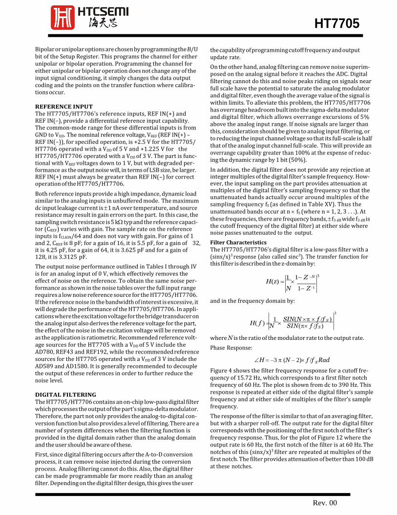
Phase Response:
H –3 (N – 2) f /f S Rad
Figure 4 shows the filter frequency response for a cutoff fre- quency of 15.72 Hz, which corresponds to a first filter notch frequency of 60 Hz. The plot is shown from dc to 390 Hz. This response is repeated at either side of the digital filter’s sample frequency and at either side of multiples of the filter’s sample frequency.
The response of the filter is similar to that of an averaging filter, but with a sharper roll-off. The output rate for the digital filter corresponds with the positioning of the first notch of the filter’s frequency response. Thus, for the plot of Figure 12 where the output rate is 60 Hz, the first notch of the filter is at 60 Hz. The notches of this (sinx/x)3 filter are repeated at multiples of the first notch. The filter provides attenuation of better than 100 dB at these notches.
3
3
HT7705
Rev. 00
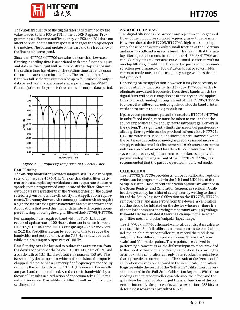
The cutoff frequency of the digital filter is determined by the value loaded to bits FS0 to FS1 in the CLOCK Register. Pro- gramming a different cutoff frequency via FS0 and FS1 does not alter the profile of the filter response, it changes the frequency of the notches. The output update of the part and the frequency of the first notch correspond.
Since the HT7705/HT7706 contains this on-chip, low-pass filtering, a settling time is associated with step function inputs and data on the output will be invalid after a step change until the settling time has elapsed. The settling time depends upon the output rate chosen for the filter. The settling time of the filter to a full-scale step input can be up to four times the output data period. For a synchronized step input (using the FSYNC function), the settling time is three times the output data period.
0
–20
–40
–60
–80
–100
–120
–140
–160
–180
–200
–220
ANALOG FILTERING The digital filter does not provide any rejection at integer mul- tiples of the modulator sample frequency, as outlined earlier. However, due to the HT7705/HT7706’s high oversampling ratio, these bands occupy only a small fraction of the spectrum and most broadband noise is filtered. This means that the ana- log filtering requirements in front of the HT7705/HT7706 are considerably reduced versus a conventional converter with no on-chip filtering. In addition, because the part’s common-mode rejection performance of 100 dB extends out to several kHz, common-mode noise in this frequency range will be substan- tially reduced.
Depending on the application, however, it may be necessary to provide attenuation prior to the HT7705/HT7706 in order to eliminate unwanted frequencies from these bands which the digital filter will pass. It may also be necessary in some applica- tions to provide analog filtering in front of the HT7705/HT7706 to ensure that differential noise signals outside the band of inter- est do not saturate the analog modulator.
If passive components are placed in front of the HT7705/HT7706 in unbuffered mode, care must be taken to ensure that the source impedance is low enough not to introduce gain errors in the system. This significantly limits the amount of passive anti- aliasing filtering which can be provided in front of the HT7705/ HT7706 when it is used in unbuffered mode. However, when the part is used in buffered mode, large source impedances will simply result in a small dc offset error (a 10 k source resistance will cause an offset error of less than 10 V). Therefore, if the
–240 0 60 120 180 240 300 360
FREQUENCY – Hz
system requires any significant source impedances to provide passive analog filtering in front of the HT7705/HT7706, it is
Figure 12. Frequency Response of HT7705 Filter
Post-Filtering The on-chip modulator provides samples at a 19.2 kHz output rate with fCLKIN at 2.4576 MHz. The on-chip digital filter deci- mates these samples to provide data at an output rate that corre- sponds to the programmed output rate of the filter. Since the output data rate is higher than the Nyquist criterion, the output rate for a given bandwidth will satisfy most application require- ments. There may, however, be some applications which require a higher data rate for a given bandwidth and noise performance. Applications that need this higher data rate will require some post-filtering following the digital filter of the HT7705/HT7706.
For example, if the required bandwidth is 7.86 Hz, but the required update rate is 100 Hz, the data can be taken from the HT7705/HT7706 at the 100 Hz rate giving a –3 dB bandwidth of 26.2 Hz. Post-filtering can be applied to this to reduce the bandwidth and output noise, to the 7.86 Hz bandwidth level, while maintaining an output rate of 100 Hz.
Post-filtering can also be used to reduce the output noise from the device for bandwidths below 13.1 Hz. At a gain of 128 and a bandwidth of 13.1 Hz, the output rms noise is 450 nV. This is essentially device noise or white noise and since the input is chopped, the noise has a primarily flat frequency response. By reducing the bandwidth below 13.1 Hz, the noise in the result- ant passband can be reduced. A reduction in bandwidth by a factor of 2 results in a reduction of approximately 1.25 in the output rms noise. This additional filtering will result in a longer settling-time.
recommended that the part be operated in buffered mode.
CALIBRATION The HT7705/HT7706 provides a number of calibration options which can be programmed via the MD1 and MD0 bits of the Setup Register. The different calibration options are outlined in the Setup Register and Calibration Sequences sections. A cali- bration cycle may be initiated at any time by writing to these bits of the Setup Register. Calibration on the HT7705/HT7706 removes offset and gain errors from the device. A calibration routine should be initiated on the device whenever there is a change in the ambient operating temperature or supply voltage. It should also be initiated if there is a change in the selected gain, filter notch or bipolar/unipolar input range.
The HT7705/HT7706 offers self-calibration and system calibra- tion facilities. For full calibration to occur on the selected chan- nel, the on-chip microcontroller must record the modulator output for two different input conditions. These are “zero- scale” and “full-scale” points. These points are derived by performing a conversion on the different input voltages provided to the input of the modulator during calibration. As a result, the accuracy of the calibration can only be as good as the noise level that it provides in normal mode. The result of the “zero-scale” calibration conversion is stored in the Zero-Scale Calibration Register while the result of the “full-scale” calibration conver- sion is stored in the Full-Scale Calibration Register. With these readings, the microcontroller can calculate the offset and the gain slope for the input-to-output transfer function of the con- verter. Internally, the part works with a resolution of 33 bits to determine its conversion result of 16 bits.
GA
IN –
dB
HT7705
Rev. 00
Self-Calibration A self-calibration is initiated on the HT7705/HT7706 by writing the appropriate values (0, 1) to the MD1 and MD0 bits of the Setup Register. In the self-calibration mode with a unipo- lar input range, the zero scale point used in determining the calibration coefficients is with the inputs of the differential pair internally shorted on the part (i.e., AIN(+) = AIN(–) = Internal Bias Voltage in the case of the HT7705 and AIN = COMMON = Internal Bias voltage on the HT7706). The PGA is set for the selected gain (as per G1 and G0 bits in the Com- munications Register) for this zero-scale calibration conversion. The full-scale calibration conversion is performed at the selected gain on an internally-generated voltage of VREF/Selected Gain.
The duration time for the calibration is 6 1/Output Rate. This is made up of 3 1/Output Rate for the zero-scale calibration and 3 1/Output Rate for the full-scale calibration. At this time the MD1 and MD0 bits in the Setup Register return to 0, 0. This gives the earliest indication that the calibration sequence is complete. The DRDY line goes high when calibration is initi- ated and does not return low until there is a valid new word in the data register. The duration time from the calibration com- mand being issued to DRDY going low is 9 1/Output Rate. This is made up of 3 1/Output Rate for the zero-scale calibra- tion, 3 1/Output Rate for the full-scale calibration, 3 1/Output Rate for a conversion on the analog input and some overhead to correctly set up the coefficients. If DRDY is low before (or goes low during) the calibration command write to the Setup Regis- ter, it may take up to one modulator cycle (MCLK IN/128) before DRDY goes high to indicate that calibration is in progress. Therefore, DRDY should be ignored for up to one modulator cycle after the last bit is written to the Setup Register in the calibration command.
For bipolar input ranges in the self-calibrating mode, the se- quence is very similar to that just outlined. In this case, the two points are exactly the same as above but, since the part is config- ured for bipolar operation, the shorted inputs point is actually midscale of the transfer function.
System Calibration System calibration allows the HT7705/HT7706 to compensate for system gain and offset errors as well as its own internal er- rors. System calibration performs the same slope factor calcula- tions as self-calibration, but uses voltage values presented by the system to the AIN inputs for the zero- and full-scale points. Full system calibration requires a two-step process, a ZS System Calibration followed by an FS System Calibration.
For a full system calibration, the zero-scale point must be pre- sented to the converter first. It must be applied to the converter before the calibration step is initiated and remain stable until the step is complete. Once the system zero-scale voltage has been set up, a ZS System Calibration is then initiated by writing the appropriate values (1, 0) to the MD1 and MD0 bits of the Setup Register. The zero-scale system calibration is performed at the selected gain. The duration of the calibration is 3 1/Output Rate. At this time, the MD1 and MD0 bits in the Setup Register return to 0, 0. This gives the earliest indication that the calibra- tion sequence is complete. The DRDY line goes high when calibration is initiated and does not return low until there is a valid new word in the data register. The duration time from the calibration command being issued to DRDY going low is 4 1/Output Rate as the part performs a normal conversion on
the AIN voltage before DRDY goes low. If DRDY is low before (or goes low during) the calibration command write to the Setup Register, it may take up to one modulator cycle (MCLK IN/128) before DRDY goes high to indicate that calibration is in progress. Therefore, DRDY should be ignored for up to one modulator cycle after the last bit is written to the Setup Register in the calibration command.
After the zero-scale point is calibrated, the full-scale point is applied to AIN and the second step of the calibration process is initiated by again writing the appropriate values (1, 1) to MD1 and MD0. Again, the full-scale voltage must be set up before the calibration is initiated and it must remain stable throughout the calibration step. The full-scale system calibration is per- formed at the selected gain. The duration of the calibration is 3 1/Output Rate. At this time, the MD1 and MD0 bits in the Setup Register return to 0, 0. This gives the earliest indication that the calibration sequence is complete. The DRDY line goes high when calibration is initiated and does not return low until
there is a valid new word in the data register. The duration time from the calibration command being issued to DRDY going low
is 4 1/Output Rate as the part performs a normal conversion on the AIN voltage before DRDY goes low. If DRDY is low before (or goes low during) the calibration command write to the Setup Register, it may take up to one modulator cycle (MCLK IN/128) before DRDY goes high to indicate that cali- bration is in progress. Therefore, DRDY should be ignored for up to one modulator cycle after the last bit is written to the Setup Register in the calibration command.
In the unipolar mode, the system calibration is performed be- tween the two endpoints of the transfer function; in the bipolar mode, it is performed between midscale (zero differential volt- age) and positive full-scale.
The fact that the system calibration is a two-step calibration offers another feature. After the sequence of a full system cali- bration has been completed, additional offset or gain calibra- tions can be performed by themselves to adjust the system zero reference point or the system gain. Calibrating one of the pa- rameters, either system offset or system gain, will not affect the other parameter.
System calibration can also be used to remove any errors from source impedances on the analog input when the part is used in unbuffered mode. A simple R, C antialiasing filter on the front end may introduce a gain error on the analog input voltage, but the system calibration can be used to remove this error.
Span and Offset Limits Whenever a system calibration mode is used, there are limits on the amount of offset and span which can be accommodated. The overriding requirement in determining the amount of offset and gain that can be accommodated by the part is the require- ment that the positive full-scale calibration limit is < 1.05
VREF/GAIN. This allows the input range to go 5% above the nominal range. The built-in headroom in the HT7705/HT7706’s analog modulator ensures that the part will still operate cor- rectly with a positive full-scale voltage that is 5% beyond the nominal.
The range of input span in both the unipolar and bipolar modes has a minimum value of 0.8 VREF/GAIN and a maximum value of 2.1 VREF/GAIN. However, the span (which is the difference between the bottom of the HT7705/HT7706’s input
HT7705
Rev. 00
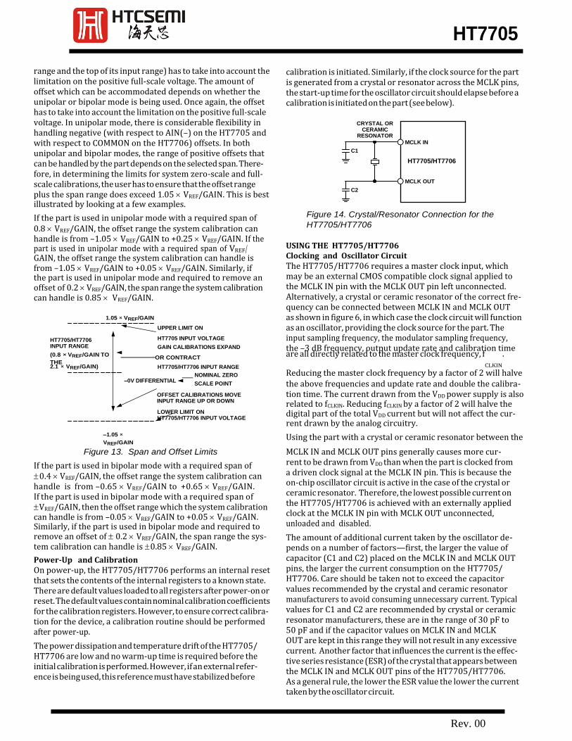
range and the top of its input range) has to take into account the limitation on the positive full-scale voltage. The amount of offset which can be accommodated depends on whether the unipolar or bipolar mode is being used. Once again, the offset has to take into account the limitation on the positive full-scale voltage. In unipolar mode, there is considerable flexibility in handling negative (with respect to AIN(–) on the HT7705 and with respect to COMMON on the HT7706) offsets. In both unipolar and bipolar modes, the range of positive offsets that can be handled by the part depends on the selected span. There- fore, in determining the limits for system zero-scale and full- scale calibrations, the user has to ensure that the offset range
calibration is initiated. Similarly, if the clock source for the part is generated from a crystal or resonator across the MCLK pins, the start-up time for the oscillator circuit should elapse before a calibration is initiated on the part (see below).
plus the span range does exceed 1.05 VREF/GAIN. This is best illustrated by looking at a few examples.
If the part is used in unipolar mode with a required span of 0.8 VREF/GAIN, the offset range the system calibration can handle is from –1.05 VREF/GAIN to +0.25 VREF/GAIN. If the part is used in unipolar mode with a required span of VREF/ GAIN, the offset range the system calibration can handle is from –1.05 VREF/GAIN to +0.05 VREF/GAIN. Similarly, if the part is used in unipolar mode and required to remove an offset of 0.2 VREF/GAIN, the span range the system calibration can handle is 0.85 VREF/GAIN.
1.05 × VREF/GAIN
UPPER LIMIT ON
Figure 14. Crystal/Resonator Connection for the
HT7705/HT7706
USING THE HT7705/HT7706 Clocking and Oscillator Circuit The HT7705/HT7706 requires a master clock input, which may be an external CMOS compatible clock signal applied to the MCLK IN pin with the MCLK OUT pin left unconnected. Alternatively, a crystal or ceramic resonator of the correct fre- quency can be connected between MCLK IN and MCLK OUT as shown in figure 6, in which case the clock circuit will function as an oscillator, providing the clock source for the part. The
HT7705/HT7706 INPUT RANGE
HT7705 INPUT VOLTAGE
GAIN CALIBRATIONS EXPAND
input sampling frequency, the modulator sampling frequency, the –3 dB frequency, output update rate and calibration time
(0.8 × VREF/GAIN TO OR CONTRACT
THE
are all directly related to the master clock frequency, f .
2.1 × VREF/GAIN) HT7705/HT7706 INPUT RANGE
NOMINAL ZERO
CLKIN
Reducing the master clock frequency by a factor of 2 will halve –0V DIFFERENTIAL
SCALE POINT the above frequencies and update rate and double the calibra-
–1.05 ×
VREF/GAIN
OFFSET CALIBRATIONS MOVE INPUT RANGE UP OR DOWN
LOWER LIMIT ON HT7705/HT7706 INPUT VOLTAGE
tion time. The current drawn from the VDD power supply is also related to fCLKIN. Reducing fCLKIN by a factor of 2 will halve the digital part of the total VDD current but will not affect the cur- rent drawn by the analog circuitry.
Using the part with a crystal or ceramic resonator between the
Figure 13. Span and Offset Limits
If the part is used in bipolar mode with a required span of 0.4 VREF/GAIN, the offset range the system calibration can handle is from –0.65 VREF/GAIN to +0.65 VREF/GAIN. If the part is used in bipolar mode with a required span of VREF/GAIN, then the offset range which the system calibration can handle is from –0.05 VREF/GAIN to +0.05 VREF/GAIN. Similarly, if the part is used in bipolar mode and required to remove an offset of 0.2 VREF/GAIN, the span range the sys- tem calibration can handle is 0.85 VREF/GAIN.
Power-Up and Calibration On power-up, the HT7705/HT7706 performs an internal reset that sets the contents of the internal registers to a known state. There are default values loaded to all registers after power-on or reset. The default values contain nominal calibration coefficients for the calibration registers. However, to ensure correct calibra- tion for the device, a calibration routine should be performed after power-up.
The power dissipation and temperature drift of the HT7705/ HT7706 are low and no warm-up time is required before the initial calibration is performed. However, if an external refer- ence is being used, this reference must have stabilized before
MCLK IN and MCLK OUT pins generally causes more cur- rent to be drawn from VDD than when the part is clocked from a driven clock signal at the MCLK IN pin. This is because the on-chip oscillator circuit is active in the case of the crystal or ceramic resonator. Therefore, the lowest possible current on the HT7705/HT7706 is achieved with an externally applied clock at the MCLK IN pin with MCLK OUT unconnected, unloaded and disabled.
The amount of additional current taken by the oscillator de- pends on a number of factors—first, the larger the value of capacitor (C1 and C2) placed on the MCLK IN and MCLK OUT pins, the larger the current consumption on the HT7705/ HT7706. Care should be taken not to exceed the capacitor values recommended by the crystal and ceramic resonator manufacturers to avoid consuming unnecessary current. Typical values for C1 and C2 are recommended by crystal or ceramic resonator manufacturers, these are in the range of 30 pF to 50 pF and if the capacitor values on MCLK IN and MCLK OUT are kept in this range they will not result in any excessive current. Another factor that influences the current is the effec- tive series resistance (ESR) of the crystal that appears between the MCLK IN and MCLK OUT pins of the HT7705/HT7706. As a general rule, the lower the ESR value the lower the current taken by the oscillator circuit.
CRYSTAL OR CERAMIC
RESONATOR
MCLK IN
C1
HT7705/HT7706
MCLK OUT
C2
HT7705
Rev. 00
When operating with a clock frequency of 2.4576 MHz, there is 50 A difference in the current between an externally applied clock and a crystal resonator when operating with a VDD of +3 V. With VDD = +5 V and fCLKIN = 2.4576 MHz, the typical current increases by 250 A for a crystal/resonator supplied clock versus an externally applied clock. The ESR values for crystals and resonators at this frequency tend to be low and as a result there tends to be little difference between different crystal and resonator types.
When operating with a clock frequency of 1 MHz, the ESR value for different crystal types varies significantly. As a result, the current drain varies across crystal types. When using a crys- tal with an ESR of 700 or when using a ceramic resonator, the increase in the typical current over an externally-applied clock is 20 A with VDD = +3 V and 200 A with VDD = +5 V. When using a crystal with an ESR of 3 k, the increase in the typical current over an externally applied clock is again 100 A with VDD = +3 V but 400 A with VDD = +5 V.
The on-chip oscillator circuit also has a start-up time associated with it before it is oscillating at its correct frequency and correct voltage levels. Typical start-up times with VDD = 5 V are 6 ms using a 4.9512 MHz crystal, 16 ms with a 2.4576 MHz crystal and 20 ms with a 1 MHz crystal oscillator. Start-up times are typically 20% slower when the power supply voltage is reduced to 3 V. At 3 V supplies, depending on the loading capacitances on the MCLK pins, a 1 M feedback resistor may be required across the crystal or resonator in order to keep the start up times around the 20 ms duration.
The HT7705/HT7706’s master clock appears on the MCLK OUT pin of the device. The maximum recommended load on this pin is one CMOS load. When using a crystal or ceramic resonator to generate the HT7705/HT7706’s clock, it may be desirable to use this clock as the clock source for the system. In this case, it is recommended that the MCLK OUT signal is buffered with a CMOS buffer before being applied to the rest of the circuit.
System Synchronization The FSYNC bit of the Setup Register allows the user to reset the modulator and digital filter without affecting any of the setup conditions on the part. This allows the user to start gath- ering samples of the analog input from a known point in time, i.e., when the FSYNC is changed from 1 to 0.
With a 1 in the FSYNC bit of the Setup Register, the digital filter and analog modulator are held in a known reset state and the part is not processing any input samples. When a 0 is then written to the FSYNC bit, the modulator and filter are taken out of this reset state and the part starts to gather samples again on the next master clock edge.
The FSYNC input can also be used as a software start convert command allowing the HT7705/HT7706 to be operated in a conventional converter fashion. In this mode, writing to the FSYNC bit starts conversion and the falling edge of DRDY
indicates when conversion is complete. The disadvantage of this scheme is that the settling time of the filter has to be taken into account for every data register update. This means that the rate at which the data register is updated is three times slower in this mode.
Since the FSYNC bit resets the digital filter, the full settling time of 3 1/Output Rate has to elapse before there is a new word loaded to the output register on the part. If the DRDY
signal is low when FSYNC goes to a 0, the DRDY signal will not be reset high by the FSYNC command. This is because the HT7705/HT7706 recognizes that there is a word in the data register which has not been read. The DRDY line will stay low until an update of the data register takes place, at which time it will go high for 500 tCLKIN before returning low again. A read from the data register resets the DRDY signal high and it will not return low until the settling time of the filter has elapsed (from the FSYNC command) and there is a valid new word in the data register. If the DRDY line is high when the FSYNC command is issued, the DRDY line will not return low until the settling time of the filter has elapsed.
Reset Input The RESET input on the HT7705/HT7706 resets all the logic, the digital filter and the analog modulator, while all on-chip registers are reset to their default state. DRDY is driven high and the HT7705/HT7706 ignores all communications to any of its registers while the RESET input is low. When the RESET
input returns high, the HT7705/HT7706 starts to process data and DRDY will return low in 3 1/Output Rate indicating a valid new word in the data register. However, the HT7705/ HT7706 operates with its default setup conditions after a RESET and it is generally necessary to set up all registers and carry out a calibration after a RESET command.
The HT7705/HT7706’s on-chip oscillator circuit continues to function even when the RESET input is low. The master clock signal continues to be available on the MCLK OUT pin. There- fore, in applications where the system clock is provided by the HT7705/HT7706’s clock, the HT7705/HT7706 produces an uninterrupted master clock during RESET commands.
Standby Mode The STBY bit in the Communications Register of the HT7705/ HT7706 allows the user to place the part in a power-down mode when it is not required to provide conversion results. The HT7705/HT7706 retains the contents of all its on-chip registers (including the data register) while in standby mode. When re- leased from standby mode, the part starts to process data and a new word is available in the data register in 3 1/Output rate from when a 0 is written to the STBY bit.
The STBY bit does not affect the digital interface, nor does it affect the status of the DRDY line. If DRDY is high when the STBY bit is brought low, it will remain high until there is a valid new word in the data register. If DRDY is low when the STBY bit is brought low, it will remain low until the data register is updated, at which time the DRDY line will return high for 500 tCLKIN before returning low again. If DRDY is low when the part enters its standby mode (indicating a valid unread word in the data register), the data register can be read while the part is in standby. At the end of this read operation, the DRDY will be reset high as normal.
HT7705
Rev. 00
Placing the part in standby mode reduces the total current to 9 A typical with VDD = 5 V and 4 A with VDD = 3 V when the part is operated from an external master clock provided this master clock is stopped. If the external clock continues to run in standby mode, the standby current increases to 150 A typical with 5 V supplies and 75 A typical with 3.3 V supplies. If a crystal or ceramic resonator is used as the clock source, the total current in standby mode is 400 A typical with 5 V supplies and 90 A with 3.3 V supplies. This is because the on-chip oscillator circuit continues to run when the part is in its standby mode. This is important in applications where the system clock is pro- vided by the HT7705/HT7706’s clock, so that the HT7705/ HT7706 produces an uninterrupted master clock even when it is in its standby mode.
Accuracy Sigma-Delta ADCs, like VFCs and other integrating ADCs, do not contain any source of nonmonotonicity and inherently offer no missing codes performance. The HT7705/HT7706 achieves excellent linearity by the use of high quality, on-chip capacitors, which have a very low capacitance/voltage coefficient. The de- vice also achieves low input drift through the use of chopper- stabilized techniques in its input stage. To ensure excellent performance over time and temperature, the HT7705/HT7706 uses digital calibration techniques that minimize offset and gain error.
Drift Considerations The HT7705/HT7706 uses chopper stabilization techniques to minimize input offset drift. Charge injection in the analog switches and dc leakage currents at the sampling node are the primary sources of offset voltage drift in the converter. The dc input leakage current is essentially independent of the selected gain. Gain drift within the converter depends primarily upon the temperature tracking of the internal capacitors. It is not affected by leakage currents.
Measurement errors due to offset drift or gain drift can be eliminated at any time by recalibrating the converter. Using
Supply Current The current consumption on the HT7705/HT7706 is specified for supplies in the range +2.7 V to +3.3 V and in the range +4.75 V to +5.25 V. The part operates over a +2.7 V to +5.25 V supply range and the IDD for the part varies as the supply voltage varies over this range. There is an internal current boost bit on the HT7705/HT7706 that is set internally in accordance with the operating conditions. This affects the current drawn by the analog circuitry within these devices. Minimum power consump- tion is achieved when the HT7705/HT7706 is operated with an fCLKIN of 1 MHz or at gains of 1 to 4 with fCLKIN = 2.4575 MHz as the internal boost bit is off reducing the analog current con- sumption. Figure 15 shows the variation of the typical IDD with VDD voltage for both a 1 MHz crystal oscillator and a 2.4576 MHz crystal oscillator at +25C. The HT7705/HT7706 is operated in unbuffered mode. The relationship shows that the IDD is mini- mized by operating the part with lower VDD voltages. IDD on the HT7705/HT7706 is also minimized by using an external master clock or by optimizing external components when using the on-chip oscillator circuit. Figures 3, 4, 6 and 7 show variations in IDD with gain, VDD and clock frequency using an external clock.
1600
1400
1200
1000
800
600
400
200
0
the system calibration mode can also minimize offset and gain errors in the signal conditioning circuitry. Integral and differen- tial linearity errors are not significantly affected by temperature
2.5 3.0 3.5 4.0 4.5 5.0
VDD
Figure 15. IDD vs. Supply Voltage
5.5
changes.
POWER SUPPLIES The HT7705/HT7706 operates with a VDD power supply be- tween 2.7 V and 5.25 V. While the latch-up performance of the HT7705/HT7706 is good, it is important that power is applied to the HT7705/HT7706 before signals at REF IN, AIN or the logic input pins in order to avoid excessive currents. If this is not possible, the current that flows in any of these pins should be limited. If separate supplies are used for the HT7705/HT7706 and the system digital circuitry, the HT7705/HT7706 should be powered up first. If it is not possible to guarantee this, current limiting resistors should be placed in series with the logic inputs to again limit the current. Latch-up current is greater than 100 mA.
Grounding and Layout Since the analog inputs and reference input are differential, most of the voltages in the analog modulator are common-mode volt- ages. The excellent common-mode rejection of the part will remove common-mode noise on these inputs. The digital filter will provide rejection of broadband noise on the power supplies, except at integer multiples of the modulator sampling frequency. The digital filter also removes noise from the analog and refer- ence inputs provided those noise sources do not saturate the analog modulator. As a result, the HT7705/HT7706 is more immune to noise interference than a conventional high resolu- tion converter. However, because the resolution of the HT7705/ HT7706 is so high, and the noise levels from the HT7705/ HT7706 so low, care must be taken with regard to grounding and layout.
fCLK = 1MHz
MCLK IN = CRYSTAL OSCILLATOR
TA = +25。C
UNBUFFERED MODE GAIN = 128
fCLK = 2.4576MHz
I DD
– µ
A
HT7705
Rev. 00
The printed circuit board that houses the HT7705 should be designed so that the analog and digital sections are separated and confined to certain areas of the board. This facilitates the use of ground planes which can be separated easily. A minimum etch technique is generally best for ground planes as it gives the best shielding. Digital and analog ground planes should only be joined in one place to avoid ground loops. If the HT7705/HT7706 is in a system where multiple devices require AGND-to-DGND connections, the connection should be made at one point only, a star ground point which should be established as close as possible to the HT7705 GND.
Avoid running digital lines under the device as these will couple noise onto the die. The analog ground plane should be allowed to run under the HT7705/HT7706 to avoid noise coupling. The power supply lines to the HT7705/HT7706 should use as large a trace as possible to provide low impedance paths and reduce the effects of glitches on the power supply line. Fast switching signals like clocks should be shielded with digital ground to avoid radiating noise to other sections of the board and clock signals should never be run near the analog inputs. Avoid cross- over of digital and analog signals. Traces on opposite sides of the board should run at right angles to each other. This will reduce the effects of feedthrough through the board. A micro- strip technique is by far the best, but is not always possible with a double-sided board. In this technique, the component side of the board is dedicated to ground planes while signals are placed on the solder side.
Good decoupling is important when using high resolution ADCs. All analog supplies should be decoupled with 10 F tantalum in parallel with 0.1 F ceramic capacitors to GND. To achieve the best from these decoupling components, they have to be placed as close as possible to the device, ideally right up against the device. All logic chips should be decoupled with 0.1 F disc ceramic capacitors to DGND.
Evaluating the HT7705/HT7706 Performance The recommended layout for the HT7705 and HT7706 is out- lined in their associated evaluation. These evaluation board packages include a fully assembled and tested evaluation board, documentation, software for controlling the board over the printer port of a PC and software for analyzing their perfor- mance on the PC.
Noise levels in the signals applied to the HT7705/HT7706 may also affect performance of the part. The HT7705/HT7706 soft- ware evaluation package allows the user to evaluate the true
performance of the part, independent of the analog input signal. The scheme involves using a test mode on the part where the inputs to the HT7705 are internally shorted together to provide a zero differential voltage for the analog modulator. External to the device, the AIN1(–) input on the HT7705 should be con- nected to a voltage that is within the allowable common-mode range of the part. Similarly, on the HT7706 the COMMON input should be connected to a voltage within its allowable common-mode range for evaluation purposes. This scheme should be used after a calibration has been performed on the part.
DIGITAL INTERFACE As previously outlined, the HT7705/HT7706’s programmable functions are controlled using a set of on-chip registers. Data is written to these registers via the part’s serial interface and read access to the on-chip registers is also provided by this interface. All communications to the part must start with a write operation to the Communications Register. After power-on or RESET, the device expects a write to its Communications Register. The data written to this register determines whether the next opera- tion to the part is a read or a write operation and also deter- mines to which register this read or write operation occurs. Therefore, write access to any of the other registers on the part starts with a write operation to the Communications Register followed by a write to the selected register. A read operation from any other register on the part (including the output data register) starts with a write operation to the Communications Register followed by a read operation from the selected register.
The HT7705/HT7706’s serial interface consists of five signals, CS, SCLK, DIN, DOUT and DRDY. The DIN line is used for transferring data into the on-chip registers while the DOUT line is used for accessing data from the on-chip registers. SCLK is the serial clock input for the device and all data transfers (either on DIN or DOUT) take place with respect to this SCLK signal. The DRDY line is used as a status signal to indicate when data is ready to be read from the HT7705/HT7706’s data register. DRDY goes low when a new data word is available in the out- put register. It is reset high when a read operation from the data register is complete. It also goes high prior to the updating of the output register to indicate when not to read from the device to ensure that a data read is not attempted while the register is being updated. CS is used to select the device. It can be used to decode the HT7705/HT7706 in systems where a number of parts are connected to the serial bus.
HT7705
Rev. 00
HT7705
Rev. 00
HT7705
Rev. 00
Figures 16 and 17 show timing diagrams for interfacing to the HT7705/HT7706 with CS used to decode the part. Figure 16 is for a read operation from the HT7705/HT7706’s output shift register while Figure 17 shows a write operation to the input shift register. It is possible to read the same data twice from the output register even though the DRDY line returns high after the first read operation. Care must be taken, however, to ensure that the read operations have been completed before the next output update is about to take place.
The HT7705/HT7706 serial interface can operate in three-wire mode by tying the CS input low. In this case, the SCLK, DIN and DOUT lines are used to communicate with the HT7705/ HT7706 and the status of DRDY can be obtained by interrogat- ing the MSB of the Communications Register. This scheme is suitable for interfacing to microcontrollers. If CS is required as a decoding signal, it can be generated from a port bit. For microcontroller interfaces, it is recommended that the SCLK idles high between data transfers.
The HT7705/HT7706 can also be operated with CS used as a frame synchronization signal. This scheme is suitable for DSP interfaces. In this case, the first bit (MSB) is effectively clocked out by CS since CS would normally occur after the falling edge of SCLK in DSPs. The SCLK can continue to run between data transfers provided the timing numbers are obeyed.
The serial interface can be reset by exercising the RESET input on the part. It can also be reset by writing a series of 1s on the DIN input. If a Logic 1 is written to the HT7705/HT7706 DIN line for at least 32 serial clock cycles the serial interface is reset. This ensures that in three-wire systems, if the interface gets lost either via a software error or by some glitch in the system, it can be reset back to a known state. This state returns the interface to where the HT7705/HT7706 is expecting a write operation to its Communications Register. This operation in itself does not reset the contents of any registers but since the interface was lost, the information written to any of the registers is unknown and it is advisable to set up all registers again.
Some microprocessor or microcontroller serial interfaces have a single serial data line. In this case, it is possible to connect the HT7705/HT7706’s DATA OUT and DATA IN lines together and connect them to the single data line of the processor. A 10 k pull-up resistor should be used on this single data line. In this case, if the interface gets lost, because the read and write operations share the same line the procedure to reset it back to a known state is somewhat different than previously described. It requires a read operation of 24 serial clocks followed by a write operation where a Logic 1 is written for at least 32 serial clock cycles to ensure that the serial interface is back into a known state.
DRDY
CS
SCLK
DOUT
Figure 16. Read Cycle Timing Diagram
CS
SCLK
DIN
Figure 17. Write Cycle Timing Diagram
t3
t10
t4 t6 t8
t5 t7 t9
MSB LSB
t11 t14 t16
t12 t 13
t15
MSB LSB
HT7705
Rev. 00
POLL DRDY PIN
WRITE TO COMMUNICATIONS REGISTER SETTING UP NEXT OPERATION TO BE A READ FROM THE DATA REGISTER (38 HEX)
POLL DRDY BIT OF COMMUNICATIONS REGISTER
READ FROM DATA REGISTER
WRITE TO COMMUNICATIONS REGISTER SETTING UP NEXT OPERATION TO BE A READ FROM THE DATA REGISTER (38 HEX)
READ FROM DATA REGISTER
NO DRDY LOW?
WRITE TO COMMUNICATIONS REGISTER SETTING UP NEXT OPERATION TO BE A READ FROM THE COMMUNICATIONS REGISTER (08 HEX)
YES
READ FROM COMMUNICATIONS REGISTER
NO DRDY LOW?
YES
WRITE TO CLOCK REGISTER SETTING THE CLOCK BITS IN ACCORDANCE WITH THE APPLIED MASTER CLOCK SIGNAL AND SELECT UPDATE RATE FOR
SELECTED CHANNEL (0C HEX)
WRITE TO COMMUNICATIONS REGISTER SELECTING CHANNEL & SETTING UP NEXT OPERATION TO BE A WRITE TO THE SETUP REGISTER (10 HEX)
START
POWER-ON/RESET FOR HT7705
CONFIGURE & INITIALIZE µC/µP SERIAL PORT
WRITE TO COMMUNICATIONS REGISTER SELECTING CHANNEL & SETTING UP NEXT OPERATION TO BE A WRITE TO THE CLOCK REGISTER (20 HEX)
CONFIGURING THE HT7705/HT7706 The HT7705/HT7706 contains six on-chip registers that the user can accesses via the serial interface. Communication with any of these registers is initiated by writing to the Communica- tions Register first. Figure 18 outlines a flow diagram of the sequence used to configure all registers after a power-up or reset on the HT7705, similar procedures apply to the HT7706. The flowchart also shows two different read options—the first where
the DRDY pin is polled to determine when an update of the data register has taken place, the second where the DRDY bit of the Communications Register is interrogated to see if a data register update has taken place. Also included in the flowing dia- gram is a series of words that should be written to the registers for a particular set of operating conditions. These conditions are gain of one, no filter sync, bipolar mode, buffer off, clock of 4.9512 MHz and an output rate of 50 Hz.
WRITE TO SETUP REGISTER CLEARING F SYNC, SETTING UP GAIN, OPERATING CONDITIONS & INITIATING A SELF-CALIBRATION ON SELECTED CHANNEL (40 HEX)
Figure 18. Flowchart for Setting Up and Reading from the HT7705
HT7705
Rev. 00
HT7705
Rev. 00
HT7705
Rev. 00
HT7705
Rev. 00

SS
68HC11
SCK
MISO
MOSI
VDD HT7705/HT7706
RESET
SCLK
DATA OUT
DATA IN
CS
MICROCOMPUTER/MICROPROCESSOR INTERFACING The HT7705/HT7706’s flexible serial interface allows for easy interface to most microcomputers and microprocessors. The flowchart of Figure 10 outlines the sequence that should be followed when interfacing a microcontroller or microprocessor to the HT7705/HT7706. Figures 19, 20 and 21 show some typical interface circuits.
The serial interface on the HT7705/HT7706 is capable of oper- ating from just three wires and is compatible with SPI interface protocols. The three-wire operation makes the part ideal for isolated systems where minimizing the number of interface lines minimizes the number of opto-isolators required in the system. The serial clock input is a Schmitt triggered input to accommo- date slow edges from opto-couplers. The rise and fall times of other digital inputs to the HT7705/HT7706 should be no longer than 1 s.
Most of the registers on the HT7705/HT7706 are 8-bit regis- ters, which facilitates easy interfacing to the 8-bit serial ports of microcontrollers. The Data Register on the HT7705/HT7706 is 16 bits, and the offset and gain registers are 24-bit registers but data transfers to these registers can consist of multiple 8-bit transfers to the serial port of the microcontroller. DSP proces- sors and microprocessors generally transfer 16 bits of data in a serial data operation. Some of these processors, such as the ADSP-2105, have the facility to program the amount of cycles in a serial transfer. This allows the user to tailor the number of bits in any transfer to match the register length of the required register in the HT7705/HT7706.
Even though some of the registers on the HT7705/HT7706 are only eight bits in length, communicating with two of these regis- ters in successive write operations can be handled as a single 16- bit data transfer if required. For example, if the Setup Register is to be updated, the processor must first write to the Communi- cations Register (saying that the next operation is a write to the Setup Register) and then write eight bits to the Setup Register. If required, this can all be done in a single 16-bit transfer be- cause once the eight serial clocks of the write operation to the Communications Register have been completed, the part imme- diately sets itself up for a write operation to the Setup Register.
HT7705/HT7706 to 68HC11 Interface Figure 19 shows an interface between the HT7705/HT7706 and the 68HC11 microcontroller. The diagram shows the minimum (three-wire) interface with CS on the HT7705/HT7706 hard- wired low. In this scheme, the DRDY bit of the Communica- tions Register is monitored to determine when the Data Register is updated. An alternative scheme, which increases the number of interface lines to four, is to monitor the DRDY output line from the HT7705/HT7706. The monitoring of the DRDY line can be done in two ways. First, DRDY can be connected to one of the 68HC11’s port bits (such as PC0), which is configured as an input. This port bit is then polled to determine the status of DRDY. The second scheme is to use an interrupt driven system, in which case the DRDY output is connected to the IRQ input of the 68HC11. For interfaces that require control of the CS
input on the HT7705/HT7706, one of the port bits of the 68HC11 (such as PC1), which is configured as an output, can be used to drive the CS input.
VDD
Figure 19. HT7705/HT7706 to 68HC11 Interface
The 68HC11 is configured in the master mode with its CPOL bit set to a logic one and its CPHA bit set to a logic one. When the 68HC11 is configured like this, its SCLK line idles high between data transfers. The HT7705/HT7706 is not capable of full duplex operation. If the HT7705/HT7706 is configured for a write operation, no data appears on the DATA OUT lines even when the SCLK input is active. Similarly, if the HT7705/ HT7706 is configured for a read operation, data presented to the part on the DATA IN line is ignored even when SCLK is active.
Coding for an interface between the 68HC11 and the HT7705/ HT7706 is given in Table XV. In this example, the DRDY
output line of the HT7705/HT7706 is connected to the PC0 port bit of the 68HC11 and is polled to determine its status.
Figure 20. HT7705/HT7706 to 8XC51 Interface
HT7705/HT7706 to 8051 Interface An interface circuit between the HT7705/HT7706 and the 8XC51 microcontroller is shown in Figure 20. The diagram shows the minimum number of interface connections with CS
on the HT7705/HT7706 hard-wired low. In the case of the 8XC51 interface the minimum number of interconnects is just two. In this scheme, the DRDY bit of the Communications Register is monitored to determine when the Data Register is updated. The alternative scheme, which increases the number of
VDD HT7705/HT7706
8XC51 VDD RESET
P3.0 DATA OUT
DATA IN
P3.1 SCLK
CS
HT7705
Rev. 00
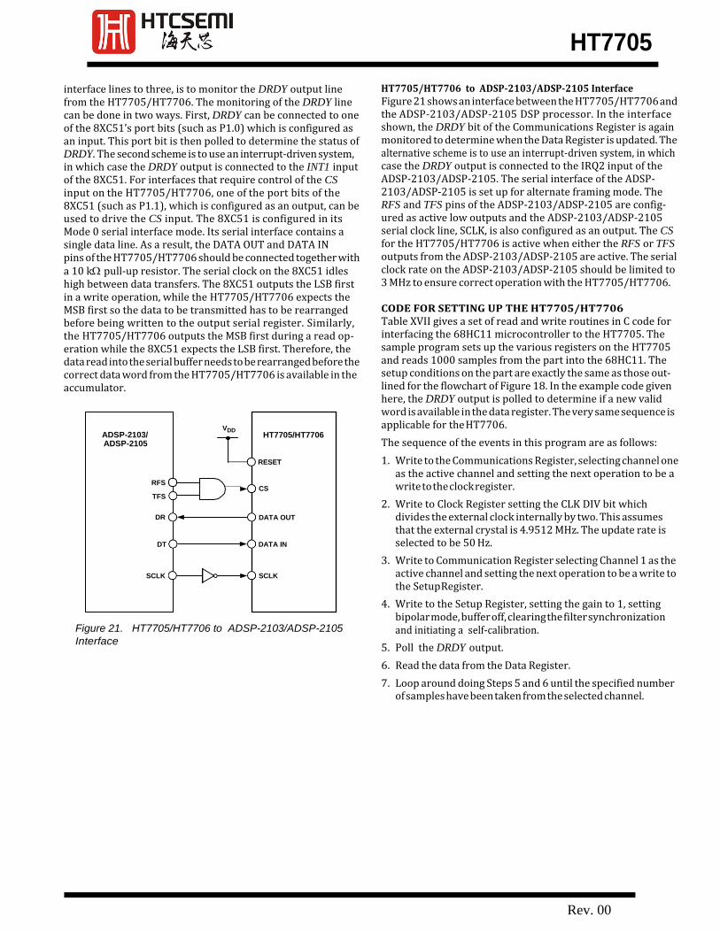
interface lines to three, is to monitor the DRDY output line from the HT7705/HT7706. The monitoring of the DRDY line can be done in two ways. First, DRDY can be connected to one of the 8XC51’s port bits (such as P1.0) which is configured as an input. This port bit is then polled to determine the status of DRDY. The second scheme is to use an interrupt-driven system, in which case the DRDY output is connected to the INT1 input of the 8XC51. For interfaces that require control of the CS
input on the HT7705/HT7706, one of the port bits of the 8XC51 (such as P1.1), which is configured as an output, can be used to drive the CS input. The 8XC51 is configured in its Mode 0 serial interface mode. Its serial interface contains a single data line. As a result, the DATA OUT and DATA IN pins of the HT7705/HT7706 should be connected together with a 10 k pull-up resistor. The serial clock on the 8XC51 idles high between data transfers. The 8XC51 outputs the LSB first in a write operation, while the HT7705/HT7706 expects the MSB first so the data to be transmitted has to be rearranged before being written to the output serial register. Similarly, the HT7705/HT7706 outputs the MSB first during a read op- eration while the 8XC51 expects the LSB first. Therefore, the data read into the serial buffer needs to be rearranged before the correct data word from the HT7705/HT7706 is available in the accumulator.
Figure 21. HT7705/HT7706 to ADSP-2103/ADSP-2105
Interface
HT7705/HT7706 to ADSP-2103/ADSP-2105 Interface Figure 21 shows an interface between the HT7705/HT7706 and the ADSP-2103/ADSP-2105 DSP processor. In the interface shown, the DRDY bit of the Communications Register is again monitored to determine when the Data Register is updated. The alternative scheme is to use an interrupt-driven system, in which case the DRDY output is connected to the IRQ2 input of the ADSP-2103/ADSP-2105. The serial interface of the ADSP- 2103/ADSP-2105 is set up for alternate framing mode. The RFS and TFS pins of the ADSP-2103/ADSP-2105 are config- ured as active low outputs and the ADSP-2103/ADSP-2105 serial clock line, SCLK, is also configured as an output. The CS
for the HT7705/HT7706 is active when either the RFS or TFS
outputs from the ADSP-2103/ADSP-2105 are active. The serial clock rate on the ADSP-2103/ADSP-2105 should be limited to 3 MHz to ensure correct operation with the HT7705/HT7706.
CODE FOR SETTING UP THE HT7705/HT7706 Table XVII gives a set of read and write routines in C code for interfacing the 68HC11 microcontroller to the HT7705. The sample program sets up the various registers on the HT7705 and reads 1000 samples from the part into the 68HC11. The setup conditions on the part are exactly the same as those out- lined for the flowchart of Figure 18. In the example code given here, the DRDY output is polled to determine if a new valid word is available in the data register. The very same sequence is applicable for the HT7706.
The sequence of the events in this program are as follows:
1. Write to the Communications Register, selecting channel one as the active channel and setting the next operation to be a write to the clock register.
2. Write to Clock Register setting the CLK DIV bit which divides the external clock internally by two. This assumes that the external crystal is 4.9512 MHz. The update rate is selected to be 50 Hz.
3. Write to Communication Register selecting Channel 1 as the active channel and setting the next operation to be a write to the Setup Register.
4. Write to the Setup Register, setting the gain to 1, setting bipolar mode, buffer off, clearing the filter synchronization and initiating a self-calibration.
5. Poll the DRDY output.
6. Read the data from the Data Register.
7. Loop around doing Steps 5 and 6 until the specified number of samples have been taken from the selected channel.
ADSP-2103/ ADSP-2105
VDD HT7705/HT7706
RESET
RFS
TFS
CS
DR DATA OUT
DT DATA IN
SCLK SCLK
HT7705
Rev. 00
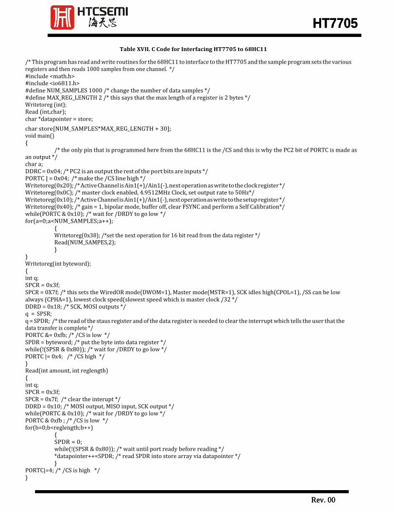
Table XVII. C Code for Interfacing HT7705 to 68HC11
/* This program has read and write routines for the 68HC11 to interface to the HT7705 and the sample program sets the various registers and then reads 1000 samples from one channel. */ #include <math.h> #include <io6811.h> #define NUM_SAMPLES 1000 /* change the number of data samples */ #define MAX_REG_LENGTH 2 /* this says that the max length of a register is 2 bytes */ Writetoreg (int); Read (int,char); char *datapointer = store;
char store[NUM_SAMPLES*MAX_REG_LENGTH + 30]; void main() {
/* the only pin that is programmed here from the 68HC11 is the /CS and this is why the PC2 bit of PORTC is made as an output */ char a; DDRC = 0x04; /* PC2 is an output the rest of the port bits are inputs */ PORTC | = 0x04; /* make the /CS line high */ Writetoreg(0x20); /* Active Channel is Ain1(+)/Ain1(-), next operation as write to the clock register */ Writetoreg(0x0C); /* master clock enabled, 4.9512MHz Clock, set output rate to 50Hz*/ Writetoreg(0x10); /* Active Channel is Ain1(+)/Ain1(-), next operation as write to the setup register */ Writetoreg(0x40); /* gain = 1, bipolar mode, buffer off, clear FSYNC and perform a Self Calibration*/ while(PORTC & 0x10); /* wait for /DRDY to go low */ for(a=0;a<NUM_SAMPLES;a++);
{ Writetoreg(0x38); /*set the next operation for 16 bit read from the data register */ Read(NUM_SAMPES,2); }
} Writetoreg(int byteword); { int q; SPCR = 0x3f; SPCR = 0X7f; /* this sets the WiredOR mode(DWOM=1), Master mode(MSTR=1), SCK idles high(CPOL=1), /SS can be low always (CPHA=1), lowest clock speed(slowest speed which is master clock /32 */ DDRD = 0x18; /* SCK, MOSI outputs */ q = SPSR; q = SPDR; /* the read of the staus register and of the data register is needed to clear the interrupt which tells the user that the data transfer is complete */ PORTC &= 0xfb; /* /CS is low */ SPDR = byteword; /* put the byte into data register */ while(!(SPSR & 0x80)); /* wait for /DRDY to go low */ PORTC |= 0x4; /* /CS high */ } Read(int amount, int reglength) { int q; SPCR = 0x3f; SPCR = 0x7f; /* clear the interupt */ DDRD = 0x10; /* MOSI output, MISO input, SCK output */ while(PORTC & 0x10); /* wait for /DRDY to go low */ PORTC & 0xfb ; /* /CS is low */ for(b=0;b<reglength;b++)
{ SPDR = 0; while(!(SPSR & 0x80)); /* wait until port ready before reading */ *datapointer++=SPDR; /* read SPDR into store array via datapointer */ }
PORTC|=4; /* /CS is high */ }
HT7705
Rev. 00
HT7705
Rev. 00
HT7705
Rev. 00
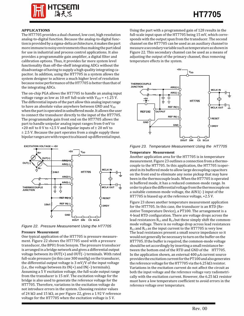
HT7705
AIN1(–)
24kfi
AIN2(+)
AIN2(–)
REF IN(–)
REF192
APPLICATIONS The HT7705 provides a dual channel, low cost, high resolution analog-to-digital function. Because the analog-to-digital func- tion is provided by a sigma-delta architecture, it makes the part more immune to noisy environments thus making the part ideal for use in industrial and process control applications. It also provides a programmable gain amplifier, a digital filter and calibration options. Thus, it provides far more system level functionality than off-the-shelf integrating ADCs without the disadvantage of having to supply a high quality integrating ca- pacitor. In addition, using the HT7705 in a system allows the system designer to achieve a much higher level of resolution because noise performance of the HT7705 is better than that of
Using the part with a programmed gain of 128 results in the full-scale input span of the HT7705 being 15 mV, which corre- sponds with the output span from the transducer. The second channel on the HT7705 can be used as an auxiliary channel to measure a secondary variable such as temperature as shown in Figure 22. This secondary channel can be used as a means of adjusting the output of the primary channel, thus removing temperature effects in the system.
+5V
VDD
THERMOCOUPLE
the integrating ADCs.
The on-chip PGA allows the HT7705 to handle an analog input voltage range as low as 10 mV full-scale with VREF = +1.25 V. The differential inputs of the part allow this analog input range to have an absolute value anywhere between GND and VDD
when the part is operated in unbuffered mode. It allows the user to connect the transducer directly to the input of the HT7705. The programmable gain front end on the HT7705 allows the part to handle unipolar analog input ranges from 0 mV to +20 mV to 0 V to +2.5 V and bipolar inputs of 20 mV to 2.5 V. Because the part operates from a single supply these bipolar ranges are with respect to a biased-up differential input.
JUNCTION
+5V
GND
OUTPUT
AIN1(+)
AIN1(–)
REF IN(+)
REF IN(–)
GND
HT7705
DOUT DIN CS SCLK
MCLK IN
MCLK OUT
RESET
DRDY
EXCITATION VOLTAGE = +5V
IN+
OUT(+)
OUT(–)
IN–
THERMOCOUPLE JUNCTION
15kfi
+5V
AIN1(+)
REF IN(+)
GND
VDD
MCLK IN
MCLK OUT
RESET
DRDY
Figure 23. Temperature Measurement Using the HT7705
Temperature Measurement Another application area for the HT7705 is in temperature measurement. Figure 23 outlines a connection from a thermo- couple to the HT7705. In this application, the HT7705 is oper- ated in its buffered mode to allow large decoupling capacitors on the front end to eliminate any noise pickup that may have been in the thermocouple leads. When the HT7705 is operated in buffered mode, it has a reduced common-mode range. In order to place the differential voltage from the thermocouple on a suitable common-mode voltage, the AIN1(–) input of the HT7705 is biased up at the reference voltage, +2.5 V.
Figure 23 shows another temperature measurement application for the HT7705. In this case, the transducer is an RTD (Re- sistive Temperature Device), a PT100. The arrangement is a 4-lead RTD configuration. There are voltage drops across the
DOUT DIN CS SCLK
Figure 22. Pressure Measurement Using the HT7705
Pressure Measurement One typical application of the HT7705 is pressure measure- ment. Figure 22 shows the HT7705 used with a pressure transducer, the BP01 from Sensym. The pressure transducer is arranged in a bridge network and gives a differential output voltage between its OUT(+) and OUT(–) terminals. With rated full-scale pressure (in this case 300 mmHg) on the transducer, the differential output voltage is 3 mV/V of the input voltage (i.e., the voltage between its IN(+) and IN(–) terminals). Assuming a 5 V excitation voltage, the full-scale output range from the transducer is 15 mV. The excitation voltage for the bridge is also used to generate the reference voltage for the HT7705. Therefore, variations in the excitation voltage do not introduce errors in the system. Choosing resistor values of 24 k and 15 k, as per Figure 22, gives a 1.92 V reference voltage for the HT7705 when the excitation voltage is 5 V.
lead resistances RL1 and RL4 but these simply shift the common- mode voltage. There is no voltage drop across lead resistances RL2 and RL3 as the input current to the HT7705 is very low.
The lead resistances present a small source impedance so it would not generally be necessary to turn on the buffer on the HT7705. If the buffer is required, the common-mode voltage should be set accordingly by inserting a small resistance be- tween the bottom end of the RTD and GND of the HT7705. In the application shown, an external 400 A current source provides the excitation current for the PT100 and also generates the reference voltage for the HT7705 via the 6.25 k resistor. Variations in the excitation current do not affect the circuit as both the input voltage and the reference voltage vary radiometri- cally with the excitation current. However, the 6.25 k resistor must have a low temperature coefficient to avoid errors in the reference voltage over temperature.
HT7705
Rev. 00
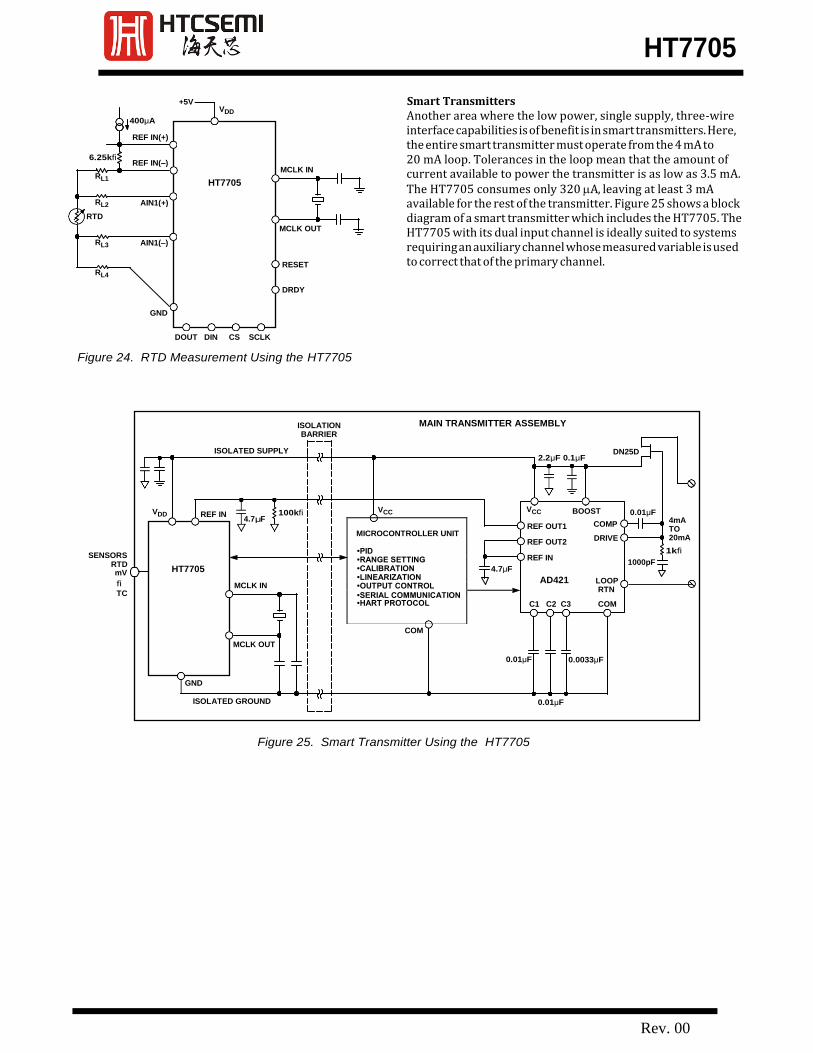
Smart Transmitters Another area where the low power, single supply, three-wire interface capabilities is of benefit is in smart transmitters. Here, the entire smart transmitter must operate from the 4 mA to 20 mA loop. Tolerances in the loop mean that the amount of current available to power the transmitter is as low as 3.5 mA. The HT7705 consumes only 320 A, leaving at least 3 mA available for the rest of the transmitter. Figure 25 shows a block diagram of a smart transmitter which includes the HT7705. The HT7705 with its dual input channel is ideally suited to systems requiring an auxiliary channel whose measured variable is used to correct that of the primary channel.
DOUT DIN CS SCLK
Figure 24. RTD Measurement Using the HT7705
SENSORS RTD mV
fi
TC
Figure 25. Smart Transmitter Using the HT7705
+5V VDD
400µA
REF IN(+)
6.25kfi REF IN(–)
RL1
MCLK IN
HT7705
RL2
RTD
AIN1(+)
MCLK OUT
RL3 AIN1(–)
RESET RL4
DRDY
GND
VCC
REF OUT1
REF OUT2
REF IN
BOOST
COMP
DRIVE
AD421
C1 C2 C3
LOOP RTN
COM
ISOLATION BARRIER
MAIN TRANSMITTER ASSEMBLY
ISOLATED SUPPLY 2.2µF 0.1µF
DN25D
VDD REF IN 4.7
VCC 0.01µF µ F
100kfi 4mA TO 20mA
1kfi
HT7705 1000pF
MCLK IN
COM
MCLK OUT
0.01µF 0.0033µF
GND
ISOLATED GROUND 0.01µF
MICROCONTROLLER UNIT
•PID •RANGE SETTING •CALIBRATION 4.7µF •LINEARIZATION •OUTPUT CONTROL •SERIAL COMMUNICATION •HART PROTOCOL
HT7705
Rev. 00
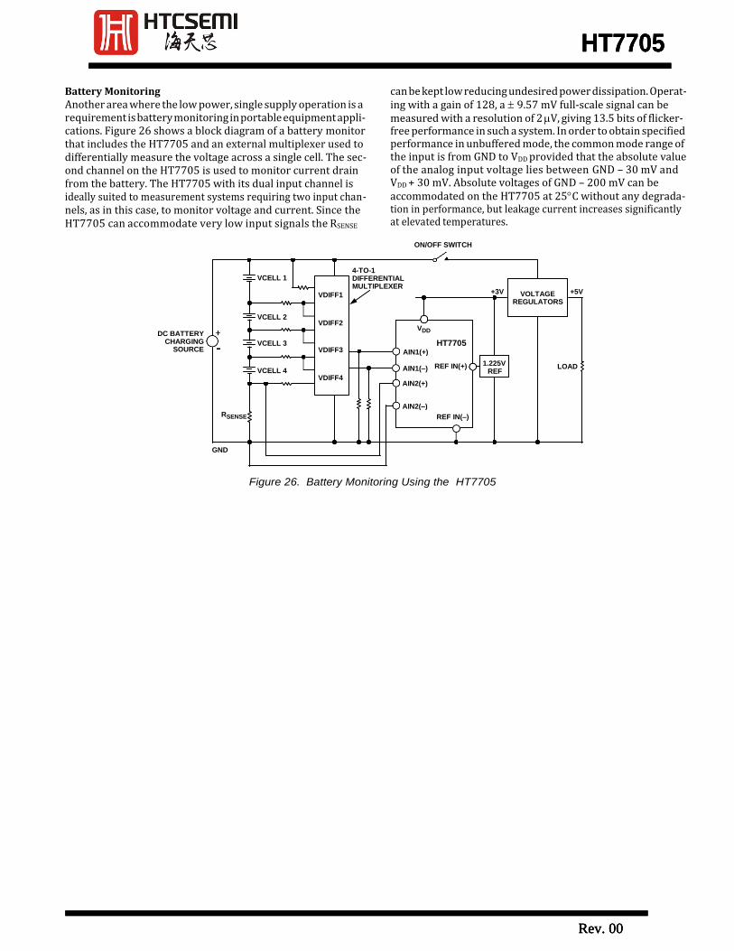
Battery Monitoring Another area where the low power, single supply operation is a requirement is battery monitoring in portable equipment appli- cations. Figure 26 shows a block diagram of a battery monitor that includes the HT7705 and an external multiplexer used to differentially measure the voltage across a single cell. The sec- ond channel on the HT7705 is used to monitor current drain from the battery. The HT7705 with its dual input channel is ideally suited to measurement systems requiring two input chan- nels, as in this case, to monitor voltage and current. Since the HT7705 can accommodate very low input signals the RSENSE
can be kept low reducing undesired power dissipation. Operat- ing with a gain of 128, a 9.57 mV full-scale signal can be measured with a resolution of 2 V, giving 13.5 bits of flicker- free performance in such a system. In order to obtain specified performance in unbuffered mode, the common mode range of the input is from GND to VDD provided that the absolute value of the analog input voltage lies between GND – 30 mV and VDD + 30 mV. Absolute voltages of GND – 200 mV can be accommodated on the HT7705 at 25C without any degrada- tion in performance, but leakage current increases significantly at elevated temperatures.
ON/OFF SWITCH
DC BATTERY
CHARGING SOURCE
Figure 26. Battery Monitoring Using the HT7705
VDIFF1
VDIFF2
VDIFF3
VDIFF4
VOLTAGE REGULATORS
VCELL 2
VDD
HT7705 AIN1(+)
AIN1(–)
AIN2(+)
REF IN(+)
AIN2(–)
REF IN(–)
LOAD
VCELL 4 1.225V
REF
VCELL 1 4-TO-1 DIFFERENTIAL MULTIPLEXER
+3V +5V
VCELL 3
RSENSE
GND
HT7705
Rev. 00
HT7705
Rev. 00
HT7705
Rev. 00
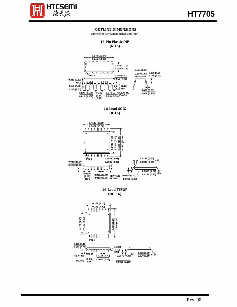
16 9
1 8
16 9
1 8
0.4133 (10.50)
0.3977 (10.00)
0.201 (5.10)
0.193 (4.90)
16 9
1 8
OUTLINE DIMENSIONS Dimensions shown in inches and (mm).
16-Pin Plastic DIP
(N-16)
0.840 (21.34)
0.745 (18.92)
0.280 (7.11)
0.240 (6.10)
0.325 (8.26)
0.300 (7.62) 0.195 (4.95) PIN 1 0.060 (1.52) 0.115 (2.93)
0.210 (5.33) 0.015 (0.38)
MAX 0.130
0.160 (4.06) (3.30)
0.115 (2.93) MIN 0.015 (0.381)
0.022 (0.558)
0.014 (0.356)
0.100
(2.54) BSC
0.070 (1.77) SEATING
0.045 (1.15) PLANE
0.008 (0.204)
16-Lead SOIC (R-16)
0.0118 (0.30)
PIN 1 0.1043 (2.65)
0.0926 (2.35)
0.0291 (0.74)
0.0098 (0.25) x 45。
0.0040 (0.10)
0.0500 (1.27) BSC
0.0192 (0.49)
SEATING
0.0138 (0.35) PLANE
8。
0.0125 (0.32) 0。
0.0091 (0.23)
0.0500 (1.27)
0.0157 (0.40)
16-Lead TSSOP (RU-16)
0.006 (0.15)
0.002 (0.05)
PIN 1
0.0433
(1.10) MAX
8° 0.028 (0.70) SEATING
0.0256 0.0118 (0.30)
0.0079 (0.20) 0°
0.020 (0.50)
PLANE (0.65) BSC
0.0075 (0.19) 0.0035 (0.090)
0.1
77
(4
.50)
0.1
69
(4
.30)
0.2
99
2 (
7.6
0)
0.2
91
4 (
7.4
0)
0.4
19
3 (
10
.65
)
0.3
93
7 (
10
.00
)
0.2
56
(6
.50)
0.2
46
(6
.25)
HT7705
Rev. 00