HIGHLY SECURE IMAGES STEGANOGRAPHY TECHNIQUES BASED ON LSB, X-BOX MAPPING AND HUFFMAN ENCODING

This article has been accepted for inclusion in a future issue of this journal. Content is final as presented, with the exception of pagination.
IEEE TRANSACTIONS ON VERY LARGE SCALE INTEGRATION (VLSI) SYSTEMS 1
Built-in Self-Calibration and Digital-Trim Techniquefor 14-Bit SAR ADCs Achieving ±1 LSB INL
Shankar Thirunakkarasu, Member, IEEE, and Bertan Bakkaloglu, Senior Member, IEEE
Abstract— Several state-of-the-art monitoring and controlsystems, such as dc motor controllers, power line monitoringand protection systems, instrumentation systems, and batterymonitors, require direct digitization of high-voltage (HV) inputsignals. Analog-to-digital converters (ADCs) that can digitizeHV signals require high linearity and low-voltage coefficientcapacitors. A built-in self-calibration and digital-trim algorithmcorrecting static mismatches in capacitive digital-to-analog con-verter (DAC) used in successive approximation register analog-to-digital converters (SAR ADCs) is proposed. The algorithm usesa dynamic error correction (DEC) capacitor to cancel the staticerrors occurring in each capacitor of the array as the first stepupon power-up and eliminates the need for an extra calibrationDAC. Self-trimming is performed digitally during normal ADCoperation. The algorithm is implemented on a 14-bit HV inputrange SAR ADC with integrated DEC capacitors. The IC isfabricated in 0.6-µm HV-compliant CMOS process, acceptingup to 24Vpp differential input signal. The proposed approachachieves 73.32-dB signal-to-noise and distortion ratio, which isan improvement of 12.03 dB after self-calibration at 400-kS/ssampling rate, consuming 90 mW from a ±15 V supply. Thecalibration circuitry occupies 28% of the capacitor DAC andconsumes <15 mW during operation. Measurement results showthat this algorithm reduces integral nonlinearity from as highas 7 LSBs down to 1 LSB, and it works even in the presenceof larger mismatches exceeding 260 LSBs. Similarly, it reducesdifferential nonlinearity errors from 10 LSBs down to 1 LSB.The ADC occupies an active area of 9.76 mm2.
Index Terms— Analog-to-digital (A/D) conversion, digitaltrimming, mismatch correction, self-calibration.
I. INTRODUCTION
SUCCESSIVE approximation register analog-to-digitalconverters (SAR ADCs) are used in medium-resolution
and medium-speed applications, such as motor control, batterymonitoring, touch-screen control, and other sensor interfaces,requiring low latency, monotonicity, and low quiescent powerconsumption [1]–[6]. A high-voltage (HV) input range oper-ation is enabled by directly sampling on the bottom plateof the capacitor array to achieve higher input impedance ata lower operating frequency specifically for industrial motorcontrol applications [7]. In conventional high-performance
Manuscript received November 15, 2013; revised February 28, 2014 andApril 15, 2014; accepted April 28, 2014. This work was supported by TexasInstruments.
S. Thirunakkarasu is with RF Mixed Signal Group, Broadcom Corporation,Austin, TX 78746 USA (e-mail: [email protected]).
B. Bakkaloglu is with Ira A. Fulton School of Engineering, Arizona StateUniversity, Tempe, AZ 85287-08406 USA (e-mail: [email protected]).
Color versions of one or more of the figures in this paper are availableonline at http://ieeexplore.ieee.org.
Digital Object Identifier 10.1109/TVLSI.2014.2321761
and high-resolution SAR converters, the fundamental bottle-neck in achieving lower integral and differential nonlinearity(INL/DNL) is the mismatches found between the binaryweighted capacitors in the capacitive DAC due to process mis-matches [5], [6]. The HV-SAR-ADCs enable direct connectionto HV inputs, minimizing the need for voltage scaling. How-ever, in HV-SAR-ADCs, apart from the mismatches betweenthe capacitors, linear and quadratic voltage coefficients ofcapacitors also dominate the INL. In addition, HV samplingswitches need to maintain constant impedance over the entireinput HV range in order to reduce distortion. Also, theseHV devices are prone to leakage and low speed with pro-nounced memory effect. Finally, it takes up a huge areato facilitate higher breakdown voltages, thereby increasingparasitics. Therefore, HV-SAR-ADCs typically achieve lowerlinearity performance than low-voltage SAR ADCs. In thispaper, a fully integrated self-calibration and digital trimmingalgorithm is proposed. The proposed approach does not requireany physical trim capacitors on the SAR ADC and performscalibration upon power-up.
The proposed all-digital self-trim algorithm is implementedon a 14-bit SAR ADC with integrated dynamic error correction(DEC) capacitors and the results were verified on a stand-alone SAR-ADC. This paper is organized as follows. Theconventional SAR-ADC calibration/trimming procedures arereviewed in Section II. Section III explains the architecture,algorithm, and implementation details of this paper. Theexperimental results are provided in Section IV, and finally,Section V draws the conclusion.
II. CONVENTIONAL SAR-ADC CALIBRATION/TRIMMING
Conventional built-in self-calibration procedures are car-ried out using extra physical trim capacitors, without usingdigital-only trimming [8]–[12], which takes additional diearea. In [13], each capacitor in the main array requires anindividual calibration capacitor, and calibration voltages aregenerated by resistive DACs, which again increases the area.Implementation in [14] involves extra switching sequences forcancelling the errors in the capacitors, reducing throughput.Another technique proposed in [15] collects 200 000 samplesusing two independent half-sized ADCs driving a least meansquare feedback loop in order to calibrate the capacitivedigital-to-analog converter (CDAC), thereby trying to achieveconvergence in the calibration algorithm. This takes a lot oftime in calibrating the mismatches. There are also a number ofother derived techniques [16]–[19] to calibrate the mismatches
1063-8210 © 2014 IEEE. Translations and content mining are permitted for academic research only. Personal use is also permitted,but republication/redistribution requires IEEE permission. See http://www.ieee.org/publications_standards/publications/rights/index.html for more information.

This article has been accepted for inclusion in a future issue of this journal. Content is final as presented, with the exception of pagination.
2 IEEE TRANSACTIONS ON VERY LARGE SCALE INTEGRATION (VLSI) SYSTEMS
Fig. 1. Self-calibration using memory and extra trim CDAC.
in the capacitors, which either occupy extra area or extratime. In this paper, an efficient self-calibration and digitaltrimming algorithm is proposed, which does not take any areafor implementing trim capacitors, does not reduce throughput,and takes almost negligible time in calibrating the mismatches.
An example of a traditional self-calibration and trim topol-ogy is shown in Fig. 1. Fig. 1 uses a memory for storingthe errors occurring in each capacitor of the main arrayand corrects it through an extra error correction trim CDACarray [8]. In the case of finding the mismatch of capacitor16C from the main array, a set of lower capacitors 8C, 4C,2C, and C are sampled to Vref while the top plate switch S0is grounded. This will store a known charge on the top platenode. Then, the bottom plate of capacitor 16C is tied to Vref ,while the top plate switch S0 is open, and other capacitors aregrounded. The exact point at which the comparator outputchanges sign is found by connecting bottom plates of thecapacitors in the trim-CDAC array one by one to Vref . Thisis the point at which the charge stored on the lower set ofcapacitors 8C, 4C, 2C, C, and C gets neutralized by thecharge stored on mismatched capacitor 16C together withthe trim-CDAC array, achieving binary relationship. Once theerror corresponding to capacitor 16C is stored in the memory,the errors of other higher capacitances 32C, 64C, and 128Care stored accordingly. After this calibration mode, duringnormal A/D conversion process, whenever the MSB capacitors16C, 32C, 64C, and 128C toggle from Gnd to Vref , the trimcapacitors associated with each of these capacitors, which arecalculated as described earlier, are also toggled from Gnd toVref using trim-CDAC array to maintain the binary relationshipbetween the capacitors. In this technique, the calibration andtrimming are performed using physical trim capacitors fromthe trim CDAC array.
In another traditional technique [11], [12], multiple trimcapacitors were used for each individual primary capacitor inthe array. In this approach, errors associated with each primarycapacitor are measured and calculated during the final test,and the error calibration codes are stored to program the trimcapacitors during normal operation.
III. PROPOSED SELF-CALIBRATION AND
DIGITAL-TRIM ALGORITHM
The algorithm is implemented with the help of DEC capac-itors explained in Section III-A. Section III-B introduces theactual self-calibration. A novel method to cancel out the chargeinjection-based offset error due to hold switch is explained inSection III-C. Section III-D introduces two different methodsof digital trimming algorithm.
A. Dynamic Error Correction
DEC helps in achieving redundancy during SAR ADCoperation. There are different techniques to achieve redun-dancy, as explained in [20]–[24]. Among them, [22]and [23] use nonbinary capacitor array implementation thatis not effective in a monolithic implementation with differentcapacitor dimensions, which is difficult to implement and willnot match properly. A general architecture for the proposed14-bit CDAC with DEC is shown in Fig. 2. There are two extracapacitors next to normal bit-6 capacitor, which are calledb6down-p and b6up-p on the P-side and b6down-n and b6up-n onthe N-side. These two capacitors on both P-side and N-side areemployed for differential DEC purposes, and it has the samevalue as normal bit-6 capacitor (256 LSBs). Similarly, thereare two extra capacitors next to normal bit-12 capacitor, whichare called b12down-p and b12up-p on the P-side and b12down-nand b12up-n on the N-side. These two capacitors on bothP-side and N-side are employed for differential DEC purpose,and it has the same value as normal bit-12 capacitor (4 LSBs).Similarly, there is one extra capacitor next to normal bit-14capacitor, which is called b14up. This capacitor on both P-sideand N-side is employed for single-ended DEC purpose, and ithas twice the value as normal bit-14 capacitor (2 LSBs).
The ideal values of the capacitors for a 14-bit converterconfiguration are shown below. Differential DEC at bit-6 andbit-12 and a single-ended DEC at bit-14 capacitor values areunderlined.
P-side caps = [8192 4096 2048 1024 512 256 256 256 12864 32 16 8 4 4 4 2 1 2 0.5 0.25 0.25].
N-side caps = [8192 4096 2048 1024 512 256 256 256 12864 32 16 8 4 4 4 2 1 2 0.5 0.25 0.25].
Fig. 2 exactly shows the position of switches during sam-pling phase. In the sampling phase, top plates of all thecapacitors in the MSB array on both CDACs are grounded.Bottom plates of certain capacitors on both P-side CDAC andN-side CDAC sample Vinp and Vinn, respectively. The numberof capacitors used for sampling is dependent on the followinggain equation stated in (1). This also decides the gain of theADC [25]. Typically, the inputs are sampled on
Csamp = Vref . CT
Vinp − Vinn(1)

This article has been accepted for inclusion in a future issue of this journal. Content is final as presented, with the exception of pagination.
THIRUNAKKARASU AND BAKKALOGLU: BUILT-IN SELF-CALIBRATION AND DIGITAL-TRIM TECHNIQUE 3
Fig. 2. Differential CDAC SAR A/D architecture utilizing the proposed self-calibration method in the sampling phase.
where Csamp is the total sampling capacitance and CT is thesum of all capacitances on either P-side or N-side.
In the case of differential error correction on bit-6 andbit-12, one of the error correction capacitors is sampling Gndand the other one is sampling Vref . As shown in Fig. 2,b6down-p and b6up-n sample Vref, and b6up-p and b6down-nsample Gnd, respectively. Similarly, in the bit-12 error correc-tion capacitors, b12down-p and b12up-n are sampling Vref andb12up-p and b12down-n are sampling Gnd, respectively. In thecase of single-ended error correction on bit-14, the bottomplate of this error correction capacitor 2 × b14up is samplingthe Gnd.
Once the input is sampled, the top plate of the capacitors inthe MSB array is disconnected from Gnd. The inputs are thendisconnected from the bottom plates, and a typical differentialSAR conversion process is performed. During conversion, themain aim is to achieve voltage convergence between Vcposand Vcneg, which are the two inputs of the comparator. Thedifference or the residue between Vcpos and Vcneg should beless than 1 LSB at the end of conversion to achieve a valid14-bit ADC output.
Also, during multiple clock cycles in a conversion phase,Vcpos and Vcneg could attain any voltage value dependingon the input voltage Vin equivalent to sampled Vinp–Vinn.At any given clock cycle of a conversion process, the maxi-mum difference between Vcpos and Vcneg should be less thanor equal to two times of its corresponding bit-test weight, i.e.,assume that at the end of sixth clock cycle in which bit-6capacitor is tested, the difference of voltages between Vcposand Vcneg should be less than or equal to two times b6 weightas stated in (2) as long as the input is within the specifiedrange
Vcpos − Vcneg < = 2 .b6
CT. Vref . (2)
This condition is checked using either differential or single-ended DEC capacitors, and it ensures that, at the end of
conversion process, Vcpos and Vcneg would converge to lessthan 1 LSB. If this condition is met, dynamic error does notoccur and all the MSB capacitors are completely settled duringthe conversion process. And if this condition is not met, itmeans that dynamic error exists and the MSB capacitors arenot settled. The DEC capacitors add or subtract voltages toVcpos and Vcneg to achieve convergence within 1 LSB. This islater accounted for digitally in a DEC process.
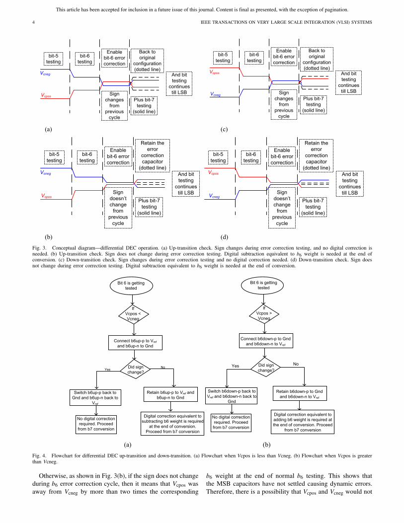
Figs. 3 and 4 explain the differential DEC in detail,specifically with respect to differential DEC capacitors placedbetween b6 and b7 capacitors above the scale-down capacitor.The same explanation is valid for operation of differentialDEC capacitors placed between b12 and b13 capacitors, and thesame concept is true for single-ended DEC capacitor placedafter b14. The value of the differential DEC capacitor is equalto that of the normal b6 capacitor. In Fig. 3(a), it is assumedthat Vcneg is greater than Vcpos during b5 testing. During b6testing, b6-p capacitor on the P-side is brought up from Gnd toVref , while the b5-n capacitor on the N-side is brought downfrom Vref to Gnd and b6-n capacitor is brought up from Gndto Vref . Equivalently, there is an addition of b6 weight on theP-side in Vcpos node while there is a subtraction of b6 weighton the N-side in Vcneg node.
Since Vcneg is greater than Vcpos during b6 testing, DECneeds to be performed by increasing the weight of Vcpos toanother b6 weight by switching the bottom plate of b6up-pon the P-side from Gnd to Vref and decreasing the weightof Vcneg to the same amount by switching the bottom plateof b6up-n from Vref to Gnd. If the signs change, then thismeans that Vcpos was closer to Vcneg by less than two timesthe corresponding b6 weight at the end of normal b6 testing.By ensuring this, Vcpos and Vcneg would converge to less than1 LSB at the end of conversion. In this case, the differentialDEC capacitors could be switched back to their originaldefault position before going ahead with b7 testing and soon, as shown in Fig. 3(a).
This article has been accepted for inclusion in a future issue of this journal. Content is final as presented, with the exception of pagination.
4 IEEE TRANSACTIONS ON VERY LARGE SCALE INTEGRATION (VLSI) SYSTEMS
Fig. 3. Conceptual diagram—differential DEC operation. (a) Up-transition check. Sign changes during error correction testing, and no digital correction isneeded. (b) Up-transition check. Sign does not change during error correction testing. Digital subtraction equivalent to b6 weight is needed at the end ofconversion. (c) Down-transition check. Sign changes during error correction testing and no digital correction needed. (d) Down-transition check. Sign doesnot change during error correction testing. Digital subtraction equivalent to b6 weight is needed at the end of conversion.
Fig. 4. Flowchart for differential DEC up-transition and down-transition. (a) Flowchart when Vcpos is less than Vcneg. (b) Flowchart when Vcpos is greaterthan Vcneg.
Otherwise, as shown in Fig. 3(b), if the sign does not changeduring b6 error correction cycle, then it means that Vcpos wasaway from Vcneg by more than two times the corresponding
b6 weight at the end of normal b6 testing. This shows thatthe MSB capacitors have not settled causing dynamic errors.Therefore, there is a possibility that Vcpos and Vcneg would not

This article has been accepted for inclusion in a future issue of this journal. Content is final as presented, with the exception of pagination.
THIRUNAKKARASU AND BAKKALOGLU: BUILT-IN SELF-CALIBRATION AND DIGITAL-TRIM TECHNIQUE 5
converge to less than 1 LSB at the end of SAR conversion.In this case, differential DEC capacitors are retained in thesame way as they were switched during error correctioncycle till the end of SAR conversion. The amount of chargeadded by the differential DEC capacitors in analog domainis equivalently subtracted in digital domain. This helps inachieving ease of convergence between Vcpos and Vcneg. Thisalso helps in bit cycling the SAR capacitors at the pretty fastrate achieving higher speed in high precision converters.
Fig. 4(a) shows a flowchart of the above mentioned proce-dure in the case of up-transition where the Vcpos is less thanVcneg during the start of b6 error correction cycle.
Similarly, Fig. 3(c) and (d) shows the node voltages of Vcposand Vcneg during b5, b6, and b6 error correction cycle for thecase in which Vcpos is greater than Vcneg at the end of b6testing. Therefore, we need to check dynamic errors for down-transition in this case. Also, Fig. 4(b) shows the flowchart ofthis procedure to check for DEC.
B. Built-in Self-Calibration Algorithm
The architecture for the proposed built-in self-calibrationalgorithm is shown in Fig. 2. In this segmented, differen-tial CDAC architecture, it is assumed that the first scale-down capacitor is placed between b6 and b7 capacitors andthe second scale-down capacitor is placed between b12 andb13 capacitors. The first and second scale-down capacitorsseparate the MSB array from the sub-MSB array and LSBarray, respectively. The scale-down capacitor provides thecapacitive division between the MSB array and sub-MSBarray. Because of this capacitive division, the scale-downcapacitor decreases the sensitivity of mismatch between thecapacitors in sub-MSB and LSB arrays. Therefore, only theMSB array is trimmed. Also, the variation in the parasiticcapacitor on the bottom plate of the first scale-down capacitorcauses an intrinsic mismatch between the MSB and the sub-MSB arrays. This mismatch needs to be corrected either bytrimming the first scale-down capacitor or equivalently eachof the MSB capacitors from b1 to b6. Trimming of the scale-down capacitor Cs1 may require laser trimming techniques ormore analog switches tied to the floating nodes, which leadsto extended test time, cost, and complexity. Also, trimmingb1–b6 individual capacitors can be achieved by additionalanalog circuits as discussed in Section II. In the proposedtechnique, a purely digital trimming approach completelyeliminating the trim capacitors, is followed without usinginput voltage Vin, where the errors in each capacitor fromb1 to b6 can be found using self-calibration technique. Theproposed method can correct for mismatches within an arrayand also between the P-side and N-side arrays in a fullydifferential CDAC since the errors will be found independentlyon both sides. In this built-in self-calibration approach, thecapacitor errors are found by first sampling b6down capacitor onthe P-side (b6down-p) to Vref and then performing differentialconversion from b7. The error of b6down-p is obtained bysubtracting the ideal expected value from this conversionresult. The error obtained on b6down-p will be half the valueof the original error because of the single-ended sampling
(P-side alone) on a single capacitor. In contrast to the tra-ditional easier techniques using physical trim capacitors inwhich single-ended sampling and single-ended conversion areperformed [8], [11] or differential sampling and differentialconversion are performed [8], [11], this technique eliminatesphysical trim capacitors and adopts the single-ended samplingindependently on both P-side and N-side with differentialconversion to account for the mismatches occurring in the bitcapacitances between the P-side and N-side arrays. In addition,this technique also corrects the mismatches found between thebinarily weighted capacitors within any array.
Similarly, the errors of b6up-p and b6-p capacitors are foundby sampling the respective capacitors followed by performingdifferential conversion from b7 and then subtracting from itsideal value. In the same way, the errors on b5-p, b4-p, . . . , b1-pcapacitors are also found by sampling each one of themseparately and then performing differential conversion fromb6, b5, . . . , b2, respectively, with dynamic correction employedat b6, b12, and b14 positions followed by subtraction from itsideal expected values.
The DEC is employed in [20] and [24] to reduce the settlingerrors during MSB cycles while the ADC is converting atfull speed. In the proposed architecture, the DEC is alsoemployed during self-calibration at bit positions b6, b12, andb14 while measuring the errors of b5, b4, . . . , b1 so thateven if each of these MSB capacitors are mismatched by alarge margin, up to the order of ±261 LSBs (b6 + b12 +b14), the error transfer function would still result in lessthan 1 LSB. In this way, the DEC capacitors are also usedfor calculating static mismatches in this algorithm. Using asimilar procedure, the errors are calculated on P-side andN-side capacitors independently. Let the errors of capac-itors b1-p, b2-p, . . . , b6-p, b6up-p, b6down-p, b1-n, b2-n, . . . , b6-n,b6up-n, and b6down-n obtained in this step be ε1-p, ε2-p, . . . ,ε6-p, ε6up-p, ε6down-p, ε1-n, ε2-n, . . . , ε6-n, ε6up−n, and ε6down-n.
The values of ε6-p, ε6up-p, ε6down-p, ε6-n, ε6up−n, andε6down-n obtained in the previous self-calibration step are notmodified. But, the errors associated with other capacitorsare modified depending on how the correction capacitors areused while doing conversion in the self-calibration phase. Themodifications that the capacitors on the P-side and N-side gothrough while calculating ε5-p to ε1-p, ε5-n to ε1-n is shownin Fig. 5. Fig. 5 is similar to Fig. 4(a) and (b) except that itis explained with context to self-calibration rather than pureDEC. For example, during self-calibration, while finding theerror associated with b5-p, after initially sampling b5-p aloneto Vref , Vcpos in Fig. 2 would be less than Vcneg. Therefore,DEC needs to be performed by switching b6up-p to Vref andb6up-n to Gnd, as shown in the flowchart in Fig. 5. The stepsin the flowchart should be exactly followed while calculatingε5-p. Similarly, the errors associated with b4-p, b3-p, . . . , b1-pare also calculated based on the flowchart shown in Fig. 5.In the same way, the errors associated with b5-n, b4-n, . . . , b1-nare also calculated. In the previous step, it could be seen thatthe errors calculated on the b5-p is correct only based on theassumption that b6 capacitors are all perfect. However, therecan be a mismatch on the b6 capacitors, which needs to beconsidered. Similarly, while calculating the errors associated

This article has been accepted for inclusion in a future issue of this journal. Content is final as presented, with the exception of pagination.
6 IEEE TRANSACTIONS ON VERY LARGE SCALE INTEGRATION (VLSI) SYSTEMS
Fig. 5. Differential DEC flowchart for up- and down-transition.
with b4-p, b3-p, . . . , b1-p, it is assumed that all the lowercapacitors are all accurate. But then in real scenario, the lowercapacitors would also be mismatched. In order to compensatefor this, a compensation factor needs to be added as follows.The final value of ε5-p is obtained by adding the previousε5-p with the ε6-p and ε6down-p as shown in (3) assuming thatb6down-p is always connected to Vref during sampling andalso during initial conversion till b6 capacitor
ε5-p(final) = ε5-p(previous) + ε6-p + ε6down-p. (3)
Similarly, final value of ε4-p is obtained by adding the previousε4-p with ε5-p, ε6−p, and ε6down−p, as shown in (4). The finalvalue of ε3-p to ε1-p is computed in the same manner
ε4-p(final) = ε4-p(previous) + ε5-p(previous) + ε6-p
+ε6down-p. (4)
For the case of ε5-n, its final value is computed by adding theprevious value of ε5-n with ε6-n and ε6up-n assuming b6up-nis initially connected to Vref during sampling, as shown inFig. 2, and also during initial conversion until differential DECtesting
ε5-n(final) = ε5-n(previous) + ε6-n + ε6up-n. (5)
The final value of ε4-n to ε1-n is found using the samemethod
ε4-n(final)=ε4-n(previous)+ε5-n(previous)+ε6-n+ε6up-n.(6)
By doing so, an estimate of the errors occurring on thecapacitors of both P- and N-side from b1 to b6 is known duringthis self-calibration step. Once the estimate of errors is knownfor each capacitor above the scale-down during self-calibrationstep, it is stored in local registers.
C. Charge Injection-Based Offset Error in Self-Calibration
During self-calibration, when each capacitor is individuallycalibrated from b6down-p, b6up-p, b6-p, . . . , b1-p on the P-side
and from b6down-n, . . . , b6up-n, b6-n, . . . , b1-n on the N-side,errors occur due to charge injection of the hold switch. Theamount of charge injection will be based on the impedancelooking into the top plate of the calibrating capacitor, whichis different for different calibrating capacitor. For example,as shown in Fig. 2, at the end of sampling phase in a self-calibration algorithm, when the hold switch opens, chargeinjection from the hold switch is different when b6down-pis sampled to Vref than when b1-p is sampled. This createsoffset error between different capacitors and may providefalse correction value during calibration. So, there shouldbe a charge injection-based offset cancellation that needsto be performed for different capacitors while it is beingcalibrated.
This is usually done after self-calibration algorithm iscompleted. To cancel the offset provided by the chargeinjection of the hold switch during b6down-p sampling phase,b6down-p is sampled to Vref on the bottom plate while thetop plate is grounded. In the hold phase, top plate holdswitch is opened, while the bottom of b6down-p is still con-nected to Vref . Next differential conversion is performedfrom b7 to calculate the offset due to charge injection ofhold switch during b6down-p calibration. Similarly, offset dueto charge injection of hold switch for different capacitorsis found independently and stored. These values are sub-tracted from the errors of different capacitors found in self-calibration algorithm to calculate the exact mismatches in eachcapacitor.
D. Digital Trimming
In the proposed digital-trimming process, during normalADC conversion process, whenever the MSB capacitors fromb1-p to b5-p is decided to be connected from Gnd to Vref onthe positive side, the sum of the respective errors computedfor those bits on both positive and negative sides need to beadded to the final digital output with mismatched physicalcapacitance. Also, whenever a b6 weight is subtracted, theε6down-p and ε6down-n are also subtracted. In the same way,whenever a b6 weight is added, the ε6up-p and ε6up-n arealso added. Implementing all the steps as stated earlier wouldensure that the final error plot to be within ±1 LSB.
Alternatively for digital trimming process, during normalADC conversion, it would also make sense to add the errorsfound on the positive side alone whenever the decision istaken for those MSB bits to be connected to Vref and theerrors found on the negative side could be subtracted when thecorresponding MSB capacitor on the positive side is decidedto be connected to Gnd. Both the options for digital trimmingprocess would function similarly and it could be provedmathematically as follows. Let the reference voltage used inthe circuit be Vref and let �Chigh,P denote the summation ofall capacitors tied high on the P-side at the end of conversion,�Chigh,N denotes the summation of capacitors tied high onthe N-side. If Ctotal,P and Ctotal,N denote the sum of allcapacitors tied both high and low, respectively, then (7) isvalid at the end of conversion. If we assume that �dNhigh,�dNlow, �dPhigh, and �dPlow denote the delta errors due to

This article has been accepted for inclusion in a future issue of this journal. Content is final as presented, with the exception of pagination.
THIRUNAKKARASU AND BAKKALOGLU: BUILT-IN SELF-CALIBRATION AND DIGITAL-TRIM TECHNIQUE 7
mismatches occurred on the capacitors of N-side tied high,low and on P-side tied high, low, respectively, at the end ofconversion, then (8) is valid
Vref · ∑Chigh,N
Ctotal,N= Vref · ∑ Chigh,P − Ctotal,P · Vin
Ctotal,P(7)
Vref .(∑
Chigh,N + ∑d Nhigh)
Ctotal,N
= Vref .(∑
Chigh,P +∑d Phigh)−Ctotal,P .Vin
Ctotal,P.
(8)
The relationship that describes the complementary nature of�Chigh,P and �Chigh,N is given by
∑Chigh,N
Ctotal,N= 1 −
∑Chigh,P
Ctotal,P. (9)
Since the two DACs are independent in terms of their actualcapacitor values, it is possible to write it in terms of ratios
∑Chigh
Ctotal= Code
FSCode(10)
where Code represents the equivalent digital output code forthe capacitors tied high and FSCode represents the full scaleoutput code. Also, since both DACs have the same resolution,FSCode is same for both and the compliment between thedigital equivalent of capacitors tied high on the positive sideCodeP and the one on the negative side CodeN is describedas
CodeN = FSCode − CodeP . (11)
Assuming that Dpcode,h and Dncode,h represents the summa-tion of digital equivalent of errors occurred in the capacitorstied high on the positive and negative side, respectively, then
Dncode,h
FSCode· Vref +
(
1 − CodeP
FSCode
)
· Vref
= Dpcode,h
FSCode· Vref − Vin + CodeP
FSCode.Vref (12)
Vin
Vref= 2.CodeP − Dncode,h + Dpcode,h
FSCode− 1 (13)
CodeP − Dncode,h
2+ Dpcode,h
2= FSCode
2+Vin. (14)
Here, if it is assumed that the input range is Vin orequivalently FSCode range from −Vref to +Vref , then FSCode/2indicates bipolar zero. Therefore, Vin is equal to the summationof decisions taken on the positive side minus the summationof half of the errors occurred in the capacitors tied high on thenegative side plus the summation of half of the errors occurredin the capacitors tied high on the positive side. Similarly, forthe alternative digital trimming procedure, reworking the abovederivation by substituting
Vref .∑
Chigh,N
Ctotal,N= Vref − Vref .
∑Clow,N
Ctotal,N(15)
Vref − Vref .(∑
Clow,N + ∑d Nlow)
Ctotal,N
= Vref .(∑
Chigh,P +∑d Phigh)−Ctotal,P . Vin
Ctotal,P. (16)
Fig. 6. Die micrograph.
Fig. 7. DNL before and after self-calibration.
Proceeding ahead in the same way as shown above for thefirst case, it will turn out to be
CodeP + Dncode,l
2+ Dpcode,h
2= FSCode
2+ Vin. (17)
In this case, Dncode,l denotes the summation of digitalequivalent of errors occurred in the capacitors tied low on thenegative side. Equation (17) states that during digital trimmingprocess, it is possible to add the sum of the errors foundon the positive and negative side of the MSB capacitors thatare decided to be connected to Vref on the P-side. This sumneed to be added with the intermediate digital output got withmismatched physical capacitances to get the final digital outputvalue. Equations (14) and (17) show different ways of doingdigital trimming process both of which are valid.
IV. MEASUREMENT RESULTS
The proposed on-chip, self-calibrated, and digitally trimmedHV compliant SAR ADC core occupies an area of 9.76 mm2.This area includes HV compliant bootstrapped input switches,internal reference, reference buffer, internal oscillator, fuses,

This article has been accepted for inclusion in a future issue of this journal. Content is final as presented, with the exception of pagination.
8 IEEE TRANSACTIONS ON VERY LARGE SCALE INTEGRATION (VLSI) SYSTEMS
Fig. 8. INL before and after self-calibration.
Fig. 9. FFT plot before self-calibration.
and digital logic. A die micrograph is shown in Fig. 6. ThisSAR-ADC consumes about 90 mW during normal operationfrom ±15 V supply. Input capacitance of 40 pF is used ineach CDAC and an internal reference of 4.096 V is used inthis design. The SAR uses a master clock of 20 MHz, and adifferential DEC is performed at bit-6 and bit-12 positionsusing 256- and 4-LSB capacitors, respectively. Moreover,single-ended DEC is also performed at bit-14 position using2-LSB capacitor. The density of the poly1-trinitride capacitorsused in CDAC array is 0.63 fF/μm2. The analog and digitalcircuitry for the proposed technique occupies less than 4% ofthe total area and consumes less than 3 mA during calibration.The proposed calibration technique has minimum impact onpower consumption during normal operation. Self-calibratingthe differential array takes just 515 μs on power-up, anddigital trimming process does not take any additional time.Fig. 7 compares the DNL before self-calibration and afterself-calibration. Similarly, Fig. 8 compares the INL. It wasseen that the INL errors in the order of 7 LSBs are reducedto less than 1 LSB after self-calibration at 14-bit level.
Fig. 10. FFT plot after self-calibration.
Fig. 11. SNDR and SFDR plot versus input frequency.
Figs. 9 and 10 compare the FFT plot of the samples collectedat the output of ADC before and after self-calibration. For thiscase, the ADC is converting an input sine wave of 5.053 kHzwhile running at a sampling rate of 400 kS/s. As shown inFig. 9, before self-calibration, the ADC has less than 65-dBtotal harmonic distortion (THD) due to capacitive mismatch.This THD improves by 24 dB after self-calibration is per-formed. The signal-to-noise and distortion ratio (SNDR) valuebefore self-calibration is 61.29 dB, and after self-calibration, itis 73.32 dB. Fig. 11 shows the SNDR and SFDR values acrossdifferent input frequencies. The DEC is used both duringnormal operation as well as during initial calibration. The DECimproves the INL performance of the order of 0.5 LSB at400 kS/s. While running at 500 kS/s, it makes a difference of1 LSB with and without DEC. The overhead being the threeextra clock cycles for each conversion, but the clocks now runfaster with DEC to compensate for it. Even after accountingfor three extra clocks for DEC, the effective conversion speedis much higher for the required INL performance. Table Itabulates the achieved performance with this implementation
This article has been accepted for inclusion in a future issue of this journal. Content is final as presented, with the exception of pagination.
THIRUNAKKARASU AND BAKKALOGLU: BUILT-IN SELF-CALIBRATION AND DIGITAL-TRIM TECHNIQUE 9
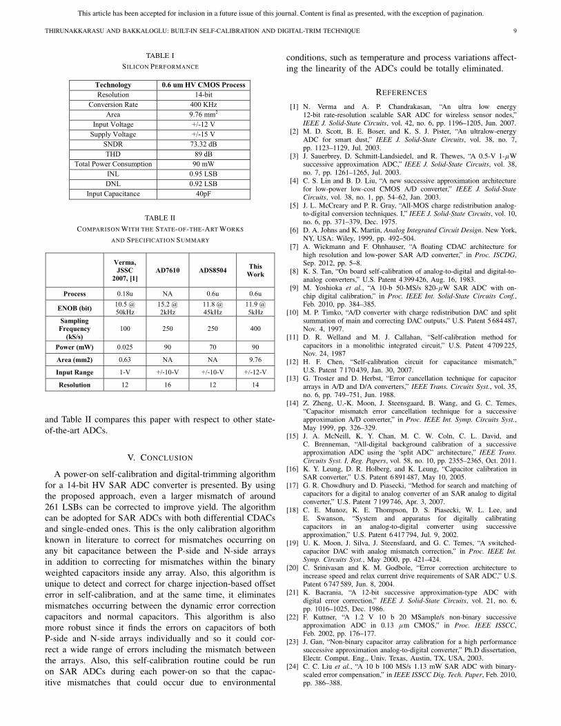
TABLE I
SILICON PERFORMANCE
TABLE II
COMPARISON WITH THE STATE-OF-THE-ART WORKS
AND SPECIFICATION SUMMARY
and Table II compares this paper with respect to other state-of-the-art ADCs.
V. CONCLUSION
A power-on self-calibration and digital-trimming algorithmfor a 14-bit HV SAR ADC converter is presented. By usingthe proposed approach, even a larger mismatch of around261 LSBs can be corrected to improve yield. The algorithmcan be adopted for SAR ADCs with both differential CDACsand single-ended ones. This is the only calibration algorithmknown in literature to correct for mismatches occurring onany bit capacitance between the P-side and N-side arraysin addition to correcting for mismatches within the binaryweighted capacitors inside any array. Also, this algorithm isunique to detect and correct for charge injection-based offseterror in self-calibration, and at the same time, it eliminatesmismatches occurring between the dynamic error correctioncapacitors and normal capacitors. This algorithm is alsomore robust since it finds the errors on capacitors of bothP-side and N-side arrays individually and so it could cor-rect a wide range of errors including the mismatch betweenthe arrays. Also, this self-calibration routine could be runon SAR ADCs during each power-on so that the capac-itive mismatches that could occur due to environmental
conditions, such as temperature and process variations affect-ing the linearity of the ADCs could be totally eliminated.
REFERENCES
[1] N. Verma and A. P. Chandrakasan, “An ultra low energy12-bit rate-resolution scalable SAR ADC for wireless sensor nodes,”IEEE J. Solid-State Circuits, vol. 42, no. 6, pp. 1196–1205, Jun. 2007.
[2] M. D. Scott, B. E. Boser, and K. S. J. Pister, “An ultralow-energyADC for smart dust,” IEEE J. Solid-State Circuits, vol. 38, no. 7,pp. 1123–1129, Jul. 2003.
[3] J. Sauerbrey, D. Schmitt-Landsiedel, and R. Thewes, “A 0.5-V 1-μWsuccessive approximation ADC,” IEEE J. Solid-State Circuits, vol. 38,no. 7, pp. 1261–1265, Jul. 2003.
[4] C. S. Lin and B. D. Liu, “A new successive approximation architecturefor low-power low-cost CMOS A/D converter,” IEEE J. Solid-StateCircuits, vol. 38, no. 1, pp. 54–62, Jan. 2003.
[5] J. L. McCreary and P. R. Gray, “All-MOS charge redistribution analog-to-digital conversion techniques. I,” IEEE J. Solid-State Circuits, vol. 10,no. 6, pp. 371–379, Dec. 1975.
[6] D. A. Johns and K. Martin, Analog Integrated Circuit Design. New York,NY, USA: Wiley, 1999, pp. 492–504.
[7] A. Wickmann and F. Ohnhauser, “A floating CDAC architecture forhigh resolution and low-power SAR A/D converter,” in Proc. ISCDG,Sep. 2012, pp. 5–8.
[8] K. S. Tan, “On board self-calibration of analog-to-digital and digital-to-analog converters,” U.S. Patent 4 399 426, Aug. 16, 1983.
[9] M. Yoshioka et al., “A 10-b 50-MS/s 820-μW SAR ADC with on-chip digital calibration,” in Proc. IEEE Int. Solid-State Circuits Conf.,Feb. 2010, pp. 384–385.
[10] M. P. Timko, “A/D converter with charge redistribution DAC and splitsummation of main and correcting DAC outputs,” U.S. Patent 5 684 487,Nov. 4, 1997.
[11] D. R. Welland and M. J. Callahan, “Self-calibration method forcapacitors in a monolithic integrated circuit,” U.S. Patent 4 709 225,Nov. 24, 1987
[12] H. F. Chen, “Self-calibration circuit for capacitance mismatch,”U.S. Patent 7 170 439, Jan. 30, 2007.
[13] G. Troster and D. Herbst, “Error cancellation technique for capacitorarrays in A/D and D/A converters,” IEEE Trans. Circuits Syst., vol. 35,no. 6, pp. 749–751, Jun. 1988.
[14] Z. Zheng, U.-K. Moon, J. Steensgaard, B. Wang, and G. C. Temes,“Capacitor mismatch error cancellation technique for a successiveapproximation A/D converter,” in Proc. IEEE Int. Symp. Circuits Syst.,May 1999, pp. 326–329.
[15] J. A. McNeill, K. Y. Chan, M. C. W. Coln, C. L. David, andC. Brenneman, “All-digital background calibration of a successiveapproximation ADC using the ‘split ADC’ architecture,” IEEE Trans.Circuits Syst. I, Reg. Papers, vol. 58, no. 10, pp. 2355–2365, Oct. 2011.
[16] K. Y. Leung, D. R. Holberg, and K. Leung, “Capacitor calibration inSAR converter,” U.S. Patent 6 891 487, May 10, 2005.
[17] G. R. Chowdhury and D. Piasecki, “Method for search and matching ofcapacitors for a digital to analog converter of an SAR analog to digitalconverter,” U.S. Patent 7 199 746, Apr. 3, 2007.
[18] C. E. Munoz, K. E. Thompson, D. S. Piasecki, W. L. Lee, andE. Swanson, “System and apparatus for digitally calibratingcapacitors in an analog-to-digital converter using successiveapproximation,” U.S. Patent 6 417 794, Jul. 9, 2002.
[19] U. K. Moon, J. Silva, J. Steensfaard, and G. C. Temes, “A switched-capacitor DAC with analog mismatch correction,” in Proc. IEEE Int.Symp. Circuits Syst., May 2000, pp. 421–424.
[20] C. Srinivasan and K. M. Godbole, “Error correction architecture toincrease speed and relax current drive requirements of SAR ADC,” U.S.Patent 6 747 589, Jun. 8, 2004.
[21] K. Bacrania, “A 12-bit successive approximation-type ADC withdigital error correction,” IEEE J. Solid-State Circuits, vol. 21, no. 6,pp. 1016–1025, Dec. 1986.
[22] F. Kuttner, “A 1.2 V 10 b 20 MSample/s non-binary successiveapproximation ADC in 0.13 μm CMOS,” in Proc. IEEE ISSCC,Feb. 2002, pp. 176–177.
[23] J. Gan, “Non-binary capacitor array calibration for a high performancesuccessive approximation analog-to-digital converter,” Ph.D dissertation,Electr. Comput. Eng., Univ. Texas, Austin, TX, USA, 2003.
[24] C. C. Liu et al., “A 10 b 100 MS/s 1.13 mW SAR ADC with binary-scaled error compensation,” in IEEE ISSCC Dig. Tech. Paper, Feb. 2010,pp. 386–388.

This article has been accepted for inclusion in a future issue of this journal. Content is final as presented, with the exception of pagination.
10 IEEE TRANSACTIONS ON VERY LARGE SCALE INTEGRATION (VLSI) SYSTEMS
[25] T. P. Kearney, “Programmable input range ADC,” U.S. Patent 6 940 445,Sep. 6, 2005.
[26] M. Mueck and M. C. W. Coln, “Differential input successiveapproximation analog to digital converter with common mode rejection,”U.S. Patent 7 432 844, Oct. 7, 2008.
Shankar Thirunakkarasu (M’09) received the B.E.degree in electronics and communication engineer-ing from the College of Engineering at Guindy, AnnaUniversity, Chennai, India, in 2002, and the M.S.degree in electrical engineering from Arizona StateUniversity, Tempe, AZ, USA, in 2008, where he iscurrently pursuing the Ph.D. degree.
He was a Design Intern at On-Semiconductor,Phoenix, in 2007. From 2008 to 2013, he waswith Nyquist Converter Group and the AdvancedDevelopment for Precision Data Converters Group
at Texas Instruments, Tucson, AZ, USA, where he was involved in designinghigh-resolution A/D converters. Since 2013, he has been with Broadcom,Austin, TX, USA, where he is involved in the design of communicationreceivers for satellite and TV applications. His current research interestsinclude high-performance and high-frequency analog/mixed signal circuitdesigns.
Bertan Bakkaloglu (M’94–SM’08) received thePh.D. degree from Oregon State University, Corval-lis, OR, USA, in 1995.
He joined the Mixed Signal Wireless DesignGroup at Texas Instruments Inc., Dallas, TX, USA,where he is involved in analog, RF, and mixed-signalfront ends for wireless and wireline communicationICs. He was involved in system-on-chip designs withintegrated battery management and analog basebandfunctionality as a Design Leader. In 2004, he joinedthe Department of Electrical Engineering at Arizona
State University, Tempe, AZ, USA, as an Associate Professor. His currentresearch interests include RF and PA supply regulators, RF synthesizers,biomedical and instrumentation circuits and systems, high-speed RF dataconverters, and RF built-in-self-test circuits for communication ICs.
Dr. Bakkaloglu has been a Technical Program Chair and Steering CommitteeMember of the IEEE RFIC Conference, and an Associate Editor of the IEEETRANSACTIONS ON CIRCUITS AND SYSTEMS and the IEEE TRANSACTIONS
ON MICROWAVE THEORY AND TECHNIQUES.
Copyright © 2022 FDOKUMEN