Design and simulation of a new reversible ALU in quantum ...
15
Page 1/15 Design and simulation of a new reversible ALU in quantum-dot cellular automata technology nemat azimi ( [email protected] ) Young Researchers and Elite Club https://orcid.org/0000-0003-1762-6715 Shahriar Mohammadi K N Toosi University of Technology Faculty of Mechanical Engineering Ahmad Khalatbari KN Toosi: KN Toosi University of Technology maryam moshtaghi K N Toosi University of Technology Faculty of Mechanical Engineering Research Article Keywords: reversible logic, Arithmetic Login Unit, Quantum Dot Cellular Automata, ANG, evaluation metrics Posted Date: May 3rd, 2022 DOI: https://doi.org/10.21203/rs.3.rs-1076918/v1 License: This work is licensed under a Creative Commons Attribution 4.0 International License. Read Full License
-
Upload
khangminh22 -
Category
Documents
-
view
0 -
download
0
Transcript of Design and simulation of a new reversible ALU in quantum ...

Page 1/15
Design and simulation of a new reversible ALU inquantum-dot cellular automata technologynemat azimi ( [email protected] )
Young Researchers and Elite Club https://orcid.org/0000-0003-1762-6715Shahriar Mohammadi
K N Toosi University of Technology Faculty of Mechanical EngineeringAhmad Khalatbari
KN Toosi: KN Toosi University of Technologymaryam moshtaghi
K N Toosi University of Technology Faculty of Mechanical Engineering
Research Article
Keywords: reversible logic, Arithmetic Login Unit, Quantum Dot Cellular Automata, ANG, evaluationmetrics
Posted Date: May 3rd, 2022
DOI: https://doi.org/10.21203/rs.3.rs-1076918/v1
License: This work is licensed under a Creative Commons Attribution 4.0 International License. Read Full License
Page 2/15
AbstractWith dimension reduction of technology towards nanometers scale, every day, energy consumptionbecomes more resistant to advances in computer science. It is felt that existing technologies, includingCMOS technology, are approaching the limits of their progress. Using Quantum Dot Cellular Automata(QCA), is one the most promising solutions to replace existing technologies. Duo to its nature, has verylow energy losses. On the other hand, for energy consumption reduction, it can be useful to designcircuits without loss of information or in a reversible manner. Arithmetic Logic Unit (ALU) is known as theprincipal part of processor systems. In this paper, we introduce a reversible ALU unit based on QCAtechnology using existing reversible logic gates and the proposed ANG gate. The proposed method issimulated using QCADesigner. The proposed structures are simulated using QCADesigner version 2.0.3.The reversible ALU unit in spite of 43% increasing in occupied area, has an improvement of 34% and 27%in cell counts and latency, respectively.
1. IntroductionIn 1965, Gordon Moore, the founder of Intel, stated that the number of transistors in a circuit doublesevery 18 months. This is known as Moore’s Law [1]. This law is still valid today and the number oftransistors increases every year, and the circuits become smaller and more complex. However, thisgrowing trend is expected to reach its saturation in the near future, and we will soon see a halt in thisdevelopment in computer chip technology. On the other hand, the loss in energy in modern technology isan important and fundamental issue today. Increasing the number of transistors per unit area, in additionto increasing the processing speed, will increase the power dissipation by a large amount, and theamount of heat generated by the power dissipation will be very signi�cant compared to the chip size.Therefore, it can be said that the two main obstacles in developing circuits with more powerfulprocessing and smaller sizes are power dissipation and limitations in reducing the size of transistors [2].Due to the use of new design concepts, Quantum dot cellular automata technology has signi�cantcompression capability and very low power, in order to exploit physical relationships and implementunique patterns with desirable features such as very high speed and frequency at the terahertz scale. Ithas the potential to build next-generation computers. These features make it impossible to ignore theemerging technologies, Quantum dot cellular automata technology is an emerging, but promisingtechnology to replace CMOS technology.
First introduced by Landauer in 1961, the relationship between physical and logical reversibility, statesthat if the relationship between each input and output is not unique in any logic circuit, then it is logicallyirreversible and will waste energy.
According to the second law of thermodynamics, due to the processing of an irreversible logicaloperation, the amount of energy is lost that is exactly equal to KTLn2 per bit. K is Boltzmann constantT=300K ,K=1.3806505 ×10⁻²³ JK−1 [3]. Therefore, if a logical operation is irreversible, no matter whichtechnology is used in its design and implementation, it will de�nitely have power loss. In this study, a

Page 3/15
QCA-based reversible ALU structure by using the proposed ANG gate is designed and simulated. Theproposed ALU circuit is capable of performing logical and arithmetic operations such as Addition, AND,OR, and XOR. The simulation results in QCA Designer show that the proposed structure, compared toprevious designs, has improvement in terms of area, number of cells, and latency. The rest of this paper isorganized as follows: In Section 2, we review the background of QCA. Section 3, provides an overview ofprevious and related works. In Section 4, the proposed method is discussed and reported. Section 5reports the simulation of the proposed method and its results. Finally, Section 6, presents conclusionsand future works.
2. Related WorksSen et al. [4] proposed a reversible ALU unit with testability using a reversible multiplexer. The proposedALU unit has two parts: Reversible Arithmetic Unit (RLU), and Reversible Logic Unit (RLU). These Parts areintroduced separately, but the QCA structure of the proposed ALU are not presented. This design isimplemented using single-layer and circular cells which includes 9 �xed inputs and 15 additional outputs.This design is capable of 17 arithmetic and logic operations. Narsh et al. [5] proposed a design by usingHNG reversible gate which is capable of 7 arithmetic and 8 logical operations. In this design the authorsare focused on improvements in design parameters such as quantum cost, number of �xed inputs,additional outputs, reversible gates, and latency. Gosumi et al. [6], offered a 3-layer ALU structure by using4 Testable Full Adder gates. Their proposed design consists of 1069 cells, area of 2.34μm2, and latencyof 2 clocks. The main shortcoming of this design is large occupied area. Qadim et al. [7], presented asingle-bit ALU with AND, OR, XOR, and Full-Adder using QCA technology. The proposed design has 3layers, 464 cells, occupied area of 0.78μm2, and 3 clocks latency. This design is irreversible. In [8],authors proposed an ALU which performs 16 arithmetic and logic operations on pair vectors with 4 bits.This design includes 35596 cells, area of 11.37μm2 and 9 clocks latency. Irreversibility, lack of faulttolerance, large occupied area are the main shortcomings of this approach. Naghibzadeh et al. [9],proposed a reversible ALU design using a new reversible gate named HNG. Although this approach couldreduce cost and size in relation to similar gate, but it has high circuit complexity. This design consists of670 cells, occupied area of 0.921μm2 and 4 clocks latency. The design is capable of performing 16logic and arithmetic operations as well as one �xed input and two additional outputs. Oskouie andGhafari [10], offered an ALU unit using reversible gate named Double Feynman, and an AND gate, an ORgate, and a Full-Adder gate. Then, the output is selected by a multiplexer. The design is just capable of 4AND, OR, XOR, and ADD operations, and is implemented by using 3 layers. In [11], the authors introduceda reversible ALU which consists of a 4x4 reversible block named BS1 Block, a 3x3 reversible Fredkin gate,and two 3x3 Feynman gate. The proposed design has 375 cells and area of 0.53 um2. In [12], authorsproposed an ALU with QCA technology. The main advantages of the proposed method are lowcomplexity, high performance, low cell consumption, high speed, and small occupied area. The proposedstructure is designed in 3 levels and 4 gates: AND, OR, XOR, and Full Adder. This approach is implementedin 3 layers and includes 332 cells, area of 0.48μm2, and 3 clocks latency. Norouzi et al. proposed areversible ALU using reversible Fredkin and HNG gates based on QCA technology. This design includes 3

Page 4/15
Fredkin gates, and one HNG gate. The proposed design has one �xed input, and generates just oneadditional output. This circuit can perform 20 arithmetic and logic operations. The simulation of thisdesign has been done with 480 cells, and area of 0.75 μm2.
3. The Qca PrincipleIn this section, some of the basic concepts of QCA technology including logical gates, interconnection,and timing (as a way of synchronizing two devices) are presented.
A QCA cell, is a square structure, including 4 quantum point in four corners, and two electrons which areallowed to move between points. Due to Coulomb’s repulsion, electrons occupy diagonal points oppositeeach other. This feature results in two stable points and possible con�gurations are shown as cellularpolarization P = −1 for (“0”) and P = +1 for (“1”). Figure 1 shows a QCA cell and two possiblepolarizations [14].
Two basic structures in QCA are inverter and majority gate. By placing QCA cells laterally, a standard QCAwire can be made [15]. Diagram 2(a) shows a QCA based wire which is designed based on 90 or 45degrees. Figure 2(b) shows that �rst inverter splits input into two paths, and combine them to produceopposite polarization [14]. Also, Figure 2(b) shows that second inverter can create opposite polarizationby placing a cell diagonally in output path.
In plain QCA designs, 3-input and 5-input gates have important role in main architecture of circuit [17].The 3-input majority gate is a key logic gate in QCA based design, that calculate Boolean expression.Diagram 3 shows a 3-input majority gate, in which output of M as considered as logical function ofEquation (1) [18]. Also, OR, AND gates with 2 inputs are made by keeping constant one of inputs ofmajority gate for +1 and -1, respectively.
M (A B C) = AB + BC + AC (1)
The intersection point of wires or wire crossing is an important matter in design of QCA circuit. Threecrossing or intersection methods are proposed so far:
Single-layer Crossing: This type of QCA crossing is performed in one layer using QCA cells with 45and 90 degrees, each one is dedicated towards a bus or crossing point.
These different cells can pass across bus without having signi�cant effect on each other.
Multi-layer Crossing: Despite of previous method, multi-layer crossing use just 45- or 90-degree cells.A wire from bus connects to another layer; and after crossing across bus or intersection point, thewire returns to original layer.
Logical Crossing: Although this bus runs on a single layer, it just needs one type of QCA cell. Theeffects of wires of one bus on each other are neutralized by using different phases in each wire.
Page 5/15
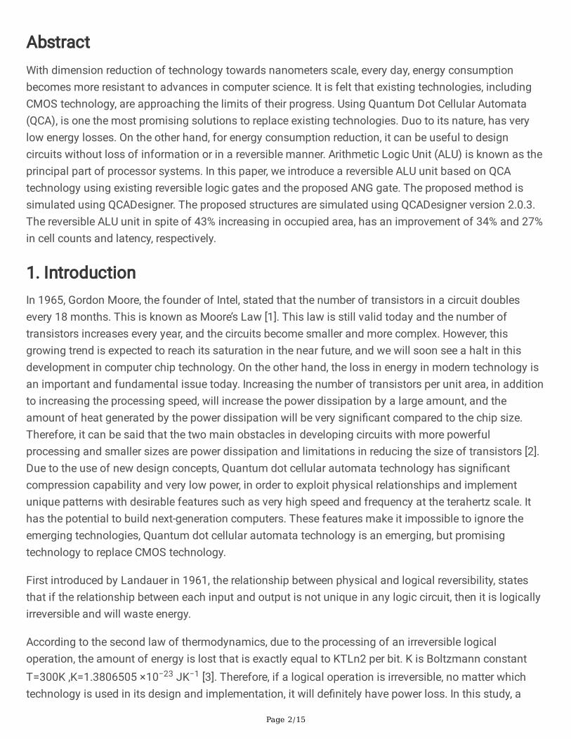
Cells with switch and hold phases are allowed to pass through cells with release and relax phases,respectively [19].
Clocking in QCA
Clocking is used in QCA-based circuits to increase controllability. In base state, arithmetic operations inQCA are performed by using one dimensional clock and in four phases. As it is shown in Figure 5, thereare 4 clocking zone in every QCA circuit, which are de�ned as four phases: Switch, Hold, Release, andRelax, each of these four phases is 90 degrees different from each other. In Switch phase, the energyboundaries within the point gradually increase and electrons at points can be affected by adjacent cellsthat are in the same phase as Switch or Hold. In Hold phase, due to increasing in energy boundaries, theelectrons can not be affected by adjacent cells. In Release phase, repulsing forces between points arereduced and the electrons are released gradually. In Relax phase, the cell has no polarity and the electronscan move freely within the cell [20].
4. The Proposed Reversible AluArithmetic and Logic Unit is in fact the processing core of any digital processor, which plays an importantand essential role in all stages of running a computer program. In ALUs designed based on irreversiblelogic, a large amount of power is consumed due to the loss of data bits. It is completely inevitable toavoid wasting such power in such designs. In order to improvement the performance of powerconsumption, it is necessary to design ALU in reversible manner. In this section, the proposed reversiblegate (ANG), proposed reversible ALU design, arithmetic and logic operation table that can be performedby the proposed plan, simulation of gate, and proposed design are discussed.
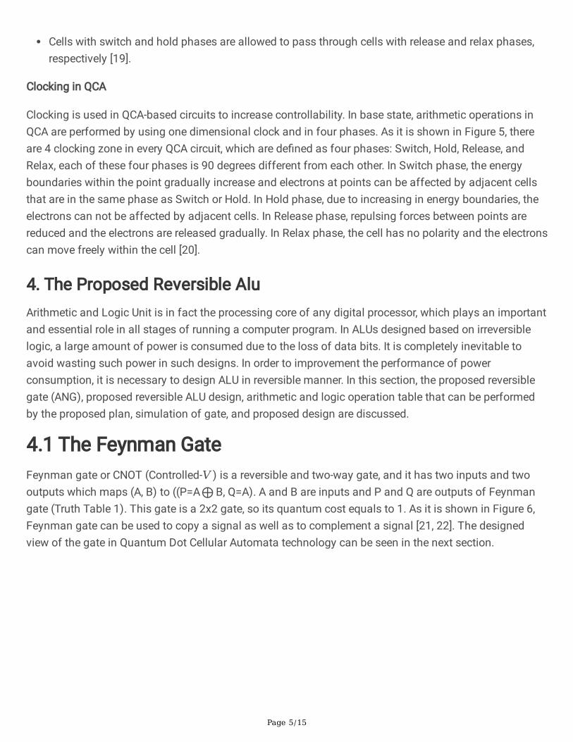
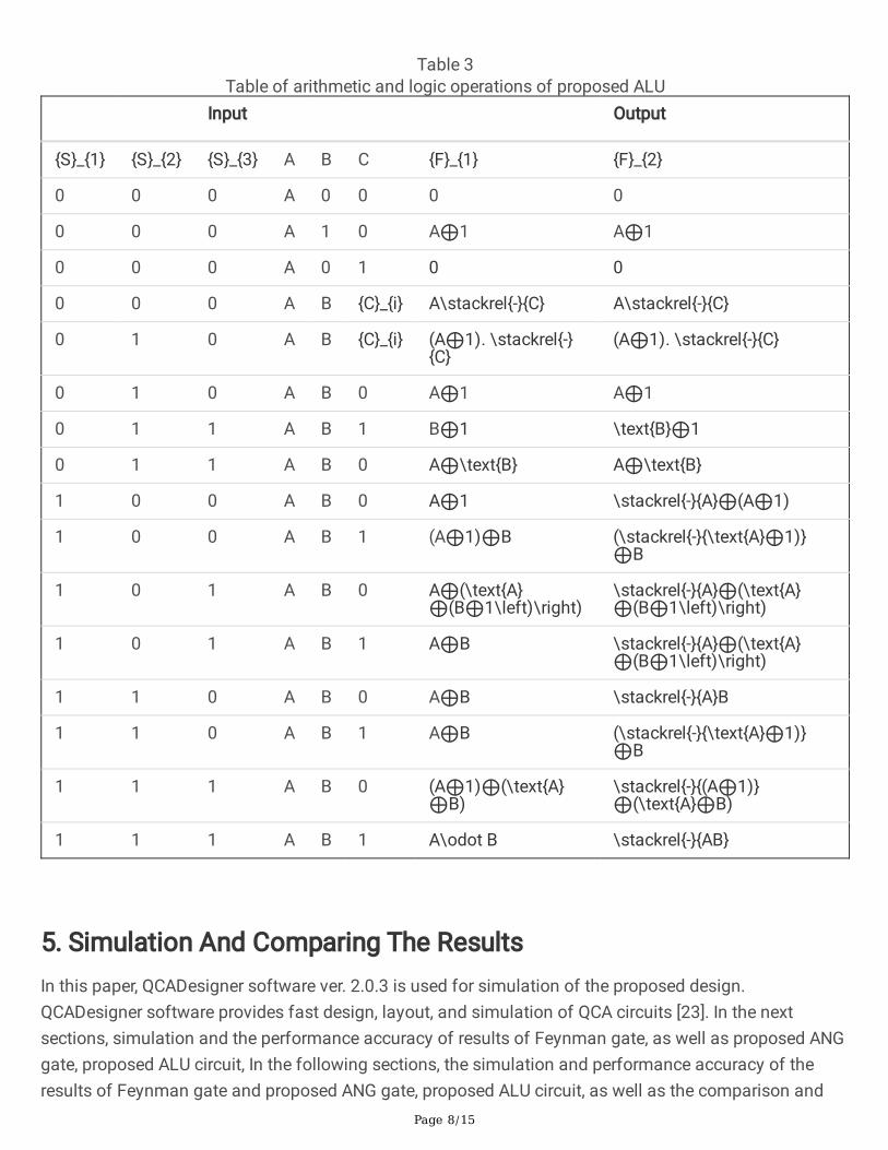
4.1 The Feynman GateFeynman gate or CNOT (Controlled-𝑉) is a reversible and two-way gate, and it has two inputs and twooutputs which maps (A, B) to ((P=A⨁ B, Q=A). A and B are inputs and P and Q are outputs of Feynmangate (Truth Table 1). This gate is a 2x2 gate, so its quantum cost equals to 1. As it is shown in Figure 6,Feynman gate can be used to copy a signal as well as to complement a signal [21, 22]. The designedview of the gate in Quantum Dot Cellular Automata technology can be seen in the next section.
Page 6/15
Table 1Table Truth for Feynman
gateInput Output
A B P Q
0 0 0 0
0 1 0 1
1 0 1 1
1 1 1 0
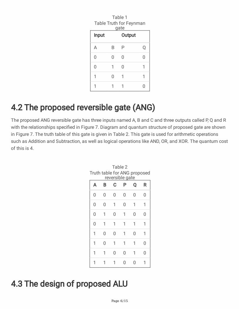
4.2 The proposed reversible gate (ANG)The proposed ANG reversible gate has three inputs named A, B and C and three outputs called P, Q and Rwith the relationships speci�ed in Figure 7. Diagram and quantum structure of proposed gate are shownin Figure 7. The truth table of this gate is given in Table 2. This gate is used for arithmetic operationssuch as Addition and Subtraction, as well as logical operations like AND, OR, and XOR. The quantum costof this is 4.
Table 2
Truth table for ANG proposedreversible gate
A B C P Q R
0 0 0 0 0 0
0 0 1 0 1 1
0 1 0 1 0 0
0 1 1 1 1 1
1 0 0 1 0 1
1 0 1 1 1 0
1 1 0 0 1 0
1 1 1 0 0 1
4.3 The design of proposed ALU
Page 7/15
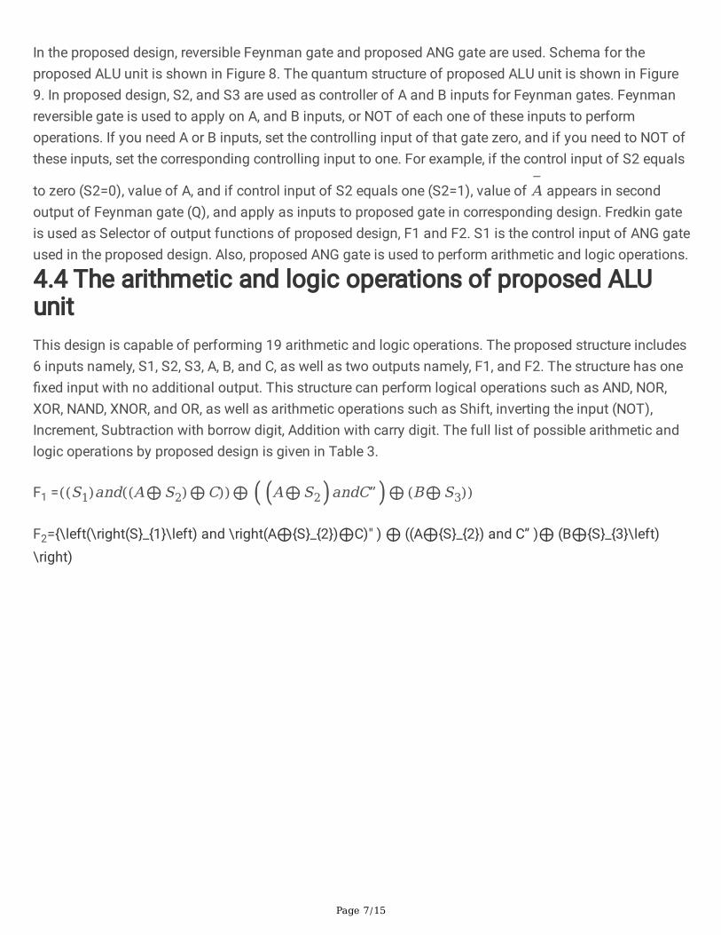
In the proposed design, reversible Feynman gate and proposed ANG gate are used. Schema for theproposed ALU unit is shown in Figure 8. The quantum structure of proposed ALU unit is shown in Figure9. In proposed design, S2, and S3 are used as controller of A and B inputs for Feynman gates. Feynmanreversible gate is used to apply on A, and B inputs, or NOT of each one of these inputs to performoperations. If you need A or B inputs, set the controlling input of that gate zero, and if you need to NOT ofthese inputs, set the corresponding controlling input to one. For example, if the control input of S2 equals
to zero (S2=0), value of A, and if control input of S2 equals one (S2=1), value of −A appears in second
output of Feynman gate (Q), and apply as inputs to proposed gate in corresponding design. Fredkin gateis used as Selector of output functions of proposed design, F1 and F2. S1 is the control input of ANG gateused in the proposed design. Also, proposed ANG gate is used to perform arithmetic and logic operations.
4.4 The arithmetic and logic operations of proposed ALUunitThis design is capable of performing 19 arithmetic and logic operations. The proposed structure includes6 inputs namely, S1, S2, S3, A, B, and C, as well as two outputs namely, F1, and F2. The structure has one�xed input with no additional output. This structure can perform logical operations such as AND, NOR,XOR, NAND, XNOR, and OR, as well as arithmetic operations such as Shift, inverting the input (NOT),Increment, Subtraction with borrow digit, Addition with carry digit. The full list of possible arithmetic andlogic operations by proposed design is given in Table 3.
F1 =((S1)and((A⨁ S2)⨁ C))⨁ A⨁ S2 andC” ⨁ (B⨁ S3))
F2={\left(\right(S}_{1}\left) and \right(A⨁{S}_{2})⨁C)" ) ⨁ ((A⨁{S}_{2}) and C” )⨁ (B⨁{S}_{3}\left)\right)
( ( ) )
Page 8/15
Table 3Table of arithmetic and logic operations of proposed ALU
Input Output
{S}_{1} {S}_{2} {S}_{3} A B C {F}_{1} {F}_{2}
0 0 0 A 0 0 0 0
0 0 0 A 1 0 A⨁1 A⨁1
0 0 0 A 0 1 0 0
0 0 0 A B {C}_{i} A\stackrel{-}{C} A\stackrel{-}{C}
0 1 0 A B {C}_{i} (A⨁1). \stackrel{-}{C}
(A⨁1). \stackrel{-}{C}
0 1 0 A B 0 A⨁1 A⨁1
0 1 1 A B 1 B⨁1 \text{B}⨁1
0 1 1 A B 0 A⨁\text{B} A⨁\text{B}
1 0 0 A B 0 A⨁1 \stackrel{-}{A}⨁(A⨁1)
1 0 0 A B 1 (A⨁1)⨁B (\stackrel{-}{\text{A}⨁1)}⨁B
1 0 1 A B 0 A⨁(\text{A}⨁(B⨁1\left)\right)
\stackrel{-}{A}⨁(\text{A}⨁(B⨁1\left)\right)
1 0 1 A B 1 A⨁B \stackrel{-}{A}⨁(\text{A}⨁(B⨁1\left)\right)
1 1 0 A B 0 A⨁B \stackrel{-}{A}B
1 1 0 A B 1 A⨁B (\stackrel{-}{\text{A}⨁1)}⨁B
1 1 1 A B 0 (A⨁1)⨁(\text{A}⨁B)
\stackrel{-}{(A⨁1)}⨁(\text{A}⨁B)
1 1 1 A B 1 A\odot B \stackrel{-}{AB}
5. Simulation And Comparing The ResultsIn this paper, QCADesigner software ver. 2.0.3 is used for simulation of the proposed design.QCADesigner software provides fast design, layout, and simulation of QCA circuits [23]. In the nextsections, simulation and the performance accuracy of results of Feynman gate, as well as proposed ANGgate, proposed ALU circuit, In the following sections, the simulation and performance accuracy of theresults of Feynman gate and proposed ANG gate, proposed ALU circuit, as well as the comparison and

Page 9/15
evaluation of the proposed design results with previous research will be examined. The simulationparameters for all the simulated items are given in Table 4.
Table 4
The simulation parametersParameters Values Values
Cell width, nm 18
Cell height, nm 18
Number of samples (Feyman,Fredkin and BS1 gates) 12800
Number of samples (ALU) 128000
Convergence tolerance 0.001
Radius of effect, nm 65
Relative permittivity 12.9
Clock high 9.8e-022
Clock low 3.8e-023
Clock amplitude factor 2
Layer separation 11.5
Maximum iterations per sample 1000
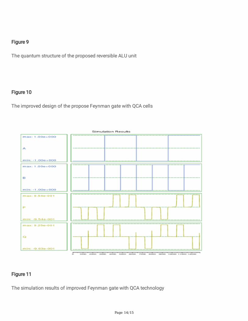
5.1 Simulation of proposed reversible ANG gateIn Figure 11, the implementation of Feynman gate with 14 QCA cells of dimensions of 18 nm, area of0.02 \mu {m}^{2}, in four time zones, and its simulation results are shown. The simulation of proposedANG gate using QCA technology is shown in Figure 12. The performance accuracy of this gate accordingits truth table (Table 2) is shown in Figure 13. The simulation of this gate was performed by 73 cells with18 nm dimensions, area of 0.07 {m}^{2}, and latency of one clock.
5.2 Simulation of proposed reversible ALUThe simulation of proposed reversible ALU base on QCA, in shown in Figure 14. This circuit consists oftwo proposed reversible ANG gates for performing logic and arithmetic operations as well as twoFeynman gates. The simulation of proposed ALU base on QCA was performed with 244 cells, area of0.26 \mu {m}^{2} in four clock pulse zones. The results for simulation of the circuit is shown in Figure 15.
5.3 Evaluation and comparison

Page 10/15
In this section, the proposed ALU unit is compared to existing works in terms of number of operations,latency, number of cells, quantum cost, and occupied area. In previous studies based on QCA, proposedALUs in [6-12], in terms of number of cells, and occupied area, are compared as the best research. Withcomparison in terms of number of cells parameter, the proposed ALU has signi�cant improvementcompared to previous designed ALU. Also, in terms of latency amount and occupied area, the proposedALU has improvement compared to these ALUs. The summary of comparison of proposed ALU withsimulated ALUs using QCA technology is given in Table 5.
Table 5
Comparison of proposed ALU with previous worksReferencedesigns
Total area(µm2 )
Number ofCells
Delay QuantumCost
Number ofOperations
[6] 2.34 1069 12 18 21
[7] 0.78 464 16 14 4
[8] 0.921 670 16 21 16
[11] 0.53 375 12 13 20
[12] 0.48 322 12 12 9
Proposed ALU 0.29 244 6 11 19
6. ConclusionsIn this paper, a reversible Arithmetic and Logic Unit (ALU) is designed, which includes two 3x3 reversiblegates namely ANG gate and two 2x2 Feynman gates. This proposed design includes 275 cells, and areaof 0.29 \mu {m}^{2}. The proposed reversible ALU is simulated in QCA technology. In the QCA design ofthis reversible ALU, an attempt has been made to provide a structure that is optimal in terms of cellnumber, latency and occupied area. In the proposed structure, there are 46% in quantum cost, 44% in cellnumbers, 32% in latency, and 43% in occupied area reductions. The designed ALU includes logicalinstructions: AND, OR, NAND, NOR, NOT, and arithmetic instructions: ADD, SUB, INC. In general, this circuitshows an average more than 68% improvement in terms of evaluation parameters for reversible circuitsand QCA circuits compared to similar works.
References1. Moore, G. E.: Cramming more components onto integrated circuits. Electronics, Volume 38, Number
8, April 19, (1965), Electronics. Retrieved (2011). doi: 10.1109/N-SSC.2006.47858602.

Page 11/15
2. Kunalan, D., Cheong. L. C., Chau, C. F., Ghazali, A. B.: Design of a 4-bit adder using reversible logic inquantum-dot cellular automata (QCA). Semiconductor Electronics (ICSE) (2014). doi:10.1109/SMELEC.2014.6920795
3. Landauer, R.: Irreversibility and Heat Generation in the Computing Processes. IBM J. Res. Develop.(1961) doi: 10.1147/rd.53.0183
4. Sen B, Dutta M, Goswami M, Sikdar BK. Modular design of testable reversible ALU by QCAmultiplexer with increase in programmability. Microelectronics J. 2014;45(11):1522-1532
5. Naresh Chandra Agrawal1, Anil Kumar2 , A. K. Jaiswal, Implementation of Reversible Control and FullAdder Unit Using HNG Reversible Logic Gate, International Journal for Research in Applied Science &Engineering Technology (IJRASET) ISSN: 2321-9653; Volume 5 Issue X, October 2017.
�. Goswami M, Sen B, Mukherjee R, Sikdar BK (2017) Design of testable adder in quantum-dot cellularautomata with fault secure logic. Microelectron J 60:1–12
7. Gadim MR, Navimipour NJ (2018) A new three-level fault tolerance arithmetic and logic unit basedon quantum dot cellular automata. Microsyst Technol 24:1–11
�. Naghibzadeh A, Houshmand M (2017) Design and simulation of a reversible ALU by using QCA cellswith the
9. Oskouei SM, Ghaffari A. Designing a new reversible ALU by QCA for reducing occupation area.Supercomputing. 2019;75(8):5118- 5144.
10. Gadim MR, Navimipour NJ (2018) A new three-level fault tolerance arithmetic and logic unit basedon quantum dot cellular automata. Microsyst Technol 24:1–11
11. Safaiezadeh, B., Mahdipour, E., Haghparast, M. et al. Correction to: Novel design and simulation ofreversible ALU in quantum dot cellular automata. J Supercomput (2021).
12. [13] Norouzi M, Heikalabad SR, Salimzadeh F. A reversible ALU using HNG and Ferdkin gates in QCAnanotechnology. Int J Circ Theor Appl. 2020;1–13. https://doi.org/10.1002/cta.2799
13. Chudasama, A. and T.N. Sasamal. Implementation of 4× 4 vedic multiplier using carry save adder inquantum-dot cellular automata. in Communication and Signal Processing (ICCSP), 2016International Conference on. 2016. IEEE
14. Karkaj, E.T., Heikalabad, S.R.: Binary to gray and gray to binary converter in quantumdot cellularautomata. Optik - Int. J. Light Electron. Opt. 130.doi:10.1016/j.ijleo.2016.11.087 (2017)
15. Asfestani, M.N., Heikalabad, S.R., A unique structure for the multiplexer in quantum-dot cellularautomata to create a revolution, Physica b: Condensed Matter, 512, 91-99.https://doi.org/10.1016/j.physb.2017.02.028
1�. Barughi Z. Y., Heikalabad S. R., A Three-Layer Full Adder/Subtractor Structure in Quantum-DotCellular Automata, International Journal of Theoretical Physics, 56, 9, 2848-2858, 2017.https://doi.org/10.1007/s10773-017-3453-0
17. Ahmad, F., et al., Towards single layer quantum-dot cellular automata adders based on explicitinteraction of cells. Journal of computational science, 2016. 16: p. 8-15.

Page 12/15
1�. Lent, C.S. and P.D. Tougaw, A device architecture for computing with quantum dots. Proceedings ofthe IEEE, 1997. 85(4): p. 541-557.
19. Angizi, S., et al., Novel robust single layer wire crossing approach for exclusive or sum of productslogic design with quantum-dot cellular automata. Journal of Low Power Electronics, 2014. 10(2): p.259-271
20. [21] Mohammadi, Zahra, and Majid Mohammadi. "Implementing a one-bit reversible full adder usingquantum-dot cellular automata." Quantum Information Processing 13.9 (2014): 2127-2147.
21. Walus K, Dysart TJ, Jullien GA, Budiman RA (2004) QCADesigner: a rapid design and simulation toolfor quantum-dot cellular automata. IEEE Trans Nanotechnol 3:26–31
22. Walus K, Dysart TJ, Jullien GA, Budiman RA (2004) QCADesigner: a rapid design and simulation toolfor quantum-dot cellular automata. IEEE Trans Nanotechnol 3:26–31
Figures
Figure 1
QCA cell and two possible polarizations
Figure 2
a Wiring through 90°cells, b wiring using 45° cells
Figure 3
a Simple inverter, b inverter with two effective cells and c two-layer inverter

Page 13/15
Figure 4
a Structure of 3-input majority gate, b 2-input OR gate and c 2-input AND gate [16]
Figure 5
Different Zones of Clocking in QCA [20]
Figure 6
Feynman Gate Layout, a) Internal Circuit, b) Diagram Block
Figure 7
Diagram (a) and quantum (b) structure of ANG proposed reversible gate
Figure 8
Schema of the proposed reversible ALU unit
Page 14/15
Figure 9
The quantum structure of the proposed reversible ALU unit
Figure 10
The improved design of the propose Feynman gate with QCA cells
Figure 11
The simulation results of improved Feynman gate with QCA technology

Page 15/15
Figure 12
The simulation of ANG gate
Figure 13
The simulation results of ANG gate
Figure 14
The simulation of ALU unit designed using QCA cells
Figure 15
The simulation results: a) Inputs b) Outputs