TM 11-5805-637-34 BUFFER, DATA TD-1065/G ... - RadioNerds
73
TM 11-5805-637-34 TECHNICAL MANUAL DIRECT SUPPORT AND GENERAL SUPPORT MAINTENANCE MANUAL BUFFER, DATA TD-1065/G (NSN 5805-01-028-8364) HEADQUARTERS, DEPARTMENT OF THE ARMY 16 APRIL 1981
-
Upload
khangminh22 -
Category
Documents
-
view
1 -
download
0
Transcript of TM 11-5805-637-34 BUFFER, DATA TD-1065/G ... - RadioNerds

TM 11-5805-637-34
TECHNICAL MANUAL
DIRECT SUPPORT AND GENERAL SUPPORT
MAINTENANCE MANUAL
BUFFER, DATA TD-1065/G
(NSN 5805-01-028-8364)
H E A D Q U A R T E R S , D E P A R T M E N T O F T H E A R M Y
16 APRIL 1981

WARNINGDANGEROUS VOLTAGES EXIST IN THIS EQUIPMENT.
Be careful when working on the 115-volt ac line connections. SERIOUS INJURY or DEATH may result from con-tact with these connections.
CAUTIONPlace POWER switch to OFF before removing or inserting circuit card assemblies.
CAUTIONDo not adjust variable controls on any circuit card assembly.
CAUTIONMany data buffer assemblies are secured with captive-type nuts. Do not attempt to turn nuts unless specifically in-structed to do so.

CHANGE
No. 2
TM 11-5805-637-34EE169-JC-lNM-01B/TD 1065B/G
TO 31S5-2G-272C 2
DEPARTMENTS OF THE ARMYTHE NAVY, AND THE AIR FORCE
Washington, DC, 1 August 1988
DIRECT SUPPORT AND GENERAL SUPPORTMAINTENANCE MANUAL
BUFFER, DATATD-1065/G (NSN 5805-01-028-8364)
ANDTD-1065A/G (NSN 5805-01-182-3937)
ANDTD-1065B/G (NSN 5805-01-185-4194)
TM 1l-5805-637-34/EE169-JC-INM-010/TD 1065B/G/TO 31S5-2G-272, 16 April 1981, is changed as follows:
1. Title of manual is changed as shown above.
2. The Navy technical manual identification number (TMIN) has been added to this publication.
3. Remove old pages and insert new pages as indicated below. New or changed material is indicated by a vertical barin the margin of the page. Added or revised illustrations are indicated by a vertical bar adjacent to the identificationnumber.
Remove pages Insert pages
i and ii . . . . . . . . . . . . . . . . . . . . . . . . . . . . . . . . . . . . . . . i and ii1-1 and 1-2 . . . . . . . . . . . . . . . . . . . . . . . . . . . . . . . . . . . . 1-1 and 1-22-5 and 2-6 . . . . . . . . . . . . . . . . . . . . . . . . . . . . . . . . . . . . 2-5 and 2-62-11 through 2-20 . . . . . . . . . . . . . . . . . . . . . . . . . . . . . .2-11 through 2-203-1 through 3-16 . . . . . . . . . . . . . . . . . . . . . . . . . . . . . . . 3-1 through 3-16A-1/(A-2 blank) . . . . . . . . . . . . . . . . . . . . . . . . . . . . . . .A-1/(A-2 blank)
4. File this change sheet in the front of the publication for reference purposes.
Distribution authorized to the Department of defense and DOD contracors onlyfor official use or for administration or operational purposes. This determinationwas made on 13 April 1988. Other requists for this document will be referredto commander, US Army Communications-Electronics command and FortMonmouth, ATTN: AMSEL-LC-ME-P, Fort Monmouth, NJ 07703-5000
DESTRUCTION NOTICE-Destroy by any method that will prevent disclosure ofcontents or reconstruction of the document.

By Order of the Secretaries of the Army, the Navy and the Air Force:
Official:
Official:
R. L. DILWORTHBrigadier General, United States Army
The Adjutant General
CARL E. VUONOGeneral, United States Army
Chief of Staff
WILLIAM CHIAIESEVice Admiral, United States Navy
Commaner, Space and Naval WarfareSystems Command
WILLIAM O. NATIONSColonel, USAF
Director of InformationManagement and Administration
LARRY D. WELSHGeneral, USAFChief of Staf
DISTRIBUTION:To be distributed in accordance with DA Form 12-51 DS/GS
requirements for TD-1065/G.

Change
No. 1
TM 11-5805-637-34TO 31S5-2G-272
C1
DEPARTMENTS OF THE ARMYAND THE AIR FORCE
Washington, DC, 1 January 1986
DIRECT SUPPORT AND GENERAL SUPPORTMAINTENANCE MANUAL
BUFFER, DATATD-1065/G (NSN 5805-01-028-8364)
TD-1065A/G (NSN 5805-01-182-3937)
TM 11-5805-367-34, 16 April 1981, is changed as follows:
1. Title of manual is changed as shown above.
2. The Air Force technical order number has been added to this publication.
3. Remove old pages and insert new pages as indicated below. New or changed material is indicated by a vertical barin the margin of the page. Added or revised illustrations are indicated by a vertical bar in front of the figure caption.
Remove pages Insert pages
i and ii . . . . . . . . . . . . . . . . . . . . . . . . . . i and iil-1and l-2 . . . . . . . . . . . . . . . . . . . . . .. l-l and l-22-1 through 24 . . . . . . . . . . . . . . . . ... 2-l through 242-9 through 2-20 . . . . . . . . . . . . . . . . .. 2-9 through 2-203-11 through 3-16 . . . . . . . . . . . . . . . .. 3-ll through 3-16A-1 . . . . . . . . . . . . . . . . . . . . . . . . . . . .. A-l/(A-2 blank)Figure FO-5 . . . . . . . . . . . . . . . . . . . . .. Figure FO-5Figure FO-8 . . . . . . . . . . . . . . . . . . . . .. Figure FO-8Figure FO-10 . . . . . . . . . . . . . . . . . . . .. Figure FO-10
4. File this change sheet in front of the manual for reference purposes.

By Order of the Secretaries of the Army and the Navy:
Official:
JOHN A WICKHAM, JR.General, United States Army
Chief of Staff
MILDRED E. HEDBERGBrigadier General, United States Army
The Adjutant General
G.B. SCHICK, JR.Rear Admiral, United States Navy
Commander, Naval ElectronicSystems Command
DISTRIBUTION:To be distributed in accordance with DA Form 12-51 literature
requirements for TD-1065/G.

TM 11-5805-637-34EE169-JC-lNM-010/TD 1065B/G
TO 31S5-2G-272
Technical Manual DEPARTMENTS OF THE ARMYNo. 11-5805-637-34 THE NAVY, AND THE AIR FORCETechnical ManualEE169-JC-INM-010/TD 1065B/GTechnical OrderNo. 31S5-2G-272 Washington, DC, 16 April 1981
DIRECT SUPPORT AND GENERAL SUPPORTMAINTENANCE MANUAL
BUFFER, DATATD-1065/G (NSN 5805-01-028-8364)
ANDTD-106SA/G (NSN 5805-01-182-3937)
ANDTD-1065B/G (NSN 5805-01-185-4194)
REPORTING ERRORS AND RECOMMENDING IMPROVEMENTS
You can help improve this manual. If you find any mistakes or if you know of a way to improve theprocedures, please let us know. Mail your letter, DA Form 2028 (Recommended Changes to Publications andBlank Forms), or DA Form 2028-2 located in back of this manual direct to: Commander, US ArmyCommunications-Electronics Command and Fort Monmouth, ATTN: AMSEL-LC-ME-PS Fort Monmouth.NJ 07703-5000.
For Air Force, submit AFTO Form 22 (Technical Order System Publication Improvement Report and Reply)in accordance with paragraph 6-5, Section VI, T.O. 00-5-1. Forward directly to prime ALC/MST.
For Navy, mail comments to the Commander, Space and Naval Warfare Systems Command, ATTN:SPAWAR 8122, Washington, DC 20363-5100.
In either case, a reply will be furnished direct to you.
C H A P T E R 1 .S ECTION I .
II.
C H A P T E R 2 .S E C T I O N I .
II.
CHAPTER 3.S E C T I O N I .
II.
INTRODUCTIONGeneralScope . . . . . . . . . . . . . . . . . . . . . . . . . . . . . . . . . . . . . . . . . . . . . . . . . . . . . . . . . . . . . . . . . . . . . . . . . . .Consolidated index of army publications and blank forms . . . . . . . . . . . . . . . . . . . . . . . . . . . . . . . . . .Maintenance forms, records, and reports . . . . . . . . . . . . . . . . . . . . . . . . . . . . . . . . . . . . . . . . . . . . . . .Reporting equipment improvement recommendations (EIR) . . . . . . . . . . . . . . . . . . . . . . . . . . . . . . . .Administrative storage . . . . . . . . . . . . . . . . . . . . . . . . . . . . . . . . . . . . . . . . . . . . . . . . . . . . . . . . . . . . .Destruction of army electronics materiel . . . . . . . . . . . . . . . . . . . . . . . . . . . . . . . . . . . . . . . . . . . . . . .Description and dataDescription . . . . . . . . . . . . . . . . . . . . . . . . . . . . . . . . . . . . . . . . . . . . . . . . . . . . . . . . . . . . . . . . . . . . .Differences between models . . . . . . . . . . . . . . . . . . . . . . . . . . . . . . . . . . . . . . . . . . . . . . . . . . . . . . . . . . . . . . . .Tabulated data . . . . . . . . . . . . . . . . . . . . . . . . . . . . . . . . . . . . . . . . . . . . . . . . . . . . . . . . . . . . . . . . . . .FUNCTIONING OF EQUIPMENTOverall block diagram discussionIntroduction . . . . . . . . . . . . . . . . . . . . . . . . . . . . . . . . . . . . . . . . . . . . . . . . . . . . . . . . . . . . . . . . . . . . .General . . . . . . . . . . . . . . . . . . . . . . . . . . . . . . . . . . . . . . . . . . . . . . . . . . . . . . . . . . . . . . . . . . . . . . . . .Transmit section . . . . . . . . . . . . . . . . . . . . . . . . . . . . . . . . . . . . . . . . . . . . . . . . . . . . . . . . . . . . . . . . . .Receive section . . . . . . . . . . . . . . . . . . . . . . . . . . . . . . . . . . . . . . . . . . . . . . . . . . . . . . . . . . . . . . . . . . .Fault locator section . . . . . . . . . . . . . . . . . . . . . . . . . . . . . . . . . . . . . . . . . . . . . . . . . . . . . . . . . . . . . . . .Power supply section . . . . . . . . . . . . . . . . . . . . . . . . . . . . . . . . . . . . . . . . . . . . . . . . . . . . . . . . . . . . . . .System timing . . . . . . . . . . . . . . . . . . . . . . . . . . . . . . . . . . . . . . . . . . . . . . . . . . . . . . . . . . . . . . . . . . . .Functional system discussionGeneral . . . . . . . . . . . . . . . . . . . . . . . . . . . . . . . . . . . . . . . . . . . . . . . . . . . . . . . . . . . . . . . . . . . . . . . . .Power supply 19A1 . . . . . . . . . . . . . . . . . . . . . . . . . . . . . . . . . . . . . . . . . . . . . . . . . . . . . . . . . . . . . . . .Fault locator CCA 19A3 . . . . . . . . . . . . . . . . . . . . . . . . . . . . . . . . . . . . . . . . . . . . . . . . . . . . . . . . . . . .Transmit common CCA 19A4 ........ . . . . . . . . . . . . . . . . . . . . . . . . . . . . . . . . . . . . . . . . . . . . . .Receive common CCA 19A5 . . . . . . . . . . . . . . . . . . . . . . . . . . . . . . . . . . . . . . . . . . . . . . . . . . . . . . . . .Channel CCA 19A6, CC19A6A and CCA19A6B . . . . . . . . . . . . . . . . . . . . . . . . . . . . . . . . . . . . . . .High speed filter19A7 . . . . . . . . . . . . . . . . . . . . . . . . . . . . . . . . . . . . . . . . . . . . . . . . . . . . . . . . . . . . .Audio filter19A10 . . . . . . . . . . . . . . . . . . . . . . . . . . . . . . . . . . . . . . . . . . . . . . . . . . . . . . . . . . . . . . . .DIRECT SUPPORT MAINTENANCE INSTRUCTIONSGeneralScope . . . . . . . . . . . . . . . . . . . . . . . . . . . . . . . . . . . . . . . . . . . . . . . . . . . . . . . . . . . . . . . . . . . . . . . . . .Voltage and resistance measurements . . . . . . . . . . . . . . . . . . . . . . . . . . . . . . . . . . . . . . . . . . . . . . . . .Tools and equipmentTools and equipment required . . . . . . . . . . . . . . . . . . . . . . . . . . . . . . . . . . . . . . . . . . . . . . . . . . . . . . . .Coaxial and triaxial cable termination fabrication . . . . . . . . . . . . . . . . . . . . . . . . . . . . . . . . . . . .
Paragraph
1-11-21-31-41-51-6
1-71-7.11-8
2-12-22-32-42-52-62-7
2-82-92-102-112-122-132-142-15
3-13-2
3-33-4
Page
1-11-11-11-11-11-1
1-11-11-2
2-12-12-12-12-22-22-2
2-52-52-52-72-122-142-182-18
3-13-1
3-13-1
EE169-JC-INM-01B/TD 1065B/G/Change 2 i

TM 11-5805-637-34
III. TroubleshootingUse of troubleshooting charts . . . . . . . . . . . . . . . . . . . . . . . . . . . . . . . .Continuity checks . . . . . . . . . . . . . . . . . . . . . . . . . . . . . . . . . . . . . . . . . . . . . . . . . . . . . . . . . . . . . . . . .
IV. Maintenance of data bufferAdjustments . . . . . . . . . . . . . . . . . . . . . . . . . . . . . . . . . . . . . . . . . . . . . . . . . . . . . . . . . . . . . . . . . . . . .Alignment . . . . . . . . . . . . . . . . . . . . . . . . . . . . . . . . . . . . . . . . . . . . . . . . . . . . . . . . . . . . . . . . . . . . . .Repair . . . . . . . . . . . . . . . . . . . . . . . . . . . . . . . . . . . . . . . . . . . . . . . . . . . . . . . . . . . . . . . . . . . . . . . . . .Removal and replacement . . . . . . . . . . . . . . . . . . . . . . . . . . . . . . . . . . . . . . . . . . . . . . . . . . . . . . . . . . .
SECTION V. Direct support testing proceduresIntroduction . . . . . . . . . . . . . . . . . . . . . . . . . . . . . . . . . . . . . . . . . . . . . . . . . . . . . . . . . . . . . . . . . . . . . .Operational test . . . . . . . . . . . . . . . . . . . . . . . . . . . . . . . . . . . . . . . . . . . . . . . . . . . . . . . . . . . . . . . . . . .
SECTION VI. Operational test
C HAPTER
APPENDIX
Figure2-12-22-32-42-52-63-13-23-33-43-53-63-73-83-93-10FO-1FO-2FO-3FO-4FO-5FO-6FO-7FO-8FO-9FO-10FO-11FO-12FO-13(1)FO-13(2)FO-13(3)FO-13(4)FO-13(5)FO-14
Table No.2-12-23-13-23-3
Paragraph
3-53-6
3-73-83-93-10
3-113-12
Introduction . . . . . . . . . . . . . . . . . . . . . . . . . . . . . . . . . . . . . . . . . . . . . . . . . . . . . . . . . . . . . . . . . . . . . . . . . 3-13Set-Up for Test Set Error Detector, andSG-1139/G Digital Data Generator. . . . . . . . . . . . . . . . . . . . . . . . . . . . . . . . . . . . . . . . . . . . . . . . . . . . 3-14Operation when using TS-3981/P or SG-1139/G . . . . . . . . . . . . . . . . . . . . . . . . . . . . . . . . . . ....Test
3-15. . . . . . . . . . . . . . . . . . . . . . . . . . . . . . . . . . . . . . . . . . . . . . . . . . . . . . . . . . . . . . . . . . . . . . . . . . . . . . . . 3-16
16KB/S 2 wire tests TD-1065( )/G . . . . . . . . . . . . . . . . . . . . . . . . . . . . . . . . . . . . . . . . . . . . . . . . 3-174. GENERAL SUPPORT MAINTENANCE INSTRUCTIONS
A. REFERENCES . . . . . . . . . . . . . . . . . . . . . . . . . . . . . . . . . . . . . . . . . . . . . . . . . . . . . . . . . . . . . . . . . . . . . . . . . . . . . . . .B. REPAIR PARTS AND SPECIAL TOOLS NON-APPLICABLE
LIST OF ILLUSTRATIONS
Data buffer control channel format, 12 channeloperation. . . . . . . . . . . . . . . . . . . . . . . . . . . . . . . . . . . . . . . . . . . .Data buffer control channelformst, six-channeloperation . . . . . . . . . . . . . . . . . . . . . . . . . . . . . . . . . . . . . . . . . . .Power supply19Al, functional block diagram.. . . . . . . . . . . . . . . . . . . . . . . . . . . . . . . . . . . . . . . . . . . . . . . . . . . .Transmit common CCA 19A4, overall functional block diagram. . . . . . . . . . . . . . . . . . . . . . . . . . . . . . . . . . . . . . .High speed filter 19A7, functional block diagram . . . . . . . . . . . . . . . . . . . . . . . . . . . . . . . . . . . . . . . . . . . . . . . . . .Audio filter 19A10, functional block diagram. . . . . . . . . . . . . . . . . . . . . . . . . . . . . . . . . . . . . . . . . . . . . . . . . . . . .Data buffer, rear view . . . . . . . . . . . . . . . . . . . . . . . . . . . . . . . . . . . . . . . . . . . . . . . . . . . . . . . . . . . . . . . . . . . . . . . . .Removal and replacement of ac line filter and alarm relay. . . . . . . . . . . . . . . . . . . . . . . . . . . . . . . . . . . . . . . . . . . .Printed circuit card guides, front view. . . . . . . . . . . . . . . . . . . . . . . . . . . . . . . . . . . . . . . . . . . . . . . . . . . . . . . . . . .Printed circuit card guides, rear view. . . . . . . . . . . . . . . . . . . . . . . . . . . . . . . . . . . . . . . . . . . . . . . . . . . . . . . . . . .Removal and replacement of front panel components . . . . . . . . . . . . . . . . . . . . . . . . . . . . . . . . . . . . . . . . . . . . . . .Power supply assembly, top rear view. . . . . . . . . . . . . . . . . . . . . . . . . . . . . . . . . . . . . . . . . . . . . . . . . . . . . . . . . . .Power supply assembly, front view. . . . . . . . . . . . . . . . . . . . . . . . . . . . . . . . . . . . . . . . . . . . . . . . . . . . . . . . . . . . .Power supply assembly, bottom view. . . . . . . . . . . . . . . . . . . . . . . . . . . . . . . . . . . . . . . . . . . . . . . . . . . . . . . . . . . .16/32 KM/S 4W lests TD-66A/G16/KB/S 2W testData buffer, overall block diagram . . . . . . . . . . . . . . . . . . . . . . . . . . . . . . . . . . . . . . . . . . . . . . . . . . . . . . . . . . . . .TD 660( )/G frame format, six and 12-channel... . . . . . . . . . . . . . . . . . . . . . . . . . . . . . . . . . . . . . . . . . . . . . . . .Fault locator CCA 19A3, functional block diagram . . . . . . . . . . . . . . . . . . . . . . . . . . . . . . . . . . . . . . . . . . . . . . . . .Transmit common CCA l9A4 (input/select section), functional block diagmm. . . . . . . . . . . . . . . . . . . . . . . . . . . .Combining channel process timing, six and12-channel. . . . . . . . . . . . . . . . . . . . . . . . . . . . . . . . . . . . . . . . . . . . . .Transmit common CCA 19A4 (ouput/timing section), functional block diagram . . . . . . . . . . . . . . . . . . . . . . . . . .Receive common CCA l9A5, functional block diagram.............. . . . . . . . . . . . . . . . . . . . . . . . . . . . . . . . . .Channel CCA 19A6. CC19A6A and CCAT9A6B (transmit section), functional block diagram . . . . . . . . . . . . . . . .Channel CCA 19A6 (receive section), functional block diagram . . . . . . . . . . . . . . . . . . . . . . . . . . . . . . . . . . . . . . . .Data buffer, System test diagram . . . . . . . . . . . . . . . . . . . . . . . . . . . . . . . . . . . . . . . . . . . . . . . . . . . . . . . . . . . . .
Power supply 19Al, schematic diagam . . . . . . . . . . . . . . . . . . . . . . . . . . . . . . . . . . . . . . . . . . . . . . . . . . . . . . . . .Power supply 19A1, wiring diagram . . . . . . . . . . . . . . . . . . . . . . . . . . . . . . . . . . . . . . . . . . . . . . . . . . . . . . . . . . . .Data buffer, overall schematic diagram (sheet l of 5) . . . . . . . . . . . . . . . . . . . . . . . . . . . . . . . . . . . . . . . . . . . . . . . . . . . . . . . .Data buffer, overall schematic diagram (sheet 2 of 5) . . . . . . . . . . . . . . . . . . . . . . . . . . . . . . . . . . . . . . . . . . . . . . .Data buffer, overall schematic diagram (sheet 3 of 5) . . . . . . . . . . . . . . . . . . . . . . . . . . . . . . . . . . . . . . . . . . . . . .Data buffer, overall schematic diagram(sheet 4 of 5) . . . . . . . . . . . . . . . . . . . . . . . . . . . . . . . . . . . . . . . . . . . . . . .Datas buffer, overall schematic diagram(sheet 5 of 5) . . . . . . . . . . . . . . . . . . . . . . . . . . . . . . . . . . . . . . . . . . . . . . .Standard color coding chart . . . . . . .. . . . . . . . . . . . . . . . . . . . . . . . . . . . . . . . . . . . . . . . . . . .
Signals monitored by fault locator CCA . . . . . . . . . . . . . . . . . . . . . . . . . . . . . . . . . . . . . . . . . . . . . . . . . . . . . . . . . .Signal versus channel assignments. . . . . . . . . . . . . . . . . . . . . . . . . . . . . . . . . . . . . . . . . . . . . . . . . . . . . . . . . . . .Data buffer troubleshooting chart . . . . . . . . . . . . . . . . . . . . . . . . . . . . . . . . . . . . . . . . . . . . . . . . . . . . . . . . . . . . . .Power supply troubleshooting chart . . . . . . . . . . . . . . . . . . . . . . . . . . . . . . . . . . . . . . . . . . . . . . . . . . . . . . . . . . . .Connections for data buffer operetional test . . . . . . . . . . . . . . . . . . . . . . . . . . . . . . . . . . . . . . . . . . . . . . . . . . . . . .
Page
3-13-2
3-43-43-43-4
3-113-11
3-13
3-133-133-143-14
. . . . . . A-1B-l
Page2-32-42-62-82-192-203-43-53-63-73-83-93-103-123-153-16
Located inBack ofManual
Located inBack ofManual
Page2-52-133-23-33-13
ii Change 2

TM 11-5805-637-34
CHAPTER 1
INTRODUCTION
1-1 Scope
Section I. GENERAL
This manual contains a functional description and directsupport and general support maintenance instructionsfor Buffer, Data TD-1065/G, TD-1065A/G andTD-1065B/G. The Buffer, Data is referred to as databuffer in this manual. Appendix A lists the publicationsapplicable to this equipment,
1-2. Consolidated Index Of Army Publica-tions And Blank Forms
Refer to the latest issue of DA Pam 25-30 to determinewhether there are new editions, changes, or additionalpublications pertaining to the equipment.
1-3. Maintenance Forms, Records, andRoports
a. Reports of Maintenance and Unsatisfactory Equip-ment. Department of the Army forms and proceduresused for equipment maintenance will be those prescribedby DA Pam 738-750 as contained in MaintenanceManagement Update. Air Force personnel will use AFR66-1 for maintenance reporting and TO-O-35D54 forunsatisfactory equipment reporting. Navy personnel willreport maintenance performed utilizing the MaintenanceData Collection Subsystem (MDCS) LAW OPNAVINST4790.2, Vol 3 and unsatisfactory material/conditions(UR submissions) LAW OPNAVINST 4790.2, Vol 2,chanter 17.
b. Report of Packaging and Handling Deficiencies.Fill out and forward SF 364 (Report of DiscrepancyROD)) as prescribed in AR 735-1l-2/DLAR 4140.55/NAVMATINST 4355.73B/AFR400-54/MCO 4430.3H.
c. Discrepancy in Shipment Report (DISREP)(SF361). Fill out and forward Discrepancy in ShipmentReport (DISREP) (SF 361) as prescribed in AR 55-38/NAVSUPINST 4610.33C/AFR 75-18/MCOP4610.19D/DLAR-4500.15.
1-4. Reporting Equipment ImprovementRecommendations (EIR)
If your equipment needs improvement let us know. Sendus an EIR. You, the user, are the only one who can tell uswhat you don’t like about the design. Put it on an SF 368 .(Quality Deficiency Report). Mail it to Commander, USArmy Communications-Electronics Command and FortMonmouth, ATTN: AMSEL-PA-MA-D, Fort Mon-mouth, New Jersey 07708-5000. We’ll send you a reply.
1-5. Administrative StorageAdministrative Storage of Equipment issued to and usedby Army activities will have preventive maintenanceperformed in accordance with the PMCS charts ascovered in TM 11-5805-637-12 before storing. Whenremoving the equipment from administrative storage thePMCS should be performed to assure operational readi-ness. Disassembly and repacking of equipment for shipment or limited storage is covered in TM 11-5805-637-12and TM 750-244-20.
1-6. Destruction of Army Electronics Mat-eriel
Destruction of Army electronics materiel to preventenemy use shall be in accordance with TM 750-244-2.
Section Il. DESCRIPTION AND DATA
1-7. Description
Refer to TM 11-5805-637-12 for a description of thea. Only the TD-1065A/G containing circuit card
data buffer.assembly channel unit, CCA19A6A, or the TD-1065B/Gwith circuit card assembly channel unit CCA19A6B
1-7.1 Differences Between Models can be used in conjunction with central office telephoneNOTE automatic AN/TCC-39.
Except where indicated Buffer, Data TD-1065/G NOTEinformation referenced in this manual relates to the Except where indicated CCA19A6 informationBuffer, Data TD-1065A/G and the TD-1065B/G referenced in this manual relates to the CCA19A6Aas well. and CCA19A6B as well.
Change 2 1-1

TM 11-5805-637-34
b. Functional characteristics are as follows. (3) TD-l065B/G with CCA19A6B provides TD-
(1) TD-1065/G with CCA19A6 provides full duplex 1065/G operation (Mode A) or TD-1065/G operation
operation for 16KB and 32KB data (4W) or half duplex (Mode B).
operation for 16KB data and full duplex operation for32KB data (2W).
(2) TD-1065A/G with CCA19A6A provides full 1-8. Tabulated Data
duplex operation for 32KB data (4W) or half duplex Refer to TM 11-5805-637-12 for tabulated data pertainingoperation for 16KB data (2W). to the data buffer.
1-2 Change 2

TM 11-5805-637-34TO 31S5-2G-272
CHAPTER 2
FUNCTIONING OF EQUIPMENT
Section I. OVERALL BLOCK DIAGRAM DISCUSSION
2-1. IntroductionThis chapter provides a functional description of thedata buffer. It includes an overall block diagram dis-cussion and a functional system discussion with de-tailed block diagram descriptions of each functionalelement in the data buffer.
2-2. General(fig. FO-1)
a. The data buffer is used in conjunction with multi-plexer TD-660( )/G. This permits the data buffer tooperate with both voice and data signals. TheTD-660( )/G may be used in a six-channel or a 12-channel mode of operation. The TD-660( )/G multi :
plexes and encodes up to six or 12 four-wire voice fre-quency channels into a single time-division-multiplexpulse-code-modulation (tdm/pcm) channel. This takesplace in the TD-660( )/G transmit section. Converse-ly, the TD-660( )/G receive section demultiplexes anddecodes a tdm/pcm channel to provide up to six or 12four-wire voice frequency channel outputs. The databuffer automatically compensates for either six-chan-nel or 12-channel operation. If the data buffer becomesinoperative, operating the data buffer power ON/OFFcircuit breaker to OFF restores relays that route in-coming signals around the data buffer. This permitsthe TD-660( )/G to operate normally with voice andtdm/pcm signals.
b. The data buffer is comprised of four functionalsections: transmit, receive, fault locator, and powersupply. Both the transmit and receive sections utilizesignals provided by the TD-660( )/G. The fault loca-tor and power supply provide maintenance service andpower to functional blocks of the data buffer.
2-3. Transmit Sectiona. The transmit section receives up to six or 12
channels of diphase data/voice signals. These signalsare processed in conjunction with the TD-660( )/G tocombine them into a single output channel containingsix or 12 channels of the tdm data and pcm signals.
b. Up to six or 12 channels of diphase data/voice sig-nals are applied to the data buffer audio filter. The au-dio filter routes voice input signals to theTD-660( )/G and routes diphase data to an associateddata buffer channel circuit card assembly (CCA). Theaudio filter also serves to reduce electromagnetic inter-
ference radiating from the data buffer. It also reducesundesirable radiation of signals containing data orvoice information.
NOTEEach channel CCA has one transmit sectionand one receive section. For 12-channeloperation, all 12 channel CCAs are used toprocess data. For six-channel operation, onlythe odd-numbered channel CCAs are used toprocess data.
c. Each channel CCA converts diphase data to bi-nary data, adjusts the data rate, and structures thedata so that it can be inserted into the multiplexedpcm signal. The channel CCA then applies the data(now in binary format) to the transmit common CCA.The TD-660( )/G converts the voice channels fromthe audio filter into a single tdm/pcm channel. TheTD-660( )/G then applies the pcm channel, alongwith timing and address lines to the high speed filter.The high speed filter provides filtering for the pcm,timing, and address signals. The high speed filter thenapplies these signals to the transmit common CCA.The high speed filter also serves to reduce electromag-netic interference radiating from the data buffer. Italso reduces undesirable radiation of signals contain-ing voice or data information.
d. The transmit common CCA examines the datafrom the channel CCAs to determine mode of opera-tion (six or 12 channel). It automatically adjusts toeither mode, then inserts the active binary data chan-nels into the empty pcm time slots from the high speedfilter. This forms a single combined multiplexed dataand pcm channel. The combined channel is applied toanother section of the high speed filter. Here it is fil-tered and applied to the data buffer output along withthe address and timing lines.
2-4 Receive Sectiona. The TD-660( )/G accepts a multiplexed
pcm/data channel and its corresponding timing line.The TD-660( )/G demultiplexes and decodes thepcm/data channel. It applies the voice channels direct-ly to the audio filter. It also applies the multiplexeddata, along with timing and address, to the high speedfilter.
b. The high speed filter filters and routes the data tothe receive common CCA. Here, the data is examined
CHANGE 1 2-1

TM 11-5805-637-34
for mode (six or 12 channel). After adjusting to eithermode, the receive common CCA retimes the data andapplies it to an associated channel CCA. The channel
CCAs convert the data to the source frequency (16 kb/sor 32 kb/s) and from binary form to diphase. The di-phase data channels are then applied to the audio fil-ter.
c. The audio filter routes voice channels from theTD-660( )/G directly to associated data buffer out-puts. The active data channels from the channel CCAsare impedance matched by the audio filter. The datachannels are then routed to associated data buffer out-puts,
2-5. Fault Locator SectionThe fault locator CCA provides a means of determin-ing the operational status of the data buffer. In theevent of a failure, it aids in locating the cause of thefault. A front panel ALARM indicator lamp illumi-nates when built-in test equipment (BITE) detects afault condition. A front panel TEST indicator lamp isused in conjunction with BITE features to localize afault.
2-6. Power Supply SectionThe power supply converts a 115 Vac power input to±10 Vdc to supply power to all data buffer circuits.
2-7. System TimingThe following paragraphs describe overall system tim-ing and formatting. Both timing generated by theTD-660( )/G and timing generated by the data bufferare discussed.
a. TD-660( )/G Frame Format. Figure FO-2 illus-trates the pcm frame format of the TD-660( )/G forboth six and 12-channel operation. For 12-channeloperation, each frame consists of 12 channels. For six-channel operation, each frame consists of six channels.The frame length is the same for either six or 12-chan-nel operation. So that six channels may occupy thesame time span as 12 channels, the channels are ex-panded for six-channel operation. Each channel in thesix-channel mode frame occupies the same time spanas two channels in the 12-channel mode frame. Thechannel bit structure remains the same for either thesix or 12-channel mode frame. Each channel containssix bits. The six bits comprise a pcm word representa-tive of the voice information contained in that chan-nel. The sixth bit of the last channel in each frame(channel 6 or channel 12) is used as a framing bit. Theframing bit signifies the end of the frame.
b. Data Buffer Control Channel Format. Figure 2-1illustrates the format of receive inputs to, and trans-mit outputs of, the data buffer during 12-channel
operation. Figure 2-2 illustrates the format of receiveinputs to, and transmit outputs of, the data buffer dur-ing six-channel operation. The data buffer format isexactly the same for either six or 12-channel opera-tion, except for the number of channels per frame. Asin the TD-660( )/G frame format, each six-channelmode frame contains six channels, while each 12-chan-nel mode frame contains 12 channels. The format illus-trated represents a data buffer control channel, whichis comprised of the fifth bit from 16 consecutiveTD-660( )/G frames. The control channel contains in-formation that indicates mode (data or voice) and datarate (16 kb/s or 32 kb/s in the data mode) for each ofthe six or 12 channels. The control channel also con-tains information that controls data synchronizationinformation in the data mode. Channel 1 is shown con-taining data in these examples; channel 2 is showncontaining pcm. In actual operation, any channel cancontain either data or pcm. The following discussion islimited to channels 1 and 2. However, this discussionalso applies to channels 3 through 6 for six-channeloperation, or 3 through 12 for 12-channel operation.
(1) Data channel. A typical data channel is shownin figures 2-1 and 2-2 as channel 1. The first four bitscontain data; the fifth bit is used for control channelfunctions. Bit 5 in frames 1 through 7 is a marker bitthat makes up a 7-bit word that indicates rate andmode. A 1110010 pattern indicates a 32 kb/s data rate.A 0001101 pattern indicates a 16 kb/s data rate. Anyother pattern indicates the voice mode. Bit 5 in frames8 through 14 is a signaling bit indicating that either astuff or a spill operation has been performed. Thestuff/spill operation is a method of synchronizationthat permits the data buffer to operate with asynchro-nous data rates. During a stuff operation, bit 1 inframe 16 is repeated in the bit 2 position. It is then ig-nored by the receiving equipment. During a spilloperation, a data bit is inserted in the bit 5 position inframe 15. This bit is recovered by the receiving equip-ment and reinserted into its proper time slot. Either astuff or spill operation is performed on each data chan-nel. When the incoming data rate is slower than therate required by the data buffer, more stuff operationsare performed than spill operations. Conversely, whenthe incoming data rate is faster than the rate requiredby the data buffer, more spill operations are per-formed than stuff operations.
(2) PCM channel. A typical pcm data channel isshown in figures 2-1 and 2-2 as channel 2. All six bitsof a pcm channel contain encoded voice information ineach TD-660( )/G frame. The data buffer recognizesthe voice mode by the absence of either a 1110010 or0001101 pattern as explained in paragraph 2-b.(1).
2 - 2

Figure 2-1.
TM
11
-58
05
-63
7-3
4T
O 3
1S
5-2
G-2
72
CH
AN
GE
1
2-3

Figure 2-2.
TM 11-5805-637-34
TO 31S5-2G-272
2-4CHANGE 1

TM 11-5805-637-34
Section II. FUNCTIONAL SYSTEM DISCUSSION
2-8 GeneralThe data buffer is comprised of four different CCAsand three replaceable assemblies as follows:
a. Power Supply 19A1b. Fault locator CCA 19A3c. Transmit common CCA 19A4d. Receive common CCA 19A5e. Channel CCA19A6, CCA19A6A, or 19A6Bf. High speed filter 19A7g. Audio filter 19A10
Each CCA and replaceable assembly is described in thefollowing paragraphs.
2-9. Power Supply 19A1(fig. 2-3)
The power supply converts 115 Vac, 50-400 Hz powerto ±10 Vdc. The ±10 Vdc is distributed throughoutthe data buffer. The power supply receives 115 Vacpower from line filter 19FL1 and overvoltage ab-sorbers 19RV1 and 19RV2. The line filter reduces elec-tromagnetic interference entering or leaving the databuffer. The overvoltage absorbers protect the powersupply from excessive input voltage transients. The
115 Vac input is applied through POWER ON/OFF cir-cuit breaker CB1 to stepdown transformer T1. Theoutput of transformer T1 is applied to diode bridgeCCA 19A1A2. The diode bridge CCA contains two fullwave bridge rectifiers. The outputs of the two recti-fiers are applied through filter CCA 19A1A1 to reduceripple.
2-10. Fault Locator CCA 19A3(fig. FO-3)
a. The fault locator CCA monitors the statue of 22signals within the data buffer. These signals indicatethe operational status of data buffer CCAs and assem-blies, and are listed in table 2-1. A fault in any ofthese signals, except +10V and -10V, enables bothan audible alarm and an external remote alarm. Afault condition also causes a front panel ALARM indi-cator lamp to illuminate. A fault condition in any ofthese signals can be localized by positioning a frontpanel rotary switch to each of 10 positions. A frontpanel TEST indicator lamp illuminates to indicate thatthe signal associated with the selected switch positionis present.
Table 2-1. Signals Monitored by Fault Locator CCA
b. Six signals from high speed filter 19A7 are ap- Input Signalplied to the buffers and amplifiers. The buffers and BAUXAD
amplifiers convert these pulse signals to logic levels BTXPCM
that indicate the presence or absence of the signals. BTXTIM
The buffers and amplifier outputs are related to theirBRXADBRXPCM
inputs as follows BRXTIM
Output SignalTXPRMM (transmit framing monitor)TXPCMM (transmit pcm monitor)TXTIMM (transmit timing monitor)RXFRMM (receive framing monitor)RXPCMM (receive pcm monitor)RXTIMM (receive timing monitor)
Change 2 2-5

2-6
TM 11-5805-637-34
Figure 2-3. Power supply 19A1, functional block diagram.

TM 11-5805-637-34
The outputs of the buffers and amplifiers are com-bined in the NAND gates to produce a relay controlenable signal. This signal is present only when all in-put signals, including CCMTR (common circuit moni-tor), are present. Absence of the relay control signal in-dicates an alarm condition. The relay control enablesignal is applied to the l-second delay circuit. When allinputs are present, the l-second delay circuit producesa DLY (delay) signal. Loss of an input causes the DLYsignal to be removed after a delay of 1 second.
c. When the DLY signal is present, the relay controlenable circuit produces two outputs: RLYDRV (relaydrive) and alarm disable. The RLYDRV signal causesalarm relay 19K1 to operate. This extinguishesALARM indicator lamp 19DS1 and disables the re-mote alarm signal. The alarm disable signal disablesthe audible alarm circuit. Loss of DLY results in loss ofthe RLYDRV and alarm disable signals. Loss ofRLYDRV restores the alarm relay, thereby illuminat-ing the ALARM indicator and enabling the remotealarm. Loss of the alarm disable signal enables theaudible alarm circuit. A SPKRDR (speaker drive) sig-nal is then applied to loudspeaker 19LS1 to produce analarm tone. The alarm tone can be silenced by depress-ing alternate-action BUZZER OFF pushbutton switch19S2. At any time, the audible alarm can either be ac-tivated or silenced by alternately depressing and re-leasing the BUZZER OFF pushbutton switch. Whenthe data buffer is initially turned on, the unit power-onalarm enable circuit momentarily generates an alarmcondition. This occurs when +10V from power supply19A1 momentarily generates a power-on alarm signal.This is applied to the relay control circuit, and gen-erates an alarm for the duration of the power-on alarmsignal.
d. Two signals are applied to the common circuitalarm detector. These are TXCOMM from transmitcommon CCA 19A4, and RXCOMM from receive com-mon CCA 19A5. When both signals are present, aCCMTR signal enables the NAND gates. Loss of eitherTXCOMM or RXCOMM removes CCMTR, which alsoremoves the relay control enable signal. This generatesan alarm as previously described.
e. The channel alarm detector receives one CUAL(channel alarm) signal from each of 12 channel CCAs19A6. When all CUAL signals are present, a CCHMTR(channel monitor) signal is applied to the relay controlcircuit. Loss of any CUAL signal removes CCHMTRand generates an alarm as previously described.
f. The 10-volt monitor circuit receives +10V and-10V from power supply 19A1. This circuit evaluatesthe amplitude of the ±10 volts, and produces two out-put signals if the ±10 volt input is above a set lowerlimit. These signals, +10VMTR (+10 volt monitor)and -10VMTR (-10 volt monitor), are applied to ro-tary switch 19S1.
g. Ten fault locator monitor signals are applied tothe rotary switch. These signals are:
(1) CCHMTR(2) +10VMTR(3) -10VMTR(4) CCMTR(5) TXFRMM(6) TXPCMM(7) TXTIMM(8) RXFRMM(9) RXPCMM(10) RXTIMM
Any one of these signals can be selected by the rotaryswitch. The selected signal is applied to the lampdriver as signal MTRINP (monitor input). If MTRINPis present, the lamp driver generates FLTLMP (faultlamp) to illuminate TEST indicator lamp 19D2. Theabsence of the selected signal removes MTRINP andFLTLMP and extinguishes the TEST indicator lamp.
2-11. Transmit Common CCA 19A4a. General. The transmit common CCA, figure 2-4,
is divided into two functional sections, These are (1)the input/select section, and (2) the output/timing sec-tion. The input/select section receives six or 12 chan-nels of pcm. It also receives six or 12 channels of multi-plexed data. These signals are combined into a singletdm output signal of data and pcm. The combineddata/pcm signal is applied to the output/timing sectionwhere it is retimed for proper phasing. The out-put/timing section also generates clocks which controltiming functions on each channel CCA 19A6.
(1) The input/select section operates in one of twomodes, six channel or 12 channel. The operating modeis determined by the frequency of signal BTXTIM. Inthe six-channel mode, BTXTIM, along with the incom-ing data, rate, and occupancy signals, must be restruc-tured. Restructuring serves two purposes. First, it al-lows the input/select section to deliver a selected tim-ing signal at the 12-channel rate. This is then used toderive the channel CCA interface signals. Also, re-structuring is necessary to expand six channels of datainto a 12-channel frame length. After restructuring,data is combined with BTXPCM into a single tdm sig-nal. Occupancy (stuff/spill signaling) bits or rate (16kb/s or 32 kb/s) bits are also inserted into bit 5 of eachdata channel during the combining process. These bitsconstitute the data buffer’s control channel. See para-graph 2-7b. for an explanation of the control channelformat. In the 12-channel mode, data and pcm aresimilarly combined. However, the signals are not firstrestructured. The selected timing signal is applied tothe output/timing section. The selected and combinedpcm and data signal is also applied to the output/tim-ing section. Address signal BAUXAD is retimed and
2-7

TM 11-5805-637-34
2-8
Figure 2-4. Transmit common CCA 19A4, overall functional block diagraJm.

TM 11-5805-637-34TO 31S5-2G-272
applied to the output/timing section as a retimed ad-dress signal. The delay is necessary for proper phasingwith both pcm and data signals. The input/select sec-tion also produces an error signal to indicate a problemin the six-channel mode timing circuits.
(2) The output/timing section uses the selectedtiming and retimed framing signals to produce threegroups of channel CCA control clocks. These are: thechannel control clocks, the stuff/spill clocks, and theframe control clocks. The channel control, clocks con-trol channel timing and elastic store read-in timing ineach channel CCA (transmit section). The stuff/spillclocks control stuff and spill operation timing in eachchannel CCA (transmit section). Finally, the framecontrol clocks control frame timing, and control chan-nel timing in each channel CCA (transmit section). Theoutput/timing section also retimes the selected andcombined pcm and data signal, and the retimed ad-dress signal. Retiming is necessary so that the cor-responding pcm and address output signals, BPCMOTand BXADOT, are properly phased. BITE circuits inthe output/timing section monitor the error signalfrom the input/select section. If an error is indicated,output signal TXCOMM signals fault locator CCA19A3 to produce an alarm. The BITE circuits alsomonitor several timing functions internal to the out-put/timing section. Errors in these monitored timingfunctions also produce TXCOMM and generate analarm.
b. Input/Select Section. The input/select section, fig-ure FO-4, operates in one of two modes: six channel or
12 channel. The data buffer must be able to recognizewhether the incoming data is structured in a six-chan-
nel format or a 12-channel format. It accomplishes thisby counting the number of transmit timing pulses con-tained in one frame. A 12-channel frame contains 72pulses, while a six-channel frame contains only 36pulses. When the format has been determined, themode is selected by one of two enable signals and datais processed accordingly.
(1) Mode Selection. Transmit timing signalBTXTIM, from high speed filter 19A7, is applied tothe pulse stretcher/shaper. The pukes are stretchedand applied to the 6/12-chan mode select circuit as sig-nal PRIDLY (primary delay). The 6/12-chan modeselect circuit counts the number of PRIDLY pukescontained in one frame. Information on frame lengthis obtained from signal BAUXAD. If the 6/12-chanmode select circuit counts 72 PRIDLY pulses per milli-second a 12-chan enable signal is produced. If the 6/12-chan mode select circuit counts 36 PRIDLY pulses permillisecond, a 6-than enable signal is produced. Theenable signals are applied to the 6/12-than signal selectorto select the proper set of signals for the mode of operation.Both enable signals are also used by the output/timing
section to enable one of two phase adjust circuits.
(2) Transmit Timing. Input signal BTXTIM isstretched to become signal PRIDLY as previously de-scribed. In the 12-channel mode, PRIDLY will be 576KHz. In this case, PRIDLY is applied directly to the6/12-chan signal selector. The 12-chan enable signalthen causes the 6/12-chan signal selector to routePRIDLY to output TCLK (transmit clock). TCLK isdistributed to various input/select and output/timingsection circuits. In the six channel mode, PRIDLY willbe only 288 KHz. In order to ensure proper timing,TCLK must always be 576 KHz. To achieve this, PRID-LY is applied to the frequency doubler. The frequencyof PRIDLY is doubled to 576 KHz and applied to the6/12-chan signal selector as signal PLL (phase-locked-loop). The 6-chan enable signal then causes the 6/12-chan signal selector to route PLL to output TCLK. Theaccuracy of the frequency doubler is monitored in thesix-channel mode. As long as the frequency doubler isoperating properly, a lock signal is applied to the lock-in detector. Signal PRIDLY ia also applied to the lock-in detector. If the frequency doubler is not operatingproperly, the lock-in detector produces an error signal.The error signal is applied to the BITE circuit in theoutput/timing section. During the 12-channel mode,the 12-chan enable signal is applied to the lock-in de-tector. This inhibits the lock-in detector from erro-neously producing the error signal during the 12-chan-nel mode. In either mode, signal PRIDLY is routed tothe output/timing section. It is used by the phase ad-just circuits to provide a pcm delay clock.
(3) Transmit PCM. Transmit pcm signalBTXPCM, from high speed filter 19A7, is applied tothe pcm retiming circuit. The pcm retiming circuituses TCLK to retime BTXPCM. This delays BTXPCMso that it may be properly combined with either six or12-channel data. The output of the pcm retiming cir-cuit, signal pcm, is then applied to the combining cir-cuits and the 6-chan data/voice select circuit. These cir-cuits are used to combine the pcm signal with either12-channel or six-channel data, respectively.
(4) Transmit Data, 12-Channel Mode. In the 12-channel mode, the combining circuits are used to com-bine data bits with occupancy (stuff/spill signaling)and rate (16 kb/s or 32 kb/s) bits. The data channels arethen combined with pcm channels into a single 12-channel data/pcm signal. Data bits from each channelCCA 19A6 are applied to the DBUS retiming circuit assignal DBUS (data bus). The DBUS retiming circuituses signal TCLK to retime the DBUS signal. The re-timed data bits are applied to the combining circuits.Signals OBUS (occupancy bus) and RBUS (rate bus)are also applied to the combining circuits. The combin-ing circuits multiplex the data bits with the signalingbits contained in OBUS and RBUS. A bit 5 gate pulseand a marker signal from the output/timing sectionare applied to the combining circuits to control signal-
CHANGE 1 2-9

TM 11-5605-637-34
ing bit insertion. Of the six bits contained in eachTD-660( )/G channel time slot, data bits are insertedinto the first four. The fifth bit is a control bit. It re-ceives either rate information from RBUS orstuff/spill signaling information from OBUS. Duringframe 15, the control bit may be a valid data bit. If so,signal frame 15 causes the valid data bit (spill bit) to beinserted into its proper control channel time slot. Thesixth bit is unused and is ignored by the receivingequipment. It is inhibited by a pulse derived from thechannel control clocks (signal clocks) from the out-put/timing section. This inhibit pulse allows the sixthbit of a pcm word to pass through the combining cir-cuits. The combined data and control bit informationfrom each active data channel is then multiplexed withthe active pcm channels. The data/pcm combiningprocess is controlled by a delayed mode signal derivedfrom MBUS (mode bus). MBUS contains informationon the mode (data or voice) of each channel. MBUS isapplied to the data-to-analog switchover delay circuit.As long as the state of MBUS remains constant for aparticular channel, the delayed mode signal will alsoremain constant. If the state of MBUS changes fromvoice to data for a particular channel, the delayedmode signal will also change immediately. However, ifthe state of MBUS changes from data to voice for aparticular channel, a delay is introduced. This delay isgenerated using several clocks from the output/timingsection. The delay is necessary to compensate for data-to-voice switchover delays introduced by each channelCCA 19A6. The delayed mode signal is then applied tothe combining circuits. If the state of the delayedmode signal shows that a channel contains voice in-formation (pcm), the pcm signal is gated into thatchannel’s time slot. If the state of the delayed modesignal shows that a channel contains data, the com-bined data and control bits are gated into thatchannel’s time slot. The combined 12-chan data/pcmsignal is applied to the 6/12-chan signal selector. The
12-chan enable signal then causes the 6/12-chan signalselector to route the 12-chan data/pcm signal to outputTDATA (transmit data). Figure FO-5A shows thestructure of signal TDATA during a typical 12-channelframe. In the example, channels 4, 8, 9, and 12 areshown as voice channels while the remaining channelsare shown as data channels. In actual operation, how-ever, any channel could contain either data or voice.As previously described, the first four bits of each datachannel are shown containing data bits. The fifth bit isshown containing control information from eitherOBUS or MBUS. The sixth bit is unused. All six bits ofeach voice channel are shown containing pcm. Thesixth bit of voice channel 12, however, is used as aframing bit. Signal TDATA is routed to the out-put/timing section for phase adjustment.
(5) Transmit Data, Six-Channel Mode. In the six-
channel mode, data must first be restructured before itcan be combined with pcm. This is performed in a 6-chan store circuit. The restructured data channels arecombined with pcm channels in 6-chan data/voice se-lect circuit. This produces a single six-channeldata/pcm signal. Data bits from DBUS are combinedwith OBUS and RBUS bits in the combining circuits asin 12-channel operation. The combined data and con-
trol bits are applied to the 6/12-chan signal selector assignal 12-chan data. Figure FO-5B shows the struc-ture of the 12-chan data signal during a typical six-channel frame. At this point, data is still structured ina 12-channel format. However, in six-channel opera-tion, only the odd-numbered 12-channel time slots areactive. The even-numbered time slots are not used.Therefore, odd-numbered 12-channel time slots 1through 11 become six-channel time slots 1 through 6.In the example, channels 1, 2, 4, and 5 are shown asdata channels. Channels 3 and 6 are shown as voicechannels. Since the 12-chan data signal has not yetbeen combined with the active pcm channels, channels3 and 6 are shown with unused bits. The 6-chan enablesignal causes the 6/12-chan signal selector to route the12-chan data signal to output DO (data out). Signal DOis then applied to 6-chan store circuit. During the 12-channel mode, ground is applied to signal DO insteadof the 12-chan data signal. This eliminates noise dur-ing the 12-channel mode. DO is read into the 6-chanstore circuit using a read-in clock developed by the 6-chan read-in clock generator. The read-in clock is de-rived from TCLK and a clock from the output/timingsection. Frame length information is obtained fromsignal XMTRST. Data is read out of the 6-chan storecircuit by a read-out clock generated by the 6-chanstore read-out clock generator. The read-out clock isderived from signal TCLK. A bit 6 inhibit signal fromthe output/timing section is applied to the 6-chan storecircuit. The bit 6 inhibit signal is also applied to the 6-chan read-out clock generator. This signal causes theread-out clock to “pause at the bit 6 time slot. This in-hibits the bit 6 time slot from erroneously passing aninvalid data bit to the 6-chan data/voice select circuit but allows bit 6 of a pcm word to pass through. Theoutput of the 6-chan store circuit is a 6-chan data sig-nal. Figure FO-5C shows the structure of the 6-chandata signal derived from the typical 12-chan data sig-nal shown in figure FO-5B. The 6-chan storage proc-ess has expanded the data bits. This allows each six-channel time slot to occupy the same space as two 12-channel time slots. It also causes the inactive even-numbered 12-channel time slots to be deleted, The 6-chan data signal is combined with the pcm signal inthe 6-chan data/voice select circuit, The combiningprocess is governed by the state of the delayed modesignal as previously described for the 12-channel com-bining process. Figure FO-5D shows the structure of
2-10

TM 11-5805-637-34
the six-channel pcm signal which is combined with theactive data channels. Since only channels 3 and 6 con-tain voice, all other channels are shown containing un-used bits. Bit 6 of channel 6 contains the framing bit.The combined output of the 6-chan data/voice selectcircuit is applied to the 6/12 chan signal selector as sig-nal 6-chan data/pcm. The 6-chan enable signal thencauses the 6-chan data/pcm signal to be routed to out-put TDATA. Figure FO-5E shows the structure of sig-nal TDATA derived from the data and pcm signalsshown in figures FO-5C and FO-5D. Data and pcmchannels have been combined into a single six-channel
tdm signal. As in 12-channel operation, TDATA isrouted to the output/timing section for phase adjust-ment.
(6) Auxiliary Address. Signal BAUXAD is appliedto the address retiming circuit. The BAUXAD pulsesare delayed to produce two differently phased outputs.One of the phases is applied to the output/timing sec-tion as signal delayed address. The other phase is usedby the frame synch pulse circuit to generate signalXMTRST (transmit reset). XMTRST is routed to var-ious output/timing section circuits as a synchroniza-tion pulse for proper channel and bit timing align-ment.
c. Output/Timing Section. The output/timing sec-tion, figure FO-6, operates using the timing, data, andaddress signals obtained from the input/select section.The phases of TDATA and delayed address are ad-justed to provide pcm and address outputs to highspeed filter 19A7. Also, TCLK and delayed address areused to provide various channel and frame control sig-nals to each channel CCA 19A6. A BITE circuit moni-tors various signals from the input/select and outputtiming sections. If any of these signals indicate anerror, or are not within tolerance, an alarm is gen-erated.
(1) PCM/Auxiliury Address Retiming. SignalPRIDLY from the input/select section is applied toboth the 6-chan phase adjust circuit and the 12-chanphase adjust circuit. The 6-chan phase adjust circuituses PRIDLY to generate a DLYCLK (delay clock) sig-nal which is used to retime six-channel data and ad-dress. The 12-chan phase adjust circuit uses PRIDLYto generate a DLYCLK signal which is used to retime12-channel data and address. During the six-channelmode, the 6-chan enable signal from the input/selectsection is applied to the 6-chan phase adjust circuit.This causes signal DLYCLK to be gated from the 6-chan phase adjust output. During the 12-channelmode, the 12-chan enable signal is applied to the 12-chan phase adjust circuit. This causes signal DLYCLKto be gated from the 12-chan phase adjust output. Theactive DLYCLK signal is applied to the pcm and auxaddress retiming circuit. The pcm and aux address re-timing circuit uses DLYCLK to retime signals TDATA
and delayed address from the input/select section. Theretimed signals BXADOT (buffered transmit addressoutput) and BPCMOT (buffered pcm output) are ap-plied to high speed filter 19A7. Retiming with the ad-justable DLYCLK signal is necessary to maintain therequired phase relationship between TIM OUT andboth XMT PCM OUT and AUX ADRS OUT.
(2) Channel Control Timing. Signal TCLK fromthe input select section is applied to the channel con-trol counter. The channel control counter divides downTCLK to produce several clocks which are applied tothe channel control timing circuit. The channel controltiming circuit uses the clocks to generate signalsTSHCLK (transmit shift clock), TBTCLK (transmitburst clock), TR1 through TR3, and TC1 through TC4.These signals are used by the transmit section of eachchannel CCA 19A6 for timing and control. SignalTSHCLK is used to generate an elastic store read-outclock in the channel CCAs. TSHCLK is also used as thebit 5 gate pulse which is applied to the input/select sec-tion to control the combining process. Signal TBTCLKis used to generate a burst buffer clock in the channelCCAs. Signals TR1 through TR3, and TC1 throughTC4 contain encoded information that defines thechannel time slots. These are distributed among thechannel CCAs in the proper combinations to enableeach channel during its particular time slot. Thechannel control timing circuit also produces TR andTC clocks which are monitored by the BITE circuit.
(3) Frame Control Timing. Signal delayed addressfrom the input/select section is applied to the framecontrol counter. The frame control counter uses delayed address to produce several clocks which areapplied to the frame control timing circuit. The framecontrol timing circuit uses the clocks to generate sev-eral frame control timing signals. These are: OCSTRB(occupancy strobe), TRCD (transmit record), CLR(clear), frame 15, and a marker signal. Signal OCSTRBis used to inspect the occupancy of the elastic store inthe transmit section of each channel CCA. SignalsTRCD and CLR provide start and stop pulses which es-tablish the measurement interval of the voice/data/rate discriminator in the transmit section of eachchannel CCA. The frame 15 pulse and the marker sig-nal are used by the input/select section to control thecombining process.
(4) Occupancy Control and Bit 6 Inhibit. Theoccupancy control timing circuit examines the state ofsignal OBUS to initiate stuff and spill operations.OBUS contains information on the occupancy level ofthe transmit elastic store circuit in each channel CCA.A stuff pulse (STF) is generated if the occupancy is be-low a preset threshold. A spill pulse (SPL) is generatedif the occupancy is above a preset threshold. The occu-pancy control timing circuit generates STF and SPLpulses in their proper time slot utilizing clock signals
2-11

TM 11-5805-637-34
from two circuits. These are the channel controlcounter and the frame control timing circuit. See para-graph 2-7b. for an explanation of control channel for-mat. Several clocks generated by the channel controltiming circuit are used by the bit 6 inhibit circuit. Thiscircuit generates a bit 6 inhibit pulse which is used bythe input/select section. The input/select section usesthe bit 6 inhibit pulse to inhibit the data bit 6 timeslot. One of the channel control counter clocks is alsorouted to the input/select section. This clock is used togenerate a 6-chan store read-in clock.
(5) BITE Operation. The BITE circuit monitorsvarious signals from the transmit common circuits. A1 kHs signal from the frame control counter is appliedto the BITE circuit. A large deviation from a constantrate generates signal TXCOMM. TXCOMM is appliedto fault locator 19A3 to generate an alarm. If rotaryswitch 19S1 is in the COM position, +10V is appliedto FAULT LED DSl (via a resistor) as signal CCALEN(common alarm enable). This illuminates the FAULTLED as long as the BITE circuit remains in an alarmstatus. TR and TC pulses from the channel control tim-ing circuit are also applied to the BITE circuit. A largedeviation from a constant rate generates an alarm aspreviously described. Signals BXADOT and BPCMOTare applied to the BITE circuit. Absence of these pulsesignals generates an alarm as previously described. Anerror signal from the lock-in detector of the input/se.lect section is also applied to the BITE circuit. If thissignal is present, an error is indicated. This generatesan alarm as previously described.
2-12. Receive Common CCA 19A5(fig. FO-7)
a. The receive common CCA performs the followingfunctions
(1) Retirees and reshapes incoming signals.(2) Restructures the incoming signals to compensate
for six-channel operation.(3) Discriminates between a six or 12-channel format,(4) Divides down the clock and address signals.(5) Controls Channel CCA 19A6, 19A6A or 19A6B
receive section timing functions.(6) Generates a read-out clock for reading data out of
an elastic store circuit in the Channel CCAs 19A6, 19A6,or 19A6B, receive section.
b. The receive common CCA operates in one of twomodes 12 channel or six channel. In the 12-channelmode, incoming signals are reshaped and retimed,then routed directly through a 6/12-channel signal se-lector. In the six-channel mode, incoming signals arealso reshaped and retimed. Then they are restructuredto fit into a 12-channel frame format. The restructuredsignals are then routed through the 6/12-channel sig-nal selector. The 6/12-channel signal selector is en-
abled to select either the 12-channel mode signals orthe six-channel mode signals. Enabling is ac-complished by a six-channel/12-channel discriminator.The discriminator counts the number of receive clockpulses contained in one frame. A six-channel framewill contain 36 pulses, while a 12-channel frame will
; contain 72. Any count less than 576 will cause the,discriminator to select the six-channel mode, while a”count of 72 selects the 12-channel mode.
c. Receive timing signal BRXTIM from high speedfalter 19A7 is applied to the pulse stretcher shaper.The pulses are stretched and applied to the 6/12-channel signal selector as signal CLKR (receive clock).CLKR is also applied to the frequency doubler. Thefrequency doubler doubles the frequency of CLKR toproduce a double CLKR (receive clock, frequencydoubled) signal. The double CLKR signal is aIso applied to the 6/12-channel signal selector. If the fre-quency doubler is not operating correctly, it providesan error signal to the BITE circuit. The rcv pcm retim-ing circuit uses signal CLKR to retime the incomingBRXPCM signal. The retimed BRXPCM is applied tothe 6/12-channel signal selector as signal PCM. ThePCM signal is also applied to the rcv pcm delay circuit.The rcv pcm delay circuit compresses the pcm bits tohalf their original pulse width. The rcv pcm delay cir-cuit also delays the start of each pcm channel in thesix-channel mode. This delay allows the six channels tobe inserted into the 12-channel frame format. The delay is accomplished through the application of a burstclock from the six-channel burst clock circuit. Theburst clock is developed from the 576 kHz clock timingsignal from the 6/12-channel signal selector. The out-put of the rcv pcm delay circuit, a delayed pcm signal,is applied to the 6/12-channel signal selector. See para-graph 2-7 for an explanation of six and 12-channeltiming and frame format. The address stretcher circuitalso uses signal CLKR to retime signal BRXAD. TheBRXAD pulses are then stretched and applied to the6/12-channel signal selector as an address signal. Theaddress signal is also applied to the address delay cir-cuit. The address delay circuit uses signal CLKR to de-lay the address pulses to be synchronous with the de-layed pcm signal. The output of the address delay cir-cuit, a delayed address signal, is applied to the 6/12-channel signal selector.
d. The address and CLKR signals are applied to thesix-channel/12-channel discriminator. The discrim-inator counts the number of CLKR pulses in eachframe to produce either a 6-chan enable signal or a 12-chan enable signal. Application of the 6-chan enablesignal causes the 6/12-channel signal selector to selectsignals which correspond to the six-channel mode.Application of the 12-chan enable signal causes the6/12-channel signal selector to select signals whichcorrespond to the 12-channel mode. The six and 12-
2-12 Change 2

channel mode signals and their related 6/12-channelsignal selector outputs are shown below.
6-Chan Mode 12-Chan Mode outputdelayed pcm pcm RPCM (receive pcm)delayed address address RCVRST (receive reset)double CLKR 576 kHz clock
e. The RPCM output of the 6/12-channel signal se-lector ia applied to each channel CCA 19A6 (receivesection). The 576 kHz clock output of the 6/12-channelsignal selector is applied to the channel controlcounter. The channel control counter divides down the576 kHz clock to produce several clocks which are usedby the elastic store signal decoder. The channel controlcounter is synchronized to the TD-660( )/G frameformat by signal RCVRST. The elastic store signal de-coder decodes the channel control counter clocks toproduce signals RBTCLK (receive burst clock).
TM 11-5805-637-34
RSHCLK (receive shift clock), and STFSPL(stuff/spill). Signals RBTCLK and RSHCLK are usedto generate and retime a burst buffer clock in eachchannel CCA (receive section). Signal STFSPL is usedto generate an elastic store read-in clock in eachchannel CCA (receive section). The RCVRST output ofthe 6/12-channel signal selector is applied to thechannel control timing circuit. The channel controltiming circuit uses RCVRST and several clocks fromthe channel control counter to produce two groups ofchannel timing signals. These signals, RC1 throughRC4 and RR1 through RR3, contain encoded in-formation that defines the channel time slots. Theseare distributed to the channel CCAs in combinations toenable each channel~uring its particular time slot (seetable 2-2).
Table 2-2. Signal Versus Channel Assignments
f. The frame detection signal decoder produces sev- parison counter before the next comparison is made.eral signals which are used by the channel CCAs to ex-tract the control channel information from RPCM.The 576 kHz clock signal and several clock signalsfrom the channel control counter are applied to theframe detection signal decoder. These are used to gen-erate the control channel timing signals. Signals RC1through RC4, and RR1 through RR3 are also appliedto the frame detection signal decoder. These supplychannel time alot information. The outputs of theframe detection signal decoder are DIG 5 (digit 5),MKR (marker), 576 kHz, RCDA and RCDB (record Aand B), and RSTA and RSTB (reset A and B). SignalDIG 5 is used to load control channel information intothe control channel register in each channel CCA re-ceive section. MKR is a reference code which is com-pared to the loaded contents of the control channelregister to determine data mode and rate. Signal 576kHz is a clock used to circulate the bits in the controlchannel register. RCDA and RCDB are used to recordthe results of the MKR/control channel register com-parison in the channel CCA marker counter. RSTAand RSTB reset the channel CCA control channel com-
.g. The elastic store high/low clock generator con-
tains a crystal oscillator which provides three clockoutputs. These are FLO (frequency low), and FHIA andFHIB (frequency high A and B). All three are used bythe channel CCAs (receive section) to generate a re-ceive elastic store read-out clock.
h. The BITE circuit monitors various signals fromthe receive common CCA circuits. If any of these aremissing or not within tolerance, an alarm is generated.RR and RC pulses from the channel control timing cir-cuit are applied to the BITE circuit. A large deviationfrom a constant rate generates signal RXCOMM.RXCOMM is applied to fault locator CCA 19A3 to gen-erate an alarm. If rotary switch 19S1 is in the COMposition, +10V is applied to FAULT LED DS1 as sig-nal CCALEN. This illuminates the FAULT LED aslong as the BITE circuit remains in an alarm status. A320 Hz signal from the elastic store high/low clockgenerator is also applied to the BITE circuit. A largedeviation from a constant 320 Hz rate generates analarm as previously described. Signals FHIA andRPCM are applied to the BITE circuit. Absence of
2-13

TM 11-5805-637-34
either of these pulse signals generates an alarm as pre-viously described. During the six-channel mode, theBITE circuit also examines a phase-locked loop anderror signal from the frequency doubler. If the errorsignal is present, an alarm is generated as previouslydescribed. During the 12-channel mode, the 12-chanenable signal from the six-channel/12-channel dis-criminator is applied to the BITE circuit. This inhibitsthe BITE circuit from examining CLKR and the errorsignal. This prevents an alarm from being erroneouslygenerated while in the 12-channel mode.
2-13. Channel CCA19A6, 19A6A, 19A6Ba. General. The Channel CCA is divided into two
functional sections, transmit and receive. The followingparagraphs describe the Channel CCA. A switch on theChannel CCA selects either 4W (4 wire) or 2W (2 wire)operation. When the switch is in the 4W position, bothtransmit and receives process data simultaneously (fullduplex operation). When the switch is in the 2W positiononly one section (transmit or receive) of the ChannelCCA processes data at any given time (half duplexoperation).
NOTESOn Channel CCA 19A6 (TD-1065/G), when theswitch is in the 4W position, full duplex operation isenabled for 16KB and 32KB data. When the switchis in the 2W position, half duplex operation isenabled for 16KB data, full duplex operation isenabled for 32KB data.On Channel CCA19A6A (TD-1065A/G), whenthe switch is in the 4W position, full duplex operationis enabled for 32KB data only. When the switch is inthe 2W position, half duplex operation is enabled for16KB data only.On Channel CCA19A6B (TD-1065B/G),the modeswitch selects either CCA19A6 operation (ModeA) or CCA19A6A operation (Mode B).
b. Transmit Section. The transmit section, fig. FO-8,performs data timing recovery, voice/data/rate discrim-ination, diphase-to-binary conversion data rate equal-ization, and format structuring for inserting data into adata/scm channel. In addition, the transmit section containsa built-in test equipment (BITE) circuit.
(1) The transmit section receives TXD (transmitdata) from audio filter 19A10. This signal is either di-phase data or voice. TXD is applied to the input ampli-
fier. The data is at either a 16 kb/s or a 32 kb/s rate.The input amplifier restores and squares these pulses,and applies them to the clock recovery circuit. Theclock recovery circuit uses a 2.048160 MHz clock (FHI)from receive common CCA 19A5 to generate a clocksynchronous to the incoming data rate. FHI is alsoused to recover the positive and negative data transi-tions (number of zero crossings). The zero crossing in-formation is applied to the voice/data/rate discrimina-tor. Signal TRCD and the output of the mode select cir-cuit provide start and stop pulses which establish themeasurement interval of the voice/data/rate discrimi-nator. The stop pulses generated by the mode selectcircuit are derived from signal CLR. The mode selectcircuit also controls 2 wire/4 wire operation for thechannel CCA. Inputs from 2W/4W Switch S1 are ap-plied to the mode select circuit. When the switch is inthe 4W position, the stop pulses are generated continu-ously.
NOTEChannel cards CCA 19A6 only, when the switch isin the 2W position, operation is dependent upondata rate. On modified channel cards (CCA 19A6A)the switch selects the data rate (16kb/s 2W mode).
A data rate signal from the voice/data/rate discriminatoris applied to the mode select circuit. This signal containsinformation which indicates the data rate (32 kb/s or 16kb/s). For the 32kb/s data rate, the mode select circuitgenerates the stop pulses continuously to allow 4 wireoperation. For the 16kb/s data rate, only one channelCCA section (transmit or receive) is enabled at any giventime. The transmit section can process data only if the re-receive section is not processing data. Under these con-ditions, Signal S16 (16kb/s data rate) is absent from thereceive section, enabling the mode select circuit. Stoppulses are generated continuously. At the same time,signals D16(2W) (16kb/s data, 2 wire mode) and D(data) are generated. Signal D16(2W) inhibits the binaryto-diphase converter in the receive section. Signal Dcauses the relay driver in the receive section to remain inthe data mode state. When the receive section is pro-cessing data, signal S16 is generated, thereby forcing themode select circuit to inhibit the voice/data/rate dis-criminator. This causes the transmit section to stopprocessing data. Signals D16(2W) and D are also re-moved to allow receive section operation. The voice/data/rate discriminator determines data rate by countingthe rate of zero crossings. If the zero crossing rate is lowerthan that established for 16 or 32 kb/s data, the TXDsignal is determined to be voice. If the TXD sigmal isvoice, a data inhibit signal is routed to the bus controlcircuit. The bus control circuit then routes an MBUSsignal to transmit common CCA 19A4.
2-14 Change 2

TM 11-5805-637-34
(2) If the discriminator determines that TXD isdata, no data inhibit signal is generated. The diphaseoutput of the input amplifier is now converted to bi-nary form in the diphase-to-binary converter. The bi-nary data is then applied to the transmit elastic storecircuit. Here, the input data rate is equalized to theaverage data buffer transmission rate. The signalswhich clock data into and out of the transmit elasticstore circuit are generated by two clock circuits. Theseare the elastic store read-in clock and the elastic storeread-out clock, respectively. The elastic store read-inclock circuit provides a clock signal at the incomingdata rate. The elastic store read-out clock circuit de-rives its clock from three signals. These are TSHCLK,STF, and SPL. The elastic store read-out clock circuitprovides a clock signal at the average data buffertransmission rate. The clock signal is modified to per-mit stuff or spill operation. See paragraph 2-7b. for anexplanation of the control channel format. The dataoutput of the transmit elastic store circuit is clockedinto the burst buffer. Here, the data is formatted usinga clock generated by the burst buffer clock circuit. Theburst buffer clock circuit derives its clock fromTBTCLK, and two clocks (TR and TC) representativeof the channel time slot. The burst buffer clock circuitgenerates a clock which reads data from the transmitelastic store circuit into the burst buffer at a 32 kHzrate. This clock is derived from signals TR and TC. Thedata is read out of the burst buffer by a clock which isat the pcm rate. This 576 kHz clock is derived from sig-nal TBTCLK. Of the six possible bite contained in eachchannel, the data which is read out is contained in thefirst four. If a spill operation is indicated, bit 5 offrame 15 will also be read out. The data bits are thenrouted from the burst buffer to the bus control circuit.The bus control circuit then routes a DBUS (data bus)signal to transmit common CCA 19A4.
(3) The occupancy detector compares the clockrate of the elastic store read-in clock to the rate of theelastic store read-out clock. The occupancy detectorsenses the relative phasing of the two clocks. This tellsthe occupancy detector whether the occupancy of thetransmit elastic store circuit is above or below a presetthreshold. The status of the occupancy detector is in-spected by signak OCSTRB to produce an occupancysignal. This occupancy signal is routed to the transmitcommon CCA via the bus control circuit and signalOBUS (see paragraph 2-11b(4). The voice/data/ratediscriminator routes data rate information to the buscontrol circuit. The bus control circuit then transmitsthis information to transmit common CCA 19A4 viaan RBUS signal.
(4) The BITE circuit monitors two signals fromthe transmit and receive sections of the channel CCA.
If one of these signals is missing, or not within toler-ance, an alarm is generated. Stuff pulses from the elas-tic store read-out clock are applied to the stuff detec-tor. The stuff detector measures rate of the stuffpulses. A large deviation from a constant rate pro-duces an error signal. This signal is applied to theBITE circuit which generates signal CUALM (channelalarm monitor). CUALM is applied to fault locatorCCA 19A3 to generate an alarm. If the rotary switch isin the CHAN position, +10V is applied to FAULTLED DS1 as signal CUALEN (channel alarm enable).This illuminates the FAULT LED as long as the BITEcircuit remains in an alarm statue. An elastic storemonitor signal and a valid data signal from the receivesection of the channel CCA are also applied to theBITE circuit. The elastic store monitor signal indicatesan alarm condition in the receive elastic store circuit.The valid data signal indicates that the data bits beingstored in the receive elastic store circuit are valid (notvoice). When both the valid data and elastic storemonitor signals are present, an alarm is generated bythe BITE circuit as previously described. A data inhib-it signal from the voice/data/rate discriminator is ap-plied to the BITE circuit during the voice mode. Thisinhibits the BITE circuit from erroneously generatingan alarm.
c. Receive Section. The receive section, fig. FO-9,identifies the frames in the data buffer control chan-nel so that the operating mode, data rate, and locationof stuff and spill bits can be determined. In addition,the receive section provides rate equalization and tim-ing smoothing, and converts the binary data into di-phase form. Refer to paragraph 2-7b for an explana-tion of the data buffer control channel format.
NOTESeveral signals are routed to specific channelCCAs from receive common CCA 19A5. RCX,RCY, and RCZ are combinations of RC1through RC4. RR corresponds to RR1through RR3. RST and RCD correspond toRSTA and RSTB, and RCDA and RCDB, re-spectively. FHI corresponds to FHIA andFHIB. Refer to table 2-2 for channel numberassignments for these signals.(1) The channel slot gate receives RPCM from re-
ceive common CCA 19A5. This signal is either data orpcm, and consists of six-bit words. The channel slotgate passes the four data bits and the control channelbit to the control channel register. Bits 1 through 4 arethe data bits; bit 5 is the control channel bit. The con-trol channel bit for the particular channel is containedin every frame of RPCM. The control channel registerperforms two functions.
(a) First, it stores the control channel bit con-
Change 2 2-15

TM 11-5805-637-34
tained in frames 1 through 7 of the data buffer controlchannel for comparison to a marker reference. Theseseven bits make up a marker word that represents re-ceived data rate and mode. A 1110010 word repre-sents 32 kb/s; a 0001101 word represents 16 kb/s. Thepresence of any other word implies the voice mode.
(b) Second, the control channel register storesthe control channel bit contained in frames 8 through14. These seven bitsa make up a word indicating that astuff or a spill operation has been performed. A0000000 word indicates a spill operation; a 1111111
word indicates a stuff operation.(2) The control channel bits are read into the con-
trol channel register by a timing pulse. This timingpulse is derived by gating DIG 5 with a channel gatingsignal from the burst buffer block. DIG 5 occurs at thefifth bit of each RPCM word. After a bit is read intothe control channel register, it is recirculated by aburst of seven pulses of a gated 576 kHz signal. Thissignal is derived from 576 kHz gated with signal RCXand occurs once every frame. It takes a total of sevenframes to fill the control channel register with sevencontrol bits. By recirculating the bits, none is lost fromthe register until the following timing pulse enters an-other control bit into the register. At the same timethat the bits are recirculated, they are applied to thecontrol bit comparison counter. Here, they are com-pared with signal MKR.
(3) Signal RCY is applied to the frame counterwhich counts the number of TD-660( )/G frames.When the frame counter reaches the count of seven, amarker enable signal is produced. This is applied to theframe counter enable circuit. The frame counter en-able circuit then produces signal RINHIB (receive in-hibit) which causes the frame counter to stall at frameseven. The marker enable signal is also applied to thecontrol bit comparison counter. This causes the controlbit comparison counter to serially compare the outputof the control channel register with signal MKR. Eachbit compared causes the control bit comparison coun-ter to count up one step. Conversely, each non-com-parison inhibits the control bit comparison counter.Each bit of a 32 kb/s marker word will make a positivecomparison with signal MKR. This increments thecontrol bit comparison counter. Each bit of a 16 kb/smarker word will make a non-comparison with signalMKR. For the marker to be recognized as representinga 32 kb/s data rate, seven comparisons must be made.For the marker word to be recognized a 16 kb/s datarate, seven non-comparisons must be made. After allseven bits have been compared, the total counts arepresent as a count signal. The counter decode logic cir-cuit examines the total counts present on the countsignal. Seven counts cause the counter decode logic cir-
cuit to produce signal 32 kb/s decode. Zero countscause the counter decode logic circuit to produce signal16 kb/s decode. More than zero but less than sevencounts will cause neither of the decode signals to be
produced. Signal RCD (record) then clocks the two de-code signals into the marker counter. The markercounter contains one counter section for each of thetwo decode signals. When signal 16 kb/s decode is pres-ent, a 16 kb/s marker counter is incremented. Whensignal 32 kb/s decode is present, a 32 kb/s markercounter is incremented. Neither marker counter isa in-cremented when both decode signals are absent. Acount of one on either marker counter produces an en-able signal which is applied to the frame counter en-able circuit. This causes signal RINHIB to be removedand allows the frame counter to begin counting againThis removes the marker enable signal from the control bit comparison counter and frame counter enablecircuits. The control bit comparison counter is reset bysignal RST (reset).
(4) As the frame counter counts frames 8 through14, the control channel register is filled with controlbits from those frames. The control bits are applied tothe control bit comparison counter as they are recircu-lated. Here they are compared to see if they containeither seven ones or seven zeros. The results of thesecomparisons are applied to the stuff/spill code countervia the counter decode logic circuit. The counter de-code logic circuit produces a 16 kb/s decode signal or a32 kb/s decode signal as previously described. Duringframe 14, a stuff/spill enable signal is produced by theframe counter. This signal is applied to the stuff/pillcode counter. The stuff/spill enable signal allows theRCD pulse to record the statue of the 16 or 32 kb/s de-code signals in the stuff/spill code counter. Thestuff/spill code counter is then incremented by thestuff/spill enable signal as long as either decode signalis present. The absence of the decode signals will causethe stuff/spill code counter to remain at the count ofzero.
(5) When the frame counter reaches count 16, itresets itself and begins counting up from frame 1. Thecontrol bit comparison counter is reset by signal RST.However, the marker counter and stuff/spill code counterare not reset and remain at their previous count. As theframe counter counts up from frames 1 through 7 again,comparisons are made as previously described. If sevencomparisons are again made, the appropriate markercounter section (16 kb/s or 32 kb/s) will be incrementedone more count. Similarly, when frame 14 is reached, thestuff/spill code counter is incremented. When the markercounter reaches the count of three, a corresponding outputsignal is produced. This signal (16 kb/s rate or 32 kb/srate) is applied to the data/rate detector. When the
2-16 Change 2

TM 11-5805-637-34
stuff/spill code counter reaches the count of three, anenable signal is applied to the data/rate detector. Thedata/rate detector then produces either signal S16 (16kb/s data rate) or S32 (32 kb/s data rate). If the markercounter and stuff/spill code counter never reach the countof three, neither S16 or S32 is prduced. This indicatesthe voice mode. After either data rate has been detected,the counter decode logic circuit’s method of decoding ismodified. Signals S16 and S32 are applied to the counterdecode logic circuit. Presence of S16 or S32 causes thecounter decode logic circuit to examine the 16 kb/s and 32kb/s count signals for a count total of six instead of seven.From here on, only six out of seven control bits arerequired to match the MKR bits. This keeps the databuffer from erroneously slipping back into the voice modeif noise occurs in the lines. Signals S16 and S32 are alsoapplied to the data detector. Presence of either signalcauses the relay driver to be enabled. The relay driverproduces signal RLY (relay) which operates a relay inaudio filter 19A10. This causes signals RXDA, RXDB,and RXDS (receive data A, B and shield common) to beapplied through a transformer to the data buffer output.The absence of S16 and S32 disables the relay driver andremoves signal RLY. This restores the relay in audio filterwhich applies the audio signal from the TD-660( )/Gto the data buffer output. The relay driver can also beenabled by signal D from the channel CCA (transmitsection). This occurs while the transmit section is proces-sing 16 kb/s data.
(6) The stuff/spill detector decodes the stuff/spillsignal from the control bit comparison counter. Thisallows it to determine whether a stuff or a spill operationhas been performed on the incoming data. A majority ofthe seven stuff/spill pulses (at least four) is all that thestuff/spill detector requires to determine the stuff or spilloperation. The majority event (stuff or spill) is recorded inthe stuff/spill detector during frame 14. The stuff/spilldetector is enabled during frame 14 by the stuff/spillenable signal. The output of the stuff/spill detector isapplied to the read-in clock circuit. The read-in clockcircuit then adds or deletes the appropriate clock pulsesfrom the read-in clock. This prevents the stuff bits frombeing read into the receive elastic store circuit. It alsoallows the spill bits to read into the receive elastic storecircuit.
(7) Rate equalization and timing smoothing are per-formed by a burst buffer and receive elastic store circuit.Data (RPCM) from the associated channel is applied tothe buffer retime circuit. The data is retimed and read intothe burst buffer by a retime clock. The retime clock, a 576kHz signal gated to the channel’s time slot, is producedby the burst buffer clock circuit. The burst buffer clockcircuit derives the retime clock from signal RBTCLK.Data is readout of the burst buffer by the burst clock from
the burst buffer clock circuit. The burst clock, a 32 kHzclock gated to the channel’s time slot, is derived fromsignals RR and RCZ. In addition, signal RSHCLK isgated with the spill signal during frame 15. This allows thespill bit to be read out of the burst buffer. The data from theburst buffer is applied to the receive elastic store circuit.Data is read into the receive elastic store circuit by theread-in clock from the read-in clock circuit. The read-inclock circuit derives the read-in clock from the 32 kHz RRsignal. Spill bits are read into the receive elastic storecircuit by means of an extra clock pulse inserted into theread-in clock signal. This occurs during frame 15(F 15) asinstructed by the stuff/spill detector. The read-in clockcircuit obtains the extra clock pulse from signal STFSPLgated with the channel gating signal. If the stuff/spill signalindicates a stuff operation, a read-in clock pulse is deletedduring frame 16(F16). The read-in clock circuit derivesthe timing for deleting the clock pulse from signalSTFSPL and the channel gating signal. The deletion ofthe particular clock pulse inhibits the stuff bit from beingread into the receive elastic store circuit.
(8) The data bits are read out of the receive elasticstore circuit by the read-out index signal. The read-outindex signal is controlled by the occupancy monitorcircuit. The occupancy monitor circuit compares thephase of the read-in clock to the read-out clock to controlthe read-out index signal. The read-out clock is producedby two circuits: the read-out clock select circuit and thefrequency divider. The read-out clock select circuit de-rives its output signal from the FLO and FHI clocks fromreceive common CCA 19A5. Clocks FLO and FHI aremarginally offset. FLO is lower than the data source rate’srange of variation. FHI is higher than the data sourcerate’s range of variation. If the occupancy level of thereceive elastic store circuit goes below 50 percent, theFLO clock is selected. If the occupancy level goes above50 percent, the FHI clock is selected. Clock selection iscontrolled by the clock select signal from the occupancymonitor. The selected clock signal is applied, to thefrequency divider as signal RCLK (read-out clock). Thefrequency divider divides RCLK by 64 to produce theread-out clock. Since the receive elastic store occupancychanges as a result of stuff and spill bits, the occupancymonitor can sense the stuff and spill operations. Theoccupancy monitor causes the read-out index signal toindex the receive elastic store’s register either up or downto control the data output. If a spill bit is detected, thereceive elastic stores register is indexed up once. If a stuffbit is detected, the receive elastic store’s register isindexed down once. In this manner, the occupancy level ofthe receive elastic store circuits is maintained at 50percent. The store control enable circuit enables the read-out index signal only during the data mode. During thevoice mode, it inhibits the read-out index signal. This
Change 2 2-17

TM 11-5805-637-34
keeps invalid data from being read out of the receiveelastic store circuit. Signal RINHIB is applied to the storecontrol enable circuit during the choice mode. This causessignal RMON (receive monitor) to be removed from theelastic store read-out control circuit. Removal of RMONdisables the read-out index signal. During the data modeRINHIB is not present, and RMON is produced. Thisenables the read-out index signal. The occupancy of theelastic store circuit is also monitored for BITE puposes.Depletion or overflow of the receive elastic store is sensedby the occupancy monitor. The occupancy monitor thenproduces an elastic store monitor signal. The elastic storemonitor signal is routed to the BITE circuit in the channelCCA (transmit section).
(9) The smooth data from the receive elastic storecircuit is applied into the binary-to-diphase converter, It isclocked into the converter by the retime clock from theoccupancy monitor circuit. The data is converted from
binary to diphase format and clocked out. The signal usedto clock data out of the binary-to-diphase converter iseither at a 16 kb/s or 32 kb/s rate. Signals S16 and S32 areapplied to the output clock select circuit. The active signalselects a clock developed by the read-out clock circuitwhich is correct for the data rate being used. The selectedoutput clock is applied to the binary-to-diphase converter.The binary-to-diphase converter can be disabled by asignal from the data detector. During the voice mode, thedisable signal is generated. This prevents the binary-to-diphase converter from transmitting invalid data. Thebinary-to-diphase converter is also disabled by signalD16(2W) from the channel CCA (transmit section). Thisoccurs in the 2 wire mode while the transmit section isprocessing 16 kb/s data. As long as the binary-to-diphaseconverter is not disabled, the data is clocked out to the linedriver. The line driver adjusts the logic level of the dataand applies it to the audio filter as signals RXDA,RXDB, and RXDS.
(10) Two signals from the channel CCA (receivesection) circuits are applied to the BITE circuit in thechannel CCA (transmit section). These are: a valid datasignal, and an elastic store monitor signal. The valid datasignal is produced by the data detector during the datamode. It enables the BITE circuit. During the voice mode,the valid data signal is removed and the BITE circuit isdisabled. The elastic store monitor signal is produced bythe occupancy monitor as previously described. Thepresence of this signal generates an alarm in the BITEcircuit.
2-14. High Speed Filter 19A7(fig. 2-5)
a. General: This high speed filter filters and distributesall high speed, wide band digital signal inputs and outputs
of the data buffer. It also serves to convert input pcmsignal levels of 0 to -2V to logic levels of 0 to +10V. Theselogic levels are compatible with the complementarymetallic oxide semiconductor (CMOS) circuits used inthe data buffer. The high speed filter also convertsoutgoing CMOS logic levels to standard pcm levels. Thehigh speed filter contains two filters
(1) PCM/auxiliary address filter 19A7A1(2) Receive clock/timing filter 19A7A2
b. PCM/Auxiliary Address Filter 19A7A1. The pcm/auxiliary address filter controls, filters, and distributestransmit pcm and auxiliary address signals. These signalsare received from the TD-660( )/G, and are routed asdata buffer outputs.
(1) When power is removed from the data buffer,+10V is removed from relay CCAs 19A7A1A2 and19A7A1A4. The relays in these CCAs are restored androute XMT PCM IN from the TD-660( )/G directly tothe data buffer output as XMT PCM OUT. The relaysalso route AUX ADRS IN from the TD-660( )/Gdirectly to the data buffer output as AUX ADRS OUT.Thus, when data buffer power is removed, these signalsbypass the data buffer and permit normal operation of theTD-660( )/G. When power is applied, -10V operatesthe relays. XMT PCM IN is now connected to filter19A7A1FL1, and XMT PCM OUT is connected to filter19A7A1FL2. Similarly, AUX ADRS IN is connected tofilter 19A7A1FL3, and AUX ADRS OUT is connectedto filter 19A7A1FL4.
(2) XMT PCM IN and AUX ADRS IN signals areamplified in pcm/aux address CCAs 19A7A1A1 and19A7A1A3, respectively. The output of these amplifiersare applied to transmit common CCA 19A4 asBTXPCM and BAUXAD, respectively.
(3) The remaining signals distributed and filtered bythe pcm/aux address filter are processed in a similarmanner. These signals are routed from transmit commonCCA 19A4 to the data buffer outputs as follows:
Filter Input Data Buffer OutputBPCMOT XMT PCM OUTBXADOT AUX ADRS OUT
(4) BTXPCM and BAUXAD are also routed tofault locator CCA 19A3. The fault locator monitors thesesignals and generates an alarm if the flow of pulses isinterrupted.
c. Receive Clock/Timing Filter 19A7A2. The receiveclock/timing filter filters and distributes receive pcm,receive auxiliary address, 12 channel timing, and receiveauxiliary clock signals.
(1) The TD-660( )/G routes RCV PCM FRAUX through an amplifier in auxiliary pcm filter CCA19A7A2A1, and filter 19A7A2FL1. This signal is
2-18 Change 2

TM 11-5805-637-34
Figure 2-5. High speed filter 19A7. functional block diagram
2-19

Figure 2-6.
TM 11-5805-637-34
applied to receive common CCA 19A5 as BRXPCM.RCV PCM TO AUX is routed from the KG-27 whensecure operation is used.
(2) The remaining signals distributed and filtered bythe receive clock/timing filter are processed in the samemanner as previously described. These signals are routedas follows:
TD-660( )/GInput
RCV AUX ADRS IN12 CH TlM lN
RCVR AUX CLK IN
Filter Outputsignal Routed To
BRXAD Receive common CCA 19A5BTXTIM Transmit common CCA
19A4BRXTIM Receive common CCA 19A5
All filter output signals are also routed to fault locatorCCA 19A3. The fault locator monitors these signals andgenerates an alarm if the flow of pulses is interrupted.
2-15. Audio Filter 19A1O(fig. 2-6)
a. The audio filter distributes all low speed, narrowband audio signal inputs and outputs of the data buffer. Italso serves to filter data buffer inputs. The audio filter iscomprised of 12 identical sections. One section is associ-ated with the transmit and receive function of each of 12data buffer channels. Each section contains two trans-formers, two relays, a relay driver, an equalizer, and afilter. The following paragraphs describe the sectionassociated with channel 1.
b. Channel 1 voice or diphase data is applied throughan equalizer. The equalizer provides frequency com-pensation for losses introduced by data buffer inputcables. The equalizer output is routed through transformerT1 and a filter as TXDl (transmit data channel 1). TXD1is routed to the transmit section of channel CCA 19A6 forchannel 1.
c. If the receive section of the channel 1 detectsincoming voice, it removes a RLY1 (relay channel 1)signal from the relay driver. The relay driver restores relayK1, and the absence of RLY1 restores relay K2. This alsooccurs if power is removed from the data buffer. Underthese conditions, the channel 1 voice input is routeddirectly to the TD-660( )/G transmit channel by K1.At the same time, the channel 1 voice input from the TD-660( )/G receive channel is routed directly to the databuffer channel 1 voice or diphase data output. Thus, thedata buffer is bypassed.
d. If the receive section of the channel CCA detectsincoming data, RLY1 is generated and relays K1 and K2operate. Relay K1 then terminates the channel 1 voice ordiphase data input with approximately 650 ohms. RelayK2 connects the data buffer channel 1 voice or diphasedata output to the receive section of the channel CCA.This routes RXDA1, RXDB1, and RXDS1 (receive dataA, B, and shielded common, channel 1) through trans-former T2 and relay K2 to the data buffer output.
2-20 Change 2


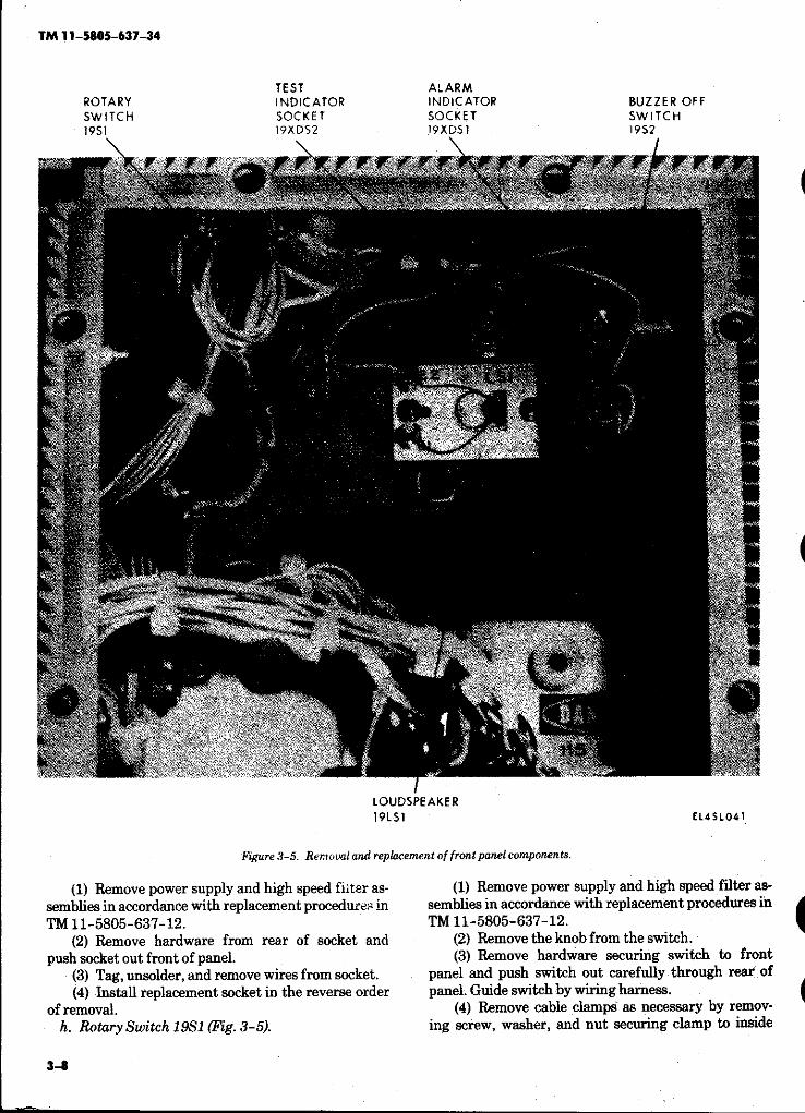


NOTEWhen installing new capacitors on filterCCA, secure capacitors to CCA with newstraps.(8) Install repaired filter CCA in the reverse order
of removal.(9) Replace power supply assembly in accordance
with replacement procedures in TM 11-5805-637-12.n. Transformer 19A1T1 (Fig. 3-7and 3-8).
(1) Remove power supply assembly in accordancewith replacement procedures in TM 11-5805-637-12.
(2) Remove three screws and washers from leftfront of power supply assembly securing front panelfilter CCA.
(3) Remove three screws and washers from rightfront of power supply assembly securing front panel tospacer bar.
(4) Remove front panel, with wires attached, andlay to one side.
(5) Remove four screws from bottom of powersupply.
(6) Remove transformer, with wires attached,through front of power supply assembly.
(7) Tag, unsolder, and remove wires from trans-former. Transfer the overvoltage absorber from pinsof removed transformer to the same pins on replace-ment transformer.
(8) Install replacement transformer in the reverseorder of removal.
(9) Replace power supply assembly in accordancewith replacement procedures in TM 11-5805-637-12.
o. Circuit Breaker 19A1CB1 (Fig. 3-6 and 3-7).(1) Remove power supply assembly in accordance
with replacement procedures in TM 11-5805-637-12.(2) Remove hardware securing circuit breaker to
front panel. Remove circuit breaker, with wires at-tached, through top of power supply assembly.
(3) Tag, unsolder, and remove wires from circuitbreaker.
(4) Install replacement circuit breaker in the re-verse order of removal.
(5) Replace power supply assembly in accordancewith replacement procedures in TM 11-5805-637-12.
p. POWER ON Indicator Socket 19A1XDS1 (Fig.3-7).
TM 11-5805-637-34
(1) Remove power supply assembly in accordancewith replacement procedures in TM 11-5805-637-12.
(2) Remove three screws and washers from leftfront of power supply assembly securing front panel tospacer bar and attached filter CCA.
(3) Remove three screws and washers from rightfront of power supply assembly securing front panel tospacer bar.
(4) Remove front panel, with wires attached, frompower supply assembly.
(5) Tag, unsolder, and remove wires from indi-cater socket.
(6) Remove hardware from rear of indicatorsocket and push socket out through front of frontpanel.
(7) Install replacement indicator socket in the re-verse order of removal.
(8) Replace power supply assembly in accordancewith replacement procedure in TM 11-5805-637-12.
q. Overvoltage Absorber 19A1RV1 (Fig. 3-7 and3-8).
(1) Remove diode bridge CCA in accordance withparagraph 3-10l.
(2) Unsolder and remove overvoltage absorberfrom transformer terminals 1 and 2.
(3) Install replacement overvoltage absorber inthe reverse order of removal.
(4) Replace power supply assembly in accordancewith replacement procedures in TM 11-5805-637-12.
r. Connector 19A1P1 (Figure 3-6).(1) Remove power supply assembly in accordance
with replacement procedures in TM 11-5805-637-12.(2) Remove two screws, washers, and nuts se-
curing the connector to the power supply. Remove con-nector, with wires attached, from power supply.
(3) Slide sleeving back from connector pins so thatwire/pin connections are exposed. Tag, unsolder, andremove wires from connector pins. Do not removesleeving.
(4) Install replacement connector in the reverseorder of removal, sliding sleeving back over pins afterwires are soldered on.
(5) Replace power supply assembly in accordancewith replacement procedures in TM 11-5805-637-12.
Section V. DiRECT SUPPORT TESTiNG PROCEDURES
3-11. Introduction 3-12. Operational TestTesting the data buffer at the direct support main- NOTEtenance level consists of performing the data buffer This tests only voice and relay functions ofoperational test. This test is used to verify proper data the data buffer. To insure proper data opera-buffer operation after the data buffer has been re- tion of data buffer, test unit in an operationalpaired. Failure of any of the operational test steps system to see if traffic passes through with-indicates a fault in the data buffer. When a fault is out errors.indicated, it maybe isolated by using the troubleshoot- To perform the data buffer operational test, proceed asing procedures in Section III of this chapter. follows:
3-11

TM 11-5805-637-34
Figures 3-8. Power supply assemblys, bottom view.
a. Set POWER switches on all equipment to OFF. channel (TD-1065/G output) should appear similar toConnect equipment as shown in figure FO-10. Set the waveform displayed on LEFT channel (TD - 1065/G in-TD-660 ( )/G MODE switch to the 12 CH position. put), but RIGHT channel peak-to-peak voltage should
b. Connect the oscilloscope and signal generator as be about 10% less than that of LEFT channel.indicated in table 3-3 for channel 1 testing. Set e. Repeat steps b through d for channels 2 throughPOWER switches on all equipment to ON. 12.
c. Adjust signal generator to produce output fre- f. Set POWER switch on data buffer to OFF.quency of 1 KHz at -4 dBm, using electronic voltmeter to g. Repeat steps b through e.observe signal level. h. Set POWER switches on all equipment to OFF.
d. The waveform displayed on RIGHT oscilloscope
3-12 CHANGE 2

TM 11-5805-637-34
Table 3-3. Connections for Data Buffer Operational Test
Section VI. OPERATIONAL TEST
3-13. Introductiona. The TS-3981 can be used to test the Data Buffer
TD-1065/G for errors, sync acquisition time, the alarmoperation. The same setup is used for all tests. Loopbacktesting is used The TD-1065( )/G must be operatedwith a Multiplexer TD-660A/G or TD-660B/G. TheTD-660/G cannot be used.
b. Audio test must be performed before power issupplied to the system.
NOTEExcept where indicated buffer data TD-660A/GMonnation referenced in this manual relates to theTD-660B/G as well.
3-14. Set-Up for Test Set Error Detector,and SG-1139/G Digital Data Generator
a. Interconnect the equipment shown in Figure 3-9when data generator or error detector is available.
b. Set controls of TD-660A/G units as follows(1) Master/Slave set to “Master”(2) Mode set to “12 CH”(3) 2 wire/4 wire set, to “4 wire”(4) “Aux” (In/out) set to “OUT”.
c. Turn on TD-660A/G unit and note the following(1) “Out of frame” indicator is extinguished.(2) All indicators are normal.
d. After opening the TD1065/G Circuit Card Assembly(CCA) access cover, set all 2 wire/4 wire switches on theChannel Unit CCAs (19A6) to the 4-wire position (UP).On Channel Unit CCA (19A6B) set A/B mode switch tothe A mode position (UP).
e. Apply power to the TB-1065/G and note the following(1) Initial alarm indicators (both audible and visual)
clear automatically. The audible alarm is silenced usingthe “BUZZER OFF” pushbutton switch on TD-1065/G.
(2) Note the status of the green “TEST” lamp on theTD-1065/G for the TEST SWITCH positions listed below:
GREEN “TEST” LAMPSWITCH POSITION INDICATION
OFF OFF-10V ON+10V ONXMT FRAME ONXMT TIME ONXMT PCM ONRCV PCM ONRCV TIME ONRCV FRAME ONCOM ONCHAN ON
(3) On the TD-660A/G units, note the following(a) “Out of frame” indicators are extinguished(b) All indicators are normal.
3-15. Operation When Using TS-3981/Por SG-1139/G
a. If TS-3981/P is used set the controls as followsfor the 32 kb/sec (4-wire test):(1) “PATTERN” Switch set to “LONG”.(2) “OPERATION” Switch set to “4W’(3) “CORRELATOR LOOP” Switch set to “OPEN”(4) “DATA” (ON/OFF) Switch set to “ON”.(5) “Rate Selection” Switch set to “7” (32 kb/s).(6) “Display Select” Switch set to “ERRORS”.
b. If using the SG-1139/G set the controls asfolIows:(I) “TIMING” to “MASTER”(2) “DATA RATE (kb/s)” to “32”.
Change 2 3-13

TM 11-5805-637-34
3-16 Testa. Energize the TS-3981/P or SG-139/G and
interconnect to Channel 1 of the TD-1065/G.NOTE
“DATA” (Activity) lamp on DSED(S)is/are lit (illuminated).b. Using the display “RESET” pushbut-
ton switch on the TS-3981/P or SG-1139/G, resetthe display to show no errors. Correlate datatransmission for errors for not less than five (5)seconds. Acceptance criteria will be no errorsshown on display. Rejection criteria will be whenany error(s) is/are shown on the display.
c. Using the “SINGLE ERROR” insertionpushbutton switch, inject errors (not less than ten(l0))into the data stream. Acceptance criteria willbe that the number of errors shown on the displayequal the number of errors inserted. Rejectioncriteria shall be that the number shown does notequal the number of errors inserted.
d. Set A/B mode switch on Channel UnitCCA (19A6B) to B position (down). Repeat stepsa thru c.
e. Repeat paragraph 3-15 steps a or b andparagraph 3-16 steps a-d for the remainingeleven (11) channels. This completes the 32kb/s4-wire tests.
f. TD-1065/G and TD-1065B/G with CCA19A6B in A mode only, for 16KB/s 4-wire testsuse figure 3-9. Set the “DATA” (RATE SELECT)Switch on the TS 3981/P to the “6” position (16kb/s) or data rate (kb/s) “SWITCH” on the SG-1139/G to “16”.
g. Interconnect the TS-3981/P or SG-1139/Gto Channel 1 of the TD-1065/G or TD-1065B/G.
NOTE“Data” (activity) indicator on the SED(UNIT B) is “on”.h. Using the display “RESET” pushbutton
switch on the TS-3981/P or SG-1139/G, reset thedisplay to show no errors. Correlate data trans-missions for errors for not less than five (5) sec-onds. Acceptance criteria will be no errors shownon display(s). Rejection criteria will be when anyerror(s) is/are shown on the display(s).
i. Using the “SINGLE ERROR” insert push-button switch on the DSED(S), inject errors (notless than ten (10)) into the data stream. Accep-tance criteria shall be that the number of errorsdisplayed equal the number inserted.
j. Repeat paragraph 3-16 steps f, g, h, and ifor the remaining eleven (11) channels.3-17 161kb/s 2-wire Tests, TD-106S ( )/Q
a. Connect as shown in figure 3-10.h Set 2W/4W Switches on CCA 19A6, CCA
19A6A or CCA 19A6B card to 2W position(down).On Channel Unit CCA 19A6B A/B modeSWITCH to A mode position (up).
c Interconnect TS-3981/P or SG-1139/G tochannel 1 of the TD-1065 ( )/G controls on bothdrop boxes to channel 1.
d. Observe the “data” activity indicator. Ac-ceptance criteria shall be that the activity indi-cator is lit or flashing. Rejection criteria shall bethat the activity indicator is off.
e. Set A/B mode switch on Channel Unit CCA(19A6B) to B position (down). Repeat step d.
f. Repeat paragraph 3-17 steps a thru e forthe remaining 11 channels. This completes the16kb/sec-2 wire testing.
3-14 Change 2

Figure 3-9.
TM
1
1-5
80
5-6
37
-34
Change 2
3-1
5

Figure 3-10.
TM
11
-58
05
-63
7-3
4
3-1
6C
hange 2

TM 11-5805-637-34
CHAPTER 4
GENERAL SUPPORT MAINTENANCE INSTRUCTIONS
The direct support maintenance instructions contained in Chapter 3 of this manual are applicable to general sup-port maintenance.
4-1

TM 11-5805-637-34
APPENDIX A
REFERENCES
DA Pam 25-30DA Pam 738-750TM 11-5805-637-12
TM 11-5805-637-2ZP
TM 11-5805-637-34P
TM 11-6625-654-14
TM 11-6625-683-15
TM 11-6625-2658-14
TB 43-0118
TM 740-90-1TM 750-244-2
Consolidated Index of Army Publications and Blank Forms.The Army Maintenance Management System (TAMMS).Operator and Organizational Maintenance Manual, Buffer, Data TD-1065/G
(NSN 58054)14)28-8364).Organizational Maintenance Repair Parts and Special Tools Lists for Data Buffer
TD-1065/G (NSN 5805-01-028-8364).Direct Support and General Support Maintenance Repair Parts and Special Tools
List (Including Depot Maintenance Repair Parts and Special Tools) for DataBuffer TD-1065/G (NSN 5805-01-028-8364).
Operator’s, Organizational, Direct Support and General Support MaintenanceRepair Parts and Special Tools List (Including Depot Maintenance RepairParts and Special Tools List) for Multimeter, AN/USM-223.
Operator’s, Organizational, Direct Support, General Support, and DepotMaintenance Manual Signal Generator AN/URM-127 (NSN 6625-00-783-5965).
Operator’s, Organizational, Direct Support and General Support MaintenanceManual for Oscilloscope, AN/USM-281C (NSN 6625-00-106-9622).
Field Instructions for Painting and Preserving Electronics Command EquipmentIncluding Camouflage Pattern Painting of Electrical Equipment Shelter.
Administrative Storage of Equipment.Procedures for Destruction of Electronics Materiel to Prevent Enemy Use
(Electronics Command).
Change 2 A-1/(A-2 blank)

TM11-5805-637-34
APPENDIX B
REPAIR PARTS AND SPECIAL TOOLS LISTS
Refer to TM 11-5805-637-34P for repair parts and special tools list.
B-1

TM 11-5805-637-34
Data buffer, overall block diagram.Figure FO-1.

TM 11-5805-637-34
Figure FO-2. TD-660( )/G frame format, six and 12-channel.

TM 11-5805-637-34
Figure FO-3. Fault locator CCA 19A3, functional block diagram

TM 11-5805-637-34
Figure FO-4. Transmit common CCA 19A4 (input/select section), functional block diagram.

TM 11-5895-637-34TO 31S5-2G-272
Figure FO-5. Combining channel process timing, six and 12-channel.

TM 11-5805-637-34
Figure FO-6. Transmit common CCA 19A4 (output/timing section), functional block diagram.

TM 11-5805-637-34
Figure FO-7. Receive common CCA 19A5, functional block diagram.

0 T M 1 1 - 5 8 0 5 - 6 3 7 - 3 4T O 0 3 1 S 5 - 2 G - 2 7 2
CHANGE 1Figure FO-8. Channel CCA 1GA6 and CC19A6A (transmit section), functional block diagram.

Figure FO-9.
TM 11-5805-637-34

Figure FO-10
TM 11-5805-637-34TO 31S5-2G-272
CHANGE 1

TM 11-5805-637-34
Figure FO-11. Power supply 19A1, schematic diagram.

TM 11-5808-637-34
Figure FO-12. Power supply 19A1, wiring diagram.


TM 11-5805-637-34
Figure FO-14. Standard color coding chart.

By Order of the Secretary of the Army:
Official:J. C. PENNINGTON
Major General, United States ArmyThe Adjutant General
DISTRIBUTION:Active Army:
HISA (Ft Monmouth) (21)USAINSCOM (2)COE(l)TSG(l)USAARENBD (1)DARCOM (1)TRADOC (2)OS Maj Comd (4)TECOM (2)USACC (4)MDW(l)Armies (2)Corps (2)Svc Colleges (1)USASIGS (5)USAADS (2)USAFAS (2)USAARMS (2)USAIS (2)USAES (2)USAICS (3)MAAG (1)USARMIS (1)USAERDAA (1)USAERDAW (l)Fort Gordon (10)Fort Carson (5)Army Dep (1) except
SAAD (30)TOAD (14)SHAD (2)
Fort Gillem (10)USA Dep (1)Sig Sec USA Dep (1)Fort Richardson (CERCOM Ofc) (2)Units org under fol TOE:
(2 copies each unit)29-20729-610
ARNG: NoneUSAR: NoneFor explanation of abbreviations used, see AR 310-50.
E. C. MEYERGeneral, United States Army
Chief of Staff
* U.S. GOVERNMENT PRINTING OFFICE: 1990 - 261-872 (20847)


THE METRIC SYSTEM AND EQUIVALENTS

P I N : 0 4 8 3 7 4 - 0 0 2