TBMVN1de1.pdf - UPCommons
122
“NOVEL METAL INSULATOR METAL CAPACITORS BASED ON ELECTROSPRAYED COLLOIDAL NANOPARTICLES ” Thesis submitted as a compendium of publications in partial fulfillment of the requirement for the PhD Degree issued by the Universitat Politècnica de Catalunya, in its Electronic Engineering Program. Bremnen Marino Véliz Noboa Supervisor: Alexandra Bermejo Broto Barcelona, 2019 Electronic Engineering Department
-
Upload
khangminh22 -
Category
Documents
-
view
3 -
download
0
Transcript of TBMVN1de1.pdf - UPCommons

“NOVEL METAL INSULATOR METAL CAPACITORS BASED ON ELECTROSPRAYED COLLOIDAL
NANOPARTICLES ”
Thesis submitted as a compendium of
publications in partial fulfillment of the
requirement for the PhD Degree issued
by the Universitat Politècnica de
Catalunya, in its Electronic Engineering
Program.
Bremnen Marino Véliz Noboa
Supervisor: Alexandra Bermejo Broto
Barcelona, 2019
Electronic Engineering Department

2
To my family and to God for blessing my family

3
Abstract
This work develops a novel capacitor device based on the use of nanotechnology. The
device starts from the exiting metal-insulator-metal (MIM) concept, but instead of a
continuous insulator layer, dielectric nanoparticles are used. Nanoparticles are mainly of
silicon oxide (silica) and polystyrene (PS) and the diameter values are 255nm and 295nm
respectively. The nanoparticles contribute to a very high surface to volume ratio and are
easily available at low cost. The deposition technology developed in this work is based
on the use of the electrospray technique, which is a bottom-up fabrication technology that
allows batch processing and achieves a good compromise between large area and low
deposition time. With the objective of increasing the deposit surface, the electrospray set-
up has been tuned to allow deposition areas from 1cm2 to 25cm2.
The fabricated devices, the so called nanoparticles metal insulator metal (NP-MIM)
capacitors, offer higher capacitance values than a similar conventional capacitor with a
continuous insulator layer. In the case of silica NP-MIMs, a factor as high as 1000 of
capacitance enhancement is achieved, whereas polystyrene NP-MIMs exhibit capacitance
gains in the range of 11. In addition, silica NP-MIMs show capacitive behaviours in a
specific frequency ranges which depends on the humidity and thickness of the
nanoparticles layers thickness, while polystyrene NP-MIMs always maintain their
capacitive behaviour.
The fabricated devices have been characterized by scanning electron microscopy (SEM)
measurements complemented with focusing ion beam (FIB) drilling to characterise the
topography of the NP-MIMs. The devices have also been characterized by impedance
spectroscopy measurements, at different temperatures and humidifies. The origin of the
enhanced capacitance is associated in part to humidity in the nanoparticles interfaces. A
circuital model based on distributed elements has been developed to fit and predict the
electrical behaviour of the NP-MIMs.
In summary, this thesis shows the design, fabrication, characterization and modelling of
a new promising nanoparticles metal-insulator-metal capacitor that may pave the way to
the development of a novel MIM-supercapacitor technology.

4
Resumen
Este trabajo desarrolla un novedoso dispositivo condensador basado en el uso de la
nanotecnología. El dispositivo parte del concepto existente de metal-aislador-metal
(MIM), pero en lugar de una capa aislante continua, se utilizan nanopartículas
dieléctricas. Las nanopartículas son principalmente de óxido de silicio (sílice) y
poliestireno (PS) y los valores de diámetro son 255nm y 295nm respectivamente. Las
nanopartículas contribuyen a una alta relación superficie/volumen y están fácilmente
disponibles a bajo costo. La tecnología de depósito desarrollada en este trabajo se basa en
la técnica de electrospray, que es una tecnología de fabricación ascendente (bottom-up)
que permite el procesamiento por lotes y logra un buen compromiso entre una gran
superficie y un bajo tiempo de depósito. Con el objetivo de aumentar la superficie de
depósito, la configuración de electrospray ha sido ajustada para permitir áreas de depósito
de 1cm2 a 25cm2.
El dispositivo fabricado, los llamados condensadores de metal aislante de nanopartículas
(NP-MIM) ofrecen valores de capacidad más altos que un condensador convencional
similar con una capa aislante continua. En el caso de los NP-MIM de sílice, se alcanza un
factor de hasta 1000 de mejora de la capacidad, mientras que los NP-MIM de poliestireno
exhibe una ganancia de capacidad en el rango de 11. Además, los NP-MIM de sílice
muestran comportamientos capacitivos en específicos rangos de frecuencias que depende
de la humedad y el grosor de la capa de nanopartículas, mientras que los NP-MIM de
poliestireno siempre mantienen su comportamiento capacitivo.
Los dispositivos fabricados se han caracterizado mediante medidas de microscopía
electrónica de barrido (SEM) complementadas con perforaciones de haz de iones
focalizados (FIB) para caracterizar la topografía de los NP-MIMs. Los dispositivos
también se han caracterizado por medidas de espectroscopia de impedancia, a diferentes
temperaturas y humedades. El origen de la capacitancia aumentada está asociado en parte
a la humedad en las interfaces de las nanopartículas. Se ha desarrollado un modelo de un
circuito basado en elementos distribuidos para ajustar y predecir el comportamiento
eléctrico de los NP-MIMs.
En resumen, esta tesis muestra el diseño, fabricación, caracterización y modelización de
un nuevo y prometedor condensador nanopartículas metal-aislante-metal que puede abrir
el camino al desarrollo de una nueva tecnología de supercondensadores MIM.

5
Acknowledgments
Fist at all, I would like to take the opportunity to express my sincere gratitude to
Alexandra Bermejo, for the trust placed in me as a doctoral student. I am grateful for her
valuable guidance, as well as her continues support though the course of this thesis. Under
her supervision I have learned a lot.
I would like to say thank to Albert Orpella for his estimable collaboration when I needed
support. A special thanks to Luis Castañer for sharing his knowledge and experience.
I would like to thank to Gema Lopez, Arnau Coll and the clean room technical staff for
the training and support in the management of the different instruments and laboratory
equipment. Thanks to Jordi Vives co-author of one of the articles presented here, and
thanks to the rest of my colleagues that in one way or another accompanied during the
development of this thesis.
Last but not least, I would like thank to all member of my family, to my father for his
advice and encouragement, and an exceptional gratitude to my wife and my children for
their company, unconditional love and the great effort involved during these last years.

6
Peace is not just the absence of war. Peace is above all the presence of justice, health,
education, social security, decent salaries, basic needs satisfied.
The insulting opulence next to the most intolerable poverty, are also daily bullets
against human dignity.
Rafael Correa, former Ecuadorian president.

7
Contents
Abstract ............................................................................................................................. 3
Resumen ........................................................................................................................... 4
Acknowledgments ............................................................................................................ 5
List of Figures ................................................................................................................... 9
List of Tables .................................................................................................................. 12
CHAPTER I Introduction .............................................................................................. 13
1.1. Context ............................................................................................................. 13
1.2. Thesis structure ................................................................................................ 14
1.3. Objectives ........................................................................................................ 15
Main objective ........................................................................................................ 15
Specific objectives .................................................................................................. 15
1.4. Design .............................................................................................................. 15
1.5. Journals papers ................................................................................................. 19
1.6. Characterization Methods ................................................................................ 20
1.7. References ........................................................................................................ 28
CHAPTER II Thesis Background ................................................................................. 32
2.1. MIM capacitors ................................................................................................... 32
2.1.1. Planar-MIMs. ................................................................................................ 32
2.1.2. Three-dimensional-MIMs ............................................................................. 36
2.2. Supercapacitors .................................................................................................... 41
2.2.1. Supercapacitor concept ................................................................................. 41
2.2.2. Supercapacitors classification....................................................................... 45
2.2.3. Advances in Electrical Double Layer capacitors .......................................... 47
CHAPTER III Compendium of papers .......................................................................... 70

8
3.1. Paper #1: Impedance modelling of silica nanoparticle metal insulator metal
capacitors. ................................................................................................................... 70
3.2. Paper #2: Capacitive study of a polystyrene nanoparticles capacitor using
impedance spectroscopy. ............................................................................................ 80
3.3. Paper #3: Large area deposition of ordered nanoparticle layers by electrospray. 89
CHAPTER IV Discussion ............................................................................................. 96
4.1. Electrospray deposition conditions of NP-MIMs. ............................................... 96
4.2. High capacitance of NP-MIM capacitors ............................................................ 97
4.3. NP-MIMs modelling. ........................................................................................ 101
4.5. Scaling-up of NP-MIMs deposition area by electrospray technique ................. 104
CHAPTER V Conclusions and future works ............................................................... 106
Conclusions .............................................................................................................. 106
Future works ............................................................................................................. 108
Appendices ................................................................................................................... 109
Appendix A Electrospray and nanoparticles specifications .................................... 110
Appendix B. Impedance spectroscopy of others NP-MIM capacitors at controlled
environment conditions ............................................................................................ 112
Appendix C. Obtaining the transient response. ....................................................... 117
Appendix D Conference publications ...................................................................... 121
Appendix E Thesis related projects ......................................................................... 122

9
List of Figures
Figure 1. (a) Nanoparticles Metal-Insulator-Metal structure schema, (b) equivalent
conventional Meta-Insulator-Metal schema. .................................................................. 17
Figure 2. Schematic of how the colloidal nanoparticles are deposited by an electrospray
system. ............................................................................................................................ 18
Figure 3. Designed masks used for the photolithography process in the fabrication of NP-
MIM structures. .............................................................................................................. 18
Figure 4. Ideal capacitor and its Nyquist plot. C=60µF, R=100Ω ................................ 23
Figure 5. Simplified Randle Circuit and its Nyquist plot. C=60µF, R=100Ω, Rs=20 Ω.
........................................................................................................................................ 24
Figure 6. Randle circuit and its Nyquist plot. C=60µF, R=100Ω, Rs=20 Ω, Aw=20
Ω(jw)1/2 ........................................................................................................................... 25
Figure 7. Voigt circuit model. ....................................................................................... 26
Figure 8. (a) Image of the SEM microscope of the UPC Multiscale facility, (b) SEM
image of monodisperse nanoparticles (C) SEM images of nanoparticles of two sizes. . 27
Figure 9. Schematic of an integrated MIM capacitor. ................................................... 32
Figure 10. (a) Schematic of a Al2O3/ZrO2/Al2O3 MIM capacitor, (b) Schematic of the
microwave chamber for post-deposition annealing, (c) TEM picture (source [18]). .... 35
Figure 11. (Left) Diagram of the triple layer stack MIM capacitor, (right) schematic of
the triple layer stack MIM capacitor in 3-D doped silicon substrate. Source [26]. ........ 36
Figure 12. (a) Cross-sectional TEM image of a AlZnO/Al2O3/AlZnO MIM capacitor with
anodic aluminum oxide (AAO) nanopores, (b) Schematic of atomic layer deposition of
the AlZnO/Al2O3/AlZnO and (c) final schematic of the 3D AlZnO/Al2O3/AlZnO MIM
capacitor [27]. ................................................................................................................. 37
Figure 13. Cross-sectional TEM images of AlZnO/Al2O3/AlZnO MIM capacitors based
on ZnO nanowires with (a) 5nm and (b) 20nm Al2O3 dielectric layers, (c) and (d)
magnified cross-sectional TEM images of 3D-MIM capacitor with 5nm and 20nm
respectively. Source [30]. ............................................................................................... 38
Figure 14. (a) Schematic of a three-dimensional nanoscale interdigitated electrodes
capacitor, (b) Interdigital AAO template [31]. ............................................................... 39
Figure 15. SEM cross-section of the bottom of the nano-tubular MIM. The Al2O3
template barrier with the ALD TiN electrodes and the ALD Al2O3 layer is observed
(source [32]). .................................................................................................................. 39

10
Figure 16. Examples of systems where SCs are found: trams (Barcelona), hydride cars
(Toyota) and uninterruptible power supplies.................................................................. 41
Figure 17. Supercapacitors marked forecast (source [36]). ........................................... 42
Figure 18. Schematic of a supercapacitor including the anode, cathode, electrolyte and
the electrical double layers. ............................................................................................ 43
Figure 19. Classification of supercapacitors: The Electrical Double Layer, Pseudo and
Hybrid Capacitors. .......................................................................................................... 46
Figure 20. Specific capacitance of active materials in supercapacitors (source [44]). .. 46
Figure 21. Diagram of the fabrication process of activated carbon............................... 47
Figure 22. SEM images of activated carbon electrodes extracted (a) from a specific
fabricated electrodes and (b) a commercial one (source [50]). .................................. 49
Figure 23. Inverse opal carbon template: (a) Fabrication steps (b) SEM image (source
[51]). ............................................................................................................................... 49
Figure 24. A SEM image of the surface of carbide derived carbon synthetized from TiC.
(source [52]). .................................................................................................................. 50
Figure 25. SEM images of randomly entangled and cross-linked SWNT (source [61]).
........................................................................................................................................ 51
Figure 26. TEM image of randomly entangled and cross-liked MWNTs with an average
diameter of 8nm (source:[62]). ....................................................................................... 52
Figure 27. SEM pictures of different CNT arrangements: (a) curly and non-aligned CNTs
using thermal CVD, (b) vertical aligned CNTs using PECVD (source [67]). ............... 53
Figure 28. SWNT forest synthesized with water assisted CVD (source [71]). ............. 53
Figure 29. Schematic illustration of the fabrication of the PANI/VA-CNTs electrodes
(source [72] ). ................................................................................................................. 54
Figure 30. Images of a (a) flexible graphene supercapacitor (source [79]) on PET
substrate. Schematic of another (b) flexible graphene supercapacitor (source [80]) on
paper substrate. ............................................................................................................... 55
Figure 31. SEM image of RG-O platelets obtained by heating graphene oxide in PC
(source [81] ). ................................................................................................................. 56
Figure 32. Schematic of the fabrication process of C-RGO from GO solution using
electrospray technique. C-GO is reduced in the hydrazine hydrate vapour at 85 °C, source
[82]. ................................................................................................................................ 56
Figure 33. Schematic of the fabrication of a RGO electrode. (source [84]).................. 57

11
Figure 34. Capacitance behaviour of the NP MIM capacitors versus frequency at room
temperature. .................................................................................................................... 99
Figure 35. Capacitance versus frequency at different temperature for silica NP MIM D.
...................................................................................................................................... 100
Figure 36. Capacitance versus frequency at different temperature for polystyrene NP
MIM. ............................................................................................................................. 100
Figure 37. Electrospray system mounted in the UPC facilities. .................................. 110
Figure 38. Capacitance versus frequency plot for the Silica NP-MIM E, at 25ºC, for
different Relative Humidity (RH) values. .................................................................... 112
Figure 39. Capacitance versus frequency plot for the Polystyrene NP-MIM 2, at 25ºC,
for different Relative Humidity (RH) values. ............................................................... 113
Figure 40. Modified Randles circuit used to model silica NP-MIM E and polystyrene
NP-MIM 2. ................................................................................................................... 113
Figure 41. Nyquist plot measured for silica NP-MIM E at different relatively humidity
and a temperature of 25ºC. The frequency scan starts at 0.1Hz. .................................. 114
Figure 42. Nyquist plot measured for polystyrene NP-MIM 2 at different relative
humidity and a temperature of 25ºC. The frequency scan starts at 1Hz. ..................... 114
Figure 43. Normalized Power for the silica NP-MIM E sample at 90 and 40 % relative
humidity (RH): Active power P/|S| and reactive power Q/|S|. The crossing point shifts to
the left. .......................................................................................................................... 115
Figure 44. Normalized Powers at different relative humidity for the polystyrene NP-MIM
2 sample: Active power P/|S| and reactive power Q/|S|. There is not crossing point. .. 116

12
List of Tables
Table 1. Basic modelling elements used in electrical impedance spectroscopy ............ 22
Table 2. Main characteristics of dielectric materials [6] [12] [13]. ................................ 34
Table 3. Comparison of main characteristic of relevant MIM capacitors [17]. ............. 35
Table 4. Comparison of different 3D MIM capacitors technologies .............................. 40
Table 5. Comparison of capacitors, supercapacitors and batteries (source [35]). .......... 42
Table 6. Some available commercial SCs and characteristics (source: [37]). ............... 44
Table 7. Comparison of different carbon based electrode materials used in EDLCs. .... 58
Table 8. Areal capacitance and double layer capacitance of carbon materials .............. 58
Table 9. Summary of areal capacitance, gravimetric capacitance and capacitance gain of
the reported NP-MIMs. .................................................................................................. 98
Table 10. Summary of electrospray conditions used for the nanoparticle deposition in the
NP MIM ........................................................................................................................ 111
Table 11. Fitting elements for the silica NP-MIM E capacitor at 90%RH, 70%RH,
50%RH and 40%RH. .................................................................................................... 115
Table 12. Fitting elements for the polystyrene NP-MIM 2 capacitor at 90%RH, 60%RH
and 40%RH. ................................................................................................................. 115

13
CHAPTER I
Introduction
1.1. Context
Nanoparticles are irrupting in the day-by-day, many consumer products are made of
nanoparticles in order to benefit our daily life [1], for instance silver nanoparticles are
used in shampoos and detergents, or zinc oxide nanoparticles in sunscreens. Silicon oxide
nanoparticles are used as an anti-caking agent to increase the taste value and prolong the
shelf-life of food, fumed silica oxide nanoparticles are used in toothpastes and cosmetics
as a light abrasive additive. Within the energy storage research area, the inclusion of
carbon nanotubes, graphene, transition metal oxide, silicon and silica nanoparticles as
active material in electrodes, are improving the performance of the supercapacitors [2]
[3] [4] and lithium batteries [5] [6].
The revolutionary growing of the technologies at the nanoscale has allowed the synthesis,
manipulation and characterization of different kind of nanoparticles and in turn the
fabrication of novel nanostructures. On one hand, the fabrication of nanostructures has
been dominated by top-down [7] approaches as a legacy of the semiconductor industry,
thus various new, but expensive nanolithographic techniques [8] such as electron beam
lithography, x-ray lithography, scanning probe lithography and nanoimprinting have
emerged to improve the pattering resolution at the nanometre scale. On the other hand,
bottom-up assembly approaches, where the nanostructures are self-assembled from
smaller pieces, are pretty cheaper and faster than top-down assembly approaches [9]. In
many applications, such as the ones within the photonic research field, monodisperse
nanoparticles are used to make periodic and ordered nanostructures termed as colloidal
crystals (opals and inverse opal) self-assembled by bottom-up methods such as drop
casting [10] [11], vertical deposition [12], spin-coating [13], dip-coating [14], shear
ordering [15], Lagmuir-blodgett [16] and electrospray techniques among others [17].
Due to the low cost and simplicity of the electrospray technique, the MNT group has
developed a specific set-up using this technology as an innovative method to self-

14
assemble silica [18] and polystyrene [19] nanoparticles in order to fabricate metamaterials
[20]. However, as far as we know, similar nanostructures have not been reported yet for
energy store applications. It is in this context when it comes down to the idea of using
dielectric nanospheres instead of a continuous dielectric film as an insulating layer to
fabricate Metal Insulator Metal (MIM) capacitors. Preliminary evidence based on
impedance spectroscopy characterisation suggested that in this new type of MIM
capacitor, the effect of using these nanospheres may cause an increase on the expected
capacitance for an equivalent conventional MIM capacitor with continuous dielectric
layer of same dimensions, signifying that these new devices are promising for its use as
supercapacitors [21].
Thereby, the main aim of this PhD work is to explore an alternative Metal-Insulator-Metal
(MIM) device using electrosprayed dielectric nanoparticles for energy store applications.
Design and fabrication of the MIM capacitor is carried out using different dielectric
nanoparticles materials, mainly monodisperse silicon oxide and polystyrene nanospheres.
This work shows a compressive analysis of the MIM capacitor using impedance
spectroscopy characterisation to model the physics in the interfaces of the MIM and the
physical phenomena of electrical double layer that could be present in the nanospheres
interfaces.
1.2. Thesis structure
This thesis is presented as a compendium of papers published in recognized international
journals in the field of nanotechnology and electrochemistry. The document is structured
into five charters. The first chapter is the introduction of the thesis including the main
goals, the design of the capacitors and the experimental characterization methods.
Chapter 2 shows the state of the art, focused on high specific capacitance MIM capacitors
and supercapacitors. As it will be seen later, impedance spectroscopy equivalent circuit
usually employed to model supercapacitors resulted suitable to model the nanoparticles
metal-insulator-metal (NP-MIM) capacitors shown in this thesis.
Chapter 3 contains the full text of the three publications and Chapter 4 the global
discussion of the results and main performance parameters following to the set goals.

15
Chapter 5 shows the conclusions derived from this thesis and the potential future lines of
research. Finally, the appendix includes conference publications and complementary
information that has not been published yet, but are relevant to the thesis.
1.3. Objectives
Main objective
The purpose of this thesis is to research on the understanding and fabrication of
nanoparticles based Metal-Insulator-Metal (NP-MIM) structures using electrosprayed
dielectric nanospheres as the insulator layer, exploring the performance by impedance
spectroscopy characteristics to analyse its use as an alternative energy store device.
Specific objectives
Design and fabrication of NP-MIM capacitors, where the insulator layer is
deposited by electrospraying of monodisperse dielectric nanoparticles, mainly
silicon oxide and polystyrene materials.
Impedance spectroscopy characterization and modelling of the NP-MIM
structures.
Analyse the use of theses NP-MIM capacitors as energy store devices.
Scaling-up of the nanoparticles based structures deposition area using
electrospray technique.
Analyse the possibility of using these NP-MIM capacitors as humidity sensors.
1.4. Design
Figure.1a shows a generic schema of the nanoparticles metal insulator metal (NP-MIM)
structure. Figure.1b shows the hypothetical conventional equivalent (same dimensions)
MIM capacitor with a continuous insulator layer.
Aluminium layers were employed both as bottom electrode and top electrode using
microelectronic standard fabrication process steps. Electrospray technique is used to

16
deposit the nanoparticles by means of a high voltage between the bottom electrode and a
needle that acts as nanoparticle gun. This fabrication process steps are the following:
A. Clean the glass microscope slide substrate sequentially with acetone, propanol,
deionized water and nitrogen to remove dust or any residual contaminant from the
surface.
B. Pour on the glass substrate surface the SPR 220-7 photoresist and to spin it in
order to obtain a 7µm thick photoresist film.
C. Post-bake process to remove the excess solvent in order to dry and stabilize the
photoresist film.
D. Expose with ultraviolet light the photoresist through a mask (nano-MIM2 base
mask) which contains the pattern of the bottom electrodes and paths.
E. Develop the photoresist using a MF24 solution to remove the exposed photoresist.
F. Deposit an aluminium layer on the sample using thermal evaporation deposition.
G. Definition of the bottom aluminium layout on the glass substrate by a lift-off
process.
H. A new photoresist film is spun coated on the sample surface.
I. New lithography process (nano-MIM2 pous mask) and development are
performed to open two windows in the photoresist, one window for the NP-MIM
structure and the other window for the electrical connection with the bottom
electrode.
J. The nanoparticles are electrosprayed on the corresponding opened window on the
bottom electrode.
K. Finally, the top electrode is a thin aluminium film deposited onto the nanoparticles
and onto the photoresist layer using a shadow mask.

17
Figure 1. (a) Nanoparticles Metal-Insulator-Metal structure schema, (b) equivalent conventional
Meta-Insulator-Metal schema.
Electrospray deposition method is a low cost, rapid and simple technique that can work
at room temperature. The electrospray system consists on an infusion pump, a
microfluidic tube, a needle, a high voltage source and a digital camera, as it is observed
in Figure 2. The nanoparticle suspension contained in a syringe is pressed at a constant
flow by the infusion pump, then the suspension travels through the fluidic microchannel
to the positively polarized needle, where the suspension is electrosprayed focusing the
nanoparticles on the substrate. The surface substrate is connected to the negative terminal
of the high voltage source. A digital camera inspects the formation of the cone of Taylor
in the needle tip. Taylor cone is stable shape created between the capillary and the jet
region when the potential difference reaches a threshold value.

18
Figure 2. Schematic of how the colloidal nanoparticles are deposited by an electrospray system.
Three individual masks are used in the NP-MIM structure fabrication; each mask
containing eight samples, that contains three NP-MIM structures as the same time. The
first mask (Figure 3b) is designed to fabricate the bottom electrode. The second mask,
(Figure 3a) patterns the photoresist, and the last mask (Figure 3c) is the shadow mask
used for top electrode metal deposition. The NP-MIM fabrication may potentially avoid
any photolithography steps, by using shadow masks, thus decreasing the cost of the final
device.
Figure 3. Designed masks used for the photolithography process in the fabrication of NP-MIM
structures.

19
1.5. Journals papers
The following papers form part of the compendium of publications according to the goals
of this thesis.
1.5.1. Paper #1
Paper [22] entitled: “Impedance modelling of silica nanoparticle metal insulator metal
capacitors”. Published in Electrochimica Acta.
Brief description: “In this paper, some silica NP MIM capacitors are fabricated with 255
nm diameter silica nanospheres as insulator layer using electrospray technique, resulting
in an enhanced capacitance (up to 1000) compared to a conventional planar configuration.
The capacitance enhancement is found to be associated to charge in the nanoparticle
interfaces. Besides, an in-depth study of electrochemical impedance spectroscopy
modelling and charge-discharge transients is provided. Impedance spectroscopy
measurements fitted very well with a Randles equivalent circuit formed by sub-circuits
that describes the nanoparticles and the nanoparticle-metal interfaces. Maltab simulations
prove that the charge-discharge transient measurements perfectly agree with the Randles
equivalent circuit.”
1.5.2. Paper #2
Paper [23] entitled: “Capacitance study of a polystyrene nanoparticle capacitor using
impedance spectroscopy”. Published in Nanotechnology.
Brief Description: In this paper, a polystyrene NP MIM capacitor is fabricated with
295nm diameter polystyrene nanoparticles as insulator layer using electrospray
technique. Measured capacitance values are up to 11.7 larger than the expected for a
conventional metal insulator metal capacitor of planar geometry and continuous
polystyrene layer calculated with the classic formula. Electrochemical impedance
spectroscopy modelling showed the deterioration of the metal-nanoparticles interfaces
and a slight decrease in the capacitance with the temperature increase which is associated
to charges localized at the nanoparticles interfaces due to the environmental humidity.

20
1.5.3. Paper #3
Paper [24] entitled: “Large area deposition of ordered nanoparticle layers by
electrospray”. Published in Colloid and Interface Science Communications.
Brief description: In this paper, the deposition area scaling-up of the nanoparticle based
structures is performed. Two approaches are implemented using the electrospray
technique. An area of 25 cm2 is achieved using an electrospray system formed by an array
of four needles, while up to 7.5 cm2 areas are achieved by using a guard ring electrode
placed in the electrospray jet trajectory. COMSOL simulations of the electric field
distribution are carried out by the two electrospray configurations.
1.6. Characterization Methods
In this thesis, two characterizations methods have been mainly used:
Electrical Impedance Spectroscopy (EIS) characterization was carried out to analyses the
electrical behaviour of the NP-MIM capacitors in different frequency ranges. The HIOKI
IM3590 impedance analyser and the Agilent 4294A impedance analyser have been used
for this purpose.
Scanning electron microscopy (SEM) and Focused Ion Beam (FIB) characterization was
used to determine the nanoparticles diameters, the orography and the thickness of the
nanoparticles layers. The SEM microscopy used was the ZEIS NEON 40.
1.6.1. Electrical Impedance Spectroscopy (EIS)
There are many impedance measurement methods [25] such as bridge method, I-V
method, network analysis method or auto-balancing bridge method. The last one is the
used because it owns wide frequency coverage with high accuracy. Electrical impedance
spectroscopy [26] is the most used characterisation tool in electrochemical materials and
devices analysis. All methods are based on the measurement of an alternating current Ĩ
resulted from the application of a small sinusoidal wave potential Ṽ at a wide range of
frequencies.

21
𝑍 =Ṽ
Ĩ= |𝑍|(cos 𝜃 + jsin 𝜃) ( 1 )
Where |Z| and θ are the module and phase of the impedance and they are dependent on
the frequency. The real and the imaginary impedance components, Z' and Z’’ are depicted
by the equations (2) and (3):
𝑍′ = |𝑍| cos 𝜃 ( 2 )
𝑍′′ = |𝑍| sin 𝜃 ( 3 )
The admittance can be calculated from Z as (4):
𝑌 =1
𝑍= 𝑌′ + 𝑗𝑌′′ ( 4 )
The values of |Z|, θ, Z', Z'', Y' and Y'' data can be acquired by an impedance analyser
including the established frequency range.
The complex capacitance [27] [28] depends on the angular frequency and it is defined as
(5):
𝐶∗ =1
𝑗𝜔𝑍= 𝐶′ + 𝑗𝐶′′ = −
𝑍′′
𝜔|𝑍|2+ 𝑗
𝑍′
𝜔|𝑍|2 ( 5 )
Where C’ is the real capacitance or simply termed as capacitance, corresponds to the one
measured by constant charge-discharge current. For a MIM structure of parallel plates
configuration, C’ defined as (6):
𝐶′ = 𝜖𝐴
𝑑= −
𝑍′′
𝜔|𝑍|2 ( 6 )
Where A is the electrode area, d is the dielectric thickness (or separation between the
parallel plates), and ϵ is the dielectric permittivity of the dielectric.
The Imaginary Capacitance C’’ (5) is related to the energy dissipation including both
dielectric loss and conductivity.
Other useful equations are the normalized powers respect to the apparent power defined
as:

22
𝑃 |𝑆| = cos 𝜃 =𝑍′ |𝑍|⁄⁄ ( 7 )
𝑄 |𝑆| = sen 𝜃 =𝑍′′ |𝑍|⁄⁄ ( 8 )
1.6.2. Impedance modelling
The usual modelling elements used in electrical impedance spectroscopy are: Resistor R,
Capacitance C, Constant Phase element (CPE) [29] and Warburg element W [30].
The resistor is usually a charge transfer resistor (also named polarization resistance) that
is the resistance of the electrons through an interface (as electrode-electrolyte) occurred
when a voltage is applied. The capacitance states for a double layer capacitance that is
the space charge stored at an interface when applying a voltage. A constant phase element
is a frequency dependent element associated to a distributed capacitance (as a double
layer capacitance) due to a non-uniform potential and current distribution caused by rough
surfaces, heterogeneities or electrode porosity. The Warburg element is another frequency
element used extensively to model the ions diffusion in a material. The Warburg
impedance is observed at low frequencies, exhibiting a phase shift of 45º.
Table.1 sums up the description of each element.
Table 1. Basic modelling elements used in electrical impedance spectroscopy
Element Impedance Z Description
Resistor R
( 9 )
R is the resistance
Capacitor 1
𝑗𝜔𝐶
( 10 )
C is the capacitance
Constant Phase element 1
(𝑗𝜔)𝛼𝑄
( 11 )
Q is the constant phase
coefficient, 0<α<1
Warburg element (semi-
infinite)
√2𝐴𝑊(𝑗𝜔)1/2
=𝐴𝑊
(𝜔)1/2(1 − 𝑗)
( 12 )
AW is the Warburg
coefficient
Inductor 𝑗𝜔𝐿 ( 13 )
L is the inductance
A Nyquist plot also known as complex plane impedance plot, it is the graphical
representation of the impedance imaginary component as a function of the impedance real

23
component. The Nyquist plot of an ideal capacitor (or an ideal polarized electrode)
consists on a capacitor in series with a resistor. The impedance Z, may be represented as:
𝑍 = 𝑅 − 𝑗1
𝜔𝐶 ( 14 )
Where C and R are the capacitor and resistor values, respectively.
Where C and R are the capacitor and resistor values, respectively. Figure 4 shows the
result of a Matlab circuit simulation consisting on capacitor C=60µF in series with a
resistor R=100Ω, in a frequency range from 0.1Hz-10kHz. As it can be seen in Figure 4,
the Nyquist plot is a vertical line for all the frequency range. At high frequencies, the
imaginary part is cutting the real axis in value that represents the resistor value R.
Figure 4. Ideal capacitor and its Nyquist plot. C=60µF, R=100Ω
Figure 5 shows the simulation of a model for a non-ideal polarisable electrode, named
Simplified Randle circuit [31], that includes a contact resistor Rs in series with the parallel
of a double layer capacitance, C [32] and the so-called charge transfer resistor R [33] [34].

24
Figure 5. Simplified Randle Circuit and its Nyquist plot. C=60µF, R=100Ω, Rs=20 Ω.
The parameter values are Rs=20Ω, R=100 and C=60µF. As it can be seen in Figure 5, the
Nyquist plot of the Simplified Randle model is represented by a semicircle of diameter
R. The Simplified Randle impedance model is represented by the equation (13):
Z = 𝑅𝑆 + 𝑅||1
𝑗𝜔𝐶= 𝑅𝑆 +
1
1𝑅 + 𝑗𝜔𝐶
= {𝑅𝑆 +𝑅
1 + (𝜔𝑅𝐶)2} − 𝑗 {
𝜔𝐶𝑅2
1 + (𝜔𝑅𝐶)2} ( 15 )
The real component of the impedance tends to Rs, at high frequencies, whereas, it tends
to Rs+R at low frequencies. Due to the micro or nanoscopic roughness surface at the
interfaces, a capacitor is usually not enough to model a real device. Therefore, the
capacitor can be replaced by a constant phase element. The effect in the Nyquist plot of
the introduction of a constant phase element is the depression of the semicircle.
In Figure 6 is showed the equivalent circuit and Nyquist plot for a Randle model which
takes into account the diffusion of carries (Aw). The parameters simulated were R=100Ω
C=60µF, Rs=20Ω and Aw=20Ω(jw)1/2. The Impedance for Randle model showed in
Figure 6 is:

25
𝑍 = 𝑅𝑠 +
(𝑅 +√2𝐴𝑊(𝑗𝜔)1/2
)1
𝑗𝜔𝐶
𝑅 +√2𝐴𝑊(𝑗𝜔)1/2
+1
𝑗𝜔𝐶
≡ 𝑅𝑠 +1
1
𝑅 +√2𝐴𝑊(𝑗𝜔)1/2
+ 𝑗𝜔𝐶
( 16 )
Figure 6. Randle circuit and its Nyquist plot. C=60µF, R=100Ω, Rs=20 Ω, Aw=20 Ω(jw)1/2
The sloped straight line observed in Figure 6 is due to the Warburg impedance, also
known as mass transfer impedance. Since Warburg real component and Warburg
imaginary component are identical (see equation 10), the straight line has a slope 1. This
impedance is dominant at low frequencies, but as the frequency increases, the Warburg
impedance becomes negligible [31] [27].
A more complex model used for solid state devices is the Voigt structure, which consists
in using parallel RC circuits connected in series, but without Warburg elements. The
equivalent circuit is showed in Figure 7 and the impedance is calculated [33] as:

26
𝑍 =∑(1
1𝑅𝑖
+ 𝑗𝜔𝐶𝑖
)
𝑛
𝑖=1
( 17 )
Figure 7. Voigt circuit model.
1.6.3. Scanning Electron Microscopy (SEM) and Focused Ion Beam (FIB)
SEM is a powerful method to take three dimensional images and thus topographical
information of the devices at the nanoscopic scale. A SEM microscope uses a beam of
electrons rather than a beam of light. The electrons are energised and focused using
electrostatic and electromagnetic fields. In optical microscopes, the resolution is mainly
limited to the wavelength of the light used. SEM microscopes overcome this drawback
because electrons accelerated to high velocities can achieve shorter wavelengths than
visible light. The incident electrons that impact with the sample generate secondary
electrons, back scattered electrons and x-rays. SEM microscopes are based on the
detection of secondary emission of electrons [35].
SEM microscopes usually provide a resolution between 1 nm and 10 nm [35]. Another
characteristic is that they have large depth of field (focus depth), which allows a large
part of the sample to be focused at the same time. The samples must be solids, as well as
metallic or conductive, otherwise, the dielectric samples require to be coated with a thin
conductive material as carbon. Additionally, SEM microscopes are expensive, require
high vacuum conditions and are extremely sensitive to vibration.
A Focused Ion Beam (FIB) [36] instrument uses a beam of ions instead of electrons being
gallium (Ga) the most common ions used in commercial FIB instruments. The ions are
able to mill the sample surface thus allowing the micro or nano machining of the sample.
Figure 8a shows the SEM/FIB microscope located in the Multiscale UPC facility [37].

27
Figure 8b and Figure 8c shows nanoparticles layer images taken with the SEM/FIB
microscope.
Figure 8. (a) Image of the SEM microscope of the UPC Multiscale facility, (b) SEM image of
monodisperse nanoparticles (C) SEM images of nanoparticles of two sizes.

28
1.7. References
[1] C. Contado, “Nanomaterials in consumer products: a challenging analytical
problem,” vol. 3, no. August, pp. 1–20, 2015.
[2] N. Devillers, S. Jemei, M.-C. Péra, D. Bienaimé, F. Gustin, Review of
characterization methods for supercapacitor modeling, Journal of Power Sources (2013).
[3] L. F. Aval, M. Ghoranneviss, and G. B. Pour, “High-performance supercapacitors
based on the carbon nanotubes, graphene and graphite nanoparticles electrodes,” Heliyon,
no. September, p. e00862, 2018.
[4] B.-S. Lou, P. Veerakumar, S.-M. Chen, V. Veeramani, R. Madhu, and S.-B. Liu,
“Ruthenium nanoparticles decorated curl-like porous carbons for high performance
supercapacitors,” Sci. Rep., vol. 6, no. 19949, 2015.
[5] M. Aghajamali, H. Xie, M. Javadi, W. P. Kalisvaart, J. M. Buriak, and J. G. C.
Veinot, “Size and Surface Effects of Silicon Nanocrystals in Graphene Aerogel
Composite Anodes for Lithium Ion Batteries,” Chem. Mater., vol. 30, no. 21, pp. 7782–
7792, Nov. 2018.
[6] G. Tan et al., “Solid-State Li-Ion Batteries Using Fast, Stable, Glassy
Nanocomposite Electrolytes for Good Safety and Long Cycle-Life,” Nano Lett., vol. 16,
no. 3, pp. 1960–1968, 2016.
[7] P. Iqbal, J. A. Preece, and P. M. Mendes, “Nanotechnology: The ‘ Top-Down ’
and ‘ Bottom-Up ’ Approaches,” 2012.
[8] G. Venugopal and S. Kim, “Nanolithography,” in Advances in Micro/Nano
Electromechanical Systems and Fabrication Technologies, IntechOpen, 2013.
[9] H. Zheng and S. Ravaine, “Bottom-Up Assembly and Applications of Photonic
Materials,” Crystals, vol. 6, no. 5, p. 54, 2016.
[10] J. Zhou et al., “Three-dimensional photonic band gap structure of a polymer-metal
composite,” Appl. Phys. Lett., vol. 76, no. 23, p. 3337, 2000.

29
[11] A. Yadav et al., “Spectral properties of self-assembled polystyrene nanospheres
photonic crystals doped with luminescent dyes,” Opt. Mater. (Amst)., vol. 35, no. 8, pp.
1538–1543, 2013.
[12] P. Jiang, J. F. Bertone, K. S. Hwang, and V. L. Colvin, “Single-crystal colloidal
multilayers of controlled thickness,” Chem. Mater., vol. 11, no. 8, pp. 2132–2140, 1999.
[13] P. Jiang and M. J. McFarland, “Large-scale fabrication of wafer-size colloidal
crystals, macroporous polymers and nanocomposites by spin-coating,” J. Am. Chem.
Soc., vol. 126, no. 42, pp. 13778–13786, 2004.
[14] C. Deleuze, B. Sarrat, F. Ehrenfeld, S. Perquis, C. Derail, and L. Billon, “Photonic
properties of hybrid colloidal crystals fabricated by a rapid dip-coating process,” Phys.
Chem. Chem. Phys., vol. 13, no. 22, p. 10681, 2011.
[15] R. M. Amos, J. G. Rarity, P. R. Tapster, T. J. Shepherd, and S. C. Kitson,
“Fabrication of large-area face-centered-cubic hard-sphere colloidal crystals by shear
alignment,” Phys. Rev. E, vol. 61, no. 3, pp. 2929–2935, Mar. 2000.
[16] M. Szekeres et al., “Ordering and optical properties of monolayers and multilayers
of silica spheres deposited by the Langmuir–Blodgett method,” J. Mater. Chem., vol. 12,
no. 11, pp. 3268–3274, 2002.
[17] M. Grzelczak, J. Vermant, E. M. Furst, and L. M. Liz-marza, “Directed Self-
Assembly of Nanoparticles,” Am. Chem. Soc. Nano, vol. 4, no. 7, pp. 3591–3605, 2010.
[18] A. Coll, S. Bermejo, and L. Castañer, “Self-assembly of ordered silica
nanostructures by electrospray,” Microelectron. Eng., vol. 121, pp. 68–71, 2014.
[19] A. Coll, S. Bermejo, D. Hernández, and L. Castañer, “Colloidal crystals by
electrospraying polystyrene nanofluids,” Nanoscale Res. Lett., vol. 8, no. 1, p. 26, 2013.
[20] J. F. Galisteo-Lõpez, M. Ibisate, R. Sapienza, L. S. Froufe-Pérez, Ú. Blanco, and
C. Lõpez, “Self-assembled photonic structures,” Adv. Mater., vol. 23, no. 1, pp. 30–69,
2011.
[21] B. Véliz, S. Bermejo, A. Coll, and L. Castañer, “Metal-insulator-metal capacitor
using electrosprayed nanoparticles,” Appl. Phys. Lett., vol. 105, no. 1, pp. 1–5, 2014.

30
[22] B. Véliz, S. Bermejo, A. Orpella, and L. Castañer, “Impedance modeling of silica
nanoparticle metal insulator metal capacitors,” Electrochim. Acta, vol. 280, pp. 62–70,
2018.
[23] B. Véliz, A. Orpella, and S. Bermejo, “Capacitance study of a polystyrene
nanoparticle capacitor using impedance spectroscopy,” Nanotechnology, vol. 30, no. 40,
p. 8, 2019.
[24] B. Véliz, S. Bermejo, J. Vives, and L. Castañer, “Large area deposition of ordered
nanoparticle layers by electrospray,” Colloid Interface Sci. Commun., vol. 25, pp. 16–21,
2018.
[25] Keysight Technologies, “Impedance Measurement Handbook, A guide to
measurement technology and techniques, 6th Edition - Application Note.” [Online].
Available: https://literature.cdn.keysight.com/litweb/pdf/5950-3000.pdf. [Accessed: 04-
Jul-2019].
[26] L. J Brad, Allen & R Faulkner, Electrochemical Methods: Fundamentals and
Applications. JOHN WILEY & SONS INC, 2000.
[27] C. Rabelais, “TUTORIALS P ROGRAMME ISEE15Cap,” in 4to International
Symposium on Enhanced Electrochemical Capacitors., 2015, no. June.
[28] C. Yang, C.-Y. V. Li, F. Li, and K.-Y. Chan, “Complex Impedance with
Transmission Line Model and Complex Capacitance Analysis of Ion Transport and
Accumulation in Hierarchical Core-Shell Porous Carbons,” J. Electrochem. Soc., vol.
160, no. 4, pp. H271–H278, 2013.
[29] J. Jorcin, M. E. Orazem, P. Nadine, and B. Tribollet, “CPE analysis by local
electrochemical impedance spectroscopy,” vol. 51, pp. 1473–1479, 2006.
[30] J. R. M. E. Barsoukov, Impedance Spectroscopy: Theory, Experiment, and
Applications, Second. John Wiley & Sons, 2005.
[31] A. I. Zia and S. C. Mukhopadhyay, “Impedance Spectroscopy and Experimental
Setup,” in Electrochemical Sensing: Carcinogens in Beverages, vol. 20, Springer
International Publishing Switzerland 2016, 2016, pp. 21–37.

31
[32] H. Ji et al., “Capacitance of carbon-based electrical double-layer capacitors,” Nat.
Commun., vol. 5, no. Cmcm, pp. 1–7, 2014.
[33] D. Vladikova, “The Technique of the Differential Impedance Analysis,” in
Advanced Techniques for Energy Sources Investigation and Testing, 2004, no. May, pp.
1–28.
[34] B. Pandit, D. P. Dubal, P. Gómez-Romero, B. B. Kale, and B. R. Sankapal, “V2O5
encapsulated MWCNTs in 2D surface architecture: Complete solid-state bendable highly
stabilized energy efficient supercapacitor device,” Sci. Rep., vol. 7, no. January, pp. 1–
12, 2017.
[35] R.F. Egerton, Physical Principles of Electron Microscopy. Springer, 2005.
[36] F. A. Giannuzzi, Lucille A; Stevie, Introduction to Focused Ion Beams, 1st ed.
Springer US, 2005.
[37] U. P. de Catalunya, “Barcelona Research Center in Multiscale Science and
Engineering,” 2019. [Online]. Available:
https://multiscale.upc.edu/en/infrastructure/desktop-sem. [Accessed: 03-Sep-2019].

32
CHAPTER II
Thesis Background
2.1. MIM capacitors
2.1.1. Planar-MIMs.
Conventional MIM capacitors are typically electrostatic capacitors having low parasitic
capacitances, low parasitic resistances and reliable capacitive characteristics. They are
frequently used in radio frequency (RF) applications and analog mixed signal (MS)
integrated circuits to function as passive components for filters, oscillators, couplers and
analog to digital (or digital to analog) converters. Figure 9 shows the schematic of a
typical MIM capacitor that is integrated in the back-end of line (BEOL) [1], that is, the
last step of the integrated circuit manufacturing line where metal interconnect layers,
insulator layers, vias and pads are fabricated.
Figure 9. Schematic of an integrated MIM capacitor.
MIM capacitors are integrated in embedded components such as microprocessors, RAM
memories, graphical processing units, Wi-Fi and Bluetooth transceivers, etc. The growing
33
demand of small and functional electronic devices such as mobile phones or tables, has
given rise to the Systems On Chips (SoC) [2]. A SoC is a chip that packages computing
components into a single chip. Therefore, optimization and cost reduction of passive
components as MIM capacitors imply advances in the manufacture of MS and RF
integrated circuits that will be reflected in the performance and integration of the SoCs.
An important parameter defining a MIM capacitor is the capacitance density that is the
capacitance per unit area defined as:
𝐶𝑑 =𝑘𝜖𝑜𝑑
( 18 )
Where k is the relative permittivity of the dielectric material, ϵO is the vacuum dielectric
constant (8.85x10⁻¹⁴ F/cm) and d is the dielectric thickness.
A term used for the MIM (or MOS) capacitors designers is the equivalent oxide thickness
(EOT) that is defined as:
𝐸𝑂𝑇 = (3.9
𝑘) 𝐼𝑇ℎ𝑖𝑔ℎ−𝑘 ( 17 )
Where k is the relative dielectric constant of the high-k dielectric and IThigh-k is its
thickness, 3.9 is dielectric constant of the SiO2. The EOT is equal to the silicon oxide
layer thickness needed to produce the same capacitance as the high-k dielectric being
used.
Ultra Large Scale Integration (ULSI) technology requires from MIM capacitors
fabrication techniques carried out at low deposition temperatures (≤400 ° C). Silicon
Oxide (SiO2) and Silicon Nitride (Si3N4 or sometimes abbreviated as Nitride) are the
classical dielectrics used in MIM capacitors providing both good linearity of voltage and
temperature coefficients [3].
According to the International Technology Roadmap of Semiconductor (ITRS), the
expected capacitance density in 2021for future MIMs in RF applications is in the range
of 12fF/µm2 (1.2µF/cm2) [4] [5] with a leakage current less than 10nA/cm2. Till now the
main strategy to improve the MIMs performance is the use of high relative dielectric
constants (high k) materials. Thus high k-dielectric materials [6] are of special interest to
achieve higher capacitance densities. Some example are aluminum oxide (Al2O3) [7]

34
(k=8.5), hafnium oxide (HfO2) [8] (k=22), lanthanum oxide (La2O3) [9] (k=30), titanium
oxide (TiO2) [10] [11] (k=80). Table 2 shows a list of high-k dielectric materials with their
dielectric constant, band gap and density values.
Table 2. Main characteristics of dielectric materials [6] [12] [13].
Dielectric material Relative dielectric
constant
Energy band gaps (eV) Density (g/cm3)
SiO2 3.9 8.9 2.196
Si3N4 7.5 5 3
Al2O3 8.5 6.2 3.01
HfSiO4 11 6.5 -
HfO2 22 5.9 9.09
Ta2O5 22 4.4 8.316
ZrO2 25 5.8 6.19
La2O3 30 6 6.5
a-LaAlO3 30 5.6 -
TiO2 80 3.5 3.2
SrTiO3 2000 3.2 5.17
At the same time, the MIM capacitors must have high band gap, because dielectrics with
a high energy band gap have low leakage current. Therefore, in order to decrease the
leakage current, ternary metal oxides or combinations of stacked dielectric insulators are
also being investigated [14] [15] [16]. For example a bilayer Al2O3/SiO2 MIM capacitor
[17] deposited with plasma enhanced atomic layer deposition (PEALD) at 200 °C showed
a capacitance density of 10.1fF/µm2 (1.01 µF/cm2) and a leakage current density of 6.8
nA/cm2 at 1V, where the low leakage current can be attributed to the SiO2 layer.
Figure 10 shows an atomic layer deposited Al2O3/ZrO2/Al2O3 MIM capacitor example
[18] using a microwave annealing of 1400W for 5 minutes that exhibits a capacitance
density of 9.06fF/µm2 (0.9 µF/cm2) and a leakage current of 12.3nA/cm2 at 2V.

35
Figure 10. (a) Schematic of a Al2O3/ZrO2/Al2O3 MIM capacitor, (b) Schematic of the microwave
chamber for post-deposition annealing, (c) TEM picture (source [18]).
A summary of relevant MIM capacitors is presented in the table 3 [17], detailing the
capacitance density C, the leakage current J, insulator thickness IT, fabrication method
and anneal temperature. The MIM capacitors based on ZTO/BZTO
(ZrTiOx/BaZryTi1−yO3) and SiO2/HfO2/SiO2 have capacitance density above 1.2µF/cm2
and anneal temperature bellow 400ºC. Therefore they are potential technologies for the
next generation of MIM capacitors according to the ITRS requirements [4].
Table 3. Comparison of main characteristic of relevant MIM capacitors [17].
Dielectric stack C
(µF/cm2)
J at 1V
(nA/cm2)
IT
(nm)
Deposition method Anneal
temperature (ºC)
HfO2/SiO2 [19] 0.6 2 12/4 ALD/PECVD 420
Sm2O3/SiO2 [20] 0.73 18 7.5/4 Sputter/PECVD 420
Er2O3/SiO2 [21] 0.7 4.2 8.8/3.0 Sputter/PEALD 400
SrTiO3/Al2O3/SrTiO3 [22] 1.91 1 25.5/1.0/25.5 ALD 600
ZrTiOx/BaZryTi1−yO3 [23] 1.34 7.5 17/7 E-Beam 400
Al2O3/SiO2 [17] 1.01 6.8 3.7/1.9 PEALD 200
SiO2/HfO2/SiO2 [24] 1.24 1 3/4/3 ALD 300
Expected future MIM 1.2 10 - . <400

36
2.1.2. Three-dimensional-MIMs
On the other hand, the high power density and significantly enhanced capacitance density
due to new three dimensional MIM structures with large specific area, makes MIMs also
attractive as an high energy storage alternative [25] for secondary power supply
applications, for instance as ignition devices in uninterrupted power supply systems.
As an example of three-dimensional microstructure that offers an increment in the surface
area, J. Mu et al [25] shows an 3D micro-trench MIM capacitor as the fabricated with a
Al2O3 dielectric thickness of 40nm exhibiting a capacitance density above 3µF/cm2 in the
frequency range from 1kHz to 10kHz and a leakage current density of 0.12µA/cm2 at 3V
and 5.7µA/cm2 at 17.5V.
A triple MIM capacitor stack formed in trench structures was fabricated using atomic
layer deposition (ALD) method to build Al2O3 dielectric layers (10nm) and TiN
electrodes (20nm) on 3D micro-pore doped silicon, showing a capacitance density of
44µF/cm2 [26] when three stacked capacitors were connected in parallel. Besides, a
breakdown voltage of 7V and a leakage current density of 1µA/cm2 at 3V was reported.
The pore diameter was 1.5µm and the pore-depth was 30µm. Figure 11 shows the
schematic of the triple layer stack MIM capacitor.
Figure 11. (Left) Diagram of the triple layer stack MIM capacitor, (right) schematic of the triple
layer stack MIM capacitor in 3-D doped silicon substrate. Source [26].
Among the other efforts to reach 3D MIM structures with pores, an ALD
AlZnO/Al2O3/AlZnO (12/10/12 nm) MIM nano-capacitor in anodic aluminum oxide
(AAO) template formed in silicon substrate exhibited a capacitance density of
1.53µF/cm2 [27] at 100kHz. The pore depth obtained in the AAO template was 150nm

37
and the pore diameter was 80 nm. A part of the pores had a diameter of 20nm, but it did
not contribute to the capacitance. A TEM image and schematic of this 3D MIM capacitor
is showed in Figure 12.
Figure 12. (a) Cross-sectional TEM image of a AlZnO/Al2O3/AlZnO MIM capacitor with anodic
aluminum oxide (AAO) nanopores, (b) Schematic of atomic layer deposition of the
AlZnO/Al2O3/AlZnO and (c) final schematic of the 3D AlZnO/Al2O3/AlZnO MIM capacitor [27].
MIM capacitors in anodic Al2O3 nano-pores have achieved high capacitance densities of
up to 3.7µF/cm2 [28] with pore diameter of 80nm and pore depth of 400nm. Nevertheless,
conventional nano-porous anodic aluminum oxide (AAO) templates have the
disadvantage of demanding from long fabrication times and the use of toxic or acid
reagents [29] for the electrochemical oxidation of aluminum. In an attempt of avoiding
anodization techniques, an ALD AlZnO/Al2O3/AlZnO MIM capacitors on ZnO
nanowires electrodes formed onto silicon substrates is fabricated using hydrothermal
synthesis, exhibiting a capacitance density of up to 9.2µF/cm2 at 1kHz and a low leakage
current of 34nA/cm2 at 2V for 5nm Al2O3 dielectric thickness [30], TEM images of this
technology are showed in Figure 13.

38
Figure 13. Cross-sectional TEM images of AlZnO/Al2O3/AlZnO MIM capacitors based on ZnO
nanowires with (a) 5nm and (b) 20nm Al2O3 dielectric layers, (c) and (d) magnified cross-sectional
TEM images of 3D-MIM capacitor with 5nm and 20nm respectively. Source [30].
Recently, a nanoscale interdigitated electrodes capacitor [31], where the insulator is a
nano-porous AAO template between carbon nanotube electrodes, showed a leakage
current of about 22.8 nA/cm2 at 15V and a capacitance density of about 47 µF/cm2 and
68 µF/cm2 for 6µm and 10µm thick AAO layer, respectively. The high capacitance is
attributed to the large specific area. Whereas, an enhanced breakdown voltage value of
7.5MV/cm (15V) is attributed to the highly uniformity of the pore walls. The pore
diameter covers the range of 20 to 23 nm. A schematic of this 3D interdigitated MIM
capacitor is observed in Figure 14.

39
Figure 14. (a) Schematic of a three-dimensional nanoscale interdigitated electrodes capacitor, (b)
Interdigital AAO template [31].
Banerjee P. et al [32] reported an improve using a combination of AAO template and
ALD deposition, and in turn increasing pore depth. Thus, a nano-tubular MIM capacitor
(Figure 15) with 10µm pore depth and 50nm pore diameter in anodic aluminum oxide
(AAO) exhibited a capacitance of 100µF/cm2 at 20Hz.
Figure 15. SEM cross-section of the bottom of the nano-tubular MIM. The Al2O3 template barrier
with the ALD TiN electrodes and the ALD Al2O3 layer is observed (source [32]).
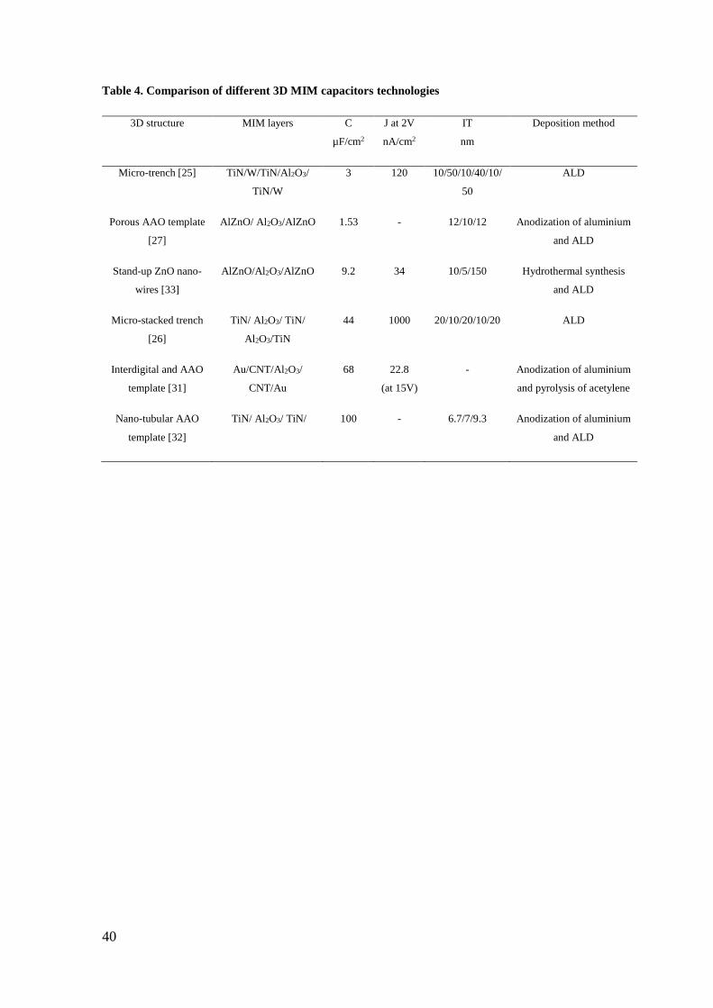
Table 4 summarizes the characteristics of the mentioned 3D-MIM capacitor technologies
with high capacitance density for high energy storage applications. Anodic aluminum
oxide (AAO) templates are mainly used for high energy storage applications because they
can be economically scalable. In addition, they show high dielectric constant, high band
gap and low density of aluminum oxide as was shown in Table 2.
40
Table 4. Comparison of different 3D MIM capacitors technologies
3D structure MIM layers C
µF/cm2
J at 2V
nA/cm2
IT
nm
Deposition method
Micro-trench [25] TiN/W/TiN/Al2O3/
TiN/W
3 120 10/50/10/40/10/
50
ALD
Porous AAO template
[27]
AlZnO/ Al2O3/AlZnO 1.53 - 12/10/12 Anodization of aluminium
and ALD
Stand-up ZnO nano-
wires [33]
AlZnO/Al2O3/AlZnO 9.2 34 10/5/150 Hydrothermal synthesis
and ALD
Micro-stacked trench
[26]
TiN/ Al2O3/ TiN/
Al2O3/TiN
44 1000 20/10/20/10/20 ALD
Interdigital and AAO
template [31]
Au/CNT/Al2O3/
CNT/Au
68 22.8
(at 15V)
- Anodization of aluminium
and pyrolysis of acetylene
Nano-tubular AAO
template [32]
TiN/ Al2O3/ TiN/ 100 - 6.7/7/9.3 Anodization of aluminium
and ALD

41
2.2. Supercapacitors
2.2.1. Supercapacitor concept
Supercapacitors (SCs) are electrochemical devices used as short-term energy store
supplies [34] in many applications as electric vehicles, uninterruptible power systems or
as voltage stabilizer in wind and photovoltaic systems, among others. Figure 16 shows
some system examples where the energy support and the power transfer are required from
SCs.
Figure 16. Examples of systems where SCs are found: trams (Barcelona), hydride cars (Toyota)
and uninterruptible power supplies.
Table 5 shows a comparison of conventional capacitors, supercapacitors and batteries.
SCs have a higher cycle life and power density than the batteries as it can be seen in Table
5. Furthermore, they are fabricated with no-polluting materials that do not produce
hazardous waste such as lead or cadmium. These features position them as a good green
alternative to the batteries.
The fact that the supercapacitors (up to 10kW/Kg) may storage energy to a higher power
density than batteries (up to 1kW/Kg), indicates that SCs are faster transferring energy
than batteries, but the supercapacitors are not as faster as conventional capacitors (over
10kW/Kg). Another leading feature of the supercapacitors is that they can handle more
energy (1Wh/Kg) than the MIMs or other conventional capacitors (up to 0.1Wh/Kg).
However, the energy density is still smaller than batteries (from 10 to 100 Wh/Kg).

42
Table 5. Comparison of capacitors, supercapacitors and batteries (source [35]).
Factor Conventional capacitors Supercapacitors Batteries
Cycle-life Almost infinite >500000 About 1000
Power density (kW/Kg) Greater than 10 Between 0.5 and 10 Less than 1
Energy density (Wh/Kg) Lower than 0.1 Between 1 and 10 Between 10 and 100
Charge/Discharge Efficiency
(%)
Around 100 Between 85 and 98 Between 70 and 85
The charge/discharge efficiency means that virtually all the energy stored in the MIM
capacitors can be delivered, whereas supercapacitors have greater losses due to leakages
and electrolyte degradation obtaining efficiencies from 85% to 98%.
The supercapacitors industry is in continuous growth. The global supercapacitors market
is expected to reach USD 2billons in 2022 according to a study carried out by Zion Market
(Figure 17). The increasing demand of the supercapacitors is associated to the use in smart
grid applications (wind and solar energy), the pressing demand in the automotive industry
(hybrid electric vehicles) and electric transportation systems (trains, subways, buses and
elevators), among other applications.
Figure 17. Supercapacitors marked forecast (source [36]).
The energy density values achieved by SCs are due to the high capacitance density which
is essentially determined by the enhancement of the contact area (high specific surface
area) combined with electrolytes that provide electrochemical charges. The energy in the

43
SCs is mostly electrostatic due to the electrical double layers formed within the electrode-
electrolyte interfaces, while in the batteries the stored energy is purely chemical.
The electrical double layers are formed by electrolyte ions that have diffused toward the
electrode pores and the electrostatic charges of the electrodes. In Figure 18 shows an
example of an SC is constituted by two porous electrodes (anode and cathode) such as
activated carbon, soaked in an electrolyte, for instance sulphuric acid. A separator that is
usually is fiberglass or a paper or a poly-tetrafluoroethylene (PTFE) membrane prevents
electrodes from coming into electrical contact.
Figure 18. Schematic of a supercapacitor including the anode, cathode, electrolyte and the
electrical double layers.
Supercapacitors are classified into three types: Electrical double layer capacitor (EDLC),
pseudocapacitor and hybrid capacitor. EDLC are those whose charge accumulation is
purely electrostatic and there is no transfer of charge across the electrode-electrolyte
interface. The electrodes material of EDLC capacitors is usually based on carbon
materials and derivatives.
Another kind of SC with enhanced specific capacitance is the Pseudocapacitor which is
based on electrochemical reduction-oxidation (redox) mechanisms yielded in the

44
interface with conducting polymers or transition metal oxides (RuO2, TiO2, MnO2) as
electrodes. Finally, the hybrid capacitor based on the combination of both categories.
The operating voltage, capacitance and equivalent series resistance (ESR) are the main
parameters defined for SCs. Table 6 shows typical values for commercial SCs.
Table 6. Some available commercial SCs and characteristics (source: [37]).
Manufacturer Voltage (V) Capacitance (F) ESR (mΩ)
APowerCap 2.70 55 -
APowerCap 2.70 450 -
Asashi Glass 2.70 1375 2.50
BatScap 2.70 2680 0.20
Fuji 3.80 1800 1.50
Ioxus 2.70 3000 0.45
Ioxus 2.70 2000 0.54
JSR Micro 3.80 1100 1.15
JSR Micro 3.80 2300 0.77
LS Mtron 2.80 3200 0.25
Maxwell 2.70 2885 0.38
Maxwell 2.70 605 0.90
NessCap 2.70 1800 0.55
NessCap 2.70 3640 0.30
Panasonic 2.30 0.10 0.08
Panasonic 5.50 50 0.08
PowerStor 2.50 2.20 4.57
PowerStor 16.20 65 7.00
Skeleton 3.40 3200 0.47
Skeleton 3.40 850 0.80
VinaTech 2.70 336 3.50
VinaTech 3.00 342 6.60
Yunasko 2.70 510 0.90
Yunasko 2.75 1275 0.11
Yunasko 2.70 7200 1.40
The operating voltage, also known as window voltage, depends on the stability of the
electrolyte (decomposition voltage of the electrolyte). Three type of electrolytes are used
in SCs: aqueous such as sulfuric acid (H2SO4) or potassium hydroxide (KOH) [38],
organic such as propylene carbonate (PC) or acetonitrile (AN) with tetraethyl-ammonium
tetra-fluoroborate salt (TEABF4) [39], and ionic liquids in recent research [40]. Using
activated carbon electrodes, the cell working voltage ranges from 2.3V to 2.7V for
organic electrolytes, 0.8-1.0V for aqueous electrolytes and 3-4V for ionic liquid
electrolytes [38].
As mentioned before, the main defining parameter of a SC is the capacitance, but there is
a more specific parameter, that is the specific capacitance, that takes into account the
charge storage ability of the supercapacitor active material, defined as:

45
𝐶𝑆 =𝑑𝑄
𝑑𝑉∀ ( 19 )
Where Ɐ may define the mass, the volume, or the surface area of the electrodes or the
active material.
If Ɐ is the mass, CS is termed as gravimetric capacitance (F/g), also denoted as CW.
If Ɐ is the volume, CS is termed as volumetric capacitance (F/cm3), also denoted as CV.
If Ɐ is the electrochemical surface area (real area), CS is termed as area-specific,
normalized, differential, intrinsic, interfacial or double layer capacitance (µF/ cm2), also
denoted as CD.
If Ɐ is the geometric area, CS is termed as areal capacitance (F/cm2).
The specific surface area (SSA) is the total surface area of the microspores electrode
measured using the standard technique known as Brunauer–Emmett–Teller (BET)
method [41] which is based on the phenomenon of adsorption of a gas (Nitrogen at 77K)
into a solid, the units are m2/g [42]. The specific surface area is useful to estimate the
double layer capacitance. For instance, if the CW = 11mF/cm2 and the SSABET =2371m2/g,
then the double layer capacitance is 9.9 µF/ cm2 [43].
2.2.2. Supercapacitors classification.
As mention before, the supercapacitors area may be classified according to the conductive
electrode material. The electrode material is often referred to as the active material.
While the electrolyte, the binder and the current collector are called inactive materials.
Figure 19 shows a classification of the supercapacitors regarding the active material used
in each one.

46
Figure 19. Classification of supercapacitors: The Electrical Double Layer, Pseudo and Hybrid
Capacitors.
Figure 20 summarizes some active materials used in SCs and their specific capacitances
[44]. Carbon based material are widely studied but do not top the list of materials that
provide greater specific capacitance.
Figure 20. Specific capacitance of active materials in supercapacitors (source [44]).

47
Composites of redox-active materials as ruthenium oxide (RuO2) exhibit higher
capacitances than carbon-based and conducting polymer materials. However, despite this
potential, the success of RuO2 has been inadequate by its excessive cost and toxicity. As
it can be seen, there are many technology approaches on the fabrication of SCs. Therefore,
SCs have an extensive range of possibilities that require a very specific study for each
material. This thesis is focused on capacitors which may be half way between MIMs and
EDLCs supercapacitors, for this reason, this section is mainly showing characteristics of
EDLCs and not of pseudo-capacitors or hybrids.
2.2.3. Advances in Electrical Double Layer capacitors
Activated carbon is the material mostly used as active material in the SC industry. It is
usually a powder transformed into a solid electrode with a high specific surface area of
1000-3000m2/g [45] [46] [43], including a binder such as polytetra-fluoroethylene
(PTFE), poly-methylcellulose, polystyrenestyrene/butadiene copolymer or
ethylene/acrylic acid copolymer [47]. The raw material (precursor) of the activated
carbon can be coal, coconut, shells, peat, wood and petroleum based residues, that is,
materials with a high carbon content which are processed by thermal activation (900ºC)
with oxidizing gases (such as CO2, H2O or O2) or chemical activation (such as KOH).
Figure 21 sums up the preparation process of activated carbon.
Electrodes based on activated carbon have specific capacitances between 100-300F/g or
a double layer capacitances of 15-50μF/cm2 depending on the electrolyte [38] [46] or the
activation method [43]. With organic electrolytes, the specific capacitance is about of
100F/g or 70F/cm3 [48].
Figure 21. Diagram of the fabrication process of activated carbon.

48
The density of an activated carbon is in the range of 0.4-0.8g/cm3, the thickness is usually
in the range of 100-300µm, then the capacitance of an electrode of a thickness (t), area
(A) and density (ρ) can be calculated as [38]:
𝐶 = (𝐹/𝑔)𝜌𝑡𝐴 ( 20 )
Activated carbon is composed by structures with size pores [43] in the range of
micropores (<2nm), mesopores (2-50nm), and macropores (>50nm). The pore diameters
are classified by International Union of Pure and Applied Chemistry (IUPACH) [49]. The
structures with micropores are the most used [38] mainly in supercapacitors with aqueous
electrolytes like KOH. They are, however, not so effective for organic electrolyte because
organic ions are bigger than those pores [45].
Experimentally, capacitance does not always have a lineal relation with the surface area
of an active carbon, first, due to that all pores may not be accessible to the electrolyte
ions; and second, because the double layer varies with various types of activated carbons
(different precursors and activation methods).
Figure 22 shows the SEM images of two carbon electrode samples. The first (left)
electrode sample, it is fabricated by a mixture of 92% activated carbon, 5% acetylene
black and 3% PTFE that shows carbon grains with a size up to 10 µm, whereas PTFE and
acetylene black particles (binder) are in the order of 0.1 µm. The second electrode (right)
has grains with sizes ranging around 1µm and 0.1µm, it is a carbon electrode extracted
from a commercial SC cell package. It should be noted that PTFE is the binder used to
hold activated carbon grains together and carbon black is an additive to raise the electrode
conductivity.

49
Figure 22. SEM images of activated carbon electrodes extracted (a) from a specific fabricated
electrodes and (b) a commercial one (source [50]).
Inverse opal carbon templates [51] using silica colloidal crystal as a opal template and
a polymer as carbon precursor have been tested as electrode material for EDLC
capacitors. An inverse opal carbon structure using poly-furfuryl alcohol as a precursor in
an organic electrolyte, showed a specific capacitance up to 100F/g and a specific surface
area from 600 to 1200m2/g. The fabrication process can be seen in Figure 23. The silica
nanoparticles crystal was sintered at 1100ºC. Afterwards, poly-furfuryl alcohol was
poured over the silica opal template. Then, it was carbonated at 1000ºC producing a
carbon/silica composite. Finally, the silica nanoparticles were etched off with a
hydrofluoric acid solution, resulting a cavernous carbon template.
Figure 23. Inverse opal carbon template: (a) Fabrication steps (b) SEM image (source [51]).

50
Carbide derived carbons (CDCs) [52] are carbons derived from metal carbides
compounds such as TiC, SiC, Mo2C, B4C, by selective chlorine (Cl2) etching of metals.
Electrodes based on CDCs provide uniform distribution of pores and high specific area
from 1000 to 2000 m2/g [53]. A specific capacitance ranging from 100F/g to 130F/g [52]
was obtained for CDC SC electrodes using micro-sized titanium carbide (TiC) particles
as precursor in organic electrolytes. Figure 24 shows a SEM image of carbon powder
synthetized from TiC particles. The fabrication of templated CDC have given good
results, as an example, a mesoporous SiC derived carbon (CDC) [54] showed a specific
capacitance up to 170F/g using tetraethylammonium tetrafluoroborate (TEABF4) solution
in acetonitrile, and a specific surface area up to 2430 m2/g.
Figure 24. A SEM image of the surface of carbide derived carbon synthetized from TiC. (source
[52]).
Carbon nanotubes (CNTs) are large molecules consisting of carbon atoms rolled in a
cylinder shape [55] with diameters in the nanometre range and lengths from micrometres
to centimetres. CNTs are nano-materials widely researched as SC active material because
of their high surface area, electrical conductivity, corrosion resistance and temperature
stability. There are two CNT types: single-walled carbon nanotube (SWNT) or multiple-
walled carbon nanotube (MWNT). A SWNT consist of a cylindrical wall of single-layer
carbon atoms (graphene). Whereas a MWNT are several concentric nanotubes inside
other nanotubes with diameter between 3 to 30nm [56].

51
The CNT structures usually achieve better performance than activated-carbon mainly
because their micro and meso-pores distribution give them better electrolyte accessibility
[57] than activated carbon structures to reach high capacitances. Moreover, CNTs are
electrically more conductive (5000Scm-1) [58] than activated carbon (0.5-2Scm-1) [59]
which produces a higher energy transfer than in activated carbon.
The CNTs can be synthetized by different methods such as arc-discharge method, laser-
ablation method, catalytic decomposition of hydrocarbons, pyrolysis of hydrocarbons,
plastic and chemical vapour deposition CVD processes. However, no method is still
viable for large scale commercial production due to the high manufacturing cost [60].
Figure 25 shows the SEM image of a randomly entangled SWNTs electrode [61] in a
KOH electrolyte that achieved a maximum specific capacitance of 180F/g. The nanotubes
were synthetized using the arc-discharge method with a heat treatment temperature at
1000ºC. A binder was used for the adhesion of the nanotubes between them.
Figure 25. SEM images of randomly entangled and cross-linked SWNT (source [61]).
Figure 26 shows a TEM image of commercial catalytically grown MWNTs that were
functionalized with nitric acid to introduce oxygenate groups. The MWNTs cell using a
H2SO4 electrolyte exhibited a specific capacitance of up to 102F/g [62]. A benefit of
functionalization is that it contributes to a good self-adhesion of the MWNTs.

52
Figure 26. TEM image of randomly entangled and cross-liked MWNTs with an average diameter
of 8nm (source:[62]).
The porosity of the CNTs can be improved by chemical KOH activation in order to
enhance the specific surface area (structures with 470m2/g improved their surface to
weight value up to 1470-3802 m2/g after activation) [63], and to obtain enhanced
capacitance density values of MWNT supercapacitors [64] (from 15F/g to 90F/g after
activation). Besides, the capacitance may be enhanced with thermal annealing processes
oxidizing of CNTs till a specific temperature [55], since the capacitance can also decrease
due to the reduction of the surface area. For instance Li et al [65] annealed entangled
MWCNT at different temperatures finding that the specific capacitance increased from
23F/g to 48F/g with at a temperature treatment of 650ºC, but the specific capacitance
dropped for higher heating temperature values. In the literature, a BET specific surface
area has been reported of up to 1600 m2/g for SWNT and around 400 m2/g for MWNT
have been reported [57].
The CNTs can be arranged in aligned or non-aligned forms. Aligned CNTs are more
desirable because they have shown to provide more surface access to the electrolyte. A
vertical aligned CNT electrode [66] showed a capacitance density of 440 F/g using 1-
ethyl-3-methylimidazolium tetrafluoroborate (EMIBF4) as ionic liquid electrolyte.
Aligned carbon nanotubes can be produced by plasma-enhanced chemical vapour
deposition (PECVD) [67] [68] on thin film of iron or nickel, while chemical vapour
deposition (CVD) can produce non-aligned CNTs as it observed in Figure 27. Carbon
arc-discharge, pyrolysis of hydrocarbons and pulsed laser vaporization [58] are different

53
processed to synthetize non-aligned CNTs, that also have applications in other industries
[69] [70].
Figure 27. SEM pictures of different CNT arrangements: (a) curly and non-aligned CNTs using
thermal CVD, (b) vertical aligned CNTs using PECVD (source [67]).
Vertical aligned single-walled carbon nanotubes (SWNT) [71] have also been also grown
with water-assisted chemical vapor deposition synthesis reaching heights of up to 2.5mm
in a 10 minute growth time with a high carbon purity of 99.98%. Figure 28 shows images
of a very dense SWCNT forest synthesized with this mentioned method.
Figure 28. SWNT forest synthesized with water assisted CVD (source [71]).
As an example of a hybrid SC, Polyaniline (PANI), a conducting polymer, added in the
CNTs contributed to an increase in the specific pseudo-capacitance as it has been reported

54
in a structure of a SC based on Vertical Aligned Carbon Nanotubes and PANI
nanocomposite electrodes [72]. The device showed a specific capacitance of 403.3 F/g in
HClO4 electrolyte and 314.6 F/g in EMIBF4 electrolyte; the schematic of the designed
structure of the SC electrode is observed in Figure 29, disordered entangle CNTs are
vertical aligned and PANI is polymerized on the VA-CNTs.
Figure 29. Schematic illustration of the fabrication of the PANI/VA-CNTs electrodes (source [72] ).
On the other hand, graphene is a single graphite atom layer which has a much higher
conductivity (106 Scm-1) than CNTs (5x10³Scm-1) [58] and a very high specific surface
area of 2630 m2/g [58]. Graphene was first synthesized by Geim and Novoselov in 2004
[73] from a commercial pyrolytic graphite sheet [74], previously etched in oxygen
plasma. The graphite was stuck, pressed and detached from a scotch tape, leaving thin
graphite flakes that were put on a silicon wafer. Then, it was discovered that the thin
graphite flakes contented few layer of graphene. Nowadays, there are different synthesize
methods including: mechanical exfoliation of graphite in solutions [75] [76] , thermal
chemical vapor deposition (CVD), plasma enhanced CVD [74] and synthesis of graphene
oxide and the reduction [77]. The control of these processes and the fact that graphene
has a theoretical maximum specific capacitance of 550F/g [78], are opening novel
opportunities to the large scale fabrication of graphene-based SCs.
Figure 30a shows the structure of a flexible SC [79] using two graphene electrodes and
poly vinyl alcohol/phosphoric acid (PVA/H3PO4) gel electrolyte and polyethylene-
terephthalate (PET) as substrate, showing a capacitance of 12.4µF/cm2. The graphene was

55
fabricated by means of a rapid thermal annealing (RTA) process of Ni/carbon/SiO2/Si
substrate and it was then transferred to the PET substrate.
Figure 30. Images of a (a) flexible graphene supercapacitor (source [79]) on PET substrate.
Schematic of another (b) flexible graphene supercapacitor (source [80]) on paper substrate.
L. Fekri et al [80] reported another flexible SC example, consisting of both sides paper
substrates using graphene as electrode material, PVA/H3PO4 as gel electrolyte and
BaTiO3 as gel separator. The resulting specific capacitance ranges in this case from 87F/g
to 410F/g. The schematic of symmetric SC is showed in Figure 30b. In these examples,
PVA/H3PO4 makes up a known solid polymer electrolyte (SPE), where H3PO4 works as
an ionic liquid and PVA as a polymeric matrix. A SPE has the ability to be flexible,
transparent, lightweight and stable with temperature.
Graphene oxide (GO) is an insulator material, but reduced graphene oxide (RG-O)
platelets yielded after a heating treatment of oxide graphene suspensions, gained electrical
conductivity (5230 S/m) due to the removal of oxygen groups. So, Yanwu Zhu et al [81]
reported a specific capacitance of about 120F/g for two SCs fabricated with RG-O
platelets as electrodes with an electrolyte of propylene carbonate (PC) with TEABF4.
Figure 31 shows the SEM image of wrinkled platelets of RG-O obtained by exfoliation
of graphene oxide suspension in PC at 150ºC followed by vacuum drying.

56
Figure 31. SEM image of RG-O platelets obtained by heating graphene oxide in PC (source [81] ).
Without using a binder, porous graphene electrodes were fabricated by the electrospray
of graphene oxide (GO) nanoparticles on stainless steel substrates. Crumpled reduce
graphene oxide (C-RGO) structures were obtained after a hydrazine-thermal reduction
treatment process. The SC cell exhibited a specific capacitance 366F/g [82] using KOH
as aqueous electrolyte. Figure 32 shows a schematic of the fabrication process. This work
made electrospray to attract attention as a method of depositing graphene. A. Varea et al
[83] analyzed the electrospray deposition condition to deposit GO and RGO onto rigid
and flexible substrates from GO and RGO nanoparticles dispersed in isopropanol using
electrospray technique under ambient conditions.
Figure 32. Schematic of the fabrication process of C-RGO from GO solution using electrospray
technique. C-GO is reduced in the hydrazine hydrate vapour at 85 °C, source [82].

57
Recently, J. Yan et al [84] fabricated a graphene SC using the electrospray technique with
a moving stage. The GO solution was electrosprayed at 8kV on polyamide nanofiber
film/aluminium foil, then a post-treatment was performed with a GO film as it can be
seen in Figure 33. Summarizing, the electrosprayed GO film was separated from the foil
in order to obtain a reduced GO by means of the immersion of GO into a hydro-iodic (HI)
acid solution at 100 ºC. The specific capacitance in KOH electrolyte was 174 F/g.
Figure 33. Schematic of the fabrication of a RGO electrode. (source [84]).
Table 7 sums up several mentioned electrode materials used in EDL supercapacitors, it is
included the electrolyte, the specific capacitance, the electrode cost and electrode
conductivity are included. The capacitance of the different active materials varies with
the type of electrolyte used, but carbon nanotubes and graphene electrodes using ion
liquid electrolytes show higher capacitances and higher conductivities, thus both
materials are the best in terms of performance. However, physicochemical modification
of activated carbon continues improving the performance of SC electrodes with capacities
as high as 450F/g [85]. For that reason and added to the fact that they are more economical
than CNT or graphene electrodes, activated carbon is still the active material that
dominates currently full-scale manufacture of SC. In terms of costs, graphene could be
competing a candidate as long as it reduces their costs. Graphene electrodes have
moderate costs at the present time. All of these factors should be considered to improve
the existing technologies.

58
Finally, the gravimetric capacitance is an important parameter in the electrochemical
field, because they characterize the capacitance over the electrode mass more than
capacitance over the area. Therefore, the areal capacitance and double layer capacitance
(defined in the section 2.2.1.) are rarely itemized. In order to present a broader catalog of
parameters, Table 8 sums up these specific capacitances found in the literature.
Table 7. Comparison of different carbon based electrode materials used in EDLCs.
Electrode Electrolyte Cs (F/g)
[86]
Cost
[87]
Conductivity
[87]
Activated carbon
[38] [43] [85]
Aqueous: KOH or H2SO4 100-450 Low Low
Activated carbon
[88] [39]
Organic: (C2H5)4NBF4 with acetonitrile or
acetonitrile with
tetraethylammoniumtetrafluoroborate
(Et4NBF4)
~100 Low Low
Inverse opal carbon
[89] [90]
Aqueous: KOH 130-220 High Low
Inverse opal carbon
[51]
Organic: Tetraethylammonium
tetrafluoroborate (Et4NBF4) in acetonitrile
~100 High Low
Carbide derived
carbon [52]
Organic: Tetraethylammonium
tetrafluoroborate (Et4NBF4) in acetonitrile
(CH3CN)
100-130 Moderate Moderate
Carbide derived
carbon [86] [52]
Ionic liquids: 1-Ethyl-3-methylimidazolium
bistrifluoromethylsulfonylimide (EMIM
TFSI) in acetonitrile (CH3CN)
100-150 Moderate Moderate
Carbon nanotubes
[86]
Aqueous: NaOH or KOH 20 - 180 High High
Carbon nanotubes
[66]
Ionic liquid: 1-ethyl-3-methylimidazolium
tetrafluoroborate EMIBF4
~440 High High
Reduced Graphene
oxide (rGO) [86]
Organic:Tetraethylammonium
tetrafluoroborate (Et4NBF4)
10 - 150 Moderate high
Graphene oxide
[91]
Aqueous: KOH ~190 Moderate high
(Curved) Graphene
[92]
Ionic liquid: EMIMBF4. 100-250 Moderate high
Graphene [80] Ionic liquid: PVA/H3PO4 87 - 410 Moderate high
Table 8. Areal capacitance and double layer capacitance of carbon materials
Electrode material Areal capacitance (mF/cm2) Double layer capacitance (µF/cm2)
Activated carbon 10-50 [46] 5-50 [58] [93] [46]

59
Nanotube 8 [94] - 16 [42] 6-24 [35]
Graphene ~ 40 (rGO-gel) [78] in KOH ~21 [74] [95] in a ionic liquid (BMIM- PF6).
2-9 [93] in KOH

60
2.3. References
[1] J.-. Arnould, P. Benech, S. Cremer, J. Torres, and A. Farcy, “RF MIM capacitors
using Si/sub 3/N/sub 4/ dielectric in standard industrial BiCMOS technology,” in
2004 IEEE International Symposium on Industrial Electronics, 2004, vol. 1, pp.
27–30 vol. 1.
[2] “CUSTOM SYSTEM-ON-CHIP (SOC),” Arm Limited, 2019. [Online]. Available:
https://www.arm.com/why-arm/custom-socs. [Accessed: 15-Sep-2019].
[3] S. Van Huylenbroeck, S. Decoutere, R. Venegas, S. Jenei, and G. Winderickx,
“Investigation of PECVD dielectrics for nondispersive metal-insulator-metal
capacitors,” IEEE Electron Device Lett., vol. 23, no. 4, pp. 191–193, 2002.
[4] B. J. Hutchinson, “An Investigation of High- k Materials in Metal-Insulator-Metal
Capacitor Structures,” NATIONAL UNIVERSITY OF IRELAND, CORK, 2017.
[5] “The International Technology Roadmap for Semiconductors (ITRS). Table
RFAMS4 On-Chip Passives Technology Requirements,” 2012. [Online].
Available: http://www.itrs2.net/2012-itrs.html. [Accessed: 18-Oct-2019].
[6] M. A. Zulkifeli, S. N. Sabki, S. Taking, N. A. Azmi, and S. S. Jamuar, “The effect
of different dielectric materials in designing high performance Metal-Insulator-
Metal (MIM) capacitors,” Int. J. Electr. Comput. Eng., vol. 7, no. 3, pp. 1554–
1561, 2017.
[7] S. B. Chen, C. H. Lai, A. Chin, J. C. Hsieh, J. Liu, and A. L. F. Characteristics,
“High-Density MIM Capacitors Using High-K Al2O3 and AlTiOx Dielectrics,”
Electronics, vol. 23, no. 4, pp. 201–204, 2002.
[8] M. M. Krasnov, S. E. Avetisov, N. V. Makashova, and V. R. Mamikonian, “A
High Performance MIM Capacitor Using HfO2 Dielectrics,” IEEE ELECTRON
DEVICE Lett., vol. 23, no. 6, pp. 27–30, 2002.
[9] M. Y. Yang, D. S. Yu, and A. Chin, “High-Density RF MIM Capacitors Using

61
High-k La2O3 Dielectrics,” J. Electrochem. Soc., vol. 151, no. 7, p. F162, 2004.
[10] B. Hudec et al., “Electrical properties of TiO2-based MIM capacitors deposited by
TiCl4 and TTIP based atomic layer deposition processes,” Microelectron. Eng.,
vol. 88, no. 7, pp. 1514–1516, 2011.
[11] D. Kannadassan, R. Karthik, M. Shojaei Baghini, and P. S. Mallick,
“Nanostructured metal-insulator-metal capacitor with anodic titania,” Mater. Sci.
Semicond. Process., vol. 16, no. 2, pp. 274–281, 2013.
[12] J. Robertson, “High dielectric constant oxides,” Eur. Physcial J. Appl. Phys., vol.
28, pp. 265–201, 2004.
[13] S. A. Sherrill, P. Banerjee, G. W. Rubloff, and S. B. Lee, “High to ultra-high power
electrical energy storage,” Phys. Chem. Chem. Phys., vol. 13, no. 46, pp. 20714–
20723, 2011.
[14] S. U. Park et al., “Analysis of reliability characteristics of high capacitance density
MIM capacitors with SiO2-HfO2-SiO2 dielectrics,” Microelectron. Eng., vol. 88,
no. 12, pp. 3389–3392, 2011.
[15] C.-S. Ho, S.-J. Chang, S.-C. Chen, J. J. Liou, and H. Li, “A Reliable Si3N4/Al2O3-
HfO2 Stack MIM Capacitor for High-Voltage Analog Applications,” Electron
Devices, IEEE Trans., vol. 61, no. 8, pp. 2944–2949, 2014.
[16] K. Lee et al., “Leakage current suppression in spatially controlled Si-doped ZrO2
for capacitors using atomic layer deposition,” Thin Solid Films, vol. 657, no.
October 2017, pp. 1–7, 2018.
[17] D. Z. Austin, D. Allman, D. Price, S. Hose, and J. F. Conley, “Plasma Enhanced
Atomic Layer Deposition of Al2O3 /SiO2 MIM Capacitors,” Ieee Electron Device
Lett., vol. 36, no. 5, pp. 496–498, 2015.
[18] B. Zhu, X. Wu, W. J. Liu, S. J. Ding, D. W. Zhang, and Z. Fan, “Dielectric
Enhancement of Atomic Layer-Deposited Al2O3 /ZrO2 /Al2O3 MIM Capacitors
by Microwave Annealing,” Nanoscale Res. Lett., vol. 14, pp. 2–7, 2019.
[19] S. J. Kim et al., “Improvement of Voltage Linearity in High- MIM Capacitors
Using HfO 2 – SiO 2 Stacked Dielectric,” Ieee Electron Device Lett., vol. 25, no.

62
8, pp. 538–540, 2004.
[20] J. Yang et al., “Effective Modulation of Quadratic Voltage Coefficient of
Capacitance in MIM Capacitors Using Sm2O3/SiO2 Dielectric Stack,” IEEE
Electron Device Lett., vol. 30, no. 5, pp. 460–462, 2009.
[21] T. H. Phung et al., “High Performance Metal-Insulator-Metal Capacitors with Er
2 O 3 on ALD SiO 2 for RF Applications,” J. ofThe Electrochem. Soc., vol. 158,
no. 12, pp. 1289–1292, 2011.
[22] J. H. Lee, Y. C. Lin, B. H. Chen, and C. Y. Tsai, “New metal-insulator-metal
capacitor based on SrTiO3/Al2O3/SrTiO3laminate dielectric,” in 2010 10th IEEE
International Conference on Solid-State and Integrated Circuit Technology, 2010,
pp. 1024–1026.
[23] C. Lin, Y. Wu, R. Jiang, and M. Yu, “MIM Capacitors Based
onZrTiOxBaZryTi1−yO3Featuring Record-Low VCC and Excellent Reliability,”
IEEE Electron Device Lett., vol. 34, no. 11, pp. 1418–1420, 2013.
[24] S. Park et al., “Analysis of reliability characteristics of high capacitance density
MIM capacitors with SiO 2 – HfO 2 – SiO 2 dielectrics,” Microelectron. Eng., vol.
88, pp. 3389–3392, 2011.
[25] J. Mu, X. Chou, Z. Ma, J. He, and J. Xiong, “High-performance MIM capacitors
for a secondary power supply application,” Micromachines, vol. 9, no. 2, pp. 1–
10, 2018.
[26] J. H. Klootwijk et al., “Ultrahigh capacitance density for multiple ALD-Grown
MIM capacitor stacks in 3-D silicon,” IEEE Electron Device Lett., vol. 29, no. 7,
pp. 740–742, 2008.
[27] L. Li et al., “Three-dimensional AlZnO / Al2O3 / AlZnO nanocapacitor arrays on
Si substrate for energy storage,” Nanoscale Res. Lett., vol. 7, no. 1, p. 1, 2012.
[28] G. Zhang et al., “Transparent nanotubular capacitors based on transplanted anodic
aluminum oxide templates,” ACS Appl. Mater. Interfaces, vol. 7, no. 9, pp. 5522–
5527, 2015.
[29] Y. K. Hong, B. H. Kim, D. Il Kim, D. H. Park, and J. Joo, “High-yield and

63
environment-minded fabrication of nanoporous anodic aluminum oxide
templates,” RSC Adv., vol. 5, no. 34, pp. 26872–26877, 2015.
[30] L. Wei et al., “Low-Cost and High-Productivity Three- Dimensional
Nanocapacitors Based on Stand-Up ZnO Nanowires for Energy Storage,”
Nanoscale Res. Lett., vol. 11, 2016.
[31] F. Han et al., “Dielectric capacitors with three-dimensional nanoscale interdigital
electrodes for energy storage,” Sci. Adv., vol. 1, no. 9, pp. 1–7, 2015.
[32] P. Banerjee, I. Perez, L. Henn-Lecordier, S. B. Lee, and G. W. Rubloff,
“Nanotubular metal-insulator-metal capacitor arrays for energy storage,” Nat.
Nanotechnol., vol. 4, no. 5, pp. 292–296, 2009.
[33] L. Wei et al., “Low-Cost and High-Productivity Three-Dimensional
Nanocapacitors Based on Stand-Up ZnO Nanowires for Energy Storage,”
Nanoscale Res. Lett., vol. 11, no. 1, p. 213, 2016.
[34] M. Al, H. Gualous, N. Omar, and J. Van, “Batteries and Supercapacitors for
Electric Vehicles,” in New Generation of Electric Vehicles, InTech, 2012.
[35] A. González, E. Goikolea, J. A. Barrena, and R. Mysyk, “Review on
supercapacitors: Technologies and materials,” Renew. Sustain. Energy Rev., vol.
58, pp. 1189–1206, 2016.
[36] “Supercapacitor Market,” Zion Market Research, 2019. [Online]. Available:
https://www.zionmarketresearch.com/market-analysis/super-capacitor-market.
[Accessed: 07-Jun-2019].
[37] M. Yassine and D. Fabris, “Performance of commercially available
supercapacitors,” Energies, vol. 10, no. 9, 2017.
[38] A. Burke, “R&D considerations for the performance and application of
electrochemical capacitors,” Electrochim. Acta, vol. 53, no. 3 SPEC. ISS., pp.
1083–1091, 2007.
[39] P. L. Taberna, P. Simon, and J. F. Fauvarque, “Electrochemical Characteristics and
Impedance Spectroscopy Studies of Carbon-Carbon Supercapacitors,” J.
Electrochem. Soc., vol. 150, no. 3, p. A292, 2003.

64
[40] J. Palma, M. Anderson, G. A. Tiruye, D. Mu, and R. Marcilla, “Performance of
solid state supercapacitors based on polymer electrolytes containing different ionic
liquids,” J. Power, vol. 326, pp. 560–568, 2016.
[41] K. S. W. Sing, “Adsorption methods for the characterization of porous materials,”
Adv. Colloid Interface Sci., pp. 3–11, 1998.
[42] J. E. S. J. Signorelli, Riccardo; C-Ku, Daniel; G.Kassakain, “Electrochemical
Double-Layer Capacitors Using Carbon Nanotube Electrode Structures,” Proc.
IEEE, vol. 97, no. 11, pp. 1837–1847, 2009.
[43] K. Kierzek, E. Frackowiak, G. Lota, G. Gryglewicz, and J. Machnikowski,
“Electrochemical capacitors based on highly porous carbons prepared by KOH
activation,” Electrochim. Acta, vol. 49, no. 4, pp. 515–523, 2004.
[44] N. P. Katsuhiko and Simon, “New Materials and New Configurations for
Advanced Electrochemical Capacitors,” J. Electrochem. Soc., vol. 17, no. 1, pp.
34–37, 2008.
[45] S. Sinha, “Studies of activated carbons used in double-layer capacitors,” J. Power
Sources, vol. 74, no. 1–2, pp. 99–107, 1998.
[46] E. Frackowiak and F. Béguin, “Carbon materials for the electrochemical storage
of energy in capacitors,” Carbon N. Y., vol. 39, no. 6, pp. 937–950, 2001.
[47] M. V. KIAMAHALLEH, S. H. S. ZEIN, G. NAJAFPOUR, S. A. SATA, and S.
BUNIRAN, “Multiwalled Carbon Nanotubes Based Nanocomposites for
Supercapacitors: a Review of Electrode Materials,” Nano, vol. 07, no. 02, p.
1230002, 2012.
[48] N. Zhang, S; Pan, “Supercapacitors Performance Evaluation,” Adv. Energy Mater.,
2015.
[49] I. Union, O. F. Pure, and A. Chemistry, “REPORTING PHYSISORPTION DATA
FOR GAS / SOLID SYSTEMS with Special Reference to the Determination of
Surface Area and Porosity,” Pure Appl. Chem., vol. 57, no. 4, pp. 603–619, 1985.
[50] V. V. N. N. Obreja, A. Dinescu, and A. C. Obreja, “Activated carbon based
electrodes in commercial supercapacitors and their performance,” Int. Rev. Electr.

65
Eng., vol. 5, no. February, pp. 272–281, 2010.
[51] S. Tabata, Y. Isshiki, and M. Watanabe, “Inverse opal carbons derived from a
polymer precursor as electrode materials for electric double-layer capacitors,” J.
Electrochem. Soc., vol. 155, no. 3, pp. 42–49, 2008.
[52] B. Dyatkin, O. Gogotsi, B. Malinovskiy, Y. Zozulya, P. Simon, and Y. Gogotsi,
“High capacitance of coarse-grained carbide derived carbon electrodes,” J. Power
Sources, vol. 306, pp. 32–41, 2016.
[53] T. Ariyanto, B. Dyatkin, G.-R. Zhang, A. Kern, Y. Gogotsi, and B. J. M. Etzold,
“Synthesis of carbon core–shell pore structures and their performance as
supercapacitors,” Microporous Mesoporous Mater., vol. 218, pp. 130–136, 2015.
[54] Y. Korenblit et al., “High-rate electrochemical capacitors based on ordered
mesoporous silicon carbide-derived carbon,” ACS Nano, vol. 4, no. 3, pp. 1337–
1344, 2010.
[55] H. Pan, J. Li, and Y. Ping, “Carbon Nanotubes for Supercapacitor,” Nano Rev.,
vol. 5, pp. 654–668, 2010.
[56] K. Z. Kukovecz Á., Kozma G., “Multi-Walled Carbon Nanotubes,” in Springer
Handbook of Nanomaterials, Vajtai R, Ed. Springer, Berlin, Heidelberg, 2013, pp.
147–188.
[57] T. Chen and L. Dai, “Carbon nanomaterials for high-performance
supercapacitors,” Mater. Today, vol. 16, no. 7–8, pp. 272–280, 2013.
[58] L. Dai, L. Dai, D. W. Chang, J. Baek, and W. Lu, “Carbon Nanomaterials for
Advanced Energy Conversion and Storage,” Nano micro small, vol. 8, no. 8, pp.
1130–1166, 2012.
[59] A. Barroso-Bogeat, M. Alexandre-Franco, C. Fernández-González, A. Macías-
García, and V. Gómez-Serrano, “Electrical conductivity of activated carbon-metal
oxide nanocomposites under compression: A comparison study,” Phys. Chem.
Chem. Phys., vol. 16, no. 45, pp. 25161–25175, 2014.
[60] J. Sengupta, “Carbon Nanotube Fabrication at Industrial Scale: Opportunities and
Challenges,” in Handbook of Nanomaterials for Industrial Applications, Elsevier

66
Inc., 2018, pp. 172–194.
[61] B. Kay et al., “Electrochemical Properties of High-Power Supercapacitors Using
Single-Walled Carbon Nanotube Electrodes **,” Adv. Funct. Mater., vol. 11, no.
5, pp. 387–392, 2001.
[62] C. Niu, E. K. Sichel, R. Hoch, D. Moy, and H. Tennent, “High power
electrochemical capacitors based on carbon nanotube electrodes electrodes,” Appl.
Phys. Lett., vol. 70, no. 1489, 1997.
[63] B. Adeniran and R. Mokaya, “Low temperature synthesized carbon nanotube
superstructures with superior CO 2 and hydrogen storage capacity †,” Mater.
Chem. A, vol. 3, pp. 5148–5161, 2015.
[64] E. Frackowiak, S. Delpeux, K. Jurewicz, and K. Szostak, “Enhanced capacitance
of carbon nanotubes through chemical activation,” Chem. Phys. Lett., vol. 361, no.
July, pp. 35–41, 2002.
[65] C. Li et al., “Oxidation of multiwalled carbon nanotubes by air : benefits for
electric double layer capacitors,” Powder Technol., vol. 142, pp. 175–179, 2004.
[66] H. Zhang, G. Cao, Y. Yang, and Z. Gu, “Comparison between electrochemical
properties of aligned carbon nanotube array and entangled carbon nanotube
electrodes,” J. Electrochem. Soc., vol. 155, no. 2, pp. 19–23, 2008.
[67] M. S. Bell, K. B. K. Teo, R. G. Lacerda, W. I. Milne, D. B. Hash, and M.
Meyyappan, “Carbon nanotubes by plasma-enhanced chemical vapor deposition,”
Pure Appl. Chem., vol. 78, no. 6, pp. 1117–1125, 2006.
[68] W. K. Wong, C. S. Lee, and S. T. Lee, “Uniform-diameter, aligned carbon
nanotubes from microwave plasma-enhanced chemical-vapor deposition,” J. Appl.
Phys., vol. 97, no. 8, 2005.
[69] S. Ahmed, A. Aitani, F. Rahman, A. Al-Dawood, and F. Al-Muhaish,
“Decomposition of hydrocarbons to hydrogen and carbon,” Appl. Catal. A Gen.,
vol. 359, no. 1–2, pp. 1–24, 2009.
[70] C. Wu, M. A. Nahil, N. Miskolczi, J. Huang, and P. T. Williams, “Production and
application of carbon nanotubes, as a co-product of hydrogen from the pyrolysis-

67
catalytic reforming of waste plastic,” Process Saf. Environ. Prot., vol. 103, pp.
107–114, 2016.
[71] K. Hata, D. N. Futaba, K. Mizuno, and T. Namai, “Water-Assisted Highly Efficient
Synthesis of Impurity-Free Single-Walled Carbon Nanotubes,” Science (80-. ).,
vol. 306, no. November, pp. 1362–1364, 2004.
[72] G. Wu et al., “High-performance Supercapacitors Based on Electrochemical-
induced Vertical-aligned Carbon Nanotubes and Polyaniline Nanocomposite
Electrodes,” Sci. Rep., vol. 7, no. December 2016, pp. 1–8, 2017.
[73] H. C. Lee et al., “Synthesis of Single-layer Graphene: A Review of Recent
Development,” Procedia Chem., vol. 19, pp. 916–921, 2016.
[74] V. Singh, D. Joung, L. Zhai, S. Das, S. I. Khondaker, and S. Seal, “Graphene based
materials: Past, present and future,” Prog. Mater. Sci., vol. 56, no. 8, pp. 1178–
1271, 2011.
[75] K. Parvez et al., “Exfoliation of Graphite into Graphene in Aqueous Solutions of
Inorganic Salts,” J. Am. Chem. Soc., vol. 136, no. 16, pp. 6083–6091, Apr. 2014.
[76] T. C. Achee et al., “High-yield scalable graphene nanosheet production from
compressed graphite using electrochemical exfoliation,” Sci. Rep., vol. 8, no. 1,
pp. 1–8, 2018.
[77] X. Wang, L. Zhi, and K. Mu, “[Nano Lett.,2008,8,323]Transparent, Conductive
Graphene Electrodes for Dye-Sensitized Solar Cells.pdf,” 2008.
[78] J. Chen, C. Li, and G. Shi, “Graphene materials for electrochemical capacitors,” J.
Phys. Chem. Lett., vol. 4, no. 8, pp. 1244–1253, 2013.
[79] Y. Gao et al., “Transparent, flexible, and solid-state supercapacitors based on
graphene electrodes,” APL Mater., vol. 1, no. 1, p. 7, 2013.
[80] L. F. Aval, M. Ghoranneviss, and G. B. Pour, “High-performance supercapacitors
based on the carbon nanotubes , graphene and graphite nanoparticles electrodes,”
Heliyon, no. September, p. e00862, 2018.
[81] Y. Zhu et al., “Exfoliation of Graphite Oxide in Propylene Carbonate and Thermal

68
Oxide Platelets,” ACS Nano, vol. 4, no. 2, pp. 1227–33, 2010.
[82] H. Tang, C. Yang, Z. Lin, Q. Yang, F. Kang, and C. P. Wong, “Electrospray-
deposition of graphene electrodes: A simple technique to build high-performance
supercapacitors,” Nanoscale, vol. 7, no. 20, pp. 9133–9139, 2015.
[83] A. Varea, O. Monereo, E. Xuriguera, J. Daniel Prades, and A. Cirera, “Electrospray
as a suitable technique for manufacturing carbon-based devices,” J. Phys. D. Appl.
Phys., vol. 50, no. 31, 2017.
[84] J.-X. Yan et al., “Highly Conductive Graphene Paper with Vertically Aligned
Reduced Graphene Oxide Sheets Fabricated by Improved Electrospray Deposition
Technique,” ACS Appl. Mater. Interfaces, vol. 11, no. 11, pp. 10810–10817, Mar.
2019.
[85] H. R. Yu, S. Cho, M. J. Jung, and Y. S. Lee, “Electrochemical and structural
characteristics of activated carbon-based electrodes modified via phosphoric acid,”
Microporous Mesoporous Mater., vol. 172, pp. 131–135, 2013.
[86] A. Muzaffar, M. B. Ahamed, K. Deshmukh, and J. Thirumalai, “A review on recent
advances in hybrid supercapacitors: Design, fabrication and applications,” Renew.
Sustain. Energy Rev., vol. 101, no. October 2018, pp. 123–145, 2019.
[87] C. Rabelais, “TUTORIALS P ROGRAMME ISEE15Cap,” in 4to International
Symposium on Enhanced Electrochemical Capacitors., 2015, no. June.
[88] J. A. Fernández, T. Morishita, M. Toyoda, M. Inagaki, F. Stoeckli, and T. A.
Centeno, “Performance of mesoporous carbons derived from poly(vinyl alcohol)
in electrochemical capacitors,” J. Power Sources, vol. 175, no. 1, pp. 675–679,
2008.
[89] K. Xia, Q. Gao, J. Jiang, and J. Hu, “Hierarchical porous carbons with controlled
micropores and mesopores for supercapacitor electrode materials,” Carbon N. Y.,
vol. 46, no. 13, pp. 1718–1726, 2008.
[90] Y. Zhao et al., “Easy synthesis of ordered meso/macroporous carbon monolith for
use as electrode in electrochemical capacitors,” Mater. Lett., vol. 62, no. 3, pp.
548–551, 2008.

69
[91] Y. Zhu, S. Murali, M. D. Stoller, A. Velamakanni, R. D. Piner, and R. S. Ruoff,
“Microwave assisted exfoliation and reduction of graphite oxide for
ultracapacitors,” Carbon N. Y., vol. 48, no. 7, pp. 2118–2122, 2010.
[92] C. Liu, Z. Yu, D. Neff, A. Zhamu, and B. Z. Jang, “Graphene-based supercapacitor
with an ultrahigh energy density,” Nano Lett., vol. 10, no. 12, pp. 4863–4868,
2010.
[93] H. Ji et al., “Capacitance of carbon-based electrical double-layer capacitors,” Nat.
Commun., vol. 5, no. Cmcm, pp. 1–7, 2014.
[94] X. Chen et al., “Novel electric double-layer capacitor with a coaxial fiber
structure,” Adv. Mater., vol. 25, no. 44, pp. 6436–6441, 2013.
[95] J. Xia, F. Chen, J. Li, and N. Tao, “Measurement of the quantum capacitance of
graphene,” Nat. Nanotechnol., vol. 4, no. 8, pp. 505–509, 2009.

70
CHAPTER III
Compendium of papers
3.1. Paper #1: Impedance modelling of silica nanoparticle metal
insulator metal capacitors.
This work is published in Electrochimica Acta, Volume 280, 2018, Pages 62-70,
https://doi.org/10.1016/j.electacta.2018.05.084.

71

72

73

74

75

76

77

78

79

80
3.2. Paper #2: Capacitive study of a polystyrene nanoparticles
capacitor using impedance spectroscopy.
This work is published in Nanotechnology. 30 (2019) 405702, doi:10.1088/1361-
6528/ab2d58

81

82

83

84

85

86

87
88

89
3.3. Paper #3: Large area deposition of ordered nanoparticle
layers by electrospray.
This is published in Colloid and Interface Science Communications, Volume 25, 2018,
Pages 16-21, https://doi.org/10.1016/j.colcom.2018.06.001.

90

91

92

93

94

95

96
CHAPTER IV
Discussion
4.1. Electrospray deposition conditions of NP-MIMs.
Electrospray deposition method is a low cost, rapid and simple technique that can work
at room temperature. Electrospray allows the targeting of the nanoparticles through a
needle tip into the defined area (the MIM area) by means of a bias voltage between the
needle and the substrate. An image of the electrospray set-up implemented in the
electronic engineering department of the UPC North Campus is in appendix A. The
parameters (Appendix A) for electrospray deposition include the colloidal suspension
material, the applied voltage between terminals, the needle-substrate distances, the
deposition time and the flow rate.
Modifying the electrospray deposition conditions, ordered and disordered nanostructures
can be fabricated. Although, with particles larger than 255nm and under certain voltage
conditions, it is likely to create ordered close-packed nanoparticles, many of the devices
are composed by disordered arrays of nanoparticles. With regard to the deposition
thickness, we experimentally have obtained structures from 1 to 30µm. There is a direct
dependency on the flow rate and deposition time as the nanoparticles layer thickness
increase.
When the deposition contains a high value of water contents the effect known as coffee
stain (or coffee ring) may appear. This effect consists of the accumulation of nanoparticles
that are transported to the edges by means of the evaporation gradient during the drying
phase. The main problem with coffee stain is that on many occasions the top metal is
cracked by nanoparticles deposited bellow.
To improve manufacturing repeatability, the original nanoparticles suspension
(nanoparticles + deionized water) is mixed with isopropanol to decrease surface tension,
reducing the water contents and thus having a shorter jet and Taylor cone. The result is

97
a structure of nanoparticles much more scattered and the elimination of coffee stains. Also
linked to the modification of the suspension, the nanostructure surface roughness
increases, in this case due to the fact that there is no water that left the nanoparticles at
the same level as they dried.
The use of isopropanol also helps to avoid or diminish cracks in the deposition area.
Keeping the NP MIM samples stored in a refrigerator while not in usage, also helps to
diminish the possible cracks of the structures.
4.2. High capacitance of NP-MIM capacitors
Table 9 summarizes the areal capacitance, the capacitance gain, the electrode area,
dielectric layer thickness, the specific capacitance and the deposited nanoparticles mass
of the NP-MIM capacitors presented in the first two papers. The areal capacitance is the
capacitance (C’ derived from equation 6) divided by the area. The so noted capacitance
gain refers to the rate between the measured capacitance respect to theoretical capacitance
of a MIM with a continuous insulator layer of the same dimensions (in the papers it is
denoted as C’/Cth). All devices have the active area of 20.25mm2, except for the sample
silica NP-MIM D that has 3.24mm2. The measurements of the thicknesses are performed
with a SEM/FIB microscopy installed at the UPC multiscale facility. Gravimetric
capacitance is not presented in the papers, but it can be estimated by dividing the
measured capacitance by the mass of the nanoparticles. The mass of the nanoparticles is
estimated from the deposited nanoparticles volume and the density of the solid
nanoparticle.
Silica and polystyrene NP-MIM capacitors showed a capacitance higher than the
expected for the theoretical capacitance of an equivalent conventional MIM capacitor.
For silica NP-MIMs, the specific capacitances (first paper) are 0.18, 0.28 and 2.63 µF/cm2
(MIM A, MIM B and MIM C), that is 589, 449 and 1148 times larger than the theoretical
capacitance. In contrast, the polystyrene NP-MIM capacitor exhibits a specific
capacitance of 15.2nF/cm2, and as we expected is higher than the theoretical film
capacitance, but with a gain factor of 11.7.

98
Table 9. Summary of areal capacitance, gravimetric capacitance and capacitance gain of the reported
NP-MIMs.
MIM
capacitor
Areal
Capacitance
Capacitance
Gain [C’/Cth]
Area
(mm2)
Thickness
(µm)
Gravimetric
capacitance
Mass
(µg)
Paper
Silica NP
MIM-A
0.18 µF/cm2 589 20.25 11.3 0.28 mF/g 124.7 #1
Silica NP-
MIM-B
0.28 µF/cm2 449 20.25 5.49 0.94 mF/g 60.57 #1
Silica NP
MIM-C
2.63 µF/cm2 1148 20.25 1.51 31.9 mF/g 16.67 #1
Silica NP
MIM-D
0.91 µF/cm2 268 3.24 1.01 16.5 mF/g 1.788 #1
Polystyrene
NP MIM
15.3 nF/cm2 11.7 20.25 1.75 0.28 mF/g 11.00 #2
The areal capacitances are in the order of the state of the art of integrated planar MIM
capacitors (~µF/cm2). This is amazing because the integrated MIMs have been
developing for many years using high-k dielectric with thicknesses much smaller than the
NP-MIM capacitors shown in this work, with a technology that is obviously not yet
mature. Capacitance gains as high as 1000, makes them a good start point to use them as
supercapacitors (SC). Nevertheless, the best areal capacitance value is 5703 times lower
than activated carbon based electrodes which average value is about of 30mF/cm2 (see
Table 8 in the section 2.2). A SC assembled with two symmetry activated carbon based
electrodes of 100F/g has 784 times more specific capacitance than the silica NP-MIM C.
Of course it is too ambitious to believe that these early NP MIMs can compete with the
current SCs. Although MIMs and SCs are electrostatic capacitors, only SCs use porous
electrodes and an electrolyte. The NP-MIM capacitors use at the moment is deionized
water as electrolyte, which is in fact a bad electrochemical conductor. In most fabricated
NP-MIM, the maximum operating voltage is around 1.5V, higher than aqueous
supercapacitors, which maximum voltage is about of 1V.
Regarding to the capacitance behaviour, we found out that the capacitance decreases
when the frequency increases. To complement the mentioned, the capacitance dispersion
log-log plot of our reported (paper #1 and paper #2) NP-MIM capacitors are shown in
Figure 34. The largest capacitance is found for the thinnest NP-MIM. The thickness of
the insulating nanoparticles layer is in brackets.

99
We propose that the high capacitance gain can be attributed to the interface polarization
and to the humidity at the nanoparticles interstices and electrode interfaces. Therefore,
electrons, hydrogens (H+), hydroxyls (OH-) and hydroniums (H3O+) moving around the
periphery of the nanoparticles are the charge carries. Comparing the results of the
fabricated NP-MIM samples, polystyrene NP-MIM capacitors have usually a lower
capacitance or capacitance gain than silica NP-MIM. The explanation is most likely due
to hydrophobic surface of the PS nanoparticles that contributes poorly to retain and
transfer charges on the nanoparticles surface, whereas silica nanoparticles have the ability
of attract charges from the environment.
As mentioned before, we suppose that the high capacitance gain can be attributed to the
charge carries at the interstices brought by water molecules. In order to support our
assumption, we proceeded to heat two specific built NP-MIM capacitors (silica NP-MIM
D and polystyrene NP-MIM) till 50ºC. The effect of temperature increase is the
decreasing in capacitance as it can be seen in Figure 35 and Figure 36. From our point of
view, when the temperature increases, the interfacial adsorbed water concentration
decreases, and thus the charge carries decrease. The reduction of the performance for both
silica and polystyrene NP-MIMs also be observed in Figure 6 and Figure 7 embedded in
the text of the paper #1 and paper #2 respectively.
Figure 34. Capacitance behaviour of the NP MIM capacitors versus frequency at room
temperature.

100
Figure 35. Capacitance versus frequency at different temperature for silica NP MIM D.
Figure 36. Capacitance versus frequency at different temperature for polystyrene NP MIM.
Furthermore, in order to know if the humidity effectively affects the NP-MIM behaviour
(results not published yet), two more devices were fabricated (silica NP-MIM E and

101
polystyrene NP-MIM 2). The MIM area for both samples is 15.9mm2, and the thicknesses
are 3.11 µm and 5.4µm respectively. The capacitance of the NP-MIM capacitors under
controlled conditions is measured using a climatic chamber (UPC south campus H9
electronic lab) at different relativity humidity values and at a constant temperature of
25ºC. As predicted the capacitance decreases when decreasing the relativity humidity as
it is clearly shown in Figure 37 and Figure 38 (Appendix B), the maximum capacitance
gains are 1760 and 9.41 at 90% RH for silica NP-MIM E and polystyrene NP-MIM 2
respectively. This corroborates the idea that the charges partially responsible for the
capacitance enhancement are brought by water molecules at the nanoparticles surfaces.
In addition, in the case of silica nanostructures, the humidity also helps to increase the
operating frequency range of the capacitive behaviour. As can be seen in Figure 43 for
silica NP-MIM-E at 90% RH, the normalized reactive power is higher than the
normalized active power up to the crossing point at 1.2kHz where both normalized
powers match, that is, in all this frequency range the silica nanostructure behaves as a
capacitor (Q/|S| > P/|S|), while above 1.2khz it has a resistive behaviour (P/|S| > Q/|S|).
However, decreasing the humidity value up to 40% decreases the crossing point at
1.05Hz. In contrast, capacitive behaviour for the polystyrene NP -MIM-2 capacitor does
not vary with humidity over the entire frequency range, as it can be seen in Figure 44.
4.3. NP-MIMs modelling.
The NP-MIM have been characterized by impedance spectroscopy measurements. The
model used to the theoretical validation of the measurements is a modified Randle circuit
formed by sub-circuits of distributed elements that are shown in Figure 5D (paper #1) for
silica nanoparticles. The nanoparticles-metal interfaces are represented by sub-circuits of
a CPE in parallel to a resistor, while the intermediate nanoparticles are modelled by a
similar sub-circuit, but including a Warburg element in series with the resistor.
Each sub-circuits states for the physics of different parts of the NP-MIM: Since the
nanoparticles have a higher contacting surface with the top metal than with the bottom
metal, the top-interface resistance must be lower than the bottom-interface resistance.
Therefore, the resistance of the top-metal/nanoparticles interface is R3, whereas R2 is the
bottom-metal/nanoparticles interface (R3 < R2 as it can be observed in Table 2 in paper
#1). On the other hand, the sub-circuit containing the Warburg element must be associated
to the diffusion through the nanoparticles. Moreover, we believe that there is a greater

102
concentration of electric charges in the intermediate nanoparticles than in those located
at the interfaces. Hence, this is reflected for the highest capacitance coefficient (QCPE1) of
the central sub-circuit.
Different sub-circuits of the equivalent circuit can be recognized in the Nyquist plot. The
depressed semicircle represents the metal-nanoparticle interface sub-circuits, while the
inclined line is mainly associated to the intermediate nanoparticles sub-circuit. Figure 5
(paper #1) shows that the Nyquist plot for the silica NP-MIM C is more vertical than other
silica NP-MIMs. The fitting revealed that it is because the magnitude of the Warburg
impedance (Aw) is higher than the resistors (R1, R2, R3) and due to the higher values of
QCPE1 compared to QCPE2, QCPE3.
In addition to the impedance spectroscopy characterization, we analyze the transient
response of the NP-MIM capacitors. A silica NP-MIM capacitor is connected in series
with a resistor, thus the response transient to a square signal is measured using a digital
oscilloscope. These results matched very well with a Matlab simulation of the charge-
discharge-transient response derived from the Laplace transform of the equivalent circuit.
A detailed development of the impedance in the Laplace domain is shown in Annex C.
In other words, the impedance spectroscopy equivalent circuit is again successfully
verified.
The impedance spectroscopy equivalent circuit for the polystyrene NP MIM capacitor is
also a modified Randles circuit, and the physical interpretation is the same as the defined
for the silica NP MIM capacitors, but with two slight differences. First, the top interface
is represented by two sub-circuits instead of one. The second sub-circuit appears may be
explaining the higher value roughness, compared to the silica samples between the
nanoparticles and the top-metal difference (Figure 2 in paper #2) between the
nanoparticles and the top-metal are rougher than the top interface of the silica NP MIM
capacitors. On the other hand, there is the inclusion of a parallel capacitance due to the
photoresist that is laterally surrounding the NP MIM capacitor, as it can be observed in
Figure 3 (paper #2). The photoresist in-between parallel plates capacitance in our
polystyrene nanoparticle MIM is estimated as 33pF. This value affects very little because
the CPE values are in the order of nF (Table 1 in paper #2), thus the photoresist can be
neglected in the model.

103
The sub-circuit that contains the Warburg elements continues characterizing the
nanoparticles. The Nyquist plot shows a very lineal shape which means a good capacitive
behavior of the polystyrene NP MIM capacitor. The fitting reveals that the Warburg
impedance is the impedance dominates at low frequencies and the highest value of the
Warburg coefficient (Aw) compared to the resistors favors to the lineal form of the
Nyquist plot.
The impedance spectroscopy modeling at different temperature reveals a slight reduction
of the capacitive elements and the increase of the resistors as the temperature increase.
The increase in temperature involves a reduction in humidity and in turn the loss of the
carrier ions. The increase in the resistances is also an indicating of the deterioration of the
metal contacts.
When comparing the temperature measurements of the PS and silica NP-MIMs, the effect
of temperature is more important in the silica NP-MIM D capacitor than the polystyrene
NP-MIM as can be observed in Nyquist plots (paper # 1 and paper #2). As the temperature
increases, the semicircle increases for the silica NP-MIM D capacitor due to the increase
of the interface resistances. Whereas the Nyquist plot of the polystyrene NP-MIM
capacitor does not show any semicircle.
The same behavior is found for the silica NP-MIM E and polystyrene NP-MIM 2 (results
not published yet) that are shown in Figure 41 and Figure 42 in appendix D. The
measurements are taken at controlled environmental conditions for different humidity
values show that the semicircle increases as the humidity decreases for the silica NP-MIM
E. For the polystyrene NP-MIM 2, it is observed a shift towards the vertical axis of the
lineal impedance, but without any semicircle. These last NP MIM capacitors are both
modelled using the equivalent circuit showed in Figure 40 and fitted elements are shown
in Table 11 and Table 12.
Summarizing the study at controlled humidity and temperature we can state for the silica
NP-MIM capacitors that, as the temperature increases or the humidity decreases, the
capacitance decreases, the interface resistors increases, the QC1 and at least another QCi
decreases, the Warburg coefficient decreases, and the merit factor AW/(∑Ri) decreases.
The distributed elements behaviour for polystyrene MIMs is alike, but the main different
is that the Warburg coefficient increases as the temperature increases or as the humidity
decreases. In addition, the tendency of the merit factor to decrease does not continue as

104
humidity decreases. We can conclude that the Warburg impedance has a different
behaviour because the diffusion of charges depends on the wettability of the nanoparticle
surface. Silica surface is hydrophilic while polystyrene surface is hydrophobic. Therefore,
these results have lead us to define the potential of the silica nanoparticles NP-MIM
devices as humidity sensors.
4.5. Scaling-up of NP-MIMs deposition area by electrospray
technique
Most of the large area deposition techniques of nanoparticles require of long process times
and/or expensive equipment. Electrospray technology is a low cost easy-batch processed
technique for the fabrication of NP-MIMs. The developed electrospray set-up has been
tuned to produce the nanostructure on a large scale. In order to increase the deposition
area of the nanoparticles structures, two electrospray approaches have been implemented
and the resulting nanostructure morphology has been examined by SEM/FIB and
ultraviolet-visible (UV-VIS) spectrophotometry characterization. For the tests of
spherical polystyrene nanoparticles suspended in dezionized water in a solid dispersion
of 5% are used. Order of the nanostructures are sought, as it may be necessary for many
applications, constituting the worst scenario.
The first electrospray approach is the inclusion of a metallic ring placed at the same height
as the tip needle. The metallic ring is polarized with a specific negative voltage, the needle
at positive voltage and the sample at ground. The second approach was the split of the
outgoing microchannel of the syringe, to make the simultaneous electrospray of a four-
needle matrix.
It is possible to scale up the nanostructure deposition area using both approaches with
forming of stable Taylor cones. The highest achieved area is 25cm2 using the four-needle
matrix, whereas 7.5 cm2 is achieved using the metallic guard ring. The morphology of the
structures shows a perfect three-dimensional order in all the area for both approaches,
except for the joint regions on each of the four needles areas. The forming of coffee stains
on the joint region is still observed, but it may be avoided by using isopropanol in the
colloidal mixture.

105
Reflectance measurements carried out on the nanostructures show a forbidden band with
a peak reflectance at a wavelength (λP) of 700nm due to the ordered polystyrene structure.
The measured value is close to the theoretical value calculated by the Bragg law for
colloidal crystals.
Scaling up the deposition area is crucial for the development of colloidal structures that
are able to cover large surfaces. The results of the two electrospray approaches have been
successful.

106
CHAPTER V
Conclusions and future works
Conclusions
Novel metal insulator metal (MIM) capacitors based on nanoparticles have been
fabricated and intensively analysed by impedance spectroscopy characterisation. The
structure of these nanoparticles metal insulator metal (NP-MIM) consists on building the
insulator layer with arrays of nanoparticles, instead of conventional continuous layer used
in MIM capacitors.
Monodispersed spherical nanoparticles of silica and polystyrene of 255nm and 295nm
diameter respectively were used to create the insulator layers. Various devices with
nanoparticles deposition areas of 3.24mm2, 15.9mm2 and 20.25mm2 have been fabricated
using the electrospray technique covering areas of up to 25cm2.
The developed technology obtains very high capacitance values (up to 1148 higher
capacitance than the equivalent capacitance for a conventional MIM structure), achieving
the specific capacitance that are in the state of the art of the current MIM capacitors with
high-k dielectrics, much smaller thicknesses and/or three dimensional structures.
However, the specific capacitance is still low compared to supercapacitors.
The silica NP-MIM capacitors showed specific capacitances up to 2.63µF/cm2 and a
gravimetric capacitance of 31.9mF/g for a nanoparticles layer thickness of 1.5µm,
corresponding to a capacitance value 1148 times higher than the theoretical capacitance
of an equivalent capacitor with a continuous dielectric layer.
The polystyrene NP-MIM capacitor showed a specific capacitance up to 15.3nF/cm2 and
a gravimetric capacitance of 0.28mF/g with a layer thickness of 1.75um. The
corresponding capacitance value was 11.7 times higher than the theoretical capacitance
of an equivalent capacitor with a continuous dielectric layer. Difference between
polystyrene and silica NP-MIM may be attributed to the hydrophobic and hydrophilic
behaviour of both materials, respectively.

107
The enhanced capacitance values may be attributed to carriers as hydrogens (H+),
hydroxyls (OH-) and hydroniums (H3O+) ions in the nanoparticle interfaces due to water
molecules adsorbed from the electrospray remnant and the ambient humidity. Then, the
hydrophobic/hydrophilic characteristic of the materials may play a definite role.
Models consisting on modified Randle circuits have been performed fitting the
impedance spectroscopy measurements. The models define the physical behaviour of
each of the NP-MIM parts: the nanoparticles-metal interfaces are physically represented
by a sub-circuit that consists on the parallel of a constant phase element to a resistor,
whereas the inner nanoparticles are represented by a similar sub-circuit, but including a
Warburg element in series with the resistor.
As mentioned before, the enhanced capacitance values may be attributed to carriers in the
nanoparticle interfaces due to water molecules. Measurements at different temperature
and relative humidity clearly show an increase in capacitance with the reduction in
temperature or with the increase in humidity, confirming the relation of the capacitance
values with the water molecules contents.
The modelling also revealed that the contact interface resistances increases as temperature
increases or as the humidity decreases, showing that the conductivity is reduced. On the
other hand, warburg coefficient increases as the humidity increases or when the
temperature decreases for silica NP-MIM capacitor, whereas Warburg coefficient
decreases for the polystyrene NP-MIM capacitor. Therefore, the conclusion may be that
the attraction and diffusion defined by the Warburg coefficient depends on the chemical
nature of these nanoparticles, so, as concluded before, the hydrophobicity and
hydrophilicity of the surface is playing an important role.
As a summary, the fabricated NP-MIMs have been shown as a good template for
promising new coming energy sources. The current NP-MIM capacitor technology is
working at 1.5V, with an energy density of 10mWh/Kg and a power density of 563kW/kg.
The inclusion of specific electrolytes and change of the electrode metals may overcome
the voltage challenge and increase the operating voltage. In any case, the findings in the
fabrication, characterization and physical interpretation made in this thesis have defined
a starting point in the development of a new MIM capacitor concept as a promising energy
storage device, expanding the perspective of the MIM capacitors.

108
Future works
In the near and medium term, there are many new works to do. Some of them will be a
natural continuation of the started work in this thesis. Other nanosphere materials may be
used, as titanium oxide (TiO2) and alumina (Al2O3). The attention to these materials must
be addressed because they are high-k dielectrics materials.
In order to understand the conduction mechanisms of NP-MIM capacitors, the leakage
current density characterization under constant voltage stresses at different temperature
must be carried out.
Since in the fabrication process there are sometimes ruptures or lift-off of the
nanoparticles structure, a small percentage of binder can be added to the colloidal
suspensions in order to keep the nanoparticles together in the insulator structure. This is
a similar approach to the one used in carbon electrodes in supercapacitors.
Adding ionogel electrolytes to the nanostructure will potentially provide electrochemical
charge to the nanoparticles. Some of these ionogelmay 1-butyl-3-methylimidazolium bis-
trifluoromethylsulfonylimide ([BMI][TFSI]) and lithium trifluoromethanesulfonate
(LiTFSI), among others. Based on the supercapacitor reported studies, it would be
expected an increase in the capacitance, operating voltage and stable mechanical strength.
The NP-MIM fabrication technology allows to include an inverse opal structure.
Therefore, dielectric or carbon based shell structures filled with electrolytes may be
introduced in the NP-MIM device, mimicking some of the existing supercapacitor
technologies and joining the NP-MIM strengths to the supercapacitor concept.
Finally, the high charge sensitivity of the silica NP-MIM has to be analyzed as a potential
humidity sensor.

109
Appendices

110
Appendix A
Electrospray and nanoparticles specifications
The electrospray system used in this thesis is composed of the following parts:
i. A glove box.
ii. An infusion pump: B Braun perfusor-space, 0.01-999.9mL/h.
iii. A bipolar high voltage DC power supply: Ultravolt, 30W, ±15 kV.
iv. A digital camera: DCC1645C-HQ with Optem zoom 125
v. Microfluidic components: a 3ml plastic pack syringe, a micro-tube (P-1531), a
Luer adapter (UP-P-658), LuerTight fitting (P-837), flangeless fittings (XP-
202X), a dispensing needle (stainless steel, 30 gauge, 25mm length), and needle
support.
Figure 37. Electrospray system mounted in the UPC facilities.

111
According to the manufacture data sheet, the main specifications of the silica and
polystyrene colloidal suspensions are:
Table 9. Specifications of colloidal suspension taken from micro-particles GmbH
Nanoparticle
material
Concentration Size Classification Colour Odour Density
(solid NP)
Melting
point
Silica Monodisperse
silica particles:
5%
Deionized
water: 95%
255nm Not a
hazardous
substance
White
aqueous
suspension
Odourless 1.85g/cm3
(20ºC)
>1000ºC
Polystyrene Monodisperse
polystyrene
particles: 5%
Deionized
water: 95%
295nm Not a
hazardous
substance
White
aqueous
suspension
Odourless 1.05g/cm3
(20ºC)
74-
105ºC
Experimental conditions of the nanoparticles deposition by electrospray for the
fabrication of NP MIM capacitors are shown in Table 10.
Table 10. Summary of electrospray conditions used for the nanoparticle deposition in the NP MIM
Nanoparticle
material
Prepared
suspension
Electrospray
applied
Voltage
Needle to
substrate
distance
Deposition
time
Pump flow
rate
Electrospray
mode
Silica Original
colloidal
suspension
6.3-7.4kV 6-7cm 6-10 minutes 0.3-0.4 mL/h Cone-jet
Polystyrene 60% original
suspension +
40% propanol
7.3kV 6-7cm 5-6 minutes 0.3mL/h Cone-jet

112
Appendix B.
Impedance spectroscopy of others NP-MIM capacitors at
controlled environment conditions
Silica NP-MIM E and polystyrene NP-MIM 2 are fabricated with a round electrode area
of 15.9mm2. The experimental measurements in the 0.1Hz to 100kHz frequency range
for different relative humidity, at a constant temperature of 25ºC are shown in Figure 38
for silica NP-MIM E capacitor. Figure 39 shows the measurements for the polystyrene
NP-MIM 2 capacitor, in the frequency range from 1Hz to 100kHz. In both case, a
sinusoidal signal 500mV was applied.
Figure 38. Capacitance versus frequency plot for the Silica NP-MIM E, at 25ºC, for different
Relative Humidity (RH) values.

113
Figure 39. Capacitance versus frequency plot for the Polystyrene NP-MIM 2, at 25ºC, for different
Relative Humidity (RH) values.
Nyquist plots at different relative humidity, at a constant temperature of 25ºC for silica
and polystyrene NP MIM capacitors are shown Figure 41 and Figure 42. The
measurements have been fitted with an equivalent circuit model showed in Figure 40.
Figure 40. Modified Randles circuit used to model silica NP-MIM E and polystyrene NP-MIM 2.

114
Figure 41. Nyquist plot measured for silica NP-MIM E at different relatively humidity and a
temperature of 25ºC. The frequency scan starts at 0.1Hz.
Figure 42. Nyquist plot measured for polystyrene NP-MIM 2 at different relative humidity and a
temperature of 25ºC. The frequency scan starts at 1Hz.

115
Table 11. Fitting elements for the silica NP-MIM E capacitor at 90%RH, 70%RH, 50%RH and
40%RH.
RH
%
QC1
nFsα-1
AW
MΩsα-0.5
α1 QC2
nFsα-1
R2
kΩ
α2 QC3
nFsα-1
R3
kΩ
α3 QC4
nFsα-1
R4
kΩ
α4
90 300 700 0.81 120 30 0.91 1.4 2.2 0.90 90 4 0.82
70 240 40 0.78 180 100 0.88 1.4 22 0.90 40 23 0.80
50 100 8.6 0.81 100 200 0.88 0.9 230 0.92 40 58 0.82
40 57 8.6 0.82 100 200 0.88 0.9 520 0.92 40 88 0.82
Table 12. Fitting elements for the polystyrene NP-MIM 2 capacitor at 90%RH, 60%RH and 40%RH.
RH
%
QC1
pFsα-1
AW
GΩsα-0.5
α1 QC2
nFsα-1
R2
MΩ
α2 QC3
nFsα-1
R3
kΩ
α3 QC4
pFsα-1
R4
MΩ
α4
90 232 1.6 0.98 1.9 8 0.98 0.9 40 0.96 300 2.4 1
60 200 4.1 0.97 0.7 45 0.98 2.0 50 0.96 400 4.5 1
40 150 6.4 0.97 0.8 45 0.98 20.0 50 0.96 700 4.5 1
Normalized powers plot shows the capacitive behaviour of the nanoparticles capacitors
as a function on the frequency for different relative humidity (RH) and at an ambient
temperature of 25ºC.
Figure 43. Normalized Power for the silica NP-MIM E sample at 90 and 40 % relative humidity
(RH): Active power P/|S| and reactive power Q/|S|. The crossing point shifts to the left.

116
Figure 44. Normalized Powers at different relative humidity for the polystyrene NP-MIM 2
sample: Active power P/|S| and reactive power Q/|S|. There is not crossing point.

117
Appendix C.
Obtaining the transient response.
Fist at all, it is necessary to make the deduction of the equivalent circuit in the Laplace
domain.
With 0<α<1, the definition of the Laplace-transform of the Grünwald-Letnikov fractional
derivative is:
sVstvD }{L
Where Dαv(t) means the derivate of the fractional order of the function v(t).
If v(t) is voltage, the CPE current is:
tvDQdt
tvdQti CCcpe
The Laplace-transform of the CPE current is:
sVsQtvDLQ
dt
tvdQLtiLsI CCCcpe
Therefore, the CPE impedance in the Laplace domain is:
CC
CPEQssVQs
sV
sI
sVsZ
1
Similarly, the Warburg impedance in the Laplace domain is:
2/1
2
s
AsZ W
W
The impedance in the Laplace domain of the equivalent circuit for the silica NP MIM
capacitors can be developed in the following steps:

118
3
3
32
2
22/11
1
1||
1||
12||
1R
QsR
Qss
AR
QssZ
CC
W
C
Where the symbol || means the impedance in parallel of two elements.
3
3
3
3
3
3
2
2
2
2
2
2
2/11
1
1
2/11
1
1
1
1
1
1
21
21
RQs
RQs
RQs
RQs
s
AR
Qs
s
AR
QssZ
C
C
C
C
W
C
W
C
3
3
3
33
3
3
3
2
2
2
22
2
2
2
2/1
1
1
2/11
1
2/11
11
2/1
1
1
2/1
1
112
2
C
C
C
C
C
C
C
CWC
C
W
Qs
sQR
Qs
R
Qs
sQR
Qs
R
sQs
ssQAsQR
sQs
AsR
sZ
Finally, the equivalent circuit impedance in the Laplace domain is:
3
33
3
2
22
2
2/11
1
2/11
11
2/1
1
112
2 sQR
R
sQR
R
ssQAsQR
AsRsZ
W
W
This equation is used in the paper #1 (Impedance modeling of silica nanoparticle metal
insulator metal capacitors).
Considering the resistor connected in series with NP MIM capacitor and the oscilloscope
input resistance, the voltage transfer function is:
IO
IO
i
o
RRsZ
RRsH
sV
sV
||
||
The Matlab code to obtain the transcendent response to a square signal is as follows:
% Transfer function for silica NP-MIM C
clc;
clear;
% The parameters for this MIM:
Rs=0;
Ls=2E-8;
Q1=430E-9;
alf1=0.90;
R1=0.01E+6;
Aw=6.3E+6;

119
Q2=6.0E-9;
alf2=0.83;
R2=1.1E+5;
C3=20.0E-9;
R3=2.4E+4;
alf3=1;
t=0:0.001:2.5;
Z1=fotf([R1*Q1 sqrt(2)*Aw*Q1 1],[alf1+1/2 alf1 1/2],[R1 sqrt(2)*Aw],[1/2 0]);
Z2=fotf([R2*Q2 1],[alf2 0],R2,0);
Z3=fotf([R3*C3 1],[alf3 0],R3,0);
Z4=fotf(1,0,Rs,0);
Z5=fotf(1,0,[Ls 0],[1 0])
Z6=plus(Z1,Z2);
Z7=plus(Z3,Z4);
Z8=plus(Z5,Z6);
Z=plus(Z7,Z8);
Ri=910000;
Ci=14E-12;
%Gi=fotf([Ri*Ci 1],[1 0],Ri,0);
Gi=fotf(1,0,Ri,0);
GT=mrdivide(Gi,plus(Gi,Z))
y=1.2*step(GT,t);%la amplitude el escalon es 1.2V
figure(2);plot(t,y,'o');grid;
titulos={'tiempo', 'voltajeVo'};
datos(:,1)=t;
datos(:,2)=y;
xlswrite('mim_E',datos,'hoja0');
%Frequency Domain Identification
%mim_E=xlsread('mim_E','3er-modelo');
%mag=mim_E(1:268,2);
%phase=mim_E(1:268,3);
%w=mim_E(1:268,17);
%id=ffidata(mag,phase,w);
%Llamar a fotfrid
Ampli = 1.2;
tt=0:0.005:21;%
T=5;%
u = 0.5*square(2*pi()*tt/T)+0.5;
figure(3);plot(tt,u);grid;
ytren = Ampli*lsim(GT,u,tt);
figure(4);plot(t,y,'-',tt,ytren,':');grid;
datostren(:,1)=tt;
datostren(:,2)=ytren;
xlswrite('mim_E',datostren,'Hoja3');
%--------------------------------------
%señal del generador
%---------------
f=logspace(-1,6,268);

120
w=2*pi*f;
[mag,ph]=bode(Z,w);
H=bode(Z,w);
[re,im]=nyquist(H);
for i=1:268
magnitud(i)=mag(:,:,i);
fase(i)=ph(:,:,i);
real(i)=re(:,:,i);
imaginaria(i)=(-1)*im(:,:,i);
end
figure(1);semilogx(f,magnitud);
title('Manitud');xlabel('frecuencia'),ylabel('Magnitud');
figure(2);semilogx(f,fase);
title('Fase');xlabel('f'),ylabel('Fase');
figure(3);plot(real,imaginaria,'o');
title('Nyquist');xlabel('Real'),ylabel('Imaginaria');

121
Appendix D
Conference publications
1. Improving a nozzle tip with a guard ring for an electrospray system, Bremnen
Véliz, Sandra Bermejo, Luis Castañer, 11va Spanish Conference on Electron
Device, Barcelona-Spain, February 8th - 10th 2017, poster.
2. Improving and scaling-up the area of electrospray deposit of nanoparticles,
Bremnen Véliz, Sandra Bermejo, Jordi Vives, Luis Castañer, 43rd International
Conference on Micro and Nanoengineering, Braga-Portugal, September 18th -
22nd, 2017, poster.
3. Impedance spectroscopy of colloidal suspensions of silica and polystyrene
nanoparticles, Bremnen Véliz, Sandra Bermejo, Copenhagen-Denmark, Micro
and Nanoengineering Conference, September 24th - 27th, 2018, poster.
4. Metamaterials as an experimental field for fractional calculus, Bermejo S,
Dominguez M, Véliz B, Fractional Calculus Meeting, Madrid-Spain, November
21th, 22th and 23th, 2018, talk.
5. Controlling electromagnetic waves with all dielectric metamaterials, S. Bermejo,
S. Perera, M. Dominguez, B. Veliz, M. Cedeño, The Tenth Moscow Solar System
Symposium, Moscow-Russia, October 7th – 11th, 2019, poster.
6. Metamaterials potential for photonics, energy and sensing, S. Bermejo, A.
Orpella, M. Dominguez-Pumar, B. Veliz, M. Cedeño, S. Perera, J. Pons. The
Biorobotics Institute, Pontedera, Italia, 23/07/2019, talk.
7. Metamaterials for photonic and energy applications, S. Bermejo, M. Dominguez-
Pumar, A. Orpella, B. Veliz, M. Cedeño, S. Perera, MMS -25th World
Micromachine Summit, Xi'an, China, 5-9 May, 2019, talk.
8. Nanoparticles based supercapacitors for energy harvesting, S. Bermejo, M.
Dominguez, B. Véliz, M. Cedeño, Mars Atmospheric Science and Recent Mars
Missions (EUROPLANET) Workshop, Madrid-Spain, May 21th - 24th, 2019,
talk.

122
Appendix E
Thesis related projects and scholarships
Electrosprayed metal-nano-particle metal (eMIM) capacitor for energy storage. Bermejo
S., Dominguez M., Orpella A., Véliz B., Cedeño M., programme of the European Space
Agency (ESA) AO/1-8876/17/NL/CRS, 2019.
Solar cells with back contacts based on thin crystalline silicon substrates. State Research
Agency, TEC2017-82305R, 2018-2020.
Science and technology of space instruments for the characterization of the Martian
environment in multiple NASA missions: 3D Wind Sensor. Ministry of Economy and
Competitiveness, ESP2016-79612-C3-2-R, 2016-2019.
Instrumentation to characterize the marcian environment in NASA missions. State
Research Agency, RTI2018-098728-B-C33, 2019-2021.
SENESCYT scholarship, open call 2014 second phase, agreement 2016-AR5G8871.