IRF510 - UPCommons
73
©2002 Fairchild Semiconductor Corporation IRF510 Rev. B IRF510 5.6A, 100V, 0.540 Ohm, N-Channel Power MOSFET This N-Channel enhancement mode silicon gate power field effect transistor is an advanced power MOSFET designed, tested, and guaranteed to withstand a specified level of energy in the breakdown avalanche mode of operation. All of these power MOSFETs are designed for applications such as switching regulators, switching convertors, motor drivers, relay drivers, and drivers for high power bipolar switching transistors requiring high speed and low gate drive power. These types can be operated directly from integrated circuits. Formerly developmental type TA17441. Features • 5.6A, 100V •r DS(ON) = 0.540Ω • Single Pulse Avalanche Energy Rated • SOA is Power Dissipation Limited • Nanosecond Switching Speeds • Linear Transfer Characteristics • High Input Impedance • Related Literature - TB334 “Guidelines for Soldering Surface Mount Components to PC Boards” Symbol Packaging JEDEC TO-220AB Ordering Information PART NUMBER PACKAGE BRAND IRF510 TO-220AB IRF510 NOTE: When ordering, include the entire part number. D G S SOURCE DRAIN (FLANGE) DRAIN GATE Data Sheet January 2002
-
Upload
khangminh22 -
Category
Documents
-
view
3 -
download
0
Transcript of IRF510 - UPCommons

©2002 Fairchild Semiconductor Corporation IRF510 Rev. B
IRF510
5.6A, 100V, 0.540 Ohm, N-Channel Power MOSFET
This N-Channel enhancement mode silicon gate power field effect transistor is an advanced power MOSFET designed, tested, and guaranteed to withstand a specified level of energy in the breakdown avalanche mode of operation. All of these power MOSFETs are designed for applications such as switching regulators, switching convertors, motor drivers, relay drivers, and drivers for high power bipolar switching transistors requiring high speed and low gate drive power. These types can be operated directly from integrated circuits.
Formerly developmental type TA17441.
Features
• 5.6A, 100V
• r
DS(ON)
= 0.540
Ω
• Single Pulse Avalanche Energy Rated
• SOA is Power Dissipation Limited
• Nanosecond Switching Speeds
• Linear Transfer Characteristics
• High Input Impedance
• Related Literature- TB334 “Guidelines for Soldering Surface Mount
Components to PC Boards”
Symbol
Packaging
JEDEC TO-220AB
Ordering Information
PART NUMBER PACKAGE BRAND
IRF510 TO-220AB IRF510
NOTE: When ordering, include the entire part number.
D
G
S
SOURCE
DRAIN (FLANGE)
DRAINGATE
Data Sheet January 2002

©2002 Fairchild Semiconductor Corporation IRF510 Rev. B
Absolute Maximum Ratings
T
C
= 25
o
C, Unless Otherwise Specified
IRF510 UNITS
Drain to Source Voltage (Note 1) . . . . . . . . . . . . . . . . . . . . . . . . . . . . . . . . . . . . . . . . . . . . . . . . . . . . . . .V
DS
100 VDrain to Gate Voltage (R
GS
= 20k
Ω)
(Note 1) . . . . . . . . . . . . . . . . . . . . . . . . . . . . . . . . . . . . . . . . . . . V
DGR
100 VContinuous Drain Current . . . . . . . . . . . . . . . . . . . . . . . . . . . . . . . . . . . . . . . . . . . . . . . . . . . . . . . . . . . . . I
D
5.6 AT
C
= 100
o
C . . . . . . . . . . . . . . . . . . . . . . . . . . . . . . . . . . . . . . . . . . . . . . . . . . . . . . . . . . . . . . . . . . . . . . I
D
4 APulsed Drain Current (Note 3) . . . . . . . . . . . . . . . . . . . . . . . . . . . . . . . . . . . . . . . . . . . . . . . . . . . . . . . . . I
DM
20 AGate to Source Voltage . . . . . . . . . . . . . . . . . . . . . . . . . . . . . . . . . . . . . . . . . . . . . . . . . . . . . . . . . . . . . V
GS
±
20 VMaximum Power Dissipation . . . . . . . . . . . . . . . . . . . . . . . . . . . . . . . . . . . . . . . . . . . . . . . . . . . . . . . . . . .P
D
43 WLinear Derating Factor . . . . . . . . . . . . . . . . . . . . . . . . . . . . . . . . . . . . . . . . . . . . . . . . . . . . . . . . . . . . . . . . . . 0.29 W/
o
CSingle Pulse Avalanche Energy Rating (Note 4) . . . . . . . . . . . . . . . . . . . . . . . . . . . . . . . . . . . . . . . . . . .E
AS
19 mJOperating and Storage Temperature Range . . . . . . . . . . . . . . . . . . . . . . . . . . . . . . . . . . . . . . . . . .T
J
, T
STG
-55 to 175
o
CMaximum Temperature for Soldering
Leads at 0.063in (1.6mm) from Case for 10s. . . . . . . . . . . . . . . . . . . . . . . . . . . . . . . . . . . . . . . . . . . . . T
L
Package Body for 10s, See Techbrief 334 . . . . . . . . . . . . . . . . . . . . . . . . . . . . . . . . . . . . . . . . . . . . . T
pkg
300260
o
C
o
C
CAUTION: Stresses above those listed in “Absolute Maximum Ratings” may cause permanent damage to the device. This is a stress only rating and operation of thedevice at these or any other conditions above those indicated in the operational sections of this specification is not implied.
NOTE:
1. T
J
= 25
o
C to 150
o
C.
Electrical Specifications
T
C
= 25
o
C, Unless Otherwise Specified
PARAMETER SYMBOL TEST CONDITIONS MIN TYP MAX UNITS
Drain to Source Breakdown Voltage BV
DSS
V
GS
= 0V, I
D
= 250
µ
A, (Figure 10) 100 - - V
Gate to Threshold Voltage V
GS(TH)
V
GS
= V
DS
, I
D
= 250
µ
A 2.0 - 4.0 V
Zero-Gate Voltage Drain Current I
DSS
V
DS
= 95V, V
GS
= 0V - - 25
µ
A
V
DS
= 0.8 x Rated BV
DSS
, V
GS
= 0V, T
J
= 150
o
C - - 250
µ
A
On-State Drain Current (Note 2) I
D(ON)
V
DS
> I
D(ON) x
r
DS(ON)MAX
, V
GS
= 10V (Figure 7) 5.6 - - A
Gate to Source Leakage Current I
GSS
V
GS
=
±
20V - -
±
100 nA
Drain to Source On Resistance (Note 2) r
DS(ON)
V
GS
= 10V, I
D
= 3.4A (Figures 8, 9) - 0.4 0.54
Ω
Forward Transconductance (Note 2) g
fs
V
GS
= 50V, I
D
= 3.4A (Figure 12) 1.3 2.0 - S
Turn-On Delay Time t
d(ON)
I
D
≈
5.6A, R
GS
= 24
Ω
, V
DD
= 50V, R
L
= 9
Ω
,V
DD
= 50V, V
GS
= 10VMOSFET switching times are essentially independent of operating temperature
- 8 12 ns
Rise Time t
r
- 25 63 ns
Turn-Off Delay Time t
d(OFF)
- 15 7 ns
Fall Time t
f
- 12 59 ns
Total Gate Charge(Gate to Source + Gate to Drain)
Q
g(TOT)
V
GS
= 10V, I
D
= 5.6A, V
DS
= 0.8 x Rated BV
DSS
, I
G(REF)
= 1.5mA (Figure 14)Gate charge is essentially independent of operating temperature.
- 5.0 30 nC
Gate to Source Charge Q
gs
- 2.0 - nC
Gate to Drain “Miller” Charge Q
gd
- 3.0 - nC
Input Capacitance C
ISS
V
GS
= 0V, V
DS
= 25V, f = 1.0MHz (Figure 11) - 135 - pF
Output Capacitance C
OSS
- 80 - pF
Reverse-Transfer Capacitance C
RSS
- 20 - pF
Internal Drain Inductance L
D
Measured From the Contact Screw On Tab To Center of Die
Modified MOSFET Symbol Showing the Internal Devices Inductances
- 3.5 - nH
Measured From the Drain Lead, 6mm (0.25in) From Package to Center of Die
- 4.5 - nH
Internal Source Inductance L
S
Measured From The Source Lead, 6mm (0.25in) From Header to Source Bonding Pad
- 7.5 - nH
Junction to Case R
θ
JC
- - 3.5
o
C/W
Junction to Ambient R
θ
JA
Free air operation - - 80
o
C/W
LD
LS
D
S
G
IRF510

©2002 Fairchild Semiconductor Corporation IRF510 Rev. B
Source to Drain Diode Specifications
PARAMETER SYMBOL Test Conditions MIN TYP MAX UNITS
Continuous Source to Drain Current I
SD
Modified MOSFET Symbol Showing the Integral Reverse P-N Junction Diode
- - 5.6 A
Pulse Source to Drain Current(Note 3)
I
SDM
- - 20 A
Source to Drain Diode Voltage (Note 2) V
SD
T
J
= 25
o
C, I
SD
= 5.6A, V
GS
= 0V (Figure 13) - - 2.5 V
Reverse Recovery Time t
rr
T
J
= 25
o
C, I
SD
= 5.6A, dI
SD
/d
t
= 100A/
µ
s 4.6 96 200 ns
Reverse Recovered Charge Q
RR
T
J
= 25
o
C, I
SD
= 5.6A, dI
SD
/d
t
= 100A/
µ
s 0.17 0.4 0.83
µ
C
NOTES:
2. Pulse test: pulse width
≤
300
µ
s, duty cycle
≤
2%.
3. Repetitive rating: pulse width limited by max junction temperature. See Transient Thermal Impedance curve (Figure 3).
4. V
DD
= 25V, start T
J
= 25
o
C, L = 910µH, RG = 25Ω, peak IAS = 5.6A.
Typical Performance Curves Unless Otherwise Specified
FIGURE 1. NORMALIZED POWER DISSIPATION vs CASE TEMPERATURE
FIGURE 2. MAXIMUM CONTINUOUS DRAIN CURRENT vs CASE TEMPERATURE
FIGURE 3. MAXIMUM TRANSIENT THERMAL IMPEDANCE
D
S
G
TC, CASE TEMPERATURE (oC)25 50 75 100 125 150 1750
PO
WE
R D
ISS
IPA
TIO
N M
ULT
IPL
IER
00
0.2
0.4
0.6
0.8
1.0
1.2
TC, CASE TEMPERATURE (oC)
50 75 100 15025 175
10
8
6
0
4
I D, D
RA
IN C
UR
RE
NT
(A
)
2
125
ZθJ
C, T
RA
NS
IEN
T
10
1
0.1
0.0110-210-5 10-4 10-3 0.1 1 10
SINGLE PULSE
t1, RECTANGULAR PULSE DURATION (S)
DUTY FACTOR: D = t1/t2PEAK TJ = PDM x ZθJC + TC
t2
PDM
t1
NOTES:
TH
ER
MA
L IM
PE
DA
NC
E (
oC
/W)
0.010.02
0.5
0.2
0.10.05
IRF510

©2002 Fairchild Semiconductor Corporation IRF510 Rev. B
FIGURE 4. FORWARD BIAS SAFE OPERATING AREA FIGURE 5. OUTPUT CHARACTERISTICS
FIGURE 6. SATURATION CHARACTERISTICS FIGURE 7. TRANSFER CHARACTERISTICS
FIGURE 8. DRAIN TO SOURCE ON RESISTANCE vs GATE VOLTAGE AND DRAIN CURRENT
FIGURE 9. NORMALIZED DRAIN TO SOURCE ON RESISTANCE vs JUNCTION TEMPERATURE
Typical Performance Curves Unless Otherwise Specified (Continued)
100
10
1
1031 10 1020.1
I D, D
RA
IN C
UR
RE
NT
(A
)
VDS, DRAIN TO SOURCE VOLTAGE (V)
OPERATION IN THISREGION IS LIMITEDBY rDS(ON)
TC = 25oC
10µs
100µs
1ms
TJ = 175oCSINGLE PULSE
VDS, DRAIN TO SOURCE VOLTAGE (V)
10 20 30 400 50
10
8
6
0
4
I D, D
RA
IN C
UR
RE
NT
(A
)
VGS = 10V
VGS = 8V
VGS = 7V
VGS = 6V
VGS = 5V
VGS = 4V
PULSE DURATION = 80µs
2
DUTY CYCLE = 0.5% MAX
VDS, DRAIN TO SOURCE VOLTAGE (V)2 4 6 80 10
10
8
6
0
4
I D, D
RA
IN C
UR
RE
NT
(A
)
VGS = 10V
VGS = 8V
VGS = 7V
VGS = 6V
VGS = 5V
VGS = 4V
PULSE DURATION = 80µs
2
DUTY CYCLE = 0.5% MAXVDS ≥ 50VPULSE DURATION = 80µs
TJ = 175oC TJ = 25oC
I D(O
N),
ON
-STA
TE
DR
AIN
CU
RR
EN
T (
A)
VGS, GATE TO SOURCE VOLTAGE (V)
10
1
0.1
10-2
0 2 4 6 8 10
DUTY CYCLE = 0.5% MAX
ID, DRAIN CURRENT (A)
4 8 12 160 20
5
4
3
0
2
r DS
(ON
), D
RA
IN T
O S
OU
RC
E
VGS = 20V
PULSE DURATION = 80µs
1
VGS = 10V
ON
RE
SIS
TAN
CE
(Ω
)
DUTY CYCLE = 0.5% MAX
3.0
1.8
0.6
0 60 160 180-60
TJ, JUNCTION TEMPERATURE (oC)
NO
RM
AL
IZE
D O
N R
ES
ISTA
NC
E
ID = 3.4A, VGS = 10V
2.4
1.2
0-40 -20 20 40 80 100 140120
PULSE DURATION = 80µsDUTY CYCLE = 0.5% MAX
IRF510

©2002 Fairchild Semiconductor Corporation IRF510 Rev. B
FIGURE 10. NORMALIZED DRAIN TO SOURCE BREAKDOWN VOLTAGE vs JUNCTION TEMPERATURE
FIGURE 11. CAPACITANCE vs DRAIN TO SOURCE VOLTAGE
FIGURE 12. TRANSCONDUCTANCE vs DRAIN CURRENT FIGURE 13. SOURCE TO DRAIN DIODE VOLTAGE
FIGURE 14. GATE TO SOURCE VOLTAGE vs GATE CHARGE
Typical Performance Curves Unless Otherwise Specified (Continued)
1.25
1.05
0.85
0 60 160 180-60
TJ, JUNCTION TEMPERATURE (oC)
NO
RM
AL
IZE
D D
RA
IN T
O S
OU
RC
E
ID = 250µA
1.15
0.95
0.75-40 -20 20 40 80 100 140120
BR
EA
KD
OW
N V
OLT
AG
E
VDS, DRAIN TO SOURCE VOLTAGE (V)
C, C
APA
CIT
AN
CE
(p
F)
500
400
300
200
100
0
VGS = 0V, f = 1MHz
CISS = CGS + CGDCRSS = CGDCOSS ≈ CDS + CGD
CISS
COSS
CRSS
1 2 5 10 2 5 102
ID, DRAIN CURRENT (A)2 4 6 80 10
2.5
2.0
1.5
0
1.0
gfs
, TR
AN
SC
ON
DU
CTA
NC
E (
S)
PULSE DURATION = 80µs
0.5
VDS ≥ 50V
TJ = 175oC
TJ = 25oC
DUTY CYCLE = 0.5% MAX
TJ = 175oC
TJ = 25oC
I SD
, SO
UR
CE
TO
DR
AIN
CU
RR
EN
T (
A)
VSD, SOURCE TO DRAIN VOLTAGE (V)
100
10
1
0.10 0.4 0.8 1.2 1.6 2.0
PULSE DURATION = 80µsDUTY CYCLE = 0.5% MAX
Qg, GATE CHARGE (nC)
2 4 6 80 10
20
16
12
0
8
VG
S, G
AT
E T
O S
OU
RC
E V
OLT
AG
E (
V)
VDS = 80V
4
VDS = 50VVDS = 20V
ID = 3.4A
IRF510

©2002 Fairchild Semiconductor Corporation IRF510 Rev. B
Test Circuits and Waveforms
FIGURE 15. UNCLAMPED ENERGY TEST CIRCUIT FIGURE 16. UNCLAMPED ENERGY WAVEFORMS
FIGURE 17. SWITCHING TIME TEST CIRCUIT FIGURE 18. RESISTIVE SWITCHING WAVEFORMS
FIGURE 19. GATE CHARGE TEST CIRCUIT FIGURE 20. GATE CHARGE WAVEFORM
tP
VGS
0.01Ω
L
IAS
+
-
VDS
VDDRG
DUT
VARY tP TO OBTAIN
REQUIRED PEAK IAS
0V
VDD
VDS
BVDSS
tP
IAS
tAV
0
VGS
RL
RG
DUT
+
-VDD
tON
td(ON)
tr
90%
10%
VDS90%
10%
tf
td(OFF)
tOFF
90%
50%50%
10%PULSE WIDTH
VGS
0
0
0.3µF
12VBATTERY 50kΩ
VDS
S
DUT
D
G
IG(REF)0
(ISOLATEDVDS
0.2µF
CURRENTREGULATOR
ID CURRENTSAMPLING
IG CURRENTSAMPLING
SUPPLY)
RESISTOR RESISTOR
SAME TYPEAS DUT
Qg(TOT)
Qgd
Qgs
VDS
0
VGS
VDD
IG(REF)
0
IRF510

DISCLAIMER
FAIRCHILD SEMICONDUCTOR RESERVES THE RIGHT TO MAKE CHANGES WITHOUT FURTHERNOTICE TO ANY PRODUCTS HEREIN TO IMPROVE RELIABILITY, FUNCTION OR DESIGN. FAIRCHILDDOES NOT ASSUME ANY LIABILITY ARISING OUT OF THE APPLICATION OR USE OF ANY PRODUCTOR CIRCUIT DESCRIBED HEREIN; NEITHER DOES IT CONVEY ANY LICENSE UNDER ITS PATENTRIGHTS, NOR THE RIGHTS OF OTHERS.
TRADEMARKS
The following are registered and unregistered trademarks Fairchild Semiconductor owns or is authorized to use and isnot intended to be an exhaustive list of all such trademarks.
LIFE SUPPORT POLICY
FAIRCHILD’S PRODUCTS ARE NOT AUTHORIZED FOR USE AS CRITICAL COMPONENTS IN LIFE SUPPORTDEVICES OR SYSTEMS WITHOUT THE EXPRESS WRITTEN APPROVAL OF FAIRCHILD SEMICONDUCTOR CORPORATION.As used herein:1. Life support devices or systems are devices orsystems which, (a) are intended for surgical implant intothe body, or (b) support or sustain life, or (c) whosefailure to perform when properly used in accordancewith instructions for use provided in the labeling, can bereasonably expected to result in significant injury to theuser.
2. A critical component is any component of a lifesupport device or system whose failure to perform canbe reasonably expected to cause the failure of the lifesupport device or system, or to affect its safety oreffectiveness.
PRODUCT STATUS DEFINITIONS
Definition of Terms
Datasheet Identification Product Status Definition
Advance Information
Preliminary
No Identification Needed
Obsolete
This datasheet contains the design specifications forproduct development. Specifications may change inany manner without notice.
This datasheet contains preliminary data, andsupplementary data will be published at a later date.Fairchild Semiconductor reserves the right to makechanges at any time without notice in order to improvedesign.
This datasheet contains final specifications. FairchildSemiconductor reserves the right to make changes atany time without notice in order to improve design.
This datasheet contains specifications on a productthat has been discontinued by Fairchild semiconductor.The datasheet is printed for reference information only.
Formative orIn Design
First Production
Full Production
Not In Production
OPTOLOGIC™OPTOPLANAR™PACMAN™POP™Power247™PowerTrenchQFET™QS™QT Optoelectronics™Quiet Series™SILENT SWITCHER
FASTFASTr™FRFET™GlobalOptoisolator™GTO™HiSeC™ISOPLANAR™LittleFET™MicroFET™MicroPak™MICROWIRE™
Rev. H4
ACEx™Bottomless™CoolFET™CROSSVOLT™DenseTrench™DOME™EcoSPARK™E2CMOSTM
EnSignaTM
FACT™FACT Quiet Series™
SMART START™STAR*POWER™Stealth™SuperSOT™-3SuperSOT™-6SuperSOT™-8SyncFET™TinyLogic™TruTranslation™UHC™UltraFET
STAR*POWER is used under license
VCX™

This datasheet has been download from:
www.datasheetcatalog.com
Datasheets for electronics components.

LM78XX LINEAR INTEGRATED CIRCUIT
1
DESCRIPTIONThe Contek 78XX family is monolithic fixed voltage
regulator integrated circuit. They are suitable forapplications that required supply current up to 1 A.
FEATURES*Output current up to 1.5 A
*Fixed output voltage of 5V, 6V, 8V, 9V, 10V, 12V,
15V ,18V and 24V available
*Thermal overload shutdown protection
*Short circuit current limiting
*Output transistor SOA protection TO-220
1
1:Input 2:GND 3:Output
TEST CIRCUIT
3
1
2
GND
OUTPUT
INPUT
R13 R17 R9Z2
T12
T14R19
R18R12
R11R10
R8
T8 T9
T13
T10
R14T11
T5
T6
R5T4
Z1
R15
T15
R16R1 R2
R4
C1
R6
T7
T3
T1 T2
R3
R7
Contek
3-TERMINAL 1A POSITIVE
VOLTAGE REGULATOR
CONTEK
Contek Microelectronics Co.,Ltd.
http://www.contek-ic.com E-mail:[email protected]

LM78XX LINEAR INTEGRATED CIRCUIT
2
ABSOLUTE MAXIMUM RATINGS
( Operating temperature range applies unless otherwise specified )
PARAMETER SYMBOL RATING UNIT
Input voltage(for Vo=5~18V)
(for Vo=24V) V I
35
40
V
V
Output Current I o 1 A
Power Dissipation PD Internally Limited W
Operating Junction Temperature Range TOPR -20 +150 C
Storage Temperature Range TSTG -55 +150 C
Contek LM7805 ELECTRICAL CHARACTERISTICS( VI=10V, Io=0.5A, Tj= 0 C - 125 C, C1=0.33uF, Co=0.1uF, unless otherwise specified )(Note 1)
PARAMETER SYMBOL TEST CONDITIONS MIN TYP MAX UNIT
Tj=25 C, IO=5mA - 1.0A 4.8 5.0 5.2 V
Output Voltage Vo VI =7.5V to 20V,
IO=5mA - 1.0A,PD<15W
4.75 5.25 V
Load Regulation Vo Tj=25 C,IO=5mA - 1.5A 50 mV
Tj=25 C,IO=0.25A - 0.75A 25 mV
Line regulation Vo VI =7V to 25V,Tj=25 C 50 mV
VI =7.5V to 20V,Tj=25 C,Io=1A 50 mV
Quiescent Current Iq Tj=25 C, IO=<1A 8.0 mA
Quiescent Current Change Iq VI =7.5V to 20V 1.0 mA
Iq IO=5mA - 1.0A 0.5 mA
Output Noise Voltage VN 10Hz<=f<=100kHz 40 V
Temperature coefficient of Vo Vo/T Io=5mA -0.6 mV/ C
Ripple Rejection RR VI =8V - 18V,f=120Hz,Tj=25 C 62 80 dB
Peak Output Current IPK Tj=25 C 1.8 A
Short-Circuit Current ISC VI=35V, Tj=25 C 250 mA
Dropout Voltage Vd Tj=25 C 2.0 V
Contek LM7806 ELECTRICAL CHARACTERISTICS( VI=11V, Io=0.5A, Tj= 0 C - 125 C, C1=0.33uF, Co=0.1uF, unless otherwise specified )(Note 1)
PARAMETER SYMBOL TEST CONDITIONS MIN TYP MAX UNIT
Tj=25 C, IO=5mA - 1.0A 5.75 6.0 6.26.2 V
Output Voltage Vo VI =8.5V to 21V,
IO=5mA - 1.0A, PD<15W
5.7 6.3 V
Load Regulation Vo Tj=25 C,IO=5mA - 1.5A 60 mV
Tj=25 C,IO=0.25A - 0.75A 30 mV
Line regulation Vo VI =8V to 25V,Tj=25 C 60 mV
VI =8.5V to 21V,Tj=25 C,Io=1A 60 mV
Quiescent Current Iq Tj=25 C, IO=<1A 8.0 mA
Quiescent Current Change Iq VI =8.5V to 21V 1.0 mA
Iq IO=5mA - 1.0A 0.5 mA
Output Noise Voltage VN 10Hz<=f<=100kHz 45 V
Temperature coefficient of Vo Vo/T Io=5mA -0.7 mV/ C
Ripple Rejection RR VI =9V - 19V,f=120Hz,Tj=25 C 59 75 dB
Peak Output Current IPK Tj=25 C 1.8 A
CONTEK
Contek Microelectronics Co.,Ltd.
http://www.contek-ic.com E-mail:[email protected]

LM78XX LINEAR INTEGRATED CIRCUIT
3
PARAMETER SYMBOL TEST CONDITIONS MIN TYP MAX UNIT
Short-Circuit Current ISC VI=35V, Tj=25 C 250 mA
Dropout Voltage Vd Tj=25 C 2.0 V
Contek LM7808 ELECTRICAL CHARACTERISTICS( VI=14V, Io=0.5A, Tj= 0 C - 125 C, C1=0.33uF, Co=0.1uF, unless otherwise specified )(Note 1)
PARAMETER SYMBOL TEST CONDITIONS MIN TYP MAX UNIT
Tj=25 C, IO=5mA - 1.0A 7.7 8.0 8.3 V
Output Voltage Vo VI =10.5V to 23V,
IO=5mA - 1.0A, PD<15W
7.6 8.4 V
Load Regulation Vo Tj=25 C,IO=5mA - 1.5A 80 mV
Tj=25 C,IO=0.25A - 0.75A 40 mV
Line regulation Vo VI =10.5V to 25V,Tj=25 C 80 mV
VI =10.5V to 23V,Tj=25 C,Io=1A 80 mV
Quiescent Current Iq Tj=25 C, IO=<1A 8.0 mA
Quiescent Current Change Iq VI =10.5V to 23V 1.0 mA
Iq IO=5mA - 1.0A 0.5 mA
Output Noise Voltage VN 10Hz<=f<=100kHz 58 V
Temperature coefficient of Vo Vo/T Io=5mA -0.9 mV/ C
Ripple Rejection RR VI =11.5V to 21.5V,
f=120Hz,Tj=25 C
56 72 dB
Peak Output Current IPK Tj=25 C 1.8 A
Short-Circuit Current ISC VI=35V, Tj=25 C 250 mA
Dropout Voltage Vd Tj=25 C 2.0 V
Contek LM7809 ELECTRICAL CHARACTERISTICS( VI=15V, Io=0.5A, Tj= 0 C - 125 C, C1=0.33uF, Co=0.1uF, unless otherwise specified )(Note 1)
PARAMETER SYMBOL TEST CONDITIONS MIN TYP MAX UNIT
Tj=25 C, IO=5mA - 1.0A 8.65 9.00 9.35 V
Output Voltage Vo VI =11.5V to 24V,
IO=5mA - 1.0A,PD<15W
8.6 9.4 V
Load Regulation Vo Tj=25 C,IO=5mA - 1.5A 90 mV
Tj=25 C,IO=0.25A - 0.75A 45 mV
Line regulation Vo VI =11.5V to 25 V,
Tj=25 C, PD<15W
90 mV
VI =11.5V to 24V,Tj=25 C,
Io<=1A
90 mV
Quiescent Current Iq Tj=25 C, IO=<1A 8.0 mA
Quiescent Current Change Iq VI =11.5V to 24V 1.0 mA
Iq IO=5mA 1.0A 0.5 mA
Output Noise Voltage VN 10Hz<=f<=100kHz 58 V
Temperature coefficient of Vo Vo/T Io=5mA -1.1 mV/ C
Ripple Rejection RR VI =12.5V to 22.5V,
f=120Hz,Tj=25 C
56 72 dB
Peak Output Current IPK Tj=25 C 1.8 A
Short-Circuit Current ISC VI=35V, Tj=25 C 250 mA
Dropout Voltage Vd Tj=25 C 2.0 V
CONTEK
Contek Microelectronics Co.,Ltd.
http://www.contek-ic.com E-mail:[email protected]

LM78XX LINEAR INTEGRATED CIRCUIT
4
Contek LM7810 ELECTRICAL CHARACTERISTICS( VI=16V, Io=0.5A, Tj= 0 C - 125 C, C1=0.33uF, Co=0.1uF, unless otherwise specified )(Note 1)
PARAMETER SYMBOL TEST CONDITIONS MIN TYP MAX UNIT
Tj=25 C, IO=5mA - 1.0A 9.6 10.0 10.4 V
Output Voltage Vo VI =12.5V to 25V,
IO=5mA - 1.0A,PD<=15W
9.5 10.5 V
Load Regulation Vo Tj=25 C,IO=5mA - 1.5A 100 mV
Tj=25 C,IO=0.25A - 0.75A 50 mV
Line regulation Vo VI =13V to 25V,Tj=25 C 100 mV
VI =13V to 25V,
Tj=25 C,Io<=1A
100 mV
Quiescent Current Iq Tj=25 C, IO=<1A 8.0 mA
Quiescent Current Change Iq VI =12.6V to 25V 1.0 mA
Iq IO=5mA - 1.0A 0.5 mA
Output Noise Voltage VN 10Hz<=f<=100kHz 58 V
Temperature coefficient of Vo Vo/T Io=5mA -1.1 mV/ C
Ripple Rejection RR VI =13V - 23V,f=120Hz,Tj=25 C 56 72 dB
Peak Output Current IPK Tj=25 C 1.8 A
Short-Circuit Current ISC VI=35V, Tj=25 C 250 mA
Dropout Voltage Vd Tj=25 C 2.0 V
Contek LM7812 ELECTRICAL CHARACTERISTICS( VI=19V, Io=0.5A, Tj= 0 C - 125 C, C1=0.33uF, Co=0.1uF, unless otherwise specified )(Note 1)
PARAMETER SYMBOL TEST CONDITIONS MIN TYP MAX UNIT
Tj=25 C, IO=5mA - 1.0A 11.5 12.0 12.5 V
Output Voltage Vo VI =14.5V to 27V,
IO=5mA - 1.0A,PD<15W
11.4 12.6 V
Load Regulation Vo Tj=25 C,IO=5mA - 1.5A 120 mV
Tj=25 C,IO=0.25A - 0.75A 60 mV
Line regulation Vo VI =14.5V to 30V,Tj=25 C 120 mV
VI =14.6V to 27V,Tj=25 C,
Io=1A
120 mV
Quiescent Current Iq Tj=25 C, IO=<1A 8.0 mA
Quiescent Current Change Iq VI =14.5V to 30V 1.0 mA
Iq IO=5mA - 1.0A 0.5 mA
Output Noise Voltage VN 10Hz<=f<=100kHz 75 V
Temperature coefficient of Vo Vo/T Io=5mA -1.5 mV/ C
Ripple Rejection RR VI =15V - 25V,f=120Hz,Tj=25 C 55 72 dB
Peak Output Current IPK Tj=25 C 1.8 A
Short-Circuit Current ISC VI=35V, Tj=25 C 250 mA
Dropout Voltage Vd Tj=25 C 2.0 V
CONTEK
Contek Microelectronics Co.,Ltd.
http://www.contek-ic.com E-mail:[email protected]

LM78XX LINEAR INTEGRATED CIRCUIT
5
Contek LM7815 ELECTRICAL CHARACTERISTICS( VI=23V, Io=0.5A, Tj= 0 C - 125 C, C1=0.33uF, Co=0.1uF, unless otherwise specified )(Note 1)
PARAMETER SYMBOL TEST CONDITIONS MIN TYP MAX UNIT
Tj=25 C, IO=5mA - 1.0A 14.4 15.0 15.6 V
Output Voltage Vo VI =17.5V to 30V,
IO=5mA - 1.0A,PD<15W
14.25 15.75 V
Load Regulation Vo Tj=25 C,IO=5mA - 1.5A 150 mV
Tj=25 C,IO=0.25A - 0.75A 75 mV
Line regulation Vo VI =18.5V to 30V,Tj=25 C 150 mV
VI =17.7V to 30V,
Tj=25 C, IO =1A
150 mV
Quiescent Current Iq Tj=25 C, IO=<1A 8.0 mA
Quiescent Current Change Iq VI =17.5V to 30V 1.0 mA
Iq IO=5mA - 1.0A 0.5 mA
Output Noise Voltage VN 10Hz<=f<=100kHz 90 V
Temperature coefficient of Vo Vo/T Io=5mA -1.8 mV/ C
Ripple Rejection RR VI =18.5V to 28.5V
f=120Hz,Tj=25 C
54 70 dB
Peak Output Current IPK Tj=25 C 1.8 A
Short-Circuit Current ISC VI=35V, Tj=25 C 250 mA
Dropout Voltage Vd Tj=25 C 2.0 V
Contek LM7818 ELECTRICAL CHARACTERISTICS( VI=27V, Io=0.5A, Tj= 0 C - 125 C, C1=0.33uF, Co=0.1uF, unless otherwise specified )(Note 1)
PARAMETER SYMBOL TEST CONDITIONS MIN TYP MAX UNIT
Tj=25 C, IO=5mA - 1.0A 17.3 18.0 18.7 V
Output Voltage Vo VI =21V to 33V,I O=5mA - 1.0A 17.1 18.9 V
Load Regulation Vo Tj=25 C,IO=5mA - 1.5A 180 mV
Tj=25 C,IO=0.25A - 0.75A 90 mV
Line regulation Vo VI =21V to 33V,Tj=25 C 180 mV
VI =21V to 33V,
Tj=25 C, IO =<1A,PD<15W
180 mV
Quiescent Current Iq Tj=25 C, IO=<1A 8.0 mA
Quiescent Current Change Iq VI =21.5V to 33V 1.0 mA
Iq IO=5mA - 1.0A 0.5 mA
Output Noise Voltage VN 10Hz<=f<=100kHz 110 V
Temperature coefficient of Vo Vo/T Io=5mA -2.2 mV/ C
Ripple Rejection RR VI =22V - 32V,f=120Hz,Tj=25 C 53 69 dB
Peak Output Current IPK Tj=25 C 1.8 A
Short-Circuit Current ISC VI=35V, Tj=25 C 250 mA
Dropout Voltage Vd Tj=25 C 2.0 V
CONTEK
Contek Microelectronics Co.,Ltd.
http://www.contek-ic.com E-mail:[email protected]

LM78XX LINEAR INTEGRATED CIRCUIT
6
Contek LM7824 ELECTRICAL CHARACTERISTICS( VI=33V, Io=0.5A, Tj= 0 C - 12 C, C1=0.33uF, Co=0.1uF, unless otherwise specified )(Note 1)
PARAMETER SYMBOL TEST CONDITIONS MIN TYP MAX UNIT
Tj=25 C, IO=5mA - 1.0A 23.0 24.0 25.0 V
Output Voltage Vo VI =27V to 38V,I O=5mA - 1.0A 22.8 25.2 V
Load Regulation Vo Tj=25 C,IO=5mA - 1.5A 240 mV
Tj=25 C,IO=0.25A - 0.75A 120 mV
Line regulation Vo VI =27V to 38V,Tj=25 C 240 mV
VI =27V to 38V,Tj=25 C,Io=1A 240 mV
Quiescent Current Iq Tj=25 C, IO=<1A 8.0 mA
Quiescent Current Change Iq VI =28V to 38V 1.0 mA
Iq IO=5mA - 1.0A 0.5 mA
Output Noise Voltage VN 10Hz<=f<=100kHz 170 V
Temperature coefficient of Vo Vo/T Io=5mA -2.8 mV/ C
Ripple Rejection RR VI =28V - 38V,f=120Hz,Tj=25 C 50 66 dB
Peak Output Current IPK Tj=25 C 1.8 A
Short-Circuit Current ISC VI=35V, Tj=25 C 250 mA
Dropout Voltage Vd Tj=25 C 2.0 V
Note 1: The Maximum steady state usable output current are dependent on input voltage, heat sinking, lead length
of the package and copper pattern of PCB. The data above represents pulse test conditions with junction
temperatures specified at the initiation of test.
Note 2: Power dissipation<0.5W
APPLICATION CIRCUIT
Contek
LM78XX3
2
1
C0
0.1 F
C1
0.33
F
Vi Vo
Note 1: To specify an output voltage, substitute voltage value for " XX".
Note 2: Bypass capacitors are recommended for optimum stability and transient response and should be located as
close as possible to the regulators.
CONTEK
Contek Microelectronics Co.,Ltd.
http://www.contek-ic.com E-mail:[email protected]

This datasheet has been downloaded from:
www.DatasheetCatalog.com
Datasheets for electronic components.

1
®
July 2004
HIP4081A
80V/2.5A Peak, High Frequency Full Bridge FET DriverThe HIP4081A is a high frequency, medium voltage Full Bridge N-Channel FET driver IC, available in 20 lead plastic SOIC and DIP packages. The HIP4081A can drive every possible switch combination except those which would cause a shoot-through condition. The HIP4081A can switch at frequencies up to 1MHz and is well suited to driving Voice Coil Motors, high-frequency switching power amplifiers, and power supplies.
For example, the HIP4081A can drive medium voltage brush motors, and two HIP4081As can be used to drive high performance stepper motors, since the short minimum “on-time” can provide fine micro-stepping capability.
Short propagation delays of approximately 55ns maximizes control loop crossover frequencies and dead-times which can be adjusted to near zero to minimize distortion, resulting in rapid, precise control of the driven load.
A similar part, the HIP4080A, includes an on-chip input comparator to create a PWM signal from an external triangle wave and to facilitate “hysteresis mode” switching.
The Application Note for the HIP4081A is the AN9405.
Features• Independently Drives 4 N-Channel FET in Half Bridge or
Full Bridge Configurations
• Bootstrap Supply Max Voltage to 95VDC
• Drives 1000pF Load at 1MHz in Free Air at 50°C with Rise and Fall Times of Typically 10ns
• User-Programmable Dead Time
• On-Chip Charge-Pump and Bootstrap Upper Bias Supplies
• DIS (Disable) Overrides Input Control
• Input Logic Thresholds Compatible with 5V to 15V Logic Levels
• Very Low Power Consumption
• Undervoltage Protection
• Pb-free Available
Applications• Medium/Large Voice Coil Motors
• Full Bridge Power Supplies
• Switching Power Amplifiers
• High Performance Motor Controls
• Noise Cancellation Systems
• Battery Powered Vehicles
• Peripherals
• U.P.S.
PinoutHIP4081A
(PDIP, SOIC)TOP VIEW
Ordering InformationPART
NUMBERTEMP RANGE
(°C) PACKAGEPKG.
DWG. #
HIP4081AIP -40 to 85 20 Ld PDIP E20.3
HIP4081AIPZ (Note)
-40 to 85 20 Ld PDIP (Pb-free)
E20.3
HIP4081AIB -40 to 85 20 Ld SOIC (W) M20.3
HIP4081AIBZ (Note)
-40 to 85 20 Ld SOIC (W) (Pb-free)
M20.3
NOTE: Intersil Pb-free products employ special Pb-free material sets; molding compounds/die attach materials and 100% matte tin plate termination finish, which is compatible with both SnPb and Pb-free soldering operations. Intersil Pb-free products are MSL classified at Pb-free peak reflow temperatures that meet or exceed the Pb-free requirements of IPC/JEDEC J Std-020B.
11
12
13
14
15
16
17
18
20
19
10
9
8
7
6
5
4
3
2
1BHB
BHI
DIS
VSS
BLI
ALI
HDEL
AHI
LDEL
AHB
BHO
BLO
BLS
VDD
BHS
VCC
ALS
ALO
AHS
AHO
Data Sheet FN3659.7
CAUTION: These devices are sensitive to electrostatic discharge; follow proper IC Handling Procedures.1-888-INTERSIL or 321-724-7143 | Intersil (and design) is a registered trademark of Intersil Americas Inc.
Copyright Harris Corporation. Copyright Intersil Americas Inc. 2003, 2004. All Rights ReservedAll other trademarks mentioned are the property of their respective owners.

2
HIP4081A
Application Block Diagram
Functional Block Diagram (1/2 HIP4081A)
80V
GND
LOAD
HIP4081A
GND
12V
AHI
ALI
BLI
BHI BLO
BHS
BHO
ALO
AHS
AHO
CHARGEPUMP
VDD
AHI
DIS
ALI
HDEL
LDEL
VSS
TURN-ONDELAY
TURN-ONDELAY
DRIVER
DRIVER
AHB
AHO
AHS
VCC
ALO
ALSCBF
TO VDD (PIN 16)
CBS
DBS
HIGH VOLTAGE BUS ≤ 80VDC
+12VDC
LEVEL SHIFTAND LATCH
14
10
11
12
15
13
16
7
3
6
8
9
4
BIASSUPPLY
UNDER-VOLTAGE
HIP4081A

3
Typical Application (PWM Mode Switching)
11
12
13
14
15
16
17
18
20
19
10
9
8
7
6
5
4
3
2
1 BHB
BHI
DIS
VSS
BLI
ALI
HDEL
AHI
LDEL
AHB
BHO
BLO
BLS
VDD
BHS
VCC
ALS
ALO
AHS
AHO
80V
12V
+
-
12V
DIS
GND
6V
GND
TO OPTIONALCURRENT CONTROLLER
PWM
LOAD
INPUTH
IP40
81/H
IP40
81A
HIP4081A

4
HIP4081A
Absolute Maximum Ratings Thermal InformationSupply Voltage, VDD and VCC . . . . . . . . . . . . . . . . . . . . -0.3V to 16VLogic I/O Voltages . . . . . . . . . . . . . . . . . . . . . . . -0.3V to VDD +0.3VVoltage on AHS, BHS . . . -6.0V (Transient) to 80V (25°C to 125°C)Voltage on AHS, BHS . . . -6.0V (Transient) to 70V (-55°C to 125°C)Voltage on ALS, BLS . . . . . . . -2.0V (Transient) to +2.0V (Transient)Voltage on AHB, BHB . . . . . . . . VAHS, BHS -0.3V to VAHS, BHS +VDDVoltage on ALO, BLO . . . . . . . . . . . . .VALS, BLS -0.3V to VCC +0.3VVoltage on AHO, BHO . . . . . . . VAHS, BHS -0.3V to VAHB, BHB +0.3VInput Current, HDEL and LDEL . . . . . . . . . . . . . . . . . . -5mA to 0mAPhase Slew Rate . . . . . . . . . . . . . . . . . . . . . . . . . . . . . . . . . . 20V/nsNOTE: All Voltages relative to VSS, unless otherwise specified.
Thermal Resistance (Typical, Note 1) θJA (°C/W)SOIC Package . . . . . . . . . . . . . . . . . . . . . . . . . . . . . 85DIP Package . . . . . . . . . . . . . . . . . . . . . . . . . . . . . . 75
Storage Temperature Range . . . . . . . . . . . . . . . . . . . -65°C to 150°COperating Max. Junction Temperature . . . . . . . . . . . . . . . . . . 125°CLead Temperature (Soldering 10s)). . . . . . . . . . . . . . . . . . . . . 300°C
(For SOIC - Lead Tips Only
Operating ConditionsSupply Voltage, VDD and VCC . . . . . . . . . . . . . . . . . . +9.5V to +15VVoltage on ALS, BLS . . . . . . . . . . . . . . . . . . . . . . . . . -1.0V to +1.0VVoltage on AHB, BHB . . . . . . . . . VAHS, BHS +5V to VAHS, BHS +15VInput Current, HDEL and LDEL . . . . . . . . . . . . . . . .-500µA to -50µAOperating Ambient Temperature Range . . . . . . . . . . .-40°C to 85°C
CAUTION: Stresses above those listed in “Absolute Maximum Ratings” may cause permanent damage to the device. This is a stress only rating and operation of thedevice at these or any other conditions above those indicated in the operational sections of this specification is not implied.
NOTE:
1. θJA is measured with the component mounted on an evaluation PC board in free air.
Electrical Specifications VDD = VCC = VAHB = VBHB = 12V, VSS = VALS = VBLS = VAHS = VBHS = 0V, RHDEL = RLDEL = 100K and TA = 25°C, Unless Otherwise Specified
PARAMETER SYMBOL TEST CONDITIONS
TJ = 25°CTJS = -40°C TO
125°C
UNITSMIN TYP MAX MIN MAX
SUPPLY CURRENTS AND CHARGE PUMPS
VDD Quiescent Current IDD All inputs = 0V 8.5 10.5 14.5 7.5 14.5 mA
VDD Operating Current IDDO Outputs switching f = 500kHz 9.5 12.5 15.5 8.5 15.5 mA
VCC Quiescent Current ICC All Inputs = 0V, IALO = IBLO = 0 - 0.1 10 - 20 µA
VCC Operating Current ICCO f = 500kHz, No Load 1 1.25 2.0 0.8 3 mA
AHB, BHB Quiescent Current -Qpump Output Current
IAHB, IBHB All Inputs = 0V, IAHO = IBHO = 0VDD = VCC = VAHB = VBHB = 10V
-50 -30 -11 -60 -10 µA
AHB, BHB Operating Current IAHBO, IBHBO f = 500kHz, No Load 0.6 1.2 1.5 0.5 1.9 mA
AHS, BHS, AHB, BHB Leakage Current
IHLK VBHS = VAHS = 80V,VAHB = VBHB = 93V
- 0.02 1.0 - 10 µA
AHB-AHS, BHB-BHS Qpump Output Voltage
VAHB-VAHSVBHB-VBHS
IAHB = IAHB = 0, No Load 11.5 12.6 14.0 10.5 14.5 V
INPUT PINS: ALI, BLI, AHI, BHI, AND DIS
Low Level Input Voltage VIL Full Operating Conditions - - 1.0 - 0.8 V
High Level Input Voltage VIH Full Operating Conditions 2.5 - - 2.7 - V
Input Voltage Hysteresis - 35 - - - mV
Low Level Input Current IIL VIN = 0V, Full Operating Conditions -130 -100 -75 -135 -65 µA
High Level Input Current IIH VIN = 5V, Full Operating Conditions -1 - +1 -10 +10 µA
TURN-ON DELAY PINS: LDEL AND HDEL
LDEL, HDEL Voltage VHDEL, VLDEL IHDEL = ILDEL = -100µA 4.9 5.1 5.3 4.8 5.4 V
GATE DRIVER OUTPUT PINS: ALO, BLO, AHO, AND BHO
Low Level Output Voltage VOL IOUT = 100mA 0.7 0.85 1.0 0.5 1.1 V
High Level Output Voltage VCC-VOH IOUT = -100mA 0.8 0.95 1.1 0.5 1.2 V
Peak Pullup Current IO+ VOUT = 0V 1.7 2.6 3.8 1.4 4.1 A
HIP4081A

5
HIP4081A
Peak Pulldown Current IO- VO UT = 12V 1.7 2.4 3.3 1.3 3.6 A
Undervoltage, Rising Threshold UV+ 8.1 8.8 9.4 8.0 9.5 V
Undervoltage, Falling Threshold UV- 7.6 8.3 8.9 7.5 9.0 V
Undervoltage, Hysteresis HYS 0.25 0.4 0.65 0.2 0.7 V
Switching Specifications VDD = VCC = VAHB = VBHB = 12V, VSS = VALS = VBLS = VAHS = VBHS = 0V, RHDEL = RLDEL = 10K,CL = 1000pF.
PARAMETER SYMBOL TEST CONDITIONS
TJ = 25°CTJS = -40°C TO 125°C
UNITSMIN TYP MAX MIN MAX
Lower Turn-off Propagation Delay(ALI-ALO, BLI-BLO)
TLPHL - 30 60 - 80 ns
Upper Turn-off Propagation Delay(AHI-AHO, BHI-BHO)
THPHL - 35 70 - 90 ns
Lower Turn-on Propagation Delay(ALI-ALO, BLI-BLO)
TLPLH RHDEL = RLDEL = 10K - 45 70 - 90 ns
Upper Turn-on Propagation Delay(AHI-AHO, BHI-BHO)
THPLH RHDEL = RLDEL = 10K - 60 90 - 110 ns
Rise Time TR - 10 25 - 35 ns
Fall Time TF - 10 25 - 35 ns
Turn-on Input Pulse Width TPWIN-ON RHDEL = RLDEL = 10K 50 - - 50 - ns
Turn-off Input Pulse Width TPWIN-OFF RHDEL = RLDEL = 10K 40 - - 40 - ns
Turn-on Output Pulse Width TPWOUT-ON RHDEL = RLDEL = 10K 40 - - 40 - ns
Turn-off Output Pulse Width TPWOUT-OFF RHDEL = RLDEL = 10K 30 - - 30 - ns
Disable Turn-off Propagation Delay(DIS - Lower Outputs)
TDISLOW - 45 75 - 95 ns
Disable Turn-off Propagation Delay(DIS - Upper Outputs)
TDISHIGH - 55 85 - 105 ns
Disable to Lower Turn-on Propagation Delay(DIS - ALO and BLO)
TDLPLH - 40 70 - 90 ns
Refresh Pulse Width (ALO and BLO) TREF-PW 240 410 550 200 600 ns
Disable to Upper Enable (DIS - AHO and BHO) TUEN - 450 620 - 690 ns
TRUTH TABLE
INPUT OUTPUT
ALI, BLI AHI, BHI U/V DIS ALO, BLO AHO, BHO
X X X 1 0 0
1 X 0 0 1 0
0 1 0 0 0 1
0 0 0 0 0 0
X X 1 X 0 0
NOTE: X signifies that input can be either a “1” or “0”.
Electrical Specifications VDD = VCC = VAHB = VBHB = 12V, VSS = VALS = VBLS = VAHS = VBHS = 0V, RHDEL = RLDEL = 100K and TA = 25°C, Unless Otherwise Specified (Continued)
PARAMETER SYMBOL TEST CONDITIONS
TJ = 25°CTJS = -40°C TO
125°C
UNITSMIN TYP MAX MIN MAX
HIP4081A

6
HIP4081A
Pin Descriptions PIN
NUMBER SYMBOL DESCRIPTION
1 BHB B High-side Bootstrap supply. External bootstrap diode and capacitor are required. Connect cathode of bootstrapdiode and positive side of bootstrap capacitor to this pin. Internal charge pump supplies 30µA out of this pin tomaintain bootstrap supply. Internal circuitry clamps the bootstrap supply to approximately 12.8V.
2 BHI B High-side Input. Logic level input that controls BHO driver (Pin 20). BLI (Pin 5) high level input overrides BHI highlevel input to prevent half-bridge shoot-through, see Truth Table. DIS (Pin 3) high level input overrides BHI high levelinput. The pin can be driven by signal levels of 0V to 15V (no greater than VDD).
3 DIS DISable input. Logic level input that when taken high sets all four outputs low. DIS high overrides all other inputs.When DIS is taken low the outputs are controlled by the other inputs. The pin can be driven by signal levels of 0V to15V (no greater than VDD).
4 VSS Chip negative supply, generally will be ground.
5 BLI B Low-side Input. Logic level input that controls BLO driver (Pin 18). If BHI (Pin 2) is driven high or not connectedexternally then BLI controls both BLO and BHO drivers, with dead time set by delay currents at HDEL and LDEL (Pin8 and 9). DIS (Pin 3) high level input overrides BLI high level input. The pin can be driven by signal levels of 0V to 15V(no greater than VDD).
6 ALI A Low-side Input. Logic level input that controls ALO driver (Pin 13). If AHI (Pin 7) is driven high or not connectedexternally then ALI controls both ALO and AHO drivers, with dead time set by delay currents at HDEL and LDEL (Pin8 and 9). DIS (Pin 3) high level input overrides ALI high level input. The pin can be driven by signal levels of 0V to 15V(no greater than VDD).
7 AHI A High-side Input. Logic level input that controls AHO driver (Pin 11). ALI (Pin 6) high level input overrides AHI highlevel input to prevent half-bridge shoot-through, see Truth Table. DIS (Pin 3) high level input overrides AHI high levelinput. The pin can be driven by signal levels of 0V to 15V (no greater than VDD).
8 HDEL High-side turn-on DELay. Connect resistor from this pin to VSS to set timing current that defines the turn-on delay ofboth high-side drivers. The low-side drivers turn-off with no adjustable delay, so the HDEL resistor guarantees noshoot-through by delaying the turn-on of the high-side drivers. HDEL reference voltage is approximately 5.1V.
9 LDEL Low-side turn-on DELay. Connect resistor from this pin to VSS to set timing current that defines the turn-on delay ofboth low-side drivers. The high-side drivers turn-off with no adjustable delay, so the LDEL resistor guarantees noshoot-through by delaying the turn-on of the low-side drivers. LDEL reference voltage is approximately 5.1V.
10 AHB A High-side Bootstrap supply. External bootstrap diode and capacitor are required. Connect cathode of bootstrapdiode and positive side of bootstrap capacitor to this pin. Internal charge pump supplies 30µA out of this pin tomaintain bootstrap supply. Internal circuitry clamps the bootstrap supply to approximately 12.8V.
11 AHO A High-side Output. Connect to gate of A High-side power MOSFET.
12 AHS A High-side Source connection. Connect to source of A High-side power MOSFET. Connect negative side ofbootstrap capacitor to this pin.
13 ALO A Low-side Output. Connect to gate of A Low-side power MOSFET.
14 ALS A Low-side Source connection. Connect to source of A Low-side power MOSFET.
15 VCC Positive supply to gate drivers. Must be same potential as VDD (Pin 16). Connect to anodes of two bootstrap diodes.
16 VDD Positive supply to lower gate drivers. Must be same potential as VCC (Pin 15). De-couple this pin to VSS (Pin 4).
17 BLS B Low-side Source connection. Connect to source of B Low-side power MOSFET.
18 BLO B Low-side Output. Connect to gate of B Low-side power MOSFET.
19 BHS B High-side Source connection. Connect to source of B High-side power MOSFET. Connect negative side ofbootstrap capacitor to this pin.
20 BHO B High-side Output. Connect to gate of B High-side power MOSFET.
HIP4081A

7
HIP4081A
Timing Diagrams
FIGURE 1. INDEPENDENT MODE
FIGURE 2. BISTATE MODE
FIGURE 3. DISABLE FUNCTION
U/V = DIS = 0
XLI
XHI
XLO
XHO
TLPHL THPHL
THPLH TLPLH TR(10% - 90%)
TF(10% - 90%)
X = A OR B, A AND B HALVES OF BRIDGE CONTROLLER ARE INDEPENDENT
U/V = DIS = 0
XLI
XHI = HI OR NOT CONNECTED
XLO
XHO
(10% - 90%) (10% - 90%)
U/V OR DIS
XLI
XHI
XLO
XHO
TDLPLH TDIS
TUEN
TREF-PW
HIP4081A

8
HIP4081A
Typical Performance Curves VDD = VCC = VAHB = VBHB = 12V, VSS = VALS = VBLS = VAHS = VBHS = 0V, RHDEL = RLDEL = 100K
and TA = 25°C, Unless Otherwise Specified
FIGURE 4. QUIESCENT IDD SUPPLY CURRENT vs VDD SUPPLY VOLTAGE
FIGURE 5. IDDO, NO-LOAD IDD SUPPLY CURRENT vs FREQUENCY (kHz)
FIGURE 6. SIDE A, B FLOATING SUPPLY BIAS CURRENT vs FREQUENCY (LOAD = 1000pF)
FIGURE 7. ICCO, NO-LOAD ICC SUPPLY CURRENT vs FREQUENCY (kHz) TEMPERATURE
FIGURE 8. IAHB, IBHB, NO-LOAD FLOATING SUPPLY BIAS CURRENT vs FREQUENCY
FIGURE 9. ALI, BLI, AHI, BHI LOW LEVEL INPUT CURRENT IIL vs TEMPERATURE
6 8 10 12 142.0
4.0
6.0
8.0
10.0
12.0
14.0
I DD
SU
PP
LY C
UR
RE
NT
(mA
)
VDD SUPPLY VOLTAGE (V)0 100 200 300 400 500 600 700 800 900 1000
8.0
8.5
9.0
9.5
10.0
10.5
11.0
I DD
SU
PP
LY C
UR
RE
NT
(mA
)
SWITCHING FREQUENCY (kHz)
0 100 200 300 400 500 600 700 800 900 10000.0
5.0
10.0
15.0
20.0
25.0
30.0
FLO
ATI
NG
SU
PP
LY B
IAS
CU
RR
EN
T (m
A)
SWITCHING FREQUENCY (kHz) 0 100 200 300 400 500 600 700 800 900 10000.0
1.0
2.0
3.0
4.0
5.0
I CC
SU
PP
LY C
UR
RE
NT
(mA
)
SWITCHING FREQUENCY (kHz)
75°C
25°C
125°C
-40°C
0°C
0.5
1
1.5
2
2.5
200 600 800 10000 400
FLO
ATI
NG
SU
PP
LY B
IAS
CU
RR
EN
T (m
A)
SWITCHING FREQUENCY (kHz)
-50 -25 0 25 50 75 100 125-120
-110
-100
-90
LOW
LE
VE
L IN
PU
T C
UR
RE
NT
(µA
)
JUNCTION TEMPERATURE (°C)
HIP4081A

9
HIP4081A
Typical Performance Curves VDD = VCC = VAHB = VBHB = 12V, VSS = VALS = VBLS = VAHS = VBHS = 0V, RHDEL = RLDEL = 10K and TA = 25°C, Unless Otherwise Specified
FIGURE 10. AHB - AHS, BHB - BHS NO-LOAD CHARGE PUMP VOLTAGE vs TEMPERATURE
FIGURE 11. UPPER DISABLE TURN-OFF PROPAGATION DELAY TDISHIGH vs TEMPERATURE
FIGURE 12. DISABLE TO UPPER ENABLE, TUEN, PROPAGATION DELAY vs TEMPERATURE
FIGURE 13. LOWER DISABLE TURN-OFF PROPAGATION DELAY TDISLOW vs TEMPERATURE
FIGURE 14. TREF-PW REFRESH PULSE WIDTH vs TEMPERATURE
FIGURE 15. DISABLE TO LOWER ENABLE TDLPLH PROPAGATION DELAY vs TEMPERATURE
-40 -20 0 20 40 60 80 100 12010.0
11.0
12.0
13.0
14.0
15.0
NO
-LO
AD
FLO
ATI
NG
CH
AR
GE
PU
MP
VO
LTA
GE
(V)
JUNCTION TEMPERATURE (°C)-40 -20 0 20 40 60 80 100 120
30
40
50
60
70
80
PR
OP
AG
ATI
ON
DE
LAY
(ns)
JUNCTION TEMPERATURE (°C)
425
450
475
500
525
-50 -25 0 25 50 75 100 125 150
JUNCTION TEMPERATURE (°C)
PR
OP
AG
ATI
ON
DE
LAY
(ns)
-40 -20 0 20 40 60 80 100 12030
40
50
60
70
80
PR
OP
AG
ATI
ON
DE
LAY
(ns)
JUNCTION TEMPERATURE (°C)
350
375
400
425
450
-50 -25 0 25 50 75 100 125 150
RE
FRE
SH
PU
LSE
WID
TH (n
s)
JUNCTION TEMPERATURE (°C)-40 -20 0 20 40 60 80 100 120
20
30
40
50
60
70
80
PR
OP
AG
ATI
ON
DE
LAY
(ns)
JUNCTION TEMPERATURE (°C)
HIP4081A

10
HIP4081A
FIGURE 16. UPPER TURN-OFF PROPAGATION DELAY THPHL vs TEMPERATURE
FIGURE 17. UPPER TURN-ON PROPAGATION DELAY THPLH vs TEMPERATURE
FIGURE 18. LOWER TURN-OFF PROPAGATION DELAY TLPHL vs TEMPERATURE
FIGURE 19. LOWER TURN-ON PROPAGATION DELAY TLPLH vs TEMPERATURE
FIGURE 20. GATE DRIVE FALL TIME TF vs TEMPERATURE FIGURE 21. GATE DRIVE RISE TIME TR vs TEMPERATURE
Typical Performance Curves VDD = VCC = VAHB = VBHB = 12V, VSS = VALS = VBLS = VAHS = VBHS = 0V, RHDEL = RLDEL = 10K and TA = 25°C, Unless Otherwise Specified (Continued)
-40 -20 0 20 40 60 80 100 12020
30
40
50
60
70
80
PR
OP
AG
ATI
ON
DE
LAY
(ns)
JUNCTION TEMPERATURE (°C)-40 -20 0 20 40 60 80 100 120
20
30
40
50
60
70
80
PR
OP
AG
ATI
ON
DE
LAY
(ns)
JUNCTION TEMPERATURE (°C)
-40 -20 0 20 40 60 80 100 12020
30
40
50
60
70
80
PR
OP
AG
ATI
ON
DE
LAY
(ns)
JUNCTION TEMPERATURE (°C)-40 -20 0 20 40 60 80 100 120
20
30
40
50
60
70
80
PR
OP
AG
ATI
ON
DE
LAY
(ns)
JUNCTION TEMPERATURE (°C)
-40 -20 0 20 40 60 80 100 1208.5
9.5
10.5
11.5
12.5
13.5
GA
TE D
RIV
E F
ALL
TIM
E (n
s)
JUNCTION TEMPERATURE (°C)-40 -20 0 20 40 60 80 100 120
8.5
9.5
10.5
11.5
12.5
13.5
TUR
N-O
N R
ISE
TIM
E (n
s)
JUNCTION TEMPERATURE (°C)
HIP4081A

11
HIP4081A
Typical Performance Curves VDD = VCC = VAHB = VBHB = 12V, VSS = VALS = VBLS = VAHS = VBHS = 0V, RHDEL = RLDEL =100K and TA = 25°C, Unless Otherwise Specified
FIGURE 22. VLDEL, VHDEL VOLTAGE vs TEMPERATURE FIGURE 23. HIGH LEVEL OUTPUT VOLTAGE VCC - VOH vs BIAS SUPPLY AND TEMPERATURE AT 100mA
FIGURE 24. LOW LEVEL OUTPUT VOLTAGE VOL vs BIAS SUPPLY AND TEMPERATURE AT 100mA
FIGURE 25. PEAK PULLDOWN CURRENT IO vs BIAS SUPPLY VOLTAGE
FIGURE 26. PEAK PULLUP CURRENT IO+ vs BIAS SUPPLY VOLTAGE
FIGURE 27. LOW VOLTAGE BIAS CURRENT IDD (LESS QUIESCENT COMPONENT) vs FREQUENCY ANDGATE LOAD CAPACITANCE
-40 -20 0 20 40 60 80 100 1204.0
4.5
5.0
5.5
6.0
HD
EL,
LD
EL
INP
UT
VO
LTA
GE
(V)
JUNCTION TEMPERATURE (°C)10 12 140
250
500
750
1000
1250
1500
VC
C -
VO
H (m
V)
BIAS SUPPLY VOLTAGE (V)
75°C
25°C
125°C
-40°C
0°C
12 140
250
500
750
1000
1250
1500
VO
L (m
V)
BIAS SUPPLY VOLTAGE (V)10
75°C
25°C
125°C
-40°C
0°C
6 7 8 9 10 11 12 13 14 15 160.0
0.5
1.0
1.5
2.0
2.5
3.0
3.5
GA
TE D
RIV
E S
INK
CU
RR
EN
T (A
)
VDD, VCC, VAHB, VBHB (V)
6 7 8 9 10 11 12 13 14 15 160.0
0.5
1.0
1.5
2.0
2.5
3.0
3.5
GA
TE D
RIV
E S
INK
CU
RR
EN
T (A
)
VDD, VCC, VAHB, VBHB (V)1 10 100 10002 5 20 50 500200
0.1
1
10
100
500
50
5
0.5
200
20
2
0.2
LOW
VO
LTA
GE
BIA
S C
UR
RE
NT
(mA
)
SWITCHING FREQUENCY (kHz)
100pF
1,000pF
10,000pF
3,000pF
HIP4081A

12
HIP4081A
FIGURE 28. HIGH VOLTAGE LEVEL-SHIFT CURRENT vs FREQUENCY AND BUS VOLTAGE
FIGURE 29. UNDERVOLTAGE LOCKOUT vs TEMPERATURE FIGURE 30. MINIMUM DEAD-TIME vs DEL RESISTANCE
Typical Performance Curves VDD = VCC = VAHB = VBHB = 12V, VSS = VALS = VBLS = VAHS = VBHS = 0V, RHDEL = RLDEL =100K and TA = 25°C, Unless Otherwise Specified (Continued)
10 100 100020 50 200 50010
100
1000
20
50
200
500
LEV
EL-
SH
IFT
CU
RR
EN
T (µ
A)
SWITCHING FREQUENCY (kHz)
8.2
8.4
8.6
8.8
9.0
50 25 0 25 50 75 100 125 150
UV+
UV-
TEMPERATURE (°C)
BIA
S S
UP
PLY
VO
LTA
GE
, VD
D (V
)
10 50 100 150 200 2500
30
60
90
120
150
HDEL/LDEL RESISTANCE (kΩ)
DE
AD
-TIM
E (n
s)
HIP4081A

13
HIP
4081A
1
2
31
2
3
1
2
3
65
1
23
21
12131
2
3
1011
1
23
123456789
10 11121314151617181920
L1
R21Q1
Q3
Q4
R22
L2R23 C1
C3
JMPR1
R24
R30 R31
C2
R34
C4
CR2
CR1
Q2
JMP
R5
JMPR3
JMPR2
JMPR4
R33
C5
C6
CX CY
C8
U1
CW CW
+
B+IN2 IN1
BO
OUT/BLI
IN-/AHI
COM
IN+/ALI +12V
+12V
BLS
AO
HEN/BHI
ALS
CD4069UB
CD4069UB
CD4069UB
CD4069UB
HIP4080A/81A
SECTIONCONTROL LOGIC
POWER SECTION
DRIVER SECTION
AHOAHBAHSLDELALOHDELALSIN-/AHIVCCIN+/ALIVDDOUT/BLIBLSVSS
BLODISBHSHEN/BHIBHOBHB
R29
U2
U2
U2
U2
43
89
R32
I
O
O
CD4069UB
CD4069UB
ENABLE INU2
U2
NOTES:
1. DEVICE CD4069UB PIN 7 = COM, PIN 14 = +12V.
2. COMPONENTS L1, L2, C1, C2, CX, CY, R30, R31, NOT SUPPLIED. REFER TO APPLICATION NOTE FOR DESCRIPTION OF INPUT LOGIC OPERATION TO DETERMINE JUMPER LOCATIONS FOR JMPR1 - JMPR4.
FIGURE 31. HIP4081A EVALUATION PC BOARD SCHEMATIC
HIP
4081A

14
HIP
4081A
R22 1
Q3
L1
JMPR2
JMP
R5
R31
R33
CR2
R23
R24
R27
R28
R26
1
Q4
1
Q2JMPR3
U1
R21
GND
L2
C3
C4
JMPR4
JMPR1
R30
CR1
U2
R34
R32
I
O
C8R29
C7
C6
C5
CY
CX
1
Q1
COM+12V
B+
IN1
IN2
AHO
BHO
ALO
BLOBLS
BLS
LDEL
HD
EL
DIS
ALS
ALS
O
+ +
HIP
4080
/81
FIGURE 32. HIP4081A EVALUATION BOARD SILKSCREEN
HIP
4081A

15
HIP4081AHIP4081A
Dual-In-Line Plastic Packages (PDIP)
NOTES:1. Controlling Dimensions: INCH. In case of conflict between English
and Metric dimensions, the inch dimensions control.2. Dimensioning and tolerancing per ANSI Y14.5M-1982.3. Symbols are defined in the “MO Series Symbol List” in Section 2.2
of Publication No. 95.4. Dimensions A, A1 and L are measured with the package seated in
JEDEC seating plane gauge GS-3.5. D, D1, and E1 dimensions do not include mold flash or protrusions.
Mold flash or protrusions shall not exceed 0.010 inch (0.25mm).6. E and are measured with the leads constrained to be perpen-
dicular to datum .7. eB and eC are measured at the lead tips with the leads uncon-
strained. eC must be zero or greater.8. B1 maximum dimensions do not include dambar protrusions. Dam-
bar protrusions shall not exceed 0.010 inch (0.25mm).9. N is the maximum number of terminal positions.
10. Corner leads (1, N, N/2 and N/2 + 1) for E8.3, E16.3, E18.3, E28.3, E42.6 will have a B1 dimension of 0.030 - 0.045 inch (0.76 - 1.14mm).
eA-C-
CL
E
eA
C
eB
eC
-B-
E1INDEX 1 2 3 N/2
N
AREA
SEATING
BASEPLANE
PLANE
-C-
D1
B1B
e
D
D1
AA2
L
A1
-A-
0.010 (0.25) C AM B S
E20.3 (JEDEC MS-001-AD ISSUE D)20 LEAD DUAL-IN-LINE PLASTIC PACKAGE
SYMBOL
INCHES MILLIMETERS
NOTESMIN MAX MIN MAX
A - 0.210 - 5.33 4
A1 0.015 - 0.39 - 4
A2 0.115 0.195 2.93 4.95 -
B 0.014 0.022 0.356 0.558 -
B1 0.045 0.070 1.55 1.77 8
C 0.008 0.014 0.204 0.355 -
D 0.980 1.060 24.89 26.9 5
D1 0.005 - 0.13 - 5
E 0.300 0.325 7.62 8.25 6
E1 0.240 0.280 6.10 7.11 5
e 0.100 BSC 2.54 BSC -
eA 0.300 BSC 7.62 BSC 6
eB - 0.430 - 10.92 7
L 0.115 0.150 2.93 3.81 4
N 20 20 9
Rev. 0 12/93

16
All Intersil U.S. products are manufactured, assembled and tested utilizing ISO9000 quality systems.Intersil Corporation’s quality certifications can be viewed at www.intersil.com/design/quality
Intersil products are sold by description only. Intersil Corporation reserves the right to make changes in circuit design, software and/or specifications at any time withoutnotice. Accordingly, the reader is cautioned to verify that data sheets are current before placing orders. Information furnished by Intersil is believed to be accurate andreliable. However, no responsibility is assumed by Intersil or its subsidiaries for its use; nor for any infringements of patents or other rights of third parties which may resultfrom its use. No license is granted by implication or otherwise under any patent or patent rights of Intersil or its subsidiaries.
For information regarding Intersil Corporation and its products, see www.intersil.com
HIP4081AHIP4081AHIP4081A
Small Outline Plastic Packages (SOIC)
NOTES:1. Symbols are defined in the “MO Series Symbol List” in Section
2.2 of Publication Number 95.2. Dimensioning and tolerancing per ANSI Y14.5M-1982.3. Dimension “D” does not include mold flash, protrusions or gate
burrs. Mold flash, protrusion and gate burrs shall not exceed0.15mm (0.006 inch) per side.
4. Dimension “E” does not include interlead flash or protrusions. In-terlead flash and protrusions shall not exceed 0.25mm (0.010inch) per side.
5. The chamfer on the body is optional. If it is not present, a visual index feature must be located within the crosshatched area.
6. “L” is the length of terminal for soldering to a substrate.7. “N” is the number of terminal positions.8. Terminal numbers are shown for reference only.9. The lead width “B”, as measured 0.36mm (0.014 inch) or greater
above the seating plane, shall not exceed a maximum value of0.61mm (0.024 inch)
10. Controlling dimension: MILLIMETER. Converted inch dimen-sions are not necessarily exact.
INDEXAREA
E
D
N
1 2 3
-B-
0.25(0.010) C AM B S
e
-A-
L
B
M
-C-
A1
A
SEATING PLANE
0.10(0.004)
h x 45o
C
H
µ
0.25(0.010) BM M
α
M20.3 (JEDEC MS-013-AC ISSUE C)20 LEAD WIDE BODY SMALL OUTLINE PLASTIC PACKAGE
SYMBOL
INCHES MILLIMETERS
NOTESMIN MAX MIN MAX
A 0.0926 0.1043 2.35 2.65 -
A1 0.0040 0.0118 0.10 0.30 -
B 0.014 0.019 0.35 0.49 9
C 0.0091 0.0125 0.23 0.32 -
D 0.4961 0.5118 12.60 13.00 3
E 0.2914 0.2992 7.40 7.60 4
e 0.050 BSC 1.27 BSC -
H 0.394 0.419 10.00 10.65 -
h 0.010 0.029 0.25 0.75 5
L 0.016 0.050 0.40 1.27 6
N 20 20 7
α 0o 8o 0o 8o -
Rev. 1 1/02

This datasheet has been download from:
www.datasheetcatalog.com
Datasheets for electronics components.

7-1327
CAUTION: These devices are sensitive to electrostatic discharge; follow proper IC Handling Procedures.1-888-INTERSIL or 321-724-7143 | Copyright © Intersil Corporation 1999
CD40106BMSCMOS Hex Schmitt Triggers
Features
• High Voltage Type (20V Rating)
• Schmitt Trigger Action with No External Components
• Hysteresis Voltage (Typ.)- 0.9V at VDD = 5V- 2.3V at VDD = 10V- 3.5V at VDD = 15V
• Noise Immunity Greater than 50%
• No Limit on Input Rise and Fall Times
• Low VDD to VSS Current During Slow Input Ramp
• 100% Tested for Quiescent Current at 20V
• 5V, 10V and 15V Parametric Ratings
• Maximum Input Current of 1µA at 18V Over Full Pack-age Temperature Range; 100nA at 18V and +25oC
• Standardized Symmetrical Output Characteristics
• Meets All Requirements of JEDEC Tentative StandardNo. 13B, “Standard Specifications for Description of‘B’ Series CMOS Devices”
Applications
• Wave and Pulse Shapers
• High Noise Environment Systems
• Monostable Multivibrators
• Astable Multivibrators
Description
CD40106BMS consists of six Schmitt trigger circuits. Eachcircuit functions as an inverter with Schmitt trigger action onthe input. The trigger switches at different points for positiveand negative going signals. The difference between thepositive going voltage (VP) and the negative going voltage(VN) is defined as hysteresis voltage (VH) (see Figure 17).
The CD40106BMS is supplied in these 14 lead outlinepackages:
Braze Seal DIP H4Q
Frit Seal DIP H1B
Ceramic Flatpack H3W
December 1992
File Number 3354
PinoutCD40106BMS
TOP VIEW
Functional Diagram
Logic Diagram
FIGURE 1. 1 OF 6 SCHMITT TRIGGERS
A
G = A
B
H = B
C
I = C
VSS
VDD
F
L = F
E
K = E
D
J = D
1
2
3
4
5
6
7
14
13
12
11
10
9
8
1A
2G = A
3B
4H = B
5C
6I = C
9D
8J = D
11E
10K = E
13F
12L = F
A *1 (3, 5, 9, 11, 13)
G*2 (4, 6, 8, 10, 12)
* ALL INPUTS ARE PROTECTEDBY CMOS PROTECTIONNETWORK
VDD
VSS

7-1328
Specifications CD40106BMS
Absolute Maximum Ratings Reliability InformationDC Supply Voltage Range, (VDD) . . . . . . . . . . . . . . . -0.5V to +20V
(Voltage Referenced to VSS Terminals)Input Voltage Range, All Inputs . . . . . . . . . . . . .-0.5V to VDD +0.5VDC Input Current, Any One Input . . . . . . . . . . . . . . . . . . . . . . . .±10mAOperating Temperature Range. . . . . . . . . . . . . . . . -55oC to +125oC
Package Types D, F, K, HStorage Temperature Range (TSTG) . . . . . . . . . . . -65oC to +150oCLead Temperature (During Soldering) . . . . . . . . . . . . . . . . . +265oC
At Distance 1/16 ± 1/32 Inch (1.59mm ± 0.79mm) from case for10s Maximum
Thermal Resistance . . . . . . . . . . . . . . . . θja θjcCeramic DIP and FRIT Package . . . . . 80oC/W 20oC/WFlatpack Package . . . . . . . . . . . . . . . . 70oC/W 20oC/W
Maximum Package Power Dissipation (PD) at +125oCFor TA = -55oC to +100oC (Package Type D, F, K) . . . . . . 500mWFor TA = +100oC to +125oC (Package Type D, F, K). . . . . .Derate
Linearity at 12mW/oC to 200mWDevice Dissipation per Output Transistor . . . . . . . . . . . . . . . 100mW
For TA = Full Package Temperature Range (All Package Types)Junction Temperature . . . . . . . . . . . . . . . . . . . . . . . . . . . . . . +175oC
TABLE 1. DC ELECTRICAL PERFORMANCE CHARACTERISTICS
PARAMETER SYMBOL CONDITIONS (NOTE 1)GROUP A
SUBGROUPS TEMPERATURE
LIMITS
UNITSMIN MAX
Supply Current IDD VDD = 20V, VIN = VDD or GND 1 +25oC - 2 µA
2 +125oC - 200 µA
VDD = 18V, VIN = VDD or GND 3 -55oC - 2 µA
Input Leakage Current IIL VIN = VDD or GND VDD = 20 1 +25oC -100 - nA
2 +125oC -1000 - nA
VDD = 18V 3 -55oC -100 - nA
Input Leakage Current IIH VIN = VDD or GND VDD = 20 1 +25oC - 100 nA
2 +125oC - 1000 nA
VDD = 18V 3 -55oC - 100 nA
Output Voltage VOL15 VDD = 15V, No Load 1, 2, 3 +25oC, +125oC, -55oC - 50 mV
Output Voltage VOH15 VDD = 15V, No Load (Note 2) 1, 2, 3 +25oC, +125oC, -55oC 14.95 - V
Output Current (Sink) IOL5 VDD = 5V, VOUT = 0.4V 1 +25oC 0.53 - mA
Output Current (Sink) IOL10 VDD = 10V, VOUT = 0.5V 1 +25oC 1.4 - mA
Output Current (Sink) IOL15 VDD = 15V, VOUT = 1.5V 1 +25oC 3.5 - mA
Output Current (Source) IOH5A VDD = 5V, VOUT = 4.6V 1 +25oC - -0.53 mA
Output Current (Source) IOH5B VDD = 5V, VOUT = 2.5V 1 +25oC - -1.8 mA
Output Current (Source) IOH10 VDD = 10V, VOUT = 9.5V 1 +25oC - -1.4 mA
Output Current (Source) IOH15 VDD = 15V, VOUT = 13.5V 1 +25oC - -3.5 mA
N Threshold Voltage VNTH VDD = 10V, ISS = -10µA 1 +25oC -2.8 -0.7 V
P Threshold Voltage VPTH VSS = 0V, IDD = 10µA 1 +25oC 0.7 2.8 V
Functional F VDD = 2.8V, VIN = VDD or GND 7 +25oC VOH >VDD/2
VOL <VDD/2
V
VDD = 20V, VIN = VDD or GND 7 +25oC
VDD = 18V, VIN = VDD or GND 8A +125oC
VDD = 3V, VIN = VDD or GND 8B -55oC
Positive TriggerThreshold Voltage(See Figure 17)
VP5 VDD = 5V 1, 2, 3 +25oC, +125oC, -55oC 2.2 3.6 V
VP10 VDD = 10V 1, 2, 3 +25oC, +125oC, -55oC 4.6 7.1 V
VP15 VDD = 15V 1, 2, 3 +25oC, +125oC, -55oC 6.8 10.8 V
Negative TriggerThreshold Voltage(See Figure 17)
VN5 VDD = 5V 1, 2, 3 +25oC, +125oC, -55oC 0.9 2.8 V
VN10 VDD = 10V 1, 2, 3 +25oC, +125oC, -55oC 2.5 5.2 V
VN15 VDD = 15V 1, 2, 3 +25oC, +125oC, -55oC 4 7.4 V
Hysteresis Voltage(See Figure 17)
VH5 VDD = 5V 1, 2, 3 +25oC, +125oC, -55oC 0.3 1.6 V
VH10 VDD = 10V 1, 2, 3 +25oC, +125oC, -55oC 1.2 3.4 V
VH15 VDD = 15V 1, 2, 3 +25oC, +125oC, -55oC 1.6 5.0 V
NOTES: 1. All voltages referenced to device GND, 100% testing beingimplemented.
2. Go/No Go test with limits applied to inputs.
3. For accuracy, voltage is measured differentially to VDD. Limitis 0.050V max.

7-1329
Specifications CD40106BMS
TABLE 2. AC ELECTRICAL PERFORMANCE CHARACTERISTICS
PARAMETER SYMBOL CONDITIONS (NOTE 1, 2)GROUP A
SUBGROUPS TEMPERATURE
LIMITS
UNITSMIN MAX
Propagation Delay TPHLTPLH
VDD = 5V, VIN = VDD or GND 9 +25oC - 280 ns
10, 11 +125oC, -55oC - 378 ns
Transition Time TTHLTTLH
VDD = 5V, VIN = VDD or GND 9 +25oC - 200 ns
10, 11 +125oC, -55oC - 270 ns
NOTES:
1. CL = 50pF, RL = 200K, Input TR, TF < 20ns
2. -55oC and +125oC limits guaranteed, 100% testing being implemented.
TABLE 3. ELECTRICAL PERFORMANCE CHARACTERISTICS
PARAMETER SYMBOL CONDITIONS NOTES TEMPERATURE
LIMITS
UNITSMIN MAX
Supply Current IDD VDD = 5V, VIN = VDD or GND 1, 2 -55oC, +25oC - 1 µA
+125oC - 30 µA
VDD = 10V, VIN = VDD or GND 1, 2 -55oC, +25oC - 2 µA
+125oC - 60 µA
VDD = 15V, VIN = VDD or GND 1, 2 -55oC, +25oC - 2 µA
+125oC - 120 µA
Output Voltage VOL VDD = 5V, No Load 1, 2 +25oC, +125oC,-55oC
- 50 mV
Output Voltage VOL VDD = 10V, No Load 1, 2 +25oC, +125oC,-55oC
- 50 mV
Output Voltage VOH VDD = 5V, No Load 1, 2 +25oC, +125oC,-55oC
4.95 - V
Output Voltage VOH VDD = 10V, No Load 1, 2 +25oC, +125oC,-55oC
9.95 - V
Output Current (Sink) IOL5 VDD = 5V, VOUT = 0.4V 1, 2 +125oC 0.36 - mA
-55oC 0.64 - mA
Output Current (Sink) IOL10 VDD = 10V, VOUT = 0.5V 1, 2 +125oC 0.9 - mA
-55oC 1.6 - mA
Output Current (Sink) IOL15 VDD = 15V, VOUT = 1.5V 1, 2 +125oC 2.4 - mA
-55oC 4.2 - mA
Output Current (Source) IOH5A VDD = 5V, VOUT = 4.6V 1, 2 +125oC - -0.36 mA
-55oC - -0.64 mA
Output Current (Source) IOH5B VDD = 5V, VOUT = 2.5V 1, 2 +125oC - -1.15 mA
-55oC - -2.0 mA
Output Current (Source) IOH10 VDD = 10V, VOUT = 9.5V 1, 2 +125oC - -0.9 mA
-55oC - -1.6 mA
Output Current (Source) IOH15 VDD =15V, VOUT = 13.5V 1, 2 +125oC - -2.4 mA
-55oC - -4.2 mA
Propagation Delay TPHLTPLH
VDD = 10V 1, 2, 3 +25oC - 140 ns
VDD = 15V 1, 2, 3 +25oC - 120 ns
Transition Time TTHLTTLH
VDD = 10V 1, 2, 3 +25oC - 100 ns
VDD = 15V 1, 2, 3 +25oC - 80 ns

7-1330
Specifications CD40106BMS
Input Capacitance CIN Any Input 1, 2 +25oC - 7.5 pF
NOTES:
1. All voltages referenced to device GND.
2. The parameters listed on Table 3 are controlled via design or process and are not directly tested. These parameters are characterized oninitial design release and upon design changes which would affect these characteristics.
3. CL = 50pF, RL = 200K., Input TR, TF < 20ns
TABLE 4. POST IRRADIATION ELECTRICAL PERFORMANCE CHARACTERISTICS
PARAMETER SYMBOL CONDITIONS NOTES TEMPERATURE
LIMITS
UNITSMIN MAX
Supply Current IDD VDD = 20V, VIN = VDD or GND 1, 4 +25oC - 7.5 µA
N Threshold Voltage VNTH VDD = 10V, ISS = -10µA 1, 4 +25oC -2.8 -0.2 V
N Threshold VoltageDelta
∆VTN VDD = 10V, ISS = -10µA 1, 4 +25oC - ±1 V
P Threshold Voltage VTP VSS = 0V, IDD = 10µA 1, 4 +25oC 0.2 2.8 V
P Threshold VoltageDelta
∆VTP VSS = 0V, IDD = 10µA 1, 4 +25oC - ±1 V
Functional F VDD = 18V, VIN = VDD or GND 1 +25oC VOH >VDD/2
VOL <VDD/2
V
VDD = 3V, VIN = VDD or GND
Propagation Delay Time TPHLTPLH
VDD = 5V 1, 2, 3, 4 +25oC - 1.35 x+25oCLimit
ns
NOTES: 1. All voltages referenced to device GND.
2. CL = 50pF, RL = 200K, Input TR, TF < 20ns.
3. See Table 2 for +25oC limit.
4. Read and Record
TABLE 5. BURN-IN AND LIFE TEST DELTA PARAMETERS +25oC
PARAMETER SYMBOL DELTA LIMIT
Supply Current - MSI-1 IDD ± 0.2µA
Output Current (Sink) IOL5 ± 20% x Pre-Test Reading
Output Current (Source) IOH5A ± 20% x Pre-Test Reading
TABLE 6. APPLICABLE SUBGROUPS
CONFORMANCE GROUPMIL-STD-883
METHOD GROUP A SUBGROUPS READ AND RECORD
Initial Test (Pre Burn-In) 100% 5004 1, 7, 9 IDD, IOL5, IOH5A
Interim Test 1 (Post Burn-In) 100% 5004 1, 7, 9 IDD, IOL5, IOH5A
Interim Test 2 (Post Burn-In) 100% 5004 1, 7, 9 IDD, IOL5, IOH5A
PDA (Note 1) 100% 5004 1, 7, 9, Deltas
Interim Test 3 (Post Burn-In) 100% 5004 1, 7, 9 IDD, IOL5, IOH5A
PDA (Note 1) 100% 5004 1, 7, 9, Deltas
Final Test 100% 5004 2, 3, 8A, 8B, 10, 11
Group A Sample 5005 1, 2, 3, 7, 8A, 8B, 9, 10, 11
TABLE 3. ELECTRICAL PERFORMANCE CHARACTERISTICS (Continued)
PARAMETER SYMBOL CONDITIONS NOTES TEMPERATURE
LIMITS
UNITSMIN MAX

7-1331
Specifications CD40106BMS
Group B Subgroup B-5 Sample 5005 1, 2, 3, 7, 8A, 8B, 9, 10, 11, Deltas Subgroups 1, 2, 3, 9, 10, 11
Subgroup B-6 Sample 5005 1, 7, 9
Group D Sample 5005 1, 2, 3, 8A, 8B, 9 Subgroups 1, 2 3
NOTE: 1. 5% Parameteric, 3% Functional; Cumulative for Static 1 and 2.
TABLE 7. TOTAL DOSE IRRADIATION
CONFORMANCE GROUPSMIL-STD-883
METHOD
TEST READ AND RECORD
PRE-IRRAD POST-IRRAD PRE-IRRAD POST-IRRAD
Group E Subgroup 2 5005 1, 7, 9 Table 4 1, 9 Table 4
TABLE 8. BURN-IN AND IRRADIATION TEST CONNECTIONS
FUNCTION OPEN GROUND VDD 9V ± -0.5V
OSCILLATOR
50kHz 25kHz
Static Burn-In 1Note 1
2, 4, 6, 8, 10, 12 1, 3, 5, 7, 9, 11, 13 14
Static Burn-In 2Note 1
2, 4, 6, 8, 10, 12 7 1, 3, 5, 9, 11,13, 14
Dynamic Burn-In Note 1
- 7 14 2, 4, 6, 8, 10, 12 1, 3, 5, 9, 11, 13
IrradiationNote 2
2, 4, 6, 8, 10, 12 7 1, 3, 5, 9, 11,13, 14
NOTES:
1. Each pin except VDD and GND will have a series resistor of 10K ± 5%, VDD = 18V ± 0.5V
2. Each pin except VDD and GND will have a series resistor of 47K ± 5%; Group E, Subgroup 2, sample size is 4 dice/wafer, 0 failures,VDD = 10V ± 0.5V
Typical Performance Characteristics
FIGURE 2. TYPICAL OUTPUT LOW (SINK) CURRENTCHARACTERISTICS
FIGURE 3. MINIMUM OUTPUT LOW (SINK) CURRENTCHARACTERISTICS
TABLE 6. APPLICABLE SUBGROUPS
CONFORMANCE GROUPMIL-STD-883
METHOD GROUP A SUBGROUPS READ AND RECORD
10V
5V
AMBIENT TEMPERATURE (TA) = +25oC
GATE-TO-SOURCE VOLTAGE (VGS) = 15V
0 5 10 15
15
10
5
20
25
30
DRAIN-TO-SOURCE VOLTAGE (VDS) (V)
OU
TPU
T LO
W (S
INK
) CU
RR
EN
T (IO
L) (m
A)
10V
5V
AMBIENT TEMPERATURE (TA) = +25oC
GATE-TO-SOURCE VOLTAGE (VGS) = 15V
0 5 10 15
7.5
5.0
2.5
10.0
12.5
15.0
DRAIN-TO-SOURCE VOLTAGE (VDS) (V)
OU
TPU
T LO
W (S
INK
) CU
RR
EN
T (IO
L) (m
A)

7-1332
Specifications CD40106BMS
FIGURE 4. TYPICAL OUTPUT HIGH (SOURCE) CURRENTCHARACTERISTICS
FIGURE 5. MINIMUM OUTPUT HIGH (SOURCE) CURRENTCHARACTERISTICS
FIGURE 6. TYPICAL CURRENT AND VOLTAGE TRANSFERCHARACTERISTICS
FIGURE 7. TYPICAL VOLTAGE TRANSFER CHARACTERIS-TICS AS A FUNCTION OF TEMPERATURE
FIGURE 8. TYPICAL PROPAGATION DELAY TIME AS A FUNC-TION OF LOAD CAPACITANCE
FIGURE 9. TYPICAL TRANSITION TIME AS A FUNCTION OFLOAD CAPACITANCE
Typical Performance Characteristics (Continued)
-10V
-15V
AMBIENT TEMPERATURE (TA) = +25oC
GATE-TO-SOURCE VOLTAGE (VGS) = -5V
0
-5
-10
-15
DRAIN-TO-SOURCE VOLTAGE (VDS) (V)
-20
-25
-30
0-5-10-15
OU
TPU
T H
IGH
(SO
UR
CE
) CU
RR
EN
T (IO
H) (
mA
)
-10V
-15V
AMBIENT TEMPERATURE (TA) = +25oC0
-5
-10
-15
DRAIN-TO-SOURCE VOLTAGE (VDS) (V)0-5-10-15
OU
TPU
T H
IGH
(SO
UR
CE
) CU
RR
EN
T (IO
H) (
mA
)
GATE-TO-SOURCE VOLTAGE (VGS) = -5V
ALLOTHERINPUTS TOVDD OR VSS
VDD
VIN
VO ID
21VO
ID
10V
5V
AMBIENT TEMPERATURE (TA) = +25oC
SUPPLY VOLTAGE (VDD) = 15V
CURRENTPEAK
CURRENTPEAK
15.012.510.07.55.02.50
15.0
12.5
10.0
7.5
5.0
2.5
0
1.5
1.0
0.5
0
INPUT VOLTAGE (VI) (V)
OU
TPU
T V
OLT
AG
E (V
O) (
V)
DR
AIN
CU
RR
EN
T (ID
) (m
A)
-55oC
+125oC
SUPPLY VOLTAGE (VDD) = 15V
10V
5V
15
10
5
0
OU
TPU
T V
OLT
AG
E (V
O) (
V)
151050
INPUT VOLTAGE (VI) (V)
ALLOTHERINPUTS TOVDD OR VSS
VDD
VIN21
VO
AMBIENT TEMPERATURE (TA) = +25oC
LOAD CAPACITANCE (CL) (pF)0 40 60 80 10020
0
50
100
150
200
SUPPLY VOLTAGE (VDD) = 5V
10V
5V
PR
OPA
GA
TIO
N T
IME
(tP
HL
, tP
LH
) (n
s) AMBIENT TEMPERATURE (TA) = +25oC
LOAD CAPACITANCE (CL) (pF)0 40 60 80 10020
0
50
100
150
200
SUPPLY VOLTAGE (VDD) = 5V
10V
15V
TR
AN
SIT
ION
TIM
E (
tTH
L, t
TL
H)
(ns)

7-1333
CD40106BMS
FIGURE 10. TYPICAL POWER DISSIPATION PER TRIGGER ASA FUNCTION OF INPUT FREQUENCY
FIGURE 11. TYPICAL TRIGGER THRESHOLD VOLTAGE AS AFUNCTION OF SUPPLY VOLTAGE
FIGURE 12. TYPICAL PERCENT HYSTERESIS AS A FUNCTIONOF SUPPLY VOLTAGE
FIGURE 13. TYPICAL POWER DISSIPATION AS A FUNCTIONOF RISE AND FALL TIMES
Applications
FIGURE 14. WAVE SHAPER FIGURE 15. MONOSTABLE MULTIVIBRATOR
Typical Performance Characteristics (Continued)
INPUT FREQUENCY (f) (kHz)
PO
WE
R D
ISS
IPA
TIO
N P
ER
TR
IGG
ER
(P
D)
(µW
)
864
2
105
864
2
104
864
2
103
864
2
102
10
10-186421
864210 102 103 104
8642 8642 8642
AMBIENT TEMPERATURE (TA) = +25oC
SUPPLY VOLTAGE (VDD) = 15V
10V
5V
CL = 50pFCL = 15pF
AMBIENT TEMPERATURE (TA) = +25oC
SUPPLY VOLTAGE (VDD) (V)0 10 15 205
0
5
10
15
VP
VN
TR
IGG
ER
TH
RE
SH
OL
D V
OLT
AG
E (
VP,
VN
) (V
)
INPUT ON TERMINALS 1, 5, 8, 12 OR 2, 6, 9, 13;OTHER INPUTS TIED TO VDD
AMBIENT TEMPERATURE (TA) = +25oC
SUPPLY VOLTAGE (VDD) (V)
0 10 15 2050
15
20
25
10
5
HY
ST
ER
ES
ISV
HX
100
PE
RC
EN
TV
DD
(
(
8642
104
8642
103
8642
102
8642
10
8642
1
10-1
RISE AND FALL TIME (tr, tf) (ns)
0.186421
864210 102 103 104
8642 8642 8642
PO
WE
R D
ISS
IPA
TIO
N (
PD
) (µ
W)
SUPPLY VOLTAGE (VDD) = 15pFFREQUENCY (f) = 100kHz
AMBIENT TEMPERATURE (TA) = +25oCLOAD CAPACITANCE (CL) = 15pF
15V, 10kHz
15V, 1kHz
10V, 1kHz
5V, 1kHz
VDD
VSS
FREQUENCY RANGE OF WAVE SHAPEIS FROM DC TO 1MHz
VDD
VSS
1/6 CD40106BMS
VDD
VSS
1/3 CD4007UB
R
C
VSS
VDD
tM = RC n
50kΩ ≤ R ≤ 1MΩ100pF ≤ C ≤ 1µF
VDD
VDD-VP
FOR THE RANGE OF R AND CGIVEN 5µs < tM < 1s
VDD
VSS
tM
1/6 CD40106BMS
21

7-1334
CD40106BMS
FIGURE 16. ASTABLE MULTIVIBRATOR
FIGURE 17. HYSTERESIS DEFINITION, CHARACTERISTICS, AND TEST SETUP
FIGURE 18. INPUT AND OUTPUT CHARACTERISTICS
Applications (Continued)
VDD
VSS
R
C
VSS
tA = RC n
50kΩ ≤ R ≤ 1MΩ100pF ≤ C ≤ 1µF
VP
VN
FOR THE RANGE OF R AND CGIVEN 2µs < tA < 0.4s
tA
VDD-VN
VDD-VP
1/6 CD40106BMS
VDD
VIN
VSS
VDD
VO
VSS
VP VN
VH
VH
VN VP
VO
VIN
VH = VP - VN
(a) DEFINITION OF VP, VN, VH (b) TRANSFER CHARACTERISTIC OF 1 OF 6 GATES
VIN VO
LOGIC “1”OUTPUTREGION
LOGIC “0”OUTPUTREGION
LOGIC “1”INPUT
REGION
LOGIC “0”INPUT
REGION
VDD
VSSVOL
VN
VPVOH
OUTPUTCHARACTERISTIC
INPUTCHARACTERISTIC
DRIVER LOAD
VOL
VOH

1335
All Intersil semiconductor products are manufactured, assembled and tested under ISO9000 quality systems certification.Intersil products are sold by description only. Intersil Corporation reserves the right to make changes in circuit design and/or specifications at any time withoutnotice. Accordingly, the reader is cautioned to verify that data sheets are current before placing orders. Information furnished by Intersil is believed to be accurateand reliable. However, no responsibility is assumed by Intersil or its subsidiaries for its use; nor for any infringements of patents or other rights of third parties whichmay result from its use. No license is granted by implication or otherwise under any patent or patent rights of Intersil or its subsidiaries.
For information regarding Intersil Corporation and its products, see web site http://www.intersil.com
Sales Office HeadquartersNORTH AMERICAIntersil CorporationP. O. Box 883, Mail Stop 53-204Melbourne, FL 32902TEL: (321) 724-7000FAX: (321) 724-7240
EUROPEIntersil SAMercure Center100, Rue de la Fusee1130 Brussels, BelgiumTEL: (32) 2.724.2111FAX: (32) 2.724.22.05
ASIAIntersil (Taiwan) Ltd.Taiwan Limited7F-6, No. 101 Fu Hsing North RoadTaipei, TaiwanRepublic of ChinaTEL: (886) 2 2716 9310FAX: (886) 2 2715 3029
CD40106BMS
Chip Dimensions and Pad Layout
Dimensions in parenthesis are in millimeters and arederived from the basic inch dimensions as indicated.Grid graduations are in mils (10-3 inch).
METALLIZATION: Thickness: 11kÅ − 14kÅ, AL.PASSIVATION: 10.4kÅ - 15.6kÅ, Silane
BOND PADS: 0.004 inches X 0.004 inches MIN
DIE THICKNESS: 0.0198 inches - 0.0218 inches

Electrical Specifications Subject to Change
LTC6992-1/-2/-3/-4
169921234p
TYPICAL APPLICATION
DESCRIPTION
TimerBloxVoltage-Controlled Pulse Width Modulator (PWM)
The LTC®6992 is a silicon oscillator with an easy-to-use analog voltage-controlled pulse width modulation (PWM) capability. The LTC6992 is part of the TimerBlox™ family of versatile silicon timing devices.
A single resistor, RSET, programs the LTC6992’s inter-nal master oscillator frequency. The output frequency is determined by this master oscillator and an internal frequency divider, NDIV, programmable to eight settings from 1 to 16384.
fOUT = 1MHz
NDIV
•50kΩRSET
,NDIV = 1,4,16 …16384
Applying a voltage between 0V and 1V on the MOD pin sets the duty cycle, according to the following formula:
Duty Cycle =
VMOD
0.8 • VSET
− 1
8≅
VMOD − 100mV
800mV
The four versions differ in their minimum/maximum duty cycle. Note that a minimum duty cycle limit of 0% or maximum duty cycle limit of 100% allows oscillations to stop at the extreme duty cycle settings.
DEVICE NAMEPWM DUTY
CYCLE RANGE
OUTPUT DUTY CYCLE LIMITS
MIN MAX
LTC6992-1 0% to 100% GND V+
LTC6992-2 5% to 95%
LTC6992-3 0% to 95% GND
LTC6992-4 5% to 100% V+
n Pulse Width Modulation (PWM) Controlled by Simple 0V to 1V Analog Input
n Four Available Options Define Duty Cycle Limits – Minimum Duty Cycle at 0% or 5% – Maximum Duty Cycle at 95% or 100%n Frequency Range: 3.81Hz to 1MHzn Single Resistor Programs Frequency with < 2.4%
Maximum Errorn PWM Duty Cycle Error < 4.5% Maximumn Frequency Modulation (VCO) Capabilityn 2.25V to 5.5V Single Supply Operationn 115μA Supply Current at 100kHzn 500μs Start-Up Timen CMOS Output Driver Sources/Sinks 20mAn –40°C to 125°C Operating Temperature Rangen Available in Low Profile (1mm) SOT-23 (ThinSOT™)
and 2mm × 3mm DFN
L, LT, LTC, LTM, Linear Technology and the Linear logo are registered trademarks and TimerBlox and ThinSOT are trademarks of Linear Technology Corporation. All other trademarks are the property of their respective owners.
FEATURES
APPLICATIONSn LED Dimming Controln PWM Servo Loopsn High Vibration, High Acceleration Environmentsn Portable and Battery-Powered Equipment
6992 TA01a
LTC6992
MOD
GND
SET
OUT
V+
DIV
RSET50k
V+
ANALOG PWMDUTY CYCLE
CONTROL(0V TO 1V)
C10.1μF
1MHz Pulse Width Modulator
MOD0.5V/DIV
OUT1V/DIV
2μs/DIV 6992 TA01b

LTC6992-1/LTC6992-2/LTC6992-3/LTC6992-4
269921234p
ABSOLUTE MAXIMUM RATINGSSupply Voltage (V+) to GND .........…………………….6VMaximum Voltage On Any Pin
.............................(GND – 0.3V) ≤ VPIN ≤ (V+ + 0.3V)Operating Temperature Range (Note 2)
LTC6992C ................................................ 0°C to 70°CLTC6992I .............................................–40°C to 85°CLTC6992H .......................................... –40°C to 125°C
(Note 1)
TOP VIEW
OUT
GND
MOD
V+
DIV
SET
DCB PACKAGE6-LEAD (2mm 3mm) PLASTIC DFN
4
57
GND
6
3
2
1
TJMAX = 150°C, θJA = 64°C/W, θJC = 10.6°C/WEXPOSED PAD (PIN 7) IS GND, PCB CONNECTION IS OPTIONAL
MOD 1
GND 2
SET 3
6 OUT
5 V+
4 DIV
TOP VIEW
S6 PACKAGE6-LEAD PLASTIC TSOT-23
TJMAX = 150°C, θJA = 230°C/W, θJC = 51°C/W
PIN CONFIGURATION
ORDER INFORMATIONLEAD FREE FINISH TAPE AND REEL PART MARKING* PACKAGE DESCRIPTION SPECIFIED TEMPERATURE RANGE
LTC6992CDCB6-1#PBF LTC6992CDCB6-1#TRPBF XXXX 6-Lead (2mm × 3mm) Plastic DFN 0°C to 70°C
LTC6992IDCB6-1#PBF LTC6992IDCB6-1#TRPBF XXXX 6-Lead (2mm × 3mm) Plastic DFN –40°C to 85°C
LTC6992HDCB6-1#PBF LTC6992HDCB6-1#TRPBF XXXX 6-Lead (2mm × 3mm) Plastic DFN –40°C to 125°C
LTC6992CS6-1#PBF LTC6992CS6-1#TRPBF XXXX 6-Lead Plastic TSOT-23 0°C to 70°C
LTC6992IS6-1#PBF LTC6992IS6-1#TRPBF XXXX 6-Lead Plastic TSOT-23 –40°C to 85°C
LTC6992HS6-1#PBF LTC6992HS6-1#TRPBF XXXX 6-Lead Plastic TSOT-23 –40°C to 125°C
LTC6992CDCB6-2#PBF LTC6992CDCB6-2#TRPBF XXXX 6-Lead (2mm × 3mm) Plastic DFN 0°C to 70°C
LTC6992IDCB6-2#PBF LTC6992IDCB6-2#TRPBF XXXX 6-Lead (2mm × 3mm) Plastic DFN –40°C to 85°C
LTC6992HDCB6-2#PBF LTC6992HDCB6-2#TRPBF XXXX 6-Lead (2mm × 3mm) Plastic DFN –40°C to 125°C
LTC6992CS6-2#PBF LTC6992CS6-2#TRPBF XXXX 6-Lead Plastic TSOT-23 0°C to 70°C
LTC6992IS6-2#PBF LTC6992IS6-2#TRPBF XXXX 6-Lead Plastic TSOT-23 –40°C to 85°C
LTC6992HS6-2#PBF LTC6992HS6-2#TRPBF XXXX 6-Lead Plastic TSOT-23 –40°C to 125°C
LTC6992CDCB6-3#PBF LTC6992CDCB6-3#TRPBF XXXX 6-Lead (2mm × 3mm) Plastic DFN 0°C to 70°C
LTC6992IDCB6-3#PBF LTC6992IDCB6-3#TRPBF XXXX 6-Lead (2mm × 3mm) Plastic DFN –40°C to 85°C
LTC6992HDCB6-3#PBF LTC6992HDCB6-3#TRPBF XXXX 6-Lead (2mm × 3mm) Plastic DFN –40°C to 125°C
LTC6992CS6-3#PBF LTC6992CS6-3#TRPBF XXXX 6-Lead Plastic TSOT-23 0°C to 70°C
LTC6992IS6-3#PBF LTC6992IS6-3#TRPBF XXXX 6-Lead Plastic TSOT-23 –40°C to 85°C
Specified Temperature Range (Note 3)LTC6992C ................................................ 0°C to 70°CLTC6992I .............................................–40°C to 85°CLTC6992H .......................................... –40°C to 125°C
Junction Temperature .......................................... 150°CStorage Temperature Range .................. –65°C to 150°CLead Temperature (Soldering, 10 sec)................... 300°C

LTC6992-1/LTC6992-2/LTC6992-3/LTC6992-4
369921234p
ORDER INFORMATIONLEAD FREE FINISH TAPE AND REEL PART MARKING* PACKAGE DESCRIPTION SPECIFIED TEMPERATURE RANGE
LTC6992HS6-3#PBF LTC6992HS6-3#TRPBF XXXX 6-Lead Plastic TSOT-23 –40°C to 125°C
LTC6992CDCB6-4#PBF LTC6992CDCB6-4#TRPBF XXXX 6-Lead (2mm × 3mm) Plastic DFN 0°C to 70°C
LTC6992IDCB6-4#PBF LTC6992IDCB6-4#TRPBF XXXX 6-Lead (2mm × 3mm) Plastic DFN –40°C to 85°C
LTC6992HDCB6-4#PBF LTC6992HDCB6-4#TRPBF XXXX 6-Lead (2mm × 3mm) Plastic DFN –40°C to 125°C
LTC6992CS6-4#PBF LTC6992CS6-4#TRPBF XXXX 6-Lead Plastic TSOT-23 0°C to 70°C
LTC6992IS6-4#PBF LTC6992IS6-4#TRPBF XXXX 6-Lead Plastic TSOT-23 –40°C to 85°C
LTC6992HS6-4#PBF LTC6992HS6-4#TRPBF XXXX 6-Lead Plastic TSOT-23 –40°C to 125°C
Consult LTC Marketing for parts specified with wider operating temperature ranges. *The temperature grade is identified by a label on the shipping container.
Consult LTC Marketing for information on non-standard lead based finish parts.
For more information on lead free part marking, go to: http://www.linear.com/leadfree/ For more information on tape and reel specifications, go to: http://www.linear.com/tapeandreel/
The l denotes the specifications which apply over the full operating temperature range, otherwise specifications are at TA = 25°C. Test conditions are V+ = 2.25V to 5.5V, VMOD = 0V to VSET,DIVCODE = 0 to 15 (NDIV = 1 to 16,384), RSET = 50k to 800k, RLOAD = 5k, CLOAD = 5pF unless otherwise noted.
ELECTRICAL CHARACTERISTICS
SYMBOL PARAMETER CONDITIONS MIN TYP MAX UNITS
Oscillation Frequency
fOUT Output Frequency 3.81 1000000 Hz
ΔfOUT Frequency Accuracy (Note 4) 3.81Hz ≤ fOUT ≤ 1MHzl
±0.8 ±1.7±2.4
%%
ΔfOUT/ΔT Frequency Drift Over Temperature l ±0.005 %/°C
ΔfOUT/ΔV+ Frequency Drift Over Supply V+ = 4.5V to 5.5VV+ = 2.25V to 4.5V
l
l
0.250.08
0.650.18
%/V%/V
Period Jitter (Note 11) NDIV = 1 1.2 %P-P
NDIV = 4 0.40.07
%P-P%RMS
NDIV = 16 0.150.022
%P-P%RMS
Long-Term Stability of Output Frequency (Note 9)
TBD ppm/√kHz
BWFM Frequency Modulation Bandwidth TBD kHz
tS,FM Frequency Change Settling Time (Note 10)
tMASTER = tOUT/NDIV TBD μs
Pulse Width Modulation
ΔD PWM Duty Cycle Accuracy VMOD = 0.2 • VSET to 0.8 • VSETVMOD < 0.2 • VSET or VMOD > 0.8 • VSET
l
l
±1.5±2.0
±4.5±4.9
%%
DMAX Maximum Duty Cycle Limit LTC6992-1/LTC6992-3, POL = 0, VMOD = 1V l 100 %
LTC6992-2/LTC6992-4, POL = 0, VMOD = 1V l 90.5 95 99 %
DMIN Minimum Duty Cycle Limit LTC6992-1/LTC6992-4, POL = 0, VMOD = 0V l 0 %
LTC6992-2/LTC6992-3, POL = 0, VMOD = 0V l 1 5 9.5 %
BWPWM PWM Duty Cycle Bandwidth TBD kHz
tS,PWM Duty Cycle Setting Time (Note 6) tMASTER = tOUT/NDIV TBD μs

LTC6992-1/LTC6992-2/LTC6992-3/LTC6992-4
469921234p
The l denotes the specifications which apply over the full operating temperature range, otherwise specifications are at TA = 25°C. Test conditions are V+ = 2.25V to 5.5V, VMOD = 0V to VSET,DIVCODE = 0 to 15 (NDIV = 1 to 16,384), RSET = 50k to 800k, RLOAD = 5k, CLOAD = 5pF unless otherwise noted.
ELECTRICAL CHARACTERISTICS
SYMBOL PARAMETER CONDITIONS MIN TYP MAX UNITS
Power Supply
V+ Operating Supply Voltage Range l 2.25 5.5 V
Power-On Reset Voltage l 1.95 V
IS Supply Current RL = ∞, RSET = 50k,NDIV = 1
V+ = 5.5V l 365 450 μA
V+ = 2.25V l 225 285 μA
RL = ∞, RSET = 50k,NDIV = 4
V+ = 5.5V l 350 420 μA
V+ = 2.25V l 225 280 μA
RL = ∞, RSET = 50k,NDIV ≥ 16
V+ = 5.5V l 325 390 μA
V+ = 2.25V l 215 265 μA
RL = ∞, RSET = 800k,NDIV = 1 to 16, 384
V+ = 5.5V l 120 170 μA
V+ = 2.25V l 105 150 μA
Analog Inputs
VSET Voltage at SET Pin l 0.97 1.00 1.03 V
ΔVSET/ΔT VSET Drift Over Temperature l ±75 μV/°C
RSET Frequency-Setting Resistor l 50 800 kΩ
MOD Pin Input Capacitance 2.5 pF
MOD Pin Input Current l ±10 nA
VMOD,HI VMOD Voltage for Maximum Duty Cycle
LTC6992-1/LTC6992-4, POL = 0, D = 100%LTC6992-2/LTC6992-3, POL = 0, D = 95%
l 0.90•VSET0.86 •VSET
0.936•VSET VV
VMOD,LO VMOD Voltage for Minimum Duty Cycle
LTC6992-1/LTC6992-3, POL = 0, D = 0%LTC6992-2/LTC6992-4, POL = 0, D = 5%
l 0.064•VSET 0.10 •VSET0.14 •VSET
VV
VDIV DIV Pin Voltage l 0 V+ V
ΔVDIV/ΔV+ DIV Pin Valid Code Range (Note 5) Deviation from IdealVDIV/V+ = (DIVCODE + 0.5)/16
l ±1.5 %
DIV Pin Input Current l ±10nA
Digital Output
IOUT(MAX) Output Output Current l ±20 mA
VOH High Level Output Voltage V+ = 5.5V IOUT = –1mA IOUT = –16mA
l
l
5.454.84
5.485.15
VV
V+ = 3.3V IOUT = –1mA IOUT = –10mA
l
l
3.242.75
3.272.99
VV
V+ = 2.25V IOUT = –1mA IOUT = -8mA
l
l
2.171.58
2.211.88
VV
VOL Low Level Output Voltage V+ = 5.5V IOUT = 1mA IOUT = 16mA
l
l
0.020.26
0.040.54
VV
V+ = 3.3V IOUT = 1mA IOUT = 10mA
l
l
0.030.22
0.050.46
VV
V+ = 2.25V IOUT = 1mA IOUT = 8mA
l
l
0.030.26
0.070.54
VV

LTC6992-1/LTC6992-2/LTC6992-3/LTC6992-4
569921234p
Note 1: Stresses beyond those listed under Absolute Maximum Ratings
may cause permanent damage to the device. Exposure to any Absolute
Maximum Rating condition for extended periods may affect device
reliability and lifetime.
Note 2: The LTC6992C is guaranteed functional over the operating
temperature range of –40°C to 85°C.
Note 3: The LTC6992C is guaranteed to meet specified performance from
0°C to 70°C. The LTC6992C is designed, characterized and expected to
meet specified performance from –40°C to 85°C but it is not tested or
QA sampled at these temperatures. The LTC6992I is guaranteed to meet
specified performance from –40°C to 85°C. The LTC6992H is guaranteed
to meet specified performance from –40°C to 125°C.
Note 4: Frequency accuracy is defined as the deviation from the fOUT
equation, assuming RSET is used to program the frequency.
Note 5: See Operation section, Table 1 and Figure 2 for a full explanation
of how the DIV pin voltage selects the value of DIVCODE.
Note 6: Duty cycle setting time is the is the amount of time required for
the output to settle within ±1% of the final duty cycle after a ±10% change
in the setting (±80mV step in VMOD).
Note 7: To conform to the Logic IC Standard, current out of a pin is
arbitrarily given a negative value.
Note 8: Output rise and fall times are measured between the 10% and the
90% power supply levels with 5pF output load. These specifications are
based on characterization.
Note 9: Long term drift on silicon oscillators is primarily due to the
movement of ions and impurities within the silicon and is tested at 30°C
under otherwise nominal operating conditions. Long term drift is specified
as ppm/√kHr due to the typically non-linear nature of the drift. To calculate
drift for a set time period, translate that time into thousands of hours, take
the square root and multiply by the typical drift number. For instance, a
year is 8.77kHr and would yield a drift of 888ppm at 300ppm/√kHr. Drift
without power applied to the device may be approximated as 1/10th of the
drift with power, or 30ppm/√kHr for a 300ppm/√kHr device.
Note 10: Frequency change settling time is the amount of time required
for the output to settle within ±1% of the final frequency after a 0.5x or 2x
change in ISET.
Note 11: Jitter is the ratio of the peak-to-peak deviation of the period to
the mean of the period. This specification is based on characterization and
is not 100% tested.
ELECTRICAL CHARACTERISTICS
SYMBOL PARAMETER CONDITIONS MIN TYP MAX UNITS
tr Output Rise Time (Note 8) V+ = 5.5VV+ = 3.3VV+ = 2.25V
1.11.72.7
nsnsns
tf Output Fall Time (Note 8) V+ = 5.5VV+ = 3.3VV+ = 2.25V
1.01.62.4
nsnsns
The l denotes the specifications which apply over the full operating temperature range, otherwise specifications are at TA = 25°C. Test conditions are V+ = 2.25V to 5.5V, VMOD = 0V to VSET,DIVCODE = 0 to 15 (NDIV = 1 to 16,384), RSET = 50k to 800k, RLOAD = 5k, CLOAD = 5pF unless otherwise noted.

LTC6992-1/LTC6992-2/LTC6992-3/LTC6992-4
669921234p
TYPICAL PERFORMANCE CHARACTERISTICS
Frequency Error vs RSET Frequency Drift vs Supply Voltage Typical VSET Distribution
VSET Drift vs ISET VSET Drift vs Supply VSET vs Temperature
Frequency Error vs Temperature Frequency Error vs Temperature Frequency Error vs Temperature
V+ = 3.3V, RSET = 200k, and TA = 25°C, unless otherwise noted.
TEMPERATURE (°C)
–50–3
0
1
2
3
0 25 50 100 125
–1
–2
–25 75
6992 G01
ER
RO
R (
%)
RSET = 50k3 PARTS
GUARANTEED MAX OVER TEMPERATURE
GUARANTEED MIN OVER TEMPERATURE
TEMPERATURE (°C)
–50–3
0
1
2
3
0 25 50 100 125
–1
–2
–25 75
6992 G02
ER
RO
R (
%)
RSET = 200k3 PARTS
GUARANTEED MAX OVER TEMPERATURE
GUARANTEED MIN OVER TEMPERATURE
TEMPERATURE (°C)
–50–3
0
1
2
3
0 25 50 100 125
–1
–2
–25 75
6992 G03
ER
RO
R (
%)
RSET = 800k3 PARTS
GUARANTEED MAX OVER TEMPERATURE
GUARANTEED MIN OVER TEMPERATURE
RSET (k)
50–3
0
1
2
3
200 400 800
–1
–2
100
6992 G04
ER
RO
R (
%)
3 PARTS
GUARANTEED MAX OVER TEMPERATURE
GUARANTEED MIN OVER TEMPERATURE
SUPPLY VOLTAGE (V)
2–0.5
0
0.2
0.1
0.3
0.4
0.5
4 5 6
–0.2
–0.1
–0.3
–0.4
3
6992 G05
DR
IFT (
%)
REFERENCED TO V+ = 4.5V
RSET = 50k
RSET = 200k RSET = 800k
VSET (V)
0.980
100
50
150
200
250
0.996 1.004 1.012 1.020.988
6992 G06
NU
MB
ER
OF
UN
ITS
2 LOTSDFN AND SOT-231274 UNITS
ISET (μA)
0–1.0
0
0.4
0.2
0.6
0.8
1.0
10 15 20
–0.4
–0.2
–0.6
–0.8
5
6992 G07
VS
ET (
mV
)
REFERENCED TO ISET = 10μA
SUPPLY (V)
2–1.0
0
0.4
0.2
0.6
0.8
1.0
4 5 6
–0.4
–0.2
–0.6
–0.8
3
6992 G08
DR
IFT (
mV
)
REFERENCED TO V+ = 4V
TEMPERATURE (°C)
–500.980
1.000
1.010
1.005
1.015
1.020
0 25 50 100 125
0.995
0.990
0.985
–25 75
6992 G09
VS
ET (
V)
3 PARTS

LTC6992-1/LTC6992-2/LTC6992-3/LTC6992-4
769921234p
TYPICAL PERFORMANCE CHARACTERISTICS
NDIV > 1 Duty Cycle Error vs RSET NDIV > 1 Duty Cycle Error vs RSET NDIV > 1 Duty Cycle Error vs RSET
NDIV = 1 Duty Cycle Clamps vs RSET NDIV > 1 Duty Cycle Error vs RSET
NDIV = 1 Duty Cycle Error vs RSET NDIV = 1 Duty Cycle Error vs RSET NDIV = 1 Duty Cycle Error vs RSET
RSET (k)
50–5
0
3
2
1
4
5
100 400 800
–1
–2
–3
–4
200
6992 G10
ER
RO
R (
%)
VMOD/VSET = 0.2 (12.5%)DIVCODE = 03 PARTS
RSET (k)
50–5
0
3
2
1
4
5
100 400 800
–1
–2
–3
–4
200
6992 G11
ER
RO
R (
%)
VMOD/VSET = 0.5 (50%)DIVCODE = 03 PARTS
RSET (k)
50–5
0
3
2
1
4
5
100 400 800
–1
–2
–3
–4
200
6992 G12
ER
RO
R (
%)
VMOD/VSET = 0.8 (87.5%)DIVCODE = 03 PARTS
RSET (k)
50–5
0
3
2
1
4
5
100 400 800
–1
–2
–3
–4
200
6992 G13
ER
RO
R (
%)
VMOD/VSET = 0.2 (12.5%)DIVCODE = 43 PARTS
RSET (k)
50–5
0
3
2
1
4
5
100 400 800
–1
–2
–3
–4
200
6992 G14
ER
RO
R (
%)
VMOD/VSET = 0.5 (50%)DIVCODE = 43 PARTS
RSET (k)
50–5
0
3
2
1
4
5
100 400 800
–1
–2
–3
–4
200
6992 G15
ER
RO
R (
%)
VMOD/VSET = 0.8 (87.5%)DIVCODE = 43 PARTS
RSET (k)
503
8
95
94
93
92
96
97
100 400 800
7
6
5
4
200
6992 G16
ER
RO
R (
%)
DIVCODE = 03 PARTS
LTC6992-2/LTC6992-3VMOD = VSET
LTC6992-2/LTC6992-4VMOD = VSET
RSET (k)
503
8
95
94
93
92
96
97
100 400 800
7
6
5
4
200
6992 G17
ER
RO
R (
%)
DIVCODE = 43 PARTS
LTC6992-2/LTC6992-3VMOD = VSET
LTC6992-2/LTC6992-4VMOD = VSET
V+ = 3.3V, RSET = 200k, and TA = 25°C, unless otherwise noted.

LTC6992-1/LTC6992-2/LTC6992-3/LTC6992-4
869921234p
TYPICAL PERFORMANCE CHARACTERISTICS
NDIV > 1 Duty Cycle Error vs Temperature
NDIV > 1 Duty Cycle Error vs Temperature
NDIV > 1 Duty Cycle Error vs Temperature
NDIV = 1 Duty Cycle Clampsvs Temperature
NDIV > 1 Duty Cycle Clamps vs Temperature
NDIV = 1 Duty Cycle Error vs Temperature
NDIV = 1 Duty Cycle Error vs Temperature
NDIV = 1 Duty Cycle Error vs Temperature
TEMPERATURE (°C)
–50–5
0
1
2
3
4
5
0 25 50 100 125
–1
–2
–3
–4
–25 75
6992 G18
ER
RO
R (
%)
VMOD/VSET = 0.2 (12.5%)DIVCODE = 03 PARTS
GUARANTEED MAX
GUARANTEED MIN
TEMPERATURE (°C)
–50–5
0
1
2
3
4
5
0 25 50 100 125
–1
–2
–3
–4
–25 75
6992 G19
ER
RO
R (
%)
VMOD/VSET = 0.5 (50%)DIVCODE = 03 PARTS
GUARANTEED MAX
GUARANTEED MIN
TEMPERATURE (°C)
–5
0
1
2
3
4
5
–1
–2
–3
–4
6992 G20
ER
RO
R (
%)
VMOD/VSET = 0.8 (87.5%)DIVCODE = 03 PARTS
GUARANTEED MAX
GUARANTEED MIN
–50 0 25 50 100 125–25 75
TEMPERATURE (°C)
–50–5
0
1
2
3
4
5
0 25 50 100 125
–1
–2
–3
–4
–25 75
6992 G21
ER
RO
R (
%)
VMOD/VSET = 0.2 (12.5%)DIVCODE = 43 PARTS
GUARANTEED MAX
GUARANTEED MIN
TEMPERATURE (°C)
–50–5
0
1
2
3
4
5
0 25 50 100 125
–1
–2
–3
–4
–25 75
6992 G22
ER
RO
R (
%)
VMOD/VSET = 0.5 (50%)DIVCODE = 43 PARTS
GUARANTEED MAX
GUARANTEED MIN
TEMPERATURE (°C)
–50–5
0
1
2
3
4
5
0 25 50 100 125
–1
–2
–3
–4
–25 75
6992 G23
ER
RO
R (
%)
VMOD/VSET = 0.8 (87.5%)DIVCODE = 43 PARTS
GUARANTEED MAX
GUARANTEED MIN
TEMPERATURE (°C)
–50 –253
8
95
94
93
92
96
97
50250 100 125
7
6
5
4
75
6992 G24
ER
RO
R (
%)
DIVCODE = 03 PARTS
LTC6992-2/LTC6992-3VMOD = VSET
LTC6992-2/LTC6992-4VMOD = GND
TEMPERATURE (°C)
–50 –253
8
95
94
93
92
96
97
50250 100 125
7
6
5
4
75
6992 G25
DU
TY
CY
CLE (
%)
DIVCODE = 43 PARTS
LTC6992-2/LTC6992-3VMOD = VSET
LTC6992-2/LTC6992-4VMOD = GND
V+ = 3.3V, RSET = 200k, and TA = 25°C, unless otherwise noted.

LTC6992-1/LTC6992-2/LTC6992-3/LTC6992-4
969921234p
TYPICAL PERFORMANCE CHARACTERISTICS
NDIV = 1 Duty Cycle vs VMOD/ VSET NDIV > 1 Duty Cycle vs VMOD/ VSET NDIV > 1 Duty Cycle vs VMOD/ VSET
NDIV = 1 Duty Cycle Error vs Ideal
Duty Cycle Error vs DIVCODE Duty Cycle Error vs DIVCODE Duty Cycle Error vs DIVCODE
NDIV > 1 Duty Cycle Error vs Ideal NDIV > 1 Duty Cycle Error vs Ideal
VMOD/VSET (V/V)
0 0.20
40
80
70
60
50
90
100
0.80.60.4 1
30
20
10
6992 G29
DU
TY
CY
CLE (
%)
DIVCODE = 03 PARTS
LTC6992-1/LTC6992-4
LTC6992-2/LTC6992-4
LTC6992-1/LTC6992-3
LTC6992-2/LTC6992-3
VMOD/VSET (V/V)
0 0.20
40
80
70
60
50
90
100
0.80.60.4 1
30
20
10
6992 G30
DU
TY
CY
CLE (
%)
DIVCODE = 43 PARTS
LTC6992-1/LTC6992-4
LTC6992-2/LTC6992-4
LTC6992-1/LTC6992-3
LTC6992-2/LTC6992-3
VMOD/VSET (V/V)
0 0.20
40
80
70
60
50
90
100
0.80.60.4 1
30
20
10
6992 G31
DU
TY
CY
CLE (
%)
DIVCODE = 113 PARTS
LTC6992-1/LTC6992-4
LTC6992-2/LTC6992-4
LTC6992-1/LTC6992-3
LTC6992-2/LTC6992-3
IDEAL DUTY CYCLE (%)
–5
0
4
3
2
1
5
50250 100
–1
–2
–3
–4
75
6992 G32
ER
RO
R (
%)
DIVCODE = 03 PARTS
PART A
PART B
PART C
IDEAL DUTY CYCLE (%)
–5
0
4
3
2
1
5
50250 100
–1
–2
–3
–4
75
6992 G33
ER
RO
R (
%)
DIVCODE = 43 PARTS
PART A
PART B PART C
IDEAL DUTY CYCLE (%)
–5
0
4
3
2
1
5
50250 100
–1
–2
–3
–4
75
6992 G34
ER
RO
R (
%)
DIVCODE = 113 PARTS
PART A
PART B
PART C
V+ = 3.3V, RSET = 200k, and TA = 25°C, unless otherwise noted.
DIVCODE
0 2–5
–1
3
2
1
0
4
5
864 12 14
–2
–3
–4
10
6992 G26
ER
RO
R (
%)
VMOD/VSET = 0.2 (12.5%)3 PARTS
DIVCODE
0 2–5
–1
3
2
1
0
4
5
864 12 14
–2
–3
–4
10
6992 G27
ER
RO
R (
%)
VMOD/VSET = 0.5 (50%)3 PARTS
DIVCODE
0 2–5
–1
3
2
1
0
4
5
864 12 14
–2
–3
–4
10
6992 G28
ER
RO
R (
%)
VMOD/VSET = 0.8 (87.5%)3 PARTS

LTC6992-1/LTC6992-2/LTC6992-3/LTC6992-4
1069921234p
TYPICAL PERFORMANCE CHARACTERISTICS
Linearity Near 0% Duty Cycle Linearity Near 5% Duty Cycle Linearity Near 31% Duty Cycle
Duty Cycle Drift vs SupplyNDIV > 1 Duty Cycle Drift vs Supply
Linearity Near 100% Duty Cycle Linearity Near 95% Duty Cycle Linearity Near 67% Duty Cycle
Supply Current vs VMOD
VMOD/VSET (V/V)
88
95
99
98
97
96
100
0.8360.804 0.9
94
93
92
91
90
89
0.868
6992 G35
DU
TY
CY
CLE (
%)
DIVCODE = 4LTC6992-1/LTC6992-43 PARTS
VMOD/VSET (V/V)
88
95
99
98
97
96
100
0.8360.804 0.9
94
93
92
91
90
89
0.868
6992 G36
DU
TY
CY
CLE (
%)
DIVCODE = 4LTC6992-2/LTC6992-33 PARTS
VMOD/VSET (V/V)
62
67
71
70
69
68
72
0.612 0.628 0.6440.596 0.676
66
65
64
63
0.66
6992 G37
DU
TY
CY
CLE (
%)
DIVCODE = 43 PARTS
VMOD/VSET (V/V)
0
7
11
10
9
8
12
0.116 0.1480.084 0.18
6
5
4
3
2
1
6992 G38
DU
TY
CY
CLE (
%)
DIVCODE = 4LTC6992-1/LTC6992-33 PARTS
VMOD/VSET (V/V)
0
7
11
10
9
8
12
0.116 0.1480.084 0.18
6
5
4
3
2
1
6992 G39
DU
TY
CY
CLE (
%)
DIVCODE = 4LTC6992-2/LTC6992-43 PARTS
VMOD/VSET (V/V)
26
31
35
34
33
32
36
0.324 0.34 0.356 0.3720.308 0.388
30
29
28
27
6992 G40
DU
TY
CY
CLE (
%)
DIVCODE = 43 PARTS
SUPPLY (V)
–0.5
0
0.4
0.3
0.2
0.1
0.5
3 4 52 6
–0.1
–0.2
–0.3
–0.4
6992 G41
DR
IFT (
%)
DIVCODE = 0
VMOD/VSET = 0.5
VMOD/VSET = 0.2
VMOD/VSET = 0.8
5% CLAMP 95% CLAMP
REFERENCED TO V+ = 4V
SUPPLY (V)
–0.5
0
0.4
0.3
0.2
0.1
0.5
3 4 52 6
–0.1
–0.2
–0.3
–0.4
6992 G42
DR
IFT (
%)
DIVCODE = 4
REFERENCED TO V+ = 4V
VMOD/VSET = 0.5
VMOD/VSET = 0.2
VMOD/VSET = 0.8
5% CLAMP
95% CLAMP
V+ = 3.3V, RSET = 200k, and TA = 25°C, unless otherwise noted.
VMOD (V)
0
250
350
300
400
0.40.2 0.6 0.80 1
200
150
100
50
6992 G43
PO
WER
SU
PP
LY
CU
RR
EN
T (
μA
)
LTC6992-2
RSET = 50k, ÷1
RSET = 50k, ÷16
RSET = 100k, ÷4
RSET = 800k, ÷1

LTC6992-1/LTC6992-2/LTC6992-3/LTC6992-4
1169921234p
TYPICAL PERFORMANCE CHARACTERISTICS
Supply Current vs Frequency, 5V Supply Current vs Frequency, 2.5V
Output Resistance vs Supply Voltage
Supply Current vs Supply Voltage Supply Current vs Temperature Jitter vs Frequency
Rise and Fall Time vs Supply Voltage Typical ISET Current Limit vs V+
SUPPLY VOLTAGE (V)
RIS
E/F
ALL T
IME (
ns)
6992 G51
3.0
1.5
2.5
1.0
0.5
2.0
02 43 5 6
CLOAD = 5pF
tRISE
tFALL
SUPPLY VOLTAGE (V)
OU
TP
UT R
ES
ISTA
NC
E (
Ω)
6992 G50
50
25
20
35
45
5
10
15
30
40
02 43 5 6
OUTPUT SOURCING CURRENT
OUTPUT SINKING CURRENT
SUPPLY VOLTAGE (V)
I SET (
μA
)
6992 G52
1000
400
800
200
600
02 43 5 6
SET PIN SHORTED TO GND
V+ = 3.3V, RSET = 200k, and TA = 25°C, unless otherwise noted.
SUPPLY VOLTAGE (V)
0
250
350
300
400
3 4 52 6
200
150
100
50
6992 G44
PO
WER
SU
PP
LY
CU
RR
EN
T (
μA
)
LTC6992-2RSET = 50k, ÷1
RSET = 50k, ÷4
RSET = 50k, ÷16
RSET = 100k, ÷1
RSET = 800k, ÷1
TEMPERATURE (°C)
–500
250
300
350
400
0 25 50 100 125
200
150
100
50
–25 75
6992 G45
PO
WER
SU
PP
LY
CU
RR
EN
T (
μA
)
5.0V, RSET = 50k, ÷1
2.5V, RSET = 50k, ÷1
5.0V, RSET = 50k, ÷16
5.0V, RSET = 800k, ÷1
2.5V, RSET = 800k, ÷1
FREQUENCY (kHz)
0.010
1.4
1.6
1.8
2.0
0.1 1 100 1000
1.2
1.0
0.8
0.6
0.4
0.2
10
6992 G46
JITTER
(%
P-P
)
÷1, V+ = 5V
÷1, V+ = 2.5V
÷4, V+ = 5V
÷4, V+ = 2.5V
÷16÷64
PEAK-TO-PEAK PERIODDEVIATION MEASUREDOVER 30s INTERVALSVMOD/VSET = 0.5
FREQUENCY (kHz)
0.0010
250
300
350
400
0.10.01 1 100 1000
200
150
100
50
10
6992 G47
PO
WER
SU
PP
LY
CU
RR
EN
T (
μA
) ÷4
÷1
÷16,384
V+ = 5V
FREQUENCY (kHz)
0.0010
250
300
350
400
0.10.01 1 100 1000
200
150
100
50
10
6992 G48
PO
WER
SU
PP
LY
CU
RR
EN
T (
μA
)
÷4
÷1
÷16,384
V+ = 2.5V

LTC6992-1/LTC6992-2/LTC6992-3/LTC6992-4
1269921234p
PIN FUNCTIONSV+ (Pin 1/Pin 5): Supply Voltage (2.25V to 5.5V). This sup-ply must be kept free from noise and ripple. It should be bypassed directly to the GND pin with a 0.1μF capacitor.
DIV (Pin 2/Pin 4): Programmable Divider and Polarity Input. A V+ referenced A/D converter monitors the DIV pin voltage (VDIV) to determine a 4-bit result (DIVCODE). VDIV may be generated by a resistor divider between V+ and GND. Use 1% resistors to ensure an accurate result. The DIV pin and resistors should be shielded from the OUT pin or any other traces that have fast edges. Limit the capacitance on the DIV pin to less than 100pF so that VDIV settles quickly. The MSB of DIVCODE (POL) determines if the PWM signal is inverted before driving the output. Setting POL = 1 results in a negative transfer function (duty cycle decreasing as VMOD increases).
SET (Pin 3/Pin 3): Frequency-Setting Input. The voltage on the SET pin (VSET) is regulated to 1V above GND. The amount of current sourced from the SET pin (ISET) pro-grams the master oscillator frequency. The ISET current range is 1.25μA to 20μA. The output oscillation will stop
if ISET drops below approximately 500nA. A resistor con-nected between SET and GND is the most accurate way to set the frequency. For best performance, use a precision metal or thin film resistor of 0.5% or better tolerance and 50ppm/°C or better temperature coefficient. For lower ac-curacy applications an inexpensive 1% thick film resistor may be used.
Limit the capacitance on the SET pin to less than 10pF to minimize jitter and ensure stability. Capacitance less than 100pF maintains the stability of the feedback circuit regulating the VSET voltage.
(DCB/S6)
TYPICAL PERFORMANCE CHARACTERISTICS
Typical Start-Up, POL = 0 Typical Start-Up, POL = 1
V+
1V/DIV
OUT1V/DIV
V+ = 2.5VDIVCODE = 3 (÷64)RSET = 50kVMOD = 0.3V (~25% DUTY CYCLE)
100μs/DIV6992 G53
500μs
V+
1V/DIV
OUT1V/DIV
V+ = 2.5VDIVCODE = 12 (÷64, POL = 1)RSET = 50kVMOD = 0.2V (~87.5% DUTY CYCLE)
100μs/DIV6992 G54
500μs
6992 PF
LTC6992
MOD
GND
SET
OUT
V+
DIV
C10.1μF
RSET R2
R1
V+
V+
V+ = 3.3V, RSET = 200k, and TA = 25°C, unless otherwise noted.
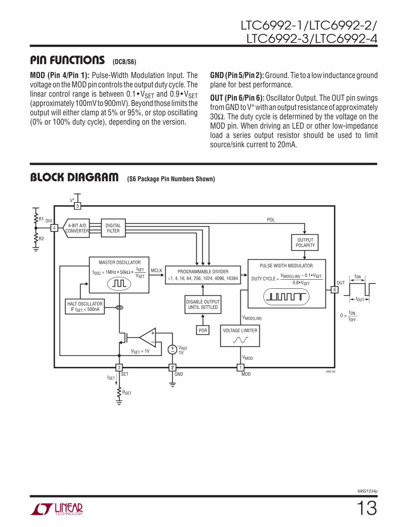
LTC6992-1/LTC6992-2/LTC6992-3/LTC6992-4
1369921234p
BLOCK DIAGRAM (S6 Package Pin Numbers Shown)
PIN FUNCTIONS (DCB/S6)
MOD (Pin 4/Pin 1): Pulse-Width Modulation Input. The voltage on the MOD pin controls the output duty cycle. The linear control range is between 0.1 • VSET and 0.9 • VSET (approximately 100mV to 900mV). Beyond those limits the output will either clamp at 5% or 95%, or stop oscillating (0% or 100% duty cycle), depending on the version.
GND (Pin 5/Pin 2): Ground. Tie to a low inductance ground plane for best performance.
OUT (Pin 6/Pin 6): Oscillator Output. The OUT pin swings from GND to V+ with an output resistance of approximately 30Ω. The duty cycle is determined by the voltage on the MOD pin. When driving an LED or other low-impedance load a series output resistor should be used to limit source/sink current to 20mA.
6992 BD
PROGRAMMABLE DIVIDER
÷1, 4, 16, 64, 256, 1024, 4096, 16384
MASTER OSCILLATOR
DISABLE OUTPUTUNTIL SETTLED
POR
OUTPUTPOLARITY
DIGITALFILTER
4-BIT A/DCONVERTER
fOSC = 1MHz • 50kΩ •ISET
VSET
POLR1
R2
DIV
V+
OUT
D = tON
tOFF
5
4
1
6
HALT OSCILLATORIF ISET < 500nA
MCLK
+
–
ISET
VSET = 1V+–
VREF1V
3 22
GNDSET MOD
RSET
DUTY CYCLE =VMOD(LIM) – 0.1•VSET
0.8•VSET
VOLTAGE LIMITER
VMOD(LIM)
VMOD
PULSE WIDTH MODULATOR
tOUT
tON

LTC6992-1/LTC6992-2/LTC6992-3/LTC6992-4
1469921234p
OPERATIONThe LTC6992 is built around a master oscillator with a 1MHz maximum frequency. The oscillator is controlled by the SET pin current (ISET) and voltage (VSET), with a 1MHz • 50k conversion factor that is accurate to ±0.8% under typical conditions.
fMASTER = 1
tMASTER
= 1MHz • 50k •ISET
VSET
A feedback loop maintains VSET at 1V ±30mV, leaving ISET as the primary means of controlling the output frequency. The simplest way to generate ISET is to connect a resistor (RSET) between SET and GND, such that ISET = VSET/RSET. The master oscillator equation reduces to:
fMASTER = 1
tMASTER
= 1MHz • 50k
RSET
From this equation it is clear that VSET drift will not affect the output frequency when using a single program resistor (RSET). Error sources are limited to RSET tolerance and the inherent frequency accuracy ΔfOUT of the LTC6992.
RSET may range from 50k to 800k (equivalent to ISET between 1.25μA and 20μA).
The LTC6992 includes a programmable frequency divider which can further divide the frequency by 1, 4, 16, 64, 256, 1024, 4096 or 16384 before driving the OUT pin. The divider ratio NDIV is set by a resistor divider attached to the DIV pin.
fOUT = 1
tOUT
= 1MHz • 50k
NDIV
•ISET
VSET
With RSET in place of VSET/ISET the equation reduces to:
fOUT =
1
tOUT
= 1MHz • 50k
NDIV •RSET
DIVCODE
The DIV pin connects to an internal, V+ referenced 4-bit A/D converter that monitors the DIV pin voltage (VDIV) to determine the DIVCODE value. DIVCODE programs two settings on the LTC6992:
1. DIVCODE determines the output frequency divider setting, NDIV.
2. DIVCODE determines the output polarity, via the POL bit.
VDIV may be generated by a resistor divider between V+ and GND as shown in Figure 1.
Figure 1. Simple Technique for Setting DIVCODE
6992 F01
LTC6992
V+
DIV
GND
R1
R2
2.25V TO 5.5V

LTC6992-1/LTC6992-2/LTC6992-3/LTC6992-4
1569921234p
Table 1 offers recommended 1% resistor values that ac-curately produce the correct voltage division as well as the corresponding NDIV and POL values for the recommended resistor pairs. Other values may be used as long as:
1. The VDIV/V+ ratio is accurate to ±1.5% (including resis-tor tolerances and temperature effects)
2. The driving impedance (R1||R2) does not exceed 500kΩ.
If the voltage is generated by other means (i.e. the output of a DAC) it must track the V+ supply voltage. The last
column in Table 1 shows the ideal ratio of VDIV to the supply voltage, which can also be calculated as:
VDIV
V+ = DIVCODE + 0.5
16 ±1.5%
For example, if the supply is 3.3V and the desired DIVCODE is 4, VDIV = 0.281 • 3.3V = 928mV ± 50mV.
Figure 2 illustrates the information in Table 1, showing that NDIV is symmetric around the DIVCODE midpoint.
Table 1. DIVCODE Programming
DIVCODE POL NDIV RECOMMENDED fOUT R1 (kΩ) R2 (kΩ) VDIV/V+
0 0 1 62.5kHz to 1MHz Open Short ≤0.03125 ±0.015
1 0 4 15.63kHz to 250kHz 976 102 0.09375 ±0.015
2 0 16 3.906kHz to 62.5kHz 976 182 0.15625 ±0.015
3 0 64 976.6Hz to 15.63kHz 1000 280 0.21875 ±0.015
4 0 256 244.1Hz to 3.906kHz 1000 392 0.28125 ±0.015
5 0 1024 61.04Hz to 976.6Hz 1000 523 0.34375 ±0.015
6 0 4096 15.26Hz to 244.1Hz 1000 681 0.40625 ±0.015
7 0 16384 3.815Hz to 61.04Hz 1000 887 0.46875 ±0.015
8 1 16384 3.815Hz to 61.04Hz 887 1000 0.53125 ±0.015
9 1 4096 15.26Hz to 244.1Hz 681 1000 0.59375 ±0.015
10 1 1024 61.04Hz to 976.6Hz 523 1000 0.65625 ±0.015
11 1 256 244.1Hz to 3.906kHz 392 1000 0.71875 ±0.015
12 1 64 976.6Hz to 15.63kHz 280 1000 0.78125 ±0.015
13 1 16 3.906kHz to 62.5kHz 182 976 0.84375 ±0.015
14 1 4 15.63kHz to 250kHz 102 976 0.90625 ±0.015
15 1 1 62.5kHz to 1MHz Short Open ≥0.96875 ±0.015
OPERATION
Figure 2. Frequency Range and POL Bit vs DIVCODE
0.5•V+
f OU
T (
kHz)
6992 F02
1000
100
10
1
0.001
0.1
0.01
INCREASING VDIV
V+0V
POL BIT = 0 POL BIT = 1
0 15
1
3
2
5
4
7
6 9
8
11
10
13
12
14

LTC6992-1/LTC6992-2/LTC6992-3/LTC6992-4
1669921234p
Pulse Width (Duty Cycle) Modulation
The MOD pin is a high impedance analog input providing direct control of the output duty cycle. The duty cycle is proportional to the voltage applied to the MOD pin, VMOD.
Duty Cycle = D =
VMOD
0.8 • VSET
− 1
8
The PWM duty cycle accuracy ΔD specifies that the above equation is valid to within ±4.5% for VMOD between 0.2 • VSET and 0.8 • VSET (12.5% to 87.5% duty cycle).
Since VSET = 1V ±30mV, the duty cycle equation may be approximated by the following equation.
Duty Cycle = D ≅
VMOD − 100mV
800mV
The VMOD control range is approximately 0.1V to 0.9V. Driving VMOD beyond that range (towards GND or V+) will have no further affect on the duty cycle.
Duty Cycle Limits
The only difference between the four versions of the LTC6992 is the limits, or clamps, placed on the output duty cycle. The LTC6992-1 generates output duty cycles ranging from 0% to 100%, meaning the output can stop oscillating and rest at GND or V+.
The LTC6992-2 will never stop oscillating, regardless of the VMOD level. Internal clamping circuits limit its duty cycle to a 5% to 95% range (1% to 99% guaranteed). Therefore, its VMOD control range is 0.14 • VSET to 0.86 • VSET (approximately 0.14V to 0.86V).
The LTC6992-3 and LTC6992-4 complete the family by providing one-sided clamping. The LTC6992-3 allows 0% to 95% duty cycle, and the LTC6992-4 allows 5% to 100% duty cycle.
Output Polarity (POL Bit)
The duty cycle equation describes a proportional transfer function, where duty cycle increases as VMOD increases. The LTC6992 includes a POL bit (determined by the DIVCODE as described earlier) that inverts the output signal. This makes the duty cycle gain negative, reducing duty cycle as VMOD increases.
OPERATION
Figure 3. POL Bit Functionality
6992 F03
OUT
POL = 1
tOUT
D•tOUT
OUT
POL = 0
tOUT
D•tOUT
DVMOD
0.8 • VSET
18
D 1VMOD
0.8 • VSET
18

LTC6992-1/LTC6992-2/LTC6992-3/LTC6992-4
1769921234p
POL = 1 forces a simple logic inversion, so it changes the duty cycle range of the LTC6992-3 (making it 100% to 5%) and LTC6992-4 (making it 95% to 0%). These transfer functions are detailed in Figure 4.
Table 2. Duty Cycle Ranges
PART NUMBER
DUTY CYCLE RANGE vs VMOD = 0V → 1V
POL = 0 POL = 1
LTC6992-1 0% to 100% 100% to 0%
LTC6992-2 5% to 95% 95% to 5%
LTC6992-3 0% to 95% 100% to 5%
LTC6992-4 5% to 100% 95% to 0%
OPERATION
Figure 4. PWM Transfer Functions for All LTC6992 Family Parts
VMOD/VSET (V/V)
0
DU
TY C
YC
LE (
%)
100
90
60
40
20
70
80
50
30
10
00.4 0.8 0.90.2 0.6
6992 F04a
VMOD/VSET = 0.9
VMOD/VSET = 0.1
10.3 0.70.1 0.5
POL = 1 POL = 0
VMOD/VSET (V/V)
0
DU
TY C
YC
LE (
%)
100
90
60
40
20
70
80
50
30
10
00.4 0.8 0.90.2 0.6
6992 F04b
10.3 0.70.1 0.5
POL = 1 POL = 0
VMOD/VSET = 0.86
VMOD/VSET = 0.14
VMOD/VSET (V/V)
0
DU
TY C
YC
LE (
%)
100
90
60
40
20
70
80
50
30
10
00.4 0.8 0.90.2 0.6
6992 F02c
10.3 0.70.1 0.5
POL = 1 POL = 0
VMOD/VSET = 0.1
VMOD/VSET = 0.86
VMOD/VSET (V/V)
0
DU
TY C
YC
LE (
%)
100
90
60
40
20
70
80
50
30
10
00.4 0.8 0.90.2 0.6
6992 F02d
10.3 0.70.1 0.5
POL = 1 POL = 0
VMOD/VSET = 0.9
VMOD/VSET = 0.14
LTC6992-1 LTC6992-2
LTC6992-3 LTC6992-4

LTC6992-1/LTC6992-2/LTC6992-3/LTC6992-4
1869921234p
Changing DIVCODE After Start-Up
Following start-up, the A/D converter will continue monitoring VDIV for changes. Changes to DIVCODE will be recognized slowly, as the LTC6992 places a priority on eliminating any “wandering” in the DIVCODE. The typical delay depends on the difference between the old and new DIVCODE settings and is proportional to the master oscillator period.
tDIVCODE = 16 • (ΔDIVCODE + 6) • tMASTER
A change in DIVCODE will not be recognized until it is stable, and will not pass through intermediate codes. A digital filter is used to guarantee the DIVCODE has settled to a new value before making changes to the output. Then the output will make a clean (glitchless) transition to the new divider setting.
OPERATIONStart-Up Time
When power is first applied to the LTC6992 the power-on reset (POR) circuit will initiate the start-up time, tSTART. The OUT pin is held low during this time. The typical value for tSTART ranges from 0.5ms to 8ms depending on the master oscillator frequency (independent of NDIV):
tSTART(TYP) = 500 • tMASTER
The output will begin oscillating after tSTART. If POL = 0 the first pulse has the correct width. If POL = 1 (DIVCODE ≥ 8), the first pulse width can be shorter or longer than expected, depending on the duty cycle setting, and will never be less than 25% of tOUT.
During start-up, the DIV pin A/D converter must determine the correct DIVCODE before the output is enabled. The start-up time may increase if the supply or DIV pin volt-ages are not stable. For this reason, it is recommended to minimize the capacitance on the DIV pin so it will properly track V+. Less than 100pF will not affect performance.
6992 F06
OUT
DIV STABLE VDIV
V+
tDIVCODE
tSTART
1ST PULSE WIDTH MAY BE INACCURATE
Figure 5. DIVCODE Change from 5 to 2 Figure 6. Start-Up Timing Diagram

LTC6992-1/LTC6992-2/LTC6992-3/LTC6992-4
1969921234p
Basic Operation
The simplest and most accurate method to program the LTC6992 is to use a single resistor, RSET, between the SET and GND pins. The design procedure is a four step process. After choosing the POL bit setting and proper LTC6992 version, select the NDIV value and then calculate the value for the RSET resistor.
Step 1: Selecting the POL Bit Setting
Most applications will use POL = 0, resulting in a positive transfer function. However, some applications may require a negative transfer function, where increasing VMOD reduces the output duty cycle. For example, if the LTC6992 is used in a feedback loop, POL = 1 may be required to achieve negative feedback.
Step 2: Selecting the LTC6992 Version
The difference between the LTC6992 versions is observed at the endpoints of the duty cycle control range. Applica-tions that require the output never stop oscillating should use the LTC6992-2. If it is better to allow the output to rest at GND or V+ (0% or 100% duty cycle, respectively), select the LTC6992-1.
The LTC6992-3 and LTC6992-4 clamp the duty cycle at only one end of the control range, allowing the output to stop oscillating at the other extreme. If POL = 1 the clamp will swap from low duty cycle to high, or vice-versa. Refer to Table 2 and Figure 4 for assistance in selecting the proper version.
Step 3: Selecting the NDIV Frequency Divider Value
As explained earlier, the voltage on the DIV pin sets the DIVCODE which determines both the POL bit and the NDIV value. For a given output frequency, NDIV should be selected to be within the following range.
62.5kHz
fOUT
≤ NDIV ≤ 1MHz
fOUT (1a)
To minimize supply current, choose the lowest NDIV value (generally recommended). For faster start-up or decreased jitter, choose a higher NDIV setting. Alternatively, use Table 1 as a guide to select the best NDIV value for the given ap-plication.
APPLICATIONS INFORMATIONWith POL already chosen, this completes the selection of DIVCODE. Use Table 1 to select the proper resistor divider or VDIV/V+ ratio to apply to the DIV pin.
Step 4: Calculate and Select RSET
The final step is to calculate the correct value for RSET
using the following equation.
RSET = 1MHz • 50k
NDIV • fOUT (1b)
Select the standard resistor value closest to the calculated value.
Example : Design a PWM circuit that satisfies the following requirements:
• fOUT = 20kHz
• Positive VMOD to duty cycle response
• Output can reach 100% duty cycle, but not 0%
• Minimum power consumption
Step 1: Selecting the POL Bit Setting
For positive transfer function (duty cycle increases with VMOD), choose POL = 0.
Step 2: Selecting the LTC6992 Version
To limit the minimum duty cycle, but allow the maximum duty cycle to reach 100%, choose LTC6992-4. (Note that if POL = 1 the LTC6992-3 would be the correct choice.)
Step 3: Selecting the NDIV Frequency Divider Value
Choose an NDIV value that meets the requirements of Equation (1a).
3.125 ≤ NDIV ≤ 50
Potential settings for NDIV include 4 and 16. NDIV = 4 is the best choice, as it minimizes supply current by us-ing a large RSET resistor. POL = 0 and NDIV = 4 requires DIVCODE = 1. Using Table 1, choose the R1 and R2 values to program DIVCODE = 1.

LTC6992-1/LTC6992-2/LTC6992-3/LTC6992-4
2069921234p
APPLICATIONS INFORMATIONStep 4: Select RSET
Calculate the correct value for RSET using Equation (1b).
RSET = 1MHz • 50k
4 • 20kHz= 625k
Since 625k is not available as a standard 1% resistor, substitute 619k if a 0.97% frequency shift is acceptable. Otherwise, select a parallel or series pair of resistors such as 309k and 316k to attain a more precise resistance.
The completed design is shown in Figure 7.
6992 F07
LTC6992-4
MOD
GND
SET
OUT
V+
DIV
R1976k
DIVCODE = 1
R2102k
RSET625k
VMOD
2.25V TO 5.5V
Figure 7. 20kHz PWM Oscillator
Figure 8. Duty Cycle Variation Due to ΔVSET
VMOD (V)
0
DU
TY C
YC
LE (
%)
100
90
70
80
60
50
30
40
20
10
00.60.2
6992 F08
10.4 0.8
ΔVSET = 0mV
ΔVSET = 30mV
ΔVSET = –30mV
Figure 9. Fixed-Frequency, Arbitrary Duty Cycle Oscillator
6992 F09
LTC6992-X
MOD
GND
SET
OUT
V+
DIV
R1
R2
RSET2
RSET1
2.25V TO 5.5V
D54
•RSET2
RSET1 RSET2
18
Some applications can eliminate ΔVSET sensitivity by making VMOD proportional to VSET. For example, Figure 9 shows a simple circuit for generating an arbitrary duty cycle. The equation for duty cycle does not depend on VSET at all.
Duty Cycle Sensitivity to ΔVSET
The output duty cycle is proportional to the ratio of VMOD/VSET. Since VSET can vary up to ±30mV from 1V it can effectively gain or attenuate VMOD, as shown below when ΔVSET is added to the equation.
D =VMOD
0.8 • VSET + ΔVSET( ) − 1
8
The simplifying assumption of ΔVSET = 0V creates the po-tential for additional duty cycle error, which increases with VMOD, reaching a maximum of 3.4% if ΔVSET = –30mV.
ΔD ≅
VMOD
800mV•
ΔVSET
VSET
≅ − Dideal + 1
8⎛⎝⎜
⎞⎠⎟ •
ΔVSET
VSET
Figure 8 demonstrates the worst-case impact of this varia-tion (if VSET is at its 0.97V or 1.03V limits).
This error is in addition to the inherent PWM duty cycle accuracy spec ΔD (±4.5%), so care should be taken if ac-curacy at high duty cycles (VMOD near 0.9V) is critical.
ISET Extremes (Master Oscillator Frequency Extremes)
Pushing ISET outside of the recommended 1.25μA to 20μA range forces the master oscillator to operate outside of the 62.5kHz to 1MHz range in which it is most accurate.
The oscillator will still function with reduced accuracy for ISET < 1.25μA. At approximately 500nA, the oscillator output will be frozen in its current state. The output could halt in a high or low state. This avoids introducing short pulses while frequency modulating a very low frequency output.

LTC6992-1/LTC6992-2/LTC6992-3/LTC6992-4
2169921234p
APPLICATIONS INFORMATIONAt the other extreme, it is not recommended to operate the master oscillator beyond 2MHz because the accuracy of the DIV pin ADC will suffer.
Pulse Width Modulation Bandwidth and Settling Time
The LTC6992 will respond to changes in VMOD up to a –3dB bandwidth of TBD (see Figure 10). This makes it easy to stabilize a feedback loop around the LTC6992, since it does not introduce a low frequency pole.
Duty cycle settling time depends on the master oscillator frequency. Following a ±100mV step change in VMOD, the duty cycle takes approximately TBD master clock cycles
(TBD • tMASTER) to settle to within 1% of the final value. An example is shown in Figure 11.
Frequency Modulation and Settling Time
In addition to pulse-width modulation, the LTC6992 can be frequency modulated by varying ISET. The LTC6992 will respond to changes in ISET up to a –3dB bandwidth of TBD • fOUT (see Figure 12).
Following a 2x or 0.5x step change in ISET, the output frequency takes approximately TBD master clock cycles (TBD • tMASTER) to settle to within 1% of the final value. An example is shown in Figure 13.
Figure 13. Frequency Change Settling Time
PLACEHOLDER
Figure 10. PWM Frequency Response
Figure 11. PWM Settling Time
Figure 12. Frequency Modulation Bandwidth
PLACEHOLDER
PLACEHOLDER
PLACEHOLDER

LTC6992-1/LTC6992-2/LTC6992-3/LTC6992-4
2269921234p
Power Supply Current
The power supply current varies with frequency, supply voltage and output loading. It can be estimated under any condition using the following equation:
If NDIV = 1 (DIVCODE = 0 or 15):
IS(TYP) ≈ V+ • fOUT • 39pF + CLOAD( )
L+ V+
320kΩ+ V+
2 •RLOAD
+ 2.2 •ISET + 85µA
If NDIV > 1 (DIVCODE = 1 or 14):
IS(TYP) ≈ V+ •fOUT
NDIV
• 27pF + V+ • fOUT • 27pF + CLOAD( )
L+ V+
320kΩ+ V+
2 •RLOAD
+ 2.6 •ISET + 90µA
SUPPLY BYPASSING AND PCB LAYOUT GUIDELINES
The LTC6992 is a 2.4% accurate silicon oscillator when used in the appropriate manner. The part is simple to use and by following a few rules, the expected performance is easily achieved. The most important use issues involve adequate supply bypassing and proper PCB layout.
Figure 14 shows example PCB layouts for both the TSOT-23 and DFN packages using 0603 sized passive components. The layouts assume a two layer board with a ground plane layer beneath and around the LTC6992. These layouts are a guide and need not be followed exactly.
APPLICATIONS INFORMATION1. Connect the bypass capacitor, C1, directly to the V+ and
GND pins using a low inductance path. The connection from C1 to the V+ pin is easily done directly on the top layer. For the DFN package, C1’s connection to GND is also simply done on the top layer. For the TSOT-23, OUT can be routed through the C1 pads to allow a good C1 GND connection. If the PCB design rules do not allow that, C1’s GND connection can be accomplished through multiple vias to the ground plane. Multiple vias for both the GND pin connection to the ground plane and the C1 connection to the ground plane are recommended to minimize the inductance. Capacitor C1 should be a 0.1μF ceramic capacitor.
2. Place all passive components on the top side of the board. This minimizes trace inductance.
3. Place RSET as close as possible to the SET pin and make a direct, short connection. The SET pin is a current summing node and currents injected into this pin directly modulate the operating frequency. Having a short connection minimizes the exposure to signal pickup.
4. Connect RSET directly to the GND pin. Using a long path or vias to the ground plane will not have a significant affect on accuracy, but the direct, short connection is recommended and easy to apply.
5. Use a ground trace to shield the SET pin. This provides another layer of protection from radiated signals.
6. Place R1 and R2 close to the DIV pin. A direct, short connection to the DIV pin minimizes the external signal coupling.

LTC6992-1/LTC6992-2/LTC6992-3/LTC6992-4
2369921234p
TYPICAL APPLICATIONS
Figure 14. Supply Bypassing and PCB Layout
Constant On-Time Modulator
6992 TA02
LTC6992-1
MOD
GND
SET
OUT
V+
DIV
RM29.31k
RM11.05k
RSET44.2k
RIN*11.8k VCTRL
VMOD
VSET
VIN0V TO 2V R1
182kDIVCODE = 2(÷16, POL = 1)
C10.1μF
OUT
R2976k
VCC
*OPTIONAL RESISTOR ADJUSTS FOR DESIRED VIN RANGE.
AS VIN INCREASES, tOUT INCREASES AND DUTY CYCLE DECREASES (BECAUSE POL = 1) TO MAINTAIN A CONSTANT tON.FOR CONSTANT OFF-TIME, JUST CHANGE DIVCODE SO POL = 0.
IFRM2
RM1+RM20.9 THEN tON = NDIV • 1.125μs •
RSET
50k
APPLICATIONS INFORMATION
6992 F14
LTC6992
MOD
GND
SET
OUT
V+
DIV
C10.1μF R1
R2RSET
V+
MOD
GND
SET
OUT
V+
DIV
V+
DIV
SET
OUT
GND
MOD
R1
R2
C1
RSET
V+C1R1
R2
V+
RSET
TSOT-23 PACKAGEDFN PACKAGE

LTC6992-1/LTC6992-2/LTC6992-3/LTC6992-4
2469921234p
TYPICAL APPLICATIONSDigitally Controlled Duty Cycle with Internal VREF Reference Variation Eliminated
Programming NDIV Using an 8-Bit DAC
6992 TA03
LTC6992-X
MOD
GND
SET
OUT
V+
DIV
RSET
–
+
V+
1/2LTC6078
R1
C10.1μF
R2
LTC1659VOUT CLK μP
CS/LD
DIN
REF VCC
GND
V+
V+
6992 TA04
LTC6992-X
MOD
GND
SET
OUT
V+
DIV
RSET
C10.1μF
LTC2630-LZ8VOUT SCK μP
CS/LD
SDIVCC
GND
2.25V TO 5.5V
C20.1μF
DIVCODE
0123456789101112131415
DAC CODE
02440567288104120136152168184200216232
≥255
ANALOG PWMDUTY CYCLE CONTROL
(0V TO 1V)

LTC6992-1/LTC6992-2/LTC6992-3/LTC6992-4
2569921234p
TYPICAL APPLICATIONSChanging Between Two Frequencies
6992 TA05
LTC6992-X
MOD
GND
SET
OUT
V+
DIV
R1
R2RSET
V+
NOTESWHILE THIS CIRCUIT IS SIMPLER THAN THE CIRCUIT TO THE RIGHT, ITS FREQUENCY ACCURACY IS WORSE DUE TO THE EFFECT OFV+ SUPPLY VARIATION FROM SYSTEM TO SYSTEM AND OVER TEMPERATURE.
NOTES1. WHEN THE NMOSFET IS OFF, THE FREQUENCY IS SET BY RSET = RSET1.2. WHEN THE NMOSFET IS ON, THE FREQUENCY IS SET BY RSET = RSET1 || RSET2.3. V+ SUPPLY VARIATION IS NOT A FACTOR AS THE SWITCHING RESISTOR IS EITHER FLOATING OR CONNECTED TO GROUND.
RVCO
V+
‘HC04
fMAX
fMIN
ANALOG PWMDUTY CYCLE CONTROL
(0V TO 1V)LTC6992-X
MOD
GND
SET
OUT
V+
DIV
R1
R2RSET1RSET2
V+
ANALOG PWMDUTY CYCLE CONTROL
(0V TO 1V)
V+
‘HC042N7002
fMIN
fMAX
Simple Diode Temperature Sensor
6992 TA06
LTC6992-2
MOD
GND
SET
OUT
V+
DIV
R41000k
MOC207M
Q1
OUTPUT
D3
C11μF
R5186k
5V
5V5V
LT6003
+10mV/C
5V
R1130k
R250k
R3130k
ADJUST FOR 50% DUT CYCLE AT 25°C
+
–R7
16.9k
R884.5k
R645.3k
D11N458
R11422Ω
NDIV = 16f = 10kHz
PWM OUTPUT FOR ISOLATED MEASUREMENT+1% DUTY CYCLE CHANGE PER DEGREE C–10°C TO 65°C RANGE WITH OPTO-ISOLATOR (DC: 15% TO 95%)
R9365Ω

LTC6992-1/LTC6992-2/LTC6992-3/LTC6992-4
2669921234p
Motor Speed/Direction Control for Full H-Bridge (Locked Anti-Phase Drive)
TYPICAL APPLICATIONS
6992 TA07
LTC6992-2
MOTOR
A1
A2
CW CURRENTFLOW
VS12V
POWER H-BRIDGEHIGH = SWITCH ON
MOD
GND
SET
OUT
V+
DIV
R11000k
INPUT 0V TO 1V
R2280k
V+
R3300k
2.6kHz, 5% TO 95% PWM5% DC = CLOCKWISE50% DC = STOPPED95% DC = COUNTER CLOCKWISE
Motor Speed/Direction Control for Full H-Bridge (Sign/Magnitude Drive)
6992 TA08
LTC6992-2
MOTOR
A3
A4 A5
CW CURRENTFLOW
VS12V
POWER H-BRIDGEHIGH = SWITCH ON
MOD
GND
SET
OUT
V+
DIV
R41000k
INPUT 0V TO 1V
R5280k
V+
R3300k
2.6kHz, 5% TO 95% PWM5% DC = SLOW95% DC = FAST
DIRECTIONH = CCW, L = CW

LTC6992-1/LTC6992-2/LTC6992-3/LTC6992-4
2769921234p
TYPICAL APPLICATIONSRatiometric Sensor to Pulse Width, Non-Inverting Response
6992 TA09
LTC6992-1
C10.15μF
MOD
GND
SET
OUT
V+
DIV
R11000k
R2186k
VS
OUTPUTDUTY CYCLE = K • 100%
VS
LT1490K • VS
2.5V TO 5.5V
RSET316k
+
–R310kK = 1
K = 0
R490.9k
R510M
R69.09k
RSENSOR
NDIV = 16fOUT = 10kHz
C20.22μF
Ratiometric Sensor to Pulse Width, Inverting Response
6992 TA10
LTC6992-1
C10.15μF
MOD
GND
SET
OUT
V+
DIV
R11000k
R2186k
VS
OUTPUTDUTY CYCLE = (1–K) • 100%
VS
VS
VS
LT1490
2.5V TO 5.5V
RSET316k
+
–
R3100k
R410k
K = 1
K = 0
R690.9k
K • VS
R510k
R69.09k
RSENSOR
NDIV = 16fOUT = 10kHz
C20.22μF

LTC6992-1/LTC6992-2/LTC6992-3/LTC6992-4
2869921234p
TYPICAL APPLICATIONSRatio Control Servo Pulse Generator
6992 TA11
LTC6992-1
C11μF
MOD
GND
SET
OUT
V+
DIV
R11000k
R2681k
VS
OUTPUT1ms TO 2ms PULSE EVERY 16ms
VS
VS
LT1490
2.5V TO 5.5V
RSET316k
+
–
R690.9k
R5130k
R68.66k
SERVOCONTROLPOT10k
2ms
1ms
R69.09k
NDIV = 4096fOUT = 62.5kHz, 16ms PERIOD
C20.22μF
Direct Voltage Controlled PWM Dimming 0 to 15000 Cd/m2 Intensity
6992 TA12
LTC6992-1
MOD
GND
SET
OUT
V+
DIV
f = 7.5kHzNDIV = 64
5VD1
HIGH INTENSITY LEDSSL-LX5093XUWC
R2280k
RSET105k
VDIMMING
R11M
R390.9Ω
C10.1μF

LTC6992-1/LTC6992-2/LTC6992-3/LTC6992-4
2969921234p
TYPICAL APPLICATIONSWide Range LED Dimming (0 to 85000 Cd/m2 Brightness)
6992 TA13
LTC6992-4
MOD
GND
SET
OUT
V+
DIV
RDIV11M
RDIV2280k
5V
5V
LT6004
RSET161.9k
+
–
5V
LT6004
+
–
R310k
VREF
VFAST
R47.5k
VDIMMING0V TO 1.65V
VSLOW
R27.5k
R110k
5–100%NDIV = 64f = 12.6kHz
0–100%NDIV = 4096fOUT = 100kHz
SLOW PWMCONTROLS 0 TO 6000Cd/m2 BRIGHTNESS
FAST PWMCONTROLS 6000 TO 85000
Cd/m2 BRIGHTNESS
C40.1μF
LTC6992-1
MOD
GND
SET
OUT
V+
DIV
RDIV31M
RDIV4681k
5V
3.3V 5V
RSET2124k
C10.1μF
3.3VIN PVIN
PWM
A1 D1
D2
LUMILEDS LXHL-BW02
LT3518UF
LED+

LTC6992-1/LTC6992-2/LTC6992-3/LTC6992-4
3069921234p
DCB Package6-Lead Plastic DFN (2mm × 3mm)
(Reference LTC DWG # 05-08-1715 Rev A)
PACKAGE DESCRIPTION
3.00 ±0.10(2 SIDES)
2.00 ±0.10(2 SIDES)
NOTE:1. DRAWING TO BE MADE A JEDEC PACKAGE OUTLINE M0-229 VARIATION OF (TBD)2. DRAWING NOT TO SCALE3. ALL DIMENSIONS ARE IN MILLIMETERS4. DIMENSIONS OF EXPOSED PAD ON BOTTOM OF PACKAGE DO NOT INCLUDE MOLD FLASH. MOLD FLASH, IF PRESENT, SHALL NOT EXCEED 0.15mm ON ANY SIDE5. EXPOSED PAD SHALL BE SOLDER PLATED 6. SHADED AREA IS ONLY A REFERENCE FOR PIN 1 LOCATION ON THE
TOP AND BOTTOM OF PACKAGE
0.40 ± 0.10
BOTTOM VIEW—EXPOSED PAD
1.65 ± 0.10(2 SIDES)
0.75 ±0.05
R = 0.115TYP
R = 0.05TYP
1.35 ±0.10(2 SIDES)
13
64
PIN 1 BARTOP MARK
(SEE NOTE 6)
0.200 REF
0.00 – 0.05
(DCB6) DFN 0405
0.25 ± 0.050.50 BSC
PIN 1 NOTCHR0.20 OR 0.25 × 45° CHAMFER
0.25 ± 0.05
1.35 ±0.05(2 SIDES)
RECOMMENDED SOLDER PAD PITCH AND DIMENSIONS
1.65 ±0.05(2 SIDES)
2.15 ±0.05
0.70 ±0.05
3.55 ±0.05
PACKAGEOUTLINE
0.50 BSC

LTC6992-1/LTC6992-2/LTC6992-3/LTC6992-4
3169921234p
Information furnished by Linear Technology Corporation is believed to be accurate and reliable. However, no responsibility is assumed for its use. Linear Technology Corporation makes no representa-tion that the interconnection of its circuits as described herein will not infringe on existing patent rights.
PACKAGE DESCRIPTIONS6 Package
6-Lead Plastic TSOT-23(Reference LTC DWG # 05-08-1636 Rev B)
1.50 – 1.75(NOTE 4)
2.80 BSC
0.30 – 0.45 6 PLCS (NOTE 3)
DATUM ‘A’
0.09 – 0.20(NOTE 3) S6 TSOT-23 0302 REV B
2.90 BSC(NOTE 4)
0.95 BSC
1.90 BSC
0.80 – 0.90
1.00 MAX0.01 – 0.10
0.20 BSC
0.30 – 0.50 REF
PIN ONE ID
NOTE:1. DIMENSIONS ARE IN MILLIMETERS2. DRAWING NOT TO SCALE3. DIMENSIONS ARE INCLUSIVE OF PLATING4. DIMENSIONS ARE EXCLUSIVE OF MOLD FLASH AND METAL BURR5. MOLD FLASH SHALL NOT EXCEED 0.254mm6. JEDEC PACKAGE REFERENCE IS MO-193
3.85 MAX
0.62MAX
0.95REF
RECOMMENDED SOLDER PAD LAYOUTPER IPC CALCULATOR
1.4 MIN2.62 REF
1.22 REF

LTC6992-1/LTC6992-2/LTC6992-3/LTC6992-4
3269921234p
Linear Technology Corporation1630 McCarthy Blvd., Milpitas, CA 95035-7417 (408) 432-1900 FAX: (408) 434-0507 www.linear.com © LINEAR TECHNOLOGY CORPORATION 2010
LT 0510 • PRINTED IN USA
RELATED PARTS
TYPICAL APPLICATION
PART NUMBER DESCRIPTION COMMENTS
LTC1799 1MHz to 33MHz ThinSOT Silicon Oscillator Wide Frequency Range
LTC6900 1MHz to 20MHz ThinSOT Silicon Oscillator Low Power, Wide Frequency Range
LTC6906/LTC6907 10kHz to 1MHz or 40kHz ThinSOT Silicon Oscillator Micropower, ISUPPLY = 35μA at 400kHz
LTC6990 TimerBlox, Voltage Controlled Oscillator Frequency from 488Hz to 1MHz, No Caps, 2% Accurate
LTC6991 TimerBlox, Very Low Frequency Clock with Reset Cycle Time from 2ms to 9.5 Hours, No Caps, 2% Accurate
LTC6993-1 TimerBlox, Monostable Pulse Generator Resistor Set Pulse Width from 1μs to 2ms, No Caps, 2% Accurate
LTC6993-2 TimerBlox, Retriggerable Monostable Pulse Generator Resistor Set Pulse Width from 1μs to 2ms, No Caps, 2% Accurate
LTC6994-1 TimerBlox, Delay Block, First Edge Only Delayed Resistor Set Delay from 1μs to 2ms, No Caps, 2% Accurate
LTC6994-2 TimerBlox, Delay Block/Debouncer, Both Edges Delayed Resistor Set Delay from 1μs to 2ms, No Capacitors Required, 2% Accurate
LED Driver with 5000:1 Dimming Range
6992 TA14
LTC6992-1
MOD
GND
SET
OUT
V+
DIV
1M
681k102k
VIN5V TO 16V
ANALOG PWMDUTY CYCLE
CONTROL(0V TO 1V) 5V
LT3517
PWM
TGEN
VREF
CTRL
SYNC
FB
ISP
ISN
TG
SHDN VIN SW
VC GNDSSRT
C12.2μF
R13.92M
R2124k 300mA
C10.22μF
C24.7μF
C30.1pF
C40.1pF RT
6.04k2MHz
D1L1
6.8μH
LT3517
RSENSE330mΩ
C1: KEMET C0806C225K4RACC2: KEMET C1206C475K3RACC3, C4: MURATA GRM21BR71H104KA01BC5: MURATA GRM21BR71H224KA01BD1: DIODE DFL5160L1: TOKO B992A5-6RBNLEDS: LUXEON I (WHITE)M1: ZETEX ZXMP6A13FTA