Status of the hard X-ray microprobe beamline ID22 of the European Synchrotron Radiation Facility
Upload
khangminh22Category
view
1download
0


Synchrotron Radiation in Natural Science Vol. 8, No. 1 – 2 (2009)
EDITORIAL
In this issue of Synchrotron Radiation in Natural
Science the readers will find the abstracts of the KSUPS-
8 (8th National Symposium of Synchrotron Users). The
abstracts are preceded by a description of the Polish FEL
project and memories of the early work at synchrotrons
in mid 1980s. Brief information on the Polish
synchrotron project is also included (pp. 41-42); more
details have been given in previous issues. Both
mentioned projects, of synchrotron and FEL, are at
different stages of processing. The way to acceptation of
the projects of this kind is typically long and meets many
obstacles, as illustrated e.g. by Olof Hallonsten's [1] for
the cases of MAXlab, ESRF and Stanford laboratories.
Many more or less obvious factors account in the
decision and choice of machine location and parameters.
The cost of the machine is not so high (being comparable
with the cost of a stadium or 10 km of a highway).
Another important factor is a creation, in advance, of a
lobby of a convincing power being able to reach the
decision makers with the message about the mission of
natural science for both, the society and for the
technology. Understanding that modern light sources
became a basic scientists' tool, and that their lack
enhances the brain drain, a natural process causing that
young people who learn the modern material
characterisation techniques do not find job in their native
countries, is a key point during the decision process.
Moreover, it is worth noting that at the turn of the
century, intense light sources started their work in
relatively small countries such as Sweden, Switzerland
and Singapore—the success of these scientific centres is
well known and will, certainly, encourage other countries
to follow the same way.
Thanks to the special programs of European
Commission so called I3 (Integrated Infrastructure
Initiative) scientists across Europe benefit from easier
access to Europe’s best synchrotron and free electron
laser facilities. The main objective of this program is the
support of the transnational open access to the
synchrotrons and FELs facilities, for users from the
European area. Under the 6th Framework Programme
(FP6) the Integrating Activity on Synchrotron and Free
Electron Laser Science (IA-SFS) project was active. The
duration of the project was 5 years: from March 1st, 2004
to February 28th, 2009, and the total EU support was at
the level of 27 million euro. Starting from March 2009,
the ELISA project is supported by the European
Community - Research Infrastructure Action under the
FP7 Programme [2]. It is the follow-up of a previous I3
[3]. The duration of the project is 30 months: March 1st,
2009 - August 31st, 2011, but the funds are only 10
million €, i.e. they are three times smaller than those got
within the FP6 programme. Moreover, there is a
discussion for further reduction and releasing the funding
responsibility completely to national funding agencies. A
special action should be taken to convince authorities
from Brussels that this is not a right way and such
politics can stress on the level of science in Europe and
ruin the many years' efforts to build the international
users community. In this aspect the users' voice should be
heard. The synchrotron facilities have sent a letter to the
users asking for filling a questionnaire to express their
concern about need for European Commission support
(see p. 99). This letter has been sent to 22000 e-mail
addresses of the users but only 1100 answers were
obtained through the webpage. The more actions are
needed. At p. 100 you will find a Manifest prepared by
an ad-hoc committee for a European Synchrotron User
Organization (ESUO) describing the present situation
with the proposition to perform activities which are very
important for our future access to national facilities.
We are pleased to inform the readers that Prof.
Krystyna Jablonska was elected by the ELISA Council as
one of user delegates in the Council (the remaining ones
are: Maria Arménia Carrondo, Keijo Hämäläinen, Ullrich
Pietsch and Marc Vrakking). The user delegates will
represent the users in the ELISA Council with mission of
supporting the transnational open access of users to the
synchrotrons and FELs facilities; developing innovative
instrumentation and techniques, enhancing the
communication between the consortium members and
strengthening the links to the general public.
References
[1] O. Hallonsten, Small science on big machines, PhD thesis ,
http://www.lu.se/o.o.i.s?id=12683&postid=1419054, (Lund
Univ. 2009).
[2] http://www.elettra.eu/ELISA/.
[3] http://www.elettra.trieste.it/I3/.
I

Contents / Synchrotron Radiation in Natural Science Vol. 8, No. 1-2 (2009)
II
CONTENTS
Editorial I
Synchrotron Light News 1
Regular contributions
G. Wrochna, J. Jagielski, J. Krzywiński, R. Nietubyć, J. Pełka, E. Pławski, J. Sekutowicz, R. Sobierajski, J. Szewiński
On the POLFEL free electron laser project 3
W. Kwiatek It all started out innocently enough… 8
M. Stankiewicz My first encounter with synchrotron. 34 years ago 15
KSUPS-8 8. Krajowe Sympozjum Użytkowników Promieniowania Synchrotronowego
KSUPS-8 - 8th National Symposium of Synchrotron Users
Programme of 8th National Symposium of Synchrotron Users 20
A. Burian, J. Szade Zaproszenie na 8. Krajowe Sympozjum Użytkowników Promieniowania Synchrotronowego
Welcome to 8th National Symposium of Synchrotron Users
22
KSUPS-8: invited lectures and oral presentations
T. Durakiewicz Synchrotron quest for band renormalization in correlated f-electron systems
L01 23
W.M. Kwiatek, M. Podgórczyk, C. Paluszkiewicz, M. Gajda, Z. Stachura, M. Lekka, J. Lekki, M. Piccinini, D. Grolimund
Novel microscopy methods of medical imaging L02 24
L. Chow, A. Misiuk, C.W. Pao, D.C. Ling, W.F. Pong, J. Bak-Misiuk
Synchrotron radiation study of Mn implanted silicon O01 25
A. Wierzbicka, D. Lübbert, J.Z. Domagała, Z.R. Żytkiewicz
Rocking curve imaging studies of latelarly overgrown GaAs and GaSb epitaxial layers
O02
ext
26
K. Wieteska, W. Wierzchowski, A. Malinowska, S. Turczyński, M. Lefeld-Sosnowska, D. Pawlak, T. Łukasiewicz, W. Graeff
X-ray topographic investigations of domain structure in Czochralski grown PrxLa1-xAlO3 crystals
O03 28
G. Wrochna, J. Jagielski, J. Krzywiński, R. Nietubyć, J. Pełka, E. Pławski, J. Sekutowicz, R. Sobierajski, J. Szewiński
POLFEL – the high average power free electron laser L03 29
J.B. Pełka, G. Wrochna, R. Nietubyć, K.R. Tybor
Applications of free electron lasers in biology and edicine O04 30
R. Sobierajski, M. Jurek, D. Klinger, A.R. Khorsand, E. Louis, S. Bruijn, R. van de Kruijs, E.D. van Hattum, K. Sokolowski-Tinten, U. Shymanovich, S. Toleikis, H. Wabnitz, K. Tiedtke, N. Stojanovic, L. Juha, J. Chalupsky, J. Cihelka, V. Hajkova, E.M. Gullikson, F. Bijkerk
Interaction of multilayer optics with intense femtosecond XUV pulses
O05 31

Contents / Synchrotron Radiation in Natural Science Vol. 8, No. 1-2 (2009)
P. Zajdel, I. Kruk, P.-Y. Hsieh, W. van Beek,M.A. Green
Local and long range orders in transition metal oxidesand selenides and metal organic frameworks studied usingcombined techniques (XRD and in-situ Raman)
L04 32
M. Sikora Study of magnetism with XMCD and XES L05 33
K. Lawniczak-Jablonska, A. Wolska,M.T. Klepka, J. Sadowski, A. Barcz,A. Hallen, D. Arvanitis
Charakteryzacja nano-wydzieleń w matrycach na bazie GaSb
Characterisation of nanoinclusions in GaSb-based matrices
L06
ext
34
M. Kozak Small angle scattering of synchrotron radiation studiesof biomembranes
L07 36
S. Krzywda, W. Białek, A. Szczepaniak,M. Jaskólski
Atomic-resolution structure of cyanobactrial cytochrome c6with an unusual sequence insertion
L08 37
H. Drozdowski, A. Romaniuk, Z. Błaszczak Short−range ordering in ortho−chloroanisole at 293 K by x−raydiffraction
O06 38
K. Mazur, W. Wierzchowski, K. Wieteska,W. Hofman, K. Kościewicz, W. Strupiński,W. Graeff
X-ray reflectometric investigation of surface roughnes of SiCsubstrate wafers and its influence on the structural perfectionof the deposited SiC epitaxial layers
O07 39
R. Przeniosło Badania struktury tlenków metali przejściowych metodądyfrakcji neutronów i promieniowania synchrotronowego
Studies of structure of transition metal oxideswith the methods of neutron diffraction and synchrotronradiation
L09 40
E.A. Görlich, K. Królas, M. Młynarczyk,M.J. Stankiewicz, K. Tomala
Informacja na temat rozwiązań technicznych i stanuprzygotowań do budowy synchrotronu w Polsce
Information on technical solutions and preparations tosynchrotoron construction in Poland
41
J. Szade, B. Orłowski, B. Kowalski,E.A. Görlich, K. Tomala, P. Starowicz
Pierwsza linia na polskim synchrotronie – spektroskopiemiękkiego promieniowania rentgenowskiego
First beamline at the Polish synchrotron: Spectroscopiesof soft X-rays
42
KSUPS-8: poster presentations
M. Kowalik, R. Zalecki, A. Kołodziejczyk Electronic states of collosal magnetoresistive manganitesLa0.67Pb0.33Mn1-xFexO3 from photoemission spectroscopy
P01 43
A. Malinowska, E. Wierzbicka,M. Lefeld-Sosnowska, K. Wieteska,W. Wierzchowski, T. Łukasiewicz,M. Świrkowicz, W. Graeff
Defect structure formed at different stages of growth processin erbium, calcium and holmium doped YVO4 crystals
P02 44
M. Szczerbowska-Boruchowska,M. Lankosz, A. Smykla, D. Adamek
Synchrotron radiation as a tool of biochemical analysis in braincancers
P03 45
J. Wolny, M. Duda, B. Kozakowski Complex structure of Mg2Al3 β and β’ phases P04 46
E. Dynowska, W. Szuszkiewicz, C. Ziereis,J. Geurts, S. Müller, C. Ronning,J. Domagala, P. Romanowski, W. Caliebe
Structural studies of heavily transition metal implanted ZnO P05 47
H. Grigoriew, L. Wiegert, A. Boczkowska Dynamic SAXS correlation as method of structural research P06 48
M.T. Klepka, K. Lawniczak-Jablonska,A. Wolska
Badania absorpcyjne zmodyfikowanych chemiczniechitozanów z żelazem
Absorption studies of chemically modified Fecontainingchitosans
P07 49
III

Contents / Synchrotron Radiation in Natural Science Vol. 8, No. 1-2 (2009)
A. Wolska, K. Lawniczak-Jablonska,M.T. Klepka, A. Barcz, A. Hallen,D. Arvanitis
Lokalne otoczenie jonów manganu implantowanychw kryształach GaSb
Local environment of manganese ions implanted into GaSbcrystals
P08
ext
50
A. Wolska, K. Lawniczak-Jablonska,M.T. Klepka, J. Sadowski
Wytrącenia MnSb w matrycy GaSb wytwarzane przy pomocymetody MBE
MnSb precipitates in GaSb matrix, produced using the MBEmethhod
P09
ext
52
J. Bak-Misiuk, P. Romanowski,E. Dynowska, J.Z. Domagala,J. Sadowski,T. Wojciechowski, R. Jakiela,W. Wierzchowski, K. Wieteska, W. Caliebe,W. Graeff
Defect structure of GaMnSb grown on GaAs substrate P10 54
A. Misiuk, W. Wierzchowski, K. Wieteska,J. Bak-Misiuk, B. Surma, A. Wnuk,C.A. Londos, Deren Yang, W. Graeff
Defect structure of Czochralski grown nitrogen doped siliconannealed under enhanced pressure
P11 55
D. Klinger, R. Sobierajski, M. Jurek,J. Krzywinski, J.B. Pelka, D. Żymierska,J. Chalupský, L. Juha, V. Hájková,J. Cihelka, T. Burian, L. Vyšín, H. Wabnitz,K. Tiedtke, S. Toleikis, T. Tschentscher,R. London, S. HauRiege, K. Sokolowski-Tinten, N. Stojanovic, J. Hajdu,A.R. Khorsand, A.J. Gleeson
Modification of the surface morphology by ultra short pulsesof XUV free electron laser
P12 56
P. Kuczera, B. Kozakowski, J. Wolny,R. Strzałka
Structure refinement of decagonal quasicrystal P13 57
J. Nowak, R. Chałas, J. Lekki, A. KuczumowMicrospectrometric study of internal structure of dentin-enamelboundary (DEJ) in molar teeth
P14 58
W. Nowicki, J. Darul, P. Piszora, T. Trots Structural properties of (Mn1-xFex)2O3 solid solutions P15 59
A. Pietnoczka, R. Bacewicz, M. Pękała,V. Drozd, W. Zalewski, J. Antonowicz
Local structure of Mn in (La1-xHox)2/3Ca1/3MnO3 using X-rayabsorption fine structure
P16 60
P. Piszora, J. Darul, W. Nowicki, C. Lathe Diffraction HP/HT study of LiMn2O4 P17 61
P. Romanowski, J. Bak-Misiuk,E. Dynowska, J. Sadowski,T. Wojciechowski, A. Barcz, R. Jakiela,W. Caliebe
Structural properties of high-temperature-grown GaMnSb /GaSb
P18 62
P. Seremak-Peczkis, W. Zajączkowski,J. Przewoźnik, Cz. Kapusta, M. Sikora,D.A. Zając, P. Pasierb, M. Bućko, M. Rękas
XAFS study and crystallographic structure of Ti and Y dopedBaCeO3-δ protonic conductors
P19 63
J. Stępień, J. Śliwińska, J. Przewoźnik,K. Schneider, Cz. Kapusta, D. Zajac,K. Michałów, D. Pomykalska, M. Bućko,M. Rękas
XAFS study of ZrO2–based SOFC materials P20 64
T. Balcer, W. Wierzchowski The simulation of Bragg-case section images of dislocationsand inclusions in aspect of identification of defects in SiCcrystals
P21 65
W. Tabiś, J. Kusz, N.-T.H. Kim-Ngan,Z. Tarnawski, F. Zontone, Z. Kąkol,A. Kozłowski, T. Kołodziej
Kinetics of the Verwey transition in magnetite P22 66
M.S. Walczak, K. Lawniczak-Jablonska,A. Wolska, M. Sikora, A. Sienkiewicz,L. Suárez, A. Kosar, M.J. Bellemare,D.S. Bohle
Changes of iron state and local iron environment of malarialpigment's substitute in presence of chloroquine
P23 67
IV

Contents / Synchrotron Radiation in Natural Science Vol. 8, No. 1-2 (2009)
E. Werner-Malento, R. Minikayev, C. Lathe,H. Dąbkowska, W. Paszkowicz
High-pressure diffraction study of selected synthetic garnets P24 68
J.B. Pełka, R. Sobierajski, M. Jurek,J. Krzywiński, D. Żymierska, D. Klinger,S. Hau Riege, H. Chapman, R. London,L. Juha, J. Chalupsky, J. Cihelka,U. Jastrow, K. Tiedtke, S. Toleikis,H. Wabnitz, W. Caliebe, K. Sokolowski-Tinten, N. Stojanovic, C. Riekel, R. Davies,M. Burghammer, W. Paszkowicz, A. Wawro
Damage of solids induced by single pulses of XUVFLASH P25 69
L. Hawelek, A. Brodka, J.C. Dore,V. Honkimäki, T.Kyotani, A. Burian
Alignment test of N-doped carbon nanotubes using high-energy X-ray diffraction
P26 70
K. Lawniczak-Jablonska, M.T. Klepka,A. Wolska, S. Filipek, R. Sato
Określanie lokalnego otoczenia wokół wybranych atomów wnowych wodorkach faz Laves
Determination of local atomic order around selected atoms innew Laves-phase hydrides
P27 71
R. Minikayev, W. Paszkowicz,E. Werner-Malento, C. Lathe,H. Dąbkowska
Equation of state of zircon-type TbVO4 P28 72
W. Paszkowicz, A. Wolska, M.T. Klepka,S. abd el All, F.M. Ezz-Eldin
A combined X-ray diffraction and absorption study of Li2Si2O5
doped with vanadiumP29 73
W. Paszkowicz, P. Piszora, W. Łasocha,I. Margiolaki, M. Brunelli, A. Fitch
Lattice parameter of polycrystalline diamond in the low-temperature range
P30 74
M.A. Pietrzyk, B.J. Kowalski, B.A. Orlowski,W. Knoff, T. Story, W. Dobrowolski,V.E. Slynko, E.I. Slynko, R.L. Johnson
A comparison of the valence band structure of bulkand epitaxial GeTe-based diluted magnetic semiconductors
P31
ext
75
M. Dampc, B. Mielewska, M.R.F. Siggel-King, G.C. King, B. Sivaraman,S. Ptasińska, N. Mason, M. Zubek
Threshold photoelectron spectra of isoxazole over the photonenergy range 9-30 eV
P32 77
P.W. Wachulak, A. Bartnik, C.S. Menoni,J.J. Rocca, H. Fiedorowicz, M.C. Marconi
Nanometer patterning and holographic imaging using table-topEUV laser
P33 78
H. Drozdowski, K. Nowakowski The determination of molecular structureof 2−methylcyclohexanone
P34 79
H. Drozdowski, K. Nowakowski Study of the structure and of the internal ordering degreein liquid cyclohexylamine C6H11−NH2
P35 80
Z. Pietralik, M. Chrabąszczewska, M. Kozak Interactions of cationic gemini surfactants with DMPC P36 81
M. Kulik, A.P. Kobzew, A. Misiuk,W. Wierzchowski, K. Wieteska,J. Bak-Misiuk, A. Wnuk, B. Surma
Composition and structure of Czochralski silicon implantedwith H2
+ and Mn+ and annealed under enhanced hydrostaticpressure
P37 82
R. Minikayev, E. Dynowska, P. Dziawa,E. Kamińska, A. Szczerbakow, D. Trots,W. Szuszkiewicz
High-temperature studies of Pb1-xCdxTe solid solution:structure stability and CdTe solubility limit
P38
ext
83
R. Nietubyć, W. Caliebe, E. Dynowska,K. Nowakowska-Langier, J. Pełka,P. Romanowski
XRD studies of Nb/sapphire(001) thin films deposited withthe ultra-high-vacuum cathodic ARC technique
P39 86
B. Sikora, A. Baranowska-Korczyc,W. Zaleszczyk, A. Nowicka, K. Fronc,W. Knoff, K. Gas, W. Paszkowicz,W. Szuszkiewicz, K. Świątek,Ł. Kłopotowski, K. Sobczak, P. Dłużewski,G. Karczewski, T. Wojtowicz, I. Fijałkowska,D. Elbaum
Colloidal ZnO and ZnO/MgO core/shell nanocrystals – synthesis and properties
P40 87
V

Contents / Synchrotron Radiation in Natural Science Vol. 8, No. 1-2 (2009)
VI
A. Baranowska-Korczyc, B. Sikora, W. Zaleszczyk, A. Nowicka, K. Fronc, W. Knoff, K. Gas, W. Paszkowicz, R, Minikayev, W. Szuszkiewicz, K. Świątek, Ł. Kłopotowski, K. Sobczak, P. Dłużewski, G. Karczewski, T. Wojtowicz, J. Bujak, D. Elbaum
ZnO nanofibers prepared by electrospinning—characterization and doping
P41
ext
88
M. Kozak, M. Taube Solution structure of RAR1-GST-TAG fusion protein P42 90
Chronicle
K. Jablonska Membership of Poland in ESRF 91
Information on ISSRNS 2010 92
M. Lefeld-Sosnowska Wspomnienie. Prof. Jerzy Gronkowski (1949 – 2009)
Memories. Prof. Jerzy Gronkowski (1949 – 2009)
94
D. Zymierska Z życia PTPS
News from PSRS
96
G. Margaritondo, F.C. Adams, O. Dutuit, A.E. Russell
The future of European transnational access for synchrotrons and FELs
99
U. Pietsch, M.A. Carrondo, K. Hämäläinen, K. Lawniczak-Jablonska
Manifesto: European Synchrotron User Organisation (ESUO) 100
Authors' index 101

Synchrotron Radiation in Natural Science Vol. 8, No. 1 – 2 (2009)
1
SYNCHROTRON LIGHT NEWS
__________________________________________________________________________________________________________________
NEWS
Result of elections (September 2008). The Polish Synchrotron Radiation Society (PSRS) President, Prof. Krystyna Jablonska, was reelected for the term 2008-2011. See page 96 for information on the new Council. The Bulletin: New Editorial Board (September 2008). The new editorial board of the Bulletin is, as before, based on the elected Council of the PSRS. All members of previous Editorial Board are acknowledged for their collaboration and efforts to help in editing. MAX-IV project presented in Warsaw (September 2008). On Sept. 25th 2008, Prof. Nils Mårtensson, the Director of MAXlab (Lund, Sweden), and coworkers, Prof. Ulf Karlsson and Prof. Åke Kvick, visited the Institute of Physics PAS. During a special half-day seminar (cf. Fig. 1), the visitors have presented the project of MAX-IV synchrotron, the fourth ring to be built in MAXlab, and the role of MAXlab in nanoscience and materials science (the MAX-IV project was accepted for financing in May 2009).
Figure 1. Director of MAXlab Prof. Nils Mårtensson (left), and Director of Institute of Physics PAS, Prof. Jacek Kossut (right), during the seminar.
Photo: W. Paszkowicz Workshop on Polish Synchrotron project (February 2009). On 23.02.2009, an intensive one-day workshop took place at the Institute of Physics of the Jagellonian University. The experts in accelerator physics from BESSY, ELETTRA and MAXLab shared their expertise and opinions with the Polish synchrotron team. The meeting was instrumental for taking key decisions on the technical solutions adopted for the Polish project. The scale of the project was set at the circumference of about 95 m and the maximum electron beam energy of 1.5 GeV. The future of BM14 beamline (May 2009). In May 2009, European Synchrotron Radiation Facility invited
its members and associate members for expressions of interest to take over the ownership and operation of the CRG beamline BM14. During The ESRF Science Advisory Committee meeting on 28-29 May 2009, also the proposal prepared by the group of Polish crystallographers and researchers working with X-ray Absorption Spectroscopy was presented by Maciej Kozak. At the present stage we are waiting for the official decision and offer from ESRF, and having got it we can apply for appropriate financial resources. ‘Polish Synchrotron’ Consortium meeting (May 2009). On 26.05.2009, successive meeting of the Consortium took place in Collegium Maius, Kraków. The Consortium Polski Synchrotron (Polish Synchrotron) was formed in April 2008 by thirty three leading universities and research institutes of Poland (presently, the number grew to 36 members) to actively support the initiative of building a synchrotron light source in Poland and to collaborate at the realisation of the project. The meeting (See Fig. 2) was devoted to a discussion on proposed solutions for the machine design and the beamline priorities after the scale of the project was defined. Financing of ESRF membership renewed (July 2009). Financing of membership of Poland in ESRF continues. The funds have been obtained for the period mid-2009 –mid 2011 (see page 91). The membership means also that the scientific, doctoral, administrative and technical positions at ESRF are available for Polish citizens (http://www.esrf.eu/Jobs) First X-rays from the PETRA III source (July 2009). In July 2009, our colleagues at DESY generated the first X-ray beam at the new synchrotron radiation source PETRA III. This is an important step towards making available for experiments the most brilliant X-ray source (of storage ring type) in the world. Congratulations! Read more at http://petra3.desy.de/news/petra_iii_in_genera l/first_beam/index_eng.html). Polish synchrotron project in progress. The preliminary contract, specifying the frames of the Polish synchrotron project, was signed on November 28, 2008 between the Jagellonian University (coordinator of the project) and the Ministry of Science and Higher Education. The necessary documentation will be prepared by the end of 2009 to define prerequisites for detailed project. The first light from the Polish Synchrotron Light Source may be expected mid-2014. Reduction of funds from EU for support of experiments at large facilities. This reduction may cause, in particular, a considerable weakening of international collaboration in the field of experimental studies. A Manifesto signed by an international committee points out the possible consequences of this reduction (see p. 100).

Synchrotron Radiation in Natural Science Vol. 8, No. 1 – 2 (2009)
2
Figure 2. Representatives of the Consortium members participating in the Workshop.
______________________________________________
FUTURE CONFERENCES & WORKSHOPS E-XFEL Workshop (October 2009). The European XFEL-MID workshop, is organised on 28-29.10.2009, in Grenoble (France). 4th Workshop on High Resolution Diffraction at PETRA III (November 2009). The Workshop to be held on 5-6.11.2009 at DESY, Hamburg (Germany), will be connected with the planned start of P08 beamline (HighRes) at PETRA III, optimised for high q-resolution experiments at photons of energies from 5 up to 29 keV. https://indico.desy.de/conferenceDisplay.py?confId=2296 01/09/2009.
Biology and Medical Applications (February 2010). The meetings of Biology and Synchrotron Radiation (BSR) and Medical Applications of Synchrotron Radiation (MASR) will take place on 15-18.02.2010, Melbourne (Australia). Tenth ISSSRNS Meeting (June 2010). The 10th International School and Symposium on Synchrotron Radiation in Natural Sciences (ISSRNS 2010) will be held in Szklarska Poręba (south-western Poland), 6-12.06.2010. Free Electron Laser Meeting (August 2010). 32nd International Free Electron Laser Conference will be organised on 23-27.08.2010 in Malmö (Sweden).
Synchrotron Radiation Instrumentation Meeting (September 2010). The Sixteenth Pan-American Synchrotron Radiation Instrumentation (SRI) Conference, is planned for 21-24.09.2010, Argonne, IL (USA)
______________________________________________ USER MEETINGS
SLS User Meeting (October 2009). Joint Users’ Meeting at PSI (JUM@P’09), will be held on 12-13.10.2009. This is a meeting of the users of three facilities: the Swiss Light Source (SLS), the Swiss Spallation Neutron Source (SINQ) and the Swiss Muon Source (SµS) (see http://user.web.psi.ch/jump09/html/index.shtml). MAXlab User Meeting (November 2009). MAX-lab 22nd Annual User Meeting, will be held on 2-4.11.2009, in Lund (Sweden). BESSY-II User Meeting (November 2009). First Joint BER II and BESSY II Users Meeting, takes place on 12-13.11.2009 in Berlin-Adlershof (Germany). HASYLAB User Meeting (January 2010). HASYLAB Users' Meeting is organised on 29.01.2010 in Hamburg (Germany). _____________________________________________ More news at: http://www.lightsources.org/cms/.

Wrochna et al. / Synchrotron Radiation in Natural Science Vol. 8, No. 1 – 2 (2009)
ON THE POLFEL FREE ELECTRON LASER PROJECT
G. Wrochna 1, J. Jagielski 1, J. Krzywiński 2, R. Nietubyć 1, J. Pełka 3, E. Pławski 1,J. Sekutowicz 4, R. Sobierajski 3, and J. Szewiński 1
1 The Andrzej Soltan Institute for Nuclear Studies PL-05500 Świerk, Poland2 SLAC National Accelerator Laboratory, 2575 Sand Hill Road, Menlo Park, CA94025, USA
3 Institute of Physics PAS, Aleja Lotników 32/46, PL-00668 Warsaw, Poland4 Deutsches Elektronen-Synchrotron, Notkestrasse 85, D-22667 Hamburg, Germany
Keywords: free electron laser, linear accelerator, vacuum ultraviolet (VUV) source.
*) e-mail:[email protected]
The fabulous properties of the coherent radiationgenerated with the free electron lasers (FEL) gainedbroader perspective on the experimental capabilities inphysics, chemistry, biology and medicine. They raisefrom the nanometer-ranged wavelength, femtosecond-ranged pulse duration and brightness in the range of 1029
photons/(s·mrad2·mm2·0.1% bandwidth) accompanied byup to megahertz repetition frequency. Such a light sourceextends experimental capabilities in spectroscopy, photoncounting, imagining, photo-induced material processingand warm dense plasma creation.
We propose to settle a high average power VUV FELfacility POLFEL at the Andrzej Soltan Institute forNuclear Studies in Świerk. POLFEL is planned as a nodeof the EuroFEL network of complementary facilities,recommended by ESFRI. The great weight of thesynchrotron radiation studies in modern science andtechnology makes us recognize the next, fourthgeneration light source facility as an instrument whichwill effectively improve the impact of research being runin Poland. Presented concept benefits from the long andwide experience of Polish scientists and engineersinvolved in the FEL activities world wide.
Here we present an the overview of the general layoutof the planned facility, paying a special attention to itsnovel solutions. The ground breaking feature of POLFELis a continuous wave (cw) or near-cw operation. It willbe achieved with a linear superconducting (sc)accelerator fed with a low emittance sc-electron injectorfurnished with the thin film sc lead photocathode. Thereare three outstanding characteristics of the VUV radiationemitted by FEL, which are often named as itsfundamental advantages: femtosecond pulse duration,huge peak brilliance and high average intensity. As thefirst two of them are adequately accounted in the existingfacilities or those being in the advanced phase ofconstruction: FLASH, FERMI and LCLS, we turn ourefforts towards the last of mentioned parameters – theaverage power.
The principal goal, which dictates that approach, is toenable experiments requiring maximization of the timeintegrated number of interacting photons. They areexperiments dealing with diluted samples and/orprocesses occurring with a low probability [1-3]. For
those experiments, the significant improvement ofexperimental capabilities can be achieved when therecent progress in reduction of detectors readout time [4]goes together with the higher repetition rate of the lightsource.
POLFEL will operate basing on the SASE (Self-Amplified Spontaneous Emission) principle [5] and willgenerate the light as displayed in Table 1.
Table 1. Parameters of POLFEL light.
wavelength 7.5 – 230 nm
pulse duration < 100 fs
pulse energy > 10 μJ
peak power > 0.1 GW
repetition rate 105 Hz
average power >0.05 W
The experiments, which benefit from high integratedflux are, e.g., spectroscopy of highly charged ions andcold molecular ions, produced with low concentration inthe ion traps [1, 2]; spectroscopy of low Z elements [3],and studies of low populated mass selected clusters [6].
High integrated photon flux is greatly appreciated bythe photon-induced materials processing applications.They are lithography, pulsed laser deposition,micromachining and photochemistry [7, 8]. Thesignificance of that parameter stems from the time andcosts reduction achievable when a larger area isirradiated. To achieve a high duty factor, significanttechnical improvements are required in the acceleratorconstruction. One of the main limitations precluding theemission of a large number of photons per second is themillisecond duration of the radio frequency (rf) pulse[9, 10]. In the existing and up to now proposed facilities,based on the sc linacs, this disadvantage results from thenormal conducting electron injectors, which can operateonly in the low duty factor pulse mode when theygenerate low emittance highly populated beams [11].Some improvement was made when the sc high purityniobium injector cavities furnished with Cs2Tephotocathode was implemented, however theirperformance is poor due to the technically challenging
3

Wrochna et al. / Synchrotron Radiation in Natural Science Vol. 8, No. 1 – 2 (2009)
4
integration of the non-superconducting cathode into the sc environment. We propose a fully sc injector, based on the lead photocathode located in the 1.6-cell niobium accelerating structure. The lead film, having one micrometer in thickness, has been chosen due to the superconducting Pb properties below its critical temperature of 7.32 K and high, as compared to other superconducting materials (e.g. Nb) quantum efficiency.
The UHV cathodic arc – based technology of the Pb film deposition onto the back wall of cavity has been proposed and is being currently implemented and optimized [14]. A number of TESLA type injectors were furnished with Pb thin film photocathode (Fig. 1). The quantum efficiency and resonant rf performance tests have been performed at TJNAF, their results have been found promising [15]. However, as a price for the longer lasting stable performance, the quantum efficiency of lead is roughly ten times lower than that for Cs2Te. This can be partially compensated with stronger pulse of the laser irradiating the photocathode.
Adopting the superconducting injector enables rf pulses lasting hundreds of milliseconds and longer up to continuous wave operation. In such a case, the time structure of FEL source is determined by the beat of the triggering laser. That enables the repetition rate up to 100 kHz, which ramps the average power at the fundamental wavelength up to tens of milliwats i.e. few times higher than the designed topical average power of FLASH.
The accelerator capability to operate with a high repe-tition rate gives an opportunity to freely shape the time structure of the photon beam. In case of slow data acquisition, the possibility of launching next pulse immediately after the readout is completed, without wait-ing for the next rf period, yields additional enhancement in number of photons being used in an experiment.
Results of the performed preliminary evaluation of the linac (Fig. 2) performance are given in Table 2. It illustrates two adverse approaches to the operation of linear accelerator. The first is oriented towards maximal acceleration gradient, in cost of rf pulse duration, while the other reaches the maximal time integrated electron current through the undulator, in cost of electron energy. For the emitted photons, that alterative corresponds to the
choice of a short wavelength or a high flux. Typical, klystron based accelerators operate in one of those two manners. In our implementation both choices will be possible due to inductive output tubes (IOT) used to generate the rf power. Table 2 shows results for the linac consisted of 3, 5 and 7 cryomodules, each containing eight 9-cell TESLA sc structures. The increase of acceleration gradient bears the rise of power dissipation in the cavity wall. As this leads to increase of the cryogenic load it must be compensated with shortening the RF pulse duration, which at the highest energy gain of 225 MeV/cryomodule will be still ~100 ms long, i.e., two orders of magnitude longer than pulse of FLASH and planned for the European XFEL.
Figure 1. Superconducting electron guns. Upper picture shows lead photocathode spots deposited onto back wall of resonant cavities. The lower picture shows 0.5 and 1.6 – cell acceleration structures.
Figure 2. Conceptual drawing of POLFEL linac.

Wrochna et al. / Synchrotron Radiation in Natural Science Vol. 8, No. 1 – 2 (2009)
Figure 2. Conceptual drawing of POLFEL linac.
Table. 2. Polfel characteristics for 3, 5 and 7 cryomodules assuming resonance quality Q0=2⋅1010, bunch charge 1nC, max.e. beam current 0.1 mA and undulator period 40 mm. K=0.9.
The cryogenic system will enable the acceleratoroperation in the temperature of 2 K.
In order to achieve the highest available performanceof the machine, including long pulses and cw, highrepetition rate and high gradients, an effective controlsystem has to be used. To control the field in the cavities,a digital feedback system based on digital signalprocessing will be used. The analog part of the systemmust assure low-noise field detection and precisesynchronization on the length of hundreds meters. Thedigital electronics must perform effective real time signalprocessing based on field programmable gate array(FPGA) devices and digital signal processors (DSP). Thewhole installation must be integrated with highbandwidth communication infrastructure (like GigabitEthernet) to provide on-line real time control and dataacquisition. The ability of remote management helps ineffective operation and also facilitates the maintenance ofthe machine. To have a highly automated and distributedinstallation, made of many small intelligent nodes, theusage of embedded systems will be preferred over theusage of industrial computers, which requires cooling,hard disks, and space in the rack.
As the statistics shows, that many large experimentalsystems fail due to a failure in power suppliers, an effortis being done in order to provide a robust installation.Particularly ATCA and uTCA standards are consideredfor electronics panels while the VME is considered as abackup solution.
A 20 m long, single track of APPLE II – type(Advanced, Planar Polarised Light Emitter) [16, 17]permanent magnet undulators will be installed behind theaccelerator. It assures the tunability across variousorientation of linear and elliptical polarization andwavelength tuning without changing the linacparameters. The whole system will be divided onto 10sections. Each section will contain about 50 periods of
magnetic structure, each period includes four magnets.The system will operate in the K range from 1.0 up to3.0. Figure 3 and Table 3 show the the peak brightnessvalues in photons/s mrad2 mm2 0.1 BW (denoted as p. b. units)and average power achievable for the electron bunchcharge 1 nC/bunch, energy 600 MeV and emittance 8⋅10-10 m·rad. Presented data base on the roughassumptions on the injector performance and assume theaccelerating modules performance similar to that ofFLASH machine. Improved data on POLFELcharacteristic will be presented soon after the full start –to end simulation of electron beam propagation.
1
2
4
6
81 0
2
4
6
81 0 0
2
4
peak
brig
htne
ss [p
. b. u
nits
]
2 0 01 0 0h ν [eV]
1TTF 1
F LA S H2
3
4
5
6 0
4 0
2 0
aver
age
pow
er [m
W]
2 0 01 0 00
h ν
F LA S H
P OLF E L
Figure 3 Estimated peak brightness and average
5

Wrochna et al. / Synchrotron Radiation in Natural Science Vol. 8, No. 1 – 2 (2009)
power of POLFEL.
Table 3. Estimated POLFEL parameters compared to TTF first lasing and FLASHlasing at 6.5 nm. K = Kx = Ky.
Start-to-end simulations will show the electron andphoton beams parameters resulting from accelerator,undulators and beamline arrangements. The calculationswill start from the photocathode emission and resulted inelectron distribution determined from an energy densityof UV laser pulse. Next, the electron bunch dynamicscalculations will provide in turn: the injector emittanceand bunch shapes at consecutive stages of acceleratingand compression [18, 19]. The SASE beam parameterswill be calculated, based on beams shape at the undulatorentrance and its further evolution in the magneticstructure of the undulator [20]. Finally a wave frontpropagation through the optical path will be simulatedand photon beam in the geometric place of experimentalstation will be revealed. Performed calculations allow thefurther refinement and optimization of the technicaldesign refinement.
Two optical paths transferring the beam to twoexperimental end stations will be installed in the firststage of POLFEL operation. They represent the twobranches of scientific programme: basic science andtechnology. The light will be switched between themwith the mirror installed behind the common photodiagnostics section. The first branch, will be 25 m longand will be equipped with plane grating monochromatorand will provide the micro-focused beam with energyresolution ΔE/E in the range of 10-5. That branch will bededicated to the fundamental studies of light interactionwith matter. Second beamline will be oriented towardsthe maximization of photon flux. It is dedicated formaterials processing and thus contain extendedpreparation antechamber. We plan to install eventually 6beamlines guiding the light to dedicated experimentalstations. Auxiliary, plasma sources and synchronized
solid state lasers will be installed. They will be hosted inthe experimental hall together with appropriateworkshop, laboratory and IT infrastructure.
We propose the FEL facility of distinguished averagepower and thus complementary to existing and plannedlight sources of this kind. With this project we facilitatenew experiments and provide a technological novelty tothe FEL physics and technology. The SASE lightgeneration principle has been chosen as already wellestablished approach, which brings us smoothly to thelight generation and makes us concentrate on its furtherdevelopment, namely emission by external modulationand terahertz radiation generation.
References
[1] S.W. Epp, J.R. Crespo López-Urrutia, G. Brenner, V.Mäckel, P.H. Mokler, R. Treusch, M. Kuhlmann, M.V.Yurkov, J. Feldhaus, J.R. Schneider, M. Wellhöfer, M.Martins, W. Wurth, J. Ullrich, "Soft X-ray laserspectroscopy on trapped highly charged ions at FLASH",Phys. Rev. Lett. 98 (2007) 183001.
[2] H. B. Pedersen, S. Altevogt, B. Jordon-Thaden, O. Heber,M.L. Rappaport, D. Schwalm, J. Ullrich, D. Zajfman, R.Treusch, N. Guerassimova, M. Martins, J.-T. Hoeft, M.Wellhöfer, A. Wolf, "Crossed beam photodissociationimaging of HeH+ with Vacuum Ultraviolet Free-ElectronLaser Pulses", Phys. Rev. Lett. 98 (2007) 223202.
[3] Y.H. Jiang, A. Rudenko, M. Kurka, K.U. Kühnel, Th.Ergler, L. Foucar, M. Schöffler, S. Schössler, T.Havermeier, M. Smolarski, K. Cole, R. Dörner, S. Düsterer,R. Treusch, M. Gensch, C.D. Schröter, R. Moshammer, J.Ullrich, "Few-photon multiple ionization of N2 by extremeultraviolet free-electron laser radiation", Phys. Rev. Lett.102 (2009) 123002.
6

Wrochna et al. / Synchrotron Radiation in Natural Science Vol. 8, No. 1 – 2 (2009)
[4] R. Hartmann, W. Buttler, H. Gorke, S. Herrmann, P. Holl,N. Meidinger, H. Soltau, L. Strüder, "A high-speed pnCCDdetector system for optical applications", Nucl. Instr. &Meth. A 568 (2006) 118–123.
[5] V. Ayvazyan, N. Baboi, I. Bohnet, R. Brinkmann, M.Castellano, P. Castro, L. Catani, S. Choroba, Cianchi, M.Dohlus, H.T. Edwards, B. Faatz, A.A. Fateev, J. Feldhaus,K. Flöttmann, A. Gamp, T. Garvey, H. Genz, Ch. Gerth, V.Gretchko, B. Grigoryan, U. Hahn, C. Hessler, K.Honkavaara, M. Hüning, R. Ischebeck, M. Jablonka, T.Kamps, M. Körfer, M. Krassilnikov, J. Krzywinski, M.Liepe, A. Liero, T. Limberg, H. Loos, M. Luong, C. Magne,J. Menzel, P. Michelato, M. Minty, U.-C. Müller, D. Nölle,A. Novokhatski, C. Pagani, F. Peters, J. Pflüger, P. Piot, L.Plucinski, K. Rehlich, I. Reyzl, A. Richter, J. Rossbach,E.L. Saldin, W. Sandner, H. Schlarb, G. Schmidt, P.Schmüser, J.R. Schneider, A. Schneidmiller, H.-J.Schreiber, S. Schreiber, D. Sertore, S. Setzer, S. Simrock,R. Sobierajski, M.V. Yurkov, K. Zapfe, "Generation of GWradiation pulses from a VUV free-electron laser operatingin the femtosecond regime", Phys. Rev. Lett. 88(2002) 104802.
[6] V. Senz, T. Fischer, P. Oelßner, J. Tiggesbäumker, J.Stanzel, C. Bostedt, H. Thomas, M. Schöffler, L. Foucar,M. Martins, J. Neville, M. Neeb, Th. Möller, W. Wurth, E.Rühl, R. Dörner, H. Schmidt-Böcking, W. Eberhardt, G.Ganteför, R. Treusch, P. Radcliffe, K.-H. Meiwes-Broer,"Core-Hole Screening as a Probe for a metal-to-nonmetaltransition in lead clusters", Phys. Rev. Lett. 102 (2009)138303.
[7] Laser processing Consortium Proposal "High PowerUltraviolet and infrared free electron laser for industrialprocessing" (1994).
[8] H.F. Dylla,. S. Benson, J. Bisognano, C.L. Bohn, L.Cardman, D. Engwall, J. Fugitt, K. Jordan, D. Kehne, Z. Li,H. Liu, L. Merminga, G.R. Neil, D. Neuffer, M. Shinn, C.Sinclair, M. Wiseman, K.J. Brillson, D.P. Henkel, H.Helvajian, M.J. Kelly, "A high-average-power FEL forindustrial applications", Proc. of the Particle AcceleratorConference, 1995, vol. 1, pp. 102–104.
[9] W. Wuensch, "High gradient breakdown in normalconducting RF cavities", Proc. of European ParticleAkcelerator Conference EPAC 2002, Paris, France, pp.124–138.
[10] H. Bluem, T. Schultheiss, R. Rimmer, L.M. Young,"Normal conducting CW RF gun design for highperforamance electron beam", Proc. of European ParticleAccelerator Conference, EPAC 2008 Genoa, pp. 223–225.
[11] D. Janssen, ,H. Büttig, P. Evtushenko, M. Freitag,F. Gabriel, B. Hartmann, U. Lehnert, P. Michel, K. Möller,T. Quast, B. Reppe, A. Schamlott, Ch. Schneider, R.Schurig, J. Teicher, S. Konstantinov, S. Kruchkov, A.Kudryavtsev, O. Myskin, V. Petrov, A. Tribendis, V. Volkov,W. Sandner, I. Will, A. Matheisen, W. Moeller, M. Pekeler,P. v. Stein, Ch. Haberstroh, "First operation ofsuperconducting RF-gun", Nucl. Instr. & Meth. A 507(2003) 314–317.
[12] J. Sekutowicz, J. Iversen, D. Klinke, D. Kostin, W. Moller,A. Muhs, P. Kneisel, J. Smedley, T. Rao, P. Strzyzewski, Z.Li, K. Ko, L. Xiao, R. Lefferts, A. Lipski, M. Ferrario,"Status of Nb-Pb superconducting RF-GUN cavities",Proc. of Particle Accelerator Conference, 2007, pp. 962–964.
[13] M. Ferrario, W.D. Moeller, J.B. Rosenzweig, J.Sekutowicz, G. Travish, "Optimization and beam dynamicsof a superconducting radio-frequency gun", Nucl. Instr. &Meth. A 557 (2006) 98–102.
[14] P. Strzyżewski, M.J. Sadowski, R. Nietubyć, K. Rogacki,T. Paryjczak, J. Rogowski, "Fabrication of thin metallicfilms by arc dischrges under ultra-high vacuum conditions",Mater. Sci.-Poland 26 (2008) 213–218.
[15] J. Sekutowicz, A. Muhs, P. Kneisel, R. Nietubyć"Cryogenic test of the Nb-Pb SRF Photoinjector Cavities"submitted to the Proc. of Particle Accelerator Conference,PAC 2009, Vancouver.
[16] E. Allaria, B. Diviacco, G. de Ninno, "Estimation ofundulator requirements for coherent harmonics generation",Proceedings of European Particle Accelerator Conference,EPAC 2008 Genoa, pp. 67–69.
[17] D. La Civita, B. Diviacco, C. Knapic, M. Musardo,D. Zangrando, L. Bregant, C. Poloni, "Development of themechanical structure for FERMI@Elettra APPLE IIundulators", Proceedings of Particle AcceleratorConference, 2007, pp. 980–982.
[18] S. Thorin, M. Brandin, S. Werin, K. Goldammer, and J.Bahrdt, "Start-to-end simulations for a seeded harmonicgeneration free electron laser", Phys. Rev. ST Acclel. Beams10 (2007) 110701.
[19] K. Flöttmann, ASTRA User Manual www.desy.de/~mpyflo/Astra_documentation (DESY, Hamburg 2000)
[20] S. Reiche, PhD Thesis, Hamburg University 1999.
7

W.M. Kwiatek / Synchrotron Radiation in Natural Science Vol. 8, No. 1 – 2 (2009)
8
IT ALL STARTED OUT INNOCENTLY ENOUGH…
Wojciech M. Kwiatek
The Henryk Niewodniczański Institute of Nuclear Physics, Polish Academy of Sciences
ul. Radzikowskiego 152, 31-342 Kraków, Poland
Keywords: Synchrotron radiation, NSLS, X26, SRIXE
E-mail: [email protected]
to my wife Anna and all the friends from the former Division of
Applied Science at Brookhaven National Laboratory
On 27th of November, 1984, together with my wife Ania, I set off on what was originally planned for just one yearbut proved the most exciting and eventful, triple longer journey of my life, both literally and figuratively: so started my scientific research adventure with matter disclosing its secrets when illuminated by energetic and unusually intense photon beams. Our destination, New York, was by no means easy for us to reach at that time: American answer to the martial law in Poland (1981 – 1983) included Polish aircraft being banned from landing at U.S. airports. A detour via Montreal happily ended at La Guardia Airport in New York. In the arrival hall we soon spotted a gentleman wearing the BNL (Brookhaven National Laboratory) badge on his uniform. If it were not for this badge we would have never guessed that the word Kwitek he uttered with an American accent was supposed to be my surname. He opened the door of a BNL Buick. "What a boat of a car", I thought, being used to the view of vehicles moving on Polish roads in mid-eighties. Another two hour drive down the Long Island Expressway (L.I.E. or I-495) and we called at the door of our fully equipped apartment with keys and ID cards in our hands. Tired after a long journey, we reclined in comfy armchairs and listened to the happy silence of our new home. Impressed by what we had just experienced we realized: America – a dreamland for generation of Poles was welcoming us so warmly. Was it for real? Or maybe a daydream?
Next day I went to the Laboratory to see my new boss, Dr. Keith Jones. Rather short gentleman dressed in a navy-blue sweater was engaged in a telephone conversation with somebody. After a while he replaced the handset, noticed me, greeted me warmly and invited me to his office. Little could I understand of the words he spoke to me for my ear was not at all tuned to the American pronunciation of English. I could at most nod from time to time. Fortunately, a friend of mine, Marian Cholewa, accompanied me and helped me out of deep water a couple of times. Somehow I managed to survive until 5 p.m. and rushed home. Half an hour walk towards the Apartment Area could not change the mood of dismay brought on by my first day at BNL. I rang the doorbell of our Apt. 41G.
Ania was almost done unpacking our four suitcases. "Let’s pack up! We are going back right away! I can’t make a single word out of what they are talking to me!". My dear Ania, she really knew how to pour oil on troubled waters. She was right: I felt better and better with each coming day. The laws of physics, fortunately, do not depend on the particular language you speak. I worked with the proton beam from a 3.5-MeV Van de Graaff (Figs.1 & 2) accelerator and took to it like a duck to water. I needed no help. I knew what to do. Soon I met Mati Meron, a chap who spoke Polish, and our secretary, Lore Barbier, a lady of German origin, every so often refreshing my, once quite good, command of her mother tongue. No longer did I feel adrift.
Figure 1. At the back there is VdG accelerator. On the left – PIXE line, on the right – microbeam line.

W.M. Kwiatek / Synchrotron Radiation in Natural Science Vol. 8, No. 1 – 2 (2009)
9
Figure 2. Microbeam experimental chamber with optical microscope clearly visible.
After a time I figured out that our group, named Division of Applied Science, was involved in building a beamline at Brookhaven's National Synchrotron Light Source (NSLS), whose X-ray ring had been just commissioned (1984). I realized that the X26A beamline under construction meant a unique chance for my scientific development. My Kosciuszko Foundation Scholarship would last another half a year and, despite a placement at a highly reputed research centre plus some further experience gained with the proton microbeam, I might be coming back home with few scientific achievements. A proton beam of 20 – 50 µm in diameter was proudly called a microbeam (now proton microbeams of cross section below 1 µm are commonly used for experiments). A manually operated manipulator allowed the sample to be positioned in X, Y, Z directions with a theoretical precision down to 5 µm. Collecting a 2-D scan took ages! Hardly anybody would now believe we really felt like doing all this by hand. Mind you, today my students would not even imagine their work without a fully-automatic sample positioning system; and the use of millimetre graphing paper to carry out spectrum energy calibration is for them like moving back to an ancient era. We are talking about the progress we have been witnessing over the period of twenty-five years!
I was lucky. In November 1985, during one of our weekly group meetings, Brant Johnson turned to Keith with an idea that I could join their team and participate in the construction of X26 at NSLS. Keith immediately approved and I eagerly took up the challenge, although it was absolutely obvious for me that a more-or-less experienced researcher on proton microbeams would have to turn into a newbie, fixing nuts and bolts. I did not object, though. Quite the contrary: I was proud to participate in this pioneering project of building a new instrument. Our group with Keith, Barry Gordon. Brant Johnson, Mark Rivers, Albert Hanson and Mati Meron were the great minds to listen to and learn from.
Computer networks, now considered a bloodstream of modern scientific work, information interchange, processing and storage, already at that time were of
tremendous help to researchers. I was happy to master DECnet, then a ten-years-old network protocol developed by DEC company and widely used to build architectures of PDP, VAX and like machines.
February 1986 approached fast. Our group, plus Professor Joe Smith from Chicago University, the boss of Mark Rivers and Steve Sutton, gathered at the X26C beamline to celebrate the first opening of the beam shutter. "Slits are open. Look at the wall" — announced Mark Rivers with the sonorous voice of a herald. The wall of the experimental cabin, called hutch among the X-ray community, was lined with lead plates. A sheet of fluorescent paper, fixed to the lead lining, now lit up, illuminated by X-ray beam (Fig. 3). Not for nothing was NSLS named a Light Source.
With Champagne in plastic cups we looked at glowing luminescent paper illuminated with synchrotron radiation, and into the glowing future of our research. A new era began for the group (Fig. 4) and a new stage in my own research career, marked by a love affair with synchrotron radiation.
Figure 3. Glowing luminescent paper illuminated with synchrotron radiation.

W.M. Kwiatek / Synchrotron Radiation in Natural Science Vol. 8, No. 1 – 2 (2009)
10
Figure 4. At the X26C. Standing left to right: Albert L. Hanson, Keith W. Jones and Hu Bej-lai (both not visible behind Albert Hanson), George Schidlovsky, Józef Kajfosz, Joel Smith, Wojciech M. Kwiatek, Mati Meron, Steve Sutton, Mark Rivers, Brant Johnson, Per Spanne, Joel Pounds, Barry Gordon.
Joel Pounds, a toxicologist, joined our group, with the desire to apply the quickly developing synchrotron radiation techniques to biological problems. I liked the idea, as it agreed with my interest in interdisciplinary research. I had just completed a series of PIXE (Proton Induced X-ray Emission) measurements of trace elements in the hair of patients suffering from colon cancer and decided to write my first research proposal concerning SRIXE (Synchrotron Radiation Induced X-ray Emission) studies of cancer tissues. Everybody in our group was writing some proposals, for we had a new instrument: X26C (Fig. 5). In fact, Brant and Mati worked on the development of two X-ray instruments: “our” X26C and another one, X26A, dedicated to atomic spectroscopy (Fig. 6). The X-ray beam had to pass though the Brant’s chamber before it entered X26C area. After years the hutches were separated, and the old X26C now became X26A.
Although my proposal was never submitted to NIH (National Institutes of Health), I received invaluable experience in writing research proposals. Now you cannot even dream of successful scientific activity without an ability to apply for funds. Moreover, Joel Pounds took interest in it and offered participation in his project. Soon Greg Long, his Ph.D. student, arrived and became my collaborator. Greg’s work consisted in setting up a model experiment on the influence of a particular diet administered to rats on the elemental composition of various organs in these rodents [1]. My job, as a physicist, was to arrange and optimise the experimental setup on X26C for micro-SRIXE measurements.
Together with Albert Hanson and other group members, we embarked on this task. We studied the dependence of the MDL parameter (Minimum Detectable Limit) upon the position of the Si(Li) detector. We found that the signal-to-noise ratio (S/R) decreased whenever we departed from the plane of electron polarization in the storage ring. Similar
worsening of S/R was observed when we changed detector orientation with respect to the direction perpendicular to the beam. All the effects we observed provided an experimental proof to theoretical calculations of the beam polarization components and of the Klein-Nishina distribution of scattered beam. The sample takes it optimum position in focal plane. The task to determine the latter proved most difficult, though. Until now, no better way exists than to achieve a sharp image of the sample surface, as viewed through an optical microscope arranged perpendicular to this surface. Consequently, the sample positioned at the intersection of three straight lines: the symmetry axis of the X-ray beam, optical axis of the microscope, and the symmetry axis of the Si(Li) detector, provided optimum quality spectra of X-ray characteristic radiation [2].
Results which I obtained during our work were fundamental for my Ph.D. thesis which I defended in Poland after completion of my three years stay at the BNL.
Figure 5. General view of the X26 line from the port (at the back) towards the hutch. The space, then quite empty, now is jam-packed with equipment.

W.M. Kwiatek / Synchrotron Radiation in Natural Science Vol. 8, No. 1 – 2 (2009)
11
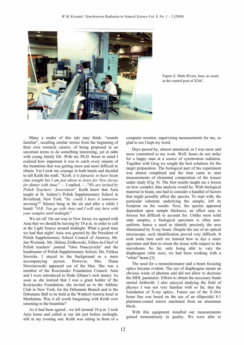
Experiment control post of X26C (Fig. 7) was located next to the hutch, along the beam direction. Mark Rivers (Fig. 8) was responsible for all its software. This included remote manipulation of the instrument components, such as step motors, data acquisition and analysis. The system relied on VAX computers, and data analysis programs were written in IDL (Interface Description Language). DECnet made it possible for Mark to carry out remotely a vast part of software development work.
Engaged in fascinating work as it was, I saw the days go by very fast. One Saturday Ania and I were leaving for a dinner party in Passaic, New Jersey. My key just
grated in the door lock when the phone rang. We were pretty short of time and I did not feel like opening the door but phone kept ringing insistently. A few more steps towards the car, and the ringtone seemed even louder. And what if something important happened? — I thought and returned home. It was Keith calling. Angry as hell at Keith I suspected bad news. Why on earth would he call Saturday afternoon? Sure it was not an invitation for dinner as at that time we still were not as close friends as we are now. My intuition did not fail me. "Hi Wjiech, I have a good news for you. In two hours you will have beam time at X26C. I presume you are happy to come" — I heard.
Figure 6. Setup for atomic physics experiments. Mark Rivers sitting at the back of the photo.
Figure 7. George Schidlovsky (left) and me at the measurements of lead concentration in bone tissue.
W.M. Kwiatek / Synchrotron Radiation in Natural Science Vol. 8, No. 1 – 2 (2009)
12
Figure 8. Mark Rivers, busy as usual, at the control post of X26C.
Many a reader of this tale may think: “sounds familiar”, recalling similar stories from the beginning of their own research careers, of being proposed in no uncertain terms to do something interesting, yet at odds with young family life. With my Ph.D. thesis in mind I realized how important it was to catch every minute of the beamtime that was getting more and more difficult to obtain. Yet I took my courage in both hands and decided to tell Keith the truth. "Keith, it is fantastic to have beam time tonight but I am just about to leave for New Jersey for dinner with Ania." — I replied. — "We are invited by Polish Teachers’ Association". Keith knew that Ania taught at St. Isidore’s Polish Supplementary School in Riverhead, New York. "So, could I have it tomorrow morning?" Silence hung in the air and after a while I heard: "O.K. You go with Ania and I will stay here with your samples until midnight."
We set off. On our way to New Jersey we agreed with Ania that we should be leaving by 10 p.m. in order to call at the Light Source around midnight. What a good time we had that night! Ania was greeted by the President of Polish Supplementary School Council of America, Mr. Jan Woźniak, Ms. Helena Ziółkowski, Editor-in-Chief of Polish teachers’ journal "Głos Nauczyciela" and the headmaster of Polish Supplementary School, Ms. Feliksa Sawicka. I stayed in the background as a mere accompanying person. However, Mrs. Diana Niewiarowski appeared out of the blue. She was a member of the Kosciuszko Foundation Council. Ania and I were introduced to Dede (Diana’s nick name). As soon as she learned that I was a grant holder of the Kościuszko Foundation, she invited us to the Athletic Club in New York, for the Debutante Branch and to the Debutante Ball to be held at the Waldorf-Astoria hotel in Manhattan. Was it all worth bargaining with Keith over returning to the beamline?
As it had been agreed , we left around 10 p.m. I took Ania home and called at our lab just before midnight, still in my evening suit. Keith was sitting in front of a
computer monitor, supervising measurements for me, so glad to see I kept my word.
Days passed by, almost unnoticed, as I was more and more committed to my work. Well, hours do not strike for a happy man at a source of synchrotron radiation. Together with Greg we sought the best solutions for the target preparation. The biological part of his experiment was almost completed and the time came to start measurements of elemental composition of the tissues under study (Fig. 9). The first results taught me a lesson on how complex data analysis would be. With biological material in beam, one had to consider a handful of factors that might possibly affect the spectra. To start with, the particular substrate underlying the sample, left its footprint on the results. Next, the spectra appeared dependent upon sample thickness, an effect easy to foresee but difficult to account for. Unlike most solid state samples, a biological specimen is often non-uniform, hence a need to identify precisely the area illuminated by X-ray beam. Despite the use of an optical microscope, such identification proved very difficult. It took some time until we learned how to dye a sister specimen and then to orient the tissue with respect to the microbeam. So far, only being able to vary the diaphragms (slits size), we had been working with a "white" beam [3].
The need for a monochromator and a beam focusing optics became evident. The use of diaphragms meant an obvious waste of photons and did not allow to decrease the MDL parameter. Efforts to obtain the necessary funds started forthwith. I also enjoyed studying the field of physics I was not very familiar with so far, that the foundation of X-ray optics.. Future use of the X-26A beam line was based on the use of an ellipsoidal 8:1 platinum-coated mirror machined from an aluminum block.
With this equipment installed our measurements gained tremendously in quality. We were able to

W.M. Kwiatek / Synchrotron Radiation in Natural Science Vol. 8, No. 1 – 2 (2009)
13
determine even small concentrations of elements we were interested in [4]. With the use of visualisation software that Mark wrote, spatial distributions of concentrations under study could be easily seen (Fig. 10). I looked at my work with satisfaction: not only was it extremely interesting but also had practical applications.
In the meantime Per Spanne was setting up tomography experiments. He placed a sample on the path of an intense, well collimated beam, an intensity monitoring detector right behind the sample (Fig. 11). The intensity of the incoming X-rays was measured by means of an ionisation chamber. In this way absorption of radiation by the sample could be determined accurately. The sample orientation with respect to the beam could then be varied and, by measuring the absorption coefficient as a function of sample orientation, a cross section of the inner structure of the sample could be reconstructed.
Per did this measurements in one plane but already it was apparent that the imaging capabilities of synchrotron beams would reach far beyond that achievement. Nowadays high resolution 3-D X-ray imaging is a routine measurement. Per illustrated his experiments by reconstructing a cross section of a pencil (Fig. 12).
Figure 9. Sample of rat cerebellum tissue we analysed.
Figure 10. Iron distribution in a selected area of tissue section shown in Fig. 9. The brighter the pixel the higher Fe concentration.
Figure 11. One of the first experimental set-ups for X-ray tomography.
Figure 12. Tomography image of a cross section of an office pencil.
One day in January 1987 I was busy doing measurements. Suddenly an announcement was broadcast: following a decision of the Lab Director, the working day would end at noon, due to an approaching snowstorm. Were they joking? — I thought. Only a few moments ago I walked from our building 901A to NSLS in full sunlight, under clear skies, without a trace of snow anywhere. Suddenly Al turned up. I hardly recognised him. He wore a hat covered with a thick layer of snow. I looked at him, amazed by the accuracy of the weather forecast. That very day Ania visited our friends at their place near the end of the Island. I rang them up only to learn that she had left an hour earlier. I was worried in earnest: how was she going to make it through such a blizzard, a driving license holder for half a year only. Another two hours of waiting and I could tell her at the doorstep how proud I was of her. There were many vehicles abandoned on L.I.E., with only one lane open for traffic. A couple of days later, with that snowstorm and my wife’s courage still in mind, I was again busy measuring on a Light Source. Suddenly the telephone rang. I answered with usual: "X26. Wojtek is speaking". The voice on the other side said: "Good morning Mr. Kwiatek. This is Dr. Halfen. I’m so glad to tell you: your
W.M. Kwiatek / Synchrotron Radiation in Natural Science Vol. 8, No. 1 – 2 (2009)
14
wife is pregnant". I was speechless for a good while with
teardrops of happiness around my eyes. Dr. Abraham
Halfen was Ania’s gynaecologist. Everything had
changed since then. We were awaiting the joy of our life.
Neither of us wanted to know the baby’s gender in
advance, although we were offered such information a
couple of times during medical examination. There was
something of a miraculous mystery in this uncertainty.
On September 22, 1987 our daughter Joanna (Joasia) was
born. Today she is a student at Jagiellonian University,
exploring the mysteries of biophysics. She already took
part in a few experiments on synchrotron beams in
Frascati and Hamburg. It looks like Dr. Halfen’s phone
call came at right time in a right place. I am very proud
of Joasia and sure Ania would also be… Or, rather,
she IS.
Until the end of my stay at Brookhaven I was
occupied not only with newborn Joasia but also with
collecting results for the Ph.D. thesis. The days, one by
one, were "growing tense" with more and more new
ideas, measurements, possible interpretations. Together
with my Ph.D. supervisor, professor A.Z. Hrynkiewicz,
we agreed as to the main contents of the thesis. It would
discuss optimum experimental conditions for
experiments on the elemental composition of biological
tissues. The thesis entitled "Trace element analysis using
synchrotron radiation" was completed in English, while
still at BNL. I am deeply thankful to Al Hanson, with
whom we made friends, for the revision of this work.
My stay at the BNL was originally planned for one
year. I owe it to Dr. Keith W. Jones, who believed in me
and who recognized my capabilities, that I spent there
three most fascinating years of my life.
All three of us returned to Poland on November 27,
1987 with my Ph.D. thesis ready to submit. The
adventure that began with an innocent group meeting at
the BNL lasts until now. The adventure with synchrotron
radiation.
Acknowledgements: Financial support from the Kosciuszko
Foundation for the Scholarship of 1984–1985 is highly
appreciated as well as funding through the US Department of
Energy and National Institutes of Healt grants during the the
extension of my stay at the BNL (1985–1987).
References
[1] J.G. Pounds, G.J. Long, W.M. Kwiatek, K.R. Reuhl, A.L.
Hanson, B.M. Gordon, K.W. Jones, "Application of
synchrotron radiation-induced x-ray fluorescence to trace
element toxicology", Toxicologist 6, 1 (1986) 208.
[2] A.L. Hanson, W.M. Kwiatek, K.W. Jones, "The use of a
SiTek position sensitive detector for synchrotron radiation
beam monitoring and alignment", Nucl. Instrum. Meth.
Phys. Res. A 260 (1987) 529-533.
[3] A.L. Hanson, K.W. Jones, B.M. Gordon, J.G. Pounds,
W.M. Kwiatek, G.J. Long, M.L. Rivers, S.R. Sutton, "Trace
element measurements using white synchrotron radiation",
Nucl. Instrum Meth. Phys. Res. B 24/25 (1987) 400-404.
[4] W.M. Kwiatek, G.L. Long, K.R. Reuhl, A.L. Hanson, K.W.
Jones, J.G. Pounds, "Distribution of Fe, Cu, Zn, and Hg in
the mouse cerebellum", Toxicologist 7, 1 (1987) 302a.
M. Stankiewicz / Synchrotron Radiation in Natural Science Vol. 8, No. 1 – 2 (2009
MY FIRST ENCOUNTER WITH SYNCHROTRON. 34 YEARS AGO
Marek Stankiewicz
Institute of Physics, Jagiellonian University, ul. Reymonta 4, 30-059 Kraków, Poland
Keywords: synchrotron, vacuum, ionization, coincidence
Synchrotron radiation?
It was already 34 years ago when I got aware of itsexistence for the first time!
It was the beginning of 1985. In my pigeon hole, atthe Jagiellonian University Institute of Physics there wasa letter from my good colleague, Leszek Frasiński, aformer assistant in the Department of Atomic Optics inthe Institute. Then, he had been working for the last fewyears for the Atomic and Molecular Spectroscopy Groupat University of Reading (UK). In the letter he verystrongly persuaded me to apply for a post doc position inReading. It was all about participating in a veryinteresting, in his opinion, research project regardingmolecular spectroscopy using synchrotron radiation. Thehead of the group was Prof. Keith Codling, which hadpioneered synchrotron radiation based research, fullyappreciating its research potential from the verybeginning [1]
I must admit that those days my knowledge of thesubject was none. Synchrotron radiation? Synchrotronmeans accelerator. What it has got to do with molecularspectroscopy was boggling my mind. Is it aboutcollisions? Electron- molecule? For sure this can not bethe case!
Nowadays, the first reaction would be to typesynchrotron radiation into a web search engine. Oneimmediately gets hundred thousands hits! However, thattime, hard to believe, there was no internet! It was up tomany hours in library, browsing through abstracts. Therewas not so many of them though. This was followed bytelephone calls to Reading (via operator, after manyhours of waiting) and conversations with Leszek. Somerequested literature arrived by mail (not email!). Afterfew weeks came the decision time.
I decided to go for it. I was convinced: this must be avery exciting project full of many challenges in diversefields. Already advanced talks with University of Stirlingabout a post doc position connected with someconventional high resolution optical spectroscopy had tobe abandoned.
Going abroad those days meant loads of formalities,young readers are not aware of. It had to start, of coursewith the passport application, submitting all variety offorms in Jagiellonian University SB (Secret Police)office. Will they accept the application or will they not?
After few weeks of apprehensive waiting – yes,passport was ready for collection! Now time for a trip toWarsaw to visit UK embassy and for an interview with aUK immigration officer in order apply for visa (hopefully
a multi-entry one) and work permit. After queuing longhours from early dawn eventually came a ratherunpleasant and comprehensive grilling. Questions aboutmembership to any political parties or organization,financial status, properties, personal situation, children,parents etc. Rather revolting experience, not far awayfrom interrogations by Polish SB. Apparently nothingsuspicious emerged and I was judged as an individualwho was not threatening the security of the UnitedKingdom of Great Britain and Northern Ireland. Afterfew weeks I was able to collect all the required stampsand documents. Eventually, at the beginning ofSeptember 1985 I was ready for take off to commencemy duties at University in Reading. One more thing to do– go and buy from a bank 10 USD with a special, verygenerous exchange rate—a special allowance for Polishcitizens going abroad those days!
On the 1st of October 1985 I took a seat on a PolishAirlines LOT flight from Kraków to Heathrow. Fromthere I took a bus to Reading, only 60 km (40 miles Ishould rather say!) west from Heathrow. There I was,looking forward to the new chapter in my career. Nextday, a morning meeting was planned at J.J. Thomson(1906 Nobel Prize in Physics for discovery of electron)Physical Laboratory. All members of the Atomic andMolecular Spectroscopy Group were present: KeithCodling, Leszek Frasiński, Kevin Randall and PaulHatherly.
The title of our project was: “Coincidence studies ofmolecular ions fragmentation using synchrotronradiation”. A sharp start was needed, timing was verytight. In the first four months we had to design andconstruct the devoted experimental setup (entireexperimental station) and design from scratch a dataacquisition system together with developing the relevantsoftware. We needed to divide the work. I was eager tobe in charge of the latter task. Electronics had beenalways my hobby and in the eighties PC computersjoined the game. Leszek, Kevin and Paul took on thedesign and construction of the experimental setup:vacuum chamber, time of flight analyzers, micro channeldetectors. This was definitely a big challenge time – forall of us. Many aspects of the tasks were new areas for allof us, including Keith.
Accordingly with the assignment, next day Iunpacked a brand new IBM AT PC computer with EGA(Enhanced Graphics Adapter—16 colours, 640×350pixels) graphics card and corresponding colour monitor. Iremember its serial number: 0011. Other parameters ofthe machine: CPU clock: 8 MHz, hard dick capacity:
15
M. Stankiewicz / Synchrotron Radiation in Natural Science Vol. 8, No. 1 – 2 (2009
20 MB, RAM memory: 624 kB. For the first time in mylife I switched on a PC. Armoured with a Fortrancompiler and Basic interpreter.
It was a thrill indeed! Those days, in Poland, the ITtechnology was represented mostly in the shape of SirSinclair’s ZX Spectrums (8 bit processor, few kB ofRAM). Sporadically one was able to see a Neptun –Polish clone of Commodore PET (another 8 bitmachine). These small machines, developed for theconsumer market were used in Polish researchenvironment for computational purposes and also somerelatively efficient data acquisition systems weredesigned utilising these ‘machines’, painfully interfacingthem with hardware. IBM PC XTs in ‘advanced’configuration with 10 MB hard disk equipped with DOSor CP/M operating system were just coming to Polandand were subjects of great admiration.
My AT was supposed to be the heart of the dataacquisition system of our experiment. The task was tocommunicate with a CAMAC crate equipped withAutonomous Logic and Arithmetic Unit, memory, a timeto digital converter and numerous auxiliary andinterfacing modules.
The goal was to have the acquired coincidencesdisplayed in real time as a false colour map. The first bigproblem came rather fast: tests revealed that it tookminutes to display such a 256×256 map (65536individual pixels) using the purchased Fortran graphicslibrary. For me that meant programming the graphicscard in assembler, if I was lucky. If not it meant using themachine code. Which was going to be the case anyway tocommunicate with the CAMAC controller. Some goodfun was ahead! The colleagues could not complain aboutlack of work either. The experimental setup was quitecomplicated, equipped wit rotatable double time-of-flight analyzers. Everything needed to be built fromscratch and experience was needed in designing thedetector setups and high vacuum hardware andinstrumentation. Our technician was also giving all hisbest to manage to machine all the bits and pieces in time.
Those days, in Kraków vacuum chambers were builtmostly of glass. This meant outgassing the Apiezongreased glass valves and continuous fight with smallleaks. Diffusion pumps were used with all the associatedproblems (presence of hydrocarbons, oil burning etc.).Vacuum conditioning lasted for days and weeks. Theglass blowing technician was the person to be in verygood relation with!
There we had to produce a high vacuum chamber,free of hydrocarbons to be able to connect it to thesynchrotron source termination. Forget glass, Apiezon,diffusion pumps etc. New vacuum culture had to beapplied: stainless steel chamber and fittings, turbomolecular pumps, KF and CF fittings and flanges.10-7
torr vacuum achievable in few hours. All newtechnology - quite a step forward.
That autumn and even the Christmas period was avery busy time for all of us; hard work. In January wewere almost ready. Came the last time for tests andmodifications. The acquisition system eventually seemed
to be working: collecting and displaying in real time thedata from a home built multi-coincidence simulatinggenerator. However, something was wrong: there werevery annoying intermittent problems. Thecommunication between the CAMAC controller and thePC sporadically got lost. This certainly was not good andmade me frustrated. However, as sometimes happens,after few days of furious tests the problem got resolvedby sheer accident. It was just a 5 m long, multi wireribbon cable connecting the PC with CAMAC, whichwas causing problems. But it was not as trivial as itscontacts. It was just when it was nicely arranged in a tidyroll when apparently some crosstalk between the signalswas scrambling the communication. An interesting lessonof applied electronics: keep the cables untidy!
Vacuum chamber was also ready, the two time offlight analyzers and the detectors tested. Ourexperimental session was planned in few weeks time atDaresbury Laboratory Synchrotron Radiation Source –the second generation UK synchrotron radiation facility– e.g. designed and built solely as a source ofsynchrotron radiation, mostly from bending magnets.
Eventually the time has come. We hired a van andafter filling it up with all the equipment we took off toDaresbury. Daresbury is a small village (few houses, achurch and of course a pub) in the north of England, nearManchester and Liverpool. On my way there I learnedthat it is known not only because of the synchrotronfacility there but because the author of "Alice’sAdventures in Wonderland", Lewis Carroll was bornthere. However his true name was Charles LutwidgeDodgson and his principal job was lecturing mathematicsat Christ Church College in Oxford in the second half ofthe XIX century. Apparently the place was special andwe were going to a wonderland!
The team appeared to be relaxed, however theprospect of using such a unique source of radiation andworking in the large scale facility environment increasedmy adrenaline level for sure. Above all, I am a researcherand an experimentalist hence I bound to be excited!
We drove very carefully. Such a fragile load neededspecial care. We did not want the detectors to crack fromthe vibration. Or any connections got loose inside thevacuum chamber. Eventually we arrived to Daresbury inthe evening. It took us some hours to unload and wheelthe equipment to the beamline (no. 3.11 – Seyamonochromator). When we finished it was time to gostraight to bed in a small hostel for the users run byDaresbury Laboratory. Next day morning we werewelcomed with typical English breakfast with toasts,fried eggs, sausages and baked beans. It made a perfectintroduction into our first session at Daresbury. So it hasstarted. Next month we spent on conquering ourexperiment, getting known all the control subtleties ofour beamline and the monochromator, learning thestorage ring refilling procedures; working 20 hours perday. The synchrotron crew had also their share ofproblems and challenges to provide a stable operation ina single bunch mode, which was required for ourexperiment in order to ionize oxygen molecules by a
16

M. Stankiewicz / Synchrotron Radiation in Natural Science Vol. 8, No. 1 – 2 (2009
17
everything one day everything was ready, the equipment
was fine tuned, stable single bunch stored in the ring –
and we started the real measurement! We were acquiring
coincidences between photons, electrons and ions! We
were watching, point after point, how our dreamt of
colour map of coincidences between the exciting light
pulse, photoelectron and photoion in the time of flight
(momentum) domain was built up in real time.
Everything was going as we planned – emerging map
illustrated energy levels in molecular oxygen – in colour
(Fig.1)! A wonderland indeed!
Figure 1. Electron-ion coincidences in ionization of O2
at 486 Å (25.5 eV). Coincidence features: B, predissociation of the B 2Σg
- state to O+(4S0) + O(3P); c,
v = 0 and v = 1, predissociation of the c 4Σu- state to the
limits O+(4S0) + O(3P) and O+(4S0) + O(1D); 1, repulsive state to the limit O+(4S0) + O(3P); 2, repulsive state III 2Πu to the limit O+(2D0) + O(3P). The horizontal line is due to cross-talk; the vertical lines are due to false coincidences. Taken from Ref. [2].
Of course, that day we had to celebrate this success in
the nearby, very popular (ask any of the Daresbury
Laboratory users!) "Ring’o’Bells" pub with "a pint or
two" of a decent English ale.
This is how my adventure with synchrotron radiation
based research has started. Since then, for the last 34
years, my research activities have been focused closely
on investigation of molecular processes excited by
synchrotron radiation.
The Daresbury Synchrotron Radiation Source ceased
its operation last year. UK research community has now
a new, advanced third generation synchrotron source –
“Diamond” available.
Nowadays I commute from Kraków mostly to MAX-
lab in Lund and to Sincrotrone Elettra in Trieste, where I
have met a very friendly environment. Keith Codling has
retired. Leszek Frasiński holds professorship at Imperial
College in London, Paul Hatherly works for Open
University in Milton Keynes (England-
Buckinghamshire) and the last place where I localized
Kevin Randall was Advanced Light Source in Berkeley
(California, USA). We are all still around synchrotrons. I
am sure that we all remember the period of our first
project at Daresbury as a very special one.
From that time the spectrum of synchrotron radiation
users has immensely broadened. Nowadays physicists are
just one of many groups representing diverse fields of
research done at synchrotron radiation facilities.
Investigations are carried out, amongst others, in such
fields as medicine, biology, chemistry, material science,
archaeology etc. Much has changed in the field of
electronics, IT technology, and vacuum generation.
There has been a big progress in synchrotron design and
associated instrumentation, focused on optimizing the
radiation output. There are many companies providing
synchrotron specific instrumentation which spun off
from relevant research projects. Many new synchrotron
radiation facilities have been built all around the world.
Availability of these unique sources of radiation allows
thousands of researchers from different fields for
performing experiments otherwise impossible. New,
fourth generation sources – Free Electron Lasers are the
latest challenge in the field. Some such facilities are
already operating (e.g. FLASH, TESLA in Europe)
another being constructed (FERMI), opening new
horizons in science.
I am writing these memories when there are strong initiatives to build in Poland a synchrotron radiation source and a free electron laser. I wish that one day in the nearest future at least one of these initiatives is going to be successful. I am convinced that this would be a great day. I am sure about the immense benefits which these projects could bring to the Polish research and education community.
Acknowledgements: I would like to thank Prof. Wojciech Paszkowicz for inviting me to write these memories. I mostly appreciate his initiative.
References: I have decided to refer only to two publications. Anyone interested in whichever aspect of synchrotron radiation is strongly encouraged to visit http://www.lightsources.org/cms/ where there is a copious amount of information available. [1] R.P. Madden, K. Codling,, “New autoionizing atomic
energy levels in He, Ne, and Ar”, Phys. Rev. Lett. 10, (1963) 516–518.
[2] J. Frasinski, M. Stankiewicz, K. Randall, P. Hatherly, K. Codling, "Dissociative photoionisation of molecules probed by triple coincidence; double time of flight techniques", J. Phys. B: Atom. Mol. Opt. Phys. 19 (1986) L819–L824..
Marek Stankiewicz
Instytut Fizyki UJ
Kraków, August 2009

VIII KSUPS 2009: Program / Synchrotron Radiation in Natural Science Vol. 8, No. 1 – 2 (2009)
8. Krajowe Sympozjum Użytkowników Promieniowania Synchrotronowego
Podlesice, 24-26 września 2009
KSUPS-8: 8th National Symposium of Synchrotron Users
organizowane przez
Instytut Fizyki im. Augusta Chełkowskiego, Uniwersytet Śląski w Katowicach,
Polskie Towarzystwo Promieniowania Synchrotronowego
KOMITET PROGRAMOWY
Krystyna Lawniczak-Jabłońska (IF PAN, Warszawa)Andrzej Burian (UŚ, Katowice)
Danuta Żymierska (IF PAN, Warszawa)Wojciech Paszkowicz (IF PAN, Warszawa)
Anna Wolska (IF PAN, Warszawa)Edward A. Görlich (UJ, Kraków)
Bogdan Kowalski (IF PAN, Warszawa)Bronisław Orłowski (IF PAN, Warszawa)
Paweł Piszora (UAM, Poznań)
KOMITET ORGANIZACYJNY
Alicja Ratuszna, Uniwersytet Śląski w KatowicachAndrzej Burian, Uniwersytet Śląski w KatowicachJacek Szade, Uniwersytet Śląski w Katowicach
Andrzej Ślebarski, Uniwersytet Śląski w KatowicachAleksander Bródka, Uniwersytet Śląski w Katowicach
Katarzyna Grzybowska, Uniwersytet Śląski w KatowicachŁukasz Hawełek, Uniwersytet Śląski w Katowicach
SPONSORZY
19
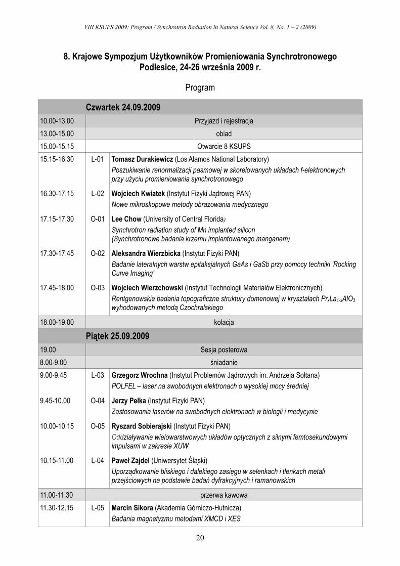
VIII KSUPS 2009: Program / Synchrotron Radiation in Natural Science Vol. 8, No. 1 – 2 (2009)
20
8. Krajowe Sympozjum Użytkowników Promieniowania Synchrotronowego Podlesice, 24-26 września 2009 r.
Program
Czwartek 24.09.2009
10.00-13.00 Przyjazd i rejestracja
13.00-15.00 obiad
15.00-15.15 Otwarcie 8 KSUPS
15.15-16.30 L-01 Tomasz Durakiewicz (Los Alamos National Laboratory)
Poszukiwanie renormalizacji pasmowej w skorelowanych układach f-elektronowych przy użyciu promieniowania synchrotronowego
16.30-17.15 L-02 Wojciech Kwiatek (Instytut Fizyki Jądrowej PAN)
Nowe mikroskopowe metody obrazowania medycznego
17.15-17.30 O-01 Lee Chow (University of Central Florida)
Synchrotron radiation study of Mn implanted silicon (Synchrotronowe badania krzemu implantowanego manganem)
17.30-17.45 O-02 Aleksandra Wierzbicka (Instytut Fizyki PAN)
Badanie lateralnych warstw epitaksjalnych GaAs i GaSb przy pomocy techniki 'Rocking Curve Imaging'
17.45-18.00 O-03 Wojciech Wierzchowski (Instytut Technologii Materiałów Elektronicznych)
Rentgenowskie badania topograficzne struktury domenowej w kryształach PrxLa1-xAlO3 wyhodowanych metodą Czochralskiego
18.00-19.00 kolacja
Piątek 25.09.2009
19.00 Sesja posterowa
8.00-9.00 śniadanie
9.00-9.45 L-03 Grzegorz Wrochna (Instytut Problemów Jądrowych im. Andrzeja Sołtana)
POLFEL – laser na swobodnych elektronach o wysokiej mocy średniej
9.45-10.00 O-04 Jerzy Pełka (Instytut Fizyki PAN)
Zastosowania laserów na swobodnych elektronach w biologii i medycynie
10.00-10.15 O-05 Ryszard Sobierajski (Instytut Fizyki PAN)
Oddziaływanie wielowarstwowych układów optycznych z silnymi femtosekundowymi impulsami w zakresie XUW
10.15-11.00 L-04 Paweł Zajdel (Uniwersytet Śląski)
Uporządkowanie bliskiego i dalekiego zasięgu w selenkach i tlenkach metali przejściowych na podstawie badań dyfrakcyjnych i ramanowskich
11.00-11.30 przerwa kawowa
11.30-12.15 L-05 Marcin Sikora (Akademia Górniczo-Hutnicza)
Badania magnetyzmu metodami XMCD i XES

VIII KSUPS 2009: Program / Synchrotron Radiation in Natural Science Vol. 8, No. 1 – 2 (2009)
21
12.15-13.00 L-06 Krystyna Ławniczak-Jabłońska (Instytut Fizyki PAN)
Charakteryzacja nanowytrąceń magnetycznych w matrycach na bazie GaSb
13.00-14.30 obiad
14.30-15.15 L-07 Maciej Kozak (Uniwersytet Adama Mickiewicza)
Wykorzystanie rozpraszania promieniowania synchrotronowego w badaniach błon biologicznych
15.15-16.00 L-08 Szymon Krzywda (Uniwersytet Adama Mickiewicza)
Struktura o atomowej rozdzielczości cytochromu c6 cyjanobakterii o niezwykłej sekwencji wtrąceń
16.00-16.15 O-06 Henryk Drozdowski (Uniwersytet Adama Mickiewicza)
Uporządkowanie krótkozasięgowe w orto-chloroanizolu w 293 K – rentgenowskie badania dyfrakcyjne
16.15-16.30 O-07 Krystyna Mazur (Instytut Technologii Materiałów Elektronicznych)
Rentgenowskie badania reflektometryczne chropowatości powierzchni kryształów podłożowych SiC i jej wpływu na stopień doskonałości strukturalnej osadzonych epitaksjalnych warstw SiC
16.30-16.45 przerwa kawowa
16.45-17.30 L-09 Radosław Przeniosło (Uniwersytet Warszawski)
Badania struktury tlenków metali przejściowych metodą dyfrakcji neutronów i promieni X
17.30-17.45 Wystąpienie przedstawiciela firmy PREVAC
17.45-18.00 Wystąpienie przedstawiciela firmy TESTCHEM
18.00-19.00 Zebranie PTPS
19.00 kolacja konferencyjna
Sobota 26.09.2009
8.00-9.00 śniadanie
9.00-9.30 L-10
Cen
trum
Pro
mie
niow
ania
Syn
chro
tron
oweg
o
Edward Goerlich (Uniwersytet Jagielloński)
Informacja na temat rozwiązań technicznych i stanu przygotowania do realizacji budowy synchrotronu w Polsce
9.30-9.50 L-11 Jacek Szade (Uniwersytet Śląski)
Pierwsza linia eksperymentalna na polskim synchrotronie: spektroskopie miękkiego promieniowania rentgenowskiego
10.00-13.00 (z przerwą kawową 11.00-11.30)
Plenarna (powszechna) dyskusja dotycząca aspektów merytorycznych I organizacyjnych proponowanych linii eksperymentalnych przy polskim synchrotronie [prowadzenie Edward A. Görlich i Krzysztof Tomala (Uniwersytet Jagielloński)]
13.00-14.00 obiad
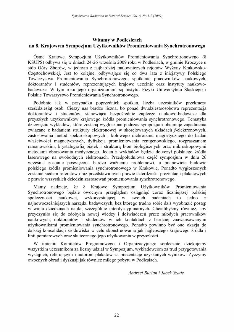
Synchrotron Radiation in Natural Science Vol. 8, No 1-2 (2009)
22
Witamy w Podlesicach
na 8. Krajowym Sympozjum Użytkowników Promieniowania Synchrotronowego
Ósme Krajowe Sympozjum Użytkowników Promieniowania Synchrotronowego (8 KSUPS) odbywa się w dniach 24-26 września 2009 roku w Podlesiach, w gminie Kroczyce u stóp Góry Zborów, w jednym z najbardziej malowniczych rejonów Wyżyny Krakowsko-Częstochowskiej. Jest to kolejne, odbywające się co dwa lata z inicjatywy Polskiego Towarzystwa Promieniowania Synchrotronowego, spotkanie pracowników naukowych, doktorantów i studentów, reprezentujących krajowe uczelnie oraz instytuty naukowo-badawcze. W tym roku jego organizatorami są Instytut Fizyki Uniwersytetu Śląskiego i Polskie Towarzystwo Promieniowania Synchrotronowego.
Podobnie jak w przypadku poprzednich spotkań, liczba uczestników przekracza sześćdziesiąt osób. Cieszy nas bardzo liczna, bo ponad dwudziestoosobowa reprezentacja doktorantów i studentów, stanowiąca bezpośrednie zaplecze naukowo-badawcze dla przyszłych użytkowników krajowego źródła promieniowania synchrotronowego. Tematyka dziewięciu wykładów, które zostaną wygłoszone podczas sympozjum obejmuje zagadnienia związane z badaniem struktury elektronowej w skorelowanych układach f-elektronowych, zastosowania metod spektroskopowych i kołowego dichroizmu magnetycznego do badań właściwości magnetycznych, dyfrakcją promieniowania rentgenowskiego, rozpraszaniem ramanowskim, krystalografią białek i strukturą błon biologicznych oraz mikroskopowymi metodami obrazowania medycznego. Jeden z wykładów będzie dotyczył polskiego źródła laserowego na swobodnych elektronach. Przedpołudniowa część sympozjum w dniu 26 września zostanie poświęcona bardzo ważnemu problemowi, a mianowicie budowie polskiego źródła promieniowania synchrotronowego w Krakowie. Ponadto wygłoszonych zostanie siedem referatów oraz przedstawionych prawie czterdzieści prezentacji plakatowych z prawie wszystkich dziedzin zastosowań promieniowania synchrotronowego.
Mamy nadzieję, że 8 Krajowe Sympozjum Użytkowników Promieniowania Synchrotronowego będzie owocnym przeglądem osiągnięć coraz liczniejszej polskiej społeczności naukowej, wykorzystującej w swoich badaniach to jedno z najnowocześniejszych narzędzi badawczych, bez którego trudno sobie dziś wyobrazić postęp w wielu dziedzinach nauki, szczególnie interdyscyplinarnych. Chcielibyśmy również, aby przyczyniło się do zdobycia nowej wiedzy i doświadczeń przez młodych pracowników naukowych, doktorantów i studentów w ich kontaktach z bardziej zaawansowanymi użytkownikami promieniowania synchrotronowego. Ponadto powinno być ono okazją do dalszej konsolidacji środowiska w celu skonstruowania jak najlepszego krajowego źródła i linii pomiarowych oraz skutecznego jego użytkowania w przyszłości.
W imieniu Komitetów Programowego i Organizacyjnego serdecznie dziękujemy wszystkim uczestnikom za liczny udział w Sympozjum, wykładowcom za trud przygotowania wystąpień, referującym i autorom plakatów za prezentację uzyskanych wyników. Życzymy owocnych obrad i dyskusji jak również miłego pobytu w Podlesiach.
Andrzej Burian i Jacek Szade

VIII KSUPS 2009: Abstracts / Synchrotron Radiation in Natural Science Vol. 8, No. 1 – 2 (2009)
SYNCHROTRON QUEST FOR BAND RENORMALIZATION
IN CORRELATED F-ELECTRON SYSTEMS
T. Durakiewicz 1
1 Los Alamos National Laboratory, MPA-10 Group, Los Alamos, NM87545, USA
Keywords: correlated electrons, 4f, 5f, photoemission
e-mail: [email protected]
Numerous low energy scales are observed in heavy
fermion materials. Information about some of the scales
is imprinted in the electron self-energy which can be
measured by angle-resolved photoemission (ARPES).
The successful line of attack in d-electron materials over
the last decade was based on using high energy- and
momentum-resolution photoemission techniques to
extract the self energy information from measured
spectra and applying many-body theoretical approaches
to find a link between self-energy and interactions:
electron-electron correlations, coupling to bosons,
magnetic fluctuations.
In 2008, we discovered a small energy scale in USb2,
via the observation of a kink in f-electron dispersion [1,
2]. The kink structure was observed for the first time in
any f-electron system. The kink energy scale of 21 meV
and the ultra-small intrinsic peak width of 3 meV were
seen. Our finding extended the context of quasiparticle
band renormalization from d to f-electrons, hence
creating a link between high temperature
superconductors and heavy fermions and actinide based
compounds. A new model of point-like Fermi surface
renormalization was proposed to explain the
spectroscopic properties of the kink.
In late 2008 we have found numerous kinks in the
band crossing the Fermi level along the G-M direction in
CeIrIn5. We have clearly identified two energy scales,
one leading to a kink at around 270 meV below Fermi
level that is related to the lower, incoherent part of the 4f
5/2 spin-orbit split, and another one at 7 meV below
Fermi level. The 7 meV renormalization may be related
to a maximum in phonon density of states observed by
inelastic neutron scattering experiments. The spin-
fluctuation energy scale of the order of 1 meV expected
to exist in this material is difficult if not impossible to
find with ARPES, due to the fundamental resolution
limitations. The third scale appears to be located around
20-25 meV above the Fermi level, and corresponds very
well to the size of hybridization gap predicted by
DMFT [3].
Our preliminary results look very promising, and we
plan to (i) expand the suite of f-electron materials where
kink structures can be characterized and (ii) link the
temperature evolution of self-energy with onset of
coherence in f-electron materials.
References
[1] T. Durakiewicz, P.S. Riseborough, C.G. Olson, J.J. Joyce,
P.M. Oppeneer, S. Elgazzar, E.D. Bauer, J.L. Sarrao, E.
Guziewicz, D.P. Moore, M.T. Butterfield, K.S. Graham,
"Observation of a kink in the dispersion of f-electrons",
Europhys. Lett. 84 (2008) 37003.
[2] X. Yang, P.S. Riseborough, T. Durakiewicz, C.G. Olson, J.J.
Joyce, E.D. Bauer, J.L. Sarrao, D.P. Moore, K.S. Graham,
S. Elgazzar, P.M. Oppeneer, E. Guziewicz, M.T. Butterfield,
"Unusual quasiparticle renormalizations from angle
resolved photoemission on USb2", Philos. Mag. 89 (2009)
1893–1911.
[3] J.H. Shim, K. Haule, G. Kotliar, "Modeling the localized-to-
itinerant electronic transition in the heavy fermion system
CeIrIn5" Science 318 (2007) 1615-1617.
23
L01

VIII KSUPS 2009: Abstracts / Synchrotron Radiation in Natural Science Vol. 8, No. 1 – 2 (2009)
24
NOVEL MICROSCOPY METHODS OF MEDICAL IMAGING
W.M. Kwiatek 1*, M. Podgórczyk 1, C. Paluszkiewicz 2, M. Gajda 3, Z. Stachura 1, M. Lekka 1, J. Lekki 1, M. Piccinini 4, and D. Grolimund 5
1 Institute of Nuclear Physics PAN, ul.Radzikowskiego 152, 31-342 Kraków, Poland
2 AGH University of Science and Technology, Al. Mickiewicza 30, 30-059 Kraków, Poland 3 Chair of Histology Collegium Medicum, Jagiellonian University, ul. Kopernika 7, 30-059 Kraków, Poland
4 INFN - Laboratori Nazionali di Frascati, Via E. Fermi 40, I-00044 Frascati, Italy 5 Swiss Light Source, Paul Scherrer Institut, 5232 Villingen PSI, Switzerland
Keywords: synchrotron radiation, medical imaging, SR-XRF, SR-FTIR, XANES
*) e-mail: [email protected]
Nowdays, the proper diagnosis requires medical imaging at scales ranging from single molecules through cells, tissues, organs, and up to whole body. Traditionally used optical microscopy and some other commonly used techniques quite often become insufficient for accurate diagnostics. Combining different imaging techniques may deliver complementary information from a sample, providing a combination of analytical performance that could enhance the accuracy of diagnosis and thus the quality of prognosis and possibly the speed of it.
Imaging technologies in different scientific areas have been rapidly developing in last decades, requiring higher and higher level of skills and knowledge. This puts medical specialists in a situation of continuous challenge to stay at the cutting edge of the technology already available to help patients timely and efficiently. Such a situation is obviously connected with synchrotron radiation based techniques.
SR-XRF (Synchrotron Radiation-X-ray Fluorescen-ce), XANES (Xray Absorption Near Edge Structure), SR-FTIR (Synchrotron Radiation – Fourier Transform InfraRed), micro-spectroscopy techniques as well as phase contrast microscopy, computer tomography, or a family of scanning probe microscopes (STM, NSOM, AFM…), give new opportunities of medical imaging.
Figure 1 presents the application of SR-XRF Zn distribution within tissue section [1] while Figure 2 shows an example of SR-FTIR image of the prostate cancerous tissue. A closer look at the results permitted to distinguish between the healthy, cancerous and hyperplastic parts of the tissue.
The examples of some other applications will be presented and discussed in terms of complementarities and opportunities. Acknowledgements: This work was supported by the European Community Research Infrastructure Action under the FP6 "Structuring the European Research Area" Programme,
contract No. RII-CT-2004-506008, project No. II-04-079EC and EU Integrated Infrastructure Initiative Hadron Physics Project, contract No. RII3-CT-2004-506078", Tari Programs No. 48, 67, and 85. Also, support from Ministry of Science and Higher Education is appreciated, Grant No. NN301464734.
(A) (B)
Figure 1. (A) Histological view of prostate tissue section, (B) Zn Distribution over the marked section, (C) High resolution 2D scan of Zn distribution over the “hot spot” [1].
Figure 2. Histological view of prostate cancerous tissue (left), 2D distribution of CH2/CH3 intensity ratio (right).
References [1] M. Podgórczyk, W.M. Kwiatek, D. Grolimund, C. Borca,
"Technical aspects of Zn microanalysis of human prostate cancer tissues and cells", Radiat. Phys. Chem. 78 (2009) S53-S57.
L02

VIII KSUPS 2009: Abstracts / Synchrotron Radiation in Natural Science Vol. 8, No. 1 – 2 (2009)
25
640 650 660
6540 6560 6580
Nor
mal
ized
Abs
orpt
ion
(arb
. uni
ts)
M nO
M n2O 3
M nO 2
M n foil
as grow n
300oC
500oC
700oC900oC
1000oC
M n L 3,2-edge
Photon Energy (eV)
M n foil M nO M n2O 3
M nO 2
M n K -edge
arb.
uni
ts
Photon Energy (eV)
SYNCHROTRON RADIATION STUDY OF Mn IMPLANTED SILICON
L. Chow 1*, A. Misiuk 2, C.W. Pao 3, D.C. Ling 3, W.F. Pong 3, and J. Bak-Misiuk 4
1 Dept. of Physics, University of Central Florida, Orlando, FL 32816 USA 2 Institute of Electron Technology, al. Lotnikow 46, 02-668 Warsaw, Poland
3 Dept. of Physics, Tamkang University, Tamsui, Taiwan, 25137, R.O.C. 4 Institute of Physics, PAS, al. Lotnikow 32/46, 02-668 Warsaw, Poland
Keywords: diluted magnetic semiconductor, spintronic materials, X-ray absorption spectroscopy
*) e-mail: [email protected]
Diluted magnetic semiconductors (DMSs) based on
III-V and II-VI compounds have been extensively studied for the last fifteen years [1]. However, for practical purpose, silicon-based DMS materials are much more desirable due to their compatibility with existing silicon technology. Recently, Bolduc et al. [2] reported room temperature ferromagnetism in Mn ion implanted silicon samples. This finding has generated a lot of new excitements in the DMS community.
Here we present the first synchrotron so called XMCD measurement on the MnSi system to clarify our understanding of the observed room temperature ferromagnetism in the Mn-implanted silicon. In addition, x-ray absorption spectroscopy of Mn L3,2 -edge, Mn K-edge, and magnetization measurements were also performed on the Mn-implanted silicon. Details of our findings are presented below.
Figure 1 displays the normalized Mn L3.2-edge XANES spectra [3] for the as-implanted and annealed samples. These spectra are compared with the Mn L3.2-edge XANES spectra of the reference Mn foil and of three different manganese oxides.
The normalized Mn L3,2-edge XANES and XMCD (denoted as I+ - I-) spectra for the as-implanted sample and the samples annealed at 300ºC, 700ºC, and 1000ºC
are presented in Figure 2. The general line shapes of I+ and I- are similar for the all samples. And it shows a barely vanishing XMCD intensity for the samples investigated, indicating that the average magnetic moment of Mn ions in silicon is almost zero.
Acknowledgements: DCL and WFP would like to thank the National Science Council of Taiwan for financial support under the grants Nos. NSC 96-2212-M-032-008-MY3 and NSC96-2212-M-032-012-MY3. LC would like to acknowledge a grant from US Agrecurtural Department.
References
[1] S.A. Wolf, D.D. Awschalom, R.A. Buhrman, J.M. Daughton, S. Von Molnar, M.L. Roukes, A.Y. Chtchelkanova, D.M. Treger, "Spintronics", Science 294 (2001) 1488.
[2] M. Bolduc, C. Awo-Affouda, A. Stollenwerk, M.B. Huang, F.G. Ramos, G. Agnello, V.P. LaBella, "Above room temperature ferromagnetism in Mn-ion implanted Si", Phys. Rev. B 71 (2005) 033302.
[3] A. Wolska, K. Lawniczak-Jablonska, S. Kret, P. Dluzewski, A. Szczepanska, M. Klepka, M.S. Walczak, Y. Lefrais, M.J. Hytch, A. Misiuk, "Atomic order in magnetic Mn inclusions in Si Crystals: XAS and TEM studies", J. Non-crystalline Solids 354 (2009) 418.
Figure 1 (left). XANES spectra of Mn-implanted silicon sample, as-implanted and annealed. For comparison, XANES spectra of manganese oxide and Mn metal are also shown. In the insert the Mn K X-ray absorption near edge spectra are shown. Figure 2 (right). Normalized Mn L3,2-edge XANES and XMCD spectra for as-implanted sample and samples annealed at 300ºC, 700ºC, and 1000ºC.
0
3
-0.6
0.0
0.61.2
1.8
0
3
-1.4
0.0
1.4
2.8
0
3
-0.6
0.0
0.6
1.2
1.8
630 640 650 660 670
0
3
-0.60.0
0.6
1.2
1.8
I+ I-
1000oC I+ - I-
300oC
700oC
Mn L3,2-edge
XM
CD
Inte
nsity
Nor
mal
ized
Abs
orpt
ion
(arb
. uni
ts)
as grown
Photon Energy (eV)
O 01

VIII KSUPS 2009: Extended Abstracts / Synchrotron Radiation in Natural Science Vol. 8, No. 1 – 2 (2009)
26
ROCKING CURVE IMAGING STUDIES OF LATERALLY OVERGROWN GaAs AND GaSb EPITAXIAL LAYERS
A. Wierzbicka 1*, D. Lübbert 2, J.Z. Domagała 1, and Z.R. Żytkiewicz 1
1 Institute of Physics, Polish Academy of Sciences, Al. Lotnikow 32/46, 02-668 Warszawa, Poland
2 Humboldt-Universität, Newtonstr. 15, 12489 Berlin, Germany
Keywords: III-V semiconductors, X-ray diffraction, digital synchrotron topography, epitaxial lateral overgrowth
*) e-mail: [email protected]
The development of modern electronics requires fast techniques that allow precise analysis of the structural quality of crystalline materials starting from bare wafers up to complicated semiconductor structures. The aim of this work was to apply synchrotron radiation based technique of Rocking Curve Imaging (RCI) for detection and visualization of crystalline lattice microdefects in laterally overgrown epitaxial (ELO) layers. Since ELO layers consist of parallel monocrystalline layers regularly arranged on a template (see Fig. 1) they are perfectly suitable to demonstrate the potential of the RCI technique.
Figure 1. Schematic drawing of ELO structure. L and w denote widths of the ELO wing and of the seeding line, respectively. Δα is the maximal tilt angle of the ELO lattice planes.
Briefly, RCI is a technique which combines the
features of X-ray imaging (very high spatial resolution) and X-ray diffractometry (very high angular resolution). The method is realized as follows (see Fig. 2): a wide, homogeneous and monochromatic synchrotron X-ray beam illuminates large parts of the sample. A precise goniometer allows rotating the sample close to the Bragg position with very small angular step around the axis perpendicular to the diffraction plane. Next, for each angular position series of local diffraction images are acquired by using very fast detector (Frelon camera - 2048×2048 pixels, pixel size equals to 1.4 µm). Finally, all digital images collected are used to create RCI maps of the sample that later on are visualized and analyzed with dedicated software [1].
Figure 2. Schematic drawing of RCI setup. A wide beam of monochromatic X-rays is diffracted on ELO sample. Diffraction plane is oriented horizontally, perpendicular to ELO stripes.
First we focus on the RCI analysis of a single GaAs ELO stripe grown by liquid phase epitaxy on SiO2-masked GaAs substrate. Details of the growth procedure can be found elsewhere [2]. Figure 3a shows the spatial distribution of Bragg peak position over a wide area of the sample. Signals coming from the substrate, from ELO wings and from the material grown vertically over the window in the mask are easily distinguishable.
Figure 3. Spatial distribution of Bragg peak position (a) and map of local rocking curve FWHM values (b) in GaAs/GaAs single ELO stripe. Pixel size is 1.4 µm.
substrate (GaAs or GaSb/GaAs) seed window
ELO layers SiO2 mask
Δα
w L
ELO stripes
incident synchrotron X-ray beam
rotation axis
ω
CCD camera
y
x
(a) (b)
FW
HM
(de
g)
O 02

VIII KSUPS 2009: Extended Abstracts / Synchrotron Radiation in Natural Science Vol. 8, No. 1 – 2 (2009)
27
Figure 3b shows the spatial distribution of the full width at half maximum (FWHM) of the rocking curve. As seen, FWHM is largest in the central part of the layer. Note that the Bragg angle position changes continuously across the ELO stripe. This is even better visible in Figure 4 that shows a cross-section at the position y = 539 of the map in Figure 3a. Such distribution of Bragg peak position clearly indicates tilting of ELO wings towards the mask – a phenomenon commonly observed in many ELO systems [2]. As can be seen, the maximum wing tilt angle, denoted as Δα in Figure 1, equals ~0.3°. Figure 4 shows that the fastest changes of the Bragg angle take place in the central part of the layer. Thus, the crystal lattice there must be strongly strained, which explains enhanced values of FWHM in that part of the layer (compare Figure 3b). Note also that RCI maps show that homoepitaxial GaAs/GaAs ELO layers are uniform along the ELO stripe. This is not necessarily the case in heteroepitaxial ELO layers where lattice and thermal expansion mismatches lead to strongly stressed epilayers.
Figure 4. x-omega-map of the GaAs/GaAs single ELO stripe.
As an example Figure 5 shows a map of local diffraction intensity in a GaSb ELO stripe grown on a GaAs substrate coated by a planar GaSb buffer and SiO2 mask. Local mosaicity in the wing area is clearly visible. Due to high spatial resolution of the RCI technique individual grains (microblocks) are visualized, so their sizes and relative misorientation can be readily determined.
Finally, results of RCI analysis of GaAs/GaAs and GaSb/GaAs ELO structures are compared with those obtained for the same samples by laboratory technique of spatially resolved X-ray diffraction (SRXRD) [3]. Due to
more intense synchrotron X-ray beam and application of modern detectors, the spatial resolution of RCI is much higher, which makes this technique preferable for the detection of strongly localized strain fields in textured heteroepitaxial structures. On the other hand, analyzer crystals can be easily used in laboratory SRXRD technique allowing precise separation of overlapping signals in homoepitaxial ELO layers [4, 5].
Figure 5. Spatial distribution of local diffraction intensity for GaSb/GaAs ELO layer. Pixel size is 1.4 µm. Microblock structure of the layer is visible.
Acknowledgements: This work was supported by special project ESRF/MA/623/2009 from the Polish Ministry of Science and High Education.
References
[1] D. Lübbert, T. Baumbach, "Visrock: a program for digital topography and X-ray microdiffraction imaging", J. Appl. Cryst. 40 (2007) 595–597.
[2] Z.R. Zytkiewicz, "Laterally overgrown structures as substrates for lattice mismatched epitaxy", Thin Solid Films 412 (2002) 64–75.
[3] J.Z. Domagala, A. Czyzak, Z.R. Zytkiewicz, "Imaging of strain in laterally overgrown GaAs layers by spatially resolved x-ray diffraction",Appl. Phys. Lett. 90 (2007) 241904.
[4] A. Czyzak, J.Z. Domagala, G. Maciejewski, Z.R. Zytkiewicz, "X-ray diffraction micro-imaging of strain in laterally overgrown GaAs layers. Part I: analysis of a single GaAs stripe ", Appl. Phys. A 91 (2008) 601–608.
[5] A. Czyzak, J.Z. Domagala, Z.R. Zytkiewicz, "X-ray diffraction micro-imaging of strain in laterally overgrown GaAs layers. Part II: analysis of multi-stripe and fully overgrown layers ", Appl. Phys. A 91 (2008) 609–614.

VIII KSUPS 2009: Abstracts / Synchrotron Radiation in Natural Science Vol. 8, No. 1 – 2 (2009)
28
X-RAY TOPOGRAPHIC INVESTIGATIONS OF DOMAIN STRUCTURE
IN CZOCHRALSKI GROWN PrxLa1-xAlO3 CRYSTALS
K. Wieteska 1, W. Wierzchowski
2*, A. Malinowska
2, S. Turczyński
2, M. Lefeld-Sosnowska
3,
D. Pawlak 2, T. Łukasiewicz
2, and W. Graeff
4
1 Institute of Atomic Energy POLATOM, 05-400 Otwock-Świerk, Poland
2 Institute of Electronic Materials Technology, ul. Wólczyńska 133, 01-919 Warsaw, Poland 3 Institute of Experimental Physics, University of Warsaw, ul. Hoża 69, 00-681 Warsaw, Poland
4 HASYLAB at DESY, Notkestr. 85, 22-603 Hamburg, Germany
Keywords: PrxLa1-xAlO3 crystals, domain structure, crystallographic defects, X-ray diffraction topography
*) e-mail: [email protected]
Praseodymium lanthanium aluminium perovskite is
interesting in view of the complicated phase transitions,
some of them ascribed to ion lattice coupling. One of the
aspects of the interest is connected with the preparation
of crystals with self-organized domain structure with
possible application in light guiding [1]. The open
problem in the technology of these crystals is the
characterization including examination of the regularity
and crystallographic features of the domain structure, and
the presence of common crystallographic defects, as
dislocations and inclusions.
In the present paper we attempted to apply the X-ray
diffraction topographic techniques exploring both
synchrotron and conventional X-ray sources to a number
of samples cut out from Czochralski-grown PrxLa1-xAlO3
crystals with different ratio of praseodymium and
lanthanum. The investigated crystals included both the
cases, when praseodymium replaced part of lanthanum
atoms, or was introduced as a dopant.
It is well known, that PrAlO3 similarly as LaAlO3 is a
rhombohedrally distorted perovskite (space group cR3 ,
tilt system aaa
rrr
) [2, 3]. The phase transition of PrAlO3
can be described as
C2/m ⎯⎯→⎯K150
Imma ⎯⎯→⎯K205
cR3 ⎯⎯ →⎯K1650
mPm3 .
The majority of the investigated samples contained
extended domain structure, expected to be a result of
twinning with {100} invariant twin planes. The domains
are visible using the optical microscopy equipped with
polarizers, or with Nomarski phase contrast, but some
fine details of the domains were previously studied with
the FM method [1]. The width of the particular domains
was in the range from tens to hundreds of micrometers.
The synchrotron X-ray topographic experiments were
performed using white synchrotron beam mainly in back
reflection geometry and only to some selected sample
the transmission X-ray topography was applied.
The conventional X-ray Lang topographs were taken for
a number of samples selected from parts of the crystals
with relatively low concentration of defects.
The synchrotron white beam topographs usually
reproduced the domains as series of mutually displaced
stripes corresponding to different orientation of
the crystal inside the domains. The density of domains
was different in the samples cut out from various crystals
with different composition, but generally it was most
numerous in the case of crystals with highest
concentration of praseodymium. In this case, the
synchrotron topographs usually revealed sets of domains
corresponding to more than one system of twinning. It is
also probable that in the case of most dense domain
structure the stripes revealed by the topographs
correspond rather to some sets of domains than single
domains. The representative topograph of a sample with
such a dense domain structure is shown in Fig. 1.
Figure 1. The representative white beam back-reflection
projection topograph of the sample cut out from
Pr0.75La0.25AlO3 crystal with extended domain structure.
The samples with low concentration of
praseodymium contained large single crystal regions,
where it was possible to reveal the individual
dislocations and the segregation fringes.
References
[1] D.A. Pawlak, T. Lukasiewicz, M. Carpenter, M.
Malinowski, R. Diduszko, J. Kisielewski, J. Cryst. Growth
282 (2005) 260.
[2] A.M. Glazer, Acta Crystallogr. B 28 (1972) 3384.
[3] A.M. Glazer, Acta Crystallogr. A 31 (1975) 765.
O 03

VIII KSUPS 2009: Abstracts / Synchrotron Radiation in Natural Science Vol. 8, No. 1 – 2 (2009)
POLFEL – THE HIGH AVERAGE POWER FREE ELECTRON LASER
G. Wrochna 1, J. Jasielski 1, J. Krzywiński 2, R. Nietubyć 1, J. Pełka 3, E. Pławski 1,J. Sekutowicz 4, R. Sobierajski 3, and J. Szewiński 1
1 The Andrzej Soltan Institute for Nuclear Studies PL-05500 Świerk, Poland2 SLAC National Accelerator Laboratory, 2575 Sand Hill Road, Menlo Park, CA94025, USA
3 Institute of Physics PAS, Al. Lotników 32/46, PL-00668 Warsaw, Poland4 Deutsches Elektronen-Synchrotron, Notkestrasse 85, D-22667 Hamburg, Germany
Keywords: free electron laser, linear accelerator, vacuum ultraviolet (VUV) source.
*) e-mail:[email protected]
A high average power VUV range free electron laserPOLFEL is planned at The Andrzej Soltan Institute forNuclear Studies in Świerk. The project is to satisfy thedemands for the intense coherent VUV light beamdeclared by numerous conventional laser laboratories aswell as synchrotron radiation users. We recognize it as animportant step in the growth of the experimentalcapabilities in natural sciences and material engineeringas well as a development of the FEL physics andtechnology.
The forthcoming paper will overview the generallayout of the planned facility, paying a special attentionto its novel solutions. The ground breaking feature ofPOLFEL is a continuous wave (cw) or near-cwoperation. It will be achieved with a linearsuperconducting (sc) accelerator fed with a lowemittance sc-electron injector furnished with the thin filmsc lead photocathode. In the article, we will present the
results of the electron beam dynamics start-to-endsimulation, a concept of variable polarization undulator,layouts of the diagnostics, timing and synchronizationsystems and general design of a two-fold branchedbeamline containing high energy resolution and highenergy density experimental stations.
We will describe a number of experimentsconstituting a preliminary approach to the scientificprogramme of the proposed FEL facility. The allpresented experimental techniques, base on the workbeing hitherto conducted in numerous laser andsynchrotron laboratories. They will extensively benefitfrom the new features brought by the proposed FELsource.
A brief overview of the POLFEL concept ispresented in the paper published in the currentissue.
29
L03

VIII KSUPS 2009: Abstracts / Synchrotron Radiation in Natural Science Vol. 8, No. 1 – 2 (2009)
APPLICATIONS OF FREE ELECTRON LASERS
IN BIOLOGY AND MEDICINE
J.B. Pełka 1*, G. Wrochna 2, R. Nietubyć 2, and K.R. Tybor 3
1 Institute of Physics, Polish Academy of Sciences, Warsaw, Poland2 The Andrzej Soltan Institute for Nuclear Studies, Świerk, Poland
3 Medical University of Łódź, Department of Neurosurgery, Łódź, Poland
Keywords: free electron laser, coherent diffraction imaging, ultrafast spectroscopy, radiation damage,
tissue ablation, ultrafast dynamics, laser surgery
*) e-mail: [email protected]
Synchrotron radiation (SR), both from storage ringsand from free electron lasers (FEL), has been extensivelyapplied in biology and in medicine for more than thirtyyears, opening up new opportunities to study life formson different levels, from biomolecules and subcellularstructures up to whole organisms [1, 2]. Intensesynchrotron beams turned out to be invaluable in softtissue probing with superior sensitivity, capable to detecteven small tissue variations.
In recent few years, a rapidly growing interest inapplication of FEL beams is observed in many areas ofscience and technology. It is due to the fact that FELsshow specific advantages to classical SR synchrotronsources, strongly enhancing probing of soft matterstructure and dynamics of processes with very highspatial and temporal resolution. They were alsosuccessfully tested as precise tissue ablation tools insurgery and oncology being superior to regularly usedclassical laser sources.
FELs utilize a relativistic electron beam as a lasingmedium. As a result, a monochromatic radiation isgenerated in ultrafast pulses, of duration down to the fsrange, with a unique combination of tunability,coherence, polarization, and high power that can exceedmore than 1 GW in a single pulse. Some FEL types candeliver radiation in the spectral regions of shortwavelengths, ranging from vacuum ultraviolet (VUV-FEL) to X-ray regions (X-FEL), unattainable with othertypes of lasers. Spectral brightness of the new X-FELsources, to be operational in the next few years, will beup to 9 orders of magnitude higher, as compared to themost intense 3GLS sources and will reach a value of 1029
photons/s · mrad2 · mm2 · 0.1% BW, emitted in ultrafastpulses of only 10-20 fs [3].
The aim of this report is to draw a spectrum ofbiomedical applications at FEL sources operating with awide ranges of wavelegths, from Terahertz up to soft X-
rays, that are currently available at various FELmachines. It will be shown, basing on examples ofparticular applications, the importance of the newsources to study ultrafast dynamics of life processes,imaging soft tissue and proteins with unprecedentedspatial resolution, as well as search of new medicaltechniques for surgery and therapy, which can be furthertransferred to common clinical tools with conventionalintense lasers. Possible biomedical applications at thePolish Free Electron Laser (POLFEL), proposed to bebuilt at the Andrzej Soltan Institute for Nuclear Studies inŚwierk near Warsaw will be metioned as well.
Acknowledgements: This work has been partially supported
by the Ministry of Science and Higher Education of Poland,
SPB nr. DESY/68/2007.
References
[1] G. Margaritondo, Y. Hwu, J.H. Je, "Synchrotron light in
medical and materials science radiology", Rivista del
Nuovo Cimento 27 (2004) 1–40.
[2] J.B. Pełka, Acta Phys. Polon. "Synchrotron radiation in
biology and medicine", 114 (2008) 309–330.
[3] N. Patel, "Shorter, brighter, better", Nature 415 (2002) 110–
111.
30
O 04

VIII KSUPS 2009: Abstracts / Synchrotron Radiation in Natural Science Vol. 8, No. 1 – 2 (2009)
INTERACTION OF MULTILAYER OPTICS WITH INTENSE FEMTOSECOND XUV PULSES
R. Sobierajski 1,2*, M. Jurek 1, D. Klinger1, A.R. Khorsand 2, E. Louis 2, S. Bruijn 2,R. van de Kruijs 2, E.D. van Hattum 2, K. Sokolowski-Tinten 3, U. Shymanovich 3, S. Toleikis 4,
H. Wabnitz 4, K. Tiedtke 4, N. Stojanovic 4, L. Juha 5, J. Chalupsky 5, J. Cihelka 5,V. Hajkova 5, E.M. Gullikson 6, and F. Bijkerk 2#
1 Institute of Physics Polish Academy of Sciences, Al. Lotników 32/46, PL 02-668 Warszawa, Poland2 FOM-Institute for Plasma Physics Rijnhuizen, Edisonbaan 14, NL-3430 BE Nieuwegein, The Netherlands,
3 Institut fuer Experimentelle Physik, Universitaet Duisburg-Essen, Lotharstr. 1, 47048 Duisburg, Germany4 HASYLAB/DESY, Notkestrasse 85, D-22603 Hamburg, Germany
5 Institute of Physics AS CR, Na Slovance 2, 182 21 Prague 8, Czech Republic6 Center for X-Ray Optics, Lawrence Berkeley National Laboratory Berkeley, CA 94720 USA
# also at MESA+ Institute for Nanotechnology, University of Twente, The Netherlands
Keywords: XUV, FEL, damage, multilayer optics
*) e-mail: [email protected]
Multilayer coated optics are used for control of XUVand soft X-ray radiation in many fields of science andtechnology, and has experienced a considerable boost oftechnology due to the application in advancedphotolithography. A new field is the application inexperiments at short wavelength Free Electron Lasers.This includes the x-ray sources – LCLS (USA), XFEL(Europe) & SPRING8 (Japan) and the XUV source –FLASH (Germany), ELETTRA (Italy). Multilayer coatedoptics are most promising candidates for optical schemesat such sources, fulfilling extreme requirements in termsof figure and roughness errors, wavefront preservation,and stability. It enables deflection angles much largerthan those reasonably achieved with monolayer mirrors.In addition, due to its good wavelength selectivity, it canbe used as a narrow band filter.
The photon flux from short wavelength Free ElectronLasers is extremely high. In the case of FLASH,operating in the XUV regime the ~10 fs long pulses canhave energy of up to 50 µJ, corresponding to 1011 W/cm2
for a 4 mm beam spot on the optics. This is at least 10orders of magnitude higher than in the case oflithography. Damage or even destruction of the opticscan be expected. Moreover, for some application themirrors have to be placed in the focused beam. In thiscase the intensity on the optics is even higher and canreach 1014 W/cm2. Under such conditions the opticalproperties of the reflecting elements would be changedalready during the pulse and the mirror would not work.These two effects, permanent damage of the coatings andchange of the optical properties of materials under highintensity XUV irradiation, can limit the performance ofthe multilayer optics.
We have carried out research on the flux resistivity ofa standard MoSi multilayer for a wavelength range in thesoft X-ray / XUV part of the spectrum by means ofexposures at FLASH. Samples were irradiated atdifferent intensity levels with single shots.
Morphological and structural surface changes weremeasured with phase-contrast microscopy, atomic forcemicroscopy and scanning transmission electronmicroscopy. The dynamics of damage were studied bymeans of time resolved microscopy. The damagemechanisms was determined as an ultrafast silicidesformation induced by enhanced diffusion in a melted Silayer.
The other operating regime where multilayers can beused is when the coating reflects only during the pulse(and is possibly damaged shortly after): the range ofsingle shot optics. However, under irradiation withultrashort intense pulses the mirror reflectivity candecrease even within the timeframe of the fs pulse due tothe change of the layers' optical properties – namely thereal and imaginary part of the refractive index. Theresponsible physical process is a strong electron gasexcitation during the pulse [1] which depends on thestructure of the multilayer and materials used. Thephenomenon was studied by means of angular resolvedreflectivity measurements at different intensities.
The results will be used as input for the furtherdevelopment of multilayer coatings for the shortwavelength FEL optics.
Acknowledgements: The authors wish to thank the staff ofFLASH at DESY, Hamburg, Germany for supplying the beamtime at FLASH. This work has been partially supported by theFoundation for Fundamental Research on Matter (Stichtingvoor Fundamenteel Onderzoek der Materie, FOM), theNederlandse Organisatie voor Wetenschappelijk Onderzoek(NWO) for funding this research and the Ministry of Scienceand Higher Education of Poland, SPB nr. DESY/68/2007.
References
[1] S. Hau-Riege et al., "Subnanometer-scale measurements ofthe interaction of ultrafast soft x-ray free-electron-laserpulses with matter", Phys. Rev. Lett. 98 (2007) 145502.
31
O 05

VIII KSUPS 2009: Abstracts / Synchrotron Radiation in Natural Science Vol. 8, No. 1 – 2 (2009)
32
LOCAL AND LONG RANGE ORDERS IN TRANSITION METAL OXIDES
AND SELENIDES AND METAL ORGANIC FRAMEWORKS STUDIED
USING COMBINED TECHNIQUES (XRD AND IN-SITU RAMAN)
P. Zajdel 1*
, I. Kruk 2,3
, P-Y. Hsieh 2,5
, W. van Beek 4, and M.A. Green
2,5
1 Institute of Physics, University of Silesia, ul. Uniwersytecka 4, 40-007 Katowice, Poland 2 NIST Center for Neutron Research, 100 Bureau Drive, Gaithersburg MD-20899, USA
3 Department of Chemistry, University College of London, 20 Gordon Str, WC1H 0AJ London, UK 4 Swiss-Norwegian Beamline, ESRF, Grenoble Cedex F-38043, France
5 Materials Science & Engineering, University of Maryland, College Park MD-20742-6033, USA
Keywords: transition metal, x-ray diffraction, Raman spectroscopy
*) e-mail: [email protected]
Constant development of synchrotron radiation
sources opens up new avenues in investigation of local
and long range structure of materials. On one side, it
improves already existing techniques like powder
diffraction (XRD) by increasing their angular and time
resolutions. On the other hand, the increased signal to
noise ratio allows to extract new useful information from
the same data, like the Pair Distribution Function (PDF)
encoded in the background of XRD.
Unfortunately, the long time needed for such „one-
shot” experiments makes them unusable for regular use.
The solution to this problem is the use of combined
techniques to obtain the equivalent information in a
shorter time, while maintaining the correlation between
the studied properties and the external stimulus like the
temperature or pressure.
While the XRD remains the method of choice for the
long range structure, the local properties can be obtained
using different techniques with Extended X-Ray
Absorption Fine Structure (EXAFS) being the prominent
example. However, when light elements (C, N, O, H) are
involved, Raman spectroscopy is more advantageous.
Figure 1. Evolution of Raman signal on heating up of
holmium based MOF. The dark strips mark point
where the first solvent molecule is lost. The sudden
increase of signal at dataset 60 is due to decomposition
of the compound.
The presentation will include results obtained for 3
classes of materials: seleno-spinels (ZnCr2Se4),
transition metal (TM) oxides and metal-organic
frameworks (MOF). In particular, MOFs recently fueled
rapid development of these combined techniques due to
their possible applications as a storage material for use in
the hydrogen based economy.
Research was conducted at the ESRF beamline BM1
(Swiss-Norwegian Beamline) [1] and consisted of
simultaneous measurements of XRD and Raman spectra
in the temperature range from 90 K to 700 K as well as
under the gas pressure up to 20 bar.
For the chalcogenides and oxides we have searched
for the signature of local deformations happening at
temperatures higher than the critical temperature of the
long range structural transition. In the case of oxides the
distortions were expected to appear due to Jahn-Teller
effect, for selenides due to possible magnetostriction.
For the metal-organic materials the research aimed at
finding the correlation between structural properties of
the host framework and the amount of the guest species
adsorbed inside it as function of the temperature and
pressure.
In the first part the as-synthesized MOF was heated
up in order to empty up the structure from the solvents
used during the synthesis (Fig. 1). Here, Raman
spectroscopy was used to monitor the disappearance of
the signal from guest molecule and host-guest
interactions. Such approach is much superior than the
usual two step, „off-line” technique, when material is
desolvated separately at high temperature, then
transferred to different place where the XRD study is
made at (usually) different temperature.
In the next step, while different gases were
introduced to the empty system, the Raman spectra was
used to monitor the interactions between host and the
adsorbed gas while XRD patterns are used to verify the
position of adsorption sites.
Additionally the time resolution of the order of
minutes allowed to identify new intermediate phases and
check the phase integrity upon cooling.
References
[1] E.Boccaleri et al., J. Appl. Crystallogr. 40. (2007) 684.
L04

VIII KSUPS 2009: Abstracts / Synchrotron Radiation in Natural Science Vol. 8, No. 1 – 2 (2009)
33
STUDY OF MAGNETISM WITH XMCD AND XES
M. Sikora *
Faculty of Physics and Applied Computer Science, AGH University of Science and Technology,
Av. Mickiewicza 30, 30-059 Kraków, Poland
Keywords: Magnetic moments, X-ray magnetic circular dichroism, X-ray emission spectroscopy
*) e-mail: [email protected]
X-ray absorption and emission spectroscopy techniques give an element and symmetry sensitive insight into the electronic structure of condensed matter. Using intensive hard X-rays produced by modern synchrotron sources bulk and surface properties of solid and liquid phases may be studied in-situ in a demanding sample environments, e.g. extreme temperatures, high pressure, high magnetic field, etc.
In this contribution the experimental and theoretical aspects of X-ray Magnetic Circular Dichroism (XMCD) and high resolution Kβ X-ray emission spectroscopy (XES) in the element selective investigation of magnetic moments will be presented and illustrated with examples of spotlight publications found in literature accompanied with a specific application example for each of the techniques to be discussed in details.
The first example will focus on the evolution of spin and orbital moment of rhenium in Ca2FeReO6 double perovskite upon application of strong magnetic field. Using an energy dispersive XMCD setup combined with a pulsed magnetic field installation, magnetic moment of Re was observed in a wide temperature (10-250 K) and magnetic field (up to 30 T) range, Fig. 1. The results reveal a spatial separation between two phases characterised by the different magnetostructural coupling and the distinct transport properties. A strong external magnetic field controls the relative abundance of the phases, thus having a strong influence on the average structural and electronic properties and being responsible for colossal magnetoresistance phenomena observed in this compound.
Figure 1. Low temperature, high field magnetisation dependence of the rhenium magnetic moment in Ca2FeReO6 double perovskite as derived from the Re L2,3-edge XMCD spectra acquired using pulsed magnetic field generation.
In the second example the application of X-ray emission and absorption spectroscopy to study the electronic and magnetic properties of LaMn1-xCoxO3 solid solution will be shown. Combined analysis of the K-edge absorption edges and Kβ emission lines is applied to determine the average charge and spin of the transition metal ions. Quantitative analysis of the spectral shape reveal electron transfer from Mn to Co site with a tendency to creation of Co2+/Mn4+ ordered phase. Comparison of the charge and spin evolution revealed that Mn3+/4+ and Co2+ ions are in their high spin configurations. The Co3+ ions are at room temperature in their low spin configuration up to x ≤ 0.6, while at higher doping level an increase of the average Co3+ spin state is observed, which plausibly explains the magnetization anomalies observed in the bulk magnetization measurements.
Figure 2. Comparison of the average Co charge and spin evolution in LaMn1-xCoxO3 perovskite series as derived from the K-edge energy shift (stars) and shape of the Kβ emission spectra (circles), respectively. Inset shows evolution of the average Co3+ spin state.
Acknowledgements: The authors are indebted to P. Glatzel, P. van der Linden, O. Mathon, S. Pascarelli, T.-C. Weng, Z. Jirak, K. Knizek, V. Prochazka, J.M. DeTeresa, R. Ibarra, J. Michalik, D. Zajac and Cz. Kapusta for support and valuable discussions. European Synchrotron Radiation Facility, Grenoble, is acknowledged for providing beamtime. This work was partly supported from the AGH UST project 11.11.220.01 "Basic and applied research in nuclear and solid state physics".
0.0 0.2 0.4 0.6 0.8 1.0
0.0 0.2 0.4 0.6 0.8 1.0
0.0
0.5
1.0
1.5 2+
Ave
rage
cha
rge
CHARGE SPIN
Ave
rage
spi
n
x (Co concentration)
Co
3+
Co3+
L05

VIII KSUPS 2009: Extended Abstracts / Synchrotron Radiation in Natural Science Vol. 8, No. 1 – 2 (2009)
34
CHARAKTERYZACJA NANO-WYDZIELEŃ
W MATRYCACH NA BAZIE GaSb
K. Lawniczak-Jablonska 1*
, A. Wolska 1
, M.T. Klepka 1, J. Sadowski
1,2,
A. Barcz 1
, A. Hallen 3
, and D. Arvanitis 4
1 Institute of Physics PAS, al. Lotników 32/46, 02-668 Warsaw, Poland
2 Lund University, MAX-Lab, Lund SE-221 00, Sweden 3 Royal Inst. of Technology, Dept. of Microelectronics and Applied Physics, Box 226, SE 164 40 Kista, Sweden
4 Department of Physics and Materials Science, Uppsala University, Box 530, 75121 Uppsala, Sweden
Słowa kluczowe: MnSb, GaSb, nano-inclusions, spintronics
*) e-mail: [email protected]
Heterostruktury składające się z metalicznych
ferromagnetycznych warstw nałożonych na materiał
półprzewodnikowy są potencjalnie użyteczne dla
zastosowań spintronicznych. Wśród nich te, wytworzone
przez wprowadzenie ferromagnetycznych wtrąceń do
matrycy półprzewodnikowej wydają się być bardzo
obiecujące. Wymaga to przygotowania systemu w taki
sposób, żeby małe ferromagnetyczne nanocząstki były
zanurzone w sieci materiału półprzewodnikowego. Taki
złożony materiał może być rozważany jako
półprzewodnik wypełniony nanomagnesami
dostarczającymi wbudowanego pola magnetycznego.
Przeprowadzono wiele badań wydzieleń MnAs w
matrycy GaAs, natomiast stosunkowo mało doniesień
literaturowych dotyczy badań wydzieleń MnSb. Materiał
ten wydaje się interesujący, ponieważ jego temperatura
Curie jest wyższa niż temperatura pokojowa, co otwiera
nowe możliwości jego wykorzystania.
Jako materiał referencyjny zbadano komercyjny
proszek MnSb oraz warstwy MnSb wyhodowane metodą
MBE na podłożach GaAs(111)B oraz GaAs(100).
Okazało się, że warstwy te są niejednorodne i wykazują
tendencje do wzrostu domenowego o kierunku zależnym
od struktury podłoża. Stwierdzono również ślady innych
faz. Topografia wzrostu tych warstw jest również różna
(Rys. 1), co jest zgodne z doniesieniami literaturowymi
[1-3]. Również materiał proszkowy wykazywał obecność
fazy MnSb o dużym stopniu zdefektowania. Wydaje się,
że materiał ten wykazuje naturalną tendencję do
segregacji powinien więc być dobrym kandydatem do
wytworzenia nano-wydzieleń pod warunkiem
opracowania odpowiedniej technologii.
Zostaną zaprezentowane wyniki prób wytworzenia
ferromagnetycznych nano-wydzieleń MnSb za pomocą
różnych technologii. Mn był wprowadzany do matrycy
GaSb zarówno w procesie MBE, jak i poprzez
implantację. Stosowano różne warunki wzrostu oraz
różne dawki i sposoby poimplantacyjnego wygrzewania.
Na tak przygotowanych próbkach przeprowadzono
pomiary absorpcji rentgenowskiej, pomiary rozkładu
pierwiastków w funkcji głębokości oraz pomiary
dyfrakcyjne, mikroskopowe i magnetyczne w celu pełnej
charakteryzacji utworzonych wydzieleń.
a)
b)
Rysunek 1. Obrazy AFM topografii powierzchni dla
probki a) MnSb na GaAS(111)B i b) dla MnSb na
GaAs(100).
Stwierdzono, że bardzo trudno jest wytworzyć
wydzielenia MnSb za pomocą implantacji, ponieważ Mn
znacznie łatwiej łączy się z tlenem niż antymonem.
Ponadto w procesie wygrzewania antymon łatwo ulatnia
się z próbki i w efekcie tworzą się wydzielenia GaxMny.
L06

VIII KSUPS 2009: Extended Abstracts / Synchrotron Radiation in Natural Science Vol. 8, No. 1 – 2 (2009)
35
6520 6540 6560 6580 6600 6620 6640
KMn
HT-2
HT-5
Abso
rpcja
(arb
.u.)
Energia (eV)
Rysunek 2. XANES na krawędzi K manganu.
0 1 2 3 4 5
HT-2
HT-5
|χ(R
)| (
Å-3
)
R (Å)
Rysunek 3. Transformata Fouriera oscylacji EXAFS na
krawędzi K manganu.
W przypadku wydzieleń hodowanych metodą MBE
stwierdzono silną zależność od temperatury wzrostu,
koncentracji Mn oraz od kierunku i rodzaju podłoża.
Struktury z wydzieleniami MnSb udało się wyhodować
jedynie na podłożach GaSb(100) oraz GaAs(111)B. Dla
obydwu podłoży w procesach prowadzonych w
temperaturze powyżej 450ºC znacząca część atomów
manganu lokowała się w sieci GaAs lub GaSb (próbka
HT-2, Rys. 2 i 3). Dopiero dla temperatury 450ºC udało
się wytworzyć wydzielenia MnSb o strukturze
heksagonalnej (próbka HT-5, Rys. 2). Zmiany w
sposobie wiązania atomów manganu są widoczne
zarówno w strukturze XANES (Rys. 2), jak i w
rozkładzie atomów wokół Mn uzyskanym z analizy
EXAFS (Rys. 3).
Zaobserwowano również zależność od koncentracji
Mn dla obydwu rodzajów podłoża. Wynika z niej, że w
próbkach o wyższej zawartości manganu wykształciła się
struktura MnSb. Natomiast tam, gdzie zawartość
manganu jest bliska 1% tylko część atomów lokuje się w
wytrąceniach MnSb, zaś reszta podstawia się w miejsce
antymonu w strukturze GaSb. Wielkość nano-wydzieleń
zależy od zawartości Mn oraz szybkości wzrostu
struktury, natomiast kierunek wzrostu i topologia
struktury zależą od rodzaju podłoża.
Absorpcja rentgenowska jako technika selektywna ze
względu na rodzaj pierwiastka okazała się idealnym
narzędziem do określenia sposobu wbudowania się
atomów Mn wprowadzanych do matrycy GaSb za
pomocą różnych technologii. Wykazano, że widma
absorpcyjne mogą być wskaźnikiem utworzenia się
wydzieleń w matrycach półprzewodnikowych.
Podziękowania: Autorzy wyrażają podziękowanie za
finansowanie uzyskane dzięki grantowi Ministerstwa Nauki i
Edukacji N202-052-32/1189 oraz DESY/HASYLAB i Unii
Europejskiej w ramach projektu RII3-CT-2004-506008 (IA-
SFS).
Literatura
[1] H. Akinaga, K. Tanaka, K. Ando, T. Katayama,
"Fabrication and magneto-optical properties of epitaxial
ferromagnetic Mn1-xSb thin films grown on GaAs and
sapphire", J. Cryst. Growth 150 (1995) 1144–1149.
[2] S.X. Liu, S.M. Bedair, N.A. El-Masry, "Mn-prelayer effects
on the epitaxial grouth of MnSb on (11) B GaAs by pulsed
laser deposition", Mat. Lett. 42 (2000) 121–129.
[3] A.F. Panchula, C. Kaiser, A. Kellock, S.S. Parkin, "Spin
polarization and magnetotransport of Mn–Sb alloys in
magnetic tunnel junctions", Appl. Phys. Lett. 83 (2003)
1812–1814.

VIII KSUPS 2009: Abstracts / Synchrotron Radiation in Natural Science Vol. 8, No. 1 – 2 (2009)
36
SMALL ANGLE SCATTERING OF SYNCHROTRON RADIATION
STUDIES OF BIOMEMBRANES
M. Kozak
Department of Macromolecular Physics, Faculty of Physics A. Mickiewicz University,
ul. Umultowska 85, 61-614 Poznań, Poland
Keywords: phospholipids, surfactants, small angle X-ray scattering
*) e-mail: [email protected]
Cell membranes consists of lipids, proteins and
carbohydrates. Phospholipids are the main group of cell
membranes lipids. The occurrence of a hydrophilic and a
hydrophobic part in the phospholipide molecule
determined their ability to self-organization in such
solvents as water. Fully hydrated phospholipids exhibit
tendency to aggregation and formation of different
structural phases. Typical for phospholipids lamellar
phases (lamellar gel phase, rippled phase, liquid
crystalline phase) are formed by stacks of bilayers and
water. The cubic phases are formed by spherical micelles
organized in cubic lattice or bicontinuous 3D-network of
finite phospholipids rods. The hexagonal phase is
composed of hexagonally packed long rods formed by
molecules of phospholipids [1].
In mixtures of phospholipids with short-chain
phsopholipids or surfactants the discoidal (bicellar) phase
can be formed [2].
The most intense study concentrates not just on the
structure and interactions in the lipid/water systems but
also on more complex systems including additional
components such as surfactants, polyelectrolytes,
peptides or liquid crystals [3].
Small angle X-ray and neutron scattering techniques
are one of the most effective methods for structural
analysis of lipids and their mixtures. These methods
permit determination of such structural parameters as the
radius of gyration, intramolecular distance distribution
function (p(r)), phospholipid double layer thickness or
diameters of the tubes in the hexagonal phase. The SAXS
method also permit getting the information on the
orientation and symmetry of the scattering molecules.
The lecture gives analysis of performance of selected
and the most popular applications of the small angle
scattering of synchrotron radiation in structural biology
of biomembranes. The presentation will be illustrated on
the several examples: discoidal (bicellar) phases formed
by phospholipids [4] and mixtures of phospholipids and
cationic surfactants [5], cubic phases observed for
mixtures of phospholipids and zwitterionic surfactants
[6] and structures formed in phosphilipid/gemini
surfactant systems.
Acknowledgements: The research was supported in part by
research grant (No. N N202 248935) from the Ministry of
Science and Higher Education (Poland). The data collection
was supported by EC - EMBL Hamburg Outstation, contract
number: RII3-CT-2004-506008. The data collection in MaxLab
were supported by the EC - Research Infrastructure Action
under the FP6 "Structuring the European Research Area"
Programme (through the Integrated Infrastructure Initiative
"Integrating Activity on Synchrotron and Free Electron Laser
Science").
References
[1] R. Koynova, M. Caffrey, "Phases and phase transitions of
the phosphatidylcholines", BBA-Rev Biomembranes 1376
(1998) 91-145.
[2] J. Katsaras, T.A. Harroun, J. Pencer, M.P. Nieh, "«Bicellar»
lipid mixtures as used in biochemical and biophysical
studies", Naturwiss. 92 (2005) 355-366.
[3] J. Katsaras, T. Gutberlet, (Ed.). Lipid bilayers – structure
and interactions (Springer-Verlag, Berlin-Heidelberg,
2001).
[4] M. Kozak, M. Kempka, K. Szpotkowski, S. Jurga, "NMR in
soft materials: A study of DMPC/DHPC bicellar system", J.
Non-Cryst. Solids 353 (2007) 4246-4251.
[5] M. Kozak, L. Domka, S. Jurga, "The effect of selected
surfa-ctants on the structure of a bicellar system
(DMPC/DHPC) studied by SAXS", J. Mol. Struct. 846
(2007) 108-111.
[6] M. Kozak, K. Szpotkowski, A. Kozak, R. Zieliński, D.
Wieczorek, M.J. Gajda, L. Domka. "The FTIR and SAXS
studies of influence of a morpholine derivatives on the
DMPC-based biological membrane systems", Radiat. Phys.
Chem. (2009), doi:10.1016/j.radphyschem.2009.03.090.
L07

VIII KSUPS 2009: Abstracts / Synchrotron Radiation in Natural Science Vol. 8, No. 1 – 2 (2009)
37
ATOMIC-RESOLUTION STRUCTURE OF CYANOBACTRIAL CYTOCHROME C6
WITH AN UNUSUAL SEQUENCE INSERTION
S. Krzywda 1*, W. Białek 2, A. Szczepaniak 2, and M. Jaskólski 1
1 Faculty of Chemistry, Adam Mickiewicz University, Poznań, Poland
2 Faculty of Biotechnology, University of Wrocław, Poland
Keywords: high-resolution structure, cytochrome, photosynthesis
*) e-mail:[email protected]
During photosynthesis, electron transfer between two
membrane-bound complexes, cytochrome b6f and photosystem I can be accomplished by the copper-containing protein, plastocyanin, or the heme protein, cytochrome c6 [1]. Cytochromes c6 are water-soluble, low-spin heme-containing proteins involved in the high-potential (340-390 mV) electron transport chain. They are characterized by low molecular mass, 80-90 amino acid residues in the mature protein, and have a covalently bound heme group.
Cytochrome c6 from the mesophilic cyanobacterium Synechococcus sp. PCC 7002 is unique among all known cytochromes c6 due to the presence of an unusual seven-residue insertion, K44DGSKSL50. Furthermore, the present protein is unusual because of its very high content (36%) of the smallest residues (glycine and alanine) [2].
The crystallization experiments used the hanging-drop vapor-diffusion method. Red crystals (Fig. 1) suitable for X-ray analysis were obtained from 10 mM sodium Hepes, pH 6.2, and 2.2 M ammonium sulfate over a period of one week.
The structure of the reduced form of cytochrome c6 has been determined at 1.2 Å and refined to an R factor of 0.107. It reveals that the overall fold of the protein is similar to that of other class I c-type cytochromes despite
the presence of the specific insertion. The insertion is located within the most variable region of cytochrome c6 sequence, i.e. between helices II and III. The first six residues (K44DGSKS49) form a loop, whereas the last residue, Leu50, extends the N-terminal beginning of helix III. Several specific non-covalent interactions are found inside the insertion as well as between the insertion and the rest of the protein. Energetically significant cation…π interactions have been detected between Tyr43, Tyr56, Phe68 and, respectively, Lys37, Lys48 and Arg71 (Fig. 2).
Figure 2. N-H…π interaction between the only Arg and Phe68 (2Fo – Fc electron density map contoured at 1.2σ).
The crystal structure contains three copies of the c6 molecule per asymmetric unit and is characterized by unusually high packing density, with solvent occupying barely 17.58% of the crystal volume. Acknowledgements: Some of the calculations were carried out in the Poznan Metropolitan Supercomputing and Networking Center. This work was funded in part by grants number N N204 245635 and N N303 3856 33 from the Ministry of Science and Higher Education. References
[1] W.A. Cramer, P.N. Furbacher, A. Szczepaniak, G.S. Tae, Electron transport between photosystem II and photosys-tem I (Academic Press, San Diego 1991).
[2] W. Bialek, M. Nelson, K. Tamiola, T. Kallas, A. Szczepaniak, "Deeply branching c6-like cytochromes of cyanobacteria", Biochemistry 47 (2008) 5515–5522.
Figure 1. Crystals of reduced cytochrome c6 from Synechococcus sp. PCC 7002.
L08

VIII KSUPS 2009: Abstracts / Synchrotron Radiation in Natural Science Vol. 8, No. 1 – 2 (2009)
38
SHORT−RANGE ORDERING IN ORTHO−CHLOROANISOLE AT 293 K
BY X-RAY DIFFRACTION
H. Drozdowski *, A. Romaniuk, and Z. Błaszczak
Faculty of Physics, Adam Mickiewicz University ul. Umultowska 85, PL 61-614 Poznań, Poland
Keywords: short-range ordering, X-ray scattering in molecular liquids
*) e-mail: [email protected]
Structural analysis of liquid o-chloroanisole C7H7ClO by X-ray monochromatic radiation scattering method was elaborated. The X-ray measurements were made at 273 K for the scattering angle range Θ varying from 3° to 60°. The compounds to be studied of 99% purity were purchased from Koch−Light Laboratories (England).
The short-range arrangement is characterized by the values of the distances between the nearest molecules determined by the so-called radii of coordination spheres and a number of molecules in subsequent coordination spheres around one molecule chosen as central [1].
From the known interatomic distances and valence angles, and assuming the van der Waals atomic radii determined by X-ray methods for crystalline organic compounds, one can construct the o-chloroanisole molecule (Fig. 1) and hence perform an analysis of the mutual dispositions of molecules in the liquid.
From the shape of the intensity scattered in liquid o-chloroanisole (Fig. 2), most probable intermolecular distances in liquid o-chloroanisole can be assigned to the maxima of the distribution function.
The angular distribution of the intensity of scattered X-ray (Fig. 2) is characterized by two general maxima which are responsible for intermolecular interaction. The calculated mean, most often occurring, smallest mutual distances between molecules of liquid o-chloroanisole are: r1 = 6.66 Å, r2 = 7.15 Å, r3 = 8.23 Å. Local, most probable manners of packing and mutual orientation of molecules within the space of the first coordination sphere are discussed.
X-ray structural analysis was applied to determine the packing coefficient [2] of o-chloroanisole molecules.
Because of the permanent dipole moment of the molecule, o-chloroanisole μ = 2.85 D, the neighbouring molecules are arranged so that their dipolar moments are antiparallel. In liquid o-chloroanisole only in the antiparallel conformation the distance between the centres of the chlorine groups is Cl−Cl’ = 7.15 ± 0.15 Å.
These results can be interpreted in terms of a simple model of local arrangement of molecules, which probably can be valid for a larger class of molecular liquids, i.e. polar monosubstituted derivatives of anisole.
Computer techniques [3] were used to minimise the effects of experimental errors, uncertainties in the scattering factors, and termination errors.
The packing coefficient of molecules in liquid o-chloroanisole is k = 60%.
Figure 2. Normalized, experimental curve of angular
distribution of X-ray scattered intensity in liquid o-
chloroanisole.
References
[1] H. Drozdowski, "Local structure and molecular correlations
in liquid 1−methylnaphthalene at 293 K", Chem. Phys.
Letters 351 (2002) 53−60.
[2] H. Drozdowski, "The packing coefficient of liquid 2-
phenylnaphthalene molecules at 396 K", Phys. Chem. Liq.
40 (2002) 421−434.
[3] A. Renninger, R. Kaplow, Computer Programs for Radial
Distribution Analysis of X-rays (Massachusetts Institute of
Technology Cambridge, MA, 1987).
Figure 1. A model of the o-chloroanisole molecule
structure (d = 1.123 g/cm3), with van der Waals radii
taken into account.
O 06

VIII KSUPS 2009: Abstracts / Synchrotron Radiation in Natural Science Vol. 8, No. 1 – 2 (2009)
39
X-RAY REFLECTOMETRIC INVESTIGATION OF SURFACE ROUGHNES
OF SiC SUBSTRATE WAFERS AND ITS INFLUENCE
ON THE STRUCTURAL PERFECTION OF THE DEPOSITED SiC
EPITAXIAL LAYERS
K. Mazur 1*
, W. Wierzchowski 1, K. Wieteska
2, W. Hofman
1,
K. Kościewicz 1, W. Strupiński
1, and W. Graeff
3
1 Institute of Electronic Materials Technology, Wólczyńska 133, 01-919 Warsaw, Poland
2 Institute of Atomic Energy POLATOM, 05-400 Otwock-Świerk, Poland 3 HASYLAB at DESY, Notkestr. 85, 22-603 Hamburg, Germany
Keywords: SiC crystals, epitaxial layers, roughnes, crystallographic defects, reflectometry,
X-ray diffraction topography
*) e-mail: [email protected]
The technology of modern high temperature electronic
materials often includes the epitaxial deposition of SiC
layers on the SiC substrates. The essential for the
application is achieving high perfection of the deposited
layers, especially elimination of the micro-pipes and basal
plane dislocations. The last ones are very dangerous in the
high-voltage devices in view of possible migration
associated by the formation of the large stacking faults.
Obtaining of highly perfect epitaxial layers is even
more conditioned by the appropriate finishing of the
surface, than by the concentration of the defects in the
substrate crystal, although obviously the last factor cannot
be to any extent neglected. It should be also noted that the
important influence on the epitaxial growth is also affected
by the high temperature etching in the mixture of hydrogen
and gaseous propane.
In the present case the important tool of controlling the
state of the surface was the specular X-ray reflectometric
method supported by fitting of the theoretical
reflectometric curves. The perfection of the epitaxial layers
and the substrate wafers was also controlled by
synchrotron X-ray diffraction topography realized both in
the white and monochromatic beam at HASYLAB.
The present X-ray reflectometric investigations were
performed for a number of samples both of 4H and 6H
polytypes prepared at ITME using various finishing
regimes. The investigations confirmed a very good quality
of the surface finishing with the processes actually
developed at ITME providing in case of 4H wafers the
surface roughness σ = 0.55 ± 0.07 nm, improved after
the high temperature initial etching to σ = 0.22 ±
0.005 nm. These values were better than in case of
substrate wafers offered by many commercial producers.
A relatively good structural quality was confirmed in the
case of 4H epitaxial wafers deposited on the wafers
prepared from the best ITME crystals with the 8º off-cut.
The synchrotron topographic investigation indicated
on the other hand many cases when the not perfect
surface finishing lead to the formation of defects and
strains in the deposited epitaxial layers. That concerns
especially to the phenomenon of step bunging. Also in
many other cases we observed a characteristic „grain
like” contrast and broadening of the reflection curves of
the epitaxial layers deposited on the layers with the
irregular surface relief.
O 07

VIII KSUPS 2009: Abstracts / Synchrotron Radiation in Natural Science Vol. 8, No. 1 – 2 (2009)
40
BADANIA STRUKTURY TLENKÓW METALI PRZEJŚCIOWYCH
METODĄ DYFRAKCJI NEUTRONÓW
I PROMIENIOWANIA SYNCHROTRONOWEGO
Radosław Przeniosło
Instytut Fizyki Doświadczalnej, Wydział Fizyki Uniwersytetu Warszawskiego
Słowa kluczowe: dyfrakcja neutronowa,metal prześciowy, perowskit
Dyfrakcja neutronów i promieniowania
synchrotronowego to dwie komplementarne techniki
badania struktury krystalicznej materiałów. Zalety oraz
ograniczenia obydwu tych technik zostaną opisane na
przykładzie badań związków tlenowych o strukturze
odkształconego perowskitu: NdFeO3 [1, 2] oraz
CaCuxMn7-xO12 [3, 4]. Materiały te wykazują silna
anizotropię rozszerzalności termicznej która jest
związana z magnetycznymi przejściami fazowymi.
Wnioski wynikające z badań dyfrakcji neutronów oraz
promieniowania synchrotronowego stanowią ważną
informację na temat sprzężenia magnetycznych,
ładunkowych i spinowych stopni swobody w związkach
tlenowych metali przejściowych.
References
[1] W. Sławiński, R. Przeniosło, I. Sosnowska, M. Brunelli, M.
Bieringer, "Anomalous thermal expansion in polycrystalline
NdFeO3 studied by SR and X-ray diffraction", Nucl. Instrum.
Meth. B 254 (2007) 149-152.
[2] W. Sławiński, R. Przeniosło, I. Sosnowska, E. Suard, "Spin
reorientation and structural changes in NdFeO3", J. Phys.:
Condens. Matt. 17 (2005) 4605-4614.
[3] W. Sławiński, R. Przeniosło, I. Sosnowska, M. Bieringer, I.
Margiolaki, "Thermal lattice parameters variation of
CaCuxMn7-xO12 compounds with trigonal crystal structure",
Acta Phys. Polon. A 113 (2008) 1225-1230.
[4] W. Sławiński, R. Przeniosło, I. Sosnowska, M. Bieringer, I.
Margiolaki, A.N. Fitch, E. Suard, "Charge ordering in
CaCuxMn7−xO12 (x = 0.0 and 0.1)", J. Phys. Condens. Matter
20 (2008) 104239 1-7.
L09
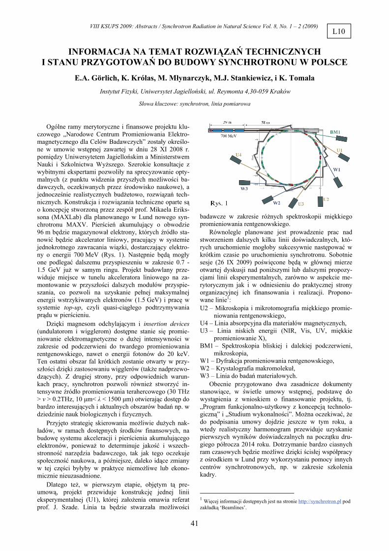
VIII KSUPS 2009: Abstracts / Synchrotron Radiation in Natural Science Vol. 8, No. 1 – 2 (2009)
41
INFORMACJA NA TEMAT ROZWIĄZAŃ TECHNICZNYCH I STANU PRZYGOTOWAŃ DO BUDOWY SYNCHROTRONU W POLSCE
E.A. Görlich, K. Królas, M. Młynarczyk, M.J. Stankiewicz, i K. Tomala
Instytut Fizyki, Uniwersytet Jagielloński, ul. Reymonta 4,30-059 Kraków
Słowa kluczowe: synchrotron, linia pomiarowa
Ogólne ramy merytoryczne i finansowe projektu klu-
czowego „Narodowe Centrum Promieniowania Elektro-magnetycznego dla Celów Badawczych” zostały określo-ne w umowie wstępnej zawartej w dniu 28 XI 2008 r. pomiędzy Uniwersytetem Jagiellońskim a Ministerstwem Nauki i Szkolnictwa Wyższego. Szerokie konsultacje z wybitnymi ekspertami pozwoliły na sprecyzowanie opty-malnych (z punktu widzenia przyszłych możliwości ba-dawczych, oczekiwanych przez środowisko naukowe), a jednocześnie realistycznych budżetowo, rozwiązań tech-nicznych. Konstrukcja i rozwiązania techniczne oparte są o koncepcję stworzoną przez zespół prof. Mikaela Eriks-sona (MAXLab) dla planowanego w Lund nowego syn-chrotronu MAXV. Pierścień akumulujący o obwodzie 96 m będzie magazynował elektrony, których źródło sta-nowić będzie akcelerator liniowy, pracujący w systemie jednokrotnego zawracania wiązki, dostarczający elektro-ny o energii 700 MeV (Rys. 1). Następnie będą mogły one podlegać dalszemu przyspieszeniu w zakresie 0.7 - 1.5 GeV już w samym ringu. Projekt budowlany prze-widuje miejsce w tunelu akceleratora liniowego na za-montowanie w przyszłości dalszych modułów przyspie-szania, co pozwoli na uzyskanie pełnej maksymalnej energii wstrzykiwanych elektronów (1.5 GeV) i pracę w systemie top-up, czyli quasi-ciągłego podtrzymywania prądu w pierścieniu.
Dzięki magnesom odchylającym i insertion devices (undulatorom i wigglerom) dostępne stanie się promie-niowanie elektromagnetyczne o dużej intensywności w zakresie od podczerwieni do twardego promieniowania rentgenowskiego, nawet o energii fotonów do 20 keV. Ten ostatni obszar fal krótkich zostanie otwarty w przy-szłości dzięki zastosowaniu wigglerów (także nadprzewo-dzących). Z drugiej strony, przy odpowiednich warun-kach pracy, synchrotron pozwoli również stworzyć in-tensywne źródło promieniowania terahercowego (30 THz > ν > 0.2THz, 10 μm< λ < 1500 μm) otwierając dostęp do bardzo interesujących i aktualnych obszarów badań np. w dziedzinie nauk biologicznych i fizycznych.
Przyjęto strategię skierowania możliwie dużych nak-ładów, w ramach dostępnych środków finansowych, na budowę systemu akceleracji i pierścienia akumulującego elektronów, ponieważ to determinuje jakość i wszech-stronność narzędzia badawczego, tak jak tego oczekuje społeczność naukowa, a późniejsze, daleko idące zmiany w tej części byłyby w praktyce niemożliwe lub ekono-micznie nieuzasadnione.
Dlatego też, w pierwszym etapie, objętym tą pre-umową, projekt przewiduje konstrukcję jednej linii eksperymentalnej (U1), której założenia omawia referat prof. J. Szade. Linia ta będzie stwarzała możliwości
badawcze w zakresie różnych spektroskopii miękkiego promieniowania rentgenowskiego.
Równolegle planowane jest prowadzenie prac nad stworzeniem dalszych kilku linii doświadczalnych, któ-rych uruchomienie mogłoby sukcesywnie następować w krótkim czasie po uruchomieniu synchrotronu. Sobotnie sesje (26 IX 2009) poświęcone będą w głównej mierze otwartej dyskusji nad poniższymi lub dalszymi propozy-cjami linii eksperymentalnych, zarówno w aspekcie me-rytorycznym jak i w odniesieniu do praktycznej strony organizacyjnej ich finansowania i realizacji. Propono-wane linie1: U2 – Mikroskopia i mikrotomografia miękkiego promie-
niowania rentgenowskiego, U4 – Linia absorpcyjna dla materiałów magnetycznych, U3 – Linia niskich energii (NIR, Vis, UV, miękkie
promieniowanie X), BM1 – Spektroskopia bliskiej i dalekiej podczerwieni,
mikroskopia, W1 – Dyfrakcja promieniowania rentgenowskiego, W2 – Krystalografia makromolekuł, W3 – Linia do badań materiałowych.
Obecnie przygotowano dwa zasadnicze dokumenty stanowiące, w świetle umowy wstępnej, podstawę do wystąpienia z wnioskiem o finansowanie projektu, tj. „Program funkcjonalno-użytkowy z koncepcją technolo-giczną” i „Studium wykonalności”. Można oczekiwać, że do podpisania umowy dojdzie jeszcze w tym roku, a wtedy realistyczny harmonogram przewiduje uzyskanie pierwszych wyników doświadczalnych na początku dru-giego półrocza 2014 roku. Dotrzymanie bardzo ciasnych ram czasowych będzie możliwe dzięki ścisłej współpracy z ośrodkiem w Lund przy wykorzystaniu pomocy innych centrów synchrotronowych, np. w zakresie szkolenia kadry.
1 Więcej informacji dostępnych jest na stronie http://synchrotron.pl pod zakładką ‘Beamlines’.
L10

VIII KSUPS 2009: Abstracts / Synchrotron Radiation in Natural Science Vol. 8, No. 1 – 2 (2009)
42
PIERWSZA LINIA NA POLSKIM SYNCHROTRONIE – SPEKTROSKOPIE
MIĘKKIEGO PROMIENIOWANIA RENTGENOWSKIEGO
J. Szade 1
, B. Orłowski 2, B. Kowalski
2, E.A. Görlich
3, K. Tomala
3 i P. Starowicz
3
1 Instytut Fizyki im. A. Chełkowskiego, Uniwersytet Śląski, ul. Uniwersytecka 4, 40-007 Katowice
2 Instytut Fizyki PAN, Al. Lotników 32/46; 02-668 Warszawa 3 Instytut Fizyki, Uniwersytet Jagielloński, ul. Reymonta 4,30-059 Kraków
Słowa kluczowe: synchrotron, linie ekperymentalne
Zgodnie z decyzjami finansowymi w pierwszym
etapie budowy polskiego synchrotronu w Krakowie
zostanie oddana do użytku jedna linia eksperymentalna.
Ma to być linia poświęcona spektroskopiom miękkiego
promieniowania rentgenowskiego, głównie spektroskopii
fotoelektronów.
Planujemy, żeby źródłem promieniowania był
ondulator umożliwiający zmianę polaryzacji
promieniowania i zapewniający uzyskanie zakresu
energii 50-1500 eV. Monochromator powinien zapewnić
rozdzielczość energetyczną E/ΔE∼104.
Linie o podobnych do planowanych u nas paramet-
rach można znaleźć na prawie wszystkich światowych
synchrotronach trzeciej generacji. Polski synchrotron
będzie prawdopodobnie budowany w oparciu o nowe
koncepcje rozwijane w ośrodku Max-Lab w Lund w
Szwecji. Pierwsza linia na polskim synchrotronie będzie
zbliżona pod względem parametrów i technik
badawczych do linii I311 i I511 pracujących obecnie
przy pierścieniu akumulacyjnym MAX II.
Podstawowymi technikami badawczymi będą
spektroskopia fotoelektronów i spektroskopia absorp-
cyjna. Konstrukcja linii powinna umożliwić poszerzenie
w przyszłości możliwości badawczych o takie techniki
jak spektromikroskopia i spektroskopia emisyjna.
Stacja pomiarowa powinna umożliwić badania
przy użyciu takich metod jak:
� Rezonansowa spektroskopia fotoelektronów
- typu Fano pozwalająca na określenie wkładu stanów
elektronowych pochodzących od różnych
pierwiastków (np. 4f metali ziem rzadkich) do pasma
walencyjnego oraz badanie reakcji chemicznych na
powierzchni.
� Spinowo rozdzielcza spektroskopia fotoelektronów
- pozwalająca na powiązanie polaryzacji spinowej z
konkretnymi stanami elektronowymi, konieczny
będzie dodatkowy detektor (np. Motta) przy
spektrometrze fotoelektronów.
� Absorpcja promieniowania rentgenowskiego
(XAS) -
- badanie krawędzi absorpcji ziem rzadkich, metali
przejściowych, tlenu, krzemu i innych pierwiastków
w zakresie miękkiego promieniowania X, pomiar w
trybach TEY (Total Electron Yield) and TFY (Total
Fluorescence Yield).
Dzięki możliwości zmiany polaryzacji
promieniowania można będzie wykonywać badania
dichroizmu magnetycznego w absorpcji i fotoemisji przy
zachowaniu warunków bezpieczeństwa dla analizatora
fotoelektronów ograniczających wartość pola
magnetycznego wewnątrz komory pomiarowej.
Manipulator powinien umożliwiać pomiary w
szerokim zakresie temperatur, co najmniej 20-1000 K.
Dzięki sześciu osiom obrotu będzie częściowo możliwe
zastosowanie rozdzielczej kątowo spektroskopii
fotoelektronów (ARPES) przy zastosowaniu
odpowiednich soczewek analizatora i modu pracy.
Stosunkowo wysoka wartość dolnej energii granicznej
stawia wysokie wymagania dla analizatora
fotoelektronów, ale szybki rozwój w tej dziedzinie
powinien umożliwić przynajmniej częściowo pomiary w
trybie ARPES. Pomiary takie pozwalają na badanie
struktury pasmowej. Możliwe będzie tez badanie
dyfrakcji fotoelektronów – źródła informacji o strukturze
krystalicznej powierzchni.
Przewidujemy instalację odpowiednich komór
preparacyjnych, gdzie znajdą się działo jonowe, łupacz
kryształów oraz komórki efuzyjne do naparowania
cienkich warstw.
Stacja pomiarowa pierwszej linii eksperymentalnej
ma mieć charakter raczej uniwersalny ze spektroskopią
fotoelektronów jako techniką dominującą. Pozwoli to na
prowadzenie badań w wielu rozwijanych już dziś w
Polsce dziedzinach, takich jak:
� Fizyka silnie skorelowanych elektronów,
� Fizykochemia powierzchni, zjawiska katalizy,
badania reakcji na powierzchni,
� Nowe materiały - cienkie warstwy, heterostruktury,
materiały dla spintroniki,
� Magnetyzm powierzchni,
� Biomateriały,
� Mineralogia i geologia. �
L11

VIII KSUPS 2009: Abstracts / Synchrotron Radiation in Natural Science Vol. 8, No. 1 – 2 (2009)
43
ELECTRONIC STATES OF COLLOSAL MAGNETORESISTIVE MANGANITES La0.67Pb0.33 Mn1-xFexO3 FROM PHOTOEMISSION
SPECTROSCOPY
M. Kowalik 1,2*, R. Zalecki 1, and A. Kołodziejczyk 1
1 Faculty of Physics and Applied Computer Science, AGH University of Science and Technology,
Al. Mickiewicza 30, PL 30-059, Kraków, Poland 2 Department of Physics, Rzeszów University of Technology, Al. Powstańców Warszawy 6, PL 35-959 Rzeszów, Poland
Keywords: manganites, photoemission, electronic states
*) e-mail: [email protected]
The electron photoemission spectra of the valence
bands and the core level states of manganese perovskite La0.67Pb0.33(Mn1-xFex)O3 with x = 0, 0.01, 0.03, 0.06, 0.1 and 0.15 were measured by the Ultraviolet and the X-ray Photoemission Spectroscopy (UPS/XPS) below and above the metal-insulator transition. X-ray diffraction showed that the compounds were phase pure. The magnetic and resistance measurements exhibited the large colossal magnetoresistance behaviour around the metal − insulator transitions. The common feature of the UPS spectra was the two-peak structure at about -4.0 and -6 eV below the upper edge of the valence band (Fig. 1). The same was observed in Refs. [1, 2].
-12 -10 -8 -6 -4 -2 0 2
-3 -2 -1 0
1% Fe 10% Fe 15% Fe
inte
nsity
/ ar
b. u
.
Binding energy / eV
Figure 1. UPS spectra of La0.66Pb0.33Mn1-xFex03 for x = 0.01, 0.1, 0.15 at room temperature.
The insulating energy gaps were estimated at room temperature to be about 1.7÷2.0 eV and were composition dependent. Total energy scan and low binding energy spectra of X-ray (XPS- Al, Mg Kα) as well as the Mn 2p- and 3s- core-level spectra were also measured and analyzed (Fig. 2). Comparison of the spectra with the band structure calculations and with the high-resolution spectra measured at synchrotron radiation for Ca- and Ce- substituted manganites [3, 4] revealed the strong hybridization of the Mn 3d and of the O 2p states between -3 and -7 eV and no oxygen states between 0 and -2 eV where the Mn- 3d states play predominant role. Reasons for this behaviour were
discussed taking into account our previous analysis of UPS/XPS spectra of other manganese perovskites [1, 2].
Acknowledgements: The samples were prepared within the collaboration with Professor Gritzner group from the Keppler University in Linz, Austria. This was supported by the Faculty of Physics and Applied Computer Science, AGH University of Science and Technology, Cracow, Poland.
References
[1] R. Zalecki, A. Kołodziejczyk, C. Kapusta, K. Krop, "Electronic states of La1-xCaxMnO3 from photoelectron spectroscopy", J. Alloys Compds. 328 (2001) 175–180.
[2] R. Zalecki, A. Kołodziejczyk, C. Kapusta, G. Zaręba, J. Fink-Finowicki, M. Baran, R. Szymczak, H. Szymczak, "Photoemission band structure of La0.7(Ca, Ce)0.3MnO3 thin films and a La0.9Ca0.1CoO3 crystal", J. Alloys Compds. 442 (2007) 296–298.
[3] D.N. McIlroy, C. Waldfried, J. Zhang, J.W. Choi, F. Foong, S.H. Liou, P.A. Dowben, "Comparison of the temperature-dependent electronic structure of the perovskites La0.65A0.35MnO3 (A=Ca, Ba)", Phys. Rev. B 54 (1996) 17438.
[4] S.W. Han, J.-S. Kang, K.H. Kim, J.D. Lee, J.H. Kim, S.C. Wi, C. Mitra, P. Raychaudhuri, S. Wirth, K.J. Kim, B.S. Kim, J.I. Jeong, S.K. Kwon, B.I. Min, "Photoemission and x-ray absorption spectroscopy study of electron-doped colossal magnetoresistive manganite La0.7Ce0.3MnO3 films", Phys. Rev. B 69 (2004) 104406.
-800 -600 -400 -200 0
-660 -655 -650 -645 -640 -635
Mn:
3p
O:K
L
Mn:
LMM
Pb:4
p3/2
O:1
s
Mn:
3s
Mn:
2p
La:4
d
La:4
p
La:3
d
Pb:5
s, 4
f
Pb:4
d
Pb:
4p1/
2
inte
nsity
/ ar
b. u
.
Binding energy / eV
Mn: 2p
Figure 2. The total X-ray (Mg, Kα) spectra of La0.66Pb0.33Mn03 with the core-level and Auger lines indicated at room temperature. Inset: the Mn 2p core-level spectrum taken with Al-Kα without background.
P 01

VIII KSUPS 2009: Abstracts / Synchrotron Radiation in Natural Science Vol. 8, No. 1 – 2 (2009)
44
DEFECT STRUCTURE FORMED AT DIFFERENT STAGES
OF GROWTH PROCESS IN ERBIUM, CALCIUM AND HOLMIUM DOPED
YVO4 CRYSTALS
A. Malinowska 1*, E. Wierzbicka 1, M. Lefeld-Sosnowska 2, K. Wieteska 3, W. Wierzchowski 1
T. Łukaszewicz 1, M. Świerkowicz 1, and W. Graeff 4
1Institute of Electronic Materials Technology, ul. Wólczyńska 133, 01-919 Warsaw, Poland
2Institute of Experimental Physics, University of Warsaw, ul. Hoża 69, 00-681 Warsaw, Poland 3Institute of Atomic Energy POLATOM, 05-400 Otwock-Świerk, Poland
4HASYLAB at DESY, Notkestr. 85, 22-603 Hamburg, Germany
Keywords: YVO4 crystals, crystallographic defects, X-ray diffraction topography
*) e-mail: [email protected]
Yttrium orthovanadate (YVO4) is one of the most
important laser host materials due to high quantum
efficiency and low excitation level when doped with rare
earth ions. It is especially useful in micro-laser systems
pumped with semiconductor laser diodes. In these
applications the crystals should be highly doped with the
rare earth elements as erbium or holmium. YVO4 is of
zircon tetragonal structure with space group I41/amd and
lattice parameter a = b = 0.712 nm and c = 0.629 nm.
The crystallographic structure enables efficient
introduction of the required ions. Some recent results
concerning growth of YVO4 are described in Refs. [1-3].
The investigated samples were cut out from different
regions of a number of Czochralski grown YVO4
crystals, doped with erbium, holmium and calcium. The
concentrations of the introduced dopants were 0.5 at. %,
5 at. %, and 0.4 at. %, respectively. Some samples were
cut out from the regions of the spiral growth, which is
one of the most important problems in technology of the
crystals. The X-ray topographic methods exploring both
conventional and synchrotron X-ray sources were used as
the principal methods of characterization. The
conventional X-ray Lang topographs were obtained both
in transmission and back reflection geometry. The
synchrotron investigations were performed in white
X-ray beam and included taking the topographs through
a fine mesh with a wire spacing of 0.7 mm, enabling
precise evaluation of the lattice deformation.
Despite very large concentrations of the dopants the
topographs obtained with all used methods did not reveal
any segregation fringes. That proves a high homogeneity
of chemical composition, corresponding to the
segregation coefficient close to the unity. The main
defects revealed in the topographs were the numerous
subgrain boundaries, which density and character were
different in various regions of the crystals. In the
examined crystals we observed much lower density
(< 104 cm-2) of weak point-like contrasts (most probably
attributed to dislocation outcrops), than in the case of
formerly investigated undoped YVO4 crystal [4].
The values and directions of lattice misorientation
connected with the subgrain boundaries were most
precisely revealed by the synchrotron back-reflection
projection topographs exposed through a mesh, and to
some extend by the synchrotron section topographs, and
by the Lang conventional topographs as well. The
evaluated misorientation values were in the range of
0.10.7°.
References
[1] S. Wu, G. Wang, J. Xie, X. Wu, G. Li, "Growth of large
birefringent YVO4 crystal", J. Cryst. Growth 249 (2003)
176–178.
[2] H. Zhang, Y. Yu, Y. Cheng, J. Liu, H. Li, W. Ge, X. Cheng,
X. Xu, J. Wang, M. Jiang, "Growth of YbVO4
stoichiometric crystal", J. Cryst. Growth 283 (2005) 438–
443.
[3] Y. Yu, Y. Cheng, H. Zhang, J. Wang, X. Cheng, H. Xia,
"Growth and thermal properties of YbVO4 single crystal",
Mater. Lett. 60 (2006) 1014–1018.
[4] K. Wieteska, W. Wierzchowski, E. Wierzbicka, A.
Malinowska, M. Lefeld-Sosnowska, T. Łukasiewicz, W.
Graeff, "X-Ray topographic studies of defect structure in
YVO4 crystals", Acta Phys. Polon. A 114 (2008) 455–461.
P 02

VIII KSUPS 2009: Abstracts / Synchrotron Radiation in Natural Science Vol. 8, No. 1 – 2 (2009)
45
SYNCHROTRON RADIATION AS A TOOL OF BIOCHEMICAL ANALYSIS IN BRAIN CANCERS
M. Szczerbowska-Boruchowska 1*, M. Lankosz 1, A. Smykla1, and D. Adamek 2
1 Faculty of Physics and Applied Komputer Science, AGH University of Science and Technology,
Al. Mickiewicza 30,30-059 Krakow, Poland 2 Institute of Neurology, Medical College, Jagiellonian University
Botaniczna Str. 3, 31-503 Krakow, Poland
Keywords: trace elements, oxidation states of elements, biomolecules, brain cancers
*) e-mail:[email protected]
The recent development of synchrotron radiation based microprobe beamlines has enabled spatially resolved XRF (X-ray fluorescence), XANES (X-ray absorption near edge structure spectroscopy) and FTIRM (Fourier transform infrared microspectroscopy) at cellular and subcellular level. Synchrotron radiation XRF (SR-XRF) microprobe analysis as a multielemental analytical method was applied to simultaneous imaging of chemical elements in human brain tumors. Micro-XANES technique which gives information primarily about geometry and oxidation state was used to determine the chemical state of Fe and S in brain gliomas. FTIRM that provides direct information on the molecular composition of the tissue was applied to determine organic composition of brain cancers. The SR-XRF and Fe XANES measurements were performed at the bending magnet beamline L at HASYLAB. Micro-imaging of sulfur oxidation states using XANES measurements was carried out on beamline ID21 at ESRF. FTIRM measurements were performed on SMIS beamline at the synchrotron SOLEIL.
The SR-XRF research allowed detection of P, S, Cl, K, Ca, Fe, Cu, Zn, Br and Rb in human brain tumors. The topographic analysis enabled to determine two-dimensional distribution of elements in characteristic tissue structures in case of cancerous tissues. The Fe XANES analysis in selected points of the tissue showed
that all the XANES spectra obtained for the brain glioma samples are situated between the spectra measured for reference materials containing Fe in the second and third oxidation state (Fig. 1). However, taking into account inhomogeneity of the tissue structure the knowledge based on the results from random points seems to be insufficient. Therefore, the micro-imaging of iron oxidation states were performed. The mapping of different chemical form of iron allowed finding areas were bivalent or trivalent iron compounds were dominant.
The results of S XANES analysis showed that cancer cells accumulate sulfur mainly as sulfide (S2-) form. The preliminary results indicated also higher accumulation of this form of sulfur in glioma of IV grade of malignancy in comparison with the samples of II grade neoplasms. The presence of sulfate (S+6) species was revealed in histological structures outside the cancer cells. The sulfite (S+4) form of sulfur was not detected in the scanned areas of tissue.
In the FTIRM the tissue areas were mapped to generate two-dimensional images of the main biological molecules of interest. Integrated intensities of selected bands were extracted after raster scanning of the sample. The obtained IR maps were compared with the microscopic view of the slices prepared previously for histopathological examination. It allowed determining
biochemical composition of the structures of different types of cancerous tissue. The preliminary studies showed differences in biomolecular composition between the studied cases of brain tumors. It will be used in the future (when statistically reliable number of samples will be investigated) to identify biological molecules typical for various types of brain cancers.
Acknowledgements: The authors are indebted to Dr. P. Dumas (SOLEIL), Dr. J. Susini (ESRF) and Dr. K. Rickers-Apple (HASYLAB) for their assistance. Support of the Ministry of Science and High Education, Warsaw, Poland and the following grants Ministry of Science and High Education, Warsaw, Poland; Grant Number: 155/ESR/2006/03, DESY/304/2006 as well as European Community; Grant Number: RII3-CT-2004-506008 (IA-SFS) are acknowledged.
P 03
Figure 1. The Fe XANES spectra different cases of glioma tissues (g1-g4) and reference materials.

VIII KSUPS 2009: Abstracts / Synchrotron Radiation in Natural Science Vol. 8, No. 1 – 2 (2009)
46
COMPLEX STRUCTURE OF Mg2Al3 β AND β’ PHASES
J. Wolny 1*
, M. Duda 1
, and B. Kozakowski 1
1 Faculty of Physics and Computer Science, AGH University of Science and Technology,
al. Mickiewicza 30, 30-059 Kraków, Poland
Keywords: Mg2Al3, Samson phase, hexagonal layers
*) e-mail: [email protected]
The Samson phase structure is one of the most
complex intermetallic structures. The first description of
the β-Mg2Al3 structure was provided by Samson [1] in
60’. Because of its complexity and potential new
technical applications, during the last few years the
Samson structure aroused considerable interest among
crystallographers. A good example of that interest is a
review publication, written by 36 authors from 15
leading European laboratories [2].
Its cubic elementary cell (Fd-3m, no. 227 space
group) contains 1168 atoms which are distributed over
1832 atomic positions. About 75% of atoms (879 to be
exact) form the framework of the structure (skeleton
atoms). The framework is made up of Samson’s positions
which are occupied by atoms with SOF equal to 1. The
remaining 289 (25%) atoms partially occupy 953
positions with the average occupation probability of
30%. They form clusters arranged in an elementary cell
in a tetrahedral lattice. Their structure has been described
in detail in [2 and the following references] and in [3].
The lattice constant of the Samson structure is gigantic:
a = 2.8242(1) nm. At a temperature of 214°C, the
structure undergoes a phase transformation to the
rhombohedral β’-Mg2Al3 (space group R3m, no. 160,
which is a subgroup of the Fd-3m group - index 4) with
a = 1.9968(1) nm, c = 4.89114(8) nm. It should be
pointed out that the constant c of a rhombohedral
structure is practically equal to the length of the diagonal
of the cubic structure rhombcubic
nm89166,43 ca ≈=. The near
equivalence in length between the c axis of the
rhombohedral β’-Mg2Al3 structure and the diagonal of
the cubic β-Mg2Al3 is a consequence of lattice
transformation connecting the hR cell of the β’-phase to
the F cell of the β-phase.
Comparison of two different types of Mg2Al3
structure – cubic β and rhobohedral β’ ones – leads to the
conclusion that all skeleton atoms of a Samson structure
don’t change their position during the phase
transformation. The skeleton atoms of a Samson phase
lie within hexagonal layers [4]. These layers form three
structural domains shifted with respect to each other by
1/3 of the length of the main diagonal of the cubic unit
structure.
Besides within a hexagonal layer the length of every
shift vector is a multiple of about 1/7 of the distances
characteristic for hexagonal structures. Once the shift
vectors were found, one could describe the structure as a
modulated one.
Figure 1. Eighteen layers forming a structural domain.
Positions of Al and Mg atoms within the consecutive
hexagonal layers for a structural domain of the Samson
structure. Aluminium atoms take the hexagonal
positions A, B, C. Magnesium atoms occupy positions
which are shifted with respected to the Al layers.
References
[1] S. Samson, "The crystal structure of the phase ß-Mg2Al3",
Acta Crystallogr. 19 (1965) 401–413.
[2] M. Feuerbacher et al., "The Samson phase, ß-Mg2Al3
revisited", Z. Kristallogr. 222 (2007) 259–288.
[3] W. Sikora et al., "Symmetry analysis in the investigation of
clusters in complex metallic alloys", J. Phys.: Conf. Ser.
104 (2008) 012023.
[4] J. Wolny, B. Kozakowski, M. Duda, J. Kusz, "Stacking of
hexagonal layers in the structure of β-Mg2Al3", Philos.
Mag. Lett. 88 (2008) 501–507.
P 04

VIII KSUPS 2009: Abstracts / Synchrotron Radiation in Natural Science Vol. 8, No. 1 – 2 (2009)
47
STRUCTURAL STUDIES
OF HEAVILY TRANSITION METAL IMPLANTED ZnO
E. Dynowska 1, W. Szuszkiewicz
1, C. Ziereis
2, J. Geurts
2, S. Müller
3, C. Ronning
4,
J. Domagala 1, P. Romanowski
1, and W. Caliebe
5
1 Institute of Physics, Polish Academy of Sciences, al. Lotników 32/46, 02-668 Warszawa, Poland
2 Physikalisches Institut, Universität Würzburg, am Hubland, 97074 Würzburg, Germany 3 II. Physikalisches Institut, Universität Göttingen, Friedrich-Hund-Platz 1, 37077 Göttingen, Germany
4 Institut für Festkörperphysik, Universität Jena, Max-Wien-Platz 1, 07743 Jena, Germany 5 Hasylab at DESY, Notkestr. 85, D-22603 Hamburg, Germany
Keywords: diffraction, ZnO, implantation
The study of ZnO alloyed with transition metals (TM) has been stimulated by theoretical predictions of room temperature ferromagnetism for these compounds [1, 2]. One of the methods for the incorporation of TM into ZnO is ion implantation connected with proper thermal treatment. The magnetic properties of ZnO:TM compounds depend on their crystal structure after such procedure.
In this work we report the results of structural characterization of ZnO crystals implanted with 16 at.% of Mn, Co, Fe and Ni ions and annealed at 900°C in air. The X-ray structural characterization was performed using synchrotron radiation at the W1.1 beamline at DESY-Hasylab. The monochromatic X-ray beam of wavelength λ = 1.54056 Å was used. Two modes of measurement were applied: symmetrical ω-2θ scan and coplanar 2θ scan in the glancing incidence geometry.
Fig. 1 shows the X-ray ω-2θ patterns for Mn- and Co-implanted and annealed ZnO samples, respectively. The interpretation of these patterns leads to different results for these two samples. The main effect of annealing of Mn-implanted ZnO sample is the creation of monocrystalline inclusion of ZnMn2O4 tetragonal phase (a = 5.7204 Å and c = 9.2450 Å) - the (101) lattice planes of this phase are parallel to the (0001) lattice planes of ZnO matrix. Moreover, the left-side asymmetry of 000l peaks of ZnO matrix (Fig. 1a) indicates the presence of the solid solution Zn1-xMnxO phase with very low quantity of Mn corresponding to x ≈ 0.005.
In the pattern presented in Fig. 1b the very strong peaks originating mainly from the bulk ZnO and several much weaker ones are visible. The detailed analysis of the peaks originated from ZnO exhibits the right-side asymmetry of these peaks that confirms a creation of the solid solution Zn1-xCoxO with estimated composition x ≈ 0.075. The weak peaks visible in the pattern are probably caused by a trace inclusions of some single crystalline phases with crystallographic orientation closely connected with (0001) planes of ZnO. Only three weak reflections have been identified up to now: two of them as belonging to the elemental Zn and one can be attributed to the ZnCo2O4 or Co3O4 phases – these phases have very similar crystal structure.
(a)
30 40 50 60 70 80
0
2
4
6
8
10
404 Z
nM
n2O
4
303 Z
nM
n2O
4
202 Z
nM
n2O
4
0004 Z
nO
0002 Z
nO
ZnO impl. Mn (16%)
ω - 2θ scan
log
in
ten
sit
y
2θ (deg)
(b)
20 30 40 50 60 70 80
2
4
6
8
10
0004 Zn
0002 Zn
222 ZnCo2O
4
or Co3O
4
0004
ZnO
ZnCoO
0002
ZnO
ZnCoO
ZnO impl Co (16%)
ω - 2θ scan
2θ (deg)
log
in
ten
sit
y
Figure 1. The X-ray ω-2θ diffraction patterns of
ZnO:Mn (a) and ZnO:Co (b) samples after annealing.
Concluding, we can state that in the case of ZnO:Mn majority of Mn incorporated by implantation into bulk sample of ZnO after annealing has been located in ZnMn2O4 spinel phase, while in ZnO:Co majority of Co have been built into ZnO matrix creating the ternary compound Zn0.925Co0.075O.
Acknowledgements: This work was partially supported by the
European Community - Research Infrastructure Action under
the FP6 "Structuring the European Research Area" Programme
(through the Integrated Infrastructure Initiative "Integrating
Activity on Synchrotron and Free Electron Laser Science",
Contract RII3-CT-2004-506008).
References
[1] T. Dietl, H. Ohno, F. Matsukura, J. Cibert, D. Ferrand,
"Zener model description of ferromagnetism in zinc-blende
magnetic semiconductors", Science 287 (2000) 1019.
[2] K. Sato, H. Katayama-Yoshida, "Stabilization of
ferromagnetic states by electron doping in Fe-, Co- or Ni-
doped ZnO", Jpn. J. Appl. Phys. 40 (2001) L334.
P 05

VIII KSUPS 2009: Extended abstracts / Synchrotron Radiation in Natural Science Vol. 8, No. 1 – 2 (2009)
48
DYNAMIC SAXS CORRELATION AS METHOD OFSTRUCTURAL RESEARCH
H. Grigoriew 1*, L. Wiegert 2, and A. Boczkowska 3
1 Institute of Nuclear Chemistry and Technology, 03-195 Warsaw, Poland
2 ESRF, Grenoble 38043 Cedex, France 3 Faculty of Materials Science, Warsaw University of Technology, 02-507 Warsaw, Poland
Keywords: XPCS method, structural dynamics, magnetic field
*) e-mail: [email protected]
Composite-type material consisted of polyurethane gel, and carbonyl iron (CI) of 7 μm size spheres. The gel constituents were: MDI/OAE+DCDA with molar ratio 70/30. The material was processed with 11.5 vol.% of CI under magnetic field, during 24 h at 25ºC.
SEM images of the composite showed short chains of CI formed inside the material.
- XPCS (X-ray Photon Correlation Spectroscopy) measurements were performed on the Troika beamline (ID10A) of the ESRF in SAXS configuration. The meaurements depending on time (t) and angle (q), using X-beam wavelength of 1.745 Å, and detector type CCD were used. The sample was placed between electromagnet poles with magnetic lines direction perpendicular to the X-beam and parallel to the sample surface and CI chains inside it. Measurements were performed for: 0, 300 and 600 mT. It occurred that correlation of scattered intensity took place in the time range: from 5×10² to 100×102 sec.
- Correlation curves, g2(t): The correlation function g2(t), according to the formula g2(t)=‹I(to+t)I(to)›/‹I(to)
2› was obtained from I(t, q) CCD measurements using masks to get them in directions: parallel (par), isotropic (iso) and perpendicular (per) to the magnetic field lines.
- The reference curves at 0 mT are of extremely slow dynamics behavior with correlation reached for about 104 sec and of weak differentiation between the measurement directions. For 300 mT, the correlation is faster (~ 1.2×10³ sec) with the dependence on different directions. For 600 mT the correlation is the fastest, of less than 103 sec.
- Correlation rates, Γ(q). The correlation rates, Γ(q), were found by fitting exponential function: y = a e 2Γ x to the subsequent g2 (t) curves, in their region of correlation behavior. Fig. 1 shows Γ(q) curves for subsequent magnetic field value, with sets of three curves for each directions (par, iso and per). When magnetic field increases, from 0 through 300 to 600 mT, correlation rate also increases. It occurred that the magnetic field essentially influences the correlation rate, up to ten times (Fig. 1). Besides, within each set the highest curve is for direction parallel to the magnetic field (par), the lowest one for direction perpendicular (per) and the middle one is for isotropic (without mask) measurement. The straight-line shape of all Γ(q) curves are of no significant deviations. The
correlation process is thus not due to structural reorganization on measured length scale.
Figure 1. Correlation rates Γ(q) for different magnetic field values. At each three curve set: bottom – perpendicular, middle – isotropic, top – parallel to the field lines. In the case of linear Γ(q) shape, the dependence it on
diffusion coefficient is: Γ(q) = D × q. The D [Å/sec] values were found from slope of straight lines fitted to Γ(q) (Table 1).
- For the reference curves for 0 mT the very moderate values of the Γ(q),and D as well as no differentiation from direction seem to be an evidence of very strong structure.
- For the middle value of the field (300 mT), the same parameters are strongly dependent on the magnetic field direction and are of much bigger values (Fig. 1 and Table 1). Here dependence on the material dynamics from direction of the outer magnetic field is very clear, with strongly privileged parallel direction (par).
- But for the magnetic field of 600 mT, despite the highest correlation rate, the dependence on magnetic field direction became weak, as well as D values (Fig. 1 and Table 1). Simultaneously, on the Γ(q) curves the bigger fluctuation around the fitted straight lines are observed. There probably mechanism of dynamics behavior altered.
Table 1. Diffusion coefficients, D [Å /sec].
Reference [1] J. Lal, D. Abernathy, L. Auvray, O. Diat, G. Gruebel,
"Dynamics and correlations in magnetic colloidal systems studied by X-ray photon correlation spectroscopy", Eur. Phys. J. E4 (2001) 263.
P 06

VIII KSUPS 2009: Abstracts / Synchrotron Radiation in Natural Science Vol. 8, No. 1 – 2 (2009)
49
BADANIA ABSORPCYJNE ZMODYFIKOWANYCH CHEMICZNIE CHITOZANÓW Z ŻELAZEM
M.T. Klepka 1*, K. Lawniczak-Jablonska 1, and A. Wolska 1
1 Instytut Fizyki Polskiej Akademii Nauk, al. Lotników 32/46, 02-668 Warszawa
Słowa kluczowe: chitozan, absorpcja, synchrotron
*) e-mail: [email protected]
Kompleksy metal-chitozan zawierające metale przejściowe wzbudzają zainteresowanie wielu grup naukowych. Na intensywne badania tych materiałów mają wpływ ich nietuzinkowe właściwości. Chitozan jest produktem deacetylacji chityny (Rys. 1), a ta jest jednym z głównych składników pancerzy skorupiaków morskich. Oba te materiały są liniowymi polimerami. Chitozan jest materiałem pochodzenia naturalnego, a więc jest nietoksyczny, biokompatybilny, bioaktywny oraz ulega łatwej biodegradacji. Szczególne zainteresowanie budzi jednak zdolność chitozanu do związywania w swoją strukturę metali zarówno ciężkich jak i toksycznych [1]. Polimer ten dzięki swoim własnościom jest już wykorzystywany w wielu gałęziach przemysłu, a możliwości jego zastosowań ciągle się powiększają [2].
Rysunek 1. Deacetylacja chityny.
Obecnie trwają badania nad zastosowaniem kompleksów żelazo-chitozan jako biotransportera leków z kontrolowanym uwalnianiem substancji aktywnych. Możliwe jest to, gdyż chitozan po związaniu jonu metalu wykazuje właściwości magnetyczne [3]. Chitozan znajduje także inne zastosowania w biomedycynie dzięki takim cechom jak działanie bakteriobójcze, immunologiczne czy przeciwnowotworowe [4, 5]. W celu zwiększenia właściwości adsorpcyjnych chitozanu stosuje się różnorodne modyfikacje chemiczne, jak sieciowanie łańcuchów polimeru czy przyłączanie grup aktywnych, jak np. –COOH.
Pomimo dużego zainteresowania tymi materiałami i wieloma doniesieniami literaturowymi o jego właściwościach i zastosowaniach, wciąż nie jest jasny
mechanizm związywania metali przez te polimery. Podstawową techniką stosowaną do określania pozycji atomów metalu w tych materiałach jest spektroskopia Mössbauera, nie pozwala ona jednak na określenie rodzaju sąsiadujących atomów, w przeciwieństwie do rentgenowskiej spektroskopii absorpcyjnej.
Zaprezentowane zostaną wyniki, uzyskane na podstawie badań absorpcji promieniowania rentgenowskiego, dla kilku kompleksów żelazo-chitozan poddanych różnym modyfikacjom chemicznym.
Pomiary absorpcyjne dla krawędzi K żelaza zostały przeprowadzone na synchrotronie DORIS III, stacja A1, HASYLAB, DESY. Przeprowadzono je wykorzystując metodę fluorescencyjną, korzystając z siedmioelementowego detektora krzemowego.
Rentgenowska spektroskopia absorpcyjna ze względu na wysoką czułość i selektywność pierwiastkową okazuje się być bardzo dobrym narzędziem do badań nieuporządkowanych strukturalnie układów.
Podziękowania: Autorzy składają podziękowanie za finansowanie uzyskane dzięki grantowi Ministerstwa Nauki i Edukacji N202-052-32/1189 oraz DESY/HASYLAB i Unii Europejskiej w ramach projektu RII3-CT-2004-506008 (IA-SFS).
Literatura
[1] N.V. Majeti, K. Ravi, "A review of chitin and chitosan applications", React. Funct. Polym. 46 (2000) 1–27.
[2] M.F.A. Goosen, Applications of chitin and chitosan (CRC Press 1996).
[3] M.T. Klepka, N. Nedelko, J.M. Greneche, K. Ławniczak-Jabłońska, I.N. Demchenko, A. Ślawska-Waniewska, C.A. Rodrigues, A. Debrassi, C. Bordini, "Local atomic structure and magnetic ordering of iron in Fe-chitosan complexes", Biomacromolec. 9 (2008) 1586–1594.
[4] X. Wang, Y. Du, H. Liu, "Preparation, characterization and antimicrobial activity of chitosan-Zn complex", Carbohyd. Polym. 56 (2004) 21–26.
[5] K. Kurita, "Chitin and chitosan: functional biopolymers from marine crustaceans", Marine Biotechnol. 8 (2006) 203–226.
P 07

VIII KSUPS 2009: Extended abstracts / Synchrotron Radiation in Natural Science Vol. 8, No. 1 – 2 (2009)
50
LOKALNE OTOCZENIE JONÓW MANGANU
IMPLANTOWANYCH W KRYSZTAŁACH GaSb
A. Wolska 1*
, K. Lawniczak-Jablonska 1
, M.T. Klepka 1
, A. Barcz 1,
A. Hallen 2
, and D. Arvanitis 3
1 Institute of Physics PAS, al. Lotników 32/46, 02-668, Warsaw, Poland
2 Royal Inst. of Technology, Dept. of Microelectronics and Applied Physics, Box 226, SE 164 40 Kista, Sweden 3 Department of Physics and Materials Science, Uppsala University, Box 530, 75121 Uppsala, Sweden
Keywords: MnSb, GaSb, implantation
*) e-mail: [email protected]
Wśród materiałów ferromagnetycznych, które mogą znaleźć zastosowanie w urządzeniach wykorzystujących spin, najczęściej wymienia się związek GaMnAs. Intensywnie bada się zarówno jednorodny potrójny stop, jak i wytrącenia MnAs w matrycy GaAs. Co więcej, okazało się, że ferromagnetyczne nanowytrącenia MnAs można uzyskać nie tylko poprzez hodowlę metodą MBE, ale także poprzez implantację jonów Mn do kryształów GaAs [1-3]. Ma to istotne znaczenie praktyczne, gdyż implantacja jest metodą tańszą w masowej produkcji. Innym typem wytrąceń o potencjalnie interesujących własnościach magnetycznych są wytrącenia MnSb. Objętościowy związek MnSb ma temperaturę Curie 587 K i magnetyzację nasycenia w temperaturze pokojowej 710 emu/cm3. Wykazano też, że warstwy Mn1-xSbx hodowane na podłożu GaAs osiągają temperaturę Curie 620 K [4, 5]. Umiejętność otrzymywania ich poprzez implantację ułatwiłaby potencjalne zastosowania przemysłowe. Dlatego więc znalezienie optymalnych warunków do uzyskiwania wytrąceń o pożądanych własnościach jest szczególnie istotne.
Próbki badane w prezentowanej pracy zostały przygotowane poprzez implantację kryształów GaSb jonami Mn. Energia jonów wynosiła 10 keV dla zestawu próbek oznaczonego S oraz 150 keV dla zestawu oznaczonego GS. Dawki jonów użyte dla zestawu S były następujące: 1×10¹⁶ Mn/cm2 (S1), 2×10¹⁶ Mn/cm2 (S2) oraz 3×10¹⁶ Mn/cm2 (S3). Dla zestawu GS dawka wynosiła 1.7×10¹⁷ Mn/cm2. Pierwszy zestaw był następnie wygrzany w piecu próżniowym przez 10 min. w temperaturze 650ºC. W przypadku zestawu drugiego jedna próbka pozostała niewygrzana (GS), kolejna była wygrzana w atmosferze argonu przez 5 min. w 350ºC (GSRf), kolejne dwie zaś wygrzewano w parach antymonu w 400ºC przez 48 h (GS4) oraz 600ºC przez 2 h (GS6).
Pomiary absorpcji promieniowania synchrotronowego zostały przeprowadzone w laboratorium Hasylab na stacjach Cemo i E4. Wykonano pomiary widm EXAFS na krawędzi K manganu na próbkach schłodzonych do temperatury ciekłego azotu i przy użyciu detektora fluorescencyjnego. Dodatkowo metodą transmisyjną zmierzono widma komercyjnych proszków MnSb oraz MnO. Uzyskane dane były
analizowane przy pomocy programów Athena i Artemis wchodzących w skład pakietu IFEFFIT [6].
0 1 2 3 4 5 6 7
S1
GS
GSRf
|χ(R
)| (
Å-3
)
R (Å)
Rysunek 1. Porównanie transformat Fouriera oscylacji
EXAFS dla wybranych implantowanych próbek.
0 1 2 3 4
S1
MnSb
|χ(R
)| (
Å-3
)
R (Å)
Rysunek 2. Porównanie transformat fouriera dla próbki
implantowanej (S1) oraz dla standardowego MnSb.
P 08

VIII KSUPS 2009: Extended abstracts / Synchrotron Radiation in Natural Science Vol. 8, No. 1 – 2 (2009)
51
Rysunek 1 przedstawia porównanie transformaty fouriera oscylacji EXAFS dla wybranych próbek. Nie pokazano transformat dla próbek S2 i S3, gdyż są one podobne do S1. Pominięto też GS4 i GS6, gdyż zaobserwowano w nich głównie tlenek manganu. Tak jak się należało spodziewać, w próbce niewygrzewanej (GS) widoczna jest tylko pierwsza strefa koordynacyjna atomów wokół Mn. Jest ona niesymetryczna i dosyć szeroka, co sugeruje amorfizację otoczenia jonów Mn. W próbce GSRf pierwsza strefa staje się symetryczna, a dodatkowo wykształca się druga strefa, co oznacza, że wygrzewanie prowadzi do częściowej rekonstrukcji struktury. W przypadku próbki S1 widoczne są także dwie kolejne strefy co wskazuje na dobrze uporządkowaną strukturę.
0 1 2 3 4 5 6
GSRf
dopasowanie
|χ(R
)| (
Å-3
)
R (Å)
Rysunek 3. Wynik dopasowania modelu teoretycznego
do widma eksperymentalnego próbki implantowanej
(GSRf).
W żadnej z badanych próbek nie wytworzyły się wytrącenia MnSb. Na Rys. 2 przedstawiono porównanie transformaty fouriera dla standardowej próbki MnSb oraz dla jednej z implantowanych próbek (S1). Jak widać, zarówno kształt jak i położenie pierwszej strefy różnią się w stosunku do MnSb. Również próby dopasowania widma eksperymentalnego przy użyciu modelu struktury MnSb nie przyniosły pozytywnych rezultatów. Po wielu próbach eksperymentalną strukturę rozkładu atomów wokół Mn udało się odtworzyć wykorzystując model GaSb (grupa przestrzenna F-43m), gdzie centralny atom manganu był podstawiony pod atom antymonu. Model ten daje dobre dopasowanie pod warunkiem, że pominie się strefy zawierające antymon. Rysunek 3 przedstawia wynik takiego dopasowania
dla próbki GSRf. Pierwsza strefa składa się z 4, a druga z 12 atomów galu. Odległości stref znalezione z dopasowania wynoszą: 2.46 Å (w modelu 2.64 Å) i 4.62 Å (w modelu 5.07 Å). Różnią się one znacząco od odległości przewidzianych przez model. Wynika to stąd, że brak podsieci antymonowej powoduje skurczenie się podsieci galowej, przez co kolejne strefy znajdują się bliżej niż to wynika z modelu. Brak antymonu w obszarze implantowanym potwierdziły także pomiary SIMS. Natomiast, jak już wspomniano wcześniej, próby wygrzewania w atmosferze Sb (próbki GS4 i GS6) spowodowały utworzenie tlenku Mn.
Metody wykorzystane do utworzenia wydzieleń MnSb w prezentowanych tu próbkach nie doprowadziły do powstania wytrąceń Mn o strukturze MnSb. Ponadto, wygrzewanie w próżni doprowadziło do odparowania atomów antymonu z części próbek, gdzie dotarły jony manganu, zaś podsieć galowa skurczyła się zachowując przy tym strukturę, którą posiadała w krysztale GaSb. Wygrzewanie w atmosferze antymonu spowodowało utlenienie zaimplantowanych jonów Mn.
Podziękowania: Autorzy wyrażają podziękowanie za
finansowanie uzyskane dzięki grantowi Ministerstwa Nauki i
Edukacji N202-052-32/1189 oraz DESY/HASYLAB i Unię
Europejską w ramach projektu RII3-CT-2004-506008 (IA-
SFS).
Literatura
[1] A. Serres, G. Benassayag, M. Respaud, C. Armand, J.C.
Pesant, A. Mari, Z. Liliental-Weber, A. Claverie, "Structural
and magnetic properties of MnAs nanoclusters formed by
Mn ion implantation in GaAs", Mat. Sci, Eng. B 101 (2003)
119–123.
[2] O.D.D. Couto, Jr M.J.S.P. Brasil, F. Likawa, G. Giles, C.
Adriano, J.R.R. Bortoleto, M.A.A. Pudenzi, H.R. Gutierrez,
I. Danilov, "Ferromagnetic nanoclusters formed by Mn
implantation in GaAs", Appl. Phys. Lett. 86 (2005) 071906.
[3] A. Chanda, H.L. Lenka, C. Jacob, "Study of high energy
Mn+1 ion implantation in GaAs", Appl. Phys. A 94 (2009)
89–94.
[4] A.F. Panchula, C. Kaiser, A. Kellock, S.S. Parkin, "Spin
polarization and magnetotransport of Mn–Sb alloys in
magnetic tunnel junctions", Appl. Phys. Lett. 83 (2003)
1812–1814.
[5] H. Akinaga, K. Tanaka, K. Ando, T. Katayama,
"Fabrication and magneto-optical properties of epitaxial
ferromagnetic Mn1−xSb thin films grown on GaAs and
sapphire", J. Cryst. Growth 150 (1995) 1144–1149.
[6] B. Ravel, M. Newville, "ATHENA, ARTEMIS,
HEPHAESTUS: data analysis for X-ray absorption
spectroscopy using IFEFFIT", J. Synchrotr. Rad. 12 (2005)
537–541.

VIII KSUPS 2009: Extended abstracts / Synchrotron Radiation in Natural Science Vol. 8, No. 1 – 2 (2009)
52
WYTRĄCENIA MnSb W MATRYCY GaSb
WYTWARZANE PRZY POMOCY METODY MBE
A. Wolska 1*
, K. Lawniczak-Jablonska 1
, M.T. Klepka 1
and J. Sadowski 1,2
1 Institute of Physics PAS, al. Lotników 32/46, 02-66, Warsaw, Poland
2 Lund University, MAX-Lab, Lund SE-221 00, Sweden
Słowa kluczowe: MnSb, GaSb, MBE
*) e-mail: [email protected]
Wśród materiałów, które mogą znaleźć zastosowanie w spintronice, duże zainteresowanie budzą te, które zawierają ferromagnetyczne wytrącenia w matrycy półprzewodnikowej. W celu uzyskania materiałów o pożądanych własnościach magnetycznych, rozsądnie jest zacząć od wytrąceń związku, którego temperatura Curie (TC) przekracza temperaturę pokojową. Warunek ten spełnia MnSb. Objętościowy MnSb ma TC równą 587 K [1], zaś dla warstw Mn1-xSbx hodowanych na podłożu GaAs TC sięga 620 K [2].
Poszukiwanie sposobu formowania wytrąceń MnSb w matrycy GaSb podczas hodowli przy pomocy metody MBE wymagało przetestowania różnych typów podłoża, temperatur wzrostu i wygrzewania. Jako przykład przedstawione zostaną warstwy wyhodowane na trzech różnych podłożach: GaMnSbAs na GaAs(100), GaMnSb na GaAs(111)B oraz GaMnSb na GaSb(100).
W przypadku pierwszej próbki warstwa GaMnAs o grubości 700 Å zawierająca 6% Mn została naniesiona na podłoże GaAs(100). Następnie naniesiono na nią 1 ML Mn oraz amorficzny antymon. Tak przygotowaną próbkę wygrzewano przez 1.5 h w temperaturze 200ºC. Nadmiarowy antymon odparowano wygrzewając ją dodatkowo przez 10 min w temperaturze 400ºC.
Próbkę drugą otrzymano nakładając najpierw bufor GaSb o grubości 0.12 µm na podłoże GaAs(111)B, a następnie warstwę GaMnSb o grubości 0.63 µm i zawartości manganu około 1%, w temperaturze 450ºC.
Próbka trzecia to warstwa GaMnSb o grubości 0.63 µm i zawartości Mn bliskiej 1% naniesiona na podłoże GaSb(100) w temperaturze 450ºC.
Pomiary widm EXAFS na krawędzi K Mn zostały wykonane w laboratorium Hasylab na stacjach Cemo i E4 przy użyciu 7-elementowego krzemowego detektora fluorescencyjnego. Próbki były schłodzone do temperatury ciekłego azotu. Dodatkowo metodą transmisyjną zmierzono widmo komercyjnego proszku MnSb. Uzyskane dane były analizowane przy pomocy programów Athena i Artemis wchodzących w skład pakietu IFEFFIT [3].
Rysunek 1 przedstawia porównanie transformat fouriera oscylacji EXAFS dla badanych próbek i proszku MnSb. Można zauważyć, że tylko warstwa GaMnSbAs na GaAs(100) różni się zdecydowanie od standardowego MnSb. Najlepsze dopasowanie uzyskano w tym przypadku rozważając model, gdzie Mn lokuje się na
pozycjach podstawieniowych w związku GaAs (Rys. 2). W widmie EXAFS dominuje mangan z warstwy GaMnAs. Jeżeli nawet amorficzny antymon związał się z naniesioną warstwą Mn to jego wkład do obserwowanego sygnalu jest bardzo niewielki.
0 1 2 3 4
GaMnSbAs na GaAs(100)
GaMnSb na GaAs(111)
GaMnSb na GaSb(100)
MnSb powder
|χ(R
)| (
Å-3
)
R (Å)
Rysunek 1. Porównanie transformat Fouriera oscylacji
EXAFS dla prezentowanych próbek.
0 1 2 3 4 5
GaMnSbAs na GaAs(100)
experyment
dopasowanie
|χ(R
)| (
Å-3
)
R (Å)
Rysunek 2. Wynik dopasowania modelu teoretycznego
do widma eksperymentalnego warstwy GaMnSbAs na GaAs(100).
P 09

VIII KSUPS 2009: Extended abstracts / Synchrotron Radiation in Natural Science Vol. 8, No. 1 – 2 (2009)
53
W przypadku warstwy GaMnSb na GaAs(111)B dopasowanie przy użyciu tylko modelu MnSb nie przyniosło pozytywnego wyniku. Po sprawdzeniu innych modeli, okazało się, że część atomów manganu podstawia się pod atomy antymonu w matrycy GaSb. Wykorzystując oba modele w dopasowaniu określono, że dla tej próbki około 50% atomów manganu lokuje się w wytrąceniach MnSb, zaś kolejne 50% lokuje się w matrycy GaSb podstawiając atomy antymonu (Rys. 3). Czyste wytrącenia MnSb zostały natomiast uzyskane w warstwie GaMnSb na GaSb(100). Rysunek 4 przedstawia dopasowanie przy użyciu tylko modelu MnSb.
W zależności od typu podłoża i procedury wzrostu, atomy manganu lokowały się w różny sposób w sieciach GaAs i GaSb. Wytrącenia MnSb udało się uzyskać w przypadku dwóch typów podłoża: GaAs(111)B oraz GaSb(100) i procesu prowadzonego w stosunkowo wysokiej temperaturze równej 450ºC.
Podziękowania: Autorzy wyrażają podziękowanie za
finansowanie uzyskane dzięki grantowi Ministerstwa Nauki i
Edukacji N202-052-32/1189 oraz DESY/HASYLAB i Unię
Europejską w ramach projektu RII3-CT-2004-506008 (IA-
SFS).
Literatura
[1] A.F. Panchula, C. Kaiser, A. Kellock, S.S. Parkin, "Spin
polarization and magnetotransport of Mn–Sb alloys in
magnetic tunnel junctions", Appl. Phys. Lett. 83 (2003)
1812–1814.
[2] H. Akinaga, K. Tanaka, K. Ando, T. Katayama,
"Fabrication and magneto-optical properties of epitaxial
ferromagnetic Mn1−xSb thin films grown on GaAs and
sapphire", J. Cryst. Growth. 150 (1995) 1144–1149.
[3] B. Ravel, M. Newville, "ATHENA, ARTEMIS,
HEPHAESTUS: data analysis for X-ray absorption
spectroscopy using IFEFFIT", J. Synchrotr. Rad. 12 (2005)
537–541.
0 1 2 3 4 5
GaMnSb na GaAs(111)
experyment
dopasowanie
|χ(R
)| (
Å-3
)
R (Å)
Rysunek 3. Wynik dopasowania modelu teoretycznego
do widma eksperymentalnego warstwy GaMnSb na GaAs(111).
0 1 2 3 4 5
GaMnSb na GaSb(100)
experyment
dopasowanie
|χ(R
)| (
Å-3
)
R (Å)
Rysunek 4. Wynik dopasowania modelu teoretycznego
do widma eksperymentalnego warstwy GaMnSb na GaSb(100).

VIII KSUPS 2009: Abstracts / Synchrotron Radiation in Natural Science Vol. 8, No. 1 – 2 (2009)
DEFECT STRUCTURE OF GaMnSb GROWN ON GaAs SUBSTRATE
J. Bak-Misiuk 1, P. Romanowski 1, E. Dynowska 1, J.Z. Domagala 1, J. Sadowski 1,2,
T. Wojciechowski 1, R. Jakiela 1, W. Wierzchowski 3, K. Wieteska 4,
W. Caliebe 5, and W. Graeff 5
1 Institute of Physics, PAS, Al. Lotników 32/46, 02-668 Warsaw, Poland2 Lund University, MAX-Lab, Lund SE-22100, Sweden
3 Institute of Electronic Materials Technology, 01-919 Warsaw, Poland4 Institute of Atomic Energy, 05-400 Otwock - Świerk, Poland
5 HASYLAB at DESY, D-22603 Hamburg, Germany
Keywords: X-ray diffraction, strain, GaMnSb
*) e-mail: [email protected]
Ferromagnetic semiconductors have recently focused
much interest since they hold out prospects for using
electron spin in electronic devices. A possible way to
yield such materials is producing of inclusions in a
semiconductor matrix [1]. It has been shown that bulk
MnSb has TC of 587 K [2, 3], therefore it can be a good
candidate to form nanoinclusions, ferromagnetic above
room temperature.
We report the results concerning the defect structure
and strain state of the Ga1-xMnxSb layer grown by MBE
method on the GaAs(111) A substrates, with thin GaSb
buffer layer, for various Mn concentration, x = 0.01, 0.06,
0.08. Secondary Ion Mass Spectroscopy (SIMS, Cameca
5F) was applied to determine the concentration of
elements in the layers. To prepare the multiphase
material the temperature of substrate during layer growth
was equal to 770 K. Microscopic nature of the MnSb
phase was studied by scanning electron microscopy
(SEM).
Structural characterization of the layers was carried
out by X-ray diffraction method using standard
laboratory source or synchrotron radiation at the DESY-
Hasylab at the F1, E2 and W1.1 experimental stations.
The lattice parameter and strain state of samples were
studied applying the X-ray high–resolution
diffractometer. The strain state of the layers was
determined from the in-plane and out-of-plane lattice
parameters and from reciprocal space mapping made for
the symmetrical and asymmetrical reflections. Two
modes of diffraction measurement were applied with
synchrotron radiation: the symmetrical ω-2θ and
complanar 2θ scans in the glancing incidence geometry.
Such measurements allow to detect the lattice planes of
the layers parallel to the crystallographic orientation of
the substrate and to obtain information concerning
polycrystalline inclusions.
The 2θ/ω scan performed for Ga0.99Mn0.0`Sb/GaAs is
presented in Fig. 1. The main diffraction peaks, observed
for the layers grown on (111) GaAs, were indexed as 111
GaMnSb. Three phases: MnSb, Mn2Sb and Mn2O3 were
found also. For this sample no diffraction peaks origina-
ting from polycrystalline inclusions were also found.
SEM studies reveal the presence of isolated MnSb
clusters with typical lateral dimension 200-600 nm.
White and monochromatic synchrotron topographs in
the Bragg case geometry were made, but no misfit
dislocations were detected.
Figure 1. 2θ-ω X-ray diffraction pattern of
Ga0.99Mn0.01`Sb grown on GaAs(111)A substrate.
Acknowledgements: This work was partially supported by
national grant of Polish Ministry of Science and High
Education, N202-052-32/1189.
References
[1] M. Moreno, B. Jenichen, V.M. Kaganer, W. Braun, L.A.
Trampert, L. Daweritz, K. Ploog, "Micromechanics of
MnAs nanocrystals embedded in GaAs”, Phys. Rev. B 67
(2003) 235206-1.
[2] A. Panchula, C. Kaiser, A. Kellock, S.S. Parkin, "Spin
polarization and magnetotransport of Mn-Sb alloys in
magnetic tunnel junction", Appl. Phys. Lett. 83 (2003) 1812.
[3] H. Akinaga, K. Tanaka, K. Ando, T. Kontayama,
"Fabrication and magneto-optical properties of epitaxial
ferromagnetic Mn1-xSb thin films grown on GaAs and
sapphire", J. Cryst. Growth 150 (1995) 1144.
54
P 10

VIII KSUPS 2009: Abstracts / Synchrotron Radiation in Natural Science Vol. 8, No. 1 – 2 (2009)
55
DEFECT STRUCTURE OF CZOCHRALSKI GROWN NITROGEN DOPED
SILICON ANNEALED UNDER ENHANCED PRESSURE
A. Misiuk 1, W. Wierzchowski
2, K. Wieteska
3, J. Bak-Misiuk
4, B. Surma
2,
A. Wnuk
2,
C.A. Londos 5, Deren Yang
6, and W. Graeff
7
1 Institute of Electron Technology, Al. Lotników 46, 02-668 Warsaw, Poland
2 Institute of Electronic Materials Technology, 01-919 Warsaw, Poland 3 Institute of Atomic Energy, 05-400 Otwock-Świerk, Poland
4 Institute of Physics, PAS, Al. Lotników 32/46, 02-668 Warsaw, Poland 5 University of Athens, Athens 15784, Greece
6 State Key Laboratory of Silicon Materials, Hangzhou 310027, China 7 HASYLAB at DESY, D-22603 Hamburg, Germany
Keywords: silicon, defect structure, topography, diffraction
Microdefects and their distribution in oxygen-
containing Czochralski grown silicon (Cz-Si) are
strongly influenced by the presence of nitrogen [1].
Annealing of nitrogen-doped Cz-Si:N at high
temperatures (HT) results, first of all, in precipitation of
oxygen interstitials, Oi’s, also dependent on hydrostatic
pressure (HP) applied at processing [2].
The defect structure of Cz-Si:N samples with N
concentration, cN ≤ 5×1014 cm-3, was investigated in this
work after processing 2 mm thick Cz-Si:N samples at HT
≤ 1400 K under HP ≤ 1.1 GPa. About 150 μm thick
near-surface layer was removed after processing from
the Cz-Si:N surface by chemical polishing.
The defect structure of Cz-Si:N was investigated by
synchrotron diffraction topography at the F1 and E2
experimental stations of the DORIS III synchrotron in
HASYLAB (Germany). White and monochromatic
(λ = 0.1115 nm) beam topographic methods in the Bragg
geometry were used. Section topography (with the
application of a fine 5 μm slit and glancing angle of 5 )
enabled indication of volume character of the defect
distribution. High sensitivity to strains associated with
small inclusions and dislocation loops was provided by
monochromatic beam topography.
Also high resolution X-ray diffraction (recording the
ω and 2θ/ω scans in the triple axis configuration of
diffractometer), photoluminescence and IR absorption
methods were used during our research.
Nitrogen admixture prevents formation of extended
defects at processing done under 105 Pa. Such defects are
created, however, in Cz-Si:N processed at first at 920 K
under 105 Pa (to create nucleation centres for oxygen
precipitation) and next at 1270 K / 1400 K under HP.
Annealing of nitrogen doped Czochralski grown
silicon at 1230–1400 K under HP results in a creation of
specific structure; numerous oxygen– and/or nitrogen-
containing clusters are created. Investigation of the
temperature–pressure effects in nitrogen-doped Cz-Si
contributes in understanding the role of nitrogen in doped
silicon considered for application in microelectronics.
References
[1] M. Kulkarni, "Defect dynamics in the presence of nitrogen
in growing Czochralski silicon crystals", J. Cryst. Growth
310 (2008) 324.
[2] A. Misiuk, B. Surma, Deren Yang, M. Prujszczyk, "Stress
dependent structure of annealed nitrogen-doped Cz-Si",
Mater. Sci. Engn. B 134 (2006) 218.
P 11

VIII KSUPS 2009: Abstracts / Synchrotron Radiation in Natural Science Vol. 8, No. 1 – 2 (2009)
56
MODIFICATION OF THE SURFACE MORPHOLOGY
BY ULTRA SHORT PULSES OF XUV FREE ELECTRON LASER
D. Klinger *1, R. Sobierajski 1,8, M. Jurek 1, J. Krzywinski 1,5, J.B. Pelka 1, D. Żymierska 1, J. Chalupský 2,3, L. Juha 2, V. Hájková 2, J. Cihelka 2, T. Burian 2,3, L. Vyšín 2,3, H. Wabnitz 4,
K. Tiedtke 4, S. Toleikis 4, T. Tschentscher 4, R. London 5, S. Hau-Riege 5, K. Sokolowski-Tinten 6, N. Stojanovic 6, J. Hajdu 7, A.R. Khorsand 8, and A.J. Gleeson 9
1 Institute of Physics, Polish Academy of Sciences, Al. Lotników 32/46, PL-02-668 Warsaw, Poland 2 Institute of Physics, Czech Academy of Sciences, Na Slovance 2, 182 21 Prague 8, Czech Republic
3 Czech Technical University in Prague, Brehova 7, 115 19 Praha 1, Czech Republic 4 Deutsches Elektronen-Synchrotron DESY, Notkestrasse 85, D-22603 Hamburg, Germany 5 Lawrence Livermore National Laboratory, 7000 East Avenue, CA 94550 Livermore, USA
6 University of Duisburg-Essen, D-45117 Essen, Germany 7 Uppsala University, SE-75124 Uppsala, Sweden
8 FOM-Institute for Plasma Physics Rijnhuizen, P.O. Box 1207, 3430 BE Nieuwegein, The Netherlands 9 CCRLC Daresbury Laboratory, Warrington, Cheshire, WA4 4AD, UK
Keywords: dielectrics, laser processing, XUV free electron laser, material modification,
laser ablation, fused silica
*) e-mail: [email protected]
The investigations of the interaction of ultra short
laser pulse with dielectric materials realised in the last
decade have lead to better clarity of the interaction
mechanism by studying the influence of the pulse
duration [1-6] and the material [7-10] on the ablation
threshold. The differences in the results demonstrate that
many questions referred to ablation of dielectric
materials by ultra short pulses remain open as before.
In this work we present a research of ablation in fused
silica which is the most widely studied dielectric
material. Structural modifications were induced with the
intense XUV femtosecond pulses generated by the
TESLA test facility free electron laser (TTF FEL) at
DESY, Hamburg. The investigated samples were
irradiated during a few following phases of the
experiment with different wavelength (32 nm, 13.2 nm,
and 7 nm) of the laser radiation. Effects of the laser
ablation were studied by means of the interference–
polarizing microscopy using the Nomarski reflection
contrast. A size and shape as well as morphological
forms occurring in the formed craters were analysed as a
function of the irradiation fluency. Obtained results were
compared with available literature data.
Acknowledgements: This work was supported in part by the
Ministry of Science and Higher Education (Poland) under
special research project No. DESY/68/2007.
References
[1] M. Lenzner, "Femtosecond laser-induced damage of
dielectrics," Int. J. Mod. Phys. B 13 (1999) 1559–1578.
[2] An-Chun Tien, S. Backus, H. Kapteyn, M. Murnane, G.
Mourou, "Short-pulse laser damage in transparent materials
as a function of pulse duration," Phys. Rev. Lett. 82 (1999)
3883–3886.
[3] D. Du, X. Liu, G. Korn, J. Squier, G. Mourou, "Laser-
induced breakdown by impact ionisation in SiO2 with pulse
widths from 7 ns to 150 fs," Appl. Phys. Lett. 64 (1994)
3071–3073.
[4] B.C. Stuart, M.D. Feit, A.M. Rubenchik, B.W. Shore, M.D.
Perry, "Laser-induced damage in dielectrics with
nanosecond to subpicosecond pulses," Phys. Rev. Lett. 74
(1995) 2248–2251.
[5] A. Rosenfeld, M. Lorenz, D. Ashkenasi, P. Rudolph, J.
Krueger, W. Kautek, "Femtosecond- and nanosecondpulse
laser ablation of bariumalumoborosilicate glass," Appl.
Phys. A 69 (1999) 759–761.
[6] T.Q. Jia, Z.Z. Xu, R.X. Li, D.H. Feng, X.X. Li, C.F. Cheng,
H.Y. Sun, N.S. Xu, H.Z. Wang, "Formation of nanogratings
on the surface of a ZnSe crystal irradiated by femtosecond
laser pulses," Phys. Rev. B 72 (2005) 1254291–1254294.
[7] D. von der Linde, H. Schueler, "Breakdown threshold and
plasma formation in femtosecond laser-solid interaction," J.
Opt. Soc. Am. B 13 (1996) 216–222.
[8] K. Sokolowski-Tinten, J. Bialkowski, M. Boing, A.
Cavalleri, D. von der Linde, "Thermal and nonthermal
melting of gallium arsenide after femtosecond laser
excitation," Phys. Rev. B 58 (1998) 805–807.
[9] I.H. Chowdhury, A.Q. Wu, X. Xu, A.M. Weiner, "Ultra-fast
laser absorption and ablation dynamics in wide-band-gap
dielectrics," Appl. Phys. A 81 (2005) 1627–1632.
[10] K. Sokolowski-Tinten, J. Bialkowski, A. Cavalleri, D. von
der Linde, A. Oparin, J. Mejer-ter-Vehn, S.I. Anisimov,
"Transient states of matter during short pulse laser
ablation," Phys. Rev. Lett. 81 (1998) 224–227.
P 12

VIII KSUPS 2009: Abstracts / Synchrotron Radiation in Natural Science Vol. 8, No. 1 – 2 (2009)
57
STRUCTURE REFINEMENT OF DECAGONAL QUASICRYSTAL
P. Kuczera 1, B. Kozakowski
1, J. Wolny
1*, and R. Strzałka
1
1 Faculty of Physics and Applied Computer Science, AGH-University of Science ond Technology,
al. Mickiewicza 30, 30-059 Kraków, Poland
Keywords: structure, decagonal quasicrystals
*) e-mail: [email protected]
For the last several years, the structure of basic Ni-
rich decagonal Al-Ni-Co quasicrystal has been
thoroughly examined by many scientists [1-2]. Their
work resulted in some outstanding structural descriptions
of this quasicrystal. The majority of published papers
focused however on a higher-dimensional approach i.e.
the atomic surface modelling method. We present the
results of a real space structure refinement of the basic
Ni-rich decagonal phase based on a diffraction data set,
without referring to the higher-dimensional properties of
decagonal quasicrystals.
The structure factor, which was used for the
modelling process, was calculated on the basis of a
statistical method described briefly in Ref. [3]. Statistical
approach allows a purely 3-dimensional, real space
optimization of a quasicrystaline structure. The
decagonal basic Ni-rich phase is known to consist of
aperiodic planes stacked periodically along the quasi-
tenfold axis (c-axis). There are two planes within one
period of the c axis. We assumed, that the projection of
these two planes along the c-axis results in Penrose
tiling. The rhombuses of Penrose tiling are divided three
times with obedience to the inflation rules. The idealized
positions of atoms are the points of subsequent divisions.
We also put several atoms in the positions of the fourth
division to fulfil the density restriction. There are 71
atoms decorating our structure units. They are divided
into groups according to the overlapping rules for kite-
clusters [4]. A shift from ideal position, anisotropic
Debye-Waller factor, occupation probability and
concentration of TM atom are refined. For some groups
however some parameters are fixed. We obtained R-
factor at the level of 12% and Rw-factor of 6%. The
resulting structure has the chemical composition, point
density and overall density values very close to the
experimental ones. The optimization was performed on a
set of averaged and corrected 2767 diffraction peaks
taken by a four-circle diffractometer at beamline D3
HASYLAB [1].
Acknowledgements: The authors are grateful to Prof. Walter
Steurer (ETH Zuerich) for the diffraction data set.
Figure 1. A projection of the refined structure along
the periodic axis. Dark grey, light grey and white
circles are TM, Al/TM, Al atoms respectively. Black
dots indicate ideal Penrose tiling positions.
Figure 2. The Fmeas/Fcalc plot.
References
[1] A. Cervellino, T. Haibach, W. Steurer, "Structure solution
of basic decagonal Al-Co-Ni phase by the atomic surface
modelling method", Acta Cryst. B 58 (2002) 8–33.
[2] H. Takakura, A.Yamamoto, A.P. Tai, "The structure of
Decagonal Al72Ni20Co8 quasicrystal", Acta Cryst. A 57
(2001) 576–585.
[3] B. Kozakowski, J. Wolny, "Decorated quasicrystals and
their diffraction patterns", Phil. Mag. 86 (2006) 549–555.
[4] M. Duda, B. Kozakowski, J. Wolny, "Penrose structures
described by different kite-clusters", J. Non-Cryst. Solids
353 (2007) 2500–2505.
P 13

VIII KSUPS 2009: Abstracts / Synchrotron Radiation in Natural Science Vol. 8, No. 1 – 2 (2009)
58
MICROSPECTROMETRIC STUDY OF INTERNAL STRUCTURE OF DENTIN-ENAMEL BOUNDARY (DEJ) IN MOLAR TEETH
J. Nowak 1*, R. Chałas 2, J. Lekki 3, and A. Kuczumow 1
1 Department of Chemistry, John Paul II Catholic University of Lublin,
Al. Krasnicka 102, 20-718 Lublin, Poland 2 Department of Conservative Dentistry, Medical University of Lublin,
ul. Karmelicka 7, 20-081 Lublin, Poland 3 Department of Nuclear Spectroscopy, Niewodniczanski Institute of Nuclear Physics,
ul. Radzikowskiego 152, 31-342 Krakow, Poland
Keywords: microanalysis, phase junction; inorganic + organic components
*) e-mail: [email protected]
Dentin-enamel junction (DEJ) is unique interface of
two natural phases: dentin and enamel in teeth. The studied matrix is generally composed of hydroxyapatite, although in uneven concentrations (up to 97% in enamel while up to 70 % in dentin) and of different structure (greater rod-like crystallites in enamel while ball-like smaller crystallites in dentin) with additions of different organic compounds with main contribution of collagen, essentially in dentin. Due to such composition, the recognition of the space distribution of components is difficult. Using the combination of microspectral methods (X-ray and PIXE) for the determination of inorganic components has to be supplemented with the application of Raman microscope for the recognition
of organic components and it is shown in Fig. 1. The latter method in advanced version permits to locate the area of crystal reorganization. The data are superimposed on the optical image to join the chemical results to the morphological details. Recent study is performed on the teeth of humans, African buffalo and extinct shark. For comparison, the PIXE and optical results for dog, sheep, horse are added.
Beyond the aim to recognize the DEJ structure as strictly as possible, the more far-reaching aim is to have the basis for the biomimetic reconstruction of the junction, also with the manufacturing of the smart dentistic fillings and implants.
0 20 40 60 80 100 120 140 160 180 200 220 2408000
10000
12000
14000
16000
18000
20000
22000
120
140
160
180
4000
4500
5000
5500
6000
Enamel Dentin
DEJ
Length [μm]
Inte
nsity
[a.u
.]
P (PIXE)
PO43- (Raman)
x103
CH2 (Raman)
Figure 1. Visualization of DEJ with Raman microscopy (oscillation ν1 981 cm-1) for PO4
3- and 2900 cm-1 for CH2 and complementary partial visualization with PIXE – PKa1 signal.
P 14

VIII KSUPS 2009: Abstracts / Synchrotron Radiation in Natural Science Vol. 8, No. 1 – 2 (2009)
59
STRUCTURAL PROPERTIES OF (Mn1-xFex)2O3 SOLID SOLUTIONS
W. Nowicki 1*
, J. Darul 1
, P. Piszora 1
, and D. Trots 2
1 Department of Materials Chemistry, Faculty of Chemistry, Adam Mickiewicz University,
Grunwaldzka 6, PL-60780 Poznan, Poland 2 Synchrotronstrahlungslabor HASYLAB at DESY, Notkestrasse 85, D-22603 Hamburg, Germany
Keywords: transition-metal oxides, preparation, crystal structure refinement
*) e-mail: [email protected]
Manganese-iron oxides with bixbyite structure are an active field of research, because there are technologically important materials with unusual physical properties [1, 2, 3]. Earlier studies showed that a solid state solution exists for the system (Mn1-xFex)2O3 with 0 ≤ x ≤ 0.6 [4, 5].
The samples of composition (Mn1-xFex)2O3 with the range of 0.0 ≤ x ≤ 0.3, were synthesized by coprecipitation of amorphous manganese-iron-hydroxides from the mixed Mn2+/Fe3+-nitrate solutions of the mole ratio of nFe = Fe/(Fe+Mn) = 0.0, 0.1, 0.2 and 0.3, with sodium hydroxide. Washed and dried at the room temperature, they were dehydrated for 2 h at 250ºC, and then underwent the thermal treatment in air, successively at 400ºC, 500ºC and 600ºC for 4 h. After heating, the preparations were cooled slowly to the room temperature, at a rate of about 20-30ºC per hour, during 24 h.
The X-ray diffraction experiments were carried out at the Desy/Hasylab high-resolution powder diffractometer at the beamline B2, equipped with Image Plate OBI detector [6, 7]. The wavelength, determined by calibration using NIST standard, was λ = 0.49602 Å. Full patterns were collected at room temperature in the 2-theta range of 4.0º – 60.0º, with a step size of 0.004º. The structure refinements were performed using the FullProf program [8].
Figure 1. Experimental X-ray powder diffraction
patterns of 1. Mn2O3 (nFe = 0.0), 2. Mn1.8Fe0.2O3
(nFe = 0.1), 3. Mn1.6Fe0.4O3 (nFe = 0.2) and
4. Mn1.4Fe0.6O3 (nFe = 0.3) oxides, recorded at the room
temperature, (B – bixbyite phase, H – hematite phase).
The preliminary studies have shown single crystalline phase with bixbyite structure only up to the first compound with the iron ions, Mn1.8Fe0.2O3 (nFe = 0.1). Furthermore, at higher iron concentrations, second different phase of hematite-like structure was found. The X-ray diffraction patterns of these samples are shown in Fig. 1. An example of two-phase system fitting for the Mn1.6Fe0.4O3 (nFe = 0.2) pattern is presented in Fig. 2.
Figure 2. Rietveld refinement pattern of the
Mn1.6Fe0.4O3 (nFe = 0.2) oxide for the XRD data
measured at room temperature.
Acknowledgements: The synchrotron measurements at
HASYLAB were supported by the IA-SFS-Contract No. RII3-
CT-2004-06008 of European Commission.
References
[1] M. Regulski, R. Przeniosło, I. Sosnowska, D. Hohlwein, R.
Schneider, J. Alloys Compds. 362 (2004) 236–240.
[2] S.N. de Medeiros, A. Luciano, L.F. Cótica, I.A. Santos, A.
Paesano, Jr., J.B.M. da Cunha, J. Magn. Magn. Mater. 281
(2004) 227–233.
[3] D. Saha, A. Das Sharama, A. Sen, H.S. Maiti, Mater. Lett.
55 (2002) 403–406.
[4] S. Geller, Acta Cryst. B27 (1971) 821–828.
[5] R.W. Grant, S. Geller, J.A. Cafe, G.P. Espinosa, Phys. Rev.
175 (1968) 686–695.
[6] M. Knapp, J. Joco, C. Baethz, H.H. Brecht, A. Berghaeuser,
H. Ehrenberg, H. von Seggern, H. Fuess, Nucl. Instr. Meth.
Phys. Res. A 521 (2004) 565–570.
[7] M. Knapp, C. Baehtz, H. Ehrenberg, H. Fuess, J. Synchrotr.
Rad. 11 (2004) 328–334.
[8] J. Rodriguez-Carvajal, Physica B 192 (1993) 55–69.
P 15
VIII KSUPS 2009: Abstracts / Synchrotron Radiation in Natural Science Vol. 8, No. 1 – 2 (2009)
60
LOCAL STRUCTURE OF Mn IN (La1-xHox)2/3Ca1/3MnO3
USING X-RAY ABSORPTION FINE STRUCTURE
A. Pietnoczka 1*
, R. Bacewicz 1
, M. Pękała 2
, V. Drozd 3
,
W. Zalewski 1
, and J. Antonowicz 1
1 Faculty of Physics, Warsaw University of Technology, ul. Koszykowa 75, 00-662 Warsaw, Poland
2 Department of Chemistry, University of Warsaw, Al. Zwirki i Wigury 101,PL-02-089 Warsaw 22, Poland 3 Center for Study Matter at Extreme Conditions, Florida International University, Miami, USA
Keywords: XAFS, local structure, manganite
*) e-mail: [email protected]
Manganese perovskite-based oxides have attracted a
renewed interest due to their unusual colossal
magnetoresistance CMR. They exhibit a great variety of
magnetic and transport properties that strongly depend on
the stoichiometry and the structure of the materials.
The La1-xCaxMnO3 is one of the most thoroughly
studied manganites. The pure compounds like LaMnO3
and CaMnO3 are antiferromagnetic insulators. When
LaMnO3 is doped with a divalent element such as Ca2+,
substituting for La3+, holes are introduced in the filled
Mn d orbitals, which leads to strong ferromagnetic
coupling between Mn sites. Ca ions in La1-xCaxMnO3
introduce crystal lattice distortion and mixed valence Mn
ions (Mn3+ and Mn4+). Compounds in the doping range
0.2<x<0.5 show both ferromagnetic and metallic
behavior, together with colossal magnetoresistance effect
near the Curie temperature. The highest value of Tc =
270 K has been obtained for La2/3Ca1/3MnO3 [1].
In this study we present results of the X-ray
Absorption Fine Structure (XAFS) measurements in
manganites (La1-xHox)2/3Ca1/3MnO3 in the doping range
0.15<x<0.50. Substitution of La for Ho without varying
the proportion of Mn3+ to Mn4+ changes the local lattice
distortion due to a difference in atomic size which alters
the Curie temperature. This deformation influences the
Mn-O-Mn angle, which is the parameter that determines
the magnetic and transport properties in these
compounds. Thus, the determination of the local atomic
structure around Mn ions plays a crucial role in
understanding of the Ho doping effect.
Manganese K-edge absorption has been measured by
the transition method at HASYLAB synchrotron facility
in Hamburg (E4 beamline). EXAFS data analysis
provides information on the local structure around Mn
(the bond lengths, the coordination numbers and Debye-
Waller factor). The charge state of Mn is determined
from the XANES data. Also an attempt to find the Mn-
O-Mn angle is made. XAFS results are in good
agreement with the magnetic characteristics of the
studied materials.
References
[1] G. Subias, J. Garcia, J. Blasco, M. Conception Sanchez, M
Grazia Proietti, J. Phys.: Condens. Matt. 14 (2002) 5017–
5033.
P 16

VIII KSUPS 2009: Abstracts / Synchrotron Radiation in Natural Science Vol. 8, No. 1 – 2 (2009)
61
DIFFRACTION HP/HT STUDY OF LiMn2O4
P. Piszora 1*, J. Darul 1, W. Nowicki 1, and C. Lathe 2
1 Department of Materials Chemistry, Faculty of Chemistry, Adam Mickiewicz University,
Grunwaldzka 6, 60-780 Poznan, Poland 2 GeoForschungsZentrum Potsdam, Telegrafenberg A17, D-14473 Potsdam, Germany
Keywords: lithium-manganese oxide, lithium-ion batteries, high pressure
*) e-mail: [email protected]
Rechargeable lithium batteries with lithium-
manganese spinel as a cathode material are state-of-the-art power sources for consumer electronics and automotive applications [1]. Knowledge of the properties of the lithium-manganese oxides under the conditions of high temperatures and pressures is of fundamental concern to solid-state chemistry and is important for the battery materials manufacturing. The in-situ high-pressure experiment, performed on LiMn2O4 with the energy-dispersive multi-anvil setup, have revealed cubic to tetragonal phase transition of LiMn2O4 [2]. The effect of a hydrostatic pressure on the crystal structure of LiMn2O4 has been studied by measuring the X-ray diffraction pattern along three isotherms at 350, 385 and 415 K [3], whereas pressure has been obtained with a diamond anvil cell in the range between 0 and 20 GPa. At the pressure of 1.8 GPa and at 350 K the cubic→orthorhombic phase transition, similar to that observed during cooling of LiMn2O4, has been reported, nevertheless the nature of this transition seemed to be not clear. Rietveld refinement of the X-ray diffraction pattern collected of the LiMn2O4 sample mounted in a diamond-anvil cell revealed that the high-pressure polymorphs have tetragonal structures (F41/ddm) [4]. However, it has been also observed by Paolone et al. [3] that at ~10 GPa and at 415 K, LiMn2O4 transformed into a new phase,
which persisted also when the external pressure was released. The high-pressure high-temperature structure of lithium manganese oxide has been studied ex-situ by X-ray diffraction method after compression at 6 GPa and heating above 1373 K [5]. The new CaFe2O4-type (Pnma) structure of the lithium-manganese oxide, stable at ambient condition, has been reported.
LiMn2O4 sample was obtained by the solid state reaction of Mn2O3 with Li2CO3 at 1073 K. The phase transitions in LiMn2O4 were investigated at high pressure and high temperature (HP/HT) up to 4 GPa and 1500 K with in-situ X-ray diffraction measurements at the synchrotron beamline F2.1 (DESY/Hasylab).
The cubic (Fd3m) lithium-manganese spinel transforms to the tetragonal phase (F41/ddm) at 3 GPa and 300 K. The tetragonal phase transforms again to a cubic HP/HT structure at about 4 GPa and at 648 K. Some new additional diffraction peaks were observed at about 4 GPa and in the temperature region of 748 – 773 K. Subsequently, at 873 K diffraction lines from the spinel-like phase vanished and some new intense diffraction lines of the HP/HT phase can be observed. Neither CaFe2O4-type nor orthorhombic structures, previously proposed as HP or HP/HT phase, were observed in the applied pressure and temperature range. Acknowledgements: The authors are grateful for the support from the European Community - Research Infrastructure Action under the FP6 "Structuring the European Research Area" Programme (through the Integrated Infrastructure Initiative "Integrating Activity on Synchrotron and Free Electron Laser Science".) by DESY/HASYLAB (Contract RII3-CT-2004-506008).
References [1] J.M. Tarascon, M. Armand, Nature 414 (2001) 359.
[2] P. Piszora, Z. Kistallogr. Suppl. 26 (2007) 387.
[3] A. Paolone, A. Sacchetti, P. Postorino, R. Cantelli, A. Congeduti, G. Rousse, C. Masquelier, Solid State Ionics 176 (2005) 635.
[4] P. Piszora, W. Nowicki, J. Darul, J. Mater. Chem. 18 (2008) 2447.
[5] K. Yamaura, Q. Huang, L. Zhang, K. Takada, Y. Baba, T. Nagai, Y. Matsui, K. Kosuda, E. Takayama-Muromachi, J. Am. Chem. Soc. 128 (2006) 9448.
Figure 1. Section of the energy-dispersive X-ray diffraction pattern of LiMn2O4 at varied pressure and temperature. C and T are for cubic (Fd3m) phase and tetragonal phase with c/a > 1 (F41/ddm), respectively.
P 17

VIII KSUPS 2009: Abstracts / Synchrotron Radiation in Natural Science Vol. 8, No. 1 – 2 (2009)
62
STRUCTURAL PROPERTIES
OF HIGH-TEMPERATURE-GROWN GaMnSb / GaSb
P. Romanowski 1*
, J. Bak-Misiuk 1, E. Dynowska
1, J. Sadowski
1,2,
T. Wojciechowski 1, A. Barcz
1,3, R. Jakiela
1, and W. Caliebe
4
1 Institute of Physics, Polish Academy of Sciences, al. Lotnikow 32/46, PL-02668 Warsaw, Poland
2 Lund University, MAX-lab, Ole Romers vag 1, SE-22363 Lund, Sweden 3 Institute of Electron Technology, al. Lotnikow 32/46, PL-02668 Warsaw, Poland
4 HASYLAB at DESY, Notkestr. 85, D-22603 Hamburg, Germany
Keywords: GaMnSb, X-rays, synchrotron, diffraction, XRD, SIMS, SEM, MBE
*) e-mail: [email protected]
GaMnSb is considered as one of the materials useful
for spintronics. Especially much interest received the
ferromagnetic ordering related to the MnSb inclusions
produced during high-temperature growth of GaMnSb
films [1, 2]. The aim of this work is to determine
structural properties of this material, in dependence on
different content of manganese.
To achieve the creation of ferromagnetic precipitates,
investigated Ga1-xMnxSb layers were grown on
GaSb(100) substrate, using the MBE technology.
Epitaxial growth was performed at high temperature
equal to 720 K. The thickness of Ga1-xMnxSb layers was
equal to 0.63 µm. Three types of samples were
investigated: GaMnSb-1, GaMnSb-3 and GaMnSb-7,
with different Mn concentration (1%, 3% and 7%
respectively).
Strain state and lattice parameter of Ga1-xMnxSb
layers were studied using high-resolution diffractometer
in double- and triple-axis configuration. Reciprocal space
maps (RCMs) for symmetrical 004 and asymmetrical 224
reflection, as well as the rocking curves and 2θ/ω
diffraction patterns were registered. Polycrystalline phase
was investigated using monochromatic synchrotron X-
ray beam at W1 station in HASYLAB-DESY at
Hamburg, applying the glancing incidence diffraction
method (2θ scan). To examine the depth profiles of Ga,
Sb and Mn elements, secondary ion mass spectrometry
(SIMS) measurements were performed. Also scanning
electron microscopy (SEM) was used for probing the
sample surface.
Acknowledgements: This work was partially supported by
national grant of Polish Ministry of Science and High
Education N202-052-32/1189.
Figure 1. 2θ/ω diffraction pattern of GaMnSb samples.
Figure 2. SEM image of GaMnSb-3 sample surface.
References
[1] K. Ganesan, H.L. Bhat, "Magnetic and magnetotransport
properties of diluted magnetic semiconductor (Ga,Mn)Sb
crystals", J. Supercond. Novel Magn. 21 (2008) 391–397.
[2] W.L. Lim, T. Wojtowicz, X. Liu, M. Dobrowolska,
J.K. Furdyna, "MBE growth and magnetotransport studies
of ferromagnetic Ga1-xMnxSb semiconductor layers on
hybrid ZnTe/GaAs substrates", Physica E 20 (2004)
346–349.
P 18
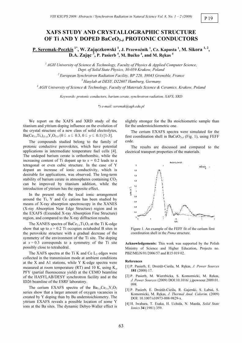
VIII KSUPS 2009: Abstracts / Synchrotron Radiation in Natural Science Vol. 8, No. 1 – 2 (2009)
63
XAFS STUDY AND CRYSTALLOGRAPHIC STRUCTURE
OF Ti AND Y DOPED BaCeO3-δ PROTONIC CONDUCTORS
P. Seremak-Peczkis 1*
, W. Zajączkowski 1, J. Przewoźnik 1, Cz. Kapusta 1, M. Sikora
1, 2,
D.A. Zając 3, P. Pasierb 4, M. Bućko 4, and M. Rękas 4
1 AGH University of Science & Technology, Faculty of Physics & Applied Computer Science,
Dept. of Solid State Physics, 30-059 Krakow, Poland 2 European Synchrotron Radiation Facility, BP 220, 38043 Grenoble, France
3 Hasylab at DESY, D22607 Hamburg, Germany 4 AGH University of Science & Technology, Faculty of Materials Science & Ceramics, Krakow, Poland
Keywords: protonic conductors, barium cerate, synchrotron radiation, XAFS, XRD
*) e-mail: [email protected]
We report on the XAFS and XRD study of the
titanium and yttrium doping influence on the evolution of
the crystal structure of a new class of solid electrolytes,
Ba(Ce1-xTix)(1-y)YyO3-δ (0 ≤ x ≤ 0.3, 0 ≤ y ≤ 0.1) [1-3].
The compounds studied belong to the family of
protonic conductive perovskites, which have potential
applications in intermediate temperature fuel cells [4].
The undoped barium cerate is orthorhombic, while the
increasing content of Ti dopant up to x = 0.2 leads to a
tetragonal or even cubic structure. In the case of Y
dopant an increase of ionic conductivity, which is
desirable for applications, was observed. The long-term
stability of barium cerate in atmospheres containing CO2
can be improved by titanium addition, while the
introduction of yttrium has the opposite effect.
In the present study the local ionic arrangement
around the Ti, Y and Ce cations has been studied by
means of X-ray absorption spectroscopy in the XANES
(X-ray Absorption Near Edge Structure) region and in
the EXAFS (Extended X-ray Absorption Fine Structure)
region, and compared to the X-ray diffraction results.
The XANES spectra of BaCe1-xTixO3 at the Ti K-edge
show that up to x = 0.2 Ti occupies octahedral B sites in
the perovskite structure with a gradual decrease of the
symmetry of the environment of the Ti site. The doping
at x = 0.3 corresponds to a symmetry of the Ti site
possibly close to tetrahedral.
The XAFS spectra at the Ti K and Ce L2 edges were
collected in the transmission mode at ambient conditions
at the X and A1 stations, while Y K-edge spectra were
measured at room temperature (RT) and 10 K, using Kα
PFY (partial fluorescence yield) at the CEMO beamline
of the HASYLAB/DESY synchrotron facility and at the
ID26 beamline of the ESRF laboratory.
The cerium EXAFS spectra of the Ba1-yCe1-xYxO3
series show that a larger amount of oxygen vacancies is
created by Y doping than by Ba understoichiometry. The
yttrium EXAFS reveals a possible location of some Y
ions at the Ba sites. The dynamic Debye-Waller effect is
slightly stronger for the Ba stoichiometric sample than
for the understoichiometric one.
The cerium EXAFS spectra were simulated for the
first coordination shell in BaCeO3-δ (Fig. 1), using FEFF
code.
The results are discussed and compared to the
electrical transport properties of the materials.
Figure 1. An example of the FEFF fit of the cerium first
coordination shell in the Pnma structure.
Acknowledgements: This work was supported by the Polish
Ministry of Science and Higher Education, Projects no.
PBZ/MEiN/01/2006/57 and R15 019 02.
References
[1] P. Pasierb, E. Drożdż-Cieśla, M. Rękas, J. Power Sources
181 (2008) 17.
[2] P. Pasierb, M. Wierzbicka, S. Komornicki, M. Rekas,
J. Power Sources (2009) DOI:10.1016/ j.jpowsour.2009.01.
098.
[3] P. Pasierb, E. Drożdż-Cieśla, R. Gajerski, S. Łabuś, S.
Komornicki, M. Rękas, J. Thermal Anal. Calorim. (2009)
DOI: 10.1007/s10973-008-9829-x.
[4] H. Iwahara, T. Esaka, H. Uchida, N. Maeda, Solid State
Ionics 34 (1981) 359.
P 19

VIII KSUPS 2009: Abstracts / Synchrotron Radiation in Natural Science Vol. 8, No. 1 – 2 (2009)
64
XAFS STUDY OF ZrO2–BASED SOFC MATERIALS
J. Stępień 1*, J. Śliwińska 1, J. Przewoźnik 1, K. Schneider 1, Cz. Kapusta 1, D. Zajac 2, K. Michałów 3, D. Pomykalska 3, M. Bućko 3, and M. Rękas 3
1 AGH University of Science and Technology, Faculty of Physics and Applied Computer Science,
Dept. Solid State Phys., Al. Mickiewicza 30, 30-059 Krakow, Poland 2 Hasylab at DESY, D22607 Hamburg, Germany
3 AGH University of Science and Technology, Faculty of Material Science and Ceramics, Al. Mickiewicza 30, 30-059 Krakow, Poland
Keywords: stabilised zirconia solid solution, synchrotron radiation, XAFS, solid oxide fuel cell
*) e-mail: [email protected]
A XAFS study of yttrium stabilized manganese doped zirconia solid solutions is presented. The materials are promising candidates for intermediate layers between electrolyte and cathode in solid oxide fuel cells. Presence of manganese in the zirconia solid solution is expected to bring about electronic conductivity owing to the formation of electron defects at manganese ions. In consequence, the resistance for charge transfer between electrolyte and cathode would be reduced.
Powder samples of Mnx(Y0.08Zr0.92)1−xO2−δ (0 < x < 0.25) used for XAFS study were prepared by co-precipitation-calcination method and then sintered for 2 h at 1500°C. The dependence of the lattice parameters on x follows the Vegard rule from zero to about 18 mol.% of manganese where the cubic zirconia structure of the solid solution is preserved.
The measurements have been carried out in Hasylab/DESY, Hamburg, in the XANES (X-ray Absorption Near Edge Structure) and EXAFS (Extended X-ray Absorption Fine Structure) ranges at the manganese and yttrium K edges at room temperature and at 10 K. The XANES spectra at the Mn K edge are presented in Fig. 1.
Figure 1. XANES spectra of Mn:K edge of yttrium stabilised zirconia oxide doped with 5, 10 and 15% of manganese.
The absorption edge energies of the samples studied derived from the spectra were compared to those of the reference samples. Assuming a linear dependence between the valence and the edge energy, the valences of Mn in the samples studied were obtained. They are collected in the table below and show that the Mn average oxidation degree is between +2 and +3. It increases with increasing manganese content.
Sample Edge energy [eV] Average oxidation 5% Mn 6547.0 2.44± 0.02 10% Mn 6547.2 2.47± 0,02 15% Mn 6547.7 2.60± 0.02
Fourier transforms of EXAFS spectra obtained at the Y K edge are presented in Fig. 2. They show significant changes with Mn content in the second coordination shell (3.6 Å) corresponding to metal ions, whereas only slight modifications in the first coordination shell (2.1 Å) corresponding to oxygen neighbours is found.
Acknowledgements: This work was supported by the Polish Ministry of Science and Higher Education, Projects no. PBZ/MEiN/01/2006/57 and R15 019 02.
Figure 2. Fourier transforms of the EXAFS spectra obtained at the Y K edge at room temperature for the zirconia oxide doped with 2.5%, 15% and 25% Mn.
P 20

VIII KSUPS 2009: Abstracts / Synchrotron Radiation in Natural Science Vol. 8, No. 1 – 2 (2009)
65
THE SIMULATION OF BRAGG-CASE SECTION IMAGES
OF DISLOCATIONS AND INCLUSIONS IN ASPECT OF IDENTIFICATION
OF DEFECTS IN SiC CRYSTALS
T. Balcer 1*
and W. Wierzchowski 1
1 Institute of Electronic Materials Technology, ul. Wolczynska 131, 01-919 Warsaw, Poland
Keywords: dislocation, rod-like inclusion, micro-pipes, numerical simulation, SiC
Bragg-case section topography is the important
method of X-ray diffraction topography allowing to
reveal fine details of strains defects thanks to appearing
of the interference effects. It also provides the possibility
of effective simulation of the images of topographical
defects based on the numerical integration of the Takagi
equations. The formation of contrast in the method seems
to be equivalent to the diffraction of the spherical wave
from a certain number of closely located excitation
points.
In the present paper the conventional section
topography supported by numerical simulation of defects
is applied for studying of the images of dislocation and
pipe-formed cavities in SiC bulk crystals. The important
goal of the paper was also studying of the elements of the
contrast of the dislocations to check the possibility of
using simple approximations of extinction contrast, often
dominating in the Bragg-case section images of
dislocations.
The numerical analysis of the Bragg-case section
images was performed for the case of screw dislocation
perpendicular to the crystal surface in an arbitrary
asymmetrical reflection. It is well known that this kind of
dislocations is particularly important in the case of SiC,
because it is relatively common and was also suggested
by Dudley and coworkers [1] as the possible source of
micro-pipes, where many single screw dislocations may
join in forming one hollow-core super-screw dislocations
with a large Burgers vector.
The present simulation became more realistic and
better corresponding to the experimental dislocation
images by adding many shifted spherical images, filing
the area irradiated by the narrow beam, analogously at it
was proposed by Epelboin and Soyer [2] in the case of
transmission projection topography. The obtained
simulated images were compared with two adapted
simplified models of extinction contrast described by
Miltat and Bowen [3]. The results evidently indicated
that the extinction contrast in the simulated images and
topographs is very similar to the contours limiting the
effective change of the diffracting conditions and differs
substantially from the contours representing the
condition of the wave-field decomposition.
For studying of the strain field of some pipe-formed
cavities and rod like defects, we revealed a method of
approximate evaluation of the strain field of rod like
inclusion, integrating the contribution from a very large
number of point like inclusions filling the assumed
volume of inclusion. The model allowed taking into
account the relaxation of strains on the free surface using
the initial formulae given by Sen [4], and calculation of
strains for differently inclined rods. The application of
the model enabled obtaining realistic test simulation of
topographic images of some solute trails in garnet, and
some similarity to the Bragg-case section topographic
images of some pipe formed inclusions in SiC.
References
[1] M. Dudley X.R. Huang, V.M. Vetter, "Contribution of x-ray
topography and high-resolution diffraction to the study of
defects in SiC", J. Phys. D: Appl. Phys. 36 (2003) A30–
A36.
[2] Y. Epelboin, A. Soyer, "Simulation of X-ray traverse
topographs by means of a computer", Acta Cryst. A 41
(1985) 67–72.
[3] J.E.A. Miltat, D.K. Bowen, "On the widths of dislocation
images in X-ray topography under low-absorption
conditions", J. Appl. Cryst. 8 (1975) 657–669.
[4] R. Sen, J. Quant. Mech. VIII (4) (1949) 365.
P 21

VIII KSUPS 2009: Abstracts / Synchrotron Radiation in Natural Science Vol. 8, No. 1 – 2 (2009)
66
KINETICS OF THE VERWEY TRANSITION IN MAGNETITE
W. Tabiś 1*, J. Kusz 2, N.-T.H. Kim-Ngan 3, Z. Tarnowski 1, F. Zontone 4, Z. Kąkol 1, A. Kozłowski 1, and T. Kołodziej 1
1 AGH University of Science and Technology, Faculty of Physics and Applied Computer Science,
Al. Mickiewicza 30, 30-059 Kraków, Poland 2 Institute of Physics, University of Silesia, Uniwersytecka 4, 40- 007 Katowice, Poland
3 Institut of Physics, Pedagogical University, Kraków, Poland 4 European Synchrotron Radiation Facility, P.B. 200, F-38043 Grenoble, France
Keywords: magnetite, Verwey phase transition, diffraction
*) e-mail: [email protected]
The Verwey phase transition in magnetite at 124 K is
mainly known due to the drop of resistance by two orders of magnitude while heating above the Verwey temperature TV. Following the concept of Verwey [1] and Anderson [2], it was believed that strongly correlated electrons, one from each of two iron located at octahedral B-sites, travelling relatively freely between iron B cations, are responsible for the good conductivity at T > TV. The abrupt increase in resistivity below TV was explained as due to the localization of those interacting electrons at particular positions. The low-temperature order is described by formula: Fe3+ [Fe(2.5+δ)+ Fe(2.5-δ)+] O4 where the square brackets mark the octahedral positions. The disproportionation value of δ12 = 0.12 ± 0.025 for one kind of Fe-atoms and δ34 = 0.1 ± 0.06 for another is confirmed by a resonant x-ray diffraction (RXD) [3]. This electronic charge ordering is related to the change in the structure symmetry, from high T cubic (Fd-3m) to monoclinic (Cc) for T below TV. The results of recent investigations, however, suggest that there is decoupling between charge ordering and the lattice distortion [4].
To investigate the kinetics of the transition in details, two kinds of experiments has been performed. First, simultaneous measurements of the resistivity and the magnetic susceptibility while temperature maintained constant, were performed at the AGH Univ. of Sci. and Tech. in Krakow. The results are shown in Fig. 1.
The second experiment has been performed at ESRF in Grenoble, ID10 beam line. The aim was to work out the processes related to the lattice distortion. For that we observed simultaneously the (1 1½ 2) superstructure peak intensity (absent in high-T cubic phase) and, for comparison with the previous experiment, the magnetic susceptibility. The results are shown in Fig. 2.
We have traced all the ongoing processes, trying to see their temporal dependences and the subtleties of the transition. We note here that, although AC susceptibility is a magnetic parameter, it reflects booth the changing electronic system and the structure symmetry.
Acknowledgements: The project was supported by the Polish Ministry of Education and Science grant No 1P03 B01530. References
[1] E.J. Verwey, "Electronic conduction of magnetite (Fe3O4) and its transition point at low temperatures". Nature (London) 144 (1939) 327–328.
[2] P.W. Anderson, "Ordering and antiferromagnetism in ferrites", Phys. Rev. 102 (1956) 1008–1013.
[3] E. Nazarenko, et al., "Resonant x-ray diffraction studies on the charge ordering in magnetite", Phys. Rev. Lett. 97 (2006) 056403–1–4.
[4] J.E. Lorenzo, et al., "Charge and orbital correlations at and above Verwey phase transition in magnetite", Phys. Rev. Let. 101 (2008) 226401–1–4.
Figure 1. Temporal behavior of the resistivity R(t) and the magnetic AC susceptibility χAC(t) measured simultaneously with the temperature T(t) at the Verwey transition during sample cooling.
Figure 2. Temporal behavior of the integrated (1 3/2 2) superstructure peak intensity I(t) and the magnetic AC susceptibility χAC(t) measured simultaneously with the temperature T(t) at the Verwey transition.
P 22

VIII KSUPS 2009: Abstracts / Synchrotron Radiation in Natural Science Vol. 8, No. 1 – 2 (2009)
67
CHANGES OF IRON STATE AND LOCAL IRON ENVIRONMENT OF MALARIAL PIGMENT'S SUBSTITUTE IN PRESENCE
OF CHLOROQUINE
M.S. Walczak 1*, K. Lawniczak-Jablonska 1, A. Wolska 1, M. Sikora 2,3, A. Sienkiewicz 4, L. Suárez 5, A. Kosar 5, M.J. Bellemare 5, and D.S. Bohle 5
1 Institute of Physics, PAS, Al. Lotników 32/46, 02-668 Warsaw, Poland
2 Faculty of Physics and Applied Computer Science, AGH University of Science and Technology, Al. Mickiewicza 30, 30-059 Krakow, Poland
3 European Synchrotron Radiation Facility, BP 220, 38043 Grenoble, France 4 Institute of Physics of Condensed Matter, Ecole Polytechnique Fédérale de Lausanne,
CH-1015 Lausanne, Switzerland 5 Department of Chemistry, McGill University, 801 Sherbrooke Street West, Montreal, Canada
Keywords: hemozoin, hemozoin's substitute, chloroquine, EXAFS, XANES
*) e-mail: [email protected]
Malaria remains the world’s most prevalent vector-
borne disease, which causes serious health problem particularly in African and Asiatic countries [1]. The most severe form of malaria is caused by Plasmodium falciparum (Pf) parasite. The intraerythrocytic stage of Pf involves hemoglobin proteolysis and detoxification of heme molecules into an inert crystalline material, called malarial pigment, or hemozoin. The crystal structure of hemozoin has been solved by X-ray powder diffraction in the last years and its synthetic analogue, β-hematin was synthesized [2]. The ferriprotoporphyrin IX is believed to be a target for commonly used antimalarial drugs but their interactions are still not understood on molecular level.
In presented work we are especially interested in drug-induced perturbations of the structures of soluble β-hematin-like compound, iron(III) (meso-porphyrin-IX anhydride) called meso-hematin. Similarly to its insoluble parent compound, β-hematin, this compound is also built of dimers. The XAS measurements on frozen sample of meso-hematin in solution were performed at ESRF (station ID26). Pure acetic acid and acetic acid with water of volume ratio respectively 30:1 and 15:1 were used as solvents. The high resolution XANES and EXAFS spectra on iron K-edge enabled us to reveal the evolution of iron oxidation state and local environment of Fe atoms in investigated solutions upon chloroquine drug addition. The main difference revealed by EXAFS concerns the coordination number of the ligand oxygen, which is lower in the presence of chloroquine for both the water containing solutions. On the other hand the Fe-O distance is significantly shorter in solution with smaller H2O/acetic acid ratio and at the presence of drug. Analysis of the XANES revealed small changes in local iron geometry and its spin state, being close to S = 3/2, instead of S = 5/2 observed in natural product of malaria parasite – microcrystalline hemozoin. Acknowledgements: This work was supported by research grant N20205332/1197 and special project ESRF/73/2006 from the Ministry of Science and High Education.
References
[1] (a) L.H. Miller, D.I. Baruch, K. Marsch, O.K. Duombo, "The pathogenic basis of malaria", Nature 415 (2002) 673-679; (b) World Health Organization, The World Malaria Report 2008, http://apps.who.int/malaria/wmr2008/
[2] S. Pagola, P.W. Stephens, D.S. Bohle, A.D. Kosar, S.K. Madsen, "The structure of malaria pigment beta-haematin", Nature 404 (2000) 307-310.
0
10
20
30
40
50
1 2 3 4 5 6
FT
k3 *χ
(k)
r [A]
MDAA15
0
10
20
30
40
50
1 2 3 4 5 6
FT
k3 *χ
(k)
r [A]
MDAA30
0
10
20
30
40
50
1 2 3 4 5 6
FT
k3 *χ
(k)
r [A]
MDAA
Figure 1. Comparison of Fourier transformed EXAFS oscillationsof solved meso-hematin without (MDAA) and with (MDAA15, MDAA30) water addition.
0
10
20
30
40
50
1 2 3 4 5 6
FT
k3 *χ
(k)
r [A]
MDAAQ15
0
10
20
30
40
50
1 2 3 4 5 6
FT
k3 *χ
(k)
r [A]
MDAAQ30
0
10
20
30
40
50
1 2 3 4 5 6
FT
k3 *χ
(k)
r [A]
MDAAQ
Figure 2. Comparison of Fourier transformed EXAFS oscillations of solved meso-hematin in chloroquine presence without (MDAAQ) and with (MDAAQ15, MDAAQ30) water addition.
P 23

VIII KSUPS 2009: Abstracts / Synchrotron Radiation in Natural Science Vol. 8, No. 1 – 2 (2009)
68
HIGH-PRESSURE DIFFRACTION STUDY OF SELECTED SYNTHETIC GARNETS
E. Werner-Malento 1*, R. Minikayev 1, C. Lathe 2, 3, H. Dąbkowska 4, and W. Paszkowicz 1
1 Institute of Physics, Polish Academy of Sciences, Al. Lotników 32/46, 02-668 Warsaw, Poland
2 HASYLAB at DESY, Notkestrasse 85, D-22603 Hamburg, Germany 3 GFZ German Research Centre for Geosciences, Dept. 5, Telegraphenberg, Potsdam, Brb D-14473, Germany
4 Department of Physics, McMaster University, Hamilton, Ontario, L8S 4M1 Canada
Keywords: garnets, equation of state, EOS, high-pressure diffraction study
*) e-mail: [email protected]
Crystals of synthetic garnets exhibit physical properties that may lead to various appilcations. These materials are characterized by high resistance for plastic flow even at high temperatures, by low thermal conductivity [1], and by Mohs hardness between 6.5 and 8.5. Garnets are applied in solid-state lasers [2]. Some of them (e.g. Gd3Ga5O12, gadolinium gallium garnet – GGG) can be used for substrates for epitaxy of superconducting films [3]. Some doped oxide garnet materials can be used as optical pressure sensors [4, 5].
Mechanical properties of garnets are also of interest from the point of view of Earth science, because minerals of garnet structure are considered as one of major componets of the deep interior of the Earth [6].
The general chemical formula for a garnet is X3Y2Z3O12, with divalent X, trivalent Y, and tetravalent Z cations (for exampple: Ca3Ga2Ge3O12) or with trivalent cations.
At ambient conditions, garnets crystallize in Ia3d space group. In four-component’s garnets (X3Y2Z3O12), the Z atoms are bonded to four oxygens (tetrahedral), Y atoms – to six oxygens (octahedral), and X atoms – to eight oxygens (distorted cube). In three-component garnets (X3Y5O12) the five Y ions occupy two octahedral and three tetrahedral sites.
High-pressure diffraction study for selected garnets is presented in this work. The in-situ X-ray diffraction experiments were conducted using the energy-dispersive method at the F2.1 beamline equipped with a large-anvil diffraction press, MAX80. The pressures ranging to 8.7 GPa were calibrated using a NaCl equation of state. The lattice parameters of garnets were determined from Le Bail refinements performed with the Fullprof2k program.
Analysis of the data collected for one of the measured garnets, Ca3Ga2Ge3O12 (calcium gallium germanium garnet, CGGG) shows that the garnet structure is conserved in the studied pressure range. The lattice parameter of the garnet structure decreases with the applied pressure from 12.202(1) Å at ambient pressure to 11.995(4) Å at 8.7 GPa. The resulting bulk modulus value for the CGGG is by about 15% lower than that for gadolinium gallium garnet [7].
30 40 50 60 70
-10000
-5000
0
5000
10000
15000
20000
25000
30000
35000
Inte
nsity
Energy [keV]
Observed pattern Bragg positions Calculated pattern Diffrence pattern
CGGGhBN
Figure 1. Le Bail refinement plot of the calcium gallium germanium garnet, sample after compression without pressure. The vertical bars refer to peak positions for CGGG and hBN.
References
[1] N.P. Padture, P.G. Klemens, "Low thermal conductivity in garnets", J. Am. Ceram. Soc. 80 (1996) 1018–1020.
[2] J. Lu, K. Ueda, H. Yagi, T. Yanagitani, Y. Akiyama, A.A. Kaminskii, "Neodymium doped yttrium aluminum garnet (Y3Al5O12) nanocrystalline ceramics—a new generation of solid state laser and optical materiale", J. Alloys Compds. 341 (2002) 220–225.
[3] P. Mukhopadhyay, "High-Tc films on GGG substrates", Supercond. Sci. Technol. 7 (1993) 298–299.
[4] J. Liu, Y.K. Vohra, "Sm:YAG optical pressure sensor to 180 GPa: Calibration and structural disorder", Appl. Phys. Lett. 64 (1994) 3386–3388.
[5] S. Kobyakov, A. Kamiska, A. Suchocki, D. Galanciak, M. Malinowski, "Nd3+-doped yttrium aluminum garnet crystal as a near-infrared pressure sensor for diamond anvil cells", Appl. Phys. Lett. 88 (2006) 234102.
[6] S. Karato, Z. Wang, B. Liu, K. Fujino, "Plastic deformation of garnets: systematics and implications for the rheology of the mantle transition zone", Earth Planet. Sci. Lett. 130 (1995) 13–30.
[7] A. Durygin, V. Drozd, W. Paszkowicz, E. Werner-Malento, R. Buczko, A. Kaminska, S. Saxena, A. Suchocki, "Influence of pressure on lattice parameter of gadolinium gallium garnet crystals", Appl. Phys. Lett. (2009), accepted.
P 24

VIII KSUPS 2009: Abstracts / Synchrotron Radiation in Natural Science Vol. 8, No. 1 – 2 (2009)
DAMAGE OF SOLIDS INDUCED BY SINGLE PULSES OF XUV-FLASH
J.B. Pełka 1, R. Sobierajski 1 , M. Jurek 1, J. Krzywiński 1, D. Żymierska 1, D. Klinger 1,S. Hau Riege 2, H. Chapman 2, R. London 2, L. Juha 3, J. Chalupsky 3, J. Cihelka 3,
U. Jastrow 4, K. Tiedtke 4, S. Toleikis 4, H. Wabnitz 4, W. Caliebe 4, K. Sokolowski-Tinten 5,N. Stojanovic 5, C. Riekel 6, R. Davies 6, M. Burghammer 6, W. Paszkowicz 1, and A. Wawro 1
1 Institute of Physics, Polish Academy of Sciences, Al. Lotnikow 32/46, 02-668 Warsaw, Poland2 Lawrence Livermore National Laboratory, 7000 East Avenue, Livermore, CA 9455, USA
3 Institute of Physics, Academy of Sciences of the Czech Republic, Na Slovance 2, 182 21 Prague, Czech Republic4 Deutsches Elektronen-Synchrotron DESY, Notkestrasse 85, D-226 3 Hamburg, Germany
5 Institut für Experimentelle Physik, Universität Duisburg-Essen, Lotharstr. 1, 4748 Duisburg, Germany6 European Synchrotron Radiation Facility, 6 rue Jules Horowitz, BP 220, 38043 Grenoble, France
Keywords: XUV FEL, radiation damage, ablation, structure modifications, x-ray diffraction,pump and probes
*) e-mail: [email protected]
The VUV- and XUV-FEL beam interaction with
matter has been extensively investigated for the last few
years with a special attention paid to the damage induced
in solids. Most of this work was performed with the Free
electron LASer in Hamburg (FLASH). This new type of
the IVth generation SR source delivers intense pulses of
coherent light in the wavelength range of 6 - 50 nm with
the unique combination of quantum energy, extreme short
pulse duration of only 25 fs and high power/pulse up to 5
GW. Application of the radiation opens up an access to
study not yet explored phenomena, remaining
unattainable with classical sources.
Interaction of XUV FLASH pulses with solids can
change optical properties of the materials and induces
complex damage processes leading to the formation of
specific morphological structures with sizes on
micrometric and nanometric scales [1, 2]. The absorbed
pulse energy can also provoke phase transitions that
change composition or crystalline state of the near-surface
material [3]. Investigation of these phenomena is crucial
for refinement of theoretical models, necessary to predict
performance and lifetime of optical components for the
new generation of FELs operating in the XUV and X-ray
region.
In this work we put together some of our important
experimental results, obtained with aid of various
techniques, on the interaction of high intensity (1011 –1014
W/cm2) ultrashort pulses, delivered by FLASH, with
solids. The one-color pump and probe technique made it
possible to probe fluency-dependent variations in the
optical constants of materials on the time scales of a
single pulse duration.
The dynamics of ablation process was studied on the
sample surface by the two-color pump and probe method
with aid of an external optical laser. A detailed ex-situ
characterization of irradiation-induced modifications on
the solid surfaces was obtained by mixing the traditional
microscopic methods with AFM. The x-ray
microdiffraction with submicrometer beam was applied to
probe the crystalline state with lateral resolution of only
250 nm.
By combining the results obtained with various
experimental techniques, a more comprehensive picture
of the processes in solids excited by an intense
femtosecond XUV pulse was achieved.
Acknowledgements: This work has been partially supported by
the Ministry of Science and Higher Education of Poland, SPB
nr. DESY/68/2007, by the Czech Ministry of Education from the
National Research Centers program (Projects LC510 and
LC528) and program INGO (Grant LA08024) and by Academy
of Sciences of the Czech Republic (Grants Z10100523,
IAA400100701, and KAN300100702). Irradiation with FLASH
has been performed within the framework of the Peak-
Brightness-Collaboration [project II-20022049 EC]. Support
from the PBC and the operators of the FLASH facility are
gratefully acknowledged. The synchrotron measurements at
HASYLAB, Hamburg were supported by the RIA FP6 Contract
RII3-CT-2004-506008 of the European Community, The
microdiffraction study has been done at the ID-13 beamline at
ESRF, Grenoble.
References
[1] S.P. Hau-Riege, R.A. London, R.M. Bionta, M.A.
McKernan, S.L. Baker, J. Krzywinski, R. Sobierajski, R.
Nietubyc, J.B. Pelka, M. Jurek, L. Juha, J. Chalupský, J.
Cihelka, V. Hájková, A. Velyhan, J. Krása, "Damage
threshold of inorganic solids under free-electron-laser
irradiation at 32.5 nm wavelength", Appl. Phys. Lett. 90
(2007) 173128.
[2] J. Krzywinski, R. Sobierajski, M. Jurek, R. Nietubyc, J.
Pelka, L. Juha, M. Bittner, V. Létal, V. Vorlíček, A.
Andrejczuk, J. Feldhaus, B. Keitel, E.L. Saldin, E.A.
Schneidmiller, R. Treusch, M.V. Yurkov, "Conductors,
semiconductors, and insulators irradiated with short-
wavelength free-electron laser", J. Appl. Phys. 101 (2007)
043107.
[3] J.B. Pelka, R. Sobierajski, D. Klinger, W. Paszkowicz,, J.
Krzywinski, M. Jurek, D. Zymierska, A. Wawro, A.
Petroutchik, L. Juha, V. Hajkova, J. Cihelka, J. Chalupsky, T.
Burian, L. Vysin, S. Toleikis, K. Sokolowski-Tinten, N.
Stojanovic, U. Zastrau, R. London, S. Hau-Riege, C. Riekel,
R. Davies, M. Burghammer, E. Dynowska, W.
Szuszkiewicz, W. Caliebe, R. Nietubyc, "Damage in solids
irradiated by a single shot of XUV free-electron laser:
Irreversible changes investigated using X-ray
microdiffraction, atomic force microscopy and Nomarski
optical microscopy, "Rad. Phys. Chem. 78, (2009) S46-S52.
69
P 25
VIII KSUPS 2009: Abstracts / Synchrotron Radiation in Natural Science Vol. 8, No. 1 – 2 (2009)
70
ALIGNMENT TEST OF N-DOPED CARBON NANOTUBES
USING HIGH-ENERGY X-RAY DIFFRACION
L. Hawelek 1, A. Brodka
1, J.C. Dore
2, V. Honkimäki
3, T. Kyotani
4, and A. Burian
1
1 A. Chelkowski Institute of Physics, University of Silesia,
ul. Uniwersytecka 4, 40-007 Katowice, Poland 2 School of Physical Sciences, University of Kent, Canterbury, CT2 7NR, UK
3 European Synchrotron Radiation Facility, BP 220, 38043 Grenoble, France 4 Institute of Multidisciplinary Research and Advanced Material, Tohoku University,
Katahira, Sendai 980-88577 Japan
Keywords: N-doped carbon nanotubes; X-ray diffraction
Alignment test of multi-wall N-doped carbon
nanotubes prepared by template pyrolytic carbon
deposition method inside channels of an alumina
membrane have been performed using high-energy X-ray
diffraction on the ID15B beam-line at the European
Synchrotron Radiation Facility (ESRF, Grenoble). The
two-dimensional diffraction pattern of deposited carbon
nanotubes, recorded directly within the alumina
membrane using image plate detector, exhibits two non-
continues arcs corresponding to the (002) graphitic
reflection. Four values of angle between the axis of
carbon nanotubes within membrane channels and the
incident beam were taken into consideration (0, 30, 45
and 60 degree). The anisotropic scattering distribution of
two-dimensional pattern corresponds to the appropriate
position of the carbon nanotubes, thus indicates their
alignments. The one-dimensional intensity pattern for
(002) anisotropic peaks over whole azimuthal angle was
performed by circular slicing the two-dimensional
pattern and the Full Width at Half Maximum (FWHM)
parameter of anisotropy effect was determined by
procedure of non-linear Gaussian curve fitting.
P 26

VIII KSUPS 2009: Abstracts / Synchrotron Radiation in Natural Science Vol. 8, No. 1 – 2 (2009)
71
OKREŚLANIE LOKALNEGO OTOCZENIA WOKÓŁ WYBRANYCH
ATOMÓW W NOWYCH WODORKACH FAZ LAVESA
K. Lawniczak-Jablonska 1*
, M.T. Klepka 1, A. Wolska
1, S. Filipek
2, and R. Sato
2
1 Instytut Fizyki PAN, al. Lotników 32/46, 02-668 Warszawa, Polska
2 Instytut Chemii Fizycznej PAN, ul. Kasprzaka 44/52, 01 224 Warszawa, Polska
Słowa kluczowe: fazy Laves'a, absorpcja rentgenowska, wiązanie chemiczne
*) e-mail: [email protected]
Absorpcja rentgenowska jest unikatową techniką,
która pozwala wyznaczyć położenie atomów danego
pierwiastka w sieci krystalicznej, określić jego wiązanie
chemiczne oraz zmiany wprowadzone poprzez różnego
rodzaju procedury (np. wygrzewanie, wprowadzenie
wodoru, czy domieszkowanie). Technika ta jest więc
doskonałym narzędziem do badania nowych materiałów.
W niniejszej pracy zastosowano tą metodę do badania
nowych wodorków faz Lavesa.
Fazy Lavesa są grupą międzymetalicznych
związków, które poza bardzo interesującymi
własnościami fizycznymi i chemicznymi są uważane za
ważne materiały w kontekście poszukiwania nośników
wodoru dla energetyki wodorowej, w której wodór
miałby zastąpić konwencjonalne źródła energii.
Zainteresowanie nimi związane jest więc również z
rozwojem energetyki wodorowej. Udało się ostatnio
zsyntezować stosując technikę wysokich ciśnień szereg
nowych wodorków faz Lavesa. Wodorki te są stabilne i
mogą być przechowywane przez długi czas w warunkach
normalnego ciśnienia i temperatury [1]. Pośród nowo
zsyntezowanych materiałów najbardziej interesująca
wydaje się grupa deuterków opisana wzorem
chemicznym RMn2D6 (gdzie R = Y lub Dy oraz
pseudobinarne związki, w których Mn jest częściowo
zastąpiony przez Fe lub Cr). Materiały takie udało się po
raz pierwszy wytworzy ze związków Lavesa. Ich
własności fizyczne i chemiczne są intensywnie badane,
ale położenie atomów Fe i Cr w sieci krystalicznej nie
zostało do tej pory jednoznacznie wyznaczone [2].
Pomiary krawędzi absorpcji K Mn, Fe i Cr
przeprowadzono w HASYLAB na stacji E4 w zakresie
bliskim krawędzi (XANES z ang. X-ray Absorption Near
Edge Structure) i dla rozciągłej struktury (EXAFS z ang.
Extended X-ray Absorption Fine Structure). W celu
dokonania analizy tych widm przeprowadzono obliczenia
widma XANES dla różnych położeń atomów Mn, Fe i Cr
w sieci krystalicznej tych związków korzystając z
programu FEFF8.4. Widma teoretyczne zostały następnie
porównane z widmami eksperymentalnymi. Pozwoliło to
stwierdzić, który z modeli jest najbliższy rzeczywistemu
rozmieszczeniu atomów w sieci. Rozważono również
możliwość występowania danego pierwiastka w więcej
niż jednym położeniu w sieci.
Do analizy widm EXAFS zastosowano programy
Artemis i Athena z pakietu IFEFIT. Związki podwójne
były wykorzystane jako materiały referencyjne o znanej
strukturze. Określono zmiany w wiązaniu chemicznym
wprowadzone przez obecność wodoru lub deuteru w
strukturze faz Lavesa oraz wpływ drugiego metalu
przejściowego o dobrze zlokalizowanych stanach d (tutaj
Fe lub Cr). Wyznaczono również położenie atomów Mn,
Fe i Cr w sieci krystalicznej tych materiałów. Pozwoliło
to zweryfikować istniejące modele teoretyczne oraz
wnioski z neutronowych i rentgenowskich badań
dyfrakcyjnych [3]. Po wyznaczeniu właściwego
położenia metali przejściowych w sieci krystalicznej tych
materiałów obliczono strukturę elektronową wokół
każdego z metali i przedyskutowano ją w kontekście
własności fizyko-chemicznych.
Podziękowania: Badania zostały dofinansowane jako wspólne
badania sieci naukowej "Nowe Materiały - wytwarzanie i
badania strukturalne" przez MNiSW oraz z programu Unii
Europejskiej w ramach projektu RII3-CT-2004-506008 (IA-
SFS).
Literatura
[1] V. Paul-Boncour, S.M. Filipek, M. Dorogova, F. Bourée, G.
André, I. Marchuk, A. Percheron-Guégan, R.S. Liu,
"Neutron diffraction study, magnetic properties and thermal
stability of YMn2D6 synthesized under high deuterium
pressure", J. Sol. State Chem. 178 (2005) 356–362.
[2] S.M. Filipek, H. Sugiura, V. Paul-Boncour, R. Wierzbicki,
R.S. Liu, N. Bagkar, "Studies of Novel Deuterides RMn2D6
(R – Rare Earth) compressed in DAC up to 30 GPa", J.
Phys.: Conf. Ser. 121 (2008) 022001.
[3] V. Paul-Boncour, S.M. Filipek, I. Marchuk, G. André, F.
Bourée, G. Wiesinger, A. Percheron-Guégan, "Structural
and magnetic properties of ErFe2D5 studied by neutron
diffraction and Mössbauer spectroscopy", J. Phys.: Cond.
Matt. 15 (2003) 4349–4359.
P 27
VIII KSUPS 2009: Abstracts / Synchrotron Radiation in Natural Science Vol. 8, No. 1 – 2 (2009)
EQUATION OF STATE OF ZIRCON-TYPE TbVO4
R. Minikayev 1, W. Paszkowicz 1, E. Werner-Malento 1, C. Lathe 2,3, and H. Dąbkowska 4
1 Institute of Physics, Polish Academy of Sciences, Al. Lotników 32/46, 02-668 Warsaw, Poland2 HASYLAB at DESY, Notkestrasse 85, D-22603 Hamburg, Germany
3 GFZ German Research Centre for Geosciences, Dept. 5, Telegraphenberg, Potsdam, Brb D-14473, Germany4 Department of Physics, McMaster University, Hamilton, Ontario, L8S 4M1 Canada
Keywords: diffraction, equation of state, orthovanadate, TbVO4, bulk modulus
*) e-mail: [email protected]
RVO4 (R = Y, Sc, La − Lu) orthovanadates belong to
a large class of AXO4 compounds that typically adopt the
structures of zircon, scheelite, fergusonite, monazite,
wolframite, CrVO4, ZnSO4 and rutile types [1-3]. Phase
relationships in this class, observed as a function of
pressure have been systematized by Fukunaga and
Yamaoka [2] and Errandonea and Manjón [4] (for all
possible AXO4 compounds), and by Kolitsch and
Holtstam [3] for RXO4 compounds (X = P, As, V). For
RVO4, R = Pr to Lu, the most stable ambient pressure
structure is of zircon type, space group I41/amd, this
structure can be also obtained for R = La using special
preparation methods. The zircon-type RVO4
orthovanadates exhibit physical properties that may lead
to a number of applications. Known examples are the
europium and neodymium doped YVO4 crystals used as
phospor and laser materials, respectively. Some of
compounds of this family are considered as being
suitable for optical waveguides and polarizers, they can
be used for remote thermometry, as catalysts for
oxidative dehydrogenation, and are candidates for
advanced bio-imaging phosphors and as components of
toughened ceramic composites.
A number of RVO4 oxides have been studied at high-
pressure conditions using the in-situ or ex situ X-ray
diffraction and other methods. They are known to
undergo an irreversible phase transition to scheelite-type
structure. In this work, TbVO4 is studied in the pressure
range 0-7 GPa. The elastic properties of this oxide have
been studied under pressure by an indirect technique,
only, using the Raman spectroscopic data by Chen et
al. [4]. The crystal investigated in the present work was
grown from PbO/PbF2 flux by the slow cooling method.
The in-situ X-ray diffraction experiments were
conducted using the energy-dispersive method at the
F2.1 beamline equipped with a large-anvil diffraction
press,
MAX80. The pressure was calibrated using a NaCl
equation of state. The lattice parameters of TbVO4 were
determined from Le Bail refinements performed with the
Fullprof program. The bulk modulus calculated by fitting
the second order Birch-Murnaghan equation of state to
the unit-cell-volume dependence of pressure. The bulk
modulus value, lattice parameter and axial ratio
dependence on pressure will be shown.
References
[1] O. Muller, R. Roy, "Phase transitions among the ABX4
compounds", Z. Kristallogr. 198 (1973) 237-253.
[2] O. Fukunaga, S. Yamaoka, "Phase transformations in AB04
type compounds under high pressure", Phys. Chem. Miner.
5 (1979) 167-177.
[3] U. Kolitsch, D. Holtstam, "Crystal chemistry of REEXO4
compounds (X = P, As, V). II. Review of REEXO4
compounds and their stability fields", Eur. J. Mineral. 16
(2004) 117-126.
[4] D. Errandonea, F.J. Manjón, "Pressure effects on the
structural and electronic properties of ABX4 scintillating
crystals", Prog. Mater. Sci. 53 (2008) 711.
72
P 28

VIII KSUPS 2009: Abstracts / Synchrotron Radiation in Natural Science Vol. 8, No. 1 – 2 (2009)
73
A COMBINED X-RAY DIFFRACTION AND ABSORPTION STUDY
OF Li2Si2O5 DOPED WITH VANADIUM
W. Paszkowicz 1, A. Wolska
1, M.T. Klepka
1, S. abd el All
1,2, and F.M. Ezz-Eldin
2
1 Institute of Physics PAS, al. Lotników 32/46, Warszawa 02-668, Poland
2 Center of Research and Radiation Technology, Nasr City, Cairo 0002, Egypt
Keywords: X-ray diffraction, X-ray absorption, XANES, lithium silicate
*) e-mail: [email protected]
Lithium-based conducting glasses are promising
candidates for electrolyte materials of thin-film batteries
because they exhibit isotropic ionic conductivity.
However, at room temperature most of such conducting
glasses exhibit relatively low ionic conductivity values,
in the range 10-7 to 10-8 S/m. In order to increase the
conductivity, some specific additives have been used,
one of them being vanadium. In a recent work on borate
glasses, vanadium dopant at a level of several percent
was used for this purpose [1-3]. It has been noticed that
annealing of vanadium doped borate glass results in a
change of physical properties [1]. This may suggest that
vanadium ions occupy specific crystallographic sites.
In this work, a related material, vanadium-doped
lithium silicate glass is studied. The glass was prepared
by heating a mixture of quartz (SiO2), lithium carbonate
(Li2CO3) and vanadium pentoxide (V2O5) at a level of up
to 5.5 weight percent at 1400 for 3 h and then cooled. As
prepared glass was annealed for 4 h at 550°C. The X-ray
diffraction experiments were performed at a conventional
diffractometer.
The described synthesis procedure gives a virtually
pure Li2Si2O5 phase of orthorhombic Ccc2 space group
[4] with vanadium present in the lattice and with traces
of impurity phases. We noticed that the observed
crystallisation is faster than that reported in literature for
phosphate glasses [5]. Rietveld refinements were
performed using various models assuming a partial
occupation at Li or Si sites. The results indicate that
location of vanadium at Si sites is more likely. The lattice
parameters are found to vary isotropically with
increasing vanadium content.
The X-ray absorption experiment was conducted at
the Cemo beamline (Hasylab, Hamburg). XANES
spectra at the vanadium K edge were measured at room
temperature using fluorescence and transmission
detection mode. In all cases, a very pronounced pre-pik
was observed. According to Ref. [6], this feature
indicates that vanadium atoms are in the +5 ionic state.
References
[1] N.A. El-Alaily, R.M. Mohamed, "Effect of irradiation on
differenial thermal properties and crystallization behavior
of some lithium borate glasses", Nucl. Instrum. Meth. Phys.
Res. B 179 (2001) 230-242.
[2] Y.-I. Lee, J.-H. Lee, S.-H. Hong, Y. Park, "Li-ion
conductivity in Li2O–B2O3–V2O5 glass system", Solid State
Ionics 175 (2004) 687–690.
[3] S.Y. Marzouk, N.A. Elalaily, F.M. Ezz-Eldin, W.M. Abd-
Allah, "Optical absorption of gamma-irradiated lithium-
borate glasses doped with different transition metal oxides",
Physica B 382 (2006) 340–351.
[4] B.H.W.S. de Jong, H.T.J. Supér, A.L. Spek, N. Veldman, G.
Nachtegaal, J.C. Fischer, "Mixed alkali systems: Structure
and 29Si MASNMR of Li2Si2O5 and K2Si2O5", Acta
Crystallogr. B 54 (1998) 568-577.
[5] Y. Iqbal, W.E. Lee, D. Holland, P.F. James, "Crystal
nucleation in P2O5-doped lithium disilicate glasses", J.
Mater. Sci. 34 (1999) 4399–4411.
[6] P. Chaurand, J. Rose, V.Briois, M. Salome, O. Proux, V.
Nassif, L. Olivi, J. Susini, J.-L. Hazemann, J.-Y. Bottero
"New methodological approach for the vanadium K-edge
X-ray absorption near-edge structure interpretation:
Application to the speciation of vanadium in oxide phases
from steel slag", J. Phys. Chem. B 111 (2007) 5101-5110.
P 29

VIII KSUPS 2009: Abstracts / Synchrotron Radiation in Natural Science Vol. 8, No. 1 – 2 (2009)
74
LATTICE PARAMETER OF POLYCRYSTALLINE DIAMOND
IN THE LOW-TEMPERATURE RANGE
W. Paszkowicz 1, P. Piszora
2, W. Łasocha
3,4, I. Margiolaki
5, M. Brunelli
5, and A. Fitch
5
1 Institute of Physics PAS, al. Lotników 32/46, 02-668 Warszawa, Poland
2 Adam Mickiewicz University, Faculty of Chemistry,
ul. Grunwaldzka 6, Poznań 60-780, Poland 3 Jagellonian University, Faculty of Chemistry, ul. Ingardena 3, 30-060 Kraków, Poland
4 Institute of Catalysis and Surface Chemistry PAS,
ul. Niezapominajek 8, 30-239 Kraków, Poland 5 European Synchrotron Radiation Facility (ESRF), ID31, Materials Science Group, Inorganic Chemistry I,
6 rue Jules Horowitz, BP 220, 38043 Grenoble, France
Keywords: thermal expansion, X-ray diffraction, diamond
*) e-mail: [email protected]
Diamond exhibits, due to strong covalent bonding, a very weak thermal expansion at low temperatures. Below room temperature, the total variation of the unit-cell dimension is less than 10-3 Å, being comparable to the precision of lattice-parameter determination at a typical instrument. Experimental studies have been published for diamond single crystals [1, 2], whereas detailed experimental studies for polycrystalline diamond have been reported mainly above the room temperature.
In the present study, the results of measurement of lattice parameters of commercial polycrystalline diamond will be presented. The measurements were performed using Debye-Scherrer geometry at ID31 beamline (ESRF) equipped with a bank of nine detectors preceded by Si 111 analyser crystals. Lattice parameters were calculated using the Rietveld refinement. The obtained
experimental lattice parameter and thermal expansion temperature dependence will be discussed on the basis of available literature data.
References
[1] T. Saotome, K. Ohashi, T. Sato, H. Maeta, K. Haruna, F.
Ono, "Thermal expansion of a boron-doped diamond single
crystal at low temperatures", J. Phys.: Condens. Matt. 10
(1998) 1267–1272.
[2] T. Sato, K. Ohashi, T. Sudoh, K. Haruna, H. Maeta,
"Thermal expansion of a high purity synthetic diamond
single crystal at low temperatures", Phys. Rev. B 65 (2002)
092102.
[3] C. Giles, C. Adriano, A. Freire Lubambo, C. Cusatis, I.
Mazzaro, M. Goncalves Hönnicke, "Diamond thermal
expansion measurement using transmitted X-ray back-
diffraction", J. Synchrotron Radiat. 12 (2005) 349–353.
P 30

VIII KSUPS 2009: Extended abstracts / Synchrotron Radiation in Natural Science Vol. 8, No. 1 – 2 (2009)
75
A COMPARISON OF THE VALENCE BAND STRUCTURE
OF BULK AND EPITAXIAL GeTe-BASED
DILUTED MAGNETIC SEMICONDUCTORS
M.A. Pietrzyk 1*, B.J. Kowalski
1, B.A. Orlowski
1, W. Knoff
1, T. Story
1, W. Dobrowolski
1,
V.E. Slynko 2, E.I. Slynko
2, and R.L. Johnson
3
1
Institute of Physics, Polish Academy of Sciences, Al. Lotnikow 32/46, 02-668 Warsaw, Poland 2 Chernivtsi Branch of the Institute for Materials Science Problems, National Academy of Sciences of Ukraine,
5 Vilde Str., 58001 Chernivtsi, Ukraine 3 Institute of Experimental Physics, University of Hamburg, Luruper Chaussee 149, D-22761 Hamburg, Germany
Keywords: photoemission spectroscopy, diluted magnetic semiconductors
*) e-mail: [email protected]
In this work we present a comparison of the
experimental results, which have been obtained in the
resonant photoemission study of electronic structure of
epitaxial layers and bulk crystals of GeTe doped with Mn
and/or Eu. Narrow-gap IV–VI semiconductors are known
to form solid solutions not only with magnetic ions with
partially filled 3d shell (e.g. Mn, Fe), but also with the
elements with partially filled 4f shell (e.g. Eu, Gd). Such
diluted magnetic semiconductors (DMS) exhibit
transport, optical and magnetic properties attracting large
interest from the point of view of basic research as well
as of applications in infrared radiation sources, detectors,
thermoelectric generators and, recently, spintronic
devices.
The ferromagnetic ordering in IV-VI –based diluted
magnetic semiconductors (DMS) is governed by the
Ruderman–Kittel–Yoshida–Kasuya interaction mediated
by free holes related to native defects. Ge1-xMnxTe
exhibits ferromagnetic properties with the Curie
temperature which is relatively high and strongly
dependent on Mn concentration (TC ≈ 190 K) [1].
However, the introduction of Eu ions to the system leads
to a similar Curie temperature but for markedly lower
Mn contents [2]. Therefore, this study was performed in
order to reveal Mn 3d and Eu 4f contributions to the
valence band of several GeTe-based DMSs prepared by
two different techniques.
The bulk polycrystals of Ge0.86Mn0.14Te and
Ge0.4Mn0.5Eu0.1Te were grown by the Bridgman method
in the Institute for Problems of Materials Science,
National Academy of Sciences of Ukraine. The
Ge0.9Mn0.1Te, Ge0.98Eu0.02Te and GeTe epilayers were
grown on BaF2 (111) substrates by an MBE method with
use of GeTe, Eu, Te2 and Mn solid sources in the
Institute of Physics of the Polish Academy of Sciences
(Warsaw, Poland). The substrate temperature was 400-
450°C. The chemical composition of the samples was
assessed by energy dispersive X-ray fluorescence
analysis. Their crystalline structure was determined by
X-ray diffraction. Clean sample surfaces for
photoemission measurements were prepared in situ by
scraping the sample with a diamond file under UHV
conditions (for polycrystals) or by Ar+ ion sputtering and
annealing (for epilayers). The Ge1-x-yMnxEuyTe surface
alloy (for comparison with the Ge0.4Mn0.5Eu0.1Te
polycrystal) on a Ge1-xEuxTe epilayer was fabricated in
situ by Mn deposition and annealing under UHV
conditions.
Figure 1. The comparison of the valence band
photoemission spectra of GeTe, Ge0.9Mn0.1Te,
Ge0.98Eu0.02Te + Mn MBE layers and
Ge0.4Mn0.5Eu0.1Te, Ge0.86Mn0.14Te bulk crystals for
photon energy of 50 eV.
The photoemission measurements were performed
and photoelectron energy distribution curves were
collected in the regime of resonant photoemission after
-2 0 2 4 6 8 10 12 14
Ge0.98
Eu0.02
Te+Mn
monocrystal
Ge0.86
Mn0.14
Te
polycrystal
Ge0.4
Mn0.5
Eu0.1
Te
polycrystal
Ge0.8
Mn0.1
Te
monocrystal
Inte
ns
ity
(a
rb
.u.)
Binding energy (eV)
GeTe - monocrystal
hν=50 eV
P 31

VIII KSUPS 2009: Extended abstracts / Synchrotron Radiation in Natural Science Vol. 8, No. 1 – 2 (2009)
76
each stage of the system preparation procedure. All
photoemission measurements were made at room
temperature with fixed energy resolution of 250 meV.
The secondary electron background has been subtracted
by means of the Shirley method.
The valence bands of these samples were studied by
means of resonant photoemission spectroscopy (RPES).
In this technique the radiation energy hν is tuned to the
intra-ion electron transition e.g. 3p-3d for transition
metal atoms or 4d-4f for rare earth atoms. Then, the
regular photoemission process
3p63dn + hν = 3p63dn-1 + e- (for TM atoms)
is accompanied by excitation of the ion:
3p63dn + hν = [3p53dn+1]*.
The quantum interference between these two processes
leads to autoionization:
[3p53dn+1]* → 3p63dn-1 + e-
and resonant photoemission described by the Fano
formula:
1
)()(
2
2
0
+
+=
ε
ε
ν
qIhI
where q is the symmetry parameter (Fano factor), ε is the
reduced energy variable which corresponds to the photon
energy in photoemission experiments [3]. RPES is
particularly useful for studying the contribution of
partially filled shells (d or f) of transition metals or rare
earth elements to the electronic structure of DMSs.
This technique is based on the Fano-type p-d or d-f
resonances which lead to strong increase of emission
from d(f) shell and help to reveal related spectral
features. The photoemission measurements were
performed at the FLIPPER II system in HASYLAB
(Hamburg, Germany). The spectra of GeTe, Ge1-xMnxTe,
Ge1-xEuxTe, Ge1-x-yMnxEuyTe were measured for the
photon energy range of 130 - 160 eV (corresponding to
Eu 4d→4f resonance for both Eu2+ and Eu3+) and 30-
60 eV (Mn 3p→3d).
The spectra (photoelectron energy distribution
curves) covered the range of electron binding energy
starting from the valence band edge down to the Mn 3p
level. Figure 1 shows a typical set of energy distribution
curves taken at photon energy of 50 eV (near the Mn 3p-
3d resonance) for Ge0.96Mn0.14Te, Ge0.4Mn0.5Eu0.1Te
polycrystal samples, GeTe, Ge0.9Mn0.1Te, mocrystalline
epilayers and Ge0.98Eu0.02Te surface alloy
(Ge0.98Eu0.02Te + Mn). In order to estimate the destiny of
state of Mn 3d we have to subtract the antyresonace from
resonance. The difference spectra of MBE layer we can
compare with the difference spectra of bulk samples
Ge0.96Mn0.14Te and Ge0.4Mn0.5Eu0.1Te. The shape is
similar to that reported for Ge1−xMnxTe [4].
The valence band density of states distribution of
Ge1-x-yMnxEuyTe was determined for the first time, to our
knowledge. The change of the Eu 4f position induced by
introduction of Mn ions, indicating an Mn-Eu interaction,
was detected.
-2 0 2 4 6 8 10 12 14
Ge0.98
Eu0.02
Te-
surface alloy
Ge0.86
Mn0.1
Eu0.04
Te -
bulk crystal
Ge0.86
Mn0.14
Te -
bulk crystal
Ge0.98
Eu0.02
Te-
MBE
Inte
nsit
y (
arb
.u.)
Binding energy (eV)
ΔEDC
Ge0.9
Mn0.1
Te -
MBE
Figure 2. The difference EDCs spectra measured for
bulk crystal and MBE layers.
For all investigated systems, the Mn 3d states
contribution occurred in the upper part of the valence
band, with a maximum at the binding energy of about 3.8
eV. Its shape corresponded to that expected for Mn2+ ions
surrounded by six Te ions in the octahedral coordination.
It was proved that strong, additional feature occurring
for polycrystals is non-resonant, and most probably not
related to presence of Mn ions. Thus, it is not related to
the ferromagnetic behaviour of the bulk crystals.
Acknowledgements: The authors acknowledge support by
MSHE (Poland) grants N202 101 31/0749 and DESY/68/2007
as well as by the European Community via the Research
Infrastructure Action under the FP6 Structuring the European
Research Area" Programme (through the Integrated
Infrastructure Initiative "Integrating Activity on Synchrotron
and Free Electron Laser Science") at DESY.
References
[1] Y. Fukuma, H. Asada, S. Miyawaki, T. Koyanagi, S. Senba,
K. Goto, H. Sato, "Carrier-induced ferromagnetism in
Ge0.92Mn0.08Te epilayers with a Curie temperature up to 190
K," Appl. Phys. Lett. 93 (2008) 252502.
[2] W. Dobrowolski, M. Arciszewska, B. Brodowska, V.
Domukhovski, V.K. Dugaev, A. Grzęda, I. Kuryliszyn-
Kudelska, M. Wójcik, E.I. Slynko, "IV–VI ferromagnetic
semiconductors recent studies," Sci. Sintering 38 (2006)
109-116.
[3] U. Fano, "Effects of configuration interaction on intensities
and phase shifts", Phys. Rev. 124 (1961) 1866.
[4] S. Senba, K. Fujimoto, H. Sato, Y. Fukuma, M. Nakatake,
M. Arita, K.Tsuji, H. Asada, T. Koyanagi, H. Namatame,
M. Taniguchi, "Mn 3p–3d resonant photoemission
spectroscopy of ferromagnetic semiconductor
Ge1−xMnxTe," J. Electron Spectrosc. Relat. Phenom. 629
(2005) 144–147.

VIII KSUPS 2009: Abstracts / Synchrotron Radiation in Natural Science Vol. 8, No. 1 – 2 (2009)
77
THRESHOLD PHOTOELECTRON SPECTRA OF ISOXAZOLE OVER THE PHOTON ENERGY RANGE 9-30 eV
M. Dampc 1, B. Mielewska 1, M.R.F. Siggel-King 2, G.C. King 3, B. Sivaraman 4,
S. Ptasińska 4, N. Mason 4, and M. Zubek 1*
1 Department of Physics of Electronic Phenomena, Gdańsk University of Technology, 80-233 Gdańsk, Poland
2 Daresbury Laboratory, Daresbury, Warrington, WA4 4AD, UK 3 School of Physics and Astronomy, Manchester University, Manchester M13 9PL, UK
4 Department of Physics and Astronomy, The Open University, Milton Keynes, UK
Keywords: threshold photoionization, isoxazole
*) e-mail: [email protected]
Isoxazole C3H3NO is a five-member heterocycle molecule containing carbon ring in which two neighbouring carbon atoms are replaced by oxygen and nitrogen. It is used for synthesis of antibiotic, antitumour and anti-HIV agents e.g. [1] and is also considered as an analogue for biological molecules which are fragments of sugar-phosphate backbone of DNA.
We report results of threshold photoionization studies which used penetrating field technique (Fig. 1) [2]. The threshold photoelectron spectrometer [3] was used to collect spectra over the photon energy range from 9.9 eV to 30 eV beyond the previous He I measurements [4, 5]. The overall energy resolution was estimated to be better then 15 meV. This work was carried out at Synchrotron Radiation Source in Daresbury, UK using the five meter McPherson high resolution monochromator providing radiation in the 5–35 eV range with the highest resolution of 2 meV.
Figure 1. Penetrating field technique.
The complete threshold photoelectron spectrum of isoxazole is presented in Fig. 2. It consists of several bands with the first ionization threshold at 9.977 eV. The first band with resolved fine vibrational structures originates from ionization from the highest occupied molecular orbital 3a’’(π3). The next band in the 11-13 eV range, can be associated with the 2a”(π2) and the 15a’(LPn) (nitrogen lone pair) orbitals. At higher energy, apart from clearly visible bands, fitting procedure revealed few further underlying bands.
10 11 12 13 14 15 16 17 18 19 20 21
100
200
300
400
500
600
700
22 24 26 28 30
60
70
80
Phot
oele
ctro
n yi
eld
(Hz)
Photon energy (eV)
Photon energy (eV)
Figure 2. Threshold photoelectron spectrum of isoxazole measured in the energy range 9.9-30 eV.
References
[1] B.-L. Deng, M.D. Cullen, Z. Zhou, T.L. Hartman, R.W. Buckheit, Jr., Ch. Pannecouque, E. De Clercq, P.E. Fanwick, M. Cushman, "Synthesis and anti-HIV activity of new alkenyldiarylmethane (ADAM) non-nucleoside reverse transcriptase inhibitors (NNRTIs) incorporating benzoxazolone and benzisoxazole rings", Bioorg. Med. Chem. 14 (2006) 2366–2374.
[2] S. Cvejanović, F.H. Read, "A new technique for threshold excitation spectroscopy", J. Phys. B: Atom. Mol. Phys. 7 (1974) 1180–1193.
[3] R.I. Hall, A. McConkey, K. Ellis, G. Dawber, L. Avaldi, M.A. MacDonald, G.C. King, "A penetrating field electron-ion coincidence spectrometer for use in photoionization studies", Meas. Sci. Technol. 3 (1992) 316–324.
[4] I.C. Walker, M.H. Palmer, J. Delwiche, S.V. Hoffmann, P. Limão Vieora, N.J. Mason, M.F. Guest, M-J. Hubin-Franskin, J. Heinesch, A. Giuliani, "The electronic states of isoxazole studied by VUV absorption, electron energy-loss spectroscopies and ab initio multi-reference configuration interaction calculations", Chem. Phys. 297 (2004) 289–306.
[5] T. Kobayashi, T. Kubota, K. Ezumi, C. Utsunomiya, "Photoelectron angular distribution study of some isoxazoles combined with perturbation theoretic approach", Bull. Chem. Soc. Jpn. 55 (1982) 3915–3919.
P 32

VIII KSUPS 2009: Abstracts / Synchrotron Radiation in Natural Science Vol. 8, No. 1 – 2 (2009)
78
NANOMETER PATTERNING AND HOLOGRAPHIC IMAGING USING TABLE-TOP EUV LASER
P.W. Wachulak 1*#, A. Bartnik 1, C.S. Menoni 2, J.J. Rocca 2,
H. Fiedorowicz 1, and M.C. Marconi 2
1 Military University of Technology, Institute of Optoelectronics, ul. Kaliskiego 2, 00-908, Warsaw, Poland
2 Colorado State University, Electrical and Computer Engineering, 1320 Campus Delivery, Engineering Res. Center Fort Collins, CO 80523, USA
Keywords: holography, interferometric lithography, EUV laser
*) e-mail: [email protected]
Manipulation in the scales comparable to the sizes of
molecules and even atoms is currently a very attractive. Nanopatterning and nano-meter resolution imaging are very important to control the matter on these small scales. Nanopatterning allows for surface modifications while nano-meter resolution imaging acts as a feedback mechanism used to evaluate the results.
A nanometer scale periodic patterns obtain with Interference Lithography (IL) were realized in commercial photoresists (PMMA and HSQ) with typical size below 100 nm using a compact nanopatterning tool based on a Lloyd’s mirror interferometer. The EUV source used was a table top capillary discharge laser λ = 46.9 nm producing pulses with an energy of approximately 0.4 mJ and duration of 1.2 ns FWHM. High spatial coherence radius – 570 μm at 1.7 m from the laser output and temporal coherence, for Δλ/λ ≈ 1×10⁻⁴ equal to 470 μm, allowed for parallel imprint of the dense arrays of holes and nano-pillars with feature size as small as 58 nm, shown in Fig. 1a) for PMMA resist, imprinted over the large area of 0.5×0.5 mm2 [1].
Figure 1. Example of the nanopattern in PMMA obtained using EUV light and IL technique (a) and reconstructed hologram of carbon nanotubes with resolution of 46 nm (b).
Using the EUV laser a high resolution holographic imaging was performed in a Gabor in-line scheme with a wavelength resolution. Low numerical aperture holograms of an AFM tips were imaged with a resolution of ~160 nm [2, 3], while high NA hologram of carbon nanotubes, used as an object, was numerically reconstructed with a spatial resolution of 45.8 +/- 1.9 nm based on a knife-edge technique and independently
assessed by a Gaussian filtering and correlation method [4]. The result of the reconstruction is shown in Fig. 1b). These experiments were performed at Colorado State University.
Next step in high resolution imaging will be designing and prototyping the EUV microscope based on an incoherent plasma source with gas puff target built at Military University of Technology [5]. The microscope will utilize the diffraction optics, namely Fresnel zone plates, for imaging the object with high magnification and sub-100 nm resolution.
The results show that EUV lasers combined with IL schemes have potential to become a useful compact alternative for printing nanometer features in a university laboratory environment. Short wavelength of the EUV laser opens a possibility for sub-50 nm holographic imaging and may become a photon based, high resolution imaging method complimentary to scanning electron microscopy and atomic force microscopy especially with further development of even shorter wavelength EUV sources in “water window” region. New existing and future sources at MUT may also substantially contribute to the high resolution EUV imaging in the near future.
Acknowledgements: This work was supported by the National Science Foundation ERC for Extreme Ultraviolet Science and Technology, Award Number EEC-0310717. #) This work was done during the Ph.D. studies at Colorado State University, Fort Collins, USA, under the supervision of Prof. Mario C. Marconi.
References: [1] P.W. Wachulak, M.G. Capeluto , C. S. Menoni, J.J. Rocca,
M.C. Marconi, Opto-electr. Rev. 16 (4) (2008) 444–450.
[2] P.W. Wachulak, M.C. Marconi, R.A. Bartels, C.S. Menoni, J.J. Rocca. Optics Express 15 (2007) 10622-10628.
[3] P.W. Wachulak, R.A. Bartels, M.C. Marconi, C.S. Menoni, J.J. Rocca, Y. Lu, B. Parkinson. Optics Express 14 (2006) 9636.
[4] P.W. Wachulak, M.C. Marconi, R.A. Bartels, C.S. Menoni, J.J. Rocca, J. Opt. Soc. Am. B 25 (11) (2008) 1811.
[5] H. Fiedorowicz, A. Bartnik, R. Jarocki, R. Rakowski, M. Szczurek, H. Daido, N. Sakaya, M. Suzuki, H. Nagatomo, H. Tang, Ch.I. Woo, Y. Tohayam, S. Yamagami, T. Nakayama, Proc. SPIE, vol. 3767(1999) 10–20 .
P 33

VIII KSUPS 2009: Abstracts / Synchrotron Radiation in Natural Science Vol. 8, No. 1 – 2 (2009)
79
THE DETERMINATION OF MOLECULAR STRUCTURE OF 2−METHYLCYCLOHEXANONE
H. Drozdowski * and K. Nowakowski
Faculty of Physics, Adam Mickiewicz University, ul. Umultowska 85, PL 61-614 Poznań, Poland
Keywords: molecular structure function, X-ray diffraction
*) e-mail: [email protected]
The atomic and molecular structure of
2−methylcyclohexanone at 293 K was investigated using the X-ray diffraction method [1]. Monochromatic radiation MoKα enabled determination of the scattered radiation intensity between Smin = 0.430 Å−1 and Smax = 14.311 Å−1. The curves of reduced radiation intensity were analysed by the reduction method of Blum and Narten [2].
The aim of the study was to establish the role of the cyclohexane ring and the functional groups ( −CH3 , =O ) attached to it of the molecule of the liquid studied. The numbering scheme is defined in Fig. 1.
The bond distances used were: C(1)−O = 1.22 Å; C(1)−C(2) = C(2)−C(3) = C(3)−C(4) = 1.53 Å; C(2)−H = = C(3)−H = 1.09 Å. The mean least inter- and intramolecular distances were determined with the following accuracy: for 1.0 < r ≤ 2.0 Å: ∆r = ± 0.01 Å, for 2.0 ≤ r ≤ 3.0 Å: ∆r = ± 0.02 Å, for 3.0 ≤ r ≤ 4.0 Å: ∆r = ± 0.05 Å [3].
The results permitted the determination of the intermolecular and intramolecular distances, the coordination numbers and the packing coefficient [1].
The packing coefficient of molecules in liquid 2−methylcyclohexanone is approximately 58%.
Figure 1. Definition of structural parameters for 2−methylcyclohexanone.
In the liquid 2−methylcyclohexanone the neighbouring molecules assume the arrangement in which their dipole moments are antiparallel [1]. The methyl group −CH3 shows the C3V symmetry (Fig. 1).
Because of the supposed role of the cyclohexyl ring and the functional groups: =O and −CH3 attached to it at the equatorial position, for mutual configurations of molecules in liquid 2−methylcyclohexanone, it seems very probable that the proposed model of local arrangement can also hold for other derivatives of cyclohexane in the liquid phase.
References
[1] H. Drozdowski, K. Nowakowski, Z. Błaszczak, "The WAXS studies of cyclohexane derivatives", Pol. Crystallogr. Meet. 50 (2008) 79−80.
[2] H. Drozdowski, "X-ray scattering in liquid β-naphthalene derivatives", J. Mol. Struct. 595 (1−3) (2001) 83−92.
[3] H. Drozdowski, Badania struktury i korelacji molekularrnych ciekłych pochodnych naftalenu metodą dyfrakcji rentgenowskiej Seria Fizyka Nr 75, (Wydawnictwo Naukowe UAM, Poznań 2001), pp. 43−47.
Figure 2. A model of 2−methylcyclohexanone molecule structure.
P 34
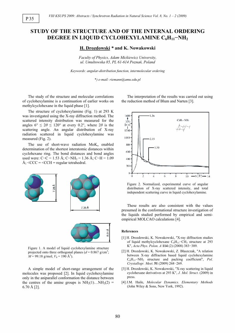
VIII KSUPS 2009: Abstracts / Synchrotron Radiation in Natural Science Vol. 8, No. 1 – 2 (2009)
80
STUDY OF THE STRUCTURE AND OF THE INTERNAL ORDERING DEGREE IN LIQUID CYCLOHEXYLAMINE C6H11−NH2
H. Drozdowski * and K. Nowakowski
Faculty of Physics, Adam Mickiewicz University, ul. Umultowska 85, PL 61-614 Poznań, Poland
Keywords: angular-distribution function, intermolecular ordering
*) e-mail: [email protected]
The study of the structure and molecular correlations of cyclohexylamine is a continuation of earlier works on methylcyclohexane in the liquid phase [1].
The structure of cyclohexylamine (Fig. 1) at 293 K was investigated using the X-ray diffraction method. The scattered intensity distribution was measured for the angles 6° ≤ 2θ ≤ 120° at every 0.2°, where 2θ is the scattering angle. An angular distribution of X-ray radiation scattered in liquid cyclohexylamine was measured (Fig. 2).
The use of short-wave radiation MoKα enabled determination of the shortest interatomic distances within cyclohexane ring. The bond distances and bond angles used were: C−C = 1.53 Å; C−NH2 = 1.36 Å; C−H = 1.09 Å; <CCC = <CCH = regular tetrahedral.
Figure 1. A model of liquid cyclohexylamine structure projected onto three orthogonal planes (d = 0.867 g/cm3; M = 99.18 g/mol; V0 = 190 Å3).
A simple model of short-range arrangement of the molecules was proposed [2]. In liquid cyclohexylamine only in the aniparallel conformation the distance between the centres of the amine groups is NH2(1)…NH2(2) = 6.70 Å [2].
The interpretation of the results was carried out using the reduction method of Blum and Narten [3].
Figure 2. Normalized, experimental curve of angular distribution of X-ray scattered intensity, and total independent scattering curve in liquid cyclohexylamine.
These results are also consistent with the values presumed in the conformational structure investigation of the liquids studied performed by empirical and semi-empirical MOLCAO calculations [4].
References
[1] H. Drozdowski, K. Nowakowski, "X-ray diffraction studies of liquid methylcyclohexane C6H11−CH3 structure at 293 K", Acta Phys. Polon. A 114 (2) (2008) 383−389.
[2] H. Drozdowski, K. Nowakowski, Z. Błaszczak, "A relation between X-ray diffraction based liquid cyclohexylamine C6H11−NH2 structure and packing coefficient", Pol. Crystallogr. Meet. 51 (2009) 268−269.
[3] H. Drozdowski, K. Nowakowski, "X-ray scattering in liquid cyclohexane derivatives at 293 K", J. Mol. Struct. (2009) in press.
[4] J.M. Haile, Molecular Dynamics. Elementary Methods (John Wiley & Sons, New York, 1992).
P 35
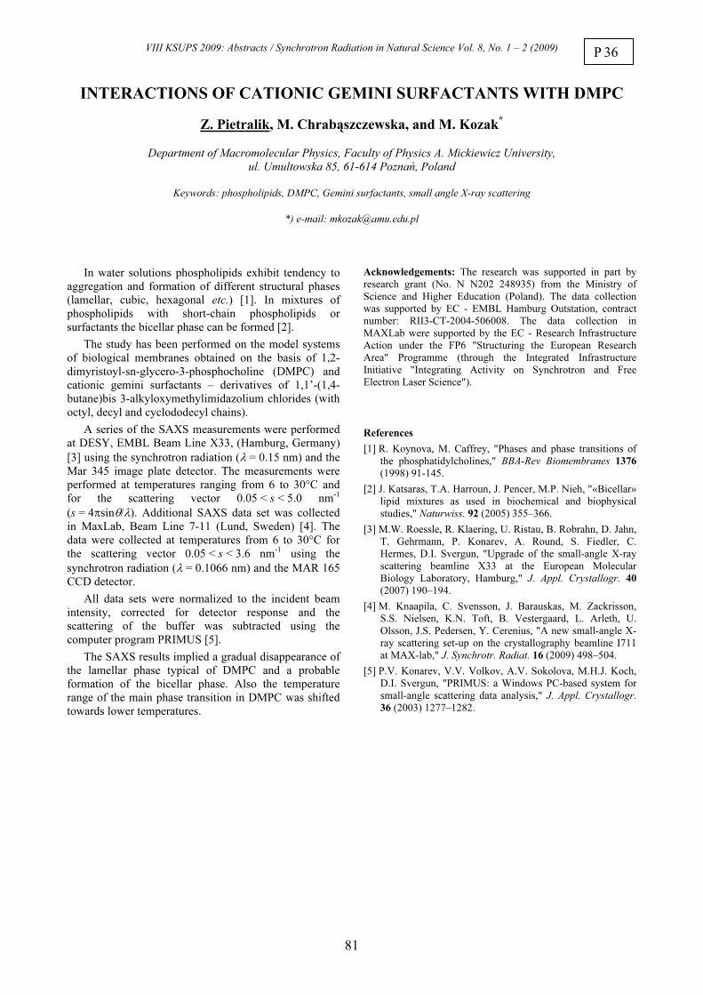
VIII KSUPS 2009: Abstracts / Synchrotron Radiation in Natural Science Vol. 8, No. 1 – 2 (2009)
81
INTERACTIONS OF CATIONIC GEMINI SURFACTANTS WITH DMPC
Z. Pietralik, M. Chrabąszczewska, and M. Kozak*
Department of Macromolecular Physics, Faculty of Physics A. Mickiewicz University,
ul. Umultowska 85, 61-614 Poznań, Poland
Keywords: phospholipids, DMPC, Gemini surfactants, small angle X-ray scattering
*) e-mail: [email protected]
In water solutions phospholipids exhibit tendency to
aggregation and formation of different structural phases
(lamellar, cubic, hexagonal etc.) [1]. In mixtures of
phospholipids with short-chain phospholipids or
surfactants the bicellar phase can be formed [2].
The study has been performed on the model systems
of biological membranes obtained on the basis of 1,2-
dimyristoyl-sn-glycero-3-phosphocholine (DMPC) and
cationic gemini surfactants – derivatives of 1,1’-(1,4-
butane)bis 3-alkyloxymethylimidazolium chlorides (with
octyl, decyl and cyclododecyl chains).
A series of the SAXS measurements were performed
at DESY, EMBL Beam Line X33, (Hamburg, Germany)
[3] using the synchrotron radiation (λ = 0.15 nm) and the
Mar 345 image plate detector. The measurements were
performed at temperatures ranging from 6 to 30°C and
for the scattering vector 0.05 < s < 5.0 nm-1
(s = 4πsinθ/λ). Additional SAXS data set was collected
in MaxLab, Beam Line 7-11 (Lund, Sweden) [4]. The
data were collected at temperatures from 6 to 30°C for
the scattering vector 0.05 < s < 3.6 nm-1 using the
synchrotron radiation (λ = 0.1066 nm) and the MAR 165
CCD detector.
All data sets were normalized to the incident beam
intensity, corrected for detector response and the
scattering of the buffer was subtracted using the
computer program PRIMUS [5].
The SAXS results implied a gradual disappearance of
the lamellar phase typical of DMPC and a probable
formation of the bicellar phase. Also the temperature
range of the main phase transition in DMPC was shifted
towards lower temperatures.
Acknowledgements: The research was supported in part by
research grant (No. N N202 248935) from the Ministry of
Science and Higher Education (Poland). The data collection
was supported by EC - EMBL Hamburg Outstation, contract
number: RII3-CT-2004-506008. The data collection in
MAXLab were supported by the EC - Research Infrastructure
Action under the FP6 "Structuring the European Research
Area" Programme (through the Integrated Infrastructure
Initiative "Integrating Activity on Synchrotron and Free
Electron Laser Science").
References
[1] R. Koynova, M. Caffrey, "Phases and phase transitions of
the phosphatidylcholines," BBA-Rev Biomembranes 1376
(1998) 91-145.
[2] J. Katsaras, T.A. Harroun, J. Pencer, M.P. Nieh, "«Bicellar»
lipid mixtures as used in biochemical and biophysical
studies," Naturwiss. 92 (2005) 355–366.
[3] M.W. Roessle, R. Klaering, U. Ristau, B. Robrahn, D. Jahn,
T. Gehrmann, P. Konarev, A. Round, S. Fiedler, C.
Hermes, D.I. Svergun, "Upgrade of the small-angle X-ray
scattering beamline X33 at the European Molecular
Biology Laboratory, Hamburg," J. Appl. Crystallogr. 40
(2007) 190–194.
[4] M. Knaapila, C. Svensson, J. Barauskas, M. Zackrisson,
S.S. Nielsen, K.N. Toft, B. Vestergaard, L. Arleth, U.
Olsson, J.S. Pedersen, Y. Cerenius, "A new small-angle X-
ray scattering set-up on the crystallography beamline I711
at MAX-lab," J. Synchrotr. Radiat. 16 (2009) 498–504.
[5] P.V. Konarev, V.V. Volkov, A.V. Sokolova, M.H.J. Koch,
D.I. Svergun, "PRIMUS: a Windows PC-based system for
small-angle scattering data analysis," J. Appl. Crystallogr.
36 (2003) 1277–1282.
P 36

VIII KSUPS 2009: Abstracts / Synchrotron Radiation in Natural Science Vol. 8, No. 1 – 2 (2009)
82
COMPOSITION AND STRUCTURE OF CZOCHRALSKI SILICON
IMPLANTED WITH H2
+ AND Mn
+ AND ANNEALED
UNDER ENHANCED HYDROSTATIC PRESSURE
M. Kulik 1, A.P. Kobzew
2, A. Misiuk
3, W. Wierzchowski
4, K. Wieteska
5,
J. Bak-Misiuk 6, A. Wnuk
3, and B. Surma
3
1 Institute of Physics, Maria Curie-Skłodowska University, Lublin, Pl. Marii Curie-Skłodowskiej 1, 20-031 Lublin, Poland
2 Joint Institute for Nuclear Research JINR, Joliot-Curie 6, 141980 Dubna, Moscow region, Russia 3 Institute of Electron Technology, Al. Lotników 46, 02-668 Warsaw, Poland
4 Institute of Electronic Materials Technology, 01-919 Warsaw, Poland 5 Institute of Atomic Energy, 05-400 Otwock-Świerk, Poland
6 Institute of Physics, PAS, Al. Lotników 32/46, 02-668 Warsaw, Poland
Keywords: Czochralski silicon, implantation, high pressure, diffraction
Depth distribution of implanted species and
microstructure of oxygen-containing Czochralski grown
silicon (Cz-Si) implanted with light (such as H+; Si:H is
important for so called smart cut processing [1]) or heavy
ions (such as Mn+; Si:Mn is considered as promising
material for spintronics [2]) are strongly influenced by
hydrostatic pressure (HP) applied during the post-
implantation treatment.
Composition and structure of Si:H (prepared by
implantation of Cz-Si with H2+; dose, D = 1.7×1017 cm-2,
energy, E = 50 keV, (projected range of H2+, Rp(H) = 275
nm) and of Si:Mn (implantation with Mn+; D = 1×10¹⁶
cm-2 , E = 160 keV, Rp(Mn) = 140 nm), processed at up
to 923 K under Ar pressure up to 1.2 GPa for up to 10 h,
were investigated by ERD, RBS, and photoluminescence
methods.
The defect structure of Si:Mn was also investigated
by synchrotron diffraction topography at HASYLAB
(Germany). High sensitivity to strain associated with
small inclusions and dislocation loops was provided by
monochromatic (l = 0.1115 nm) beam topography. High
resolution X-ray diffraction was also used.
As it follows from ERD measurements (Fig. 1), HP
applied during annealing of Si:H at 723--923 K affects
strongly the distribution of implanted hydrogen
preventing in part its out-diffusion.
Processing of Si:Mn under HP at up to 920 K for up
to 10 h did not produce resolved structure defects. On the
other hand, just such processing results in magnetic
ordering [3]. Synchrotron topography made it possible to
detect strains and large defects related to Si:Mn sample
bending and unhomogeneity.
References
1. A. Misiuk, A. Shalimov, B. Surma, J. Bak-Misiuk, A. Wnuk,
J. Alloys Comp. 401 (2005) 205.
2. A. Wolska, K. Lawniczak-Jablonska, M. Klepka, W.S.
Walczak, A. Misiuk, Phys. Rev. B 75 (2007) 113201.
3. W. Osinniy, A. Misiuk, M. Szot, K. Swiatek, J. Bak-Misiuk,
A. Barcz, W. Jung, Mater. Sci. - Poland 26 (2008) 751.
200 400 600
0
20
40
60
200 400 600 800
measured
Yie
ld [
cou
nts]
Channel number
Energy [keV]
H2
+
⇒ Si
tannealed
=650o
C, tannealed
=10 h
ERD
EHe
+=2297.00 keV
α = β = 75o
, θ = 30o
simulated
Figure 1. Typical spectrum of hydrogen measured by ERD methods.
P 37

VIII KSUPS 2009: Extended Abstracts / Synchrotron Radiation in Natural Science Vol. 8, No. 1 – 2 (2009)
83
HIGH-TEMPERATURE STUDIES OF Pb1-xCdxTe SOLID SOLUTION:
STRUCTURE STABILITY AND CdTe SOLUBILITY LIMIT
R. Minikayev 1
, E. Dynowska 1
, P. Dziawa 1
, E. Kamińska 2
,
A. Szczerbakow 1
, D. Trots 3, and W. Szuszkiewicz
1*
1 Institute of Physics, Polish Academy of Sciences, Al. Lotników 32/46, 02-668 Warsaw, Poland
2 Dept. of Mathematics and Natural Science, College of Science, Cardinal Stefan Wyszyński University,
ul. Dewajtis 5, 01-815 Warsaw, Poland 3 Institute for Materials Science, Darmstadt University of Technology,
Petersenstr. 23, D-64287 Darmstadt, Germany
Keywords: X-ray powder diffraction, lattice parameter, solubility limit, precipitate
*) e-mail: [email protected]
1. Introduction
The solid solution of lead telluride with cadmium telluride constitutes an attractive system for developing of the mid-IR optoelectronic devices based on quantum dots. The thermo-electric properties of Pb1-xCdxTe solution are also considered as a basis of other possible devices. These applications are powered by extremely low solubility of both materials [1] resulting from the difference in their crystal structure - rock-salt (RS) for PbTe and zinc-blende (ZB) for CdTe. It was a reason that only polycrystalline ternary Pb1-xCdxTe bulk samples obtained by Bridgman growth technique were so far available. Recently, the successful growth of Pb1-xCdxTe single crystals of 1 ccm volume with (100) natural crystal facets, and Cd content up to 11 at.% by self-selecting vapour transport method (SSVG) [2] has been reported [3]. In the latter paper the X-ray diffraction revealed the single-phase RS crystal structure of obtained samples and their relatively high crystal quality confirmed by FWHM of 004 X-ray rocking curve of about 100 arcsec. The decrease of the lattice parameter with increasing Cd content x had linear character with da/dx ≈ -0.43 Å for studied samples. The results of Hall effect and electrical conductivity measurements as well as the photoluminescence measurements were also obtained in the temperature range from 4.2 K to 300 K [3].
The goal of the present work was to study the structure properties of Pb1-xCdxTe solid solution at high temperatures (HT) and to get new information about the phase diagram corresponding to the system above mentioned.
2. Experimental details
In this work the analysis of selected structure properties of Pb1-xCdxTe (where x = 0; 0.013; 0.056; 0.096) were studied by X-ray diffraction measurements performed at temperatures ranging from 301 K to 1073 K. First, good quality single Pb1-xCdxTe crystals grown by SSVG method were powdered and analysed at room temperature (RT) using X’Pert Philips diffractometer and Cu Kα1 radiation. Later on, the HT measurements using a synchrotron radiation were carried out taking advantage of a powder diffractometer installed at the B2 beamline
at Hasylab/DESY. The instrumental parallel-beam set-up included a Ge(111) double monochromator, and a curved on-site readable imaging plate [4]. The samples were prepared as a mixture of powdered Pb1-xCdxTe crystals and fine diamond powder. For sample mounting a thin-wall quartz capillary was applied. During all measurements the capillary rotates inside a graphite hitter. The radiation wavelength, λ = 0.5276 Å, was calibrated in situ, using the diamond standard (advantages of such calibration method have been described in Ref. [5]). For the analysis of the diffraction patterns Rietveld method using the Fullprof.2k (v. 2.70) program was applied [6].
3. Results and discussion
The results of preliminary X-ray diffraction measurements performed at RT confirmed a single-phase (RS) character of all investigated Pb1-xCdxTe solid solutions. Figure 1 presents the composition dependence of the lattice parameter value determined in Ref. [3] (shown by the dashed line), values of the lattice parameters corresponding to the samples investigated in the present paper are marked by the open circles in this figure.
0.00 0.0 1 0.02 0.0 3 0 .04 0.0 5 0 .06 0.07 0 .08 0.09 0.10
6.420
6.425
6.430
6.435
6.440
6.445
6.450
6.455
6.460
a [Å
]
x
Figure 1. The initial lattice parameter value (determined
by X-ray diffraction) versus the chemical composition of
Pb1-xCdxTe solid solutions analysed in this paper. The
dashed line was taken from Ref. [3].
P 38

VIII KSUPS 2009: Extended Abstracts / Synchrotron Radiation in Natural Science Vol. 8, No. 1 – 2 (2009)
84
13.0 13.5 14 .0 14.5 15.0 15 .5 1 6.0 16.5
0
1
2
3
4
5
6
7D iam ond
111
Pb0, 94 4
Cd0 .05 6
T e
311 222
P b0,944
Cd0.0 56
Te
220
10 73 K
99 3 K
913 K
88 3 K
753 K
673 K
593 K
513 K
433 K
353 K
301 K
In
te
ns
ity
[a
.u.]
2Θ [o
]
Figure 2. The temperature-dependent peak shift for the sample containing
Pb0.944Cd0.056Te solid solution (the diffraction patterns at limited angular range
are shown).
Figure 2 shows a part of the temperature evolution of X-ray diffraction pattern taken with the use of synchrotron radiation for Pb0.944Cd0.056Te sample. As one can see, the angular shift of Bragg peaks corresponding to the solid solution under studies is slightly different below and above the temperature of about 650 K. The 111 reflection from diamond powder being the internal standard in the analyzed sample is also seen in this figure. The similar data were obtained for other investigated samples.
The example of the result of Rietveld refinement, performed for the diffraction pattern collected at T = 301 K is shown in Fig. 3. The high quality of the analysis taking into consideration the single phase character of Pb0.904Cd0.096Te solid solution and the diamond powder only excluded possible presence of other crystal phase in the investigated sample.
Figure 3. The Rietveld analysis of powder diffraction
pattern obtained for the sample containing Pb0.904Cd0.096Te
solid solution and the diamond powder. Points: the
experimental data taken with the use of synchrotron
radiation, solid line: theoretical curve. The first and the
second set of vertical bars correspond to Pb0.904Cd0.096Te
and diamond, respectively.
Due to the application of procedure above mentioned it was possible to demonstrate unexpected, non-monotonous temperature dependence of the lattice parameter value corresponding to every Pb1-xCdxTe sample with the initial x value different from zero. The comparison of dependences found for all measured samples is given in Fig. 4.
300 40 0 500 600 7 00 800 900 10 00 1100
6.42 0
6.43 5
6.45 0
6.46 5
6.48 0
6.49 5
6.51 0
6.52 5
6.54 0
6.55 5
6.57 0
a [Å
]
T [K]
Figure 4. The lattice parameter value versus temperature
for all Pb1-xCdxTe solid solutions analysed in this paper.
Full squares: x = 0; open squares: x = 0.013; circles: x =
0.056; triangles: x = 0.096.
The scenario of the temperature evolution of sample
structure, corresponding to Pb1-xCdxTe samples with x > 0 may be understood in the following manner. Due to a very rapid sample cooling from the growth temperature (being close to about 1100 K) to room temperature, applied in SSVG method [2, 3], a metastable solid solution was obtained. The exact chemical composition of this solution, determined prior to the accompagned by the HT studies with the use of synchrotron radiation, was far from that corresponding to the solubility limit. Thus, the ‘initial’ sample composition reflected the HT,‘frozen’ equilibrium state of the solid solution. A partial decomposition of the sample was clearly observed as the

VIII KSUPS 2009: Extended Abstracts / Synchrotron Radiation in Natural Science Vol. 8, No. 1 – 2 (2009)
85
result of increasing sample temperature from about 500 K to 650 K. This effect was indicated by the increase of the lattice parameter significantly higher than the linear one expected on the basis of our data determined for pure PbTe (see Fig. 4). It means that some part of Cd present at the beginning in Pb1-xCdxTe solid solution is missing at higher temperatures. The same time possible creation of the second crystal phase (like, e.g., Cd, Te, or ZB CdTe) was not observed. Due to the lack of new crystal phase at this temperature range one may suppose a creation of an amorphous CdTe precipitates or clusters in the sample. The minimal chemical composition of every solid solution, observed in the present studies, was close to x = 0.01 and corresponded to the temperature of about 650 K. It should be stressed that this composition value does not depend on the ‘initial’ sample composition, as it was demonstrated in Fig. 4. This finding may be interpreted as the real CdTe solubility limit in PbTe for the temperature indicated above. Further increase of temperature resulted in a partial dissolution of CdTe in Pb1-xCdxTe and finally at some, high temperature the final solid solution composition was about the same as that at the beginning of measurements. One may suppose that at this last temperature the second phase (not visible in the diffraction patterns) disappears and the solid solution under investigation starts to be once more one-phase and uniform material. The only exception was the sample initially determined as Pb0.904Cd0.096Te solid solution. After the measurements performed at high temperatures and cooling down this sample back to RT the ZB CdTe precipitates were observed and the chemical composition of the final solid solution was estimated as equal to x ≈ 0.08.
The scenario described above is not new. The possible creation of temperature activated precipitates in systems composed of two substances characterized by a broad miscibility gap has been reported and discussed in the literature for a few systems composed of selected II-VI and IV-VI semiconducting compounds exhibiting ZB (or wurtzite) structure and RS structure, respectively [7-10]. The new results presented in this paper completed published previously phase diagram for PbTe-CdTe system [8, 11] limited in the past to temperatures above 870 K and solid solution compositions exceeding the value x = 0.05.
4. Conclusions
Due to the access to bulk Pb1-xCdxTe solid solution it was possible to contribute to the phase diagram of this system for x < 0.1 and T < 1100 K. In particular, new
information concerning the CdTe solubility limit in PbTe was obtained. Such findings may have important influence on the optimization of material devoted to possible future applications.
Acknowledgements: The research leading to these results has
received funding from the European Community's Seventh
Framework Programme (FP7/2007-2013) under grant
agreement n° 226716. Partial financial support of RM, ED, and
WSz by the Ministry of Sciences and Higher Education
(Poland) through grant DESY/68/2007 is also acknowledged.
References
[1] T. Schwarzl, E. Kaufmann, G. Springholz, K. Koike, T.
Hotei, M. Yano, W. Heiss, "Temperature-dependent
midinfrared photoluminescence of epitaxial PbTe/CdTe
quantum dots and calculation of the corresponding
transition energy", Phys. Rev. B 78 (2008) 165320.
[2] A. Szczerbakow, K. Durose, "Self-selecting vapour growth
of bulk crystals – principles and applicability ", Prog.
Cryst. Growth Charact. Mater. 51 (2005) 81.
[3] M. Szot, A. Szczerbakow, K. Dybko, L. Kowalczyk, E.
Smajek, M. Bukała, M. Galicka, P. Sankowski, R. Buczko,
P. Kacman, V. Domukhovski, E. Łusakowska, P. Dziawa,
A. Mycielski, T. Story, "Experimental and theoretical
analysis of PbTe-CdTe solid solution grown by physical
vapour transport method", Acta Phys. Pol. A (in press).
[4] M. Knapp, C. Baehtz, H. Ehrenberg, H. Fuess, "The
synchrotron powder diffractometer at beamline B2 at
HASYLAB/DESY: status and capabilities", J. Synchr.
Radiation 11 (2004) 328.
[5] W. Paszkowicz, M. Knapp, C. Bähtz, R. Minikayev, P.
Piszora, J.Z. Jiang, R. Bacewicz, "Synchrotron X-ray
wavelength calibration using a diamond internal standard:
application to low-temperature thermal-expansion studies ",
J. Alloys Compds 382 (2004) 107.
[6] J. Rodriguez-Carvajal, "Line Broadening analysis using
FullProf*: determination of microstructural properties",
Newslett. IUCr Commission Powd. Diffr. 26 (2001) 12.
[7] V. Leute, N.J. Haarmann, H.M. Schmidtke, "Solid state
reactions in the quasiternary system (Cd, Pb)(S, Te)", Z.
Phys. Chem. 190 (1995) 253.
[8] V. Leute, R. Schmidt, "The quasiternary system
(CdkPb1-k)(SlTe1-l)", Z. Phys. Chem. 172 (1991) 81.
[9] V. Leute, A. Jamour, "Double conversions between PbS-
single crystals and polycrystalline CdTe in solid state", J.
Phys. Chem. Solids 32 (1971) 1435.
[10] H.M. Schmidtke, V. Leute, "Investigation of the reaction
between a CdSe-crystal and a Pb and S containing reactive
gas phase", J. Phys. Chem. Solids 45 (1984) 547.
[11] N.Kh. Abrikosov, Semiconducting II-VI, IV-VI, and V-VI
Compounds (Plenum Press, New York, 1969).

VIII KSUPS 2009: Abstracts / Synchrotron Radiation in Natural Science Vol. 8, No. 1 – 2 (2009)
XRD STUDIES OF NB/SAPPHIRE(001) THIN FILMS DEPOSITED
WITH THE ULTRA-HIGH-VACUUM CATHODIC ARC TECHNIQUE
R. Nietubyć 1*, W. Caliebe 2, E. Dynowska 3, K. Nowakowska-Langier 1,
J. Pełka 3, and P. Romanowski 3
1 The Andrzej Soltan Institute for Nuclear Studies, Świerk, Poland2 Hasylab at DESY, Notkestr. 85, D-22603 Hamburg, Germany
3 Institute of Physics PAS, Warsaw, Poland
Keywords: thin metallic films, x-ray diffraction
*) e-mail: [email protected]
Niobium films on the single crystal substrate have
been studied. The films of thicknesses less than 5 nm,
5 nm, 15 nm and 400 nm were deposited onto sapphire
(001) surface by mean of the cathodic arc in UHV
conditions [1-3]. Energy of incoming Nb3+ions in the
range of tens electronovolts and substrate temperature
about 200°C are distinctive characteristics of that
deposition method. The aim of performed XRD studies
was to recognize the structural forms of Nb film formed
in the early stages of growth. The measurements were
preformed at the wiggler beamline W1 using the photon
energy 8048 eV corresponding to the wavelength
λ = 0.15406 nm (Cu Kα1 characteristic line).
According to our studies, the growth of Nb layer is
realized in three stages: the first one is the growth of very
thin and preferably (110)-oriented layer. In the next
stage an increasing of the layer thickness lead to the
almost single crystal layer with (110) lattice planes
parallel to the substrate surface. In the last stage,
observed for the thickest layer, the appearance of thin
polycrystalline Nb layer, probably on the surface, have
been observed.
References
[1] R. Nietubyc, J. Pelka, M.J. Sadowski, P. Strzyżewski, AIP
Conf. Proc. 993 (2008) 415.
[2] P. Strzyzewski, M.J. Sadowski, R. Nietubyc, K. Rogacki,W.
Paszkowski, T. Paryjczak, J. Rogowski, Mater. Sci.–
Poland 26 (2008) 213.
[3] J. Langner, R. Mirowski, M.J. Sadowski, P. Strzyżewski, J.
Witkowski, S.Tazzari, L. Catani, A. Cianchi, J. Lorkiewicz,
R. Russo, Vacuum 80 (2006) 1288.
Figure 1. The growth of Nb film as seen with the x-ray eye.
86
P 39

VIII KSUPS 2009: Abstracts / Synchrotron Radiation in Natural Science Vol. 8, No. 1 – 2 (2009)
87
COLLOIDAL ZnO AND ZnO/MgO CORE/SHELL NANOCRYSTALS - SYNTHESIS AND PROPERTIES
B. Sikora, A. Baranowska-Korczyc, W. Zaleszczyk, A. Nowicka, K. Fronc, W. Knoff, K. Gas, W. Paszkowicz, W. Szuszkiewicz, K. Świątek, Ł. Kłopotowski, K. Sobczak,
P. Dłużewski, G. Karczewski, T. Wojtowicz, I. Fijałkowska, and D. Elbaum
Institute of Physics, Polish Academy of Sciences, Al. Lotników 32/46 02-668 Warsaw, Poland
Keywords: zinc oxide, , nanoparticles, nanocrystals, quantum dots
*) e-mail: [email protected]
ZnO nanocrystals nad ZnO/MgO core/shell nanocrystals have interesting biological properties (antibacterial, antifungal). ZnO nanocrystals have recently attracted a lot of attention as promising candidates for novel devices, due to a possibility of continuous tuning of optical and electronic properties by varying the particle sizes. They are also of interest for pharmaceutical industry, medicine and/or biology. Obtained nanocrystals were characterized structurally by Atomic Force Microscopy (AFM), Transmission Electron Microscopy (TEM) (Fig 1), X-ray diffraction (Fig. 2) and optically by absorption and emission.
Figure 1. Transmission Electron Microscopy of the ZnO nanocrystals proved a wurtzite crystalline structure. We prepared ZnO nanocrystals in colloidal
suspensions using a sol–gel method. The growth was carried out in various solvents, different incubation times, and temperatures. By measuring the absorbance, and emission of the nanocrystals solution, we monitored the growth. We observed a decrease of the reaction activation energy with an increase in the polarity of the applied solvent. Therefore, the growth rate was higher in a solvent with greater dielectric constant. With increasing nanocrystal sizes the absorption onset was red-shifted. An effective mass approximation model [1] was used to determine the nanocrystal radii. The results were compared with sizes obtained from AFM analysis and a good correlation was found. Depending on conditions and reaction time, we obtained nanocrystals with radii ranging from 2 to 5 nm. Photoluminescence spectra
revealed two emission bands. One (narrow 10 nm line width), observed around 375 nm, due to a band-to-band recombination. This PL line behaved analogously to the absorption onset, red-shifted with increasing nanocrystal size. The other emission band was a broad (100 nm line width), centered around 530 nm, probably related to oxygen vacancies.
Addition of MgO shell resulting in a more intense and stable visible emission that is characteristic of nanocrystalline ZnO. MgO prevents aggregation of ZnO nanoparticles.
XRD patterns of powdered ZnO/MgO nanocrystals and TEM data proved wurtzite crystalline structure.
0 20 40 60 80 100 120
0
2000
4000
6000
8000
10000
12000
14000
16000
18000
Inte
nsity
(arb
. uni
ts)
2θ (o)
Mg/Zn = 18% Mg/Zn = 56 % Mg/Zn = 37%
100
002 101
102110
103200
Figure 2. X-ray diffraction pattern (wavelength 1.54060 Å) for ZnO/MgO core/shell powder as a function of thickness shell. The Zn:Mg ratio was: 18%, 37% and 56%. The results proved the wurtzite crystalline structure.
Acknowledgements: The research was partially supported by the European Union within European Regional Development Fund, through grant Innovative Economy (POIG.01.01.02-00-008/08) and was partially supported by the Ministry of Science and Higher Education (Poland) through Grant No. N515 015 32/0997 and No. N N518 424036.
References
[1] S. Monticone, R. Tufeu, A.V. Kanaev, "Complex nature of the UV and visible fluorescence of colloidal ZnO Nanoparticles", J. Phys. Chem. B. 102 (1998), 2854–2862.
P 40

VIII KSUPS 2009: Extended Abstracts / Synchrotron Radiation in Natural Science Vol. 8, No. 1 – 2 (2009)
ZnO NANOFIBERS PREPARED BY ELECTROSPINNING— CHARACTERIZATION AND DOPING
A. Baranowska-Korczyc*, B. Sikora, W. Zaleszczyk, A. Nowicka, K. Fronc, W. Knoff, P. Dziawa, K. Gas, W. Paszkowicz, R. Minikayev, W. Szuszkiewicz, K. Świątek,
T. Wojciechowski, A. Reszka, Ł. Kłopotowski, K. Sobczak, P. Dłużewski, G. Karczewski, T. Wojtowicz, J. Bujak, and D. Elbaum
Institute of Physics, Polish Academy of Sciences, Al. Lotników 32/46, 02-668 Warsaw, Poland
Keywords: zinc oxide, nanowire
*) e-mail: [email protected]
Figure 1. XRD result of ZnO nanofibers (calcinationtemperature: 500ºC).
Electrospinning is a method capable to produce fiberswith diameters ranging from tens of nanometer tomicrons. Electrospun nanofibrous scaffolds have greatpotential in several biomedical applications, such aswound dressing, enzyme immobilization, drug delivery,tissue engineering, and they can serve as materials forbiosensors. Semiconductor nanofibers are also candidatesfor applications in electronics and optoelectronics.
We synthesized zinc oxide (ZnO) nanofibers by sol-gel processing. The first step was to form the nanofibresby electrospinning technique using a suspension of zincacetate in poly(vinyl alcohol) (PVA) or poly(ethyleneoxide) (PEO) as precursors. Then, the nanofibres werecalcined in air at 500º, 600º, 700ºC [1] for 4 h to obtainZnO nanofibers [2, 3]. By adding acetates of othermetals, we obtained nanofibers doped with Co, Fe, Al,Mn, Mg.
Structural characterization was performed by AtomicForce Microscopy (AFM), Scanning ElectronMicroscopy (SEM), and X-ray diffraction (XRD).Additionally, optical characterization was done bycathodoluminescence (CL) and photoluminescence (PL)measurements at room temperature.
XRD investigations proved that the nanofibermaterial is a wurtzite ZnO (Fig. 1, Fig. 2). AFM and
Figure 2. XRD result of Co, Mn, Mg and Fe doped ZnOnanofibers (calcination temperature: 500ºC).
SEM studies both revealed nanofiber diameters rangingfrom 100 to 300 nm. Moreover, SEM images of undopedZnO show that the nanofibers consist of nanocrystalliteswhich diameters from 10 to 50 nm as jointly determinedby XRD and SEM (Fig. 3). However, metal-dopednanofibers contain significantly smaller nanocrystallites.
Figure 3. SEM image of ZnO nanofibers (calcinationtemperature: 500ºC).
88
P 41

VIII KSUPS 2009: Extended Abstracts / Synchrotron Radiation in Natural Science Vol. 8, No. 1 – 2 (2009)
89
Figure 4. SEM image of ZnO nanofibers (calcination
temperature: 700ºC).
PL spectra of undoped nanofibers consist of two
emission bands. One, centered around 390 nm, is due to
ZnO band-to-band recombination. The other one, a
defect band 200 nm wide centered around 550 nm most
probably originates from oxygen vacancies. These
emission lines are absent in PL spectra of Co-doped
nanofibers. In this case, the emission is dominated by an
intra-Co transition at 689 nm, proving that Co ions are
incorporated into ZnO lattice. Moreover, preliminary PL
studies of single nanofibers were performed.
The effect of ZnO nanofibers calcination temperature
was investigated by SEM. We observed increased crystal
size (cf. Fig. 4) and investigated the evolution of CL
spectra with growing calcination temperatures.
Acknowledgements: The research was partially supported by
the European Union within European Regional Development
Fund, through grant Innovative Economy (POIG.01.01.02-00-
008/08) and was partially supported by the Ministry of Science
and Higher Education (Poland) through Grant No. N515 015
32/0997.
References
[1] J.Y. Park, S.S. Kim, "Growth of nanograins in electrospun
ZnO nanofibers," J. Am. Ceram. Soc. 92 (2009) 1691–1694.
[2] H. Wu, D. Lin, R. Zhang, W. Pan, "ZnO nanofiber field-
effect transistor assembled by electrospinning," J. Am.
Ceram. Soc. 2 (2008) 656–659.
[3] H.R. Siddheswaran, R. Sankar, M. Ramesh Babu, M.
Rathnakumari, R. Jayavel, P. Murugakoothan, P.
Sureshkumar, "Preparation and characterization of ZnO
nanofibers by electrospinning," Cryst. Res. Technol. 41
(2006) 446–449.

VIII KSUPS 2009: Abstracts / Synchrotron Radiation in Natural Science Vol. 8, No. 1 – 2 (2009)
90
SOLUTION STRUCTURE OF RAR1-GST-TAG FUSION PROTEIN
M. Kozak 1*, M. Taube 1, E. Banachowicz 2, and A. Jarmołowski 3
1 Department of Macromolecular Physics, Faculty of Physics, A. Mickiewicz University,
ul. Umultowska 85, 61-614 Poznań, Poland 3 Department of Gene Expression, Institute of Molecular Biology and Biotechnology, Faculty of Biology,
A.Mickiewicz University, Umultowska 89, 61-614 Poznań, Poland 2 Molecular Biophysics Division, Faculty of Physics, A.Mickiewicz University,
ul. Umultowska 85, 61-614 Poznań, Poland
Keywords: small angle X-ray scattering, solution structure, Rar1
*) e-mail: [email protected]
Plants are able to recognize pathogen attack and respond to them by R gene triggered resistance and cell death [1, 2]. Rar1 protein is a common element of signaling pathways in those processes.
Rar1 is a small, monomeric protein (for example Rar1 from Hordeum vulgare is characterized by molecular mass of 25.5 kDa and polypeptide chain is build of 232 amino acid residues). Sequence consist of two 60-amino acid zinc binding domains (CHORDs), located on the C- and N-terminus of the protein [1]. In plants a highly conserved motif between those two regions can be found. It is also a zinc binding motif, containing three invariant cysteine and a histidine residues.
At molecular level Rar1 interacts with two important proteins - suppressor of the G2 allele of Skp1 (SGT1) and heat-shock protein 90 (HSP90) via respectively CHORDI and CHORDII domains [2].
The low-resolution structure and conformation of Rar1-Glutathione S-transferase-tag fusion protein from barley in solution has been studied by small angle scattering of synchrotron radiation (SAXS).
SAXS measurements were preformed on the X-33 EMBL beamline at DESY, Hamburg (Germany) using the Pilatus photon counting detector. Protein samples (4.7, 7.5, 15.3 mg/ml) were measured in 50 mM Tris/HCl pH 7.6 using synchrotron radiation (wavelength λ=0.15 nm) at temperature 283 K. The sample-to-detector distance was 1.7 m, corresponding to the scattering vector range form 0.057 to 5.178 nm-1 (s = 4πsinθ/λ where 2θ is the scattering angle).
The overall structural parameters characterizing molecule, such as maximum diameter Dmax and radius of gyration were computed using GNOM. The Rar-1-GST fusion protein forms in solution dimers characterized by RG= 6.19 nm and Dmax = 23 nm.
Using experimental SAXS curve also the 3D model has been reconstructed using ab initio methods and program DAMMIN [3]. The exemplary low resolution model in solution is presented in Fig. 1.
We also compared the low resolution model of particle with structure predicted by homology-modelling using SWISS-MODEL (www.expasy.ch).
Figure 1. Low-resolution model of Rar1-Glutathione S-transferase-tag fusion protein in solution reproduced by DAMMIN.
Acknowledgements: The data collection was supported by European Community - EMBL Hamburg Outstation, contract number: RII3-CT-2004-506008.
References
[1] K. Shirasu, T. Lahaye, M.W. Tan, F. Zhou, C. Azevedo, "A novel class of eukaryotic zinc-binding proteins is required for disease resistance signaling in barley and development in C. elegans," Cell 99 (1999) 355−366.
[2] C.T. Heise, C.S. Le Duff, M. Boter, C. Casais, J.E. Airey, A.P. Leech, B. Amigues, R. Guerois, G.R. Moore, K. Shirasu, C. Kleanthous, "Biochemical characterization of Rar1 cysteine- and histidine-rich domains (CHORDs): A novel class of zinc-dependent protein−protein interaction modules," Biochem. 46 (2007) 1612−1623.
[3] D.I. Svergun, "Restoring low resolution structure of biological macromolecules from solution scattering using simulated annealing," Biophys. J. 76 (1999) 2879−2886.
P 42

K. Jablonska / Synchrotron Radiation in Natural Science Vol. 8, No. 1– 2 (2009)
91
Membership of Poland in ESRF
Starting from year 2004, Poland is an Associated Member of the European Synchrotron Radiation Facility (ESRF) in Grenoble, France. Nevertheless, one should remember that this is not given us for ever. In July 2006, a three-years project for financing the participation of Poland at the level of 1% of ESRF budget was approved by Ministry of Science and Poland joined 25 European countries (including Israel) belonging to ESRF. Since that date, for the scientists from Polish academic and scientific institutions applications for beamtime at the ESRF experimental stations became possible. Prof. K. Jablonska was the leader of the project which was allocated at the Institute of Physics Polish Academy of Science in Warsaw. This project ended in June 2009. The web page of the Polish membership in ESRF can be found at http://info.ifpan.edu.pl/esrf/Local_Publish/, where all useful information about the project are collected.
In order to get financing of Polish contribution to ESRF for next two years, it was necessary to apply for funds to Ministry of Science and High Education in the beginning of 2009. In the application, a report from the project presenting the scientific output from the experiments performed at ESRF had to be prepared. In the Table 1 and histogram (see Fig. 1) the readers can find information about the interest of Polish scientists to the use of ERSF in number of shifts applied from all countries and from Poland and number of shifts available at ESRF and allocated for Polish scientists. As one can see, there is an interest in Polish scientific community in use of this source of radiation and we are quite successful in getting access to ESRF.
Table 1. Shifts allocated for Poland.
Year All applications
Applications from Poland
Available in ESRF
Allocated for Poland
shifts shifts percent shifts shifts percent2006/II 15 570 364 2.3% 6 852 180 2.6 %2007 29 959 598 2.0% 13 681 240 1.75%2008 31 105 661 2.1% 13 836 204 1.5 %
Shifts
192
99117
73
99
186
90
159
90 93
0
50
100
150
200
250
2006 / II 2007 / I 2007 / II 2008 / I 2008 II
Num
ber
Requested Allocated
Figure 1. Time evolution of shifts requested (left) and allocated (right) for Poland.
Moreover, the Ministry has asked for various details concerning the use of ESRF; we provided them with the list of institutions contributing in the projects and the corresponding numbers of used shifts. 40 institutions participated in the applications but the final number of beneficent was lower as not all projects have been accepted. In many cases in one project several institutions participated.
We have been asked also to present a list of publications resulting from performed experiments together with the corresponding journal impact factors as well as a list of conference presentations, doctoral theses etc. Unfortunately, the lack of answers from project participants (despite several reminders sent by e-mail) led to a risk of failure of the continuation of financing. I would like to thank Wojciech Paszkowicz for his extensive searching of internet and databases and collecting information about 84 papers published from experiments performed at ESRF. Only due to reporting of so successful output from the ESRF project the approval was received and we are happy to inform that the Ministry has decided to extend the project for next two years. In 2011 it will be necessary to apply again and to again prove that the funds spent for Polish contribution give reasonable scientific profit. Therefore, I would to ask all of ESRF users to remember about regular visiting the web page of the project and to systematically inform us about all papers, doctoral theses and conference presentations with contribution of data collected at ESRF. In all published information the grant ESRF/73/2006 must be explicitly acknowledged. Following this way and providing the data on publications is crucial for the further access to ESRF. The access to ESRF, although limited and concerning a light source of specific characteristics, is even more important considering fact that policy of the European Union is directed towards strong limitation of the open access to large facilities. So both, the national light sources and the experimentalists using them are expected to loose the financing which helped them in the first decade of 21st century. Moreover, one of machines, DORIS III synchrotron in Hamburg, will be closed in 2012. Unfortunately, the number of beamlines at the replacing Petra ring will be much smaller.
It is a pleasure for me to inform you that Poland being the associated member, for the first time has a representation in the Scientific and Advisory Committee of ESRF. For the three years turn Prof. Mariusz Jaskólski (Poznań) was elected in May 2009 as a representative of all associated members. Moreover, at the 51th ESRF Council meeting in June 2009, it was approved that an associated country can be owner of a national beamlines at ESRF (so called CRG stations). Therefore, new possibilities are in front of us. All is in our hands!!!
K. Jablonska

Synchrotron Radiation in Natural Science Vol. 8, No. 1– 2 (2009)
10th International School and Symposium on Synchrotron Radiation in Natural Sciences
ISSRNS 2010
Szklarska Por�ba 2010
Conference site: Hotel LAS fot. Hotel „LAS”
The 10th jubilee International School and Symposium on Synchrotron Radiation in Natural Science (ISSRNS’2008) will be organized by Polish Synchrotron Radiation Society (PTPS) (www.synchrotron.org.pl) in cooperation with Adam Mickiewicz University (Poznan, Poland) (www.amu.edu.pl) in hotel “LAS” in Szklarska Poreba (Poland) on 6-12 June 2010.
ISSRNS is a traditional forum for discussing fundamental issues of application of the synchrotron radiation and related methods in natural sciences. The aim of this interdisciplinary meeting is to bring together scientists working with synchrotron radiation. The Symposium will focus on novel applications of synchrotron radiation in physics, chemistry, material and live sciences.
The meeting will be held in the comfortable hotel “LAS” (www.hotel-las.pl) located in Szklarska Poreba (the town near Jelenia Gora, Lower Silesian Voivodeship). Szklarska Por�ba is situated in the south-western part of Poland in Karkonosze and Izery mountain range, in the vicinity of large central European cities with international airports (Prague 139 km, Wroc�aw 140 km away, Dresden 180 km).
Szklarska Por�ba region is place know of occurrence of precious ores. There have been classified over 50 minerals, which commonly occur in Karkonosze and Izery mountains. Many of them present properties of such gemstone as: amethyst,
aventurine, topaz, olivine, tourmaline, aquamarine, hyacinth, beryl, moonstone, agate, mountain crystal and smoky quartz. Therefore this beautiful town is known as the Mineralogical Capital of Poland.
Szklarska Por�eba is also an important regional and national centre for mountain hiking, cycling and skiing.
The topics of the meeting will cover main areas of applications of synchrotron radiation:
- macromolecular crystallography, - scattering techniques in structural analysis of
condensed matter, - x-ray absorption, fluorescence and photoelectron
spectroscopies, - x-ray magnetic dichroism, - x-ray diffraction - applications of synchrotron radiation in soft
matter physics, - synchrotron radiation in nanosciences, - synchrotrons, free electron lasers and alternative
radiation sources - design and development. The programme of the Symposium will
comprise invited lectures, oral communications (20 minutes) and poster presentations. The abstracts of all presentations presented on ISSRNS will be published in a volume of Synchrotron Radiation in Natural Science, and the proceedings in a reputable international journal. The official language of the meeting is English.
92

Synchrotron Radiation in Natural Science Vol. 8, No. 1– 2 (2009)
International Advisory Board
Francesco d'Acapito - European Synchrotron Radiation Facility, Grenoble, France
Edward Goerlich - Jagellonian University, Kraków, Poland
Jürgen Härtwig - European Synchrotron Radiation Facility, Grenoble, France
Mariusz Jaskólski - Center for Biocrystallographic Research, Polish Academy of Sciences, Poznan, Poland
Andrzej Kisiel - Jagellonian University, Kraków, Poland
Peter Laggner - Institute of Biophysics and Nanosystems Research, Graz, Austria
Andrea Lausi - Sincrotrone Trieste, Trieste, Italy
Jarosław Majewski - Los Alamos National Laboratory, USA
Giorgio Margaritondo - Ecole Polytechnique Federale de Lausanne, Switzerland
Gerhard Materlik - Diamond Light Source, Didcot, United Kingdom
Bronisław Orłowski - Institute of Physics, Polish Academy of Sciences Warszawa; Polish Synchrotron Radiation
Society, Poland
Adam Patkowski - A. Mickiewicz University, Poznań, Poland
Christian Riekel - European Synchrotron Radiation Facility, Grenoble, France
Leonid Rivkin - LPAP Swiss Federal Institute of Technology Lausanne, Paul Scherrer Institute Villigen, Switzerland
Masaki Taniguchi - Hiroshima Synchrotron Radiation Center, Hiroshima University, Japan
Ernst Weihreter - Helmholtz-Zentrum Berlin, Elektronenspeicherring BESSY II, Germany
Alexander Wlodawer - Macromolecular Crystallography Laboratory NCI-Frederick, Frederick, USA
Organizing Committee
Maciej Kozak (Chairman) - A. Mickiewicz University, Poznań, Poland
Wojciech Kwiatek -Institute of Nuclear Physics, Polish Academy of Sciences, Kraków, Poland
Wojciech Paszkowicz - Institute of Physics, Polish Academy of Sciences, Warsaw, Poland
Paweł Piszora - A. Mickiewicz University, Poznań, Poland
Krystyna Jablonska - Institute of Physics,Polish Academy of Sciences, Warsaw, Poland
Kamil Szpotkowski - A. Mickiewicz University, Poznań, Poland
Michał Taube - A. Mickiewicz University, Poznań, Poland
Zuzanna Pietralik - A. Mickiewicz University, Poznań, Poland
For further information, post or e-mail to:
Maciej Kozak
ISSRNS 2010
Department of Macromolecular Physics
Faculty of Physics
A. Mickiewicz University
Umultowska 85
61-614 Poznań
Poland
Phone. 0048-61-8295266
Fax: 0048-61-8295245
e-mail : [email protected]
website: www.10issrns.amu.edu.pl
93

Synchrotron Radiation in Natural Science Vol. 8, No. 1– 2 (2009)
94
Wspomnienie
Prof. nzw. U.W. dr hab. Jerzy Gronkowski (1949 – 2009)
Z wielkim bólem i żalem żegnamy Jerzego Gronkowskiego, zmarłego 6 lutego 2009 r., po przegranej walce z bardzo ciężką chorobą. Był naszym serdecznym, bardzo życzliwym kolegą, a od 1997 r. – naszym przełożonym.
Prof. Jerzy Gronkowski, wychowanek VI Liceum im. Jana Kochanowskiego w Radomiu, podjął po maturze studia na Wydziale Fizyki Uniwersytetu Warszawskiego, które ukończył w roku 1971. Pracę magisterską wykonywał w Pracowni Rentgenowskiej Zakładu Ciała Stałego Instytutu Fizyki Doświadczalnej, kierowanego przez prof. Leonarda Sosnowskiego. W październiku 1971 r. został zatrudniony w Instytucie Fizyki Doświadczalnej Wydziału Fizyki U.W. na stanowisku asystenta.
Całe swoje życie naukowe związał z naszym Zakładem Badań Strukturalnych, który w 1974 r. został utworzony z Pracowni Rentgenowskiej Zakładu Fizyki Ciała Stałego. Poświęcił się tematyce dyfrakcji promieni X w monokryształach i badaniom defektów sieci krystalicznej. Stopień doktora uzyskał w 1979 r. na Wydziale Fizyki Uniwersytetu Warszawskiego. Tematyką jego pracy doktorskiej, wykonywanej pod kierunkiem prof. Juliana Auleytnera, było badanie kontrastu dyfrakcyjnego dyslokacji w monokrysztale Si w przypadku Bragga dla fali padającej płaskiej. Struktura subtelna kontrastu dyfrakcyjnego dyslokacji w monokryształach Si była przedmiotem kolejnych jego prac.
W roku akademickim 1981/1982 odbył staż naukowy w Laboratorium Mineralogii Krystalografii Uniwersytetu im. Marii i Piotra Curie, Paris VI, kierowanym przez prof. A. Authiera. Współpracował wtedy z prof. Cecile
Malgrange, rozwijając teorię dyfrakcji promieni X w kryształach zdeformowanych, dla przypadku Bragga. Przebywał potem na kilkumiesięcznych stażach w tym samym Laboratorium w latach 1989 – 1999.
Na podstawie uzyskanych wyników, dotyczących rozwijanej w ramach tej współpracy tematyki, otrzymał stopień doktora habilitowanego na Wydziale Fizyki Uniwersytetu Warszawskiego w roku 1992.
Po uzyskaniu stopnia doktora habilitowanego prowadził badania mikrodefektów rozłożonych statystycznie w monokryształach oraz w układach wielowarstwowych, stosując metody wysokorozdzielczej dyfraktometrii rentgenowskiej oraz topografii rentgenowskiej. Rozwijał aparat teoretyczny i numeryczny niezbędny do ścisłego opisu tych zjawisk i stosowanych metod pomiarowych. W toku tych prac rozpoczął badania wpływu stopnia spójności wiązki padającej na obserwowane wyniki (np. na obraz otrzymywany w topografii przekrojowej) i rozważał zmiany tego stopnia wywołane przez mikrodefekty rozłożone statystycznie w kryształach.
Jego działalność naukowa zaowocowała publikacją około 80-ciu prac. Dla celów dydaktyczno-popularyzatorskich opublikował artykuł w Postępach Fizyki w 1986 r. „Promieniowanie Synchrotronowe – nowe perspektywy rozwoju metod rentgenowskich”, który stał się bardzo przydatny dla studentów, dając podstawy wiedzy o tym cennym narzędziu badawczym.
Prof. Jerzy Gronkowski był bardzo dobrym dydaktykiem. Prowadził zajęcia na Pracowni Fizycznej I, gdzie przejawiał dużo inwencji, ustawiając nowe ćwiczenia.

Synchrotron Radiation in Natural Science Vol. 8, No. 1– 2 (2009)
95
Za Jego duży wkład w rozwój Pracowni Fizycznej I otrzymał w r.1981 nagrodę dydaktyczną wraz z M. Bardadin-Otwinowską. K. Pniewską i M. Iżyckim.
Przez wiele lat prowadził ćwiczenia z dyfrakcji promieni X na Pracowni Fizycznej dla Zaawansowanych (tzw. Pracowni II). Kształcił także studentów wyższych lat w ramach studiów specjalistycznych w dziedzinie fizyki promieni X.
Prowadzony przez Niego wykład „Podstawy dyfrakcji promieni X i neutronów” cieszył się dużym uznaniem i powodzeniem wśród studentów. Także wykłady: monograficzny i specjalistyczny z dziedziny dyfrakcji promieni X dla studentów ostatnich lat studiów (powadzone wymiennie z prof. M. Lefeld-Sosnowską), były przez studentów cenione.
Wychował wielu magistrów i dwóch doktorów. Na zaproszenie pełnił także zajęcia dydaktyczne na
Uniwersytecie D. Diderota (Paris VII) oraz na 23-cim Międzynarodowym Kursie Krystalografii w Erice.
Za swoją pracę naukową i dydaktyczną otrzymał wiele nagród, między innymi nagrody indywidualne Rektora UW, Nagrodę Sekretarza III Wydziału PAN oraz nagrodę zespołową Polskiego Towarzystwa Fizycznego dla Redakcji Postępów Fizyki.
W roku 1997 prof. Jerzy Gronkowski przejął kierownictwo Zakładu Badań Strukturalnych Instytutu Fizyki Doświadczalnej Wydziału Fizyki. Był bardzo przez pracowników Zakładu i studentów ceniony dzięki Jego wiedzy, kulturze osobistej, dużej umiejętności spokojnego rozwiązywania spornych problemów oraz autorytetowi, jakim cieszył się wśród nas. Funkcję tę
pełnił do końca życia – dopóki choroba nie uniemożliwiła mu pracy.
Jako członek Polskiego Towarzystwa Promieniowania Synchrotronowego udzielał się w pracy organizacyjnej Towarzystwa. Był członkiem Komitetów organizacyjnych Konferencji „Promieniowanie Synchrotronowe w Naukach Przyrodniczych” (ISSRNS), międzynarodowych oraz krajowych. W szczególności bardzo duży był wkład Jego pracy w organizację krajowej 5-ej Konferencji Użytkowników Promieniowa-nia Synchrotronowego (5 KSUPS) w Warszawie w 1999 r. Był także głównym organizatorem Międzynarodowej Konferencji dotyczącej Wysokorozdzielczej Dyfraktometrii i Topografii (X-TOP) w 2002 r.
Bardzo dużo czasu i wysiłku włożył w pracę komitetu redakcyjnego Postępów Fizyki, którego członkiem był od roku 1997, a Redaktorem Naczelnym od roku 2003. Jego zaangażowanie w pracę komitetu i jej rezultaty jego koledzy z redakcji cenili bardzo wysoko, o czym świadczy artykuł pożegnalny, jaki ukazał się w pierwszym zeszycie Postępów Fizyki w 2009 roku.
Jego ogromne zaangażowanie w pracę, pomoc chętnie udzielana współpracownikom, a przede wszystkim Jego życzliwość sprawiły, że będzie Go nam zawsze bardzo brakowało.
Zostanie na zawsze w naszych sercach i wdzięcznej pamięci.
Maria Lefeld-Sosnowska i cały Zespół Zakładu Badań Strukturalnych Instytutu Fizyki Doświadczalnej Wydziału Fizyki Uniwersytetu Warszawskiego
Prof. Jerzy Gronkowski w gronie wpółpracownikow i studentow z Zakładu Badań Strukturalnych w grudniu 2005 r.
Synchrotron Radiation in Natural Science Vol. 8, No 1-2 (2009)
Z ŻYCIA PTPS
Fot. 1. Uczestnicy IX Międzynarodowej Szkoły i Sympozjum Promieniowanie Synchrotronowe w Naukach Przyrodniczych(ISSRNS-2008) w Mąchocicach Kapitulnych w 2008 r.
fot. J. Pełka
W pięknej scenerii Gór Świętokrzyskich odbyła się wMąchocicach Kapitulnych koło Kielc w hotelu „Ameliówka”w dniach od 15 do 20 czerwca 2008 r. IX MiędzynarodowaSzkoła i Sympozjum na temat PromieniowanieSynchrotronowe w Naukach Przyrodniczych (9th
International School and Symposium on SynchrotronRadiation in Natural Science) (ISSRNS-2008) (Fot. 1)współorganizowane przez Polskie TowarzystwoPromieniowania Synchrotronowego i Instytut Fizyki PAN wWarszawie. Uczestnicy Szkoły mieli okazję podziwiaćpiękno okolicy podczas wycieczki na Święty Krzyż (Fot. 2).
Na konferencję przyjechało wielu zagranicznychnaukowców reprezentujących synchrotronowe ośrodkibadawcze, m.in. J. Baruchel (Fot. 3), A.N. Fitch i P. Glatzel zESRF w Grenoble, H.A. Dürr z BESSY w Berlinie,R. Belkhou z SOLEIL we Francji, C. Bressler ze Szwajcarii,Th. Tschentscher i E. Welter z DESY w Hamburgu orazkilku polskich specjalistów pracujących za granicą -T. Tyliszczak z ALS w Berkely i P. Grochulski z CLS wKanadzie, a także J.H. Je z Korei Południowej, D.L. Nagy zWęgier i C.M. Schneider z Niemiec. Dzięki ichinteresującym wykładom uczestnicy konferencji moglipoznać najnowsze trendy badawcze, nowe technikipomiarowe oraz możliwości źródeł promieniowaniasynchrotronowego.
Materiały konferencyjne, zawierające wybrane wykłady,referaty i prezentacje plakatowe, ukazały się w roku 2009 wtomie 78 międzynarodowego czasopisma „RadiationPhysics and Chemistry”.
Bezpośrednio po zakończeniu Sympozjum w tym samymmiejscu w dniach 20 i 21 czerwca 2008 roku odbyła się IIKrajowa Konferencja "Polski Synchrotron – LinieEksperymentalne" współorganizowana, podobnie jakISSRNS, przez nasze Towarzystwo. Głównymorganizatorem tego spotkania było Narodowe CentrumPromieniowania Synchrotronowego (NCPS) w Krakowie.
W trakcie Międzynarodowego Sympozjum, w dniu 19czerwca 2008 roku odbyło się Walne Zebranie Polskiego
Fot. 2. Uczestnicy ISSRNS-2008 na platformie widokowejna Łysej Górze.
fot. J. Dąbrowski
Fot. 3. Profesor José Baruchel z ESRF (pierwszy z prawej)przygotowuje się do wygłoszenia wykładu inaugurującegoISSRNS-2008.
fot. W. Paszkowicz
96
Synchrotron Radiation in Natural Science Vol. 8, No 1-2 (2009)
Towarzystwa Promieniowania Synchrotronowego, naktórym przedstawione zostały merytoryczne i finansowesprawozdania z działalności Zarządu za okres 2005 – 2008.Po kilku wyjaśnieniach Skarbnika, Wojciecha Kwiatka,Walne Zebranie udzieliło absolutorium ustępującemuZarządowi.
Bardzo ważnym punktem porządku Walnego Zebraniabyło przedstawienie przez Krzysztofa Królasa (Fot. 4),kierującego projektem Narodowe Centrum PromieniowaniaSynchrotronowego, stanu prac związanych z budowąpolskiego synchrotronu w czerwcu 2008 roku.
Fot. 4. Wystąpienie Krzysztofa Królasa na WalnymZebraniu Członków PTPS w Mąchocicach Kapitulnych.
fot . W. Paszkowicz
Na początku wystąpienia podziękował on Prezes iZarządowi PTPS za wystosowanie w maju 2008 r. doMinister Nauki i Szkolnictwa Wyższego listupodkreślającego konieczność przyspieszenia prac nadprzyjęciem do realizacji projektu narodowego źródłasynchrotronowego i jego znaczenie dla przyszłości nauki wPolsce i możliwości jej prawidłowego rozwoju. W dalszymciągu wypowiedzi zostały przedstawione starania o budowępolskiego synchrotronu wspierane przez konsorcjumskładające się z 21 uczelni wyższych i 12 instytutównaukowych. Ważne było także uruchomienie stronyinternetowej NCPS, dzięki której około dwudziestu polskichuczonych pracujących aktualnie za granicą wyraziłopoparcie dla tej idei, deklarując swoją pomoc przyprojektowaniu i realizacji, a część nawet gotowa jest wrócić,aby pracować w kraju. Aktualna sytuacja we wrześniu 2009roku jest przedstawiona w artykule Edwarda A. Görlicha wtym numerze Biuletynu. Znaczne ograniczenie finansowaniasynchrotronu do poziomu 40 mln euro powoduje zasadniczezmiany projektu z dużego synchrotronu o energii 3 GeV domałego o maksymalnej energii 1.5 GeV. Istnieje szansa, żeumowa na budowę synchrotronu i pierwszej liniieksperymentalnej będzie podpisana w końcu 2009 roku idopiero jej podpisanie gwarantuje finanse na
przedsięwzięcie, a po podpisaniu tej umowy będzie możnastarać się o finansowanie następnych linii pomiarowych.Koszt następnych linii może być finansowany przez MNiSWw ramach oddzielnych projektów badawczych.
Długą i dosyć burzliwą dyskusję wywołała propozycjaZarządu, który uprzednio podjął odpowiednią uchwałę napodstawie p. 27 Statutu PTPS, przeprowadzenia drogąelektroniczną wyboru nowych władz Towarzystwa nakadencję 2008–2011. Walne Zebranie ostateczniewypracowało na podstawie Statutu PTPS tekst trzechuchwał, w których zadecydowało, że wybory odbędą siędrogą elektroniczną (uchwała 1), przyjęło tryb i terminarzwyborów (uchwała 2) oraz określiło kroki w przypadkugdyby wybory okazały się nieprawomocne lub nieskuteczne(uchwała 3) oraz powołało Komisję do głosowaniaelektronicznego. Po Walnym Zebraniu odbyło się ognisko(Fot. 5), przy którym nadal rozmawialiśmy o sprawachTowarzystwa.
Fot. 5. Kontynuacja dyskusji przy ognisku.
fot. J. Dąbrowski
Wybory przeprowadzone jesienią 2008 roku dostarczyłytrochę emocji, ponieważ w pierwszym głosowaniu (wyboryPrezesa) w wakacyjnym terminie w dniach 2 – 3 września2008 roku wzięły udział tylko 53 osoby na 117uprawnionych do głosowania i Komisja była zmuszonauznać głosowanie za nieważne, gdyż wymagane kworumwynosiło 59 osób. W drugim podejściu było znacznie lepiej.W wyborze Prezesa PTPS w dniach 6 – 7 października 2008roku wzięło udział 86 osób, z czego 76 opowiedziało się zapowtórną elekcją Krystyny Jabłońskiej, z która zresztą niktnie konkurował. Następnie w dniach 13 – 14 października2008 roku 81 osób wzięło udział w wyborze członkównowego Zarządu i 79 osób w wyborze Komisji Rewizyjnej.Do Zarządu kandydowało 13 osób, z czego 10 osób mogłobyć wybrane. Używając nomenklatury sportowej zlotymedal (68 głosów) zdobył Wojciech Kwiatek, srebrny (65głosów) – Wojciech Paszkowicz i brązowy (57 głosów) –Danuta Żymierska, miejsca punktowane zajęli: w kolejnościzdobytych głosów: Andrzej Burian (52), Edward A. Görlich(48) i Bronisław Orłowski (45), a do finału jeszczezakwalifikowali się: Bogdan Kowalski (44), Anna Wolska
97
Synchrotron Radiation in Natural Science Vol. 8, No 1-2 (2009)
98
Szuszkiewicz – 65 głosów, Elżbieta Dynowska – 63, Maria Lefeld-Sosnowska – 59 i Wojciech Wierzchowski – 55, i zostali wybrani powtórnie.
Od wyborów ub. roku Zarząd PTPS zebrał się pięć razy. Na pierwszym posiedzeniu w Warszawie w dniu 5 listopada 2008 roku nowo wybrany Zarząd ukonstytuował się. Ponownie powierzono funkcje wiceprezesów Andrzejowi Burianowi i Maciejowi Kozakowi, sekretarza – Danucie Żymierskiej, skarbnika – Wojciechowi Kwiatkowi i wydawcy – Wojciechowi Paszkowiczowi. Odpowiedzialną za sprawy internetu została Anna Wolska.
Zarząd przyjął następujący plan działalności na kadencję 2008-2011: � kontynuacja realizacji celów statutowych o charakterze
edukacyjnym (organizacja 8 KSUPS w r. 2009 i X ISSRNS w r. 2010),
� wspieranie działalności Narodowego Centrum Promieniowania Synchrotronowego na rzecz budowy polskiego źródła promieniowania synchrotronowego,
� wspieranie inicjatyw na rzecz udziału polskiego środowiska naukowego w budowie, a w przyszłości w eksploatacji Europejskiego Rentgenowskiego Lasera na Swobodnych Elektronach (EXFEL) w Hamburgu (przewidywany udział Polski na poziomie 2%),
� wspieranie inicjatyw na rzecz budowy lasera w zakresie miękkiego promieniowania rentgenowskiego (POLFEL) w Świerku,
� działania na rzecz ułatwienia polskim użytkownikom dostępu do źródeł promieniowania synchrotronowego.
Towarzystwo będzie wspierało udział Polski w budowie i eksploatacji dużych instalacji badawczych.
W ramach oszczędności finansowych następne cztery zebrania Zarządu w dniach 11 marca 2009 roku, 22 kwietnia 2009 roku, 29 czerwca 2009 roku oraz 3 września 2009 roku były konferencjami internetowymi. W dniu 24 września 2009 roku w Podlesicach odbędzie się zebranie Zarządu przygotowujące Walne Zebranie.
Prezes Towarzystwa skoncentrowała swoją aktywność na uczestnictwie Polski w ESRF i projekcie EXFEL. Prof. Krystyna Jabłońska wystąpiła o specjalny projekt badawczy
na kontynuację polskiego udziału w ESRF. MNiSW przyznało fundusze na ten cel na kolejne dwa lata. Projekt ten jest koordynowany w Instytucie Fizyki PAN w Warszawie. Dotąd polscy naukowcy wykorzystywali łącznie w polskich i międzynarodowych projektach ok. 3% dostępnego czasu, czyli więcej niż wynosi wkład Polski do budżetu ESRF (1%). Wiceprezes PTPS, Maciej Kozak, prowadził w ESRF rozmowy w sprawie ewentualnego wykupienia przez Polskę jednej z dwóch linii narodowych, brytyjskiej lub hiszpańskiej.
Polskim przedstawicielem w Zarządzie spółki ESRF jest Krystyna Jabłońska, Prezes PTPS. Polskim przedstawicielem w Komitecie ds. ekonomicznych i finansowych jest Bogdan Kowalski, członek Zarządu PTPS. Drogą wyboru Mariusz Jaskólski, długoletni członek PTPS, został przedstawicielem krajów mających status członków stowarzyszonych w Naukowym Komitecie Doradczym (SAC) w ESRF. Kontynuowano negocjacje z pozostałymi krajami będącymi członkami stowarzyszonymi, które wnoszą wkład 1% do budżetu ESRF (Izrael, Austria i Portugalia) oraz z powstałym w 2009 roku konsorcjum CENTRALSYNC, składającym się z Czech, Węgier i Słowacji i mającym wkład 1,1 %, w celu utworzenia struktury z wkładem powyżej 5% mającej prawa udziałowca spółki ESRF.
Prezes PTPS brała aktywny udział (jako członek) w pracach zespołu negocjującego udział Polski w projekcie EXFEL.
Miło mi zakomunikować, że liczba członków naszego Towarzystwa systematycznie rośnie i aktualnie wynosi 141 osób, w tym 120 uprawnionych do głosowania (1 członek honorowy i 119 członków zwyczajnych) oraz 21 członków sympatyków z Polski i z zagranicy.
Więcej szczegółów i zdjęć mogą Państwo znaleźć na stronie internetowej PTPS
http://www.synchrotron.org.pl
do odwiedzania której serdecznie zapraszam.
Danuta Żymierska Sekretarz PTPS

Synchrotron Radiation in Natural Science Vol. 8, No. 1 – 2 (2009)
99
The Future of European Transnational Access for Synchrotrons and FELs
Dear colleague:
We believe that you will be as concerned as we are about the future of
the European Commission support of transnational access. It is our duty to inform you
about recent events that, unfortunately, enhance our concerns.
For many years, first with bilateral contracts with facilities and then with the
Integrated Infrastructure Initiative IA-SFS, European Commission funding made it
possible for thousands of scientists to access synchrotrons and FELs based on merit,
eliminating both national barriers and practical financial problems. This transformed the
network of European facilities into a formidable, world-leading integrated system. The
impact is particularly positive for colleagues based in countries with no synchrotrons
and FELs: they can, in practice as well as in principle, use top-level instruments without
being forced to permanent emigration.
It is important to note that the IA-SFS has been selected as one of the 40 “success
stories” of the 6th Framework Programme to be included in a publication, edited by the
European Commission, that will be distributed to the general public, National and
Regional authorities, European Parliament, Delegations and Representations of the
European Union all over the world.
Unfortunately, recent events are threatening the very future of this successful
strategy. ELISA, the proposal that continues IA-SFS, is likely to be funded at a sharply
reduced level with real cuts exceeding 60%. Similar problems affect other types of
facilities: so there is increasing concern that European transnational access itself will be
in jeopardy in the near future.
We believe that this is a strategic mistake that will undermine decades of efforts
towards the integration of large facilities in Europe and penalize tens of thousands of
European scientists. The concerned users should be made aware of the situation and
make an informed decision on how to react.
Concerted actions in that sense have already started but a broader grass-root
approach might be needed. We would be personally grateful if you could visit the Web
page http://www.elettra.eu/ELISA/questionnaire/ and use it to communicate with us in
that sense. Whereas no immediate action is planned, we would like to know that you are
indeed concerned about this issue and its impact on European science.
With many thanks for your attention and our best regards
Giorgio Margaritondo,
President of the IA-SFS Council
Freddy C. Adams, Odile Dutuit, Andrea E. Russell
User representatives in the IA-SFS Council

Synchrotron Radiation in Natural Science Vol. 8, No. 1 – 2 (2009)
100
Manifesto: European Synchrotron User Organisation (ESUO)
The availability of synchrotron radiation has a
strong impact on the developments of many
scientific disciplines. Multidisciplinary research
activities in structural biology, material sciences or
earth and environmental sciences, for example, are
strongly dependent on its use. Due to continuous
growth in user demand for synchrotron radiation,
the number of large facilities in Europe is increasing
significantly. Besides the world-leading facility
ESRF, national sources like SOLEIL and
DIAMOND have been finished recently and further
sources, like PETRA III, ALBA, MAX IV and
Polish national source are under construction or in
the planning phase. Altogether they will give the
European users the opportunity to find the most
suitable facility and optimal beamline for their
research.
However, access to these facilities does strongly
depend on funding issues. With the exception of
ESRF, access for non-national users to the
nationally financed sources has been usually
supported by European funds through the so-called
Integrated Infrastructure Initiative (I3) provided via
FP6 and FP7 programme calls. Unfortunately, the
actual budget provided by the EU for these
activities has been reduced. Moreover, there is
discussion of further reductions and the transfer of
funding responsibility completely to national
programmes.
Distribution of the EU money provided by I3
and discussion on new activities to raise the EU
funding is guided by the ELISA – European Light
Source Activities- steered by a council representing
the majority of the European synchrotron radiation
facilities. In order to respond better to user needs
the ELISA management is going to expand the
council by facility-independent user representatives.
This process has already been initiated by inviting
some user representatives as observers to their
council meeting in Münich in June 8, 2009.
These first ELISA user representatives have
agreed to form an ad-hoc committee for the
establishment of a European Synchrotron User
Organization (ESUO), i.e. a council of users
working with synchrotron radiation. This initiative
is guided by the conviction that access to European
Synchrotron Radiation Facilities must be a genuine
European mission. It cannot only depend on
national interest but also must promote trans-
national activities to stimulate science in Europe.
EU funding for European projects must also support
access to these large facilities by European users.
For several countries these access programmes are
the only way to perform synchrotron radiation
experiments.
At present we propose to form the European
Synchrotron User Organization (ESUO) based on
"One Country – One Vote" principle as is common
in many European organizations. This body is
planned to comprise representatives of each User
Organization associated with the various European
synchrotron radiation facilities. The aim of the
ESUO is to coordinate the synchrotron radiation
user activities and to facilitate access to the most
appropriate beamline within Europe. The members
of the ad-hoc committee are convinced that trans-
European access to large facilities is a genuine
mission for the European Union. Therefore ESUO
will prepare documents supporting a new future
European Access programme. As an umbrella
organization ESUO can support the activities and
formation of national and facility-related user
organizations and stimulate discussions on unified
beamline and beamtime application standards. The
ESUO has great potential to be a beneficial
influence for all synchrotron radiation users at all
facilities in Europe. Therefore we ask each
European country to propose one delegate to ESUO
who can either be appointed by the respective
national user organization or if such an organization
does not exist, by a group of synchrotron users of
the country.
Considering the time table of European
Commission for new calls, the first meeting of
ESUO is planned for the end of November 2009 in
order to discuss a first draft of a memorandum of
understanding and a letter of intent to European
Commission. The names of the national delegates
should be sent to the coordinator of the initiative,
Ullrich Pietsch, as soon as possible.
Ad-doc committee for formation of European
User Organization:
Ullrich Pietsch
(University of Siegen, Germany),
spokesperson for the ESUO initiative
Maria Arménia Carrondo
(Universidade Nova de Lisboa, Portugal),
Keijo Hämäläinen
(University of Helsinki, Finland),
Krystyna Lawniczak-Jablonska
(Polish Academy of Science, Poland)
Authors' indexs / Synchrotron Radiation in Natural Science Vol. 8 No. 1-2 (2009)
AUTHOR'S INDEX
S. abd el All 73
D. Adamek 45
F.C. Adams 99
J. Antonowicz 60
D. Arvanitis 34, 50
R. Bacewicz 60
J. Bak-Misiuk 25, 54, 55, 62,82
E. Banachowicz 90
A. Baranowska-Korczyc
87, 88
T. Balcer 65
A. Barcz 34, 50, 62
A. Bartnik 78
M.J. Bellemare 67
W. Białek 37
F. Bijkerk 31
Z. Błaszczak 38
A. Boczkowska 48
D.S. Bohle 67
A. Brodka 70
S. Bruijn 31
M. Brunelli 74
M. Bućko 63, 64
J. Bujak 87
M. Burghammer 69
A. Burian 22,70
T. Burian 56
W. Caliebe 47, 54, 62, 69,86
M.A. Carrondo 100
J. Chalupsky 31, 56, 69
R. Chałas 58
H. Chapman 69
L. Chow 25
M. Chrabąszczewska 81
J. Cihelka 31, 56, 69
M. Dampc 77
J. Darul 59, 61
R. Davies 69
H. Dąbkowska 68, 72
P. Dłużewski 87, 88
W. Dobrowolski 75
J.Z. Domagała 26, 47, 54
J.C. Dore 70
V. Drozd 60
H. Drozdowski 38, 79, 80
M. Duda 46
T. Durakiewicz 23
O. Dutuit 99
E. Dynowska 47, 54, 62, 63,83, 86
P. Dziawa 83
D. Elbaum 87, 88
F.M. Ezz-Eldin 73
H. Fiedorowicz 78
L. Fijałkowska 88
S. Filipek 71
A. Fitch 74
K. Fronc 87, 88
M. Gajda 24
K. Gas 87, 88
J. Geurts 47
A.J. Gleeson 56
E.A. Görlich 41, 42
W. Graeff 28, 39, 44, 54,55
M.A. Green 32
H. Grigoriew 48
D. Grolimund 24
E.M. Gullikson 31
J. Hajdu 56
V. Hajkova 31, 56
A. Hallen 34, 50
K. Hämäläinen 100
S. Hau-Riege 56, 69
L. Hawelek 70
W. Hofman 39
V. Honkimäki 70
P.-Y. Hsieh 32
J. Jagielski 3, 29
R. Jakiela 54, 62
A. Jarmołowski 90
M. Jaskólski 37
U. Jastrow 69
R.L. Johnson 75
L. Juha 31, 56, 69
M. Jurek 31, 56, 69
E. Kamińska 83
Cz. Kapusta 63, 64
G. Karczewski 87, 88
Z. Kąkol 66
A.R. Khorsand 31, 56
N.-T.H. Kim-Ngan 66
G.C. King 77
M.T. Klepka 34, 49, 50, 52,71, 73
D. Klinger 31, 56, 69
Ł. Kłopotowski 87, 88
W. Knoff 75, 87, 88
A.P. Kobzew 82
T. Kołodziej 66
A. Kołodziejczyk 43
A. Kosar 67
K. Kościewicz 39
M. Kowalik 43
B.J. Kowalski 41, 42, 75
M. Kozak 36, 81, 90
B. Kozakowski 46, 57
A. Kozłowski 66
K. Królas 41
I. Kruk 32
S. Krzywda 37
J. Krzywiński 3, 29, 56, 69
P. Kuczera 57
A. Kuczumow 58
M. Kulik 82
J. Kusz 66
W.M. Kwiatek 8,24
T. Kyotani 70
M. Lankosz 45
C. Lathe 61, 68, 72
K. Lawniczak-Jablonska
34, 49, 50, 52,67, 71, 100
M. Lefeld-Sosnowska
28, 44, 94
M. Lekka 24
J. Lekki 24, 58
D.C. Ling 25
R. London 56, 69
C.A. Londos 55
101

Authors' indexs / Synchrotron Radiation in Natural Science Vol. 8 No. 1-2 (2009)
102
D. Lübbert 26
W. Łasocha 74
T. Łukasiewicz 28, 44
A. Malinowska 28, 44
M.C. Marconi 78
G. Margaritondo 99
I. Margiolaki 74
N. Mason 77
K. Mazur 39
C.S. Menoni 78
K. Michałów 64
B. Mielewska 77
R. Minikayev 68, 72, 83, 88
A. Misiuk 25, 55, 82
M. Młynarczyk 41
S. Müller 47
R. Nietubyć 3, 29, 30, 86
J. Nowak 58
K. Nowakowska-Langier
86
K. Nowakowski 79, 80
A. Nowicka 87, 88
W. Nowicki 61, 69
B.A. Orlowski 42, 75
C. Paluszkiewicz 24
C.W. Pao 25
P. Pasierb 63
W. Paszkowicz 68, 69, 72, 73, 74, 87, 88
D. Pawlak 28
J.B. Pełka 3, 29, 30, 56, 69, 86
M. Pękała 60
M. Piccinini 24
A. Pietnoczka 60
Z. Pietralik 81
M.A. Pietrzyk 75
U. Pietsch 100
P. Piszora 59, 61, 74
E. Pławski 3, 29
M. Podgórczyk 24
D. Pomykalska 64
W.F. Pong 25
R. Przeniosło 40
J. Przewoźnik 63, 64
S. Ptasińska 77
M. Rękas 63, 64
C. Riekel 69
J.J. Rocca 78
A. Romaniuk 38
P. Romanowski 47, 54, 62, 86
C. Ronning 47
A.E. Russell 99
J. Sadowski 34, 52, 54, 62
R. Sato 71
K. Schneider 64
J. Sekutowicz 3, 29
P. Seremak-Peczkis 63
U. Shymanovich 31
A. Sienkiewicz 67
M.R.F. Siggel-King 77
B. Sikora 87, 88
M. Sikora 33, 63, 67
B. Sivaraman 77
E.I. Slynko 75
V.E. Slynko 75
A. Smykla 45
K. Sobczak 87, 88
R. Sobierajski 3, 29, 31, 56, 69
K. Sokolowski-Tinten
31, 56, 69
Z. Stachura 24
M.J. Stankiewicz 15, 41
P. Starowicz 42
J. Stępień 64
N. Stojanovic 31, 56, 69
T. Story 75
W. Strupiński 39
R. Strzałka 57
L. Suárez 67
B. Surma 55, 82
J. Szade 22, 42
A. Szczepaniak 37
A. Szczerbakow 83
M. Szczerbowska-Boruchowska
45
J. Szewiński 3, 29
W. Szuszkiewicz 47, 83, 87, 88
J. Śliwińska 64
K. Świątek 87, 88
M. Świrkowicz 44
W. Tabiś 66
Z. Tarnawski 66
M. Taube 90
K. Tiedtke 31, 56, 69
S. Toleikis 31, 56, 69
K. Tomala 41, 42
D. Trots 59, 83
T. Tschentscher 56
S. Turczyński 28
K.R. Tybor 30
W. van Beek 32
E.D. van Hattum 31
R. van de Kruijs 31
L. Vyšín 56
H. Wabnitz 31, 56, 69
P.W. Wachulak 78
M.S. Walczak 67
A. Wawro 69
E. Werner-Malento 68, 72
L. Wiegert 48
A. Wierzbicka 26
E. Wierzbicka 44
W. Wierzchowski 28, 39, 44, 54, 55, 65, 82
K. Wieteska 28, 39, 44, 54, 55, 82
A. Wnuk 55, 82
T. Wojciechowski 54, 62
T. Wojtowicz 87, 88
J. Wolny 46, 57
A. Wolska 34, 49, 50, 52, 67, 71, 73
G. Wrochna 3, 29, 30
D. Yang 55
D.A. Zając 63, 64
W. Zajączkowski 63
P. Zajdel 32
R. Zalecki 43
W. Zaleszczyk 87, 88
W. Zalewski 60
C. Ziereis 47
F. Zontone 66
M. Zubek 77
D. Żymierska 56, 69, 96
Z.R. Żytkiewicz 26


Copyright © 2022 FDOKUMEN