Surface functionalization of heterogeneous gold / silica ...
204
HAL Id: tel-01127326 https://tel.archives-ouvertes.fr/tel-01127326 Submitted on 7 Mar 2015 HAL is a multi-disciplinary open access archive for the deposit and dissemination of sci- entific research documents, whether they are pub- lished or not. The documents may come from teaching and research institutions in France or abroad, or from public or private research centers. L’archive ouverte pluridisciplinaire HAL, est destinée au dépôt et à la diffusion de documents scientifiques de niveau recherche, publiés ou non, émanant des établissements d’enseignement et de recherche français ou étrangers, des laboratoires publics ou privés. Surface functionalization of heterogeneous gold / silica substrates for the selective anchoring of biomolecules and colloids onto LSPR biosensors Francisco Palazon To cite this version: Francisco Palazon. Surface functionalization of heterogeneous gold / silica substrates for the selective anchoring of biomolecules and colloids onto LSPR biosensors. Other. Ecole Centrale de Lyon, 2014. English. NNT : 2014ECDL0021. tel-01127326
-
Upload
khangminh22 -
Category
Documents
-
view
0 -
download
0
Transcript of Surface functionalization of heterogeneous gold / silica ...
HAL Id: tel-01127326https://tel.archives-ouvertes.fr/tel-01127326
Submitted on 7 Mar 2015
HAL is a multi-disciplinary open accessarchive for the deposit and dissemination of sci-entific research documents, whether they are pub-lished or not. The documents may come fromteaching and research institutions in France orabroad, or from public or private research centers.
L’archive ouverte pluridisciplinaire HAL, estdestinée au dépôt et à la diffusion de documentsscientifiques de niveau recherche, publiés ou non,émanant des établissements d’enseignement et derecherche français ou étrangers, des laboratoirespublics ou privés.
Surface functionalization of heterogeneous gold / silicasubstrates for the selective anchoring of biomolecules
and colloids onto LSPR biosensorsFrancisco Palazon
To cite this version:Francisco Palazon. Surface functionalization of heterogeneous gold / silica substrates for the selectiveanchoring of biomolecules and colloids onto LSPR biosensors. Other. Ecole Centrale de Lyon, 2014.English. �NNT : 2014ECDL0021�. �tel-01127326�
N◦ ordre : 2014-21
These de l’Universite de Lyon
delivree par l’Ecole Centrale de Lyon
soutenue publiquement le 18 septembre 2014par
M. Francisco PALAZON
preparee a l’Institut des Nanotechnologies de Lyon (INL)
Titre :
Fonctionnalisation de surfaces heterogenes or/silice pour l’ancrage selectif debiomolecules et colloıdes sur biocapteurs LSPR
-Surface functionalization of heterogeneous gold/silica substrates for theselective anchoring of biomolecules and colloids onto LSPR biosensors
Ecole Doctorale Materiaux de Lyon
Composition du jury :
M. Didier LEONARD, en qualite de presidentM. Michael CANVA, en qualite d’examinateurMme. Eliane SOUTEYRAND, en qualite d’examinatriceM. Stephane COLLIN, en qualite d’examinateurM. Luc VELLUTINI, en qualite de rapporteurM. Giacomo CECCONE, en qualite de rapporteurM. Yann CHEVOLOT, en qualite de co-directeurM. Jean-Pierre CLOAREC, en qualite de directeur

ii

Para Elisa.
iii

iv
Acknowledgements
First of all, I would like to thank all the committee members for their time and considera-tion, especially Dr. Luc Vellutini and Dr. Giacomo Ceccone for the evaluation of this disserta-tion.
Second, the French ministry of higher education and research (Ministère de l’enseignementsupérieur et de la recherche) and the French national research agency (ANR) are greatly ack-nowledged for financial support : the former for employing me through Ecole Centrale de Lyonand the latter for funding Piranex Project (ANR P2N, ANR-12-NANO-0016).
Third, I thank Dr. Catherine Bru-Chevallier and Dr. Christian Seassal, director and vicedirector of Institut des Nanotechnologies de Lyon, as well as Éliane Souteyrand, director of theChemistry and Nanobiotechnology group. I also thank Dr. Jean-Yves Buffière, director of ÉcoleDoctorale Matériaux de Lyon.
Fourth, I thank my PhD supervisors : Jean-Pierre Cloarec and Yann Chevolot. It has been apleasure to work under their supervision. From the first day they have trusted me to make myown decisions while always being there when I have asked for guidance. Even when we couldnot be physically close, their prompt responses by e-mail or telephone have been remarkable.
Fifth, it has been a pleasure to work together with my colleagues at the chemistry and na-nobiotechnology group and in a broader sense, all colleagues at Institut des Nanotechnologiesde Lyon and Ecole Centrale de Lyon. Though I have obviously not had the same degree of col-laboration with all of them, I will avoid giving names. The ones that have played a key role inthe work that is presented in this manuscript know already who they are and how thankful Iam for that.
Sixth, scientific collaborators from other laboratories have also played an important rolein the work presented hereafter. Among them I would like to thank Michael Canva and allPiranex project partners at LCFIO, IEF, CSPBAT, AgroParisTech and Horiba ; Didier Léonardand Thierry Le Mogne from ISA and LTDS respectively for ToF-SIMS and XPS analysis andCéline Chevalier from UMI-LN2 for providing nano-antenna arrays.
Seventh, I thank all my friends and family for their support, kindness, friendship and love.Last but most important, I thank my wife for every single moment I can spend with her.
v

vi

Niño soy tan preguntero,tan comilón del acervo,
que marchito si le pierdouna contesta a mi pecho.
Si saber no es un derecho,seguro será un izquierdo.
- Silvio Rodriguez, El Escaramujo -
vii

viii

Foreword : The invisible work
The main text of this manuscript presents a (hopefully logical and clear) synthesis of themost relevant part of the work conducted during the 3 years that I have spent as a PhD student.Upon reading (or quickly browsing through) these pages, one might get the impression thatthey are a direct reflection of the work and results obtained throughout this time.
Nothing could be further from the truth.In making this synthesis I have picked only the work that I found most interesting. This
filtering, made for the sake of presenting a “clear story”, intentionally ignores many monthsof work devoted to alternative ideas or side-projects which ended up in a lack of significantresults.
If you are interested in knowing about “all the things that did not work (well enough)”, Iinvite you to read appendix D.
ix

Foreword : The invisible work
x
Contents
Chapter 1
State of the art
Introduction to the state of the art . . . . . . . . . . . . . . . . . . . . . . . . . . . . . . 11
1.1 Physical approaches and their limitations for the precise placement of targets
onto patterned substrates . . . . . . . . . . . . . . . . . . . . . . . . . . . . . . . . 12
1.1.1 Introduction . . . . . . . . . . . . . . . . . . . . . . . . . . . . . . . . . . . 12
1.1.2 Different trapping forces . . . . . . . . . . . . . . . . . . . . . . . . . . . . 12
1.1.3 Discussion and conclusion . . . . . . . . . . . . . . . . . . . . . . . . . . . 20
1.2 Chemical functionalizations of gold and silica . . . . . . . . . . . . . . . . . . . . 23
1.2.1 Gold functionalization . . . . . . . . . . . . . . . . . . . . . . . . . . . . . 23
1.2.2 Silica functionalization . . . . . . . . . . . . . . . . . . . . . . . . . . . . . 41
1.2.3 Chemical characterization . . . . . . . . . . . . . . . . . . . . . . . . . . . 42
1.3 Orthogonal functionalizations of heterogenous substrates and its applications . 48
1.3.1 Introduction to orthogonal functionalizations . . . . . . . . . . . . . . . . 48
1.3.2 Reported examples of orthogonal functionalizations . . . . . . . . . . . . 48
1.3.3 Conclusions and perspectives of orthogonal functionalizations . . . . . . 49
1.4 Conclusions on the state of the art and presentation of following work . . . . . . 52
1.4.1 Substrates and patternings . . . . . . . . . . . . . . . . . . . . . . . . . . . 52
1.4.2 Functionalizations and applications . . . . . . . . . . . . . . . . . . . . . 53
1.4.3 Characterizations . . . . . . . . . . . . . . . . . . . . . . . . . . . . . . . . 53
References 55
Chapter 2
Materials and methods
Introduction to Chapter 2 . . . . . . . . . . . . . . . . . . . . . . . . . . . . . . . . . . 78
2.1 Surface chemical functionalization . . . . . . . . . . . . . . . . . . . . . . . . . . 78
2.1.1 Substrates . . . . . . . . . . . . . . . . . . . . . . . . . . . . . . . . . . . . 78
xi
Contents
2.1.2 Chemicals . . . . . . . . . . . . . . . . . . . . . . . . . . . . . . . . . . . . 78
2.1.3 Protocols . . . . . . . . . . . . . . . . . . . . . . . . . . . . . . . . . . . . . 79
2.2 Characterization . . . . . . . . . . . . . . . . . . . . . . . . . . . . . . . . . . . . . 81
2.2.1 Substrate properties . . . . . . . . . . . . . . . . . . . . . . . . . . . . . . 81
2.2.2 Self-Assembled Monolayer (SAM) direct chemical characterization . . . . 82
2.2.3 Characterization of SAMs’ target-binding and anti-fouling properties . . 83
References 87
Chapter 3
Results and discussion
Introduction to Chapter 3 . . . . . . . . . . . . . . . . . . . . . . . . . . . . . . . . . . 93
3.1 Surface preconditioning . . . . . . . . . . . . . . . . . . . . . . . . . . . . . . . . 93
3.1.1 Cleaning and (de)oxidation . . . . . . . . . . . . . . . . . . . . . . . . . . 93
3.1.2 Roughness and crystallinity of deposited gold . . . . . . . . . . . . . . . . 96
3.2 Plain substrate functionalizations . . . . . . . . . . . . . . . . . . . . . . . . . . . 96
3.2.1 Plain gold functionalization with different alkylthiols . . . . . . . . . . . 97
3.2.2 Plain silica functionalization with PEG-silanes . . . . . . . . . . . . . . . 106
3.2.3 Effect of X-rays on PEGylated surfaces . . . . . . . . . . . . . . . . . . . . 106
3.3 Orthogonal functionalizations of patterned gold/silica surfaces . . . . . . . . . . 113
3.3.1 At the macroscale . . . . . . . . . . . . . . . . . . . . . . . . . . . . . . . . 113
3.3.2 At the microscale . . . . . . . . . . . . . . . . . . . . . . . . . . . . . . . . 115
3.4 Applications to colloid trapping . . . . . . . . . . . . . . . . . . . . . . . . . . . . 119
3.4.1 Colloid trapping on micropatterns . . . . . . . . . . . . . . . . . . . . . . 119
3.4.2 Colloid trapping on large arrays of individual nanostructures . . . . . . . 121
3.5 Conclusions on the experimental results . . . . . . . . . . . . . . . . . . . . . . . 123
References 125
Appendix A
Top-down fabrication and residue removal
A.1 State of the art . . . . . . . . . . . . . . . . . . . . . . . . . . . . . . . . . . . . . . 133
A.1.1 Lithographies . . . . . . . . . . . . . . . . . . . . . . . . . . . . . . . . . . 133
A.1.2 Residue removal . . . . . . . . . . . . . . . . . . . . . . . . . . . . . . . . . 136
A.2 Materials and methods used during this work . . . . . . . . . . . . . . . . . . . . 140
A.2.1 Lithography . . . . . . . . . . . . . . . . . . . . . . . . . . . . . . . . . . . 140
A.2.2 Silica sputtering . . . . . . . . . . . . . . . . . . . . . . . . . . . . . . . . . 141
xii

A.2.3 Gold e-beam evaporation . . . . . . . . . . . . . . . . . . . . . . . . . . . . 141
A.2.4 Substrate cleaning . . . . . . . . . . . . . . . . . . . . . . . . . . . . . . . . 142
Appendix B
DLVO and colloid stabilization
B.1 Van der Waals attraction . . . . . . . . . . . . . . . . . . . . . . . . . . . . . . . . 143
B.2 Electric double layer repulsion . . . . . . . . . . . . . . . . . . . . . . . . . . . . . 143
B.3 DLVO, extensions and practical considerations . . . . . . . . . . . . . . . . . . . 144
Appendix C
Characterization tools
C.1 PM-IRRAS . . . . . . . . . . . . . . . . . . . . . . . . . . . . . . . . . . . . . . . . 147
C.1.1 FTIR . . . . . . . . . . . . . . . . . . . . . . . . . . . . . . . . . . . . . . . 147
C.1.2 IRRAS . . . . . . . . . . . . . . . . . . . . . . . . . . . . . . . . . . . . . . 148
C.1.3 PM-IRRAS . . . . . . . . . . . . . . . . . . . . . . . . . . . . . . . . . . . . 148
C.2 XPS . . . . . . . . . . . . . . . . . . . . . . . . . . . . . . . . . . . . . . . . . . . . 150
C.3 ToF-SIMS . . . . . . . . . . . . . . . . . . . . . . . . . . . . . . . . . . . . . . . . . 151
C.4 Contact angle goniometry . . . . . . . . . . . . . . . . . . . . . . . . . . . . . . . 151
C.5 AFM . . . . . . . . . . . . . . . . . . . . . . . . . . . . . . . . . . . . . . . . . . . . 152
C.6 XRD . . . . . . . . . . . . . . . . . . . . . . . . . . . . . . . . . . . . . . . . . . . . 154
C.7 SEM . . . . . . . . . . . . . . . . . . . . . . . . . . . . . . . . . . . . . . . . . . . . 155
Appendix D
All the things that did not work (well enough)
D.1 Gold functionalization . . . . . . . . . . . . . . . . . . . . . . . . . . . . . . . . . 157
D.1.1 Where is the sulfur? . . . . . . . . . . . . . . . . . . . . . . . . . . . . . . . 157
D.1.2 Mixed-SAMs . . . . . . . . . . . . . . . . . . . . . . . . . . . . . . . . . . . 157
D.1.3 Gold oxide silanization . . . . . . . . . . . . . . . . . . . . . . . . . . . . . 158
D.2 Colloid trapping . . . . . . . . . . . . . . . . . . . . . . . . . . . . . . . . . . . . . 158
D.2.1 Covalent coupling . . . . . . . . . . . . . . . . . . . . . . . . . . . . . . . . 158
D.2.2 Electrostatic trapping as a function of ionic strength . . . . . . . . . . . . 159
D.2.3 Combination with physical approaches . . . . . . . . . . . . . . . . . . . . 159
D.3 Applications beyond trapping . . . . . . . . . . . . . . . . . . . . . . . . . . . . . 160
D.3.1 Plasmonics . . . . . . . . . . . . . . . . . . . . . . . . . . . . . . . . . . . . 160
D.3.2 Recursive colloidal lithography . . . . . . . . . . . . . . . . . . . . . . . . 160
References 161
xiii

Contents
xiv
Introduction Générale
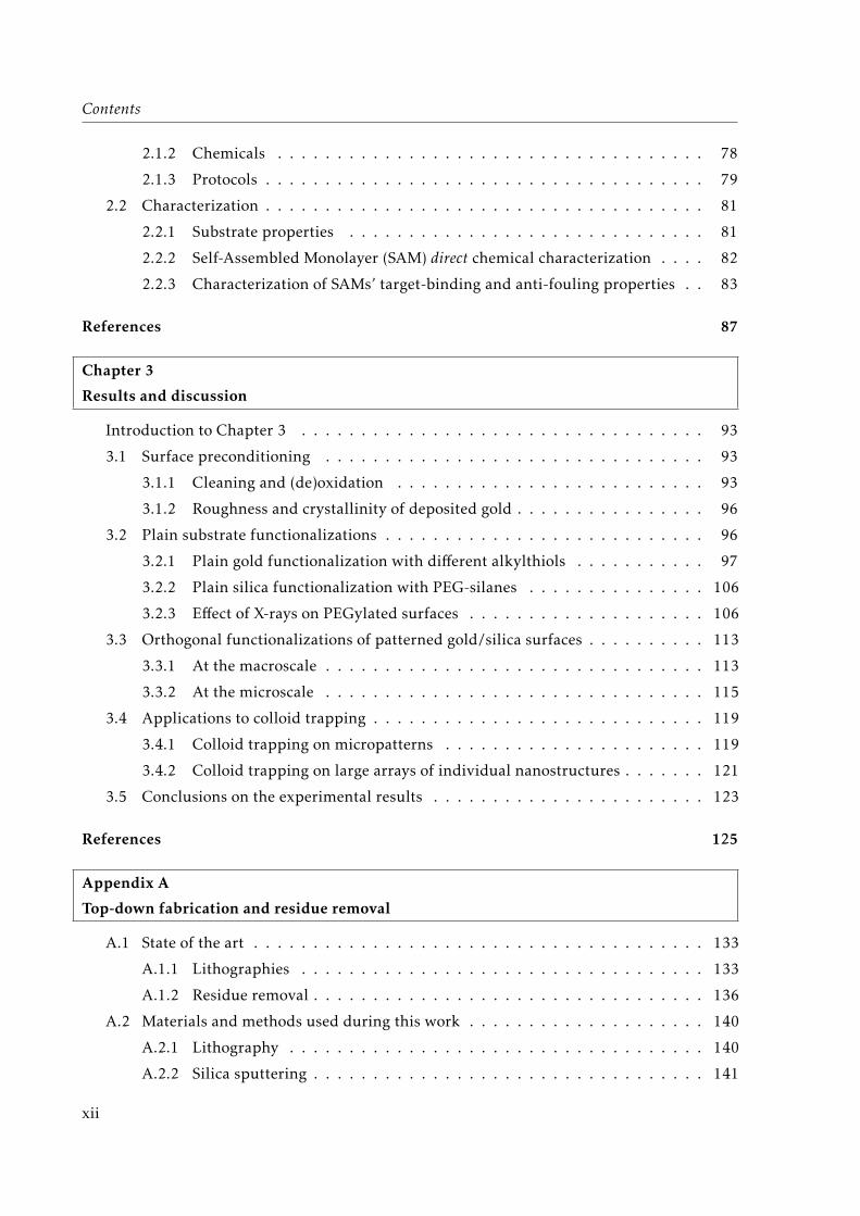
Le développement actuel des nanotechnologies implique de plus en plus des surfaces nano-structurées avec différents matériaux. Les biocapteurs plasmoniques, notamment, longtempsbasés sur l’exaltation de plasmons de surface (SPR, de l’anglais Surface Plasmon Resonance)propagatifs sur une couche mince métallique approchent leur limite de sensibilité1 qui resteen deça des performances nécessaires pour certaines applications (détection de traces de conta-minants ou marqueurs biologiques). De ce fait, ces capteurs sont en train de connaître actuel-lement le passage d’une structuration 1D (couche mince continue ; « SPR classique ») à desstructurations 2D et 3D avec des « points chauds » nanométriques provenant de l’excitation deplasmons localisées (LSPR ; voir Fig. 1).
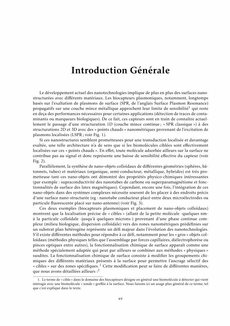
Si ces nanostructures semblent prometteuses pour une transduction localisée et davantageexaltée, une telle architecture n’a de sens que si les biomolécules ciblées sont effectivementlocalisées sur ces « points chauds ». En effet, toute molécule adsorbée ailleurs sur la surface necontribue pas au signal et donc représente une baisse de sensibilité effective du capteur (voirFig. 2).
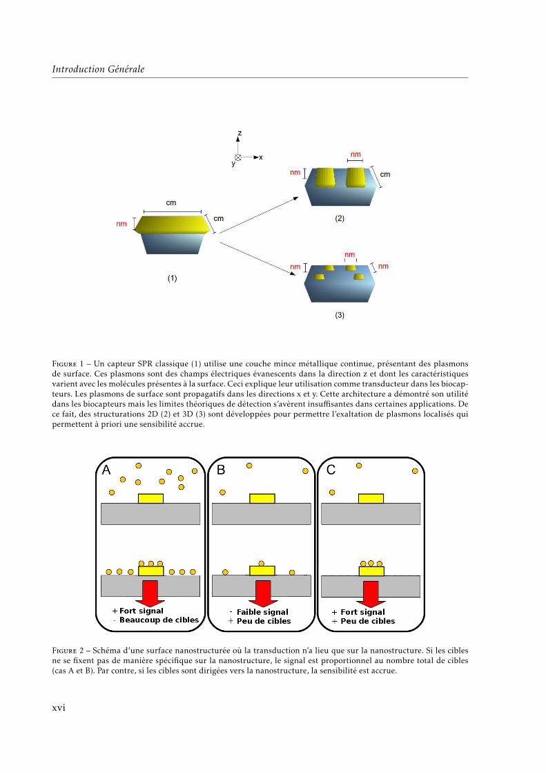
Parallèlement, la synthèse de nano-objets colloïdaux de différentes géométries (sphères, bâ-tonnets, tubes) et matériaux (organique, semi-conducteur, métallique, hybrides) est très pro-metteuse tant ces nano-objets ont démontré des propriétés physico-chimiques intéressantes(par exemple : supraconductivité des nanotubes de carbone ou superparamagnétisme et fonc-tionnalités de surface des latex magnétiques). Cependant, encore une fois, l’intégration de cesnano-objets dans des systèmes complexes nécessite souvent de les placer à des endroits précisd’une surface nano-structurée (eg : nanotube conducteur placé entre deux microélectrodes ouparticule fluorescente placé sur nano-antenne) (voir Fig. 3).
Ces deux exemples (biocapteurs plasmoniques et placement de nano-objets colloïdaux)montrent que la localisation précise de « cibles » (allant de la petite molécule -quelques nm-à la particule colloïdale -jusqu’à quelques microns-) provenant d’une phase continue com-plexe (milieu biologique, dispersion colloïdale) vers des zones nanométriques prédéfinies surun substrat plan hétérogène représente un défi majeur dans l’évolution des nanotechnologies.S’il existe différentes méthodes pour répondre à ce défi, notamment pour les « gros » objets col-loïdaux (méthodes physiques telles que l’assemblage par forces capillaires, diélectrophorèse oupinces optiques entre autres), la fonctionnalisation chimique de surface apparaît comme uneméthode spécialement adaptée qui peut par ailleurs se combiner aux méthodes « physiques »susdites. La fonctionnalisation chimique de surface consiste à modifier les groupements chi-miques des différents matériaux présents à la surface pour permettre l’ancrage sélectif des« cibles » sur des zones spécifiques. 1 Cette modification peut se faire de différentes manières,que nous avons détaillées ailleurs :2
1. Le terme de « cible » dans le domaine des biocapteurs désigne en général une biomolécule à détecter qui vientintéragir avec une biomolécule « sonde » greffée à la surface. Nous faisons ici un usage plus général de ce terme, telque c’est expliqué dans le texte.
xv
Introduction Générale
Figure 1 – Un capteur SPR classique (1) utilise une couche mince métallique continue, présentant des plasmonsde surface. Ces plasmons sont des champs électriques évanescents dans la direction z et dont les caractéristiquesvarient avec les molécules présentes à la surface. Ceci explique leur utilisation comme transducteur dans les biocap-teurs. Les plasmons de surface sont propagatifs dans les directions x et y. Cette architecture a démontré son utilitédans les biocapteurs mais les limites théoriques de détection s’avèrent insuffisantes dans certaines applications. Dece fait, des structurations 2D (2) et 3D (3) sont développées pour permettre l’exaltation de plasmons localisés quipermettent à priori une sensibilité accrue.
Figure 2 – Schéma d’une surface nanostructurée où la transduction n’a lieu que sur la nanostructure. Si les ciblesne se fixent pas de manière spécifique sur la nanostructure, le signal est proportionnel au nombre total de cibles(cas A et B). Par contre, si les cibles sont dirigées vers la nanostructure, la sensibilité est accrue.
xvi
Figure 3 – Localisation de nano-objets colloïdaux sur un système ayant une surface nano-structurée.2
1. En utilisant directement les groupements chimiques disponibles en surface (ex : sila-nols sur une surface de silice), modifiés par le biais d’un flux d’électrons ou d’ions parexemple.3
2. En adsorbant différents polymères ou autres macromolécules (« fonctionnalisation 3D »).4–6
3. En greffant de manière covalente des -petites- molécules dont une extrémité se lie ausubstrat et l’autre peut être choisie pour fixer ou repousser sélectivement une cible. Cesmolécules peuvent recouvrir plus ou moins la surface et acquérir une organisation plusou moins cristalline par interactions de Van der Waals entre les chaînes adjacentes. Danscertains cas (par exemple, alkylthiols sur Au(111) monocristallin) ces molécules formentune monocouche auto-assemblée (SAM, de l’anglais Self-Assembled Monolayer) avec uneorganisation pseudo-cristalline bien définie. 2
Cette troisième méthode présente certains avantages par rapport aux deux autres en termesde :
– Versatilité : l’extrémité disponible ou fonctionnelle peut être choisie parmi un grandnombre de groupements chimiques (théoriquement infini), contrairement à la premièreméthode qui est très limitée aux possibilités du substrat.
– Taille : Pour des applications biocapteurs à ondes évanescentes notamment, il peut êtreintéressant de limiter l’épaisseur de la couche d’accroche afin que la biomolécule à dé-tecter soit au plus près de la surface métallique, c’est à dire du maximum de champélectrique. De ce fait une monocouche moléculaire de quelques nanomètres peut êtrepréférable à l’emploi de polymères ou autres macromolécules de quelques dizaines denanomètres.
2. Le terme de SAM est souvent employé et pourra l’être dans le cours de ce manuscrit par simplicité ou abus delangage pour d’autres systèmes où les molécules ne forment pas forcément une monocouche et les degrès d’auto-assemblage sont probablement moindres (par exemple, poly(ethyelene glycol)-trialkoxysilanes sur silice amorphe).En outre, la relation entre l’organisation de la couche organique et sa réactivité est un sujet de recherche complexe.Nous ne l’aborderons pas en détail ici mais il convient de signaler que le cas « idéal » de la monocouche auto-assemblée parfaitement cristalline ne semble pas être forcément optimum pour la réactivité globale de la surface.
xvii
Introduction Générale
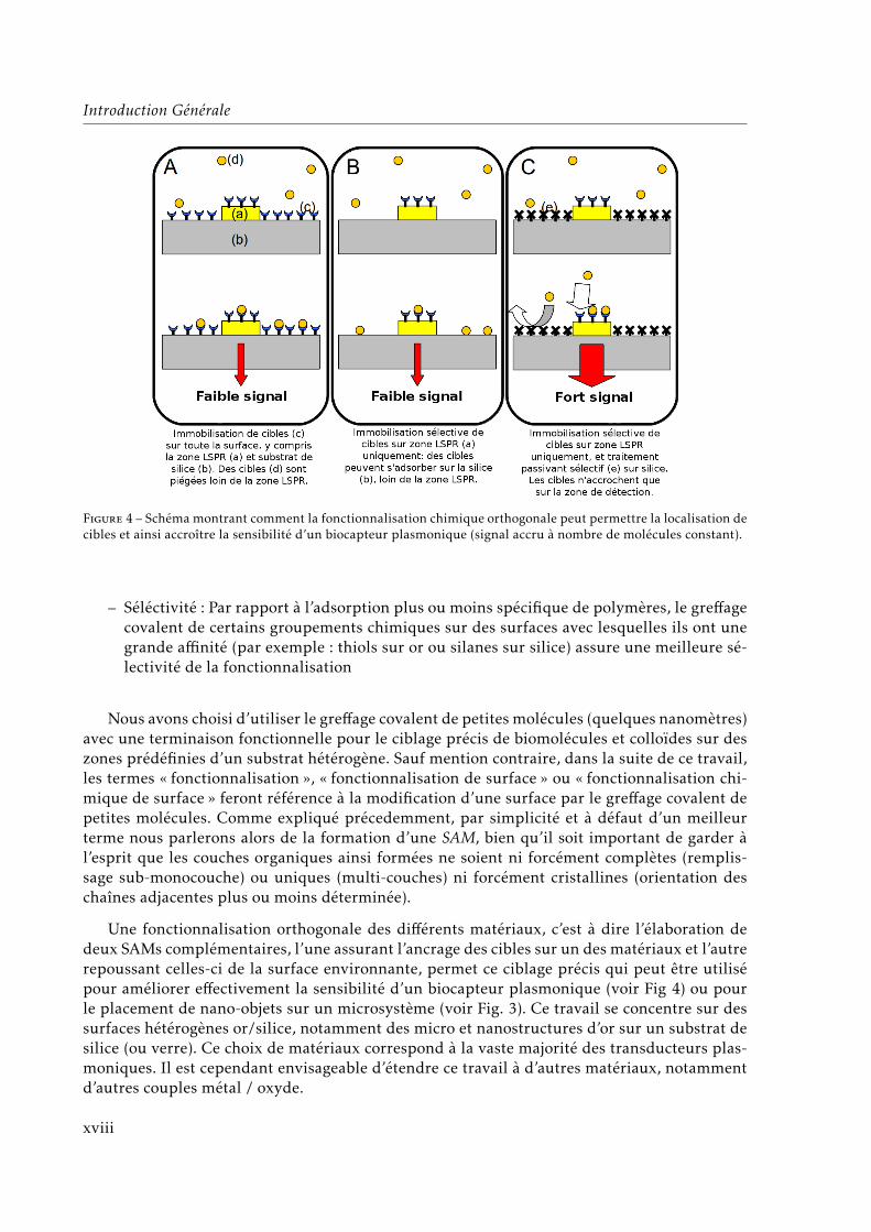
Figure 4 – Schéma montrant comment la fonctionnalisation chimique orthogonale peut permettre la localisation decibles et ainsi accroître la sensibilité d’un biocapteur plasmonique (signal accru à nombre de molécules constant).
– Séléctivité : Par rapport à l’adsorption plus ou moins spécifique de polymères, le greffagecovalent de certains groupements chimiques sur des surfaces avec lesquelles ils ont unegrande affinité (par exemple : thiols sur or ou silanes sur silice) assure une meilleure sé-lectivité de la fonctionnalisation
Nous avons choisi d’utiliser le greffage covalent de petites molécules (quelques nanomètres)avec une terminaison fonctionnelle pour le ciblage précis de biomolécules et colloïdes sur deszones prédéfinies d’un substrat hétérogène. Sauf mention contraire, dans la suite de ce travail,les termes « fonctionnalisation », « fonctionnalisation de surface » ou « fonctionnalisation chi-mique de surface » feront référence à la modification d’une surface par le greffage covalent depetites molécules. Comme expliqué précedemment, par simplicité et à défaut d’un meilleurterme nous parlerons alors de la formation d’une SAM, bien qu’il soit important de garder àl’esprit que les couches organiques ainsi formées ne soient ni forcément complètes (remplis-sage sub-monocouche) ou uniques (multi-couches) ni forcément cristallines (orientation deschaînes adjacentes plus ou moins déterminée).
Une fonctionnalisation orthogonale des différents matériaux, c’est à dire l’élaboration dedeux SAMs complémentaires, l’une assurant l’ancrage des cibles sur un des matériaux et l’autrerepoussant celles-ci de la surface environnante, permet ce ciblage précis qui peut être utilisépour améliorer effectivement la sensibilité d’un biocapteur plasmonique (voir Fig 4) ou pourle placement de nano-objets sur un microsystème (voir Fig. 3). Ce travail se concentre sur dessurfaces hétérogènes or/silice, notamment des micro et nanostructures d’or sur un substrat desilice (ou verre). Ce choix de matériaux correspond à la vaste majorité des transducteurs plas-moniques. Il est cependant envisageable d’étendre ce travail à d’autres matériaux, notammentd’autres couples métal / oxyde.
xviii

Ce manuscrit présente d’abord un état de l’art sur le sujet traitant d’une manière généralela question du ciblage sur surfaces planes hétérogènes par voies physiques et chimiques, puisplus précisément des fonctionnalisations d’or, de silice et de surfaces mixtes or/silice, avecune emphase particulière sur les méthodes de caractérisation chimique. Ensuite, l’ensembledes matériels et méthodes utilisés ont été regroupées dans un deuxième chapitre où le lec-teur pourra trouver précisément toutes les informations pour reproduire les résultats présentésdans le chapitre suivant. Ces résultats traiteront à la fois des questions plus fondamentales defonctionnalisation de surface sur or, sur silice et sur surfaces mixtes ainsi que des applicationsau placement de colloïdes et à la détection de biomolécules. Enfin, une conclusion généralepermettra de faire la synthèse de ces résultats et de les replacer dans le contexte scientifique ettechnologique actuel pour proposer différentes évolutions possibles.
xix

Introduction Générale
xx
General Introduction
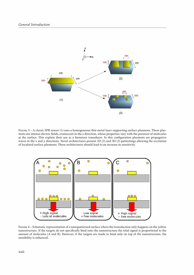
The current evolution of nanotechnology stresses the importance of patterned surfaces withdifferent materials. Plasmonic biosensors for instance, long based on the resonant excitation ofsurface plasmons (SPR) of a continuous metallic thin film are approaching their theoreticallimits of detection1 which remain too high for some practical applications. Thus, such sensorsare turning from a 1D structuration (homogeneous thin film ; “classic SPR”) to different 2D and3D patternings with nanometric “hot spots” emerging from the excitation of localized surfaceplasmons (LSRP ; see Fig. 5).
However, in order to take full advantage of such nanopatterned transducers, it is crucial toselectively place the target biomolecules onto the different “hot spots”. Otherwise, any targetmolecule adsorbed elsewhere will not contribute to the final signal and will thus skew theoverall sensitivity of the biosensor (see Fig. 6).
Simultaneously, nanofabrication has evolved into the synthesis of colloidal nano-objectswith different geometries (spheres, rods, tubes) and materials (organic, semi-conducting, me-tallic, hybrid). These nano-objects are very promising for their unprecedented physico-chemicalproperties (e.g : supraconductivity of carbon nanotubes -CNTs- or superparamagnetism andsurface functionalities of magnetic latexes). However, again, the integration of such nano-objects onto complex systems implies their precise placement onto a patterned surface (e.g :nanotube bridging two microelectrodes or fluorescent bead onto a plasmonic nano-antenna)(see Fig. 7).
These two examples (LSPR biosensors and localization of colloidal nano-objects) show howthe precise placement of “targets” (going from small molecules -few nanometers- to colloïds-up to few microns-) coming from a complex phase (biological medium, colloidal dispersion)onto predefined nanometric regions of a heterogeneous planar substrate constitutes a majorchallenge on the evolution of nanotechnology. There are different methods to answer this chal-lenge, specially for the bigger colloidal objects (physical methods such as capillary force assem-bly, dielectrophoresis or optical tweezers can be used). Nonetheless, surface chemical func-tionalization (which can be used in conjunction with the aforementioned physical methods)appears as a specially appropriate manner to overcome this technological bottleneck. Surfacechemical functionalization consists in modifying the chemical surface groups of different ma-terials to allow the selective binding of “targets” onto specific regions. 3 Such modification canbe done in several ways that we have detailed elsewhere :2
1. Chemical groups present at the surface (e.g : silanols on a silica surface) can be readilymodified by an electron or ion beam.3
3. The term “target” is used in the field of biosensors to designate at biomolecule that needs to be detected, thisbiomolecule interacting with a “probe” biomolecule grafted on the surface. We make a more general use of thisterm here, as explained in the text.
xxi
General Introduction
Figure 5 – A classic SPR sensor (1) uses a homogeneous thin metal layer supporting surface plasmons. These plas-mons are intense electric fields, evanescent in the z direction, whose properties vary with the presence of moleculesat the surface. This explain their use as a biosensor transducer. In this configuration plasmons are propagativewaves in the x and y directions. Novel architectures present 2D (2) and 3D (3) patternings allowing the excitationof localized surface plasmons. These architectures should lead to an increase in sensitivity.
Figure 6 – Schematic representation of a nanopatterned surface where the transduction only happens on the yellownanostructure. If the targets do not specifically bind onto the nanostructure the total signal is proportional to theamount of molecules (A and B). However, if the targets are made to bind only on top of the nanostructure, thesensibility is enhanced.
xxii
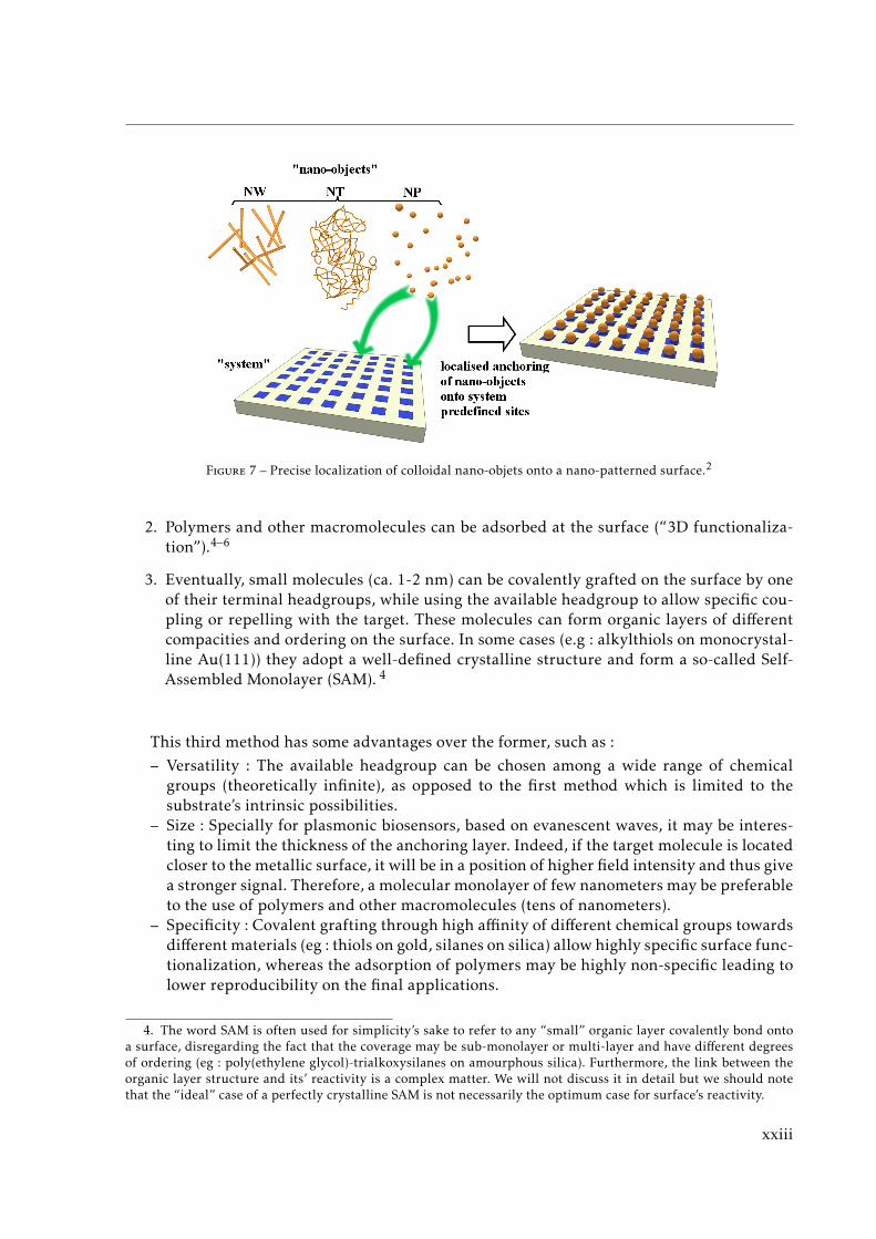
Figure 7 – Precise localization of colloidal nano-objets onto a nano-patterned surface.2
2. Polymers and other macromolecules can be adsorbed at the surface (“3D functionaliza-tion”).4–6
3. Eventually, small molecules (ca. 1-2 nm) can be covalently grafted on the surface by oneof their terminal headgroups, while using the available headgroup to allow specific cou-pling or repelling with the target. These molecules can form organic layers of differentcompacities and ordering on the surface. In some cases (e.g : alkylthiols on monocrystal-line Au(111)) they adopt a well-defined crystalline structure and form a so-called Self-Assembled Monolayer (SAM). 4
This third method has some advantages over the former, such as :– Versatility : The available headgroup can be chosen among a wide range of chemical
groups (theoretically infinite), as opposed to the first method which is limited to thesubstrate’s intrinsic possibilities.
– Size : Specially for plasmonic biosensors, based on evanescent waves, it may be interes-ting to limit the thickness of the anchoring layer. Indeed, if the target molecule is locatedcloser to the metallic surface, it will be in a position of higher field intensity and thus givea stronger signal. Therefore, a molecular monolayer of few nanometers may be preferableto the use of polymers and other macromolecules (tens of nanometers).
– Specificity : Covalent grafting through high affinity of different chemical groups towardsdifferent materials (eg : thiols on gold, silanes on silica) allow highly specific surface func-tionalization, whereas the adsorption of polymers may be highly non-specific leading tolower reproducibility on the final applications.
4. The word SAM is often used for simplicity’s sake to refer to any “small” organic layer covalently bond ontoa surface, disregarding the fact that the coverage may be sub-monolayer or multi-layer and have different degreesof ordering (eg : poly(ethylene glycol)-trialkoxysilanes on amourphous silica). Furthermore, the link between theorganic layer structure and its’ reactivity is a complex matter. We will not discuss it in detail but we should notethat the “ideal” case of a perfectly crystalline SAM is not necessarily the optimum case for surface’s reactivity.
xxiii
General Introduction
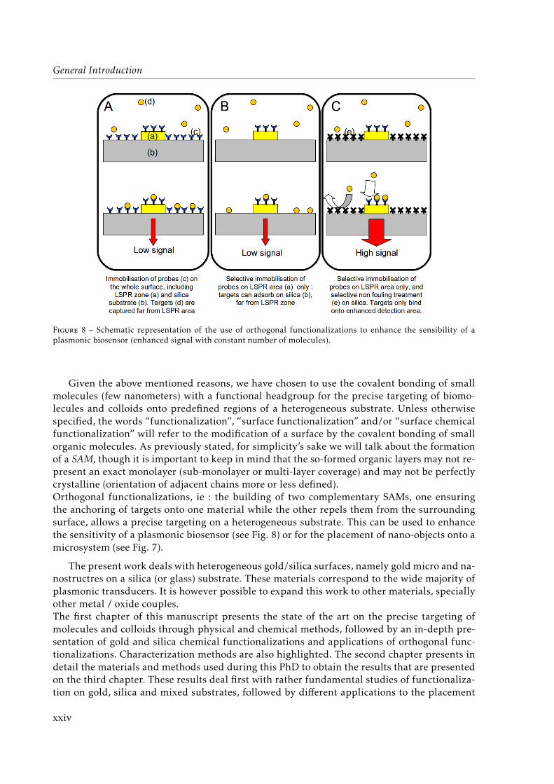
Figure 8 – Schematic representation of the use of orthogonal functionalizations to enhance the sensibility of aplasmonic biosensor (enhanced signal with constant number of molecules).
Given the above mentioned reasons, we have chosen to use the covalent bonding of smallmolecules (few nanometers) with a functional headgroup for the precise targeting of biomo-lecules and colloids onto predefined regions of a heterogeneous substrate. Unless otherwisespecified, the words “functionalization”, “surface functionalization” and/or “surface chemicalfunctionalization” will refer to the modification of a surface by the covalent bonding of smallorganic molecules. As previously stated, for simplicity’s sake we will talk about the formationof a SAM, though it is important to keep in mind that the so-formed organic layers may not re-present an exact monolayer (sub-monolayer or multi-layer coverage) and may not be perfectlycrystalline (orientation of adjacent chains more or less defined).Orthogonal functionalizations, ie : the building of two complementary SAMs, one ensuringthe anchoring of targets onto one material while the other repels them from the surroundingsurface, allows a precise targeting on a heterogeneous substrate. This can be used to enhancethe sensitivity of a plasmonic biosensor (see Fig. 8) or for the placement of nano-objects onto amicrosystem (see Fig. 7).
The present work deals with heterogeneous gold/silica surfaces, namely gold micro and na-nostructres on a silica (or glass) substrate. These materials correspond to the wide majority ofplasmonic transducers. It is however possible to expand this work to other materials, speciallyother metal / oxide couples.The first chapter of this manuscript presents the state of the art on the precise targeting ofmolecules and colloids through physical and chemical methods, followed by an in-depth pre-sentation of gold and silica chemical functionalizations and applications of orthogonal func-tionalizations. Characterization methods are also highlighted. The second chapter presents indetail the materials and methods used during this PhD to obtain the results that are presentedon the third chapter. These results deal first with rather fundamental studies of functionaliza-tion on gold, silica and mixed substrates, followed by different applications to the placement
xxiv

of colloids and biomolecules detection. Eventually, a general conclusion is given to summarizethe obtained results and place them in today’s scientifical and technological context to suggestdifferent possible evolutions.
xxv

General Introduction
xxvi
References
[1] M. Piliarik and J. Homola. Optics express, 17,16505–16517 (2009).
[2] F. Palazon, P. Rojo Romeo, A. Belarouci, C. Chevalier, H. Chamas, E. Souteyrand, A. Souifi,Y. Chevolot, and J.-P. Cloarec. Site-selective self-assembly of nano-objects on a planar sub-strate based on surface chemical functionalization. In C. Joachim, editor, Advances in Atomand Single Molecule Machines. Springer (in press) (2014).
[3] M. Kolibal, M. Konecny, F. Ligmajer, D. Skoda, T. Vystavel, J. Zlamal, P. Varga, and T. Sikola.ACS nano, 6,10098–10106 (2012).
[4] L. Feuz, P. Jönsson, M. P. Jonsson, and F. Höök. ACS nano, 4,2167–77 (2010).
[5] K. Kumar, A. B. Dahlin, T. Sannomiya, S. Kaufmann, L. Isa, and E. Reimhult. Nano letters,13,6122–6129 (2013).
[6] L. Feuz, M. P. Jonsson, and F. Höök. Nano letters, 12,873–9 (2012).
xxvii

References
xxviii
Liste of Tables
1.1 Different types of objects considered in this chapter. . . . . . . . . . . . . . . . . 121.2 Main limitations of the different trapping methods. . . . . . . . . . . . . . . . . . 211.3 Different gold-binding headgroups. . . . . . . . . . . . . . . . . . . . . . . . . . . 271.4 Reported functional headgroups of SAMs on gold substrates. . . . . . . . . . . . 321.5 Different combinations of thiolate mixed-SAMs reported in the literature. . . . . 331.6 Summary of different surface chemistry characterization tools. . . . . . . . . . . 47
3.1 Atomic percentages of oxygen, carbon and gold on PEGylated gold surfaces be-fore and after 9h irradiation, determined by X-ray Photoelectron Spectroscopy(XPS). . . . . . . . . . . . . . . . . . . . . . . . . . . . . . . . . . . . . . . . . . . . 108
A.1 UV and e-beam lithographies . . . . . . . . . . . . . . . . . . . . . . . . . . . . . 136A.2 Wet processes for surface cleaning (removal of organic residues after lithography).138A.3 Dry processes for surface cleaning (removal of organic residues after lithography).139
xxix

Liste of Tables
xxx
List of Figures
1 Un capteur SPR classique (1) utilise une couche mince métallique continue, pré-sentant des plasmons de surface. Ces plasmons sont des champs électriques éva-nescents dans la direction z et dont les caractéristiques varient avec les moléculesprésentes à la surface. Ceci explique leur utilisation comme transducteur dansles biocapteurs. Les plasmons de surface sont propagatifs dans les directions xet y. Cette architecture a démontré son utilité dans les biocapteurs mais les li-mites théoriques de détection s’avèrent insuffisantes dans certaines applications.De ce fait, des structurations 2D (2) et 3D (3) sont développées pour permettrel’exaltation de plasmons localisés qui permettent à priori une sensibilité accrue. xvi
2 Schéma d’une surface nanostructurée où la transduction n’a lieu que sur la na-nostructure. Si les cibles ne se fixent pas de manière spécifique sur la nanostruc-ture, le signal est proportionnel au nombre total de cibles (cas A et B). Par contre,si les cibles sont dirigées vers la nanostructure, la sensibilité est accrue. . . . . . xvi
3 Localisation de nano-objets colloïdaux sur un système ayant une surface nano-structurée. . . . . . . . . . . . . . . . . . . . . . . . . . . . . . . . . . . . . . . . . xvii
4 Schéma montrant comment la fonctionnalisation chimique orthogonale peut per-mettre la localisation de cibles et ainsi accroître la sensibilité d’un biocapteurplasmonique (signal accru à nombre de molécules constant). . . . . . . . . . . . xviii
5 A classic SPR sensor (1) uses a homogeneous thin metal layer supporting sur-face plasmons. These plasmons are intense electric fields, evanescent in the zdirection, whose properties vary with the presence of molecules at the surface.This explain their use as a biosensor transducer. In this configuration plasmonsare propagative waves in the x and y directions. Novel architectures present 2D(2) and 3D (3) patternings allowing the excitation of localized surface plasmons.These architectures should lead to an increase in sensitivity. . . . . . . . . . . . . xxii
6 Schematic representation of a nanopatterned surface where the transductiononly happens on the yellow nanostructure. If the targets do not specifically bindonto the nanostructure the total signal is proportional to the amount of mole-cules (A and B). However, if the targets are made to bind only on top of thenanostructure, the sensibility is enhanced. . . . . . . . . . . . . . . . . . . . . . . xxii
7 Precise localization of colloidal nano-objets onto a nano-patterned surface. . . . xxiii8 Schematic representation of the use of orthogonal functionalizations to enhance
the sensibility of a plasmonic biosensor (enhanced signal with constant numberof molecules). . . . . . . . . . . . . . . . . . . . . . . . . . . . . . . . . . . . . . . xxiv
1.1 Different fluidic approaches for Capillary Force Assembly (CFA). . . . . . . . . . 13
xxxi

List of Figures
1.2 Schematic representation of the localized deposition of nanoparticles throughe-beam lithography, CFA and lift-off. . . . . . . . . . . . . . . . . . . . . . . . . . 14
1.3 Trap density vs particle size using CFA. . . . . . . . . . . . . . . . . . . . . . . . 141.4 Efficiency of parallel DEP trapping of single nanowires. . . . . . . . . . . . . . . 171.5 Efficiency of parallel DEP trapping of CNTs. . . . . . . . . . . . . . . . . . . . . . 181.6 Plasmonic array traps for spherical particles. . . . . . . . . . . . . . . . . . . . . 191.7 Magnetic array traps for spherical particles. . . . . . . . . . . . . . . . . . . . . . 191.8 Comparison of different methods for parallel trapping of spherical particles. . . 211.9 Schematic representation of surface functionalization and its use for particle
trapping. . . . . . . . . . . . . . . . . . . . . . . . . . . . . . . . . . . . . . . . . . 221.10 Ideal representation of self-assembled monolayers on a solid surface. . . . . . . . 231.11 Odd-Even effect. . . . . . . . . . . . . . . . . . . . . . . . . . . . . . . . . . . . . . 291.12 Micro-contact printing. . . . . . . . . . . . . . . . . . . . . . . . . . . . . . . . . . 351.13 Schematic representation of binding energies of thiols and thiolates on gold. . . 381.14 Structural model of the commensurate adlayer formed by thiols on the gold lattice. 391.15 Tilt, twist and precession angles of alkanethiolates on gold. . . . . . . . . . . . . 391.16 Schematic illustration of some of the intrinsic and extrinsic defects found in
SAMs formed on polycrystalline substrates. . . . . . . . . . . . . . . . . . . . . . 401.17 Schematic representation of samples’ dimensions (not to scale). . . . . . . . . . . 52
3.1 XPS spectra of silica surfaces exposed to Poly(methyl methacrylate) (PMMA) andcleaned with different procedures. . . . . . . . . . . . . . . . . . . . . . . . . . . . 94
3.2 Au4f XPS spectra of a gold sample right after undergoing oxygen plasma clea-ning and 12h later. . . . . . . . . . . . . . . . . . . . . . . . . . . . . . . . . . . . 95
3.3 Gold surface roughness (a) and crystallinity (b) . . . . . . . . . . . . . . . . . . . 963.4 Polarization-Modulation InfraRed Reflection Absorbtion Spectroscopy (PM-IRRAS)
spectra of HS-(CH2)11-NH-C(O)-Biotin (MU-Biot), 11-amino-undecanethiol hydro-chloride (MUAM) and 11-mercapto-1-undecanoic acid (MUA) SAMs on gold.The most relevant infrared peaks of each molecules can be clearly identifiedon the corresponding spectrum, showing the success of the chemical functiona-lizations. . . . . . . . . . . . . . . . . . . . . . . . . . . . . . . . . . . . . . . . . . 97
3.5 Samples activated in (a) water and (b) TetraHydroFuran (THF) with 100 mMconcentrations of corresponding carbodiimide and N-hydroxysuccinimide (NHS).Characteristic NHS absorption wavenumbers are written in bold and 1818cm−1
peak, characteristic of NHS-ester is written in bold and italics. . . . . . . . . . . 1013.6 Area of the 1818cm−1 peak for different solvents/carbodiimides, concentrations
and times. Below a value of 150 a.u. the peak is barely noticeable. . . . . . . . . 1023.7 Negative ((a) and (b)) mode and positive ((c) and (d)) mode Time-of-Flight Se-
condary Ion Mass Spectroscopy (ToF-SIMS) spectra of samples activated in water((a) and (c)) and THF ((b) and (d)) after 24h, in the range of m/z=5-120 (negativemode) and m/z=0-100 (positive mode). . . . . . . . . . . . . . . . . . . . . . . . . 104
3.8 C1s XPS spectrum of PEGylated silica surface. Because of the degradation ofsuch molecule under irradiation a single scan is presented instead of the usualco-addition of several scans which, in the absence of degradation, would yield abetter signal-to-noise ratio. . . . . . . . . . . . . . . . . . . . . . . . . . . . . . . . 106
3.9 Evolution of the C1s spectra of PEGylated silica. Left image shows a map of thespectrum over time. The time between two scans is ca. 3.6 minutes. Right imageshows 4 spectra in detail at selected times. . . . . . . . . . . . . . . . . . . . . . . 107
xxxii
3.10 Evolution of the C1s spectra of PEGylated gold. Left image shows a map of thespectrum over time. The time between two scans is ca. 9 minutes. Right imageshows 4 spectra in detail at selected times. . . . . . . . . . . . . . . . . . . . . . . 108
3.11 Evolution (map) of the O1s (a) and Au4f (b) spectra of PEGylated gold over timeof continuous irradiation. The time between two scans is ca. 9 minutes. . . . . . 108
3.12 Relative contributions of Oligo(Ethylene Glycol) (OEG) (CO peak) to the totalC1s amount. On silica, the low intensity of peaks after 4h makes it difficult tofit both contributions. On gold, the normalized CO intensity continues to decaylinearly reaching a value of under 0.3 after 9h (not shown here). . . . . . . . . . 109
3.13 PM-IRRAS spectra of a PEGylated gold sample before and after 18 hours X-Rayirradiation by continuous XPS measurements. . . . . . . . . . . . . . . . . . . . . 110
3.14 Spectra of PEGylated silica surface at t=0 and t=18 hours, without irradiationbetween the two measurements. . . . . . . . . . . . . . . . . . . . . . . . . . . . . 110
3.15 Fluorescence intensities after adsorption of fluorescently-labeled streptavidin onan irradiated and non-irradiated sample. A 12mm2 area was scanned at 3µm re-solution with fluorescence intensities converted to 8 bits and values binned by 2(128 bins). Non-irradiated sample shows a very low fluorescence (average inten-sity around 7) compared to the irradiated sample (average around 100) whichtranslates a much higher amount of protein adsorption on the irradiated sample. 111
3.16 Evolution of the C1s (a) and O1s (b) peaks positions of PEGylated gold over timeof continuous irradiation. . . . . . . . . . . . . . . . . . . . . . . . . . . . . . . . . 112
3.17 XPS C1s spectra on the gold and silica regions of an heterogeneous sample or-thogonally functionalized with MUA and 2-[methoxy(polyethyleneoxy)propyl]-trimethoxysilane (MW=460 g/mol; i.e., 6 ethyleneglycol units in average) (PEG-Si). . . . . . . . . . . . . . . . . . . . . . . . . . . . . . . . . . . . . . . . . . . . . . 114
3.18 XPS image of a micropatterned orthogonally functionalized (1H,1H,2H,2H-Per-fluorodecanethiol (AuF) + PEG-Si) gold on silica substrate. . . . . . . . . . . . . 116
3.19 XPS image of a micropatterned orthogonally functionalized (MUA + Trichloro-(1H,1H,2H,2H-perfluorooctyl)silane (SiF)) gold on silica substrate. . . . . . . . . 117
3.20 [XPS Au4f and F1s mapping of micropatterned gold on silica surface orthogo-nally functionalized with AuF and PEG-Si.]XPS Au4f (a) and F1s (b) mapping ofmicropatterned gold on silica surface orthogonally functionalized with AuF andPEG-Si. Fluorine is only and homogeneously found in the same regions as gold,demonstrating the good orthogonality of the functionalizations. . . . . . . . . . 118
3.21 XPS Au4f and F1s mapping of micropatterned gold on silica surface orthogo-nally functionalized with SiF and MUA. . . . . . . . . . . . . . . . . . . . . . . . 118
3.22 ToF-SIMS fluorine mapping of orthogonally functionalized patterned gold onsilica surfaces . . . . . . . . . . . . . . . . . . . . . . . . . . . . . . . . . . . . . . 118
3.23 Schematic representation of the bio-affinity and electrostatic approaches to theselective anchoring of different nanoparticles. . . . . . . . . . . . . . . . . . . . . 119
3.24 Scanning Electron Microscopy (SEM) images of patterned functionalized samplesafter colloid deposition. The gold structures (lines, squares) appear brighter thanthe surrounding silica. Colloidal particles can be seen on the surface, with a pre-ferential deposition on the gold regions. Images (a) and (c) are taken on bio-affinity based samples while (b) and (d) are taken on electrostatic based samples. 120
xxxiii
List of Figures
3.25 Histogram presenting the surface coverage by latex nanoparticles on gold and si-lica regions of differently functionalized samples: “Ref” refers to a non-functionalizedsurface; “Bio” refers to a biotinylated surface (streptavidin-functionalized beads)and “Elec” to an amino-functionalized surface (carboxylatex beads). Differentcolumns correspond to different samples and error bars represent the measuredstandard deviation between three regions of the same sample. . . . . . . . . . . . 120
3.26 3x4 array of dimer nano-antennas with fluorescent nanobeads attached throughsurface chemical functionalization. 11 out of 12 nano-antennas (green circles)are occupied by one, two or three nanobeads, preferentially anchored at theedges and corners. Only one nano-antenna is found unoccupied (red circle) whilelow non-specific adsorption (yellow circles) is found on the surrounding silica. . 122
3.27 SEM images of single dimer nano-antennas with trapped nanobeads . . . . . . . 123
A.1 Simplified lithography principle. . . . . . . . . . . . . . . . . . . . . . . . . . . . 134
B.1 Electric double layer and corresponding potential for a negatively charged surface.144B.2 Derjaguin, Landau, Verwey, Overbeek (DLVO) energy vs separation distance.
EDL stands for electrical double layer repulsion, VdW stands for Van der Waalsattractive interaction and DLVO is the sum of both contributions. . . . . . . . . . 145
C.1 Schematic representation of IR absorbtion bands (source: wikipedia). . . . . . . 147C.2 Contact angle principle (source: wikipedia). . . . . . . . . . . . . . . . . . . . . . 152C.3 Atomic force microscopy (source: wikipedia). . . . . . . . . . . . . . . . . . . . . 153C.4 X-Ray Diffraction (source: wikipedia). . . . . . . . . . . . . . . . . . . . . . . . . . 154
xxxiv
Glossary
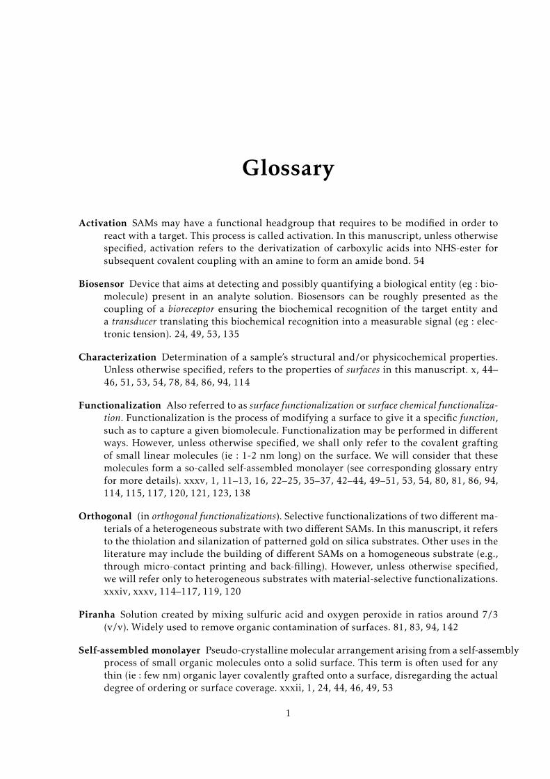
Activation SAMs may have a functional headgroup that requires to be modified in order toreact with a target. This process is called activation. In this manuscript, unless otherwisespecified, activation refers to the derivatization of carboxylic acids into NHS-ester forsubsequent covalent coupling with an amine to form an amide bond. 54
Biosensor Device that aims at detecting and possibly quantifying a biological entity (eg : bio-molecule) present in an analyte solution. Biosensors can be roughly presented as thecoupling of a bioreceptor ensuring the biochemical recognition of the target entity anda transducer translating this biochemical recognition into a measurable signal (eg : elec-tronic tension). 24, 49, 53, 135
Characterization Determination of a sample’s structural and/or physicochemical properties.Unless otherwise specified, refers to the properties of surfaces in this manuscript. x, 44–46, 51, 53, 54, 78, 84, 86, 94, 114
Functionalization Also referred to as surface functionalization or surface chemical functionaliza-tion. Functionalization is the process of modifying a surface to give it a specific function,such as to capture a given biomolecule. Functionalization may be performed in differentways. However, unless otherwise specified, we shall only refer to the covalent graftingof small linear molecules (ie : 1-2 nm long) on the surface. We will consider that thesemolecules form a so-called self-assembled monolayer (see corresponding glossary entryfor more details). xxxv, 1, 11–13, 16, 22–25, 35–37, 42–44, 49–51, 53, 54, 80, 81, 86, 94,114, 115, 117, 120, 121, 123, 138
Orthogonal (in orthogonal functionalizations). Selective functionalizations of two different ma-terials of a heterogeneous substrate with two different SAMs. In this manuscript, it refersto the thiolation and silanization of patterned gold on silica substrates. Other uses in theliterature may include the building of different SAMs on a homogeneous substrate (e.g.,through micro-contact printing and back-filling). However, unless otherwise specified,we will refer only to heterogeneous substrates with material-selective functionalizations.xxxiv, xxxv, 114–117, 119, 120
Piranha Solution created by mixing sulfuric acid and oxygen peroxide in ratios around 7/3(v/v). Widely used to remove organic contamination of surfaces. 81, 83, 94, 142
Self-assembled monolayer Pseudo-crystalline molecular arrangement arising from a self-assemblyprocess of small organic molecules onto a solid surface. This term is often used for anythin (ie : few nm) organic layer covalently grafted onto a surface, disregarding the actualdegree of ordering or surface coverage. xxxii, 1, 24, 44, 46, 49, 53
1
Glossary
Substrate Solid surface onto which something is deposited. In this manuscript, this term refersto the surface onto which SAMs are formed. Thus, if we consider a silicon wafer witha deposited thin film of gold with a chromium interlayer, we shall speak about a goldsubstrate for the formation of an alkanethiolate SAM. This may depart from the classicalmicrofabrication point-of-view which would consider the silicon wafer as the substratein this case. xxxii, 1, 12, 13, 15, 16, 19, 21–24, 42, 49, 51, 53, 54, 80, 81, 86, 94, 98, 114,117, 121, 123, 135, 136, 138
Target Colloidal object or single biomolecule that has to be specifically anchored at givenregions (traps) of a surface. This may depart from the more restrictive classical biosensorpoint-of-view in which targets are biomolecules (e.g., antigen) which are recognized byother probe biomolecules (e.g., antibody). x, 1, 2, 22, 24, 29, 30, 53–55, 78, 86
Trap Specific predefined region of a solid surface where a target is expected to be anchored.These regions may differ from the surrounding surface by their topography and/or che-mical composition. xxix, xxxii, xxxv, 2, 13–23, 53, 86, 87, 94, 121, 123, 125
2
Acronyms
AFM Atomic Force Microscopy. xi, 42, 47, 48, 54, 55, 78, 83, 84, 98, 154, 156
AUF 1H,1H,2H,2H-Perfluorodecanethiol. xxxv, 80, 82, 117, 119, 120
BOE Buffered Oxide Etch. 139
C-AFM Conductive Atomic Force Microscopy. 47
CFA Capillary Force Assembly. xxxii, 13, 14, 22
CFM Chemical Force Microscopy. 47, 156
CNT Carbon Nanotube. 12, 16
CTAB Cationic hexadecylTrimethyl Ammonium Bromide. 139
CV Cyclic Voltametry. 45
DCC N,N’-DiCyclohexylCarbodiimide. 99
DCE DiChloroEthane. 139
DCM DiChloroMethane. 35, 81–83, 115, 139, 143, 144
DEP Dielectrophoresis. 16, 17, 19
DIC Diisopropylcarbodiimide. 81, 83, 99, 103, 107
DLVO Derjaguin, Landau, Verwey, Overbeek. xi, xxxv, 12, 123, 145, 147
DMF DiMethylFormamide. 35
DMSO DiMethyl SulfOxide. 99
DNA DeoxyriboNucleic Acid. 49, 50, 99
DNQ DiazoNaphthoQuinone. 136, 138
EDC 1-Ethyl-3-(3-Dimethylaminopropyl)Carbodiimide hydrochloride. xxix, 33, 81, 83, 99, 103,105
EG Ethylene Glycol. 37
EG3-COOH HS-(CH2)11-EG3-COOH. 80
EG3-OME HS-(CH2)11-EG3-OCH3. 80
EG6-COOH HS-(CH2)11-EG6-COOH. 81
EG6-OME HS-(CH2)11-EG6-OCH3. 80
EIS Electrochemical Impedance Spectroscopy. 45
ESCA Electron Spectroscopy for Chemical Analysis. 46
3
Acronyms
FTIR Fourier-Transform Infrared Spectrosocpy. xi, 84, 149, 150
GAE4E Glycolic Acid Ethoxylate 4-tert-butylphenyl Ether. 139
HMDS Hexamethyldisilazane. 140, 141, 143
HSQ Hydrogen SilsesQuioxane. 136, 138
IEF Institut d’Électronique Fondamentale. 142, 143
INL Institut des Nanotechnologies de Lyon. 84, 142, 143
IPA IsoproPAnol. 139, 143
IR Infrared. 45, 46, 48, 149
IRRAS Infrared Reflection Absorption Spectroscopy. 84, 149, 150
ISA Institut des Sciences Analytiques. 84, 117
LSPR Localized Surface Plasmon Resonance. 49–51, 54, 55, 123
LTDS Laboratoire de Tribologie et Dynamique des Surfaces. 84, 117
MFM Magnetic Force Microscopy. 47
MIBK Methyl isobutyl ketone. 136, 138, 143
MIF Metal-Ion Free. 143
MMA Methyl methacrylate. 143
MUA 11-mercapto-1-undecanoic acid. xxxiii–xxxv, 35, 49, 54, 80–82, 94, 98, 100, 103, 115–117, 120
MUAM 11-amino-undecanethiol hydrochloride. xxxiii, 80, 81, 87, 100, 121, 123
MU-BIOT HS-(CH2)11-NH-C(O)-Biotin. xxxiii, 54, 80, 81, 100, 121
MUOH 11-mercapto-1-undecanol. 35, 80, 81
MWCNT Multi-Wall Carbon Nanotube. 16
NHS N-hydroxysuccinimide. xxxiii, 1, 54, 81, 83, 94, 98, 99, 102–105, 107
NMP N-Methyl Pyrrolidone. 139
OEG Oligo(Ethylene Glycol). xxix, xxxiv, 29, 49, 107, 108, 110–112, 114
PBS Phosphate Buffered Saline. 86, 87, 99, 123, 148
PDMS Poly(dimethyl siloxane). 36
PEG Poly(Ethylene Glycol). xxxiv, 24, 29, 30, 34, 37, 42, 46, 49–51, 54, 81, 82, 94, 108, 111,116, 117
PEG-SI 2-[methoxy(polyethyleneoxy)propyl]trimethoxysilane (MW=460 g/mol ; i.e., 6 ethy-leneglycol units in average). xxxiv, xxxv, 54, 81, 82, 107, 115–117, 119, 120
PEM PhotoElastic Modulator. 84, 85, 150–152
PFM Piezoelectric Force Microscopy. 47
PLL Poly-L-Lysine. 50, 51
4
Acronyms
PM-IRRAS Polarization-Modulation InfraRed Reflection Absorbtion Spectroscopy. xi, xxxiii,xxxiv, 35, 46, 54, 78, 84, 99, 100, 103, 105, 108, 111, 113–115, 121, 149–151
PMMA Poly(methyl methacrylate). 94, 136, 138, 139, 142, 143
PMT PhotoMultiplier Tube. 88
POE Poly(OxyEthylene). 108
PTFE PolyTetraFluoroEthylene. 108
PVC Poly(Vinyl Chloride). 108
PVDF PolyVinyliDene Fluoride. 108
QCM Quartz Crystal Microbalance. 44, 143, 144
RIE Reactive Ion Etching. 94
RMS Root Mean Square. 98
RNA RiboNucleic Acid. 99
SAM Self-Assembled Monolayer. x, xxix, xxxii, xxxiii, 1, 2, 10, 24, 25, 29, 30, 33–39, 41–47, 49,50, 54, 78, 81, 83, 84, 86, 94, 98–100, 103, 156
SEM Scanning Electron Microscopy. xi, xxxv, 51, 54, 55, 86, 87, 117, 121, 122, 125, 136, 157
SERS Surface-Enhanced Raman Spectroscopy. 46
SET Single Electron Transistor. 50
SIF Trichloro(1H,1H,2H,2H-perfluorooctyl)silane. xxxv, 54, 81, 82, 117, 120
SPR Surface Plasmon Resonance. 44, 51, 55
STEM Scanning Transmission Electron Microscope or Microscopy. 138
STM Scanning Tunnelling Microscopy. 47, 48
SWCNT Single-Wall Carbon Nanotube. 16
TASA Template-Assisted Self Assembly. 13
TERS Tip-Enhanced Raman Spectroscopy. 46–48
THF TetraHydroFuran. xxxiii, 35, 81, 83, 99, 103–107
TMAH TetraMethylAmmonium Hydroxide. 136, 138, 140, 143
TOF-SIMS Time-of-Flight Secondary Ion Mass Spectroscopy. xi, xxxiii, xxxv, 46, 48, 54, 55,78, 84, 85, 99, 103, 105, 106, 114, 117, 120, 153
UDT Undecanethiol. 80, 81
UHV Ultrahigh Vacuum. 37, 42
UV Ultraviolet. 54, 94, 108, 117, 135, 136, 138, 143
XPS X-ray Photoelectron Spectroscopy. xi, xxix, xxxiii, xxxiv, 35, 45, 46, 48, 54, 55, 78, 80,84–86, 94, 95, 97, 99, 107, 108, 110–115, 117, 120, 144, 152, 153
XRD X-Ray Diffraction. xi, 78, 83, 84, 98, 156, 157
YAG Yttrium Aluminium Garnet, Y3Al5O12. 141
5

Acronyms
6

Chapter 1
State of the art
7

Chapter 1. State of the art
Résumé du Chapitre 1
Pour répondre à la problématique posée dans cette thèse, à savoir : Comment positionnerprécisément un ensemble de biomolécules ou de colloïdes provenant d’un milieu complexe sur unepluralité de régions micro et nanométriques prédéfinies sur une surface ? l’étude de la littératureapporte certaines réponses.
Tout d’abord, il existe des méthodes que nous pouvons qualifier de « méthodes physiques »telles que la diélectrophorèse, les pinces optiques ou magnétiques ou encore l’assemblagepar forces capillaires. Ces méthodes peuvent être adaptées pour des particules relativementgrandes (en général au dessus de quelques dizaines de nanomètres jusqu’à quelques microns)mais difficilement pour la localisation de molécules individuelles de quelques nanomètres àquelques dizaines de nanomètres (oligonucléotides ou protéines). De plus, les méthodes phy-siques connaissent certaines limitations même dans le cas de la localisation de colloïdes : d’unepart, pour les pinces optiques ou électroniques ((di-)électrophorèse) elles fonctionnent unique-ment sous l’application d’un champ externe (tension électrique ou laser) et donc ne permettentpas de piéger un objet de manière définitive (après avoir éteint le champ) ; d’autre part, pourl’assemblage par forces capillaires, les objets à piéger doivent en général être commensurablesen taille avec les « pièges » ; finalement, ces méthodes impliquent souvent des contraintes dansles matériaux des objets à localiser comme par exemple le caractère ferro ou paramagnétiquepour les pinces magnétiques. La fonctionnalisation chimique de surface, tel qu’expliqué dansl’introduction générale, apparaît alors comme une méthode pouvant palier à ces défauts touten se combinant éventuellement avec ces méthodes physiques pour plus d’efficacité.
Étant donné les applications visées (biocapteur photonique), nous nous sommes intéressésnotamment aux fonctionnalisations des surfaces d’or et de silice. L’abondante littérature cumu-lée depuis quelques dizaines d’années sur ce sujet (fonctionnalisation des surfaces d’or et desilice prises séparément) montre la diversité de molécules et de protocoles pouvant être utilisésà ces fins. Certaines tendances se dégagent cependant. Pour la fonctionnalisation de l’or, denombreux articles présentent l’utilisation d’alkylthiols d’une longueur d’environ une dizainede groupements méthylènes, dissouts dans l’éthanol. L’utilisation des SAMs mixtes associantdeux thiols différents dans la même couche, l’un permettant de greffer des biomolécules etl’autre limitant l’adsorption non spécifique, est parfois préconisée pour améliorer la réactivitéglobale de la SAM.1 De même, l’utilisation de chaînes oligo(ethylene glycol) (OEG) est aussimise en avant dans certains articles.2–11 Celles-ci sont aussi bien préconisées pour améliorer laréactivité d’un groupement fonctionnel (ex : COOH)11 que pour leur effet passivant (réductionde l’adsorption non-spécifique) dans le cas d’un groupement hydroxy ou methyl.12–26 Sur si-lice, l’utilisation d’alkoxy et chlorosilanes semble le plus répandu. En revanche, contrairementà l’or, les protocoles semblent diverger davantage dans la littérature. Ceci est probablement dûau fait que les silanes peuvent polymériser en solution (pour les di- et trivalents) ce qui rendle processus plus complexe et qui amène à s’intéroger davantage sur l’influence du taux d’hu-midité dans la solution ainsi que sur l’importance d’étapes de recuit à haute température. Lacaractérisation des ces couches organiques apparaît alors comme un sujet primordial, intrin-sèquement lié au développement de la fonctionnalisation de surface. Différentes techniquespermettent d’évaluer ces couches sous différents aspects tels que leurs propriétés physicochi-miques globales (angle de contact, ellipsométrie), leur composition et structuration moyenne(spectroscopies infrarouge, de photoémission ou de masse) ou encore leur composition et struc-turation à l’échelle nanométriques (microscopies à champ proche telle que la microscopie àforce atomique -AFM-, la microscopie tunnel à balayage -STM- ou la spectroscopie Ramanexaltée par pointe -TERS-).
8
Si l’étude de la fonctionnalisation de surfaces d’or et de silice séparément date de plusieursdizaines d’années (bien que ce soit toujours un sujet de recherche actif, notamment avec ledéveloppement de nouveaux outils de caractérisation), la fonctionnalisation orthogonale desurfaces micro ou nanostructurées pour la localisation de colloïdes ou biomolécules est unsujet en plein essor, notamment depuis environ 2010.27, 28 Les publications parues sur ce su-jet montrent l’intérêt de cette méthodologie mais révèlent par la même occasion un certainnombre de points à approfondir pour l’amélioration et la généralisation de ce concept. En pre-mier lieu, il existe souvent un manque de caractérisation chimique « directe » prouvant l’ortho-gonalité des fonctionnalisations, souvent relégué à une mesure « en fin de processus », c’est àdire à la lecture d’un signal SPR ou à l’observation par microscopie du dépôt de colloïdes. Deplus, les fonctionnalisations utilisées récemment pour certains biocapteurs plasmoniques28, 29
peuvent être grandement améliorées tant sur la sélectivité des groupements permettant l’an-crage sur l’un ou l’autre matériau que sur l’épaisseur de ces couches, qui doivent être le plusfines possibles dans le cas d’un transducteur à ondes évanescentes. En outre, si la plupart desdémonstrations effectuées à ce jour demeurent sur des cas relativement « simples » (interactionsstreptavidine/biotine ou dépôt de colloïdes d’or sur structures d’or) nous pouvons espérer desapplications plus complexes et intéressantes d’un point de vue des biocapteurs (par ex : dé-tection de marqueurs cancéreux ou placement de carboxylatex fluorescents sur nano-antennesplasmoniques).
L’analyse de l’état de l’art ci-dessus nous conduit naturellement aux objectifs précis de cettethèse. Ces objectifs incluent la fonctionnalisation de surfaces d’or et de silice ainsi que de sur-faces mixtes or/silice structurées à différentes échelles (macro, micro et nanostructures d’orsur silice) avec une emphase particulière portée à la caractérisation chimique de ces couchesorganiques. Ces fonctionnalisations seront faites à l’aide de différents thiols (pour la capturede biomolécules ou colloïdes sur or) et silanes (pour la passivation de la silice environnante),basées sur une reconnaissance biotine/avidine mais aussi sur une chimie -COOH et NHS-esterpour la capture de molécules aminées. Cette capture sélective sur or sera appliquée à la loca-lisation de carboxylatex magnétiques ou fluorescents ainsi qu’à la détection de biomolécules(ADN ou protéines) par LSPR.
9
Chapter 1. State of the art
ContentsIntroduction to the state of the art . . . . . . . . . . . . . . . . . . . . . . . . . . . . 111.1 Physical approaches and their limitations for the precise placement of tar-
gets onto patterned substrates . . . . . . . . . . . . . . . . . . . . . . . . . . . 121.1.1 Introduction . . . . . . . . . . . . . . . . . . . . . . . . . . . . . . . . . . 121.1.2 Different trapping forces . . . . . . . . . . . . . . . . . . . . . . . . . . . 12
1.1.2.1 Capillary force assembly . . . . . . . . . . . . . . . . . . . . . 131.1.2.2 Electronic tweezers . . . . . . . . . . . . . . . . . . . . . . . . . 131.1.2.3 Photonic and plasmonic tweezers . . . . . . . . . . . . . . . . 171.1.2.4 Magnetic tweezers . . . . . . . . . . . . . . . . . . . . . . . . . 18
1.1.3 Discussion and conclusion . . . . . . . . . . . . . . . . . . . . . . . . . . 201.1.3.1 Comparison of the above mentioned methods . . . . . . . . . 201.1.3.2 Surface functionalization . . . . . . . . . . . . . . . . . . . . . 22
1.2 Chemical functionalizations of gold and silica . . . . . . . . . . . . . . . . . . 231.2.1 Gold functionalization . . . . . . . . . . . . . . . . . . . . . . . . . . . . 23
1.2.1.1 Different molecules . . . . . . . . . . . . . . . . . . . . . . . . 241.2.1.2 Different protocols . . . . . . . . . . . . . . . . . . . . . . . . . 341.2.1.3 Summary and main characteristics of SAMs on gold . . . . . . 36
1.2.2 Silica functionalization . . . . . . . . . . . . . . . . . . . . . . . . . . . . 411.2.2.1 Silanes . . . . . . . . . . . . . . . . . . . . . . . . . . . . . . . . 411.2.2.2 Protocols . . . . . . . . . . . . . . . . . . . . . . . . . . . . . . 421.2.2.3 Summary and main characteristics of SAMs on silica . . . . . 42
1.2.3 Chemical characterization . . . . . . . . . . . . . . . . . . . . . . . . . . 421.2.3.1 General physicochemical properties (“macroscopic methods”) 431.2.3.2 Average chemical and structural composition (spectroscopies) 441.2.3.3 Localized nanometric information (scanning probe microsco-
pies) . . . . . . . . . . . . . . . . . . . . . . . . . . . . . . . . . 451.2.3.4 Summary of characterization methods . . . . . . . . . . . . . . 46
1.3 Orthogonal functionalizations of heterogenous substrates and its applica-tions . . . . . . . . . . . . . . . . . . . . . . . . . . . . . . . . . . . . . . . . . . 481.3.1 Introduction to orthogonal functionalizations . . . . . . . . . . . . . . . 481.3.2 Reported examples of orthogonal functionalizations . . . . . . . . . . . 481.3.3 Conclusions and perspectives of orthogonal functionalizations . . . . . 49
1.4 Conclusions on the state of the art and presentation of following work . . . 521.4.1 Substrates and patternings . . . . . . . . . . . . . . . . . . . . . . . . . . 521.4.2 Functionalizations and applications . . . . . . . . . . . . . . . . . . . . 531.4.3 Characterizations . . . . . . . . . . . . . . . . . . . . . . . . . . . . . . . 53
10
Introduction to the state of the art
As explained in the general introduction to this manuscript, the issue that we are about todiscuss can be summarized as follows :
Given a heterogeneous solid surface with predefined micro and nanometric sites and given acomplex medium with target molecules or colloidal nano-objects, how can we ensure that the targetsare deposited onto the predefined sites while avoiding non-specific adsorption on the surroundingsurface ?
This question is especially relevant in the increasing field of localized-plasmon based sen-sors as previously explained. However, it is not limited to this field and can be seen as a majorcurrent issue in nanofabrication. Indeed, especially for colloids, answering this question is amajor step in bridging the gap between bottom-up built nano-objects and top-down definedsubstrates. This chapter presents the state of the art concerning this subject.
First, we will review different physical approaches to answer the stated issue. We will high-light the theoretical and experimental limitations of these methods to conclude on the need ofreliable orthogonal chemical functionalizations. Second, we will present in greater detail the che-mical functionalizations of gold and silica surfaces with an emphasis on characterization tools.Third, we will present the orthogonal functionalizations of heterogeneous gold/silica (or, moregenerally, metal/oxide) substrates, 5 with recent demonstrations of this method’s capabilitieson the precise targeting of molecules and colloids reported in the literature. Eventually we willconclude on the state of the art and present the choices that were taken for the following work.
5. The top-down fabrication of heterogeneous substrates is obviously a necessary condition to the aforemen-tioned studies and a full part of the work developed during this PhD. However, as the processes used are ratherstandard and have not been the object of active research during this work, the details concerning this work are pre-sented in appendix A along with the matter of residue removal at the end of the top-down processes (lithography)and prior to chemical functionalization.
11
Chapter 1. State of the art
1.1 Physical approaches and their limitations for the precise place-ment of targets onto patterned substrates
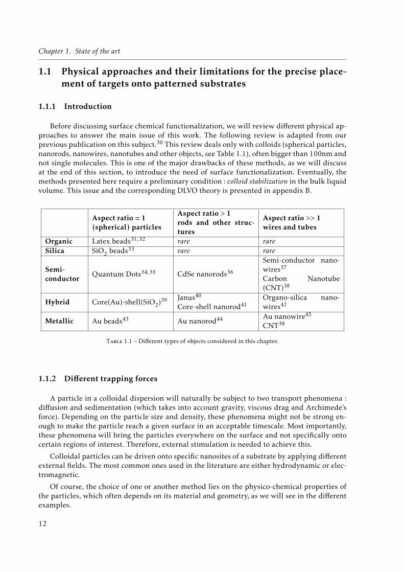
1.1.1 Introduction
Before discussing surface chemical functionalization, we will review different physical ap-proaches to answer the main issue of this work. The following review is adapted from ourprevious publication on this subject.30 This review deals only with colloids (spherical particles,nanorods, nanowires, nanotubes and other objects, see Table 1.1), often bigger than 100nm andnot single molecules. This is one of the major drawbacks of these methods, as we will discussat the end of this section, to introduce the need of surface functionalization. Eventually, themethods presented here require a preliminary condition : colloid stabilization in the bulk liquidvolume. This issue and the corresponding DLVO theory is presented in appendix B.
Aspect ratio = 1(spherical) particles
Aspect ratio > 1rods and other struc-tures
Aspect ratio >> 1wires and tubes
Organic Latex beads31, 32 rare rareSilica SiO2 beads33 rare rare
Semi-conductor
Quantum Dots34, 35 CdSe nanorods36
Semi-conductor nano-wires37
Carbon Nanotube(CNT)38
Hybrid Core(Au)-shell(SiO2)39 Janus40
Core-shell nanorod41Organo-silica nano-wires42
Metallic Au beads43 Au nanorod44 Au nanowire45
CNT38
Table 1.1 – Different types of objects considered in this chapter.
1.1.2 Different trapping forces
A particle in a colloidal dispersion will naturally be subject to two transport phenomena :diffusion and sedimentation (which takes into account gravity, viscous drag and Archimede’sforce). Depending on the particle size and density, these phenomena might not be strong en-ough to make the particle reach a given surface in an acceptable timescale. Most importantly,these phenomena will bring the particles everywhere on the surface and not specifically ontocertain regions of interest. Therefore, external stimulation is needed to achieve this.
Colloidal particles can be driven onto specific nanosites of a substrate by applying differentexternal fields. The most common ones used in the literature are either hydrodynamic or elec-tromagnetic.
Of course, the choice of one or another method lies on the physico-chemical properties ofthe particles, which often depends on its material and geometry, as we will see in the differentexamples.
12
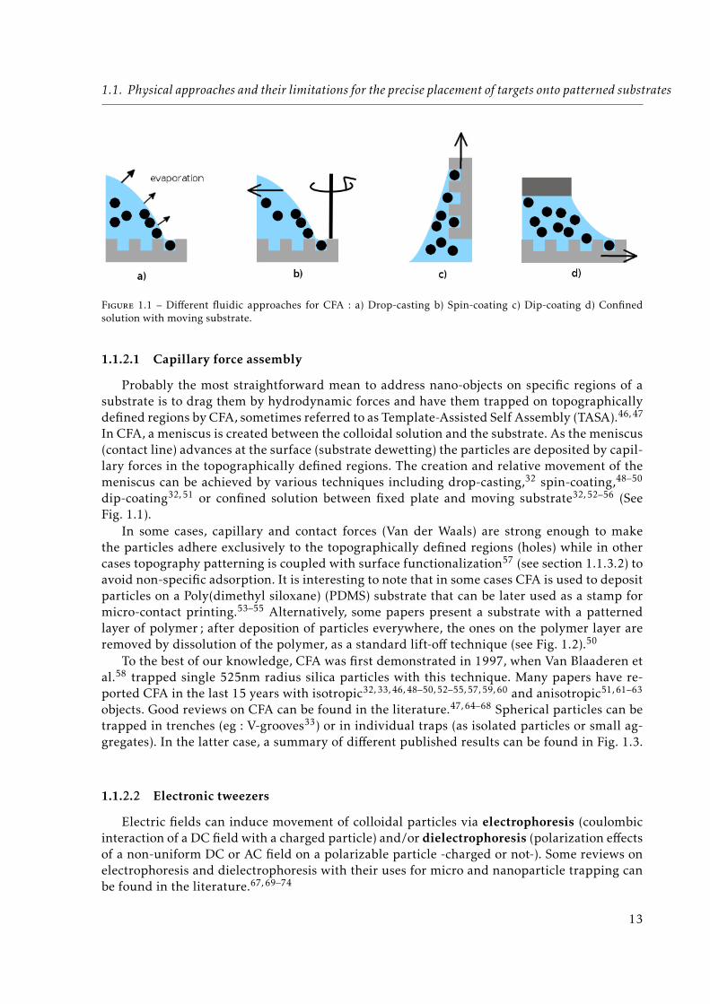
1.1. Physical approaches and their limitations for the precise placement of targets onto patterned substrates
Figure 1.1 – Different fluidic approaches for CFA : a) Drop-casting b) Spin-coating c) Dip-coating d) Confinedsolution with moving substrate.
1.1.2.1 Capillary force assembly
Probably the most straightforward mean to address nano-objects on specific regions of asubstrate is to drag them by hydrodynamic forces and have them trapped on topographicallydefined regions by CFA, sometimes referred to as Template-Assisted Self Assembly (TASA).46, 47
In CFA, a meniscus is created between the colloidal solution and the substrate. As the meniscus(contact line) advances at the surface (substrate dewetting) the particles are deposited by capil-lary forces in the topographically defined regions. The creation and relative movement of themeniscus can be achieved by various techniques including drop-casting,32 spin-coating,48–50
dip-coating32, 51 or confined solution between fixed plate and moving substrate32, 52–56 (SeeFig. 1.1).
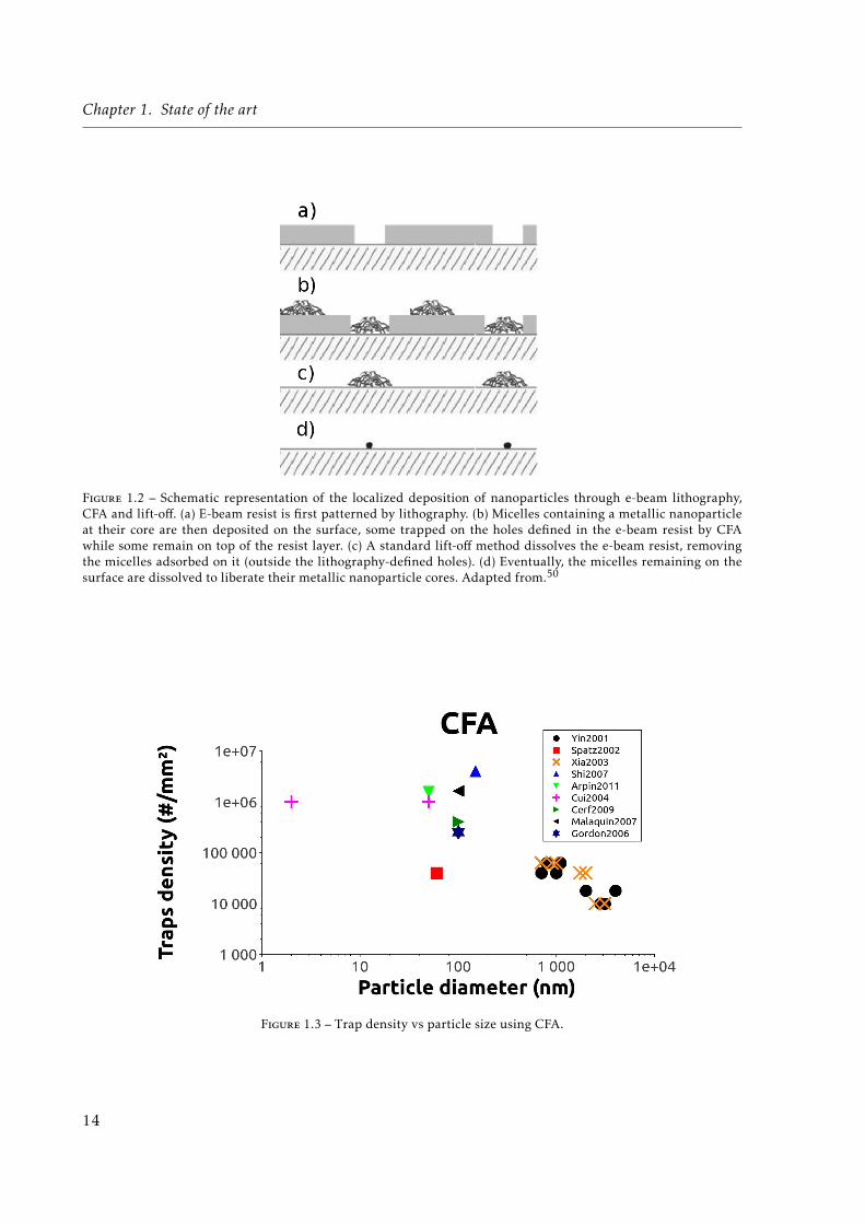
In some cases, capillary and contact forces (Van der Waals) are strong enough to makethe particles adhere exclusively to the topographically defined regions (holes) while in othercases topography patterning is coupled with surface functionalization57 (see section 1.1.3.2) toavoid non-specific adsorption. It is interesting to note that in some cases CFA is used to depositparticles on a Poly(dimethyl siloxane) (PDMS) substrate that can be later used as a stamp formicro-contact printing.53–55 Alternatively, some papers present a substrate with a patternedlayer of polymer ; after deposition of particles everywhere, the ones on the polymer layer areremoved by dissolution of the polymer, as a standard lift-off technique (see Fig. 1.2).50
To the best of our knowledge, CFA was first demonstrated in 1997, when Van Blaaderen etal.58 trapped single 525nm radius silica particles with this technique. Many papers have re-ported CFA in the last 15 years with isotropic32, 33, 46, 48–50, 52–55, 57, 59, 60 and anisotropic51, 61–63
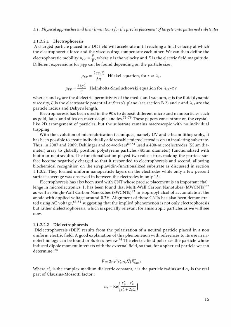
objects. Good reviews on CFA can be found in the literature.47, 64–68 Spherical particles can betrapped in trenches (eg : V-grooves33) or in individual traps (as isolated particles or small ag-gregates). In the latter case, a summary of different published results can be found in Fig. 1.3.
1.1.2.2 Electronic tweezers
Electric fields can induce movement of colloidal particles via electrophoresis (coulombicinteraction of a DC field with a charged particle) and/or dielectrophoresis (polarization effectsof a non-uniform DC or AC field on a polarizable particle -charged or not-). Some reviews onelectrophoresis and dielectrophoresis with their uses for micro and nanoparticle trapping canbe found in the literature.67, 69–74
13
Chapter 1. State of the art
Figure 1.2 – Schematic representation of the localized deposition of nanoparticles through e-beam lithography,CFA and lift-off. (a) E-beam resist is first patterned by lithography. (b) Micelles containing a metallic nanoparticleat their core are then deposited on the surface, some trapped on the holes defined in the e-beam resist by CFAwhile some remain on top of the resist layer. (c) A standard lift-off method dissolves the e-beam resist, removingthe micelles adsorbed on it (outside the lithography-defined holes). (d) Eventually, the micelles remaining on thesurface are dissolved to liberate their metallic nanoparticle cores. Adapted from.50
Figure 1.3 – Trap density vs particle size using CFA.
14
1.1. Physical approaches and their limitations for the precise placement of targets onto patterned substrates
1.1.2.2.1 ElectrophoresisA charged particle placed in a DC field will accelerate until reaching a final velocity at which
the electrophoretic force and the viscous drag compensate each other. We can then define theelectrophoretic mobility µEP =
vE
, where v is the velocity and E is the electric field magnitude.
Different expressions for µEP can be found depending on the particle size :
µEP =2εε0ζ
3ηHückel equation, for r � λD
µEP =εε0ζη
Helmholtz-Smoluchowski equation for λD � r
where ε and ε0 are the dielectric permittivity of the media and vacuum, η is the fluid dynamicviscosity, ζ is the electrostatic potential at Stern’s plane (see section B.2) and r and λD are theparticle radius and Debye’s length.
Electrophoresis has been used in the 90’s to deposit different micro and nanoparticles suchas gold, latex and silica on macroscopic anodes.75–79 These papers concentrate on the crystal-like 2D arrangement of particles, but the substrate remains macroscopic with no individualtrapping.
With the evolution of microfabrication techniques, namely UV and e-beam lithography, ithas been possible to create individually addressable microelectrodes on an insulating substrate.Thus, in 2007 and 2009, Dehlinger and co-workers80, 81 used a 400-microelectrodes (55µm dia-meter) array to globally position polystyrene particles (40nm diameter) functionalized withbiotin or neutravidin. The functionalization played two roles : first, making the particle sur-face become negatively charged so that it responded to electrophoresis and second, allowingbiochemical recognition on the streptavidin-functionalized substrate as discussed in section1.1.3.2. They formed uniform nanoparticle layers on the electrodes while only a few percentsurface coverage was observed in between the electrodes in only 15s.
Electrophoresis has also been used with CNT whose precise placement is an important chal-lenge in microelectronics. It has been found that Multi-Wall Carbon Nanotubes (MWCNTs)82
as well as Single-Wall Carbon Nanotubes (SWCNTs)83 in isopropyl alcohol accumulate at theanode with applied voltage around 0.7V. Alignment of these CNTs has also been demonstra-ted using AC voltage,83, 84 suggesting that the implied phenomenon is not only electrophoresisbut rather dielectrophoresis, which is specially relevant for anisotropic particles as we will seenow.
1.1.2.2.2 DielectrophoresisDielectrophoresis (DEP) results from the polarization of a neutral particle placed in a non
uniform electric field. A good explanation of this phenomenon with references to its use in na-notechnology can be found in Burke’s review.74 The electric field polarizes the particle whoseinduced dipole moment interacts with the external field, so that, for a spherical particle we candetermine :85
~F = 2πr3ε∗mαr~∇(~E2rms)
Where ε∗m is the complex medium dielectric constant, r is the particle radius and αr is the realpart of Clausius-Mossotti factor :
αr = Re(ε∗p − ε∗mε∗p + 2ε∗m
)15

Chapter 1. State of the art
Where ε∗p is the particle dielectric constant.From the expression of αr we can see that it can be either positive, inducing particles to movetoward maximum electric field region (positive dielectrophoresis) or negative, inducing particlesto move toward minimum electric field region (negative dielectrophoresis). Moreover because of
dispersion we have ε∗ = ε∗(σ,ω) = ε − j σω
, (σ being the conductivity and ω the field frequency)
which means that the same particle in the same medium may experience positive or negativedielectrophoresis depending on σ and ω86 (the frequency for which αr(ω) = 0 is called thecrossover frequency). For a further study on this subject and on the role of the electric doublelayer, one may read Hughes’ article from 2002.87
The first description and preliminary results of dielectrophoresis were given by HerbertAckland Pohl in the 50’s88, 89 with a more comprehensive study in 1978.90 Since then, andspecially with improved lithography techniques for microelectrode design, dielectrophoresishas been widely used for particle trapping. Since the late 90’s, most reported results in theliterature have been obtained with latex beads. The reasons for this relate to the fact that theyare commercially available in different sizes and can be fluorescently labeled.74
Many experimental results were presented mainly by Fuhr’s and Morgan and Hughes’groups. In these papers31, 85, 86, 91–103 nanoparticles ranking from 14nm93 to 93nm96 have beentrapped using different electrode geometries and voltages. From the beginning of the years2000’s until today, DEP has been used with organic latexes in a certain number of papers80, 81, 104–129
but these contributions mainly focus on the application of DEP to biological samples (cells, vi-ruses, biomolecules...) and on ever more complex systems.
Dielectrophoretic trapping of metallic and semiconductor nanoparticles has also been re-ported and remains a field of active research. In 1997, Bezryadin and Dekker130, 131 demons-trated the possibility of bridging Pt nanoelectrodes with gaps as small as 4nm with Pd colloids(as small as 17nm) trapped individually. Further work has been conducted with 60nm and40nm gold nanoparticles (Clausius-Mossotti factor can be assumed to be equal to +1 in mostcases)132 by Krahne et al.133, 134 to fill a 10nm gap. Similar results were found independentlyby Amlani, Rawlett et al.135–137 Other groups used 20nm beads to bridge gaps of different sizesranging from 5 to 150nm.43, 138, 139 These papers also demonstrate the gap-size-dependency ofthe previously noticed134 threshold voltage.138 Two interesting approaches were described byKhondaker and Yao140 who used 50nm gold colloids to bridge a large gap (400nm bridged bya collection of particles and 45nm bridged by a single particle) and subsequently broke thatbridge by applying a strong DC voltage, thus resulting in sub-10nm gaps. Zheng et al.104 usedcarbon nanotubes as the electrodes for DEP trapping of gold colloids as small as 2nm, albeitnot as single particle trapping. Finally, gold colloids have also been trapped as dimers, linkedby dithiol.141, 142
We have seen how spherical particles can be trapped by DEP. Nonetheless it is obvious thatparticles having a geometrical anisotropy (nanorods, nanowires and nanotubes) are perfectcandidates for dielectrophoretic trapping as the polarization can occur preferentially along thelong axis. Moreover, DEP trapping is often used for the purpose of bridging two electrodes.Thus, one needs a particle with one dimension larger than the others in combination withmetallic or semiconducting properties.
For all these reasons, extensive literature can be found on DEP using nanowires that canbe either metallic (such as Au,44, 45, 143–145 Ag,146 NiSi147 and Rh148, 149), semiconducting withdifferent energy gaps (Si,144, 149–151 ZnO,152–158 SnO2,146, 159 GaN,146, 160–166 InAs,167 SiC168
and Ga2O3146 among others) or more complex materials.169 In the past 5 years, different pa-
16
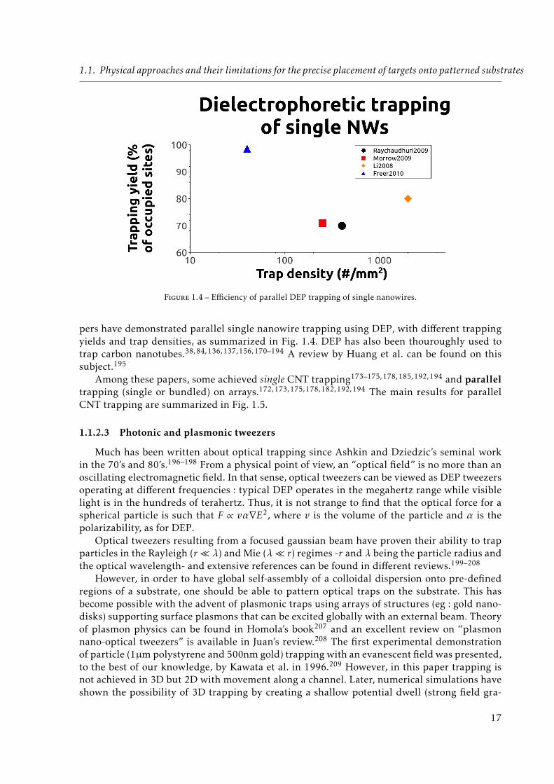
1.1. Physical approaches and their limitations for the precise placement of targets onto patterned substrates
Figure 1.4 – Efficiency of parallel DEP trapping of single nanowires.
pers have demonstrated parallel single nanowire trapping using DEP, with different trappingyields and trap densities, as summarized in Fig. 1.4. DEP has also been thouroughly used totrap carbon nanotubes.38, 84, 136, 137, 156, 170–194 A review by Huang et al. can be found on thissubject.195
Among these papers, some achieved single CNT trapping173–175, 178, 185, 192, 194 and paralleltrapping (single or bundled) on arrays.172, 173, 175, 178, 182, 192, 194 The main results for parallelCNT trapping are summarized in Fig. 1.5.
1.1.2.3 Photonic and plasmonic tweezers
Much has been written about optical trapping since Ashkin and Dziedzic’s seminal workin the 70’s and 80’s.196–198 From a physical point of view, an “optical field” is no more than anoscillating electromagnetic field. In that sense, optical tweezers can be viewed as DEP tweezersoperating at different frequencies : typical DEP operates in the megahertz range while visiblelight is in the hundreds of terahertz. Thus, it is not strange to find that the optical force for aspherical particle is such that F ∝ vα∇E2, where v is the volume of the particle and α is thepolarizability, as for DEP.
Optical tweezers resulting from a focused gaussian beam have proven their ability to trapparticles in the Rayleigh (r � λ) and Mie (λ� r) regimes -r and λ being the particle radius andthe optical wavelength- and extensive references can be found in different reviews.199–208
However, in order to have global self-assembly of a colloidal dispersion onto pre-definedregions of a substrate, one should be able to pattern optical traps on the substrate. This hasbecome possible with the advent of plasmonic traps using arrays of structures (eg : gold nano-disks) supporting surface plasmons that can be excited globally with an external beam. Theoryof plasmon physics can be found in Homola’s book207 and an excellent review on “plasmonnano-optical tweezers” is available in Juan’s review.208 The first experimental demonstrationof particle (1µm polystyrene and 500nm gold) trapping with an evanescent field was presented,to the best of our knowledge, by Kawata et al. in 1996.209 However, in this paper trapping isnot achieved in 3D but 2D with movement along a channel. Later, numerical simulations haveshown the possibility of 3D trapping by creating a shallow potential dwell (strong field gra-
17
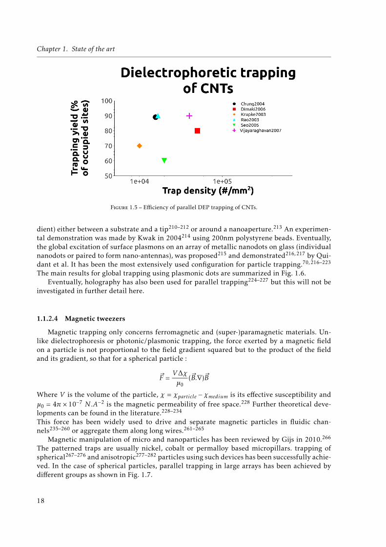
Chapter 1. State of the art
Figure 1.5 – Efficiency of parallel DEP trapping of CNTs.
dient) either between a substrate and a tip210–212 or around a nanoaperture.213 An experimen-tal demonstration was made by Kwak in 2004214 using 200nm polystyrene beads. Eventually,the global excitation of surface plasmons on an array of metallic nanodots on glass (individualnanodots or paired to form nano-antennas), was proposed215 and demonstrated216, 217 by Qui-dant et al. It has been the most extensively used configuration for particle trapping.70, 216–223
The main results for global trapping using plasmonic dots are summarized in Fig. 1.6.Eventually, holography has also been used for parallel trapping224–227 but this will not be
investigated in further detail here.
1.1.2.4 Magnetic tweezers
Magnetic trapping only concerns ferromagnetic and (super-)paramagnetic materials. Un-like dielectrophoresis or photonic/plasmonic trapping, the force exerted by a magnetic fieldon a particle is not proportional to the field gradient squared but to the product of the fieldand its gradient, so that for a spherical particle :
~F =V∆χµ0
(~B.∇)~B
Where V is the volume of the particle, χ = χparticle −χmedium is its effective susceptibility andµ0 = 4π × 10−7 N.A−2 is the magnetic permeability of free space.228 Further theoretical deve-lopments can be found in the literature.228–234
This force has been widely used to drive and separate magnetic particles in fluidic chan-nels235–260 or aggregate them along long wires.261–265
Magnetic manipulation of micro and nanoparticles has been reviewed by Gijs in 2010.266
The patterned traps are usually nickel, cobalt or permalloy based micropillars. trapping ofspherical267–276 and anisotropic277–282 particles using such devices has been successfully achie-ved. In the case of spherical particles, parallel trapping in large arrays has been achieved bydifferent groups as shown in Fig. 1.7.
18
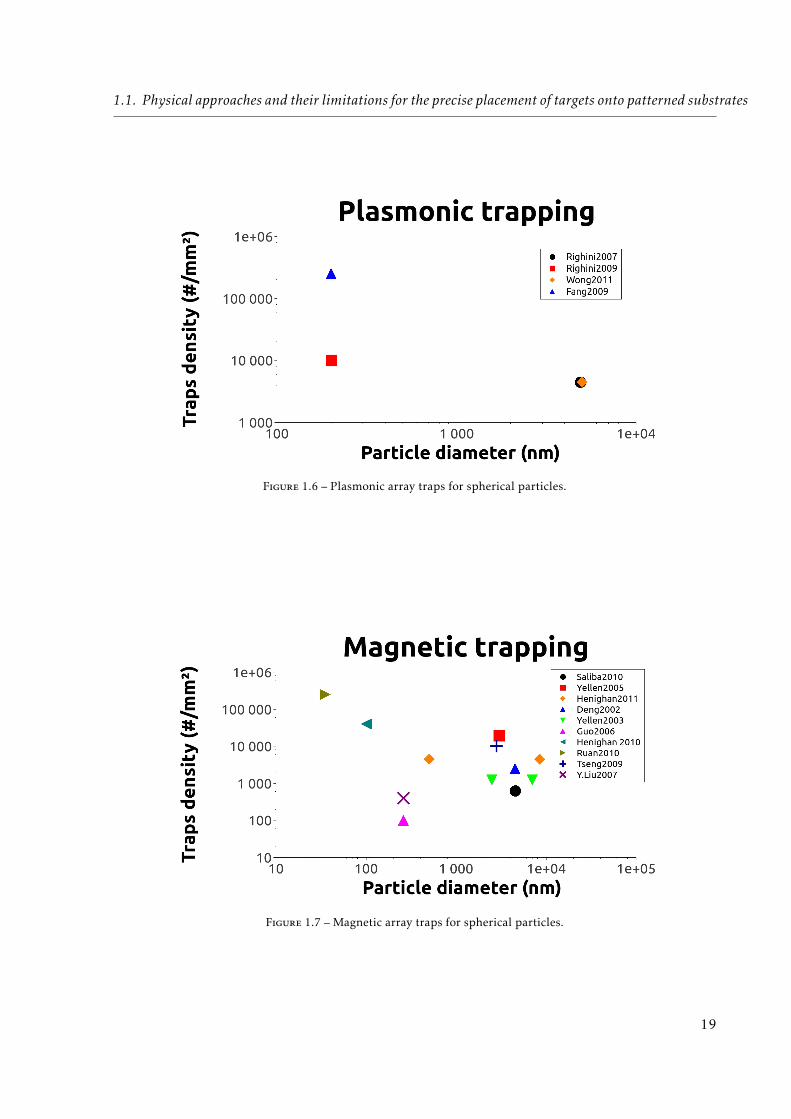
1.1. Physical approaches and their limitations for the precise placement of targets onto patterned substrates
Figure 1.6 – Plasmonic array traps for spherical particles.
Figure 1.7 – Magnetic array traps for spherical particles.
19
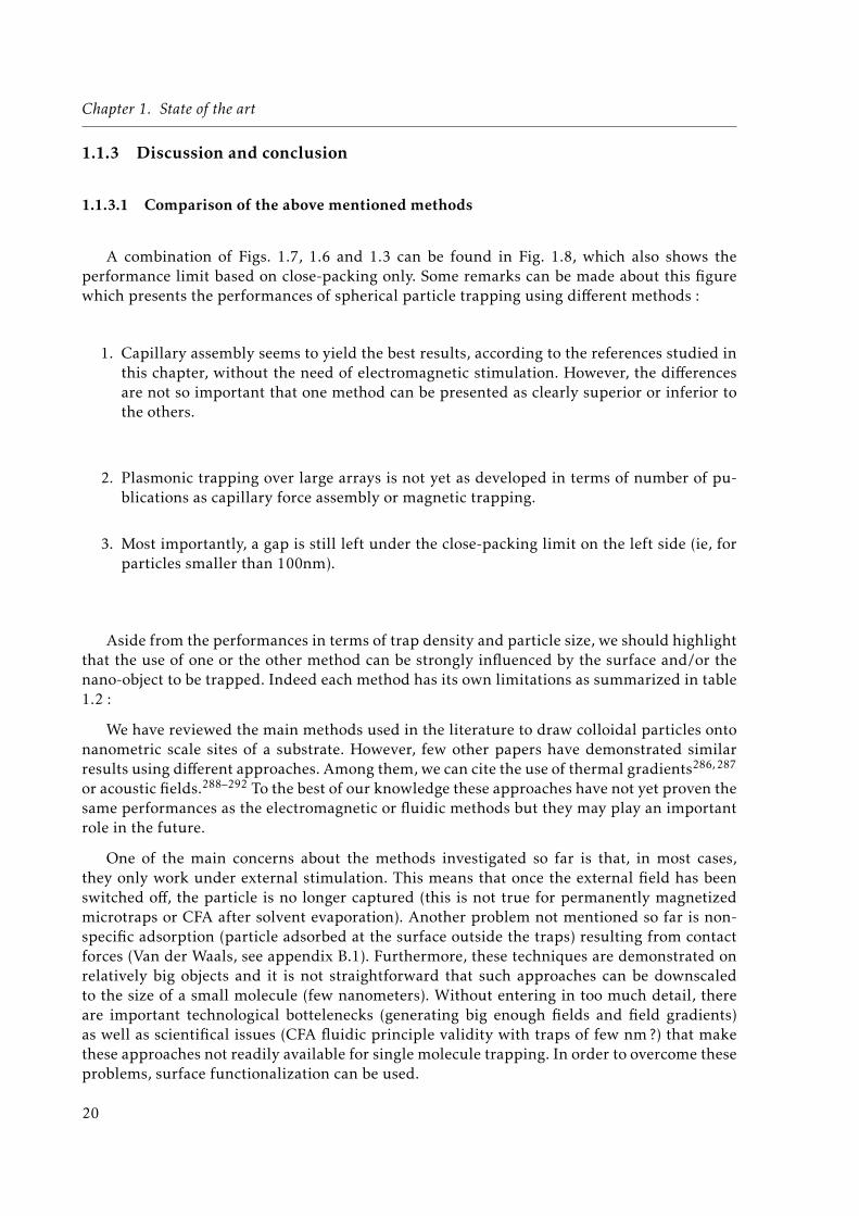
Chapter 1. State of the art
1.1.3 Discussion and conclusion
1.1.3.1 Comparison of the above mentioned methods
A combination of Figs. 1.7, 1.6 and 1.3 can be found in Fig. 1.8, which also shows theperformance limit based on close-packing only. Some remarks can be made about this figurewhich presents the performances of spherical particle trapping using different methods :
1. Capillary assembly seems to yield the best results, according to the references studied inthis chapter, without the need of electromagnetic stimulation. However, the differencesare not so important that one method can be presented as clearly superior or inferior tothe others.
2. Plasmonic trapping over large arrays is not yet as developed in terms of number of pu-blications as capillary force assembly or magnetic trapping.
3. Most importantly, a gap is still left under the close-packing limit on the left side (ie, forparticles smaller than 100nm).
Aside from the performances in terms of trap density and particle size, we should highlightthat the use of one or the other method can be strongly influenced by the surface and/or thenano-object to be trapped. Indeed each method has its own limitations as summarized in table1.2 :
We have reviewed the main methods used in the literature to draw colloidal particles ontonanometric scale sites of a substrate. However, few other papers have demonstrated similarresults using different approaches. Among them, we can cite the use of thermal gradients286, 287
or acoustic fields.288–292 To the best of our knowledge these approaches have not yet proven thesame performances as the electromagnetic or fluidic methods but they may play an importantrole in the future.
One of the main concerns about the methods investigated so far is that, in most cases,they only work under external stimulation. This means that once the external field has beenswitched off, the particle is no longer captured (this is not true for permanently magnetizedmicrotraps or CFA after solvent evaporation). Another problem not mentioned so far is non-specific adsorption (particle adsorbed at the surface outside the traps) resulting from contactforces (Van der Waals, see appendix B.1). Furthermore, these techniques are demonstrated onrelatively big objects and it is not straightforward that such approaches can be downscaledto the size of a small molecule (few nanometers). Without entering in too much detail, thereare important technological bottelenecks (generating big enough fields and field gradients)as well as scientifical issues (CFA fluidic principle validity with traps of few nm ?) that makethese approaches not readily available for single molecule trapping. In order to overcome theseproblems, surface functionalization can be used.
20
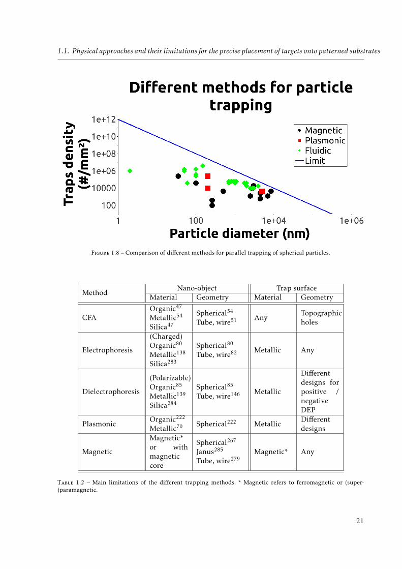
1.1. Physical approaches and their limitations for the precise placement of targets onto patterned substrates
Figure 1.8 – Comparison of different methods for parallel trapping of spherical particles.
MethodNano-object Trap surface
Material Geometry Material Geometry
CFAOrganic47
Metallic54
Silica47
Spherical54
Tube, wire51 AnyTopographicholes
Electrophoresis
(Charged)Organic80
Metallic138
Silica283
Spherical80
Tube, wire82 Metallic Any
Dielectrophoresis
(Polarizable)Organic85
Metallic139
Silica284
Spherical85
Tube, wire146 Metallic
Differentdesigns forpositive /negativeDEP
PlasmonicOrganic222
Metallic70 Spherical222 MetallicDifferentdesigns
Magnetic
Magnetic*or withmagneticcore
Spherical267
Janus285
Tube, wire279Magnetic* Any
Table 1.2 – Main limitations of the different trapping methods. * Magnetic refers to ferromagnetic or (super-)paramagnetic.
21
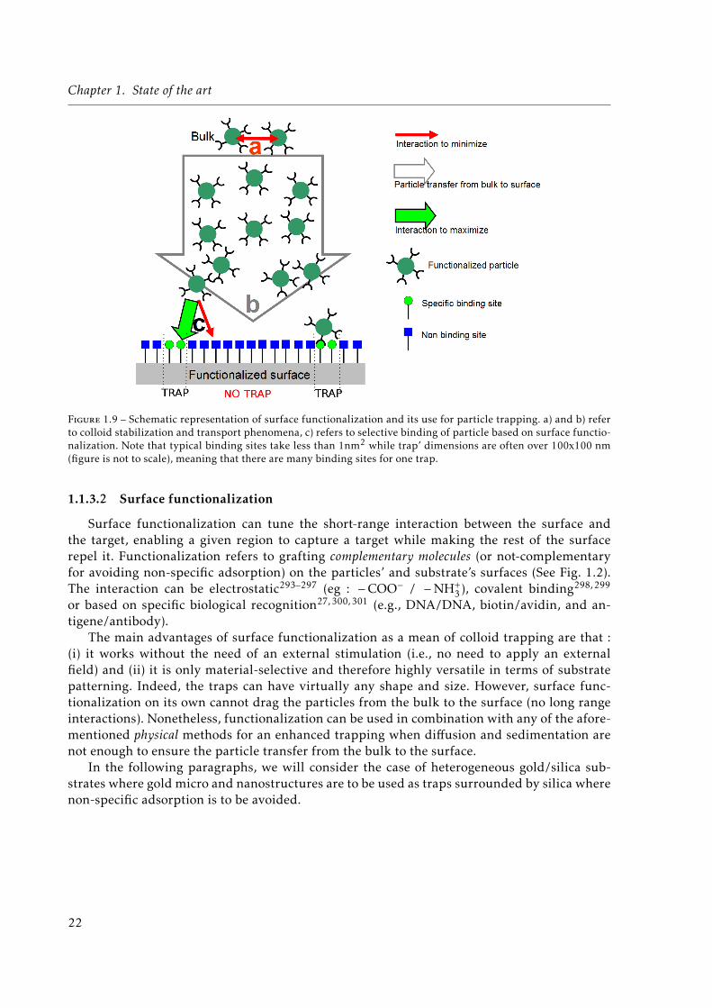
Chapter 1. State of the art
Figure 1.9 – Schematic representation of surface functionalization and its use for particle trapping. a) and b) referto colloid stabilization and transport phenomena, c) refers to selective binding of particle based on surface functio-nalization. Note that typical binding sites take less than 1nm2 while trap’ dimensions are often over 100x100 nm(figure is not to scale), meaning that there are many binding sites for one trap.
1.1.3.2 Surface functionalization
Surface functionalization can tune the short-range interaction between the surface andthe target, enabling a given region to capture a target while making the rest of the surfacerepel it. Functionalization refers to grafting complementary molecules (or not-complementaryfor avoiding non-specific adsorption) on the particles’ and substrate’s surfaces (See Fig. 1.2).The interaction can be electrostatic293–297 (eg : −COO− / −NH+
3 ), covalent binding298, 299
or based on specific biological recognition27, 300, 301 (e.g., DNA/DNA, biotin/avidin, and an-tigene/antibody).
The main advantages of surface functionalization as a mean of colloid trapping are that :(i) it works without the need of an external stimulation (i.e., no need to apply an externalfield) and (ii) it is only material-selective and therefore highly versatile in terms of substratepatterning. Indeed, the traps can have virtually any shape and size. However, surface func-tionalization on its own cannot drag the particles from the bulk to the surface (no long rangeinteractions). Nonetheless, functionalization can be used in combination with any of the afore-mentioned physical methods for an enhanced trapping when diffusion and sedimentation arenot enough to ensure the particle transfer from the bulk to the surface.
In the following paragraphs, we will consider the case of heterogeneous gold/silica sub-strates where gold micro and nanostructures are to be used as traps surrounded by silica wherenon-specific adsorption is to be avoided.
22
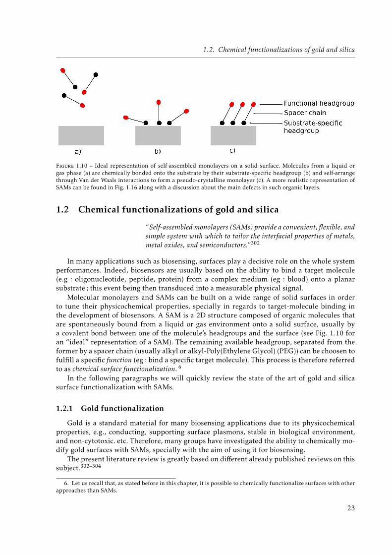
1.2. Chemical functionalizations of gold and silica
Figure 1.10 – Ideal representation of self-assembled monolayers on a solid surface. Molecules from a liquid orgas phase (a) are chemically bonded onto the substrate by their substrate-specific headgroup (b) and self-arrangethrough Van der Waals interactions to form a pseudo-crystalline monolayer (c). A more realistic representation ofSAMs can be found in Fig. 1.16 along with a discussion about the main defects in such organic layers.
1.2 Chemical functionalizations of gold and silica
“Self-assembled monolayers (SAMs) provide a convenient, flexible, andsimple system with which to tailor the interfacial properties of metals,metal oxides, and semiconductors.”302
In many applications such as biosensing, surfaces play a decisive role on the whole systemperformances. Indeed, biosensors are usually based on the ability to bind a target molecule(e.g : oligonucleotide, peptide, protein) from a complex medium (eg : blood) onto a planarsubstrate ; this event being then transduced into a measurable physical signal.
Molecular monolayers and SAMs can be built on a wide range of solid surfaces in orderto tune their physicochemical properties, specially in regards to target-molecule binding inthe development of biosensors. A SAM is a 2D structure composed of organic molecules thatare spontaneously bound from a liquid or gas environment onto a solid surface, usually bya covalent bond between one of the molecule’s headgroups and the surface (see Fig. 1.10 foran “ideal” representation of a SAM). The remaining available headgroup, separated from theformer by a spacer chain (usually alkyl or alkyl-Poly(Ethylene Glycol) (PEG)) can be choosen tofulfill a specific function (eg : bind a specific target molecule). This process is therefore referredto as chemical surface functionalization. 6
In the following paragraphs we will quickly review the state of the art of gold and silicasurface functionalization with SAMs.
1.2.1 Gold functionalization
Gold is a standard material for many biosensing applications due to its physicochemicalproperties, e.g., conducting, supporting surface plasmons, stable in biological environment,and non-cytotoxic. etc. Therefore, many groups have investigated the ability to chemically mo-dify gold surfaces with SAMs, specially with the aim of using it for biosensing.
The present literature review is greatly based on different already published reviews on thissubject.302–304
6. Let us recall that, as stated before in this chapter, it is possible to chemically functionalize surfaces with otherapproaches than SAMs.
23

Chapter 1. State of the art
1.2.1.1 Different molecules
As we have seen in Figure 1.10, the molecules that form a SAM have three main elements :
1. A substrate-binding headgroup
2. A spacer chain
3. A functional headgroup
Let us investigate now the reported possibilities for each of the aforementioned elements in thecase of gold surface functionalization.
1.2.1.1.1 Gold-binding headgroupSome of the chemical groups reported in the literature to bind an organic molecule onto a goldsurface can be found in Table 1.3. 7
7. It should be noted that the molecule’s name is often used for the defining headgroup. Thus, although a thiol isan organic compound with a sulfhydryl headgroup (as an alcohol presents an hydroxyl headgroup), the sulfhydrylgroup itself is often referred to, and will also be in this manuscript, as thiol.
24
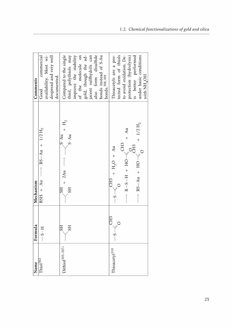
1.2. Chemical functionalizations of gold and silicaN
ame
Form
ula
Mec
han
ism
Com
men
tsT
hiol
302
SH
RSH
+A
uR
S−A
u+
1/2
H2
Goo
dco
mm
erci
alav
aila
bili
ty.
Mos
tw
i-d
esp
read
and
very
wel
ld
ocu
men
ted
.
Dit
hiol
305–
307∗
SHSH
SHSH+
2Au
SA
u
SA
u+
H2
Com
par
edto
the
sing
leth
iol,
pol
ythi
ols
may
imp
rove
the
stab
ilit
yof
the
mol
ecu
leon
gold
,th
ough
the
ad-
jace
ntsu
lfhy
dri
lsca
nal
sofo
rmd
isu
lfid
ebo
nds
inst
ead
ofS-
Au
bond
s.30
8,30
9
Thi
oace
tyl31
0S
OCH
3S
OCH
3+
H2O
+A
u
R−S−H
+H
OOC
H3
+A
u
RS−A
u+
HO
OCH
3+
1/2
H2
Thi
oace
tyls
are
ap
ro-
tect
edfo
rmof
thio
lsto
avoi
dox
idat
ion.
De-
pro
tect
ion
(hyd
roly
sis)
isbe
tter
per
form
edu
nder
basi
cco
ndit
ions
wit
hN
H4O
H
25

Chapter 1. State of the artN
ame
Form
ula
Mec
han
ism
Com
men
tsSu
lfid
e311
SR′
R−S−R′
+A
uR
SA
uR′
Itis
beli
eved
that
dia
l-ky
lsu
lfid
esbo
ndon
togo
ldth
rou
gha
dat
ive
bond
,wit
hou
tcl
eava
geof
the
C-S
bond
sof
the
sulfi
de.
Thi
sac
-co
unt
sfo
rth
ew
eake
rro
bust
ness
com
par
edto
SAM
sfo
rmed
from
thio
lsor
dis
ulfi
des
.H
owev
er,
assy
met
ric
sulfi
des
are
inte
rest
ing
tost
ud
ym
ixed
-SA
Ms
cont
aini
ngd
iffer
ent
chai
nsor
head
grou
ps
whi
char
ene
cess
aril
yw
ell-
mix
ed(b
ecau
seco
vale
ntly
bond
ed).30
2
Dis
ulfi
de31
2S
SR′
R−S−S−R′
+2A
uR−S−A
u+
R′ −
S−A
uD
isu
lfid
esca
nfo
rmas
thio
lsge
tox
idiz
edw
hen
stor
edin
air
cond
itio
n,le
adin
gth
us
toa
low
erso
lubi
lity
than
not-
oxid
ized
thio
ls.30
2A
ssym
etri
cd
isu
lfid
es(d
iffer
ent
Ran
dR
’gr
oup
s)le
adto
mix
ed-S
AM
s.
26
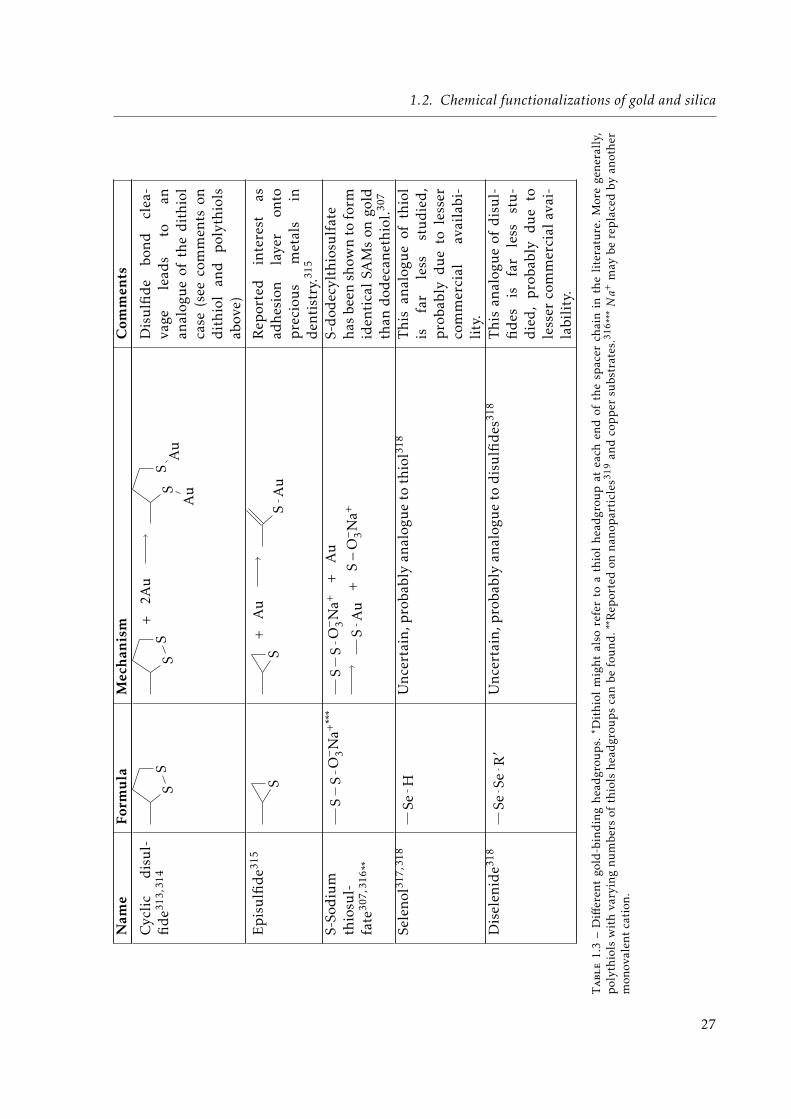
1.2. Chemical functionalizations of gold and silicaN
ame
Form
ula
Mec
han
ism
Com
men
ts
Cyc
lic
dis
ul-
fid
e313,
314
SS
SS
+2A
u
SA
u
SA
u
Dis
ulfi
de
bond
clea
-va
gele
ads
toan
anal
ogu
eof
the
dit
hiol
case
(see
com
men
tson
dit
hiol
and
pol
ythi
ols
abov
e)
Ep
isu
lfid
e315
SS
+A
uS
Au
Rep
orte
din
tere
stas
adhe
sion
laye
ron
top
reci
ous
met
als
ind
enti
stry
.315
S-So
diu
mth
iosu
l-fa
te30
7,31
6∗∗
SS
O− 3N
a+∗∗∗
SS
O− 3N
a++
Au
SA
u+
S−O
− 3N
a+S-
dod
ecyl
thio
sulf
ate
has
been
show
nto
form
iden
tica
lSA
Ms
ongo
ldth
and
odec
anet
hiol
.307
Sele
nol31
7,31
8Se
HU
ncer
tain
,pro
babl
yan
alog
ue
toth
iol31
8T
his
anal
ogu
eof
thio
lis
far
less
stu
die
d,
pro
babl
ydu
eto
less
erco
mm
erci
alav
aila
bi-
lity
.D
isel
enid
e318
SeSe
R′
Unc
erta
in,p
roba
bly
anal
ogu
eto
dis
ulfi
des
318
Thi
san
alog
ue
ofd
isu
l-fi
des
isfa
rle
ssst
u-
die
d,
pro
babl
ydu
eto
less
erco
mm
erci
alav
ai-
labi
lity
.
Table
1.3
–D
iffer
ent
gold
-bin
din
ghe
adgr
oup
s.∗ D
ithi
olm
ight
also
refe
rto
ath
iol
head
grou
pat
each
end
ofth
esp
acer
chai
nin
the
lite
ratu
re.
Mor
ege
nera
lly,
pol
ythi
ols
wit
hva
ryin
gnu
mbe
rsof
thio
lshe
adgr
oup
sca
nbe
fou
nd.∗∗ R
epor
ted
onna
nop
arti
cles
319
and
cop
per
subs
trat
es.31
6∗∗∗Na+
may
bere
pla
ced
byan
othe
rm
onov
alen
tca
tion
.
27
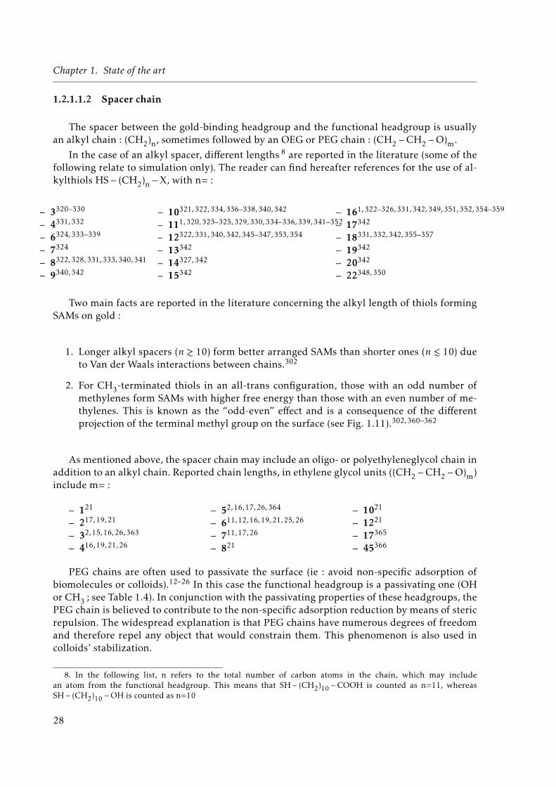
Chapter 1. State of the art
1.2.1.1.2 Spacer chain
The spacer between the gold-binding headgroup and the functional headgroup is usuallyan alkyl chain : (CH2)n, sometimes followed by an OEG or PEG chain : (CH2 −CH2 −O)m.
In the case of an alkyl spacer, different lengths 8 are reported in the literature (some of thefollowing relate to simulation only). The reader can find hereafter references for the use of al-kylthiols HS− (CH2)n −X, with n= :
– 3320–330
– 4331, 332
– 6324, 333–339
– 7324
– 8322, 328, 331, 333, 340, 341
– 9340, 342
– 10321, 322, 334, 336–338, 340, 342
– 111, 320, 323–325, 329, 330, 334–336, 339, 341–352
– 12322, 331, 340, 342, 345–347, 353, 354
– 13342
– 14327, 342
– 15342
– 161, 322–326, 331, 342, 349, 351, 352, 354–359
– 17342
– 18331, 332, 342, 355–357
– 19342
– 20342
– 22348, 350
Two main facts are reported in the literature concerning the alkyl length of thiols formingSAMs on gold :
1. Longer alkyl spacers (n & 10) form better arranged SAMs than shorter ones (n . 10) dueto Van der Waals interactions between chains.302
2. For CH3-terminated thiols in an all-trans configuration, those with an odd number ofmethylenes form SAMs with higher free energy than those with an even number of me-thylenes. This is known as the “odd-even” effect and is a consequence of the differentprojection of the terminal methyl group on the surface (see Fig. 1.11).302, 360–362
As mentioned above, the spacer chain may include an oligo- or polyethyleneglycol chain inaddition to an alkyl chain. Reported chain lengths, in ethylene glycol units ((CH2 −CH2 −O)m)include m= :
– 121
– 217, 19, 21
– 32, 15, 16, 26, 363
– 416, 19, 21, 26
– 52, 16, 17, 26, 364
– 611, 12, 16, 19, 21, 25, 26
– 711, 17, 26
– 821
– 1021
– 1221
– 17365
– 45366
PEG chains are often used to passivate the surface (ie : avoid non-specific adsorption ofbiomolecules or colloids).12–26 In this case the functional headgroup is a passivating one (OHor CH3 ; see Table 1.4). In conjunction with the passivating properties of these headgroups, thePEG chain is believed to contribute to the non-specific adsorption reduction by means of stericrepulsion. The widespread explanation is that PEG chains have numerous degrees of freedomand therefore repel any object that would constrain them. This phenomenon is also used incolloids’ stabilization.
8. In the following list, n refers to the total number of carbon atoms in the chain, which may includean atom from the functional headgroup. This means that SH− (CH2)10 −COOH is counted as n=11, whereasSH− (CH2)10 −OH is counted as n=10
28
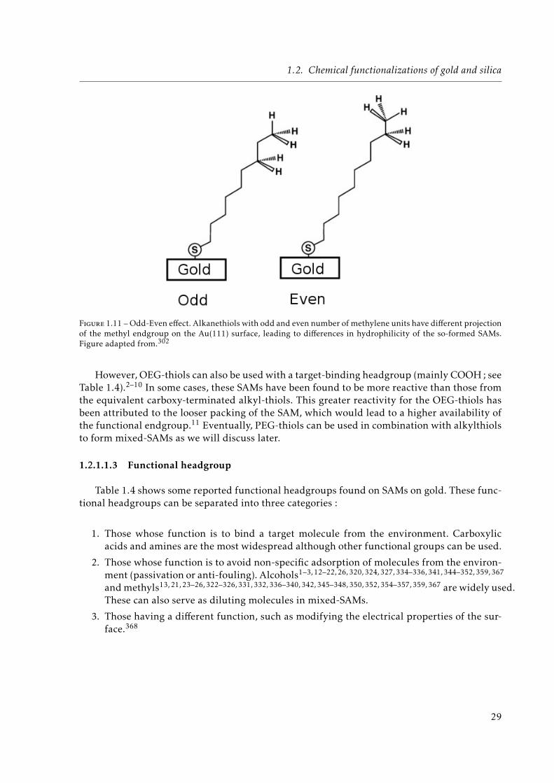
1.2. Chemical functionalizations of gold and silica
Figure 1.11 – Odd-Even effect. Alkanethiols with odd and even number of methylene units have different projectionof the methyl endgroup on the Au(111) surface, leading to differences in hydrophilicity of the so-formed SAMs.Figure adapted from.302
However, OEG-thiols can also be used with a target-binding headgroup (mainly COOH ; seeTable 1.4).2–10 In some cases, these SAMs have been found to be more reactive than those fromthe equivalent carboxy-terminated alkyl-thiols. This greater reactivity for the OEG-thiols hasbeen attributed to the looser packing of the SAM, which would lead to a higher availability ofthe functional endgroup.11 Eventually, PEG-thiols can be used in combination with alkylthiolsto form mixed-SAMs as we will discuss later.
1.2.1.1.3 Functional headgroup
Table 1.4 shows some reported functional headgroups found on SAMs on gold. These func-tional headgroups can be separated into three categories :
1. Those whose function is to bind a target molecule from the environment. Carboxylicacids and amines are the most widespread although other functional groups can be used.
2. Those whose function is to avoid non-specific adsorption of molecules from the environ-ment (passivation or anti-fouling). Alcohols1–3, 12–22, 26, 320, 324, 327, 334–336, 341, 344–352, 359, 367
and methyls13, 21, 23–26, 322–326, 331, 332, 336–340, 342, 345–348, 350, 352, 354–357, 359, 367 are widely used.These can also serve as diluting molecules in mixed-SAMs.
3. Those having a different function, such as modifying the electrical properties of the sur-face.368
29
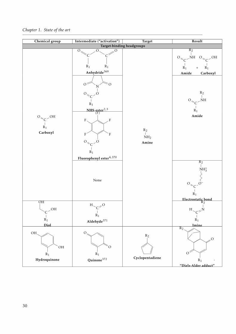
Chapter 1. State of the art
Chemical group Intermediate (“activation”) Target ResultTarget-binding headgroups
R1
CO OH
Carboxyl
R1
CO O
C
O
R1
Anhydride369
R2
NH2
Amine
R1
CO NH
R2
Amide
+ R1
CO OH
Carboxyl
R1
CO O
N OO
NHS-ester2, 3 R1
CO NH
R2
Amide
R1
CO O
F
F
(F)
F
F
Fluorophenyl ester4, 370
None
R1
CO O−
NH+3
R2
Electrostatic bond
R1
COH
OH
Diol
R1
COH
Aldehyde371 R1
CN
R2
H
Imine
R1
OH
HO
Hydroquinone
R1
O
O
Quinone372
R2
CyclopentadieneR1
O
R2
O
-
“Diels-Alder adduct”
30
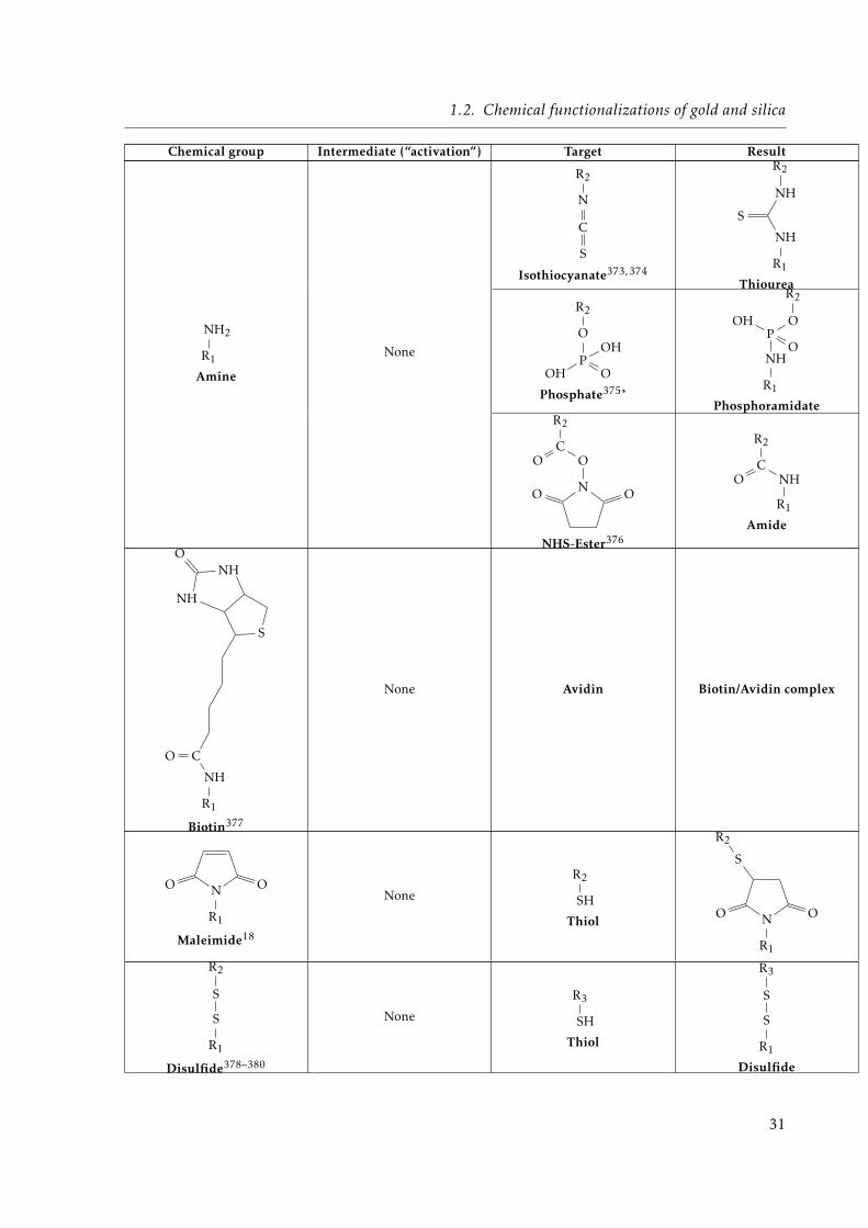
1.2. Chemical functionalizations of gold and silica
Chemical group Intermediate (“activation”) Target Result
R1
NH2
Amine
None
R2
N
C
S
Isothiocyanate373, 374R1
NH
S
NH
R2
Thiourea
R2
O
POH
HO O
Phosphate375∗ R1
NH
PO
HO O
R2
PhosphoramidateR2
CO O
N OO
NHS-Ester376
R2
CO NH
R1
Amide
R1
NH
CO
S
HNO
HN
Biotin377
None Avidin Biotin/Avidin complex
R1
N OO
Maleimide18
None
R2
SH
Thiol
R1
N O
S
R2
O
R1
S
S
R2
Disulfide378–380
None
R3
SH
Thiol R1
S
S
R3
Disulfide
31
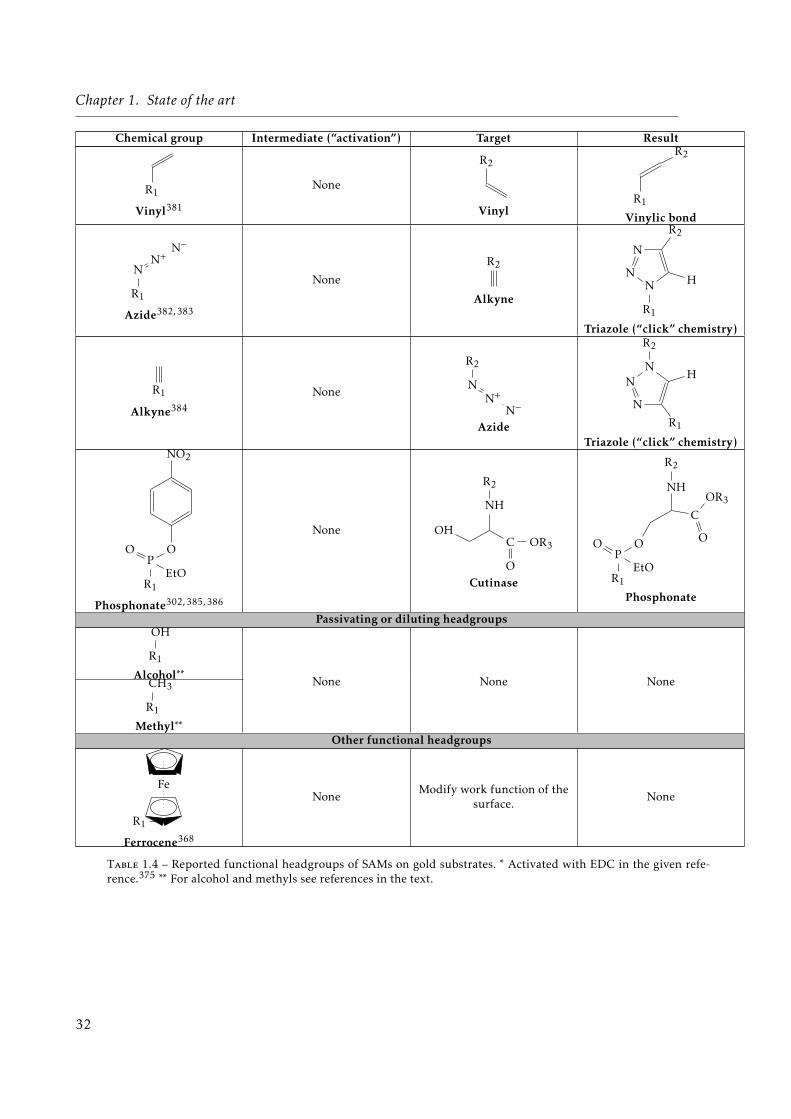
Chapter 1. State of the art
Chemical group Intermediate (“activation”) Target Result
R1
Vinyl381
None
R2
VinylR1
R2
Vinylic bond
R1
NN+
N−
Azide382, 383
None
R2
AlkyneR1
N H
R2
N
N
Triazole (“click” chemistry)
R1
Alkyne384
None
R2
NN+
N−Azide
R2
NH
R1
N
N
Triazole (“click” chemistry)
R1
PEtO
O O
NO2
Phosphonate302, 385, 386
None
R2
NH
HOC
O
OR3
Cutinase R1
PEtO
O O
NH
R2
C
O
OR3
Phosphonate
Passivating or diluting headgroups
R1
OH
Alcohol∗∗ None None None
R1
CH3
Methyl∗∗Other functional headgroups
R1
Fe
Ferrocene368
NoneModify work function of the
surface.None
Table 1.4 – Reported functional headgroups of SAMs on gold substrates. ∗ Activated with EDC in the given refe-rence.375 ∗∗ For alcohol and methyls see references in the text.
32
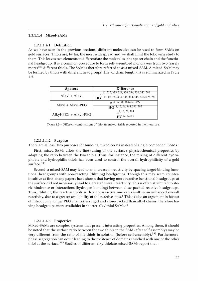
1.2. Chemical functionalizations of gold and silica
1.2.1.1.4 Mixed-SAMs
1.2.1.1.4.1 DefinitionAs we have seen in the previous sections, different molecules can be used to form SAMs ongold surfaces. Thiols are, by far, the most widespread and we shall limit the following study tothem. This leaves two elements to differentiate the molecules : the spacer chain and the functio-nal headgroup. It is a common procedure to form self-assembled monolayers from two (rarelymore)387 different thiols. The SAM is therefore referred to as a mixed-SAM. A mixed-SAM maybe formed by thiols with different headgroups (HG) or chain length (n) as summarized in Table1.5.
Spacers Difference
Alkyl + Alkyln11, 323, 325, 329, 330, 334, 336, 342, 388
HG1, 11, 12, 320, 334, 336, 344, 345, 347, 389, 390
Alkyl + Alkyl-PEGn11, 12, 26, 364, 391, 392
HG11, 12, 26, 364, 391, 392
Alkyl-PEG + Alkyl-PEGn2, 16, 26, 364
HG2, 16, 364
Table 1.5 – Different combinations of thiolate mixed-SAMs reported in the literature.
1.2.1.1.4.2 PurposeThere are at least two purposes for building mixed-SAMs instead of single-component SAMs :
First, mixed-SAMs allow the fine-tuning of the surface’s physicochemical properties byadapting the ratio between the two thiols. Thus, for instance, the mixing of different hydro-phobic and hydrophilic thiols has been used to control the overall hydrophilicity of a goldsurface.333
Second, a mixed-SAM may lead to an increase in reactivity by spacing target-binding func-tional headgroups with non-reacting (diluting) headgroups. Though this may seem counter-intuitive at first, many papers have shown that having more reactive functional headgroups atthe surface did not necessarily lead to a greater overall reactivity. This is often attributed to ste-ric hindrance or interactions (hydrogen bonding) between close-packed reactive headgroups.Thus, diluting the reactive thiols with a non-reactive one can result in an enhanced overallreactivity, due to a greater availability of the reactive sites.1 This is also an argument in favourof introducing longer PEG chains (less rigid and close-packed than alkyl chains, therefore ha-ving headgroups more available) in shorter alkylthiol SAMs.11
1.2.1.1.4.3 PropertiesMixed-SAMs are complex systems that present interesting properties. Among them, it shouldbe noted that the surface ratio between the two thiols in the SAM (after self-assembly) may bevery different from the ratio of the thiols in solution (before self-assembly).393 Furthermore,phase segregation can occur leading to the existence of domains enriched with one or the otherthiol at the surface.393 Studies of different alkylthiolate mixed-SAMs report that :
33
Chapter 1. State of the art
– For methyl-terminated thiols, phase segregation occurs in ethanol when the difference inchain lengths exceeds a certain value Nmin which depends on the temperature. At roomtemperatureNmin ≈ 4 while at 50◦CNmin ≈ 8.331, 342 Furthermore, phase segregation mayoccur as a function of the solvent if both molecules are not solvated equally.393
– Concerning thiols with same length but different headgroups, reports of MUA/C9-CH3and MUA/11-mercapto-1-undecanol (MUOH) mixed-SAMs in ethanol show that the sur-face ratio of both thiols is generally in good agreement with the solution ratio, as eviden-ced by XPS320, 336, 344, 390 and PM-IRRAS.336, 344, 389
– Phase segregation does not seem to occur between co-adsorbed MUA/MUOH,344 MUA/C11-CH3345 or MUOH/C11-CH3 in ethanol.345 However in the last two examples, whenmixed-SAMs were prepared by a gradient immersion followed by back-filling, differentdomains appeared.345
– Moreover, relationship between the binding efficiency of mixed-SAMs and their compo-sition is a matter of debate. Haussling et al.394 used biotinylated-thiol/MUOH mixed-SAMs at different ratios and found a much greater streptavidin binding on the least bio-tinylated SAMs. They attributed this to the greater spacing between biotin headgroupsthat should minimize steric hindrance for biorecognition. As we will see in the results ofthis thesis, our results do not suggest the same as we achieved high streptavidin bindingwith a pure biotinylated SAM. The binding efficiency in our case was not improved bySAM dilution. In another report on mixed-SAMs reactivity334 it is suggested that somemixed-SAMs may lead to a greater binding of a given protein albeit with a lower amountof subsequent biorecognition by a further antibody.
Given the above-mentioned comments on reported works on mixed-SAMs it seems reaso-nable to say that a general consensus on mixed-SAMs composition, structuration and speciallyreactivity has not been reached. Moreover, concerning reactivity towards proteins, given thecomplexity of the latter, it is possible that optimum conditions of the mixed-SAMs might notapply from one study to another (from one protein to another). We can rather imply that suchoptimization should be made for each precise case, that is for each precise biological test.
1.2.1.2 Different protocols
So far we have seen that a great diversity of thiols can be used to build SAMs on gold but wehave not mentioned how this functionalization can be achieved. In the following paragraphswe will briefly summarize different protocols reported in the literature to build these SAMsfrom a liquid or gas phase.
1.2.1.2.1 From solution
An easy way to form thiolate SAMs on a gold surface is to immerse the sample (goldsubstrate) into a liquid solvent containing the desired thiols at room temperature. The mostcommon solvent to form SAMs from alkylthiols as well as PEG-thiols is pure ethanol, al-though other solvents are also reported such as water/ethanol mixture,19, 314 THF,390, 395 chlo-roform,356 DiMethylFormamide (DMF),314, 395 hexadecane,395 carbon tetrachloride (CCl4),314, 395
DiChloroMethane (DCM),356 diethyl ether,356 cyclooctane,395 toluene,395 acetonitrile,314, 356, 395
ethyl acetate,356 bicyclohexyl396 and even a pure thiol liquid.395 Reports on the use of differentsolvents314, 395 show that SAMs can be formed from all of the above. Whether one is prefe-rable to another seems to depend on which molecule is used for the SAM as well as which
34
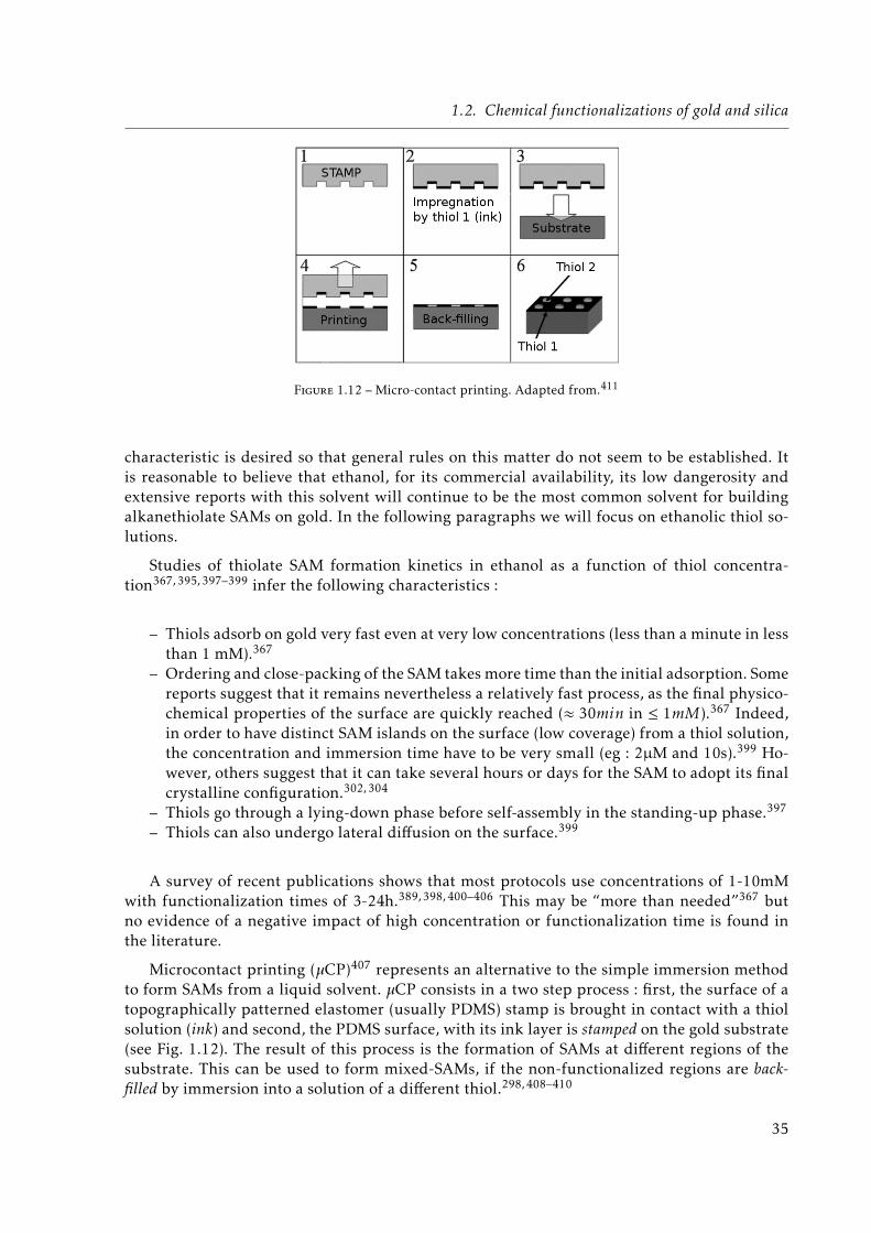
1.2. Chemical functionalizations of gold and silica
Figure 1.12 – Micro-contact printing. Adapted from.411
characteristic is desired so that general rules on this matter do not seem to be established. Itis reasonable to believe that ethanol, for its commercial availability, its low dangerosity andextensive reports with this solvent will continue to be the most common solvent for buildingalkanethiolate SAMs on gold. In the following paragraphs we will focus on ethanolic thiol so-lutions.
Studies of thiolate SAM formation kinetics in ethanol as a function of thiol concentra-tion367, 395, 397–399 infer the following characteristics :
– Thiols adsorb on gold very fast even at very low concentrations (less than a minute in lessthan 1 mM).367
– Ordering and close-packing of the SAM takes more time than the initial adsorption. Somereports suggest that it remains nevertheless a relatively fast process, as the final physico-chemical properties of the surface are quickly reached (≈ 30min in ≤ 1mM).367 Indeed,in order to have distinct SAM islands on the surface (low coverage) from a thiol solution,the concentration and immersion time have to be very small (eg : 2µM and 10s).399 Ho-wever, others suggest that it can take several hours or days for the SAM to adopt its finalcrystalline configuration.302, 304
– Thiols go through a lying-down phase before self-assembly in the standing-up phase.397
– Thiols can also undergo lateral diffusion on the surface.399
A survey of recent publications shows that most protocols use concentrations of 1-10mMwith functionalization times of 3-24h.389, 398, 400–406 This may be “more than needed”367 butno evidence of a negative impact of high concentration or functionalization time is found inthe literature.
Microcontact printing (µCP)407 represents an alternative to the simple immersion methodto form SAMs from a liquid solvent. µCP consists in a two step process : first, the surface of atopographically patterned elastomer (usually PDMS) stamp is brought in contact with a thiolsolution (ink) and second, the PDMS surface, with its ink layer is stamped on the gold substrate(see Fig. 1.12). The result of this process is the formation of SAMs at different regions of thesubstrate. This can be used to form mixed-SAMs, if the non-functionalized regions are back-filled by immersion into a solution of a different thiol.298, 408–410
35
Chapter 1. State of the art
1.2.1.2.2 From gas phase
Thiolate SAMs can also be formed by adsorption from a gas phase in ultrahigh vacuum.303, 412
This method is not as widely used as the adsorption from a liquid phase though, as it is moredifficult to implement and often yields less densely packed SAMs.302 However, adsorption froma gas phase has been used to obtain fundamental information about the SAM formation me-chanisms and kinetics, specially at the early stages. Some of the fundamental characteristicsthat will be detailed in section 1.2.1.3.2 could only be evidenced by formation from an Ul-trahigh Vacuum (UHV) gas phase. Furthermore, from an UHV phase, there is no competingsolvent-substrate or solvent-thiols interactions which can hinder the formation of the SAM.302
1.2.1.3 Summary and main characteristics of SAMs on gold
As we have seen in the previous paragraphs, gold surfaces can be functionalized with manydifferent SAMs (see section 1.2.1.1) formed in different conditions (see section 1.2.1.2). Howe-ver, since the introduction of these systems, some choices have been much more widely spreadand become a sort of “standard”. In the following paragraphs we will summarize these com-mon choices and give some fundamental characteristics about the so-formed SAMs.
1.2.1.3.1 Towards a standard protocol for gold functionalization
From the comments and number of cited papers in sections 1.2.1.1 and 1.2.1.2 we canconclude that for most applications requiring gold functionalization (specially in biosensingtechnology) SAMs are formed from adsorption of thiols in ethanol at a concentration of around1-10 mM during 3-10 h. These thiols usually have an alkyl or alkyl-PEG (specially for anti-fouling) spacer with common lengths of around 6-16 methylene units (10, 11 and 16 beingspecially common) and 3-6 Ethylene Glycol (EG) units in the case of alkyl-PEGs. The mostcommon headgroups for biosensing applications are COOH (often activated by NHS-ester)and NH2 for biomolecule binding and OH and CH3 for anti-fouling. Eventually, mixed-SAMsare also widely used, often combining a target-binding thiol and a diluting one to separate thereactive sites at the surface. These are commonly formed by two alkylthiols or an alkylthioland a PEG-thiol.
Obviously, this short summary does not mean that all the other alternatives cited in theprevious sections do not deserve our attention but for reasons that probably include simpli-city, previous knowledge and experience as well as economic cost, these are the most commonchoices made for gold functionalization.
1.2.1.3.2 Characteristics of thiolate SAMs on Au(111)
So far we have adopted a rather “practical” point of view and not discussed in much detailthe most fundamental aspects of SAM formation. However, questions such as what is the natureof the Gold-SAM bond ? what is the nature and kinetics of the intermolecular forces that drive theformation of a close-packed SAM ? or what are the SAMs’ most common defects and how do they relateto the substrate’s characteristics ? have been and still are a matter of active research302, 413–423
that we shall briefly summarize in the following paragraphs. We shall limit this study to SAMsformed by alkylthiols on Au(111) substrates, which is the most commonly obtained orientationby methods such as e-beam evaporation.
36
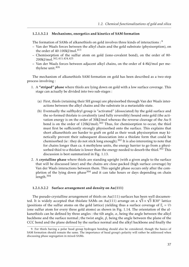
1.2. Chemical functionalizations of gold and silica
1.2.1.3.2.1 Mechanisms, energetics and kinetics of SAM formation
The formation of SAMs of alkanethiols on gold involves three kinds of interactions : 9
– Van der Waals forces between the alkyl chain and the gold substrate (physisorption), onthe order of 40-100kJ/mol.413
– Chemisorption of the sulfur atom on gold (iono-covalent bond), on the order of 80-200kJ/mol.302, 413, 424, 425
– Van der Waals forces between adjacent alkyl chains, on the order of 4-8kJ/mol per me-thylene unit.426
The mechanism of alkanethiols SAM formation on gold has been described as a two-stepprocess involving :
1. A “striped” phase where thiols are lying down on gold with a low surface coverage. Thisstage can actually be divided into two sub-stages :
(a) First, thiols (retaining their SH group) are physisorbed through Van der Waals inter-actions between the alkyl chains and the substrate in a metastable state.
(b) Eventually the sulfhydryl group is “activated” (dissociated) by the gold surface andthe so-formed thiolate is covalently (and fully reversibly) bound onto gold (the acti-vation energy is on the order of 30kJ/mol whereas the reverse cleavage of the Au-Sbond is on the order of 120kJ/mol).302 Thus, for chemisorption to occur, the thiolmust first be sufficiently strongly physisorbed onto the surface. This explains thatshort alkanethiols are harder to graft on gold as their weak physisorption may ki-netically prevent their subsequent dissociation into a thiolate form that could bechemisorbed (ie : they do not stick long enough).302 It is also interesting to note thatfor chains longer than ca. 6 methylene units, the energy barrier to go from a physi-sorbed thiol to a thiolate is lower than the energy needed to desorb the thiol.302 Thisdiscussion is best summarized in Fig. 1.13.
2. A crystalline phase where thiols are standing upright (with a given angle to the surfacethat will be discussed later) and the chains are close-packed (high surface coverage) byVan der Waals interactions between them. This upright phase occurs only after the com-pletion of the lying down phase304 and it can take hours or days depending on chainlength.304
1.2.1.3.2.2 Surface arrangement and density on Au(111)
The pseudo-crystalline arrangement of thiols on Au(111) surfaces has been well documen-ted. It is widely accepted that thiolate SAMs on Au(111) arrange on a
√3 × √3 R30◦ lattice
(positions of the sulfur atoms on the gold lattice) yielding thus a surface coverage of Γs = 1/3(one sulfur atom for every three gold atoms) as shown in Fig. 1.14. The orientation of the al-kanethiols can be defined by three angles : the tilt angle, α, being the angle between the alkylbackbone and the surface normal ; the twist angle, β, being the angle between the plane of theCCC bond and the plane defined by the surface normal and the alkyl backbone and finally the
9. For thiols having a polar head group hydrogen bonding should also be considered, though the basics ofSAM formation should remain the same. The importance of head group’s polarity will rather be addressed whendiscussing phase segregation in mixed-SAMs.
37
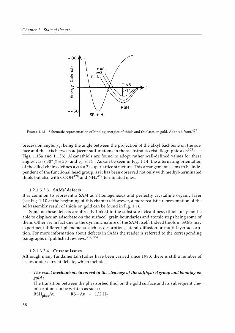
Chapter 1. State of the art
Figure 1.13 – Schematic representation of binding energies of thiols and thiolates on gold. Adapted from.427
precession angle, χt, being the angle between the projection of the alkyl backbone on the sur-face and the axis between adjacent sulfur atoms in the susbstrate’s cristallographic axis303 (seeFigs. 1.15a and 1.15b). Alkanethiols are found to adopt rather well-defined values for theseangles : α ≈ 30◦ β ≈ 55◦ and χt ≈ 14◦. As can be seen in Fig. 1.14, the alternating orientationof the alkyl chains defines a c(4×2) superlattice structure. This arrangement seems to be inde-pendent of the functional head group, as it has been observed not only with methyl-terminatedthiols but also with COOH428 and NH2
429 terminated ones.
1.2.1.3.2.3 SAMs’ defectsIt is common to represent a SAM as a homogeneous and perfectly crystalline organic layer(see Fig. 1.10 at the beginning of this chapter). However, a more realistic representation of theself-assembly result of thiols on gold can be found in Fig. 1.16.
Some of these defects are directly linked to the substrate : cleanliness (thiols may not beable to displace an adsorbate on the surface), grain boundaries and atomic steps being some ofthem. Other are in fact due to the dynamic nature of the SAM itself. Indeed thiols in SAMs mayexperiment different phenomena such as desorption, lateral diffusion or multi-layer adsorp-tion. For more information about defects in SAMs the reader is referred to the correspondingparagraphs of published reviews.302, 304
1.2.1.3.2.4 Current issuesAlthough many fundamental studies have been carried since 1983, there is still a number ofissues under current debate, which include :
– The exact mechanisms involved in the cleavage of the sulfhydryl group and bonding ongold :The transition between the physisorbed thiol on the gold surface and its subsequent che-misorption can be written as such :RSHphysAu RS−Au + 1/2 H2
38
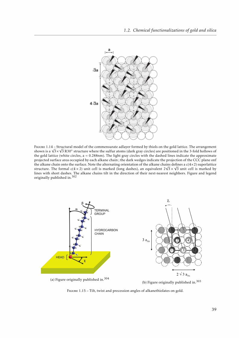
1.2. Chemical functionalizations of gold and silica
Figure 1.14 – Structural model of the commensurate adlayer formed by thiols on the gold lattice. The arrangementshown is a
√3×√3 R30◦ structure where the sulfur atoms (dark gray circles) are positioned in the 3-fold hollows of
the gold lattice (white circles, a = 0.288nm). The light gray circles with the dashed lines indicate the approximateprojected surface area occupied by each alkane chain ; the dark wedges indicate the projection of the CCC plane onfthe alkane chain onto the surface. Note the alternating orientation of the alkane chains defines a c(4×2) superlatticestructure. The formal c(4 × 2) unit cell is marked (long dashes), an equivalent 2
√3 × √3 unit cell is marked by
lines with short dashes. The alkane chains tilt in the direction of their next-nearest neighbors. Figure and legendoriginally published in.302
(a) Figure originally published in.304(b) Figure originally published in.303
Figure 1.15 – Tilt, twist and precession angles of alkanethiolates on gold.
39
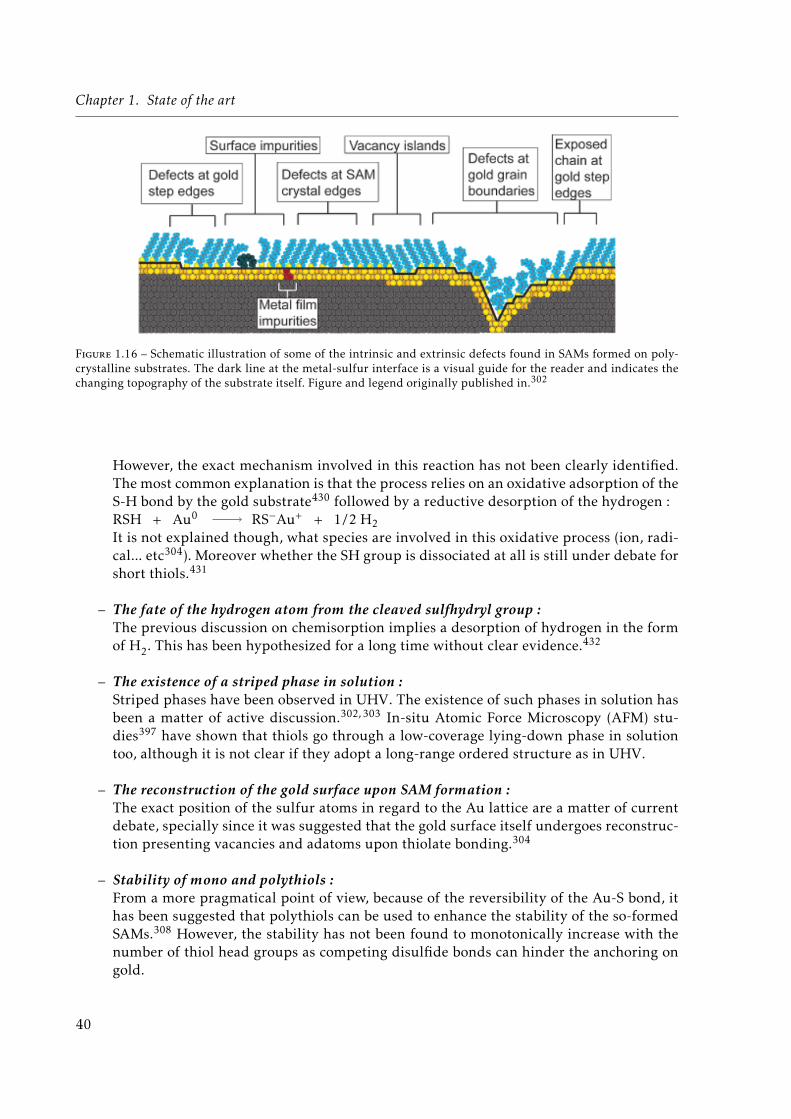
Chapter 1. State of the art
Figure 1.16 – Schematic illustration of some of the intrinsic and extrinsic defects found in SAMs formed on poly-crystalline substrates. The dark line at the metal-sulfur interface is a visual guide for the reader and indicates thechanging topography of the substrate itself. Figure and legend originally published in.302
However, the exact mechanism involved in this reaction has not been clearly identified.The most common explanation is that the process relies on an oxidative adsorption of theS-H bond by the gold substrate430 followed by a reductive desorption of the hydrogen :RSH + Au0 RS−Au+ + 1/2 H2It is not explained though, what species are involved in this oxidative process (ion, radi-cal... etc304). Moreover whether the SH group is dissociated at all is still under debate forshort thiols.431
– The fate of the hydrogen atom from the cleaved sulfhydryl group :The previous discussion on chemisorption implies a desorption of hydrogen in the formof H2. This has been hypothesized for a long time without clear evidence.432
– The existence of a striped phase in solution :Striped phases have been observed in UHV. The existence of such phases in solution hasbeen a matter of active discussion.302, 303 In-situ Atomic Force Microscopy (AFM) stu-dies397 have shown that thiols go through a low-coverage lying-down phase in solutiontoo, although it is not clear if they adopt a long-range ordered structure as in UHV.
– The reconstruction of the gold surface upon SAM formation :The exact position of the sulfur atoms in regard to the Au lattice are a matter of currentdebate, specially since it was suggested that the gold surface itself undergoes reconstruc-tion presenting vacancies and adatoms upon thiolate bonding.304
– Stability of mono and polythiols :From a more pragmatical point of view, because of the reversibility of the Au-S bond, ithas been suggested that polythiols can be used to enhance the stability of the so-formedSAMs.308 However, the stability has not been found to monotonically increase with thenumber of thiol head groups as competing disulfide bonds can hinder the anchoring ongold.
40
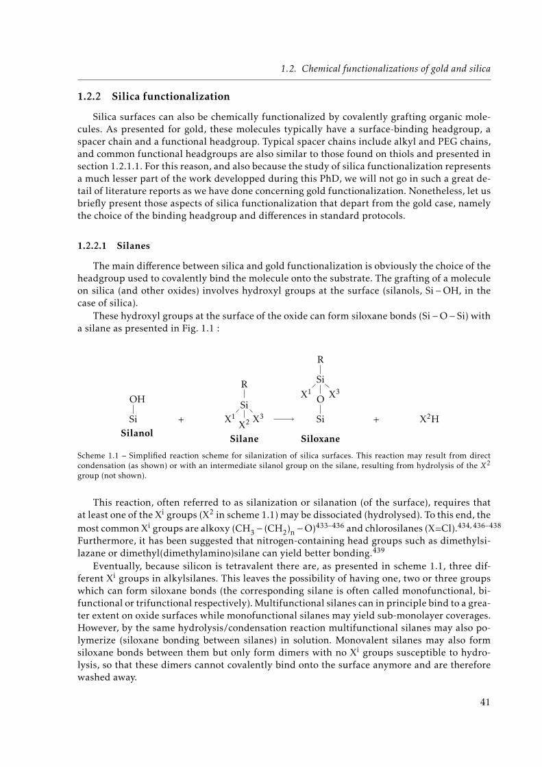
1.2. Chemical functionalizations of gold and silica
1.2.2 Silica functionalization
Silica surfaces can also be chemically functionalized by covalently grafting organic mole-cules. As presented for gold, these molecules typically have a surface-binding headgroup, aspacer chain and a functional headgroup. Typical spacer chains include alkyl and PEG chains,and common functional headgroups are also similar to those found on thiols and presented insection 1.2.1.1. For this reason, and also because the study of silica functionalization representsa much lesser part of the work developped during this PhD, we will not go in such a great de-tail of literature reports as we have done concerning gold functionalization. Nonetheless, let usbriefly present those aspects of silica functionalization that depart from the gold case, namelythe choice of the binding headgroup and differences in standard protocols.
1.2.2.1 Silanes
The main difference between silica and gold functionalization is obviously the choice of theheadgroup used to covalently bind the molecule onto the substrate. The grafting of a moleculeon silica (and other oxides) involves hydroxyl groups at the surface (silanols, Si−OH, in thecase of silica).
These hydroxyl groups at the surface of the oxide can form siloxane bonds (Si−O− Si) witha silane as presented in Fig. 1.1 :
Si
OH
Silanol+ X1
Si
X2 X3
R
Silane
Si
O
Si
X1 X3
R
Siloxane
+ X2H
Scheme 1.1 – Simplified reaction scheme for silanization of silica surfaces. This reaction may result from directcondensation (as shown) or with an intermediate silanol group on the silane, resulting from hydrolysis of the X2
group (not shown).
This reaction, often referred to as silanization or silanation (of the surface), requires thatat least one of the Xi groups (X2 in scheme 1.1) may be dissociated (hydrolysed). To this end, themost common Xi groups are alkoxy (CH3 − (CH2)n −O)433–436 and chlorosilanes (X=Cl).434, 436–438
Furthermore, it has been suggested that nitrogen-containing head groups such as dimethylsi-lazane or dimethyl(dimethylamino)silane can yield better bonding.439
Eventually, because silicon is tetravalent there are, as presented in scheme 1.1, three dif-ferent Xi groups in alkylsilanes. This leaves the possibility of having one, two or three groupswhich can form siloxane bonds (the corresponding silane is often called monofunctional, bi-functional or trifunctional respectively). Multifunctional silanes can in principle bind to a grea-ter extent on oxide surfaces while monofunctional silanes may yield sub-monolayer coverages.However, by the same hydrolysis/condensation reaction multifunctional silanes may also po-lymerize (siloxane bonding between silanes) in solution. Monovalent silanes may also formsiloxane bonds between them but only form dimers with no Xi groups susceptible to hydro-lysis, so that these dimers cannot covalently bind onto the surface anymore and are thereforewashed away.
41
Chapter 1. State of the art
1.2.2.2 Protocols
As in gold functionalization, silanization is usually carried out by immersing the samplesurface into a dilute solution of silanes in an organic solvent. However the choice of the solventand experimental conditions is somehow more delicate than for thiols on gold because of thecompeting hydrolysis/condensation of silanes in solution (polymerization) as already men-tioned. Organic solvents used for silanization include : toluene,435, 437, 438, 440, 441 ethanol,433
xylene,439 pentane,441 bicyclohexyl,396 acetone,442, 443 CCl4,439, 441 benzene,441 cyclooctane,441
hexadecane,441 octane,441 cyclohexane,441 hexane,441 dioxane441 and dichloromethane.441
These solvents are either dried,440 used in normal conditions (neither dried nor mixed withadded water) or mixed with ultrapure water.442, 443 Additional curing steps are sometimes un-dertaken, heating the sample above 100◦C for cross-linking of the layer.439, 440
In order to partly circumvent some of these issues, silanization from a gas phase has alsobeen investigated.444, 445
1.2.2.3 Summary and main characteristics of SAMs on silica
Given the large differences in reported protocols of silanization, it is reasonable to concludethat this process is somehow more complex than gold functionalization with thiols due to thepossible siloxane bonding of silanes in solution leading to polymerization (multifunctional si-lanes) or dimerization (monofunctional silanes). Indeed, it seems that the amount of water, thetemperature, the hydroxylation of the surface and the nature of the silane (specially monofunc-tional vs polyfunctional) can affect the formation and stability of the organic layer. However,how exactly each of these parameters affect the final result is still a matter of debate.439
1.2.3 Chemical characterization
There are several tools to probe the chemistry of self-assembled monolayers at a solid sur-face. These can roughly be separated by the kind of information that they provide : 10
1. Average information on the physicochemical properties of the surface (e.g., surface chargeor hydrophilicity).
2. Average chemical and structural composition of the organic layer (e.g., ratio of differentmolecules in mixed-SAMs or general degree of hydrogen bonding between headgroups).
3. Local information about the layer composition and organization (e.g., phase segregationin mixed-SAMs or pinhole defects).
It is not the purpose of this section to give extensive details about these techniques but ratherto understand what kind of information can be obtained by them. Of all the following tools,only those that were used to obtain the results presented in this manuscript will be explainedin more detail in the next chapter and corresponding appendixes.
10. Depending on the use that is made of each of these tools, different informations can be obtained which, ofcourse, make this separation somehow questionable. However it is obvious that some tools are better suited forobtaining some information than others and it is in this “general” case of “standard” use of the tools that thisclassification is made.
42
1.2. Chemical functionalizations of gold and silica
1.2.3.1 General physicochemical properties (“macroscopic methods”)
This section quickly describes macroscopic methods for the characterization of SAMs onhomogeneous planar surfaces. These methods do not give direct chemical information aboutthe surface but rather physical properties such as wettability, thickness or electrical behaviourof the SAM, which have to be linked to the chemical composition under some assumptions.The SAMs considered here are typically formed from small organic molecules (chain lengthof around 10 methylene units). For bigger molecules, other methods commonly employed inbiosensing technology such as Surface Plasmon Resonance (SPR)446 or Quartz Crystal Micro-balance (QCM)335 may be used.
1.2.3.1.1 Contact angle
The contact angle of a liquid drop with a surface directly translates the surface wettability(hydrophilicity in the case of water), which can be related to the presence and composition of aSAM. Thus, contact angle measurements (goniometry) are usually undertaken as a rapid meanto prove the success of the functionalization, followed by more in-depth characterizations suchas different spectroscopies.447–449
However, despite its apparent simplicity, careful examination of contact angle measure-ments have been used to determine important characteristics of SAMs, such as :
– The odd/even effect302, 360–362 that was previously discussed within the considerationsof the spacer chain lenghts in paragraph 1.2.1.1.2 and that suggests that alkanethiols ofdifferent lengths form SAMs with a well-defined tilt angle.
– The relative amount and mixing of different molecules in mixed-SAMs.450–453
– The effect of pH on the functional head group.405
– The effect of different parameters (time, solvent, concentration, substrate cleanliness) onSAM formation.395
1.2.3.1.2 Ellipsometry
Ellipsometry provides information about a thin film’s thickness (given its refractive index)which can be used as a method for SAM characterization. The most straightforward used ofthis method is to link the so-measured thickness to the chain length of the molecules. It cantherefore be used as a routine characterization to prove the formation of a SAM and check theabsence of adsorbed multi-layers.448 It can however also be used for more in-depth parametricinvestigations on SAM formation (as a function of time, concentration, solvent or substrate“cleanliness”).395
As contact angle goniometry, ellipsometry is however rarely used as the sole characteriza-tion method of a SAM but rather followed by some spectroscopy (XPS, Infrared (IR)) to probethe chemical composition of the surface in more detail.448, 449, 454, 455
Eventually, it should be noted that conducting ellipsometry measurements on typical SAMshaving a thickness of less than 2nm can be cumbersome as the potential errors on the measu-rements become close to the total measured thickness. As the values given by this techniquerely on the input model given for the layer that has to be characterized, they may be morequestionable than the values given by other direct techniques.
1.2.3.1.3 Electrochemistry
43
Chapter 1. State of the art
Electrochemistry -Cyclic Voltametry (CV) or Electrochemical Impedance Spectroscopy (EIS)-has been used to characterize alkanethiolate SAMs on gold. It is for instance possible to linkthe electronic (blocking) properties of the SAM to its thickness (thicker SAMs are obviouslyless conducting), its packing density or the presence and nature of defects.456
1.2.3.2 Average chemical and structural composition (spectroscopies)
Spectroscopy’s main advantage over the previously cited methods is that it provides relati-vely unambiguous information about the chemical composition of the surface. Different spec-troscopies are therefore widely used in the characterization of SAMs on planar substrates, thatwe shall briefly describe hereafter. From a spatial resolution point of view, these techniquescan be either macroscopic (the irradiated region -beam spot on the surface- being over 1mm2)or offer micrometric resolution if the beam can be focused on that scale.
1.2.3.2.1 Infrared spectroscopy
Infrared spectroscopy is based on the absorbtion of infrared photons by chemical bonds(excitation of different vibration modes). It is therefore very useful in determining the struc-ture of molecules grafted on a surface. Examples of typical bonds evidenced in SAMs throughIR spectroscopy include CH3, CH2, O = C−NH (amide), COOH, COO−, and C−OH. Further-more the exact position (excitation wavenumber) and shape of the peaks can yield valuableinformation about the environment of the molecule. For instance C = O vibration modes of ter-minal carboxylic acids have different positions depending on the hydrogen-bonding with anadjacent group.457–459 Similarly, CH2 vibration modes of alkyl chains shift with the presenceof an adjacent chain, so that the position of the peak can translate the degree of order andclose-packing in the SAM.335, 344, 460
PM-IRRAS is an important development of IR spectroscopy for probing metallic surfaces,which will be discussed in the next chapter and corresponding appendix.
1.2.3.2.2 Raman spectroscopy
Raman spectroscopy is similar to IR spectroscopy in the sense that it uses infrared radiationto excite vibration modes of chemical bonds. However, in Raman spectroscopy, the infraredphotons are scattered in an inelastic way (Stokes or anti-stokes scattering). Therefore somechemical groups may give a weaker or stronger signal in one or the other method. Surface-Enhanced Raman Spectroscopy (SERS) is an important development of Raman spectroscopythat can be very useful in the characterization of SAMs.461
Moreover, Tip-Enhanced Raman Spectroscopy (TERS) is a very promising technique alsobased on Raman spectroscopy, but we shall discuss its potential separately in section 1.2.3.3.
1.2.3.2.3 XPS
XPS is another widely used method for the characterization of SAMs. XPS probes the bin-ding energy of core-level electrons in atoms. Thus, it is in principle an elemental characteriza-tion tool as opposed to IR or Raman spectroscopies. However the exact values of these bindingenergies also depend on the surrounding electronic environment (chemical bonds in which thegiven atom takes part) ; i.e., the binding energy of 1s orbital of a carbon atom in an alkyl chain
44
1.2. Chemical functionalizations of gold and silica
(C1s level of C-C-C) is different than that of 1s orbital of a carbon atom in a PEG chain (C1slevel of C-C-O).19 Therefore, XPS is also used to determine the chemical composition of mole-cules on a surface. This explains that XPS is also known as Electron Spectroscopy for ChemicalAnalysis (ESCA).
1.2.3.2.4 ToF-SIMS
ToF-SIMS, whose principle will be detailed in the next chapter, is a very sensitive surfaceanalysis method that can be used to characterize SAMs and monitor its formation kinetics.462
1.2.3.3 Localized nanometric information (scanning probe microscopies)
Scanning probes microscopies, which could in fact be referred to as nanoscopies, are veryimportant in the investigation of self-assembled monolayers. With their nanometric spatialresolution, they are specially suited to investigate such questions as the mixing or phase se-gregation of molecules in mixed-SAMs or the existing of a lying-down low-coverage phase inself-assembly.
45

Chapter 1. State of the art
1.2.3.3.1 STM
Scanning Tunnelling Microscopy (STM) has been widely used to study alkanethiolate SAMson gold.321, 322, 325–327, 331, 340, 354, 378, 463, 464 The use of STM has specially been crucial in earlyfundamental studies of SAM formation showing evidence of different low-coverage and high-coverage phases and crystalline arrangements as well as defects both in one-component andbinary (mixed) SAMs. A review entirely devoted to such investigations by STM was publishedin 1997 by Gregory E. Poirier.412 STM remains a reference tool nowadays for investigation ofmore complex SAMs.465
1.2.3.3.2 AFM
AFM might be the most widespread scanning probe microscopy. A reason for this is thatit can work on very different materials, unlike STM which requires a conducting substratefor instance, and under different conditions (vacuum, air or liquid). AFM has been used inthe past and is still widely used to characterize different SAMs.331, 332, 335, 466, 467 The in-situevidence of low-coverage phases during thiolate SAM formation from solution is an exampleof an important contribution by AFM measurements to the knowledge of SAM formation.397
As a consequence of AFM versatility, there have been numerous variations of the standardAFM, that correspond to different functionalities of the tip such as Piezoelectric Force Micro-scopy (PFM) or Magnetic Force Microscopy (MFM). Among them, Chemical Force Microscopy(CFM) -not to be mistaken with Conductive Atomic Force Microscopy (C-AFM)- is speciallyinteresting for probing surface functionalization.468
1.2.3.3.3 TERS
In a nutshell, TERS is the combination of Raman Spectroscopy and AFM. Indeed, in a TERSexperiment, a far-field beam is coupled to a local probe (modified AFM tip) to irradiate only asmall region (down to ca. 10nm x 10nm) of the surface that will provide a Raman signal. Thistechnique is very promising as it combines the best of both worlds : unique spatial resolutionwith unique spectral signatures for identification of different molecules. A remarkable exampleby Stadler et al.410 shows how TERS can clearly distinguish domains of different thiolate iso-mers deposited on a surface through microcontact-printing and back-filling. TERS is a ratherrecent method which requires very careful considerations in the tip and setup design.469
1.2.3.4 Summary of characterization methods
The aforementioned techniques are summarized with some of their characteristics in Table1.6. The values given in this table are obviously only indicative and do not reflect all the com-plexity of each method, whose performances may vary depending on different parameters suchas the precise device technical characteristics or the exact material being probed.
46
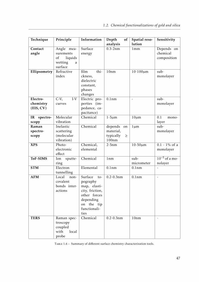
1.2. Chemical functionalizations of gold and silica
Technique Principle Information Depth ofanalysis
Spatial reso-lution
Sensitivity
Contactangle
Angle mea-surementsof liquidswetting asurface
Surfaceenergy
0.3-2nm 1mm Depends onchemicalcomposition
Ellipsometry Refractiveindex
film thi-ckness,dielectricconstant,phaseschanges
10nm 10-100µm sub-monolayer
Electro-chemistry(EIS, CV)
C-V, I-Vcurves
Electric pro-perties (im-pedance, ca-pacitance)
0.1nm - sub-monolayer
IR spectro-scopy
Molecularvibration
Chemical 1-5µm 10µm 0.1 mono-layer
Ramanspectro-scopy
Inelasticscattering(molecularvibration)
Chemical depends onmaterial,typically ≥100nm
1µm sub-monolayer
XPS Photo-electroniceffect
Chemical,elemental
2-5nm 10-50µm 0.1 - 1% of amonolayer
ToF-SIMS Ion sputte-ring
Chemical 1nm sub-micrometer
10−5 of a mo-nolayer
STM Electrontunnelling
Elemental 0.1nm 0.1nm -
AFM Local non-covalentbonds inter-actions
Surface to-pographymap, elasti-city, friction,other forcesdependingon the tipfunctionali-ties
0.2-0.3nm 0.1nm -
TERS Raman spec-troscopycoupledwith localprobe
Chemical 0.2-0.3nm 10nm -
Table 1.6 – Summary of different surface chemistry characterization tools.
47
Chapter 1. State of the art
1.3 Orthogonal functionalizations of heterogenous substrates andits applications
1.3.1 Introduction to orthogonal functionalizations
Building SAMs on plain gold and silica surfaces is now a rather common procedure knownfor a few decades (though some fundamental questions are still open to debate and optimalconditions or “standard protocols” -specially for silanization- have not been clearly shown).However, in many nanotechnology fields such as biosensing, the current trend leads to com-plex devices with heterogeneous (patterned) surfaces. Periodic gold nanostructres on a silicasurface, for instance, can serve as an Localized Surface Plasmon Resonance (LSPR)-based bio-sensor.470 The main challenge from a functionalization point of view is thus to achieve thebuilding of different SAMs selectively onto the different materials at the surface. This processhas been designated as orthogonal functionalizations302 or site-selective patterning471 in the lite-rature. 11
1.3.2 Reported examples of orthogonal functionalizations
Gold structures on silica (or other metallic structures on oxide) is quite a common case as itmay have different applications in optics and electronics. Different uses of orthogonal functio-nalization on these patterned substrates can be found in the literature. We will briefly presentsome of them hereafter :
– Laibinis et al.472 were the first, to the best of our knowledge, to present orthogonal func-tionalizations of micropatterned gold/oxyde surfaces.
– Our group reported the use of MUA and PEG-silane on patterned gold on glass (mil-limetric patterning) for the selective binding of magnetic bead filaments onto the goldregions.299
– Pradier and co-workers442 worked on 100µm diameter SiO2 areas surrounded by gold.The silica regions were biotinylated while the surrounding gold was rendered inert withOEG. This allowed specific binding of streptavidin onto the silica regions, followed bybiotinylated anti-rIgG. Eventually, the specificity of bio-recognition onto the silica re-gions was monitored by fluorescence (targets were fluorescently labeled). Though discar-ded in the article, it is however reasonable to question the lack of fluorescence quenchingon possibly adsorbed targets on gold.
– Udo Bach and co-workers27, 300, 473, 474 used orthogonal functionalizations for the nano-metric precise placement of gold colloids. Using thiolated DeoxyriboNucleic Acid (DNA)and PEG-silanes, they achieved almost single-particle capture with 40nm beads and lessthan 1% of non-specific adsorption (beads adsorbed on silica surrounding gold nano-structures) on millimetric overall surfaces.27 This methodology, combined with elec-
11. From the given references, orthogonal functionalization designates a broader concept including the buildingof different self-assembled monolayers on a homogeneous substrate (eg : through micro-contact printing and back-filling). However, unless otherwise specified we will refer only to heterogeneous substrates with material-selectivefunctionalizations.
48
1.3. Orthogonal functionalizations of heterogenous substrates and its applications
trostatic interactions between DNA-modified beads and aminofunctionalized gold, wasused to develop a complex “Gutenberg-style printing of Self-Assembled Nanoparticle Ar-rays”.300
– Yutaka Majima and co-workers475–477 used dithiols to bind gold nanoparticles on thegap between two gold electrodes. This methodology is surprising, since it relies on thefact that the dithiols will bind onto the colloid particle and onto the electrode, insteadof binding by both endgroups onto the same surface. In fact, the dithiols were insertedinto previously thiol SAMs on the electrodes, which may explain that one of the thiolextremities remained free to bind the colloidal particle instead of having the dithiol bindtwice onto the electrode. Anyhow, they achieved single particle capture on the gap of theelectrodes, which resulted in the realization of a Single Electron Transistor (SET) ; wherethe colloidal gold particle behaves as a Coulomb island. This work, however did not usefunctionalizations on the surrounding surface to limit non-specific adsorption.
– Höök and co-workers28, 478, 479 used orthogonal functionalizations of Au/SiO2 and Au/TiO2patterns to enhance the sensitivity of LSPR biosensors. They modified gold and oxide sur-faces with an SH-PEG and Poly-L-Lysine (PLL)-g-PEG respectively, each of which couldbe biotinylated or not. Depending on which PEG beared a biotin moiety, they couldcontrol the binding of NeutrAvidin onto one or the other material, demonstrating theenhanced sensitivity of the sensor when gold was rendered “bioactive” (biotinylated).
– With the same functionalization (SH-PEG(-biotin) and PLL-g-PEG) and nitrodopamin-PEG-biotin (to bind onto TiO2 via the catechol group), Zhang et al.480 achieved strepta-vidin localization at the hotspots of plasmonic nano-antennas.
– In a similar, though simpler (and somehow more questionable) approach, Kumar et al.29
adsorbed PLL-g-PEG on a patterned silicon nitride / gold surface, followed by strepta-vidin immobilization which according to the authors is meant to replace the PLL-g-PEGon the gold regions while having no effect on the silicon nitride regions. Though this as-sumption is questionable, the authors report it as a mean to localize biotinylated vesiclesinto LSPR supporting gold regions.
1.3.3 Conclusions and perspectives of orthogonal functionalizations
As we can see from this literature survey, the orthogonal functionalizations of patternedgold on silica (or other oxides) has already been undertaken by a few groups throughout theworld. It seems that this methodology is gaining importance since 2010. Indeed, the articles ofLalander et al.27 and Feuz et al.28 in ACS Nano are very good examples of the issue presentedin this thesis. Both show how orthogonal functionalizations can be used either for the preciseplacement of colloids27 or the enhancement of LSPR-based biosensor with selective captureof target proteins on sensitive areas.28 Despite further improvements since 2010,300, 473, 474, 479
a number of points can still be raised, which, to the best of our knowledge are not yet fullyanswered in the literature :
49
Chapter 1. State of the art
1. Direct chemical characterization : Most of the examples presented above lack direct che-mical characterization of the functionalization step. This means that the measurementsare taken at the end of the process, involving colloid deposition (assessed by SEM for ins-tance) or SPR signal reading. The problem with such “end of process measurements” isthat it is difficult to explain some of the results and point out which step may have failedand to what extent. For instance, in the work of Feuz et al.,28 the authors observe an SPRsignal even when only the non-sensitive oxide regions are meant to be bio-functionalized.In this case, in the absence of chemical characterization at the functionalization step, it isimpossible to know if this signal is due to an imperfect orthogonal functionalization or tonon-specific adsorption of target biomolecules (on a perfectly functionalized substrate).It is reasonable to think that in that precise case28 (and even more so on the paper by Ku-mar et al.29 as previously explained) the chemical functionalization may have not beenperfectly orthogonal, as the PLL-g-PEG used may have adsorbed on bare or functionali-zed gold as well as on TiO2, which brings us to the second point.
2. Selective attachment layers : It is obviously important to achieve functionalizations thatare truly orthogonal. This means that the two molecules used should be highly selectivetowards one or the other material. It also means that washing steps may play a crucialrole in removing non-specifically adsorbed molecules.
3. Single-step functionalizations : To the best of our knowledge, all the so-far reportedorthogonal functionalizations involve two steps : functionalization of one material (+washing) followed by functionalization of the second material. However, if functionali-zations are truly orthogonal (material-selective), there is no reason why both functiona-lizations could not be operated simultaneously. This would greatly simplify the process,which in general is already complex if one takes into account all the steps from top-downfabrication to the final biological test.
4. Thin attachment layers : Moreover, for sensors based on evanescent waves (SPR), it isimportant that the final target be as close to the surface as possible. As such, it is impor-tant to develop chemical functionalizations with small molecules (few nm ; few hundredsg/mol) instead of -big- polymers or other macromolecules (2-3 kg/mol).28
5. Diversity : Obviously, even if we restrict ourselves to the orthogonal functionalizations ofone kind of substrate (patterned gold on silica) there are infinite possibilities that are yetto be explored, regarding the functionalization itself as well as the applications. Udo Bachand co-workers27 nicely presented the localization of gold colloids based on orthogonalfunctionalizations, but the use of latex beads, possibly with added functionalities such asmagnetic or fluorescent properties can be an interesting branching of this methodology,specially if these beads are placed on active regions of a surface (eg : electrodes, plasmo-nic antennas or microcantilevers). Similarly, the group of Höök and co-workers28 usedorthogonal functionalizations on LSPR biosensors to detect NeutrAvidin on biotinylatedsurfaces. Yet, with slightly different chemistry, many other proteins can be investigated,such as cancer marker proteins. In summary, we are in front of a novel methodology,
50

1.3. Orthogonal functionalizations of heterogenous substrates and its applications
where the proofs of concept have been clearly exposed in the last few years. Other thanthe previous points, which concern improving the method, we can expect a diversificationof this method with a multitude of applications, not necessarily better than the alreadypresented, but different.
51
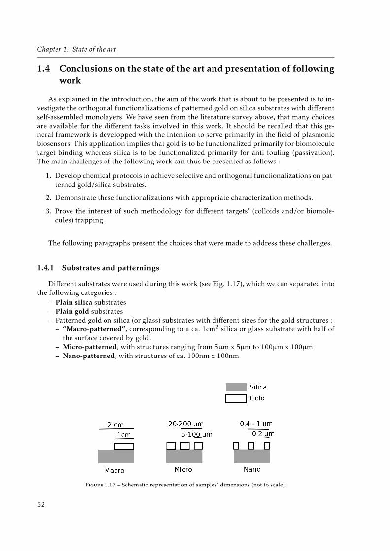
Chapter 1. State of the art
1.4 Conclusions on the state of the art and presentation of followingwork
As explained in the introduction, the aim of the work that is about to be presented is to in-vestigate the orthogonal functionalizations of patterned gold on silica substrates with differentself-assembled monolayers. We have seen from the literature survey above, that many choicesare available for the different tasks involved in this work. It should be recalled that this ge-neral framework is developped with the intention to serve primarily in the field of plasmonicbiosensors. This application implies that gold is to be functionalized primarily for biomoleculetarget binding whereas silica is to be functionalized primarily for anti-fouling (passivation).The main challenges of the following work can thus be presented as follows :
1. Develop chemical protocols to achieve selective and orthogonal functionalizations on pat-terned gold/silica substrates.
2. Demonstrate these functionalizations with appropriate characterization methods.
3. Prove the interest of such methodology for different targets’ (colloids and/or biomole-cules) trapping.
The following paragraphs present the choices that were made to address these challenges.
1.4.1 Substrates and patternings
Different substrates were used during this work (see Fig. 1.17), which we can separated intothe following categories :
– Plain silica substrates– Plain gold substrates– Patterned gold on silica (or glass) substrates with different sizes for the gold structures :
– “Macro-patterned”, corresponding to a ca. 1cm2 silica or glass substrate with half ofthe surface covered by gold.
– Micro-patterned, with structures ranging from 5µm x 5µm to 100µm x 100µm– Nano-patterned, with structures of ca. 100nm x 100nm
Figure 1.17 – Schematic representation of samples’ dimensions (not to scale).
52
1.4. Conclusions on the state of the art and presentation of following work
The reasons for working with all these different substrates can be summarized as follows :Plain substrates are the easiest to obtain and allow an easy monitoring of different functionali-zations by methods such as PM-IRRAS, XPS or contact angle goniometry. They were thereforeused for investigating and optimizing different protocols independent of orthogonal functio-nalizations (eg : NHS activation of COOH-terminated SAMs). Nano-patterned substrates arethe most promising in terms of applications, namely in the field of biophotonic transducers.However given the difficulty of characterizing surface chemistry at that scale and the fact thattheir fabrication remains rather time-consuming, it was decided to test orthogonal functiona-lizations on macro and micro-patterned substrates as well.
Plain substrates were either commercial (silica on silicon wafer and glass slides) or madeby deposition (e-beam evaporation for gold or sputtering for silica) of a thin film on a sili-con wafer (macro-patterned substrates were made by masking half of the substrate duringgold evaporation). Micro-patterned substrates were made by Ultraviolet (UV)-lithography andnano-patterned ones by e-beam lithography. These substrates were prepared either by myselfor by co-workers, as explained in appendix A.
1.4.2 Functionalizations and applications
Two main molecules were used for gold functionalization : MUA with subsequent NHSactivation and MU-Biot. These choices were made for their ability to bind amine-containingmolecules (such as proteins) and avidins (neutravidin, streptavidin) respectively. Also, thesethiols are long enough to ensure, in principle, well-ordered SAMs and are readily availablecommercially. Both thiols were used in pure SAM as well as in combination with 11-mercapto-1-undecanol to form mixed-SAMs, though no significant improvement was noticed in such bi-nary SAMs. Other thiols investigated in collaboration with the work of Alice Goudot and AnaïsGarnier include COOH and CH3 terminated PEG-thiols (HS-(CH2)10-EG3,6-COOH and HS-(CH2)10-EG3,6-CH3). Eventually perfluorinated thiols (1H,1H,2H,2H-Perfluorodecanethiol)were also used, mainly for ToF-SIMS and XPS imaging.
On silica PEG-Si was used for passivation, as well as SiF mainly for ToF-SIMS and XPSelement imaging.
Details on the functionalization and activation protocols are given in the next chapter.These functionalizations were tested in regards of two different applications :
1. The localized positioning of colloidal carboxylatex from solution onto previously definedregions of a heterogenous substrate.
2. The selective binding of target biomolecules onto LSPR-supporting nanostructures.
1.4.3 Characterizations
In the course of this PhD, the following characterization methods were used :
– For substrate characterization (prior to functionalization) :– SEM, to ensure the presence and conformity of the patterns.– PM-IRRAS and XPS to check the cleanliness and oxidation of the surface.– AFM and XRD for information on roughness and crystallinity.
– For chemical characterization of SAMs– PM-IRRAS on bare gold and “macro-patterned” surfaces.
53

Chapter 1. State of the art
– XPS on bare gold, silica and “macro-patterned” surfaces, as well as micropatterned(element imaging).
– Contact angle goniometry on bare gold, silica and “macro-patterned” surfaces.– AFM on bare gold surfaces.– ToF-SIMS on bare gold and micropatterned surfaces (element imaging).
– For evaluation of the target-binding applications– SEM to visualize the position of deposited nano-objects.– SPR or LSPR for monitoring target biomolecule binding.
54
References
[1] D.-J. Kim and K.-K. Koo. J. Ind. Eng. Chem., 10,920–926 (2004).
[2] J. Lahiri, L. Isaacs, J. Tien, and G. M. Whitesides. Analytical chemistry, 71,777–90 (1999).
[3] J. Lahiri, L. Isaacs, B. Grzybowski, J. D. Carbeck, and G. M. Whitesides. Langmuir,15,7186–7198 (1999).
[4] J. Lahiri, E. Ostuni, and G. M. Whitesides. Langmuir, 15,2055–2060 (1999).
[5] A. Myrskog, H. Anderson, T. Aastrup, B. Ingemarsson, and B. Liedberg. Langmuir,26,821–9 (2010).
[6] A. R. Lokanathan, S. Zhang, V. R. Regina, M. a. Cole, R. Ogaki, M. Dong, F. Besenbacher,R. L. Meyer, and P. Kingshott. Biointerphases, 6,180–8 (2011).
[7] S. R. Coyer, E. Delamarche, and A. J. García. Advanced materials, 23,1550–1553 (2011).
[8] C. a. Simpson, A. C. Agrawal, A. Balinski, K. M. Harkness, and D. E. Cliffel. ACS nano,5,3577–84 (2011).
[9] M. Bruns, C. Barth, P. Brüner, S. Engin, T. Grehl, C. Howell, P. Koelsch, P. Mack, P. Na-gel, V. Trouillet, D. Wedlich, and R. G. White. Surface and Interface Analysis, 44,909–913 (2012).
[10] V. Sanz, J. a. Conde, Y. Hernández, P. V. Baptista, M. R. Ibarra, and J. M. Fuente. Journalof Nanoparticle Research, 14,917 (2012).
[11] M. J. Shuster, A. Vaish, M. L. Gilbert, M. Martinez-Rivera, R. M. Nezarati, P. S. Weiss, andA. M. Andrews. The Journal of Physical Chemistry C, 115,24778–24787 (2011).
[12] K. L. Prime and G. M. Whitesides. Science, 245,1164–1167 (1991).
[13] K. L. Prime and G. M. Whitesides. Journal of the American Chemical Society, 115,10714–10721 (1993).
[14] M. Mrksich and G. M. Withesides. Annu. Rev. Biophys. Biomol. Struct., 25,55–78 (1996).
[15] G. B. Sigal, C. Bamdad, A. Barberis, J. Strominger, and G. M. Whitesides. Anal. Chem.,68,490–497 (1996).
[16] B. T. Houseman and M. Mrksich. Biomaterials, 22,943–55 (2001).
[17] B. T. Houseman, J. H. Huh, S. J. Kron, and M. Mrksich. Nature biotechnology, 20,270–274 (2002).
[18] B. T. Houseman, E. S. Gawalt, and M. Mrksich. Langmuir, 19,1522–1531 (2003).
[19] L. Li, S. Chen, J. Zheng, B. D. Ratner, and S. Jiang. The Journal of Physical Chemistry B,109,2934–41 (2005).
[20] Q. Yu, S. Chen, A. D. Taylor, J. Homola, B. Hock, and S. Jiang. Sensors and Actuators B,107,193–201 (2005).
55

References
[21] R. Valiokas, L. Malysheva, A. Onipko, H.-H. Lee, v. Ružele, S. Svedhem, S. C. T. Svensson,U. Gelius, and B. Liedberg. Journal of Electron Spectroscopy and Related Phenomena, 172,9–20 (2009).
[22] J. Maciel, M. I. Oliveira, R. M. Gonçalves, and M. a. Barbosa. Acta biomaterialia, 8,3669–77 (2012).
[23] R. J. Chen, H. C. Choi, S. Bangsaruntip, E. Yenilmez, X. Tang, Q. Wang, Y.-L. Chang, andH. Dai. Journal of the American Chemical Society, 126,1563–1568 (2004).
[24] M. L. Walker, D. J. Vanderah, and K. a. Rubinson. Colloids and surfaces. B, Biointerfaces,82,450–455 (2011).
[25] S. Zorn, U. Dettinger, M. W. Skoda, R. M. Jacobs, H. Peisert, A. Gerlach, T. Chassé, andF. Schreiber. Applied Surface Science, 258,7882–7888 (2012).
[26] C. Pale-Grosdemange, E. S. Simon, K. L. Prime, and G. M. Whitesides. Journal of theAmerican Chemical Society, 113,12–20 (1991).
[27] C. H. Lalander, Y. Zheng, S. Dhuey, and S. Cabrini. ACS nano, 4,6153–6161 (2010).
[28] L. Feuz, P. Jönsson, M. P. Jonsson, and F. Höök. ACS nano, 4,2167–77 (2010).
[29] K. Kumar, A. B. Dahlin, T. Sannomiya, S. Kaufmann, L. Isa, and E. Reimhult. Nano letters,13,6122–6129 (2013).
[30] F. Palazon, V. Monnier, Y. Chevolot, J.-P. Cloarec, and E. Souteyrand. Journal of ColloidScience and Biotechnology, 2,1–14 (2013).
[31] T. Muller, A. Gerardino, T. Schnelle, S. G. Shirley, F. Bordoni, G. D. Gasperis, R. Leoni,and G. Fuhr. Journal of Physics D : Applied Physics, 29,340–349 (1996).
[32] J. Shi, S. S. Guo, M. H. Sun, D. Baigl, and Y. Chen. Microelectronic Engineering, 84,1471–1475 (2007).
[33] Y. Yin, Y. Lu, B. Gates, and Y. Xia. Journal of the American Chemical Society, 123,8718–29 (2001).
[34] X. D. Hoa, M. Martin, a. Jimenez, J. Beauvais, P. Charette, a. Kirk, and M. Tabrizian.Biosensors & bioelectronics, 24,976–81 (2008).
[35] Q. Zhang, T. Xu, D. Butterfield, M. J. Misner, D. Y. Ryu, T. Emrick, and T. P. Russell. Nanoletters, 5,357–61 (2005).
[36] D. Baranov, A. Fiore, M. van Huis, C. Giannini, A. Falqui, U. Lafont, H. Zandbergen,M. Zanella, R. Cingolani, and L. Manna. Nano letters, 10,743–749 (2010).
[37] P. J. Pauzauskie, A. Radenovic, E. Trepagnier, H. Shroff, P. Yang, and J. Liphardt. Naturematerials, 5,97–101 (2006).
[38] R. Krupke, F. Hennrich, H. V. Löhneysen, and M. M. Kappes. Science (New York, N.Y.),301,344–7 (2003).
[39] N. Sui, V. Monnier, Y. Zakharko, Y. Chevolot, S. Alekseev, J.-M. Bluet, V. Lysenko, andE. Souteyrand. Journal of Nanoparticle Research, 14 (2012).
[40] R. M. Erb, H. S. Son, B. Samanta, V. M. Rotello, and B. B. Yellen. Nature, 457,999–1002 (2009).
[41] J. Choma, D. Jamioła, J. Ludwinowicz, and M. Jaroniec. Colloids and Surfaces A : Physico-chemical and Engineering Aspects, 411,74–79 (2012).
[42] J. Yuan, Y. Xu, A. Walther, S. Bolisetty, M. Schumacher, H. Schmalz, M. Ballauff, andA. H. E. Müller. Nature materials, 7,718–722 (2008).
56
[43] D. Cheon, S. Kumar, and G.-H. Kim. Applied Physics Letters, 96,013101 (2010).
[44] W. Ahmed, E. S. Kooij, A. van Silfhout, and B. Poelsema. Nano letters, 9,3786–94 (2009).
[45] P. a. Smith, C. D. Nordquist, T. N. Jackson, T. S. Mayer, B. R. Martin, J. Mbindyo, and T. E.Mallouk. Applied Physics Letters, 77,1399 (2000).
[46] Y. Xia, Y. Yin, Y. Lu, and J. McLellan. Advanced Functional Materials, 13,907–918 (2003).
[47] M. Rycenga, P. H. C. Camargo, and Y. Xia. Soft Matter, 5,1129 (2009).
[48] D. Xia, a. Biswas, D. Li, and S. R. J. Brueck. Advanced Materials, 16,1427–1432 (2004).
[49] D. Xia and S. R. J. Brueck. Journal of Vacuum Science & Technology B : Microelectronics andNanometer Structures, 22,3415 (2004).
[50] B. J. P. Spatz, F.-m. Kamm, A. Plettl, and P. Ziemann. Advanced Materials, 14,1827–1832 (2002).
[51] J. Huang, R. Fan, S. Connor, and P. Yang. Angewandte Chemie (International ed. in English),46,2414–7 (2007).
[52] L. Malaquin, T. Kraus, H. Schmid, E. Delamarche, and H. Wolf. Langmuir, 23,11513–21 (2007).
[53] A. Cerf, C. Thibault, M. Geneviève, and C. Vieu. Microelectronic Engineering, 86,1419–1423 (2009).
[54] A. Cerf, G. Molnár, and C. Vieu. ACS applied materials & interfaces, 1,2544–50 (2009).
[55] A. Cerf and C. Vieu. Colloids and Surfaces A : Physicochemical and Engineering Aspects,342,136–140 (2009).
[56] C. Hamon, M. Postic, E. Mazari, T. Bizien, C. Dupuis, P. Even-Hernandez, A. Jimenez,L. Courbin, C. Gosse, F. Artzner, and V. Marchi-Artzner. ACS nano, 6,4137–46 (2012).
[57] K. a. Arpin, J. H. Pikul, W. P. King, H. Fan, and P. V. Braun. Soft Matter, 7,10252 (2011).
[58] A. V. Blaaderen, R. Ruel, and P. Wiltzius. Nature, 385,321–323 (1997).
[59] M. J. Gordon and D. Peyrade. Applied Physics Letters, 89,053112 (2006).
[60] Y. Cui, M. T. Bjork, J. A. Liddle, C. Sonnichsen, B. Boussert, and A. P. Alivisatos. NanoLetters, 4,1093–1098 (2004).
[61] Y. Huang, X. Duan, Q. Wei, and C. M. Lieber. Science (New York, N.Y.), 291,630–3 (2001).
[62] Y. Huang, X. Duan, Y. Cui, L. J. Lauhon, K. H. Kim, and C. M. Lieber. Science, 294,1313–7 (2001).
[63] D. Whang, S. Jin, and Y. Wu. Nano Letters, 3,1255–1259 (2003).
[64] J. Y. Cheng, C. a. Ross, H. I. Smith, and E. L. Thomas. Advanced Materials, 18,2505–2521 (2006).
[65] T. P. Rivera. Assemblage convectif de colloides par forces de capillarité en milieu confiné :applications en plasmonique. PhD thesis (2009).
[66] A. Cerf. Assemblage dirigé de nano-objets. PhD thesis (2010).
[67] O. D. Velev and S. Gupta. Advanced Materials, 21,1897–1905 (2009).
[68] X. Ye and L. Qi. Nano Today, 6,608–631 (2011).
[69] O. D. Velev and K. H. Bhatt. Soft Matter, 2,738 (2006).
[70] W. Zhang, L. Huang, C. Santschi, and O. J. F. Martin. Nano letters, 10,1006–1011 (2010).
57

References
[71] R. Pethig and G. H. Markx. Trends in biotechnology, 15,426–32 (1997).
[72] A. Kuzyk. Electrophoresis, 32,2307–2313 (2011).
[73] B. Cetin and D. Li. Electrophoresis, 32,2410–27 (2011).
[74] P. J. Burke. Encyclopedia of Nanoscience and Nanotechnology, X,1–19 (2003).
[75] M. Giersig and P. Mulvaney. Langmuir, 9,3408–3413 (1993).
[76] M. Giersig and P. Mulvaney. The Journal of Physical Chemistry, 97,6334–6336 (1993).
[77] M. Bohmer. Langmuir, 12,5747–5750 (1996).
[78] M. Trau, D. A. Saville, and I. A. Aksay. Science, 272,706–709 (1996).
[79] M. Trau, D. A. Saville, and I. A. Aksay. Langmuir, 13,6375–6381 (1997).
[80] D. a. Dehlinger, B. D. Sullivan, S. Esener, and M. J. Heller. Small (Weinheim an der Berg-strasse, Germany), 3,1237–44 (2007).
[81] J. Ryu, D. Dehlinger, M. Heller, and T. Hahn. Particle & Particle Systems Characterization,26,275–282 (2009).
[82] F. Wakaya, T. Nagai, and K. Gamo. Microelectronic Engineering, 63,27–31 (2002).
[83] X. Q. Chen, T. Saito, H. Yamada, and K. Matsushige. Applied Physics Letters,78,3714 (2001).
[84] K. Yamamoto, S. Akita, and Y. Nakayama. Journal of Physics D : Applied Physics, 31,34–36 (1998).
[85] N. G. Green and H. Morgan. Journal of Physics D : Applied Physics, 30,2626–2633 (1997).
[86] N. Green and H. Morgan. Journal of Physics D : Applied Physics, 30,41–44 (1997).
[87] M. P. Hughes. Journal of colloid and interface science, 250,291–4 (2002).
[88] H. a. Pohl. Journal of Applied Physics, 22,869 (1951).
[89] H. A. Pohl. Journal of Applied Physics, 29,1182 (1958).
[90] H. A. Pohl, K. Pollock, and J. S. Crane. J. Biol. Phys., 6,133–160 (1978).
[91] T. Schnelle, R. Hagedorn, G. Fuhr, S. Fiedler, and T. Müller. Biochimica et biophysica acta,1157,127–40 (1993).
[92] T. Müller, a. M. Gerardino, T. Schnelle, S. G. Shirley, G. Fuhr, G. Gasperis, R. Leoni, andF. Bordoni. Il Nuovo Cimento D, 17,425–432 (1995).
[93] N. G. Green, H. Morgan, and J. J. Milner. Journal of biochemical and biophysical methods,35,89–102 (1997).
[94] M. P. Hughes and H. Morgan. Analytical Chemistry, 71,3441–3445 (1999).
[95] M. Hughes, H. Morgan, and M. Flynn. Journal of colloid and interface science, 220,454–457 (1999).
[96] M. P. Hughes and H. Morgan. Journal of Physics D : Applied Physics, 31,2205–2210 (1998).
[97] A. Ramos, H. Morgan, and N. G. Green. Journal of Physics D : Applied Physics, 31,2338–2353 (1998).
[98] N. Green and H. Morgan. Journal of Physics D : Applied Physics, 31,25–30 (1998).
[99] A. Ramos, H. Morgan, N. G. Green, and A. Castellanos. Journal of colloid and interfacescience, 217,420–422 (1999).
58
[100] A. Ramos, H. Morgan, N. G. Green, and A. Castellanos. Journal of electrostatics, 47,71–81 (1999).
[101] S. Fiedler, S. G. Shirley, T. Schnelle, and G. Fuhr. Analytical chemistry, 70,1909–15 (1998).
[102] T. Muller, G. Gradl, S. Howitz, S. Shirley, and G. Fuhr. Biosensors & Bioelectronics, 14,247–256 (1999).
[103] T. Schnelle, T. Müller, R. Hagedorn, a. Voigt, and G. Fuhr. Biochimica et biophysica acta,1428,99–105 (1999).
[104] L. Zheng, J. P. Brody, and P. J. Burke. Biosensors & bioelectronics, 20,606–19 (2004).
[105] N. Gadish and J. Voldman. Analytical chemistry, 78,7870–6 (2006).
[106] M. Wiklund, P. Spégel, S. Nilsson, and H. M. Hertz. Ultrasonics, 41,329–333 (2003).
[107] J. L. Baylon-Cardiel, N. M. Jesús-Pérez, A. V. Chávez-Santoscoy, and B. H. Lapizco-Encinas. Lab on a chip, 10,3235–42 (2010).
[108] E. B. Cummings and A. K. Singh. Analytical chemistry, 75,4724–31 (2003).
[109] K. Khoshmanesh, C. Zhang, F. J. Tovar-Lopez, S. Nahavandi, S. Baratchi, K. Kalantar-zadeh, and A. Mitchell. Electrophoresis, 30,3707–17 (2009).
[110] D. J. Bakewell and H. Morgan. Measurement Science and Technology, 15,254–266 (2004).
[111] D. J. Bennett, B. Khusid, C. D. James, P. C. Galambos, M. Okandan, D. Jacqmin, andA. Acrivos. Applied Physics Letters, 83,4866 (2003).
[112] A. P. Hsiao and M. J. Heller. Journal of Biomedicine and Biotechnology, 2012,1–9 (2012).
[113] R. Krishnan, D. a. Dehlinger, G. J. Gemmen, R. L. Mifflin, S. C. Esener, and M. J. Heller.Electrochemistry communications, 11,1661–1666 (2009).
[114] W. J. Tian, J. P. Huang, and K. W. Yu. Journal of Applied Physics, 105,102044 (2009).
[115] A. Rosenthal and J. Voldman. Biophysical journal, 88,2193–205 (2005).
[116] H. Zhou, L. R. White, and R. D. Tilton. Journal of colloid and interface science, 285,179–91 (2005).
[117] Z. Gagnon and H.-C. Chang. Electrophoresis, 26,3725–37 (2005).
[118] J. Wu, Y. Ben, D. Battigelli, and H.-C. Chang. Industrial & Engineering Chemistry Research,44,2815–2822 (2005).
[119] D. R. Albrecht, R. L. Sah, and S. N. Bhatia. Biophysical journal, 87,2131–2147 (2004).
[120] S. O. Lumsdon, E. W. Kaler, and O. D. Velev. Langmuir, 20,2108–2116 (2004).
[121] L. Zheng, S. Li, J. P. Brody, and P. J. Burke. Langmuir, 20,8612–9 (2004).
[122] P. K. Wong, C.-Y. Chen, T.-H. Wang, and C.-M. Ho. Analytical chemistry, 76,6908–14 (2004).
[123] J. Voldman, M. Toner, M. Gray, and M. Schmidt. Journal of Electrostatics, 57,69–90 (2003).
[124] G. Medoro, N. Manaresi, a. Leonardi, L. Altomare, M. Tartagni, and R. Guerrieri. IEEESensors Journal, 3,317–325 (2003).
[125] M. Frénéa, S. P. Faure, B. Le Pioufle, P. Coquet, and H. Fujita. Materials Science andEngineering : C, 23,597–603 (2003).
59
References
[126] K. F. Hoettges, M. B. McDonnell, and M. P. Hughes. Journal of Physics D : Applied Physics,36,101–104 (2003).
[127] J. Auerswald and H. F. Knapp. Microelectronic Engineering, 68,879–886 (2003).
[128] A. Castellanos, A. Ramos, A. Gonzalez, N. G. Green, and H. Morgan. Journal of PhysicsD : Applied Physics, 36,2584–2597 (2003).
[129] M. Dürr, J. Kentsch, T. Müller, T. Schnelle, and M. Stelzle. Electrophoresis, 24,722–31 (2003).
[130] A. Bezryadin, C. Dekker, and G. Schmid. Applied Physics Letters, 71,1273 (1997).
[131] A. Bezryadin. Journal of Vacuum Science & Technology B : Microelectronics and NanometerStructures, 15,793 (1997).
[132] B. C. Gierhart, D. G. Howitt, S. J. Chen, R. L. Smith, and S. D. Collins. Langmuir,23,12450–12456 (2007).
[133] R. Krahne, A. Yacoby, H. Shtrikman, I. Bar-Joseph, T. Dadosh, and J. Sperling. AppliedPhysics Letters, 81,730 (2002).
[134] R. Krahne, T. Dadosh, Y. Gordin, A. Yacoby, H. Shtrikman, D. Mahalu, J. Sperling,and I. Bar-Joseph. Physica E : Low-dimensional Systems and Nanostructures, 17,498–502 (2003).
[135] I. Amlani, A. M. Rawlett, L. a. Nagahara, and R. K. Tsui. Applied Physics Letters,80,2761 (2002).
[136] I. Amlani, A. M. Rawlett, L. a. Nagahara, and R. K. Tsui. Journal of Vacuum Science &Technology B : Microelectronics and Nanometer Structures, 20,2802 (2002).
[137] A. M. Rawlett, T. J. Hopson, I. Amlani, R. Zhang, J. Tresek, L. A. Nagahara, R. K. Tsui,and H. Goronkin. Nanotechnology, 14,377–384 (2003).
[138] R. J. Barsotti, M. D. Vahey, R. Wartena, Y.-M. Chiang, J. Voldman, and F. Stellacci. Small(Weinheim an der Bergstrasse, Germany), 3,488–499 (2007).
[139] S. Kumar, S.-H. Yoon, and G.-H. Kim. Current Applied Physics, 9,101–103 (2009).
[140] S. I. Khondaker and Z. Yao. Applied Physics Letters, 81,4613 (2002).
[141] T. Dadosh, Y. Gordin, R. Krahne, I. Khivrich, D. Mahalu, V. Frydman, J. Sperling, A. Ya-coby, and I. Bar-Joseph. Nature, 436,677–80 (2005).
[142] J.-S. Na, J. Ayres, K. L. Chandra, C. Chu, C. B. Gorman, and G. N. Parsons. Nanotechno-logy, 18,035203 (2007).
[143] D. L. Fan, R. C. Cammarata, and C. L. Chien. Applied Physics Letters, 92,93115 (2008).
[144] R. J. Hamers, J. D. Beck, M. a. Eriksson, B. Li, M. S. Marcus, L. Shang, J. Simmons, andJ. a. Streifer. Nanotechnology, 17,S280–S286 (2006).
[145] J. J. Boote and S. D. Evans. Nanotechnology, 16,1500–1505 (2005).
[146] H. W. Seo, C.-S. Han, S. O. Hwang, and J. Park. Nanotechnology, 17,3388–93 (2006).
[147] L. Dong, J. Bush, V. Chirayos, R. Solanki, J. Jiao, Y. Ono, J. F. Conley, and B. D. Ulrich.Nano letters, 5,2112–2115 (2005).
[148] S. Evoy, N. DiLello, V. Deshpande, a. Narayanan, H. Liu, M. Riegelman, B. R. Martin,B. Hailer, J.-C. Bradley, W. Weiss, T. S. Mayer, Y. Gogotsi, H. H. Bau, T. E. Mallouk, andS. Raman. Microelectronic Engineering, 75,31–42 (2004).
60
[149] M. Li, R. B. Bhiladvala, T. J. Morrow, J. a. Sioss, K.-K. Lew, J. M. Redwing, C. D. Keating,and T. S. Mayer. Nature nanotechnology, 3,88–92 (2008).
[150] A. D. Wissner-Gross. Nanotechnology, 17,4986–4990 (2006).
[151] E. M. Freer, O. Grachev, X. Duan, S. Martin, and D. P. Stumbo. Nature nanotechnology,5,525–30 (2010).
[152] C. S. Lao, J. Liu, P. Gao, L. Zhang, D. Davidovic, R. Tummala, and Z. L. Wang. Nanoletters, 6,263–266 (2006).
[153] S.-Y. Lee, A. Umar, D.-I. Suh, J.-E. Park, Y.-B. Hahn, J.-Y. Ahn, and S.-K. Lee. Physica E :Low-dimensional Systems and Nanostructures, 40,866–872 (2008).
[154] W. J. Liu, J. Zhang, L. J. Wan, K. W. Jiang, B. R. Tao, H. L. Li, W. L. Gong, and X. D. Tang.Sensors and Actuators B : Chemical, 133,664–670 (2008).
[155] J. Suehiro, N. Nakagawa, S.-I. Hidaka, M. Ueda, K. Imasaka, M. Higashihata, T. Okada,and M. Hara. Nanotechnology, 17,2567–73 (2006).
[156] J. Suehiro. Biomicrofluidics, 4,1–10 (2010).
[157] S. Kumar, Y.-K. Seo, and G.-H. Kim. Applied Physics Letters, 94,153104 (2009).
[158] D. Wang, R. Zhu, Z. Zhou, and X. Ye. Applied Physics Letters, 90,103110 (2007).
[159] S. Kumar, S. Rajaraman, R. a. Gerhardt, Z. L. Wang, and P. J. Hesketh. ElectrochimicaActa, 51,943–951 (2005).
[160] S.-Y. S.-K. Lee, T.-H. Kim, D.-I. Suh, E.-K. Suh, N.-K. Cho, and W.-K. Seong. AppliedPhysics A, 87,739–742 (2007).
[161] S.-K. Lee, T.-H. Kim, S.-Y. Lee, K.-C. Choi, and P. Yang. Philosophical Magazine, 87,2105–2115 (2007).
[162] A. I. Baca, J. J. Brown, K. a. Bertness, and V. M. Bright. Nanotechnology,23,245301 (2012).
[163] A. Motayed, M. He, A. V. Davydov, J. Melngailis, and S. N. Mohammad. Journal of AppliedPhysics, 100,114310 (2006).
[164] S.-Y. Lee, T.-H. Kim, D.-I. Suh, N.-K. Cho, H.-K. Seong, S.-W. Jung, H.-J. Choi, and S.-K.Lee. Chemical Physics Letters, 427,107–112 (2006).
[165] T. H. Kim, S. Y. K. Lee, N. K. Cho, H. K. Seong, H. J. Choi, and S. W. Jung. Nanotechnology,17,3394–3399 (2006).
[166] J.-W. Lee, K.-J. Moon, M.-H. Ham, and J.-M. Myoung. Solid State Communications,148,194–198 (2008).
[167] S. Raychaudhuri, S. a. Dayeh, D. Wang, and E. T. Yu. Nano letters, 9,2260–6 (2009).
[168] K. Oh, J.-H. Chung, J. J. Riley, Y. Liu, and W. K. Liu. Langmuir, 23,11932–40 (2007).
[169] T. J. Morrow, M. Li, J. Kim, T. S. Mayer, and C. D. Keating. Science, 323,2009 (2009).
[170] A. Bezryadin, R. M. Westervelt, and M. Tinkham. Applied Physics Letters, 74,2699 (1999).
[171] L. a. Nagahara, I. Amlani, J. Lewenstein, and R. K. Tsui. Applied Physics Letters,80,3826 (2002).
[172] J. Suehiro, G. Zhou, and M. Hara. Journal of Physics D : Applied Physics, 36 (2003).
[173] R. Krupke, F. Hennrich, H. B. Weber, M. M. Kappes, and H. v. Löhneysen. Nano Letters,3,1019–1023 (2003).
61
References
[174] J. Chung and J. Lee. Sensors and Actuators A : Physical, 104,229–235 (2003).
[175] J. Chung, K.-H. Lee, J. Lee, and R. S. Ruoff. Langmuir, 20,3011–7 (2004).
[176] C. K. M. Fung, V. T. S. Wong, R. H. M. Chan, and W. J. Li. IEEE Transactions On Nano-technology, 3,395–403 (2004).
[177] J. Suehiro, G. Zhou, H. Imakiire, W. Ding, and M. Hara. Sensors and Actuators B : Chemi-cal, 108,398–403 (2005).
[178] H.-W. Seo, C.-S. Han, D.-G. Choi, K.-S. Kim, and Y.-H. Lee. Microelectronic Engineering,81,83–89 (2005).
[179] M. Lucci, P. Regoliosi, a. Reale, a. Di Carlo, S. Orlanducci, E. Tamburri, M. L. Terranova,P. Lugli, C. Di Natale, a. D’Amico, and R. Paolesse. Sensors and Actuators B : Chemical,111-112,181–186 (2005).
[180] R. Krupke, S. Linden, M. Rapp, and F. Hennrich. Advanced Materials, 18,1468–1470 (2006).
[181] M. Lucci, a. Reale, a. Di Carlo, S. Orlanducci, E. Tamburri, M. L. Terranova, I. Davoli,C. Di Natale, a. D’Amico, and R. Paolesse. Sensors and Actuators B : Chemical, 118,226–231 (2006).
[182] M. Dimaki and P. Bø ggild. Physica Status Solidi (a), 203,1088–1093 (2006).
[183] J.-E. Kim, J.-K. Park, and C.-S. Han. Nanotechnology, 17,2937–2941 (2006).
[184] D. Sickert, S. Taeger, I. Kühne, M. Mertig, W. Pompe, and G. Eckstein. Physica StatusSolidi (B), 243,3542–3545 (2006).
[185] M. Riegelman, H. Liu, and H. H. Bau. Journal of Fluids Engineering, 128,6 (2006).
[186] R. Zhou, P. Wang, and H.-C. Chang. Electrophoresis, 27,1376–85 (2006).
[187] K. Wai, C. Lai, C. Kar, M. Fung, V. Tak, S. Wong, M. Lai, Y. Sin, W. J. Li, and C.-p. Kwong.IEEE Transactions on automation science and engineering, 3,218–227 (2006).
[188] Z.-B. Zhang, S.-L. Zhang, and E. E. B. Campbell. Chemical Physics Letters, 421,11–15 (2006).
[189] S. Taeger, D. Sickert, P. Atanasov, G. Eckstein, and M. Mertig. Physica Status Solidi (B),243,3355–3358 (2006).
[190] N. Mureau, E. Mendoza, and S. R. P. Silva. Electrophoresis, 28,1495–8 (2007).
[191] T. Schwamb, T.-Y. Choi, N. Schirmer, N. R. Bieri, B. Burg, J. Tharian, U. Sennhauser, andD. Poulikakos. Nano Letters, 7,3633–3638 (2007).
[192] A. Vijayaraghavan, S. Blatt, D. Weissenberger, M. Oron-Carl, F. Hennrich, D. Gerthsen,H. Hahn, and R. Krupke. Nano letters, 7,1556–1560 (2007).
[193] J. Suehiro, N. Ikeda, A. Ohtsubo, and K. Imasaka. Microfluidics and Nanofluidics, 5,741–747 (2008).
[194] S. Rao, L. Huang, and W. Setyawan. Nature, 425,36–37 (2003).
[195] L. Huang, Z. Jia, and S. O’Brien. Journal of Materials Chemistry, 17,3863 (2007).
[196] A. Ashkin and J. M. Dziedzic. Applied Physics Letters, 19,283 (1971).
[197] A. Ashkin and J. M. Dziedzic. Applied Physics Letters, 30,202 (1977).
[198] A. Ashkin, J. M. Dziedzic, J. E. Bjorkholm, and S. Chu. Optics letters, 11,816–818 (1986).
[199] A. Ashkin. Selected Topics in Quantum Electronics, IEEE, 6,841–856 (2000).
62
[200] D. G. Grier. Nature, 424,810–6 (2003).
[201] K. C. Neuman and S. M. Block. The Review of scientific instruments, 75,2787–2809 (2004).
[202] K. Dholakia and P. Reece. Nano Today, 1,18–27 (2006).
[203] K. Dholakia, P. Reece, and M. Gu. Chemical Society reviews, 37,42–55 (2008).
[204] K. C. Neuman and A. Nagy. Nature methods, 5,491–505 (2008).
[205] J. R. Moffitt, Y. R. Chemla, S. B. Smith, and C. Bustamante. Annual review of biochemistry,77,205–228 (2008).
[206] S. Kinge, M. Crego-Calama, and D. N. Reinhoudt. Chemphyschem : a European journal ofchemical physics and physical chemistry, 9,20–42 (2008).
[207] J. Homola and J. Dostálek. Surface plasmon resonance based sensors (2006).
[208] M. L. Juan, M. Righini, and R. Quidant. Nature Photonics, 5,349–356 (2011).
[209] S. Kawata and T. Tani. Optics letters, 21,1768–70 (1996).
[210] L. Novotny, R. Bian, and X. Xie. Physical Review Letters, 79,645–648 (1997).
[211] P. Chaumet, A. Rahmani, and M. N. Vesperinas. Physical Review Letters, 88,10–13 (2002).
[212] M. N. Vesperinas, P. C. Chaumet, and A. Rahmani. Philosophical transactions. Series A,Mathematical, physical, and engineering sciences, 362,719–37 (2004).
[213] K. Okamoto and S. Kawata. Physical review letters, 83,4534–4537 (1999).
[214] E. Kwak, T. Onuta, and D. Amarie. J. Phys. Chem. B, 108,13607–13612 (2004).
[215] R. Quidant, D. Petrov, and G. Badenes. Optics letters, 30,1009–11 (2005).
[216] M. Righini, A. S. Zelenina, C. Girard, and R. Quidant. Nature Physics, 3,477–480 (2007).
[217] M. Righini, P. Ghenuche, S. Cherukulappurath, V. Myroshnychenko, F. García de Abajo,and R. Quidant. Nano letters, 9,3387–3391 (2009).
[218] Z. Fang, F. Lin, S. Huang, W. Song, and X. Zhu. Applied Physics Letters, 94,63306 (2009).
[219] a. N. Grigorenko, N. W. Roberts, M. R. Dickinson, and Y. Zhang. Nature Photonics, 2,365–370 (2008).
[220] A. Baev, E. P. Furlani, P. N. Prasad, A. N. Grigorenko, and N. W. Roberts. Journal ofApplied Physics, 103,084316 (2008).
[221] M. Righini, G. Volpe, C. Girard, D. Petrov, and R. Quidant. Physical Review Letters, 100,8–11 (2008).
[222] H. M. K. Wong, M. Righini, J. C. Gates, P. G. R. Smith, V. Pruneri, and R. Quidant. AppliedPhysics Letters, 99,061107 (2011).
[223] B. J. Roxworthy, K. D. Ko, A. Kumar, K. H. Fung, E. K. C. Chow, G. L. Liu, N. X. Fang,and K. C. Toussaint. Nano letters, 12,796–801 (2012).
[224] J. E. Curtis, B. A. Koss, and D. G. Grier. Optics Communications, 207,169–175 (2002).
[225] R. Agarwal, K. Ladavac, Y. Roichman, G. Yu, C. Lieber, and D. Grier. Optics express,13,8906–8912 (2005).
[226] W. Hossack, E. Theofanidou, J. Crain, K. Heggarty, and M. Birch. Optics express, 11,2053–2059 (2003).
[227] E. Schonbrun, R. Piestun, P. Jordan, J. Cooper, K. Wulff, J. Courtial, and M. Padgett.Optics express, 13,3777–3786 (2005).
63
References
[228] S. S. Guo, Y. L. Deng, L. B. Zhao, H. L. W. Chan, and X.-Z. Zhao. Journal of Physics D :Applied Physics, 41,105008 (2008).
[229] C. Mikkelsen, M. Fougt Hansen, and H. Bruus. Journal of Magnetism and Magnetic Mate-rials, 293,578–583 (2005).
[230] C. Mikkelsen and H. Bruus. Lab on a chip, 5,1293–7 (2005).
[231] E. P. Furlani. Journal of Applied Physics, 99,24912 (2006).
[232] E. Furlani and K. Ng. Physical Review E, 73,1–10 (2006).
[233] K. Smistrup, M. Bu, A. Wolff, H. Bruus, and M. F. Hansen. Microfluidics and Nanofluidics,4,565–573 (2008).
[234] B. Hallmark, N. J. Darton, T. James, P. Agrawal, and N. K. H. Slater. Journal of NanoparticleResearch, 12,2951–2965 (2010).
[235] M. Berger, J. Castelino, R. Huang, M. Shah, and R. H. Austin. Electrophoresis, 22,3883–92 (2001).
[236] I. F. Lyuksyutov, D. G. Naugle, and K. D. D. Rathnayaka. Applied Physics Letters,85,1817 (2004).
[237] Z. G. Forbes, B. B. Yellen, K. A. Barbee, and G. Friedman. IEEE Transactions on Magnetics,39,3372–3377 (2003).
[238] Y. A. Lin, T.-S. Wong, U. Bhardwaj, J.-M. Chen, E. McCabe, and C.-M. Ho. Journal ofMicromechanics and Microengineering, 17,1299–1306 (2007).
[239] T. Lund-Olesen, H. Bruus, and M. F. Hansen. Biomedical microdevices, 9,195–205 (2007).
[240] H. Chen, M. D. Kaminski, and A. J. Rosengart. Medical engineering & physics, 30,1–8 (2008).
[241] D. W. Inglis, R. Riehn, R. H. Austin, and J. C. Sturm. Applied Physics Letters,85,5093 (2004).
[242] K.-H. Han and a. B. Frazier. Journal of Micromechanical Systems, 14,67–73 (2005).
[243] K.-H. Han and a. B. Frazier. Lab on a chip, 6,265–73 (2006).
[244] J.-W. Choi, C. H. Ahn, S. Bhansali, and H. Henderson. Sensors and Actuators B : Chemical,68,34–39 (2000).
[245] J. W. Choi, T. M. Liakopoulos, and C. H. Ahn. Biosensors & bioelectronics, 16,409–416 (2001).
[246] C. H. Ahn, M. G. Allen, W. Trimmer, Y.-N. Jun, and S. Erramilli. Journal of Microelectro-mechanical Systems, 5,151–158 (1996).
[247] J. Do, J.-w. Choi, and C. H. Ahn. IEEE Transactions on Magnetics, 40,3009–3011 (2004).
[248] Q. Ramadan, V. Samper, D. Poenar, and C. Yu. Journal of Magnetism and Magnetic Mate-rials, 281,150–172 (2004).
[249] Q. Ramadan, V. Samper, D. Poenar, and C. Yu. International Journal of Nanoscience, 4,489–499 (2005).
[250] Q. Ramadan, V. Samper, D. P. Poenar, and C. Yu. Biosensors & bioelectronics, 21,1693–702 (2006).
[251] Q. Ramadan, C. Yu, V. Samper, and D. P. Poenar. Applied Physics Letters, 88,32501 (2006).
[252] Q. Ramadan, V. Samper, D. Poenar, Z. Liang, C. Yu, and T. M. Lim. Sensors and ActuatorsB : Chemical, 113,944–955 (2006).
64
[253] Q. Ramadan, D. P. Poenar, and C. Yu. Microfluidics and Nanofluidics, 6,53–62 (2008).
[254] M. Barbic, J. J. Mock, A. P. Gray, and S. Schultz. Applied Physics Letters, 79,1897 (2001).
[255] S.-H. Song, B.-S. Kwak, J.-S. Park, W. Kim, and H.-I. Jung. Sensors and Actuators A :Physical, 151,64–70 (2009).
[256] S.-H. Song, H.-L. Lee, Y. H. Min, and H.-I. Jung. Sensors and Actuators B : Chemical,141,210–216 (2009).
[257] M. Tondra, M. Granger, R. Fuerst, M. Porter, C. Nordman, J. Taylor, and S. Akou. IEEETransactions on Magnetics, 37,2621–2623 (2001).
[258] N. Pekas, M. Granger, M. Tondra, A. Popple, and M. D. Porter. Journal of Magnetism andMagnetic Materials, 293,584–588 (2005).
[259] T. Deng, G. M. Whitesides, M. Radhakrishnan, G. Zabow, and M. Prentiss. Applied PhysicsLetters, 78,1775 (2001).
[260] C. Liu, L. Lagae, R. Wirix-Speetjens, and G. Borghs. Journal of Applied Physics,101,024913 (2007).
[261] K. Smistrup, B. G. Kjeldsen, J. L. Reimers, M. Dufva, J. Petersen, and M. F. Hansen. Labon a chip, 5,1315–9 (2005).
[262] K. Smistrup, O. Hansen, H. Bruus, and M. F. Hansen. Journal of Magnetism and MagneticMaterials, 293,597–604 (2005).
[263] K. Smistrup, T. Lund-Olesen, M. F. Hansen, and P. T. Tang. Journal of Applied Physics,99,08P102 (2006).
[264] K. Smistrup, P. T. Tang, O. Hansen, and M. F. Hansen. Journal of Magnetism and MagneticMaterials, 300,418–426 (2006).
[265] N. Haddour, Y. Chevolot, M. Trévisan, E. Souteyrand, and J.-P. Cloarec. Journal of Mate-rials Chemistry, 20,8266 (2010).
[266] M. a. M. Gijs, F. Lacharme, and U. Lehmann. Chemical reviews, 110,1518–1563 (2010).
[267] A.-E. Saliba, L. Saias, E. Psychari, N. Minc, D. Simon, F.-C. Bidard, C. Mathiot, J.-Y.Pierga, V. Fraisier, J. Salamero, V. Saada, F. Farace, P. Vielh, L. Malaquin, and J.-L. Viovy.Proceedings of the National Academy of Sciences of the United States of America, 107,14524–14529 (2010).
[268] B. B. Yellen, O. Hovorka, and G. Friedman. Proceedings of the National Academy of Sciencesof the United States of America, 102,8860–8864 (2005).
[269] T. Henighan, D. Giglio, a. Chen, G. Vieira, and R. Sooryakumar. Applied Physics Letters,98,103505 (2011).
[270] T. Deng, M. Prentiss, and G. M. Whitesides. Applied Physics Letters, 80,461 (2002).
[271] B. Yellen, G. Friedman, and a. Feinerman. Journal of Applied Physics, 93,7331 (2003).
[272] S. Guo, C. Zuo, W. Huang, C. Peroz, and Y. Chen. Microelectronic Engineering, 83,1655–1659 (2006).
[273] T. Henighan, a. Chen, G. Vieira, a. J. Hauser, F. Y. Yang, J. J. Chalmers, and R. Sooryaku-mar. Biophysical journal, 98,412–7 (2010).
[274] G. Ruan, G. Vieira, T. Henighan, A. Chen, D. Thakur, R. Sooryakumar, and J. O. Winter.Nano letters, 10,2220–4 (2010).
[275] P. Tseng, D. Di Carlo, and J. W. Judy. Nano letters, 9,3053–9 (2009).
65

References
[276] Y.-J. Liu, S.-S. Guo, Z.-L. Zhang, W.-H. Huang, D. Baigl, M. Xie, Y. Chen, and D.-W. Pang.Electrophoresis, 28,4713–22 (2007).
[277] M. Liu, J. Lagdani, H. Imrane, C. Pettiford, J. Lou, S. Yoon, V. G. Harris, C. Vittoria, andN. X. Sun. Applied Physics Letters, 90,103105 (2007).
[278] Y. Rheem, C. M. Hangarter, and N. V. Myung. IEEE Transactions on Nanotechnology,7,251–255 (2008).
[279] C. M. Hangarter, Y. Rheem, B. Yoo, E.-H. Yang, and N. V. Myung. Nanotechnology,18,205305 (2007).
[280] M. Tanase, D. M. Silevitch, a. Hultgren, L. a. Bauer, P. C. Searson, G. J. Meyer, and D. H.Reich. Journal of Applied Physics, 91,8549 (2002).
[281] D. P. Long, J. L. Lazorcik, and R. Shashidhar. Advanced Materials, 16,814–819 (2004).
[282] M. Liu, X. Li, H. Imrane, Y. Chen, T. Goodrich, Z. Cai, K. S. Ziemer, J. Y. Huang, and N. X.Sun. Applied Physics Letters, 90,152501 (2007).
[283] R. J. Kershner, J. W. Bullard, and M. J. Cima. Journal of colloid and interface science,278,146–54 (2004).
[284] H. Fudouzi, M. Kobayashi, and N. Shinya. Journal of Nanoparticle Research, 3,193–200 (2001).
[285] R. M. Erb, N. J. Jenness, R. L. Clark, and B. B. Yellen. Advanced materials (Deerfield Beach,Fla.), 21,4825–9 (2009).
[286] D. Braun and A. Libchaber. Physical Review Letters, 89,2–5 (2002).
[287] R. T. Schermer, C. C. Olson, J. P. Coleman, and F. Bucholtz. Optics express, 19,10571–86 (2011).
[288] T. Lilliehorn, U. Simu, M. Nilsson, M. Almqvist, T. Stepinski, T. Laurell, J. Nilsson, andS. Johansson. Ultrasonics, 43,293–303 (2005).
[289] H. M. Hertz. Journal of Applied Physics, 78,4845 (1995).
[290] P. Glynne-Jones, C. E. M. Démoré, C. Ye, Y. Qiu, S. Cochran, and M. Hill. IEEE transac-tions on ultrasonics, ferroelectrics, and frequency control, 59,1258–66 (2012).
[291] J. Lee, C. Lee, and K. K. Shung. IEEE transactions on ultrasonics, ferroelectrics, and fre-quency control, 57,2305–10 (2010).
[292] F. Zheng, Y. Li, H.-S. Hsu, C. Liu, C. Tat Chiu, C. Lee, H. Ham Kim, and K. K. Shung.Applied Physics Letters, 101,214104 (2012).
[293] M. Kolibal, M. Konecny, F. Ligmajer, D. Skoda, T. Vystavel, J. Zlamal, P. Varga, and T. Si-kola. ACS nano, 6,10098–10106 (2012).
[294] R. Nidetz and J. Kim. Nanotechnology, 23,45602 (2012).
[295] S. Gilles, C. Kaulen, M. Pabst, U. Simon, a. Offenhäusser, and D. Mayer. Nanotechnology,22,295301 (2011).
[296] P. Maury, M. Escalante, D. N. Reinhoudt, and J. Huskens. Advanced Materials, 17,2718–2723 (2005).
[297] J. Yang, K. Im, and S. Lim. Applied Surface Science, 257,5476–5479 (2011).
[298] Y. Jie, J. R. Niskala, A. C. Johnston-Peck, P. J. Krommenhoek, J. B. Tracy, H. Fan, andW. You. Journal of Materials Chemistry, 22,1962 (2012).
66
[299] M. Trevisan, Y. Chevolot, V. Monnier, J.-P. Cloarec, E. Souteyrand, A. Duval, J. Moreau,and M. Canva. International Journal of Nanoscience, 11,1240012 (2012).
[300] Y. Zheng, C. H. Lalander, T. Thai, S. Dhuey, S. Cabrini, and U. Bach. Angewandte Chemie(International ed. in English), 50,4398–4402 (2011).
[301] M. Trévisan, M. Schawaller, G. Quapil, E. Souteyrand, Y. Mérieux, and J.-P. Cloarec. Bio-sensors & bioelectronics, 26,1631–1637 (2010).
[302] J. C. Love, L. a. Estroff, J. K. Kriebel, R. G. Nuzzo, and G. M. Whitesides. Chemical reviews,105,1103–1169 (2005).
[303] F. Schreiber. Progress in Surface Science, 65,151–256 (2000).
[304] C. Vericat, M. E. Vela, G. Benitez, P. Carro, and R. C. Salvarezza. Chemical Society reviews,39,1805–1834 (2010).
[305] R. Colorado, R. J. Villazana, and T. R. Lee. Langmuir, 14,6337–6340 (1998).
[306] Y.-s. Shon and T. R. Lee. The Journal of Physical Chemistry B, 104,8192–8200 (2000).
[307] Y.-s. Shon, S. M. Gross, B. Dawson, M. Porter, and R. W. Murray. Langmuir, 16,6555–6561 (2000).
[308] M. Lereau, C. Fournier-Wirth, J. Mayen, C. Farre, A. Meyer, V. Dugas, J.-F. Cantaloube,C. Chaix, J.-J. Vasseur, and F. Morvan. Analytical chemistry, 85,9204–12 (2013).
[309] T. R. Lee, P. Chinwangso, and A. C. Jamison. Accounts of chemical research, 44,511–519 (2011).
[310] J. M. Tour, L. Jones, D. L. Pearson, J. J. S. Lamba, T. P. Burgin, G. M. Whitesides, D. L.Allara, A. N. Parikh, and S. Atre. Journal of the American Chemical Society, 117,9529–9534 (1995).
[311] E. B. Troughton, C. D. Bain, G. M. Whitesides, R. G. Nuzzo, D. L. Allara, and M. D. Porter.Langmuir, 4,365–385 (1988).
[312] R. G. Nuzzo and D. L. Allara. Journal of the American Chemical Society, 105,4481–4483 (1983).
[313] T. M. Willey, A. L. Vance, C. Bostedt, T. van Buuren, R. W. Meulenberg, L. J. Terminello,and C. S. Fadley. Langmuir, 20,4939–44 (2004).
[314] Z. Li, T. Niu, Z. Zhang, G. Feng, and S. Bi. Thin Solid Films, 519,4225–4233 (2011).
[315] M. Suzuki, T. Miyazaki, H. Hisamitsu, Y. Kadoma, and Y. Morioka. Langmuir, 15,7409–7410 (1999).
[316] A. T. Lusk and G. K. Jennings. Langmuir, 17,7830–7836 (2001).
[317] L. V. Protsailo, W. R. Fawcett, D. Russell, and R. L. Meyer. Langmuir, 18,9342–9349 (2002).
[318] S. W. Han and K. Kim. Journal of colloid and interface science, 240,492–497 (2001).
[319] Y.-s. Shon, S. Lee, R. Colorado, S. S. Perry, and T. R. Lee. Langmuir, 122,7556–7563 (2000).
[320] F. Tielens, V. Humblot, C.-M. Pradier, M. Calatayud, and F. Illas. Langmuir, 25,9980–9985 (2009).
[321] T. Sawaguchi, Y. Sato, and F. Mizutani. Journal of Electroanalytical Chemistry, 496,50–60 (2001).
67
References
[322] H. Munakata, S. Kuwabata, Y. Ohko, and H. Yoneyama. Journal of Electroanalytical Che-mistry, 496,29–36 (2001).
[323] S.-i. Imabayashi, N. Gon, T. Sasaki, D. Hobara, and T. Kakiuchi. Langmuir, 14,2348–2351 (1998).
[324] S.-i. Imabayashi, D. Hobara, T. Kakiuchi, and W. Knoll. Langmuir, 13,4502–4504 (1997).
[325] D. Hobara, T. Sasaki, S.-i. Imabayashi, and T. Kakiuchi. Langmuir, 15,5073–5078 (1999).
[326] D. Hobara, M. Ota, S.-i. Imabayashi, K. Niki, and T. Kakiuchi. Journal of ElectroanalyticalChemistry, 444,113–119 (1998).
[327] D. Hobara and T. Kakiuchi. Electrochemistry communications, 3,154–157 (2001).
[328] C. Singh, A. M. Jackson, F. Stellacci, and S. C. Glotzer. Journal of the American ChemicalSociety, 131,16377–16379 (2009).
[329] M. L. Carot, V. Macagno, P. Paredes-Olivera, and E. M. Patrito. Journal of Physical Che-mistry C, 111,4294–4304 (2007).
[330] J. W. Lee, S. J. Sim, S. M. Cho, and J. Lee. Biosensors & bioelectronics, 20,1422–7 (2005).
[331] S. Chen, L. Li, C. L. Boozer, and S. Jiang. Langmuir, 16,9287–9293 (2000).
[332] K. Tamada, M. Hara, H. Sasabe, and W. Knoll. Langmuir, 7463,1558–1566 (1997).
[333] R. L. Grimm, N. M. Barrentine, C. J. H. Knox, and J. C. Hemminger. Journal of PhysicalChemistry C, 112,890–894 (2008).
[334] E. Briand, M. Salmain, J.-m. Herry, H. Perrot, C. Compère, and C.-m. Pradier. Biosensorsand Bioelectronics, 22,440–448 (2006).
[335] E. Briand, M. Salmain, C. Compère, and C.-M. Pradier. Biosensors & bioelectronics,22,2884–90 (2007).
[336] E. Briand, M. Salmain, C. Compère, and C.-M. Pradier. Colloids and surfaces. B, Biointer-faces, 53,215–24 (2006).
[337] J.-M. Chang, F.-G. Tseng, and C.-C. Chieng. IEEE transactions on nanobioscience, 9,289–296 (2010).
[338] S.-W. Hung, J.-K. Hwang, F. Tseng, J.-M. Chang, C.-C. Chen, and C.-C. Chieng. Nano-technology, 17,S8–S13 (2006).
[339] Z.-H. Wang, A. S. Viana, G. Jin, and L. M. Abrantes. Bioelectrochemistry (Amsterdam,Netherlands), 69,180–186 (2006).
[340] G. Xu, D. P. Woodruff, N. Bennett, M. Elliott, and J. E. Macdonald. Langmuir, 26,8174–9 (2010).
[341] S. Tombelli, M. Mascini, and a. P. F. Turner. Biosensors & bioelectronics, 17,929–36 (2002).
[342] A. V. Shevade, J. Zhou, M. T. Zin, and S. Jiang. Langmuir, 17,7566–7572 (2001).
[343] T. Kakiuchi, M. Iida, N. Gon, D. Hobara, S.-i. Imabayashi, and K. Niki. Langmuir,17,1599–1603 (2001).
[344] F. Tielens, D. Costa, V. Humblot, and C.-m. Pradier. pages 182–190 (2008).
[345] S. M. Morgenthaler, S. Lee, and N. D. Spencer. Langmuir : the ACS journal of surfaces andcolloids, 22,2706–2711 (2006).
[346] Y. Arima and H. Iwata. Journal of Materials Chemistry, 17,4079–4087 (2007).
[347] Y. Arima and H. Iwata. Biomaterials, 28,3074–3082 (2007).
68

[348] J. P. Folkers, P. E. P. E. Laibinis, and G. M. G. M. Whitesides. Langmuir, 8,1330–1341 (1992).
[349] L. Li, S. Chen, S. Oh, and S. Jiang. Analytical chemistry, 74,6017–22 (2002).
[350] J. P. Folkers, P. E. Laibinis, and Whitesides. J. Phys. Chem., 98,563–571 (1994).
[351] F. Frederix, K. Bonroy, W. Laureyn, G. Reekmans, A. Campitelli, W. Dehaen, and G. Maes.Langmuir, 19,4351–4357 (2003).
[352] S. N. Rodrigues, I. C. Gonçalves, M. C. L. Martins, M. a. Barbosa, and B. D. Ratner. Bio-materials, 27,5357–5367 (2006).
[353] T. J. Mullen, A. a. Dameron, and P. S. Weiss. The Journal of Physical Chemistry B,110,14410–7 (2006).
[354] T. Kakiuchi, K. Sato, M. Iida, D. Hobara, S.-i. Imabayashi, and K. Niki. Langmuir,16,7238–7244 (2000).
[355] K. Salaita, A. Amarnath, D. Maspoch, T. B. Higgins, and C. a. Mirkin. Journal of theAmerican Chemical Society, 127,11283–11287 (2005).
[356] H. Bayat, D. Tranchida, B. Song, W. Walczyk, E. Sperotto, and H. Schönherr. Langmuir,27,1353–8 (2011).
[357] Q. Tang, C.-H. Xu, S.-Q. Shi, and L.-M. Zhou. Synthetic Metals, 147,247–252 (2004).
[358] S. Helali, H. Fredj, K. Cherif, A. Abdelghani, C. Martelet, and N. Jaffrezicrenault. Mate-rials Science and Engineering C, 28,588–593 (2008).
[359] S. J. Stranick, S. V. Atre, and A. N. Parikh. Nanotechnology, 7,438–442 (1996).
[360] I. Wenzl, C. M. Yam, D. Barriet, and T. R. Lee. Langmuir, 19,10217–10224 (2003).
[361] S. Lee, A. Puck, M. Graupe, R. Colorado, Y.-s. Shon, T. R. Lee, and S. S. Perry. Langmuir,17,7364–7370 (2001).
[362] B. Park, M. Chandross, M. J. Stevens, and G. S. Grest. Langmuir, 19,9239–9245 (2003).
[363] Y. Kwon, Z. Han, E. Karatan, M. Mrksich, and B. K. Kay. Anal. Chem., 76,5713–5720 (2004).
[364] J. Vidic, M. Pla-Roca, J. Grosclaude, M.-A. Persuy, R. Monnerie, D. Caballero, A. Erra-chid, Y. Hou, N. Jaffrezic-Renault, R. Salesse, E. Pajot-Augy, and J. Samitier. Analyticalchemistry, 79,3280–3290 (2007).
[365] J. Rundqvist, J. H. Hoh, and D. B. Haviland. Langmuir, 22,5100–5107 (2006).
[366] J. Fick, R. Steitz, V. Leiner, S. Tokumitsu, M. Himmelhaus, and M. Grunze. Langmuir,20,3848–53 (2004).
[367] S. Morgenthaler, S. Lee, S. Zürcher, and N. D. Spencer. Langmuir, 19,10459–10462 (2003).
[368] S. Watcharinyanon, E. Moons, and L. S. O. Johansson. The Journal of Physical ChemistryC, 113,1972–1979 (2009).
[369] L. Yan, C. Marzolin, A. Terfort, and G. M. Whitesides. Langmuir, 13,6704–6712 (1997).
[370] M. R. Lockett, M. F. Phillips, J. L. Jarecki, D. Peelen, and L. M. Smith. Langmuir, 24,69–75 (2008).
[371] C.-h. Jang, B. D. Stevens, R. Phillips, M. A. Calter, and W. A. Ducker. Nano Letters, 3,5–8 (2003).
69
References
[372] M. N. Yousaf and M. Mrksich. J. Am. Chem. Soc., 121,12009–12010 (1999).
[373] E. Delamarche, G. Sundarababu, H. Biebuyck, B. Michel, C. Gerber, H. Sigrist, H. Wolf,H. Ringsdorf, N. Xanthopoulos, and H. J. Mathieu. Langmuir, 12,1997–2006 (1996).
[374] J. Spadavecchia, J. Moreau, J. Hottin, and M. Canva. Sensors and Actuators B, 143,139–143 (2009).
[375] X. Sun, P. He, S. Liu, J. Ye, and Y. Fang. Talanta, 47,487–95 (1998).
[376] C.-M. Yam, C.-M. Pradier, M. Salmain, P. Marcus, and G. Jaouen. Journal of colloid andinterface science, 235,183–189 (2001).
[377] R. Maalouf, C. Fournier-Wirth, J. Coste, H. Chebib, Y. Saïkali, O. Vittori, A. Errachid, J.-P.Cloarec, C. Martelet, and N. Jaffrezic-Renault. Analytical chemistry, 79,4879–86 (2007).
[378] R. K. Smith, S. M. Reed, P. a. Lewis, J. D. Monnell, R. S. Clegg, K. F. Kelly, L. a. Bumm, J. E.Hutchison, and P. S. Weiss. The Journal of Physical Chemistry B, 105,1119–1122 (2001).
[379] E. a. Smith, W. D. Thomas, L. L. Kiessling, and R. M. Corn. Journal of the AmericanChemical Society, 125,6140–6148 (2003).
[380] G. J. Wegner, H. J. Lee, and R. M. Corn. Analytical chemistry, 74,5161–8 (2002).
[381] J. Lee, K. Lee, D. Kim, and I. Choi. Langmuir, 19,8141–8143 (2003).
[382] J. P. Collman, N. K. Devaraj, and C. E. D. Chidsey. Langmuir, 20,1051–1053 (2004).
[383] J. P. Collman, N. K. Devaraj, T. P. a. Eberspacher, and C. E. D. Chidsey. Langmuir,22,2457–2464 (2006).
[384] J. K. Lee, Y. S. Chi, and I. S. Choi. Langmuir, 20,3844–3847 (2004).
[385] C. D. Hodneland, Y.-S. Lee, D.-H. Min, and M. Mrksich. Proceedings of the National Aca-demy of Sciences of the United States of America, 99,5048–52 (2002).
[386] W. L. Murphy, K. O. Mercurius, S. Koide, and M. Mrksich. Langmuir, 20,1026–30 (2004).
[387] V. Dharuman, B.-Y. Chang, S.-M. Park, and J. H. Hahn. Biosensors & bioelectronics,25,2129–34 (2010).
[388] L. Li, S. Chen, and S. Jiang. Langmuir, 19,2974–2982 (2003).
[389] N. Afara, S. Omanovic, and M. Asghari-Khiavi. Thin Solid Films, 522,381–389 (2012).
[390] R. Schweiss, D. Pleul, F. Simon, A. Janke, P. B. Welzel, B. Voit, W. Knoll, and C. Werner.The Journal of Physical Chemistry B, 108,2910–2917 (2004).
[391] J. T. Liu, C. J. Chen, T. Ikoma, T. Yoshioka, J. S. Cross, S.-J. Chang, J.-Z. Tsai, and J. Tanaka.Analytica chimica acta, 703,80–6 (2011).
[392] R. G. Chapman, E. Ostuni, L. Yan, and G. M. Whitesides. Langmuir, 16,6927–6936 (2000).
[393] R. K. Smith, P. a. Lewis, and P. S. Weiss. Progress in Surface Science, 75,1–68 (2004).
[394] L. Haussling, H. Ringsdorf, F.-J. Schmitt, and W. Knoll. Langmuir, 7,1837–1840 (1991).
[395] D. Colin, E. B. T. Y.-t. Tao, G. M. Whitesides, and C. D. Bain. Journal of the AmericanChemical Society, 111,321–335 (1989).
[396] K. Shabtai, S. R. Cohen, H. Cohen, and I. Rubinstein. The Journal of Physical Chemistry B,107,5540–5546 (2003).
[397] S. Xu, S. J. N. Cruchon-Dupeyrat, J. C. Garno, G.-Y. Liu, G. Kane Jennings, T.-H. Yong,and P. E. Laibinis. The Journal of Chemical Physics, 108,5002 (1998).
70
[398] N. Battaglini, Z. Qin, P. Campiglio, V. Repain, C. Chacon, S. Rousset, and P. Lang. Lang-muir, 28,15095–15105 (2012).
[399] E. Barrena, C. Ocal, and M. Salmeron. The Journal of Chemical Physics, 111,9797 (1999).
[400] J. Houplin, L. Amiaud, V. Humblot, I. Martin, E. Matar, R. Azria, C.-M. Pradier, anda. Lafosse. Physical Chemistry Chemical Physics, 15,7220–7227 (2013).
[401] L. Liu, D. Deng, Y. Xing, S. Li, B. Yuan, J. Chen, and N. Xia. Electrochimica Acta, 89,616–622 (2013).
[402] V. Lebec, J. Landoulsi, S. Boujday, C. Poleunis, C.-M. Pradier, and a. Delcorte. The Journalof Physical Chemistry C, 117,11569–11577 (2013).
[403] A. Scholten, B. Menges, M. Juebner, M. a. Rothschild, and K. Bender. The Analyst,138,1705–12 (2013).
[404] J. N. Ngunjiri, D. J. Stark, T. Tian, K. a. Briggman, and J. C. Garno. Analytical and bioana-lytical chemistry, 405,1985–93 (2013).
[405] A. Vallée, V. Humblot, R. Al Housseiny, S. Boujday, and C.-M. Pradier. Colloids andsurfaces. B, Biointerfaces, 109C,136–142 (2013).
[406] D. Mercier, C. Mercader, S. Quere, L. Hairault, C. Méthivier, and C. Pradier. AppliedSurface Science, 258,9518–9525 (2012).
[407] A. Kumar and G. M. Whitesides. Applied Physics Letters, 63,2002 (1993).
[408] H. X. He, H. Zhang, Q. G. Li, T. Zhu, S. F. Y. Li, and Z. F. Liu. Langmuir, 16,3846–3851 (2000).
[409] R. J. Barsotti, Jr. and F. Stellacci. Journal of Materials Chemistry, 16,962 (2006).
[410] J. Stadler, T. Schmid, L. Opilik, P. Kuhn, P. S. Dittrich, and R. Zenobi. Beilstein journal ofnanotechnology, 2,509–515 (2011).
[411] J.-P. Cloarec, Y. Chevolot, E. Laurenceau, M. Phaner-Goutorbe, and E. Souteyrand. ITBM-RBM, 29,105–127 (2008).
[412] G. E. Poirier. Chemical reviews, 97,1117–1128 (1997).
[413] D. J. Lavrich, S. M. Wetterer, and S. L. Bernasek. J. Phys. Chem. B, 102,3456–3465 (1998).
[414] O. Alévêque, C. Gautier, M. Dias, T. Breton, and E. Levillain. Physical Chemistry ChemicalPhysics, 12,12584–90 (2010).
[415] K. Aoki. Journal of Electroanalytical Chemistry, 513,1–7 (2001).
[416] T. Doneux and Y. De Decker. Langmuir, 25,2199–2203 (2009).
[417] D. Fischer and A. Curioni. Langmuir, 19,3567–3571 (2003).
[418] P. Mehring, a. Beimborn, and C. Westphal. Applied Surface Science, 256,7265–7269 (2010).
[419] E. Pensa, E. Cortés, G. Corthey, P. Carro, C. Vericat, M. H. Fonticelli, G. Benítez, A. a.Rubert, and R. C. Salvarezza. Accounts of chemical research, 45,1183–1192 (2012).
[420] J. K. Saha, Y. Ahn, H. Kim, G. C. Schatz, and J. Jang. The Journal of Physical Chemistry C,115,13193–13199 (2011).
[421] E. Torres. DFT Study of Alkanethiol Self-assembled Monolayers on Gold(111) Surfaces. PhDthesis (2009).
[422] J.-g. Wang. The Journal of Physical Chemistry C, 111,12149–12151 (2007).
71
References
[423] Y. Yourdshahyan, H. Zhang, and a. Rappe. Physical Review B, 63,81405 (2001).
[424] R. G. Nuzzo, B. R. Zegarski, and L. H. Dubois. Journal of the American Chemical Society,109,733–740 (1987).
[425] J. B. Schlenoff, M. Li, and H. Ly. Journal of the American Chemical Society, 117,12528–12536 (1995).
[426] L. Salem. The Journal of Chemical Physics, 37,2100 (1962).
[427] L. H. Dubois, B. R. Zegarski, and R. G. Nuzzo. The Journal of Chemical Physics,98,678 (1993).
[428] O. Azzaroni, M. E. Vela, H. Martin, A. Herna, G. Andreasen, and R. C. Salvarezza. Lang-muir, 17,6647–6654 (2001).
[429] E. J. Calvo, M. S. Rothacher, C. Bonazzola, I. R. Wheeldon, R. C. Salvarezza, M. E. Vela,and G. Benitez. Langmuir : the ACS journal of surfaces and colloids, 21,7907–7911 (2005).
[430] A. Ulman. Chem Rev, 96,1533–1554 (1996).
[431] I. I. Rzeźnicka, J. Lee, P. Maksymovych, and J. T. Yates. The journal of physical chemistry.B, 109,15992–15996 (2005).
[432] L. Kankate, A. Turchanin, and A. Gölzhäuser. Langmuir : the ACS journal of surfaces andcolloids, 25,10435–8 (2009).
[433] Y. Zheng, T. Thai, P. Reineck, L. Qiu, Y. Guo, and U. Bach. Advanced Functional Materials,23,1519–1526 (2013).
[434] K. L. Lusker, J.-R. Li, and J. C. Garno. Langmuir, 27,13269–75 (2011).
[435] P. J. Rodríguez-Cantó, M. Martínez-Marco, F. J. Rodríguez-Fortuño, B. Tomás-Navarro,R. Ortuño, S. Peransí-Llopis, and a. Martínez. Optics express, 19,7664–7672 (2011).
[436] N. Herzer, S. Hoeppener, and U. S. Schubert. Chemical communications (Cambridge, En-gland), 46,5634–52 (2010).
[437] G.-S. Chen, S.-T. Chen, Y. W. Chen, and Y.-C. Hsu. Langmuir, 29,511–8 (2013).
[438] J. Duchet, B. Chabert, J. P. Chapel, J. F. Ge, and J. M. Chovelon. Langmuir, 104,2271–2278 (1997).
[439] V. Dugas, C. Demesma, Y. Chevolot, and E. Souteyrand. Use of organosilanes in biosen-sors (2010).
[440] J. Kim, G. J. Holinga, and G. A. Somorjai. Langmuir, 27,5171–5175 (2011).
[441] M. E. McGovern, K. M. R. Kallury, and M. Thompson. Langmuir, 10,3607–3614 (1994).
[442] E. Briand, V. Humblot, J. Landoulsi, S. Petronis, C.-M. Pradier, B. Kasemo, and S. Sved-hem. Langmuir, 27,678–685 (2011).
[443] Z. Guo, R. A. Guilfoyle, A. J. Thiel, R. Wang, and L. M. Smith. Nucleic acids research,22,5456–5465 (1994).
[444] C. a.E. Hamlett, K. Critchley, M. Gorzny, S. D. Evans, P. D. Prewett, and J. a. Preece.Surface Science, 602,2724–2733 (2008).
[445] U. Jonsson, G. Olofsson, M. Malmqvist, and I. Ronnberg. Thin Solid Films, 124,117–123 (1985).
[446] E. Maillart, K. Brengel-Pesce, D. Capela, A. Roget, T. Livache, M. Canva, Y. Levy, andT. Soussi. Oncogene, 23,5543–50 (2004).
72
[447] M. Lestelius, B. Liedberg, and P. Tengvall. Langmuir, 13,5900–5908 (1997).
[448] H.-F. Chieh, F.-C. Su, J.-D. Liao, S.-C. Lin, C.-W. Chang, and M.-R. Shen. Soft Matter,7,3808 (2011).
[449] S. V. Atre, B. Liedberg, and D. L. Allara. Langmuir, 11,3882–3893 (1995).
[450] P. E. Laibinis, R. G. Nuzzo, and G. M. Whitesides. J. Phys. Chem., 96,5097–5105 (1992).
[451] A. V. Zhuk, A. G. Evans, J. W. Hutchinson, and G. M. Whitesides. Journal of MaterialsResearch, 13,3555–3564 (1998).
[452] B. D. Beake and G. J. Leggett. Physical Chemistry Chemical Physics, 1,3345–3350 (1999).
[453] C.-H. Shen and J.-C. Lin. Colloids and surfaces. B, Biointerfaces, 79,156–63 (2010).
[454] M. D. Porter, T. B. Bright, D. L. Allara, and C. E. D. Chidsey. Journal of the AmericanChemical Society, 109,3559–3568 (1987).
[455] E. L. Smith, C. A. Alves, J. W. Anderegg, and M. D. Porter. Langmuir, 8,2707–2714 (1992).
[456] S. M. Mendoza, I. Arfaoui, S. Zanarini, F. Paolucci, and P. Rudolf. Langmuir, 23,582–588 (2007).
[457] C. Methivier, B. Beccard, and C. M. Pradier. Langmuir, 19,8807–8812 (2003).
[458] H. C. Yang, D. L. Dermody, C. Xu, A. J. Ricco, and R. M. Crooks. Langmuir, 12,726–735 (1996).
[459] C. E. Jordan, B. L. Frey, S. Kornguth, and R. M. Corn. Langmuir, 10,3642–3648 (1994).
[460] B. L. Frey, R. M. Corn, and S. C. Weibel. Handbook of Vibrational Spectroscopy, 2,1042–1056 (2001).
[461] L. Opilik, T. Schmid, and R. Zenobi. Annual review of analytical chemistry (Palo Alto,Calif.), 6,379–98 (2013).
[462] L. Houssiau and P. Bertrand. Applied Surface Science, 175-176,399–406 (2001).
[463] P. a. Lewis, R. K. Smith, K. F. Kelly, L. a. Bumm, S. M. Reed, R. S. Clegg, J. D. Gunder-son, J. E. Hutchison, and P. S. Weiss. The Journal of Physical Chemistry B, 105,10630–10636 (2001).
[464] S. J. Stranick, a. N. Parikh, Y.-T. Tao, D. L. Allara, and P. S. Weiss. The Journal of PhysicalChemistry, 98,7636–7646 (1994).
[465] V. Humblot, F. Tielens, N. B. Luque, H. Hampartsoumian, and C.-m. Pradier. Langmuir,30,203–212 (2014).
[466] C. Munuera and C. Ocal. The Journal of chemical physics, 124,206102 (2006).
[467] F. Tantakitti, J. Burk-Rafel, F. Cheng, R. Egnatchik, T. Owen, M. Hoffman, D. N. Weiss,and D. M. Ratner. Langmuir, 28,6950–9 (2012).
[468] N. J. Brewer and G. J. Leggett. Langmuir, 20,4109–4115 (2004).
[469] K. F. Domke and B. Pettinger. Chemphyschem : a European journal of chemical physics andphysical chemistry, 11,1365–73 (2010).
[470] K. Ma, D. J. Kim, K. Kim, S. Moon, and D. Kim. IEEE Journal of Selected Topics in QuantumElectronics, 16,1004–1014 (2010).
[471] M. Bergkvist, N. Niamsiri, A. D. Strickland, and C. a. Batt. Surface Science, 602,2121–2127 (2008).
73
References
[472] P. E. P. E. Laibinis, J. J. J. J. Hickman, M. S. M. M. S. Wrighton, and G. M. Whitesides.Science, 245,845–847 (1989).
[473] P. Anstaett, Y. Zheng, T. Thai, A. M. Funston, U. Bach, and G. Gasser. Angewandte Chemie(International ed. in English), 52,4217–4220 (2013).
[474] T. Thai, Y. Zheng, S. H. Ng, S. Mudie, M. Altissimo, and U. Bach. Angewandte ChemieInternational Edition, 51,8732–8735 (2012).
[475] Y. Azuma, S. Suzuki, K. Maeda, N. Okabayashi, D. Tanaka, M. Sakamoto, T. Teranishi,M. R. Buitelaar, C. G. Smith, and Y. Majima. Applied Physics Letters, 99,073109 (2011).
[476] N. Okabayashi, K. Maeda, T. Muraki, D. Tanaka, M. Sakamoto, T. Teranishi, and Y. Ma-jima. Applied Physics Letters, 100,033101 (2012).
[477] K. Maeda, N. Okabayashi, S. Kano, S. Takeshita, D. Tanaka, M. Sakamoto, T. Teranishi,and Y. Majima. ACS nano, 6,2798–803 (2012).
[478] R. Marie, A. B. Dahlin, J. O. Tegenfeldt, and F. Höök. Biointerphases, 2,49–55 (2007).
[479] L. Feuz, M. P. Jonsson, and F. Höök. Nano letters, 12,873–9 (2012).
[480] N. Zhang, Y. J. Liu, J. Yang, X. Su, J. Deng, C. C. Chum, M. Hong, and J. Teng. Nanoscale,6,1416–22 (2014).
74

Chapter 2
Materials and methods
75

Chapter 2. Materials and methods
ContentsIntroduction to Chapter 2 . . . . . . . . . . . . . . . . . . . . . . . . . . . . . . . . . 782.1 Surface chemical functionalization . . . . . . . . . . . . . . . . . . . . . . . . 78
2.1.1 Substrates . . . . . . . . . . . . . . . . . . . . . . . . . . . . . . . . . . . 782.1.2 Chemicals . . . . . . . . . . . . . . . . . . . . . . . . . . . . . . . . . . . 782.1.3 Protocols . . . . . . . . . . . . . . . . . . . . . . . . . . . . . . . . . . . . 79
2.1.3.1 General considerations . . . . . . . . . . . . . . . . . . . . . . 792.1.3.2 Gold functionalization . . . . . . . . . . . . . . . . . . . . . . . 792.1.3.3 Silica functionalization . . . . . . . . . . . . . . . . . . . . . . 802.1.3.4 Single-step orthogonal functionalizations . . . . . . . . . . . . 802.1.3.5 Activation of COOH terminated SAMs . . . . . . . . . . . . . . 81
2.2 Characterization . . . . . . . . . . . . . . . . . . . . . . . . . . . . . . . . . . . 812.2.1 Substrate properties . . . . . . . . . . . . . . . . . . . . . . . . . . . . . 81
2.2.1.1 AFM . . . . . . . . . . . . . . . . . . . . . . . . . . . . . . . . . 812.2.1.2 X-Ray Diffraction (XRD) . . . . . . . . . . . . . . . . . . . . . . 82
2.2.2 SAM direct chemical characterization . . . . . . . . . . . . . . . . . . . . 822.2.2.1 PM-IRRAS . . . . . . . . . . . . . . . . . . . . . . . . . . . . . . 822.2.2.2 XPS . . . . . . . . . . . . . . . . . . . . . . . . . . . . . . . . . . 822.2.2.3 ToF-SIMS . . . . . . . . . . . . . . . . . . . . . . . . . . . . . . 832.2.2.4 Contact angle . . . . . . . . . . . . . . . . . . . . . . . . . . . . 83
2.2.3 Characterization of SAMs’ target-binding and anti-fouling properties . 832.2.3.1 Colloid trapping . . . . . . . . . . . . . . . . . . . . . . . . . . 832.2.3.2 Anti-fouling properties . . . . . . . . . . . . . . . . . . . . . . 85
76

Résumé du Chapitre 2
Ce chapitre présente l’ensemble des matériels et méthodes utilisés pour l’obtention des ré-sultats qui seront présentés par la suite. Le lecteur trouvera en annexes A et C quelques aspectsthéoriques liés aux techniques de caractérisation et de fabrication des échantillons (lithogra-phie). Plusieurs thiols et silanes ont été utilisés pour la fonctionnalisation de l’or et de la silice.Les différentes thiolations ont été conduites dans l’éthanol à des concentrations d’environ 1 à10 mM pour des temps d’environ 4h. Les silanisations et double-fonctionnalisations (en uneseule étape) ont été conduites dans le dichlorométhane a différentes concentrations et sur destemps plus longs, d’environ 48-72h. Une activation NHS-ester des groupements COOH a étéconduite aussi bien dans l’eau que dans le THF avec différents protocoles optimisés pour uncertain nombre de paramètres.1 L’immobilisation de colloïdes et/ou de biomolécules sur cessurfaces fonctionnalisées a été menée dans des tampons aqueux, notamment du PBS-1X outout simplement de l’eau ultrapure. Différents outils de caractérisation structurale (SEM, AFM,XRD -sigles anglais-) et physicochimique (Angle de contact, PM-IRRAS, XPS, ToF-SIMS, -siglesanglais-) ont été utilisés avec des paramètres détaillés dans ce chapitre. De la même manière,différents outils ont été employés pour déterminer l’interaction (ancrage) de colloïdes et bio-molécules sur surfaces fonctionnalisées (scanner de fluorescence et microscopie électronique).
77
Chapter 2. Materials and methods
Introduction to Chapter 2
This chapter presents the different materials and methods used to obtain the results presen-ted in this manuscript. In order for the reader to find this information as simply as possible, itis given in this chapter separately from more general information about the techniques them-selves. This more general information can be found in appendixes A and C.
2.1 Surface chemical functionalization
2.1.1 Substrates
Functionalization was carried on on different patterned gold and silica substrates with pat-tern dimensions going from 1cm to 100nm as already schematically presented in Fig. 1.17. Thefabrication of these substrates (mostly through lithography processes) cannot be considered aspart of the specific scientific research developped during this PhD and was mostly done byothers as specified in appendix A.2. We shall however specify that, after some optimization ofthe cleaning protocols (see next chapter), it was decided to clean all substrates 24h prior tofunctionalization, by oxygen plasma with the following parameters :
– Applied (forward) power = 350W (typical reflected power was 10W)– Oxygen flow = 400 sccm– Pressure = 90Pa– Time = 5minThis was conducted in an Anatech© chamber where only oxygen and nitrogen are intro-
duced. When this process was conducted in an etching chamber with input lines of differentfluorinated gases (SF6, CHF3) fluor contamination was detected afterwards by XPS analysis(see next chapter for more details).
2.1.2 Chemicals
The following chemicals were used for surface functionalization (a short name is givenbetween brackets, which may be a standard short name in the literature or unique to this ma-nuscript) :
– Gold functionalization :– 11-mercapto-1-undecanoic acid (MUA) 97 %, from Sigma-Aldrich– 11-mercapto-1-undecanol (MUOH) 99 %, from Sigma-Aldrich– Undecanethiol (UDT) 98 %, from Sigma-Aldrich– 11-amino-undecanethiol hydrochloride (MUAM) 99 %, from Sigma-Aldrich– HS-(CH2)11-NH-C(O)-Biotin (MU-Biot) 95 %, from Prochimia– 1H,1H,2H,2H-Perfluorodecanethiol (AuF) 97 %, from Sigma-Aldrich– HS-(CH2)11-EG3-OCH3 (EG3-OMe) , from Prochimia (used in collaboration with Anaïs
Garnier)– HS-(CH2)11-EG3-COOH (EG3-COOH), from Prochimia (used in collaboration with
Anaïs Garnier)– HS-(CH2)11-EG6-OCH3 (EG6-OMe), from Prochimia (used in collaboration with Anaïs
Garnier)
78
2.1. Surface chemical functionalization
– HS-(CH2)11-EG6-COOH (EG6-COOH), from Prochimia (used in collaboration withAnaïs Garnier)
– Silica functionalization :– 2-[methoxy(polyethyleneoxy)propyl]trimethoxysilane (MW=460 g/mol; i.e., 6 ethylene-
glycol units in average) (PEG-Si), from abcr.– Trichloro(1H,1H,2H,2H-perfluorooctyl)silane (SiF) 97 %, from abcr.
– Activation of COOH terminated SAMs :– 1-Ethyl-3-(3-Dimethylaminopropyl)Carbodiimide hydrochloride (EDC) 98 %, from Sigma-
Aldrich– Diisopropylcarbodiimide (DIC) 99 %, from Sigma-Aldrich– N-hydroxysuccinimide (NHS) 98 %, from Sigma-Aldrich
– Solvents :– Ethanol 99.8 % (EtOH), from Sigma-Aldrich– TetraHydroFuran (THF) 99.9 %, from Sigma-Aldrich– DiChloroMethane (DCM) 99.5 %, from Sigma-Aldrich
2.1.3 Protocols
2.1.3.1 General considerations
Independently of the substrate or the organic compound used for functionalization, somegeneral considerations were always taken into account :
1. All solvents were degassed (removal of dissolved oxygen) by bubbling nitrogen. DCMand THF were also dried over freshly prepared molecular sieves.
2. All glassware was cleaned by piranha solution, rinsed with abundant water until no acidresidue could be found (pH paper evaluation), dried in furnace and then rinsed once withthe corresponding solvent prior to functionalization.
3. At the end of the functionalization process, samples were washed for 2x5 minutes incorresponding pure solvent under sonication, rinsed with water and dried under a streamof nitrogen.
2.1.3.2 Gold functionalization
The following protocol 12 was used for the functionalization of gold surfaces 13 with dif-ferent thiols :
1. Prepare solution by dissolving thiols into ethanol at a concentration of either 10 mM(MUA, MUOH) or 1 mM (UDT, MU-Biot, MUAM, PEG-thiols).– For biotinylated thiols previously stored at -20◦C, let it heat up to room temperature
before opening.
12. Some slight variations of this protocol were used in the different experiments, such as slightly differentconcentrations or reaction times.
13. Note that this protocol was used either on plain gold substrates or on patterned gold on silica when silica wasnot functionalized. When silica was also functionalized, the protocol used for orthogonal functionalizations was asingle-step protocol (thiols + silanes in DCM) and is presented afterwards.
79

Chapter 2. Materials and methods
– A short sonication (30 sec) can help dissolving the thiols
2. Gold functionalization
(a) Introduce the gold sample previously cleaned by O2 plasma (at least 24h before toavoid gold oxide) in a glass reactor.
(b) Introduce the ethanolic thiol solution into the reactor so that the gold sample is com-pletely immersed (for MUA and PEG-thiols, add ultrapure water ; 95/5 v/v etha-nol/water).
(c) Close reactor and let react for 4h, no agitation needed.
3. Wash and dry the sample
2.1.3.3 Silica functionalization
Silanization of silica surfaces with PEG-Si was conducted according to the following proto-col :
1. Pure silane (liquid) is stored in a glovebox under nitrogen and only used at the momentof functionalization (no silane solution in DCM prepared beforehand).
2. Silica functionalization
(a) Introduce the dried DCM into a reactor.
(b) Add PEG-Si (10µL for 25mL of DCM).
(c) Introduce the silica sample previously cleaned by O2 plasma in the reactor.
(d) Close reactor and let react for 48h - 72h, no agitation needed.
3. Wash and dry the sample
2.1.3.4 Single-step orthogonal functionalizations
For the orthogonal functionalizations of mixed surface, a one-step protocol was used (ie :thiolation and silanization conducted at the same time -in DCM-) :
1. No solution is prepared beforehand, thiols and silanes are introduced directly into thereactor at the moment of functionalization.
2. Functionalization
(a) Introduce the dried DCM into a clean reactor.
(b) Add the silanes and thiols in different amounts (given for 25mL of DCM) :– MUA / SiF : 50mg / 10µL– MUA / PEG-Si : 50mg / 10µL– AuF / PEG-Si : 100µL / 10µL
(c) Introduce the sample previously cleaned by O2 plasma (at least 24h prior to func-tionalization) in the reactor.
(d) Close reactor and let react for 48h - 72h, no agitation needed.
3. Wash and dry the sample
80
2.2. Characterization
2.1.3.5 Activation of COOH terminated SAMs
After testing different conditions to find optimum parameters,1 it was decided to carry outNHS-ester formation from -COOH terminated SAMs (activation) either in water or in THF withthe following protocols :
1. In water, with EDC :– Take EDC out of the freezer (-20◦C) and let it come to room temperature.– In a previously cleaned (piranha) reactor, add ultrapure water and NHS + EDC at
100mM each. Note that as EDC is very hygroscopic it may be difficult to weight itcorrectly. Therefore, if possible, use a full unopened flask of EDC (exact weight givenby provider) and dilute further if needed.
– If needed, a short sonication (15 sec) can help dissolve NHS.– Introduce solid sample in the reactor and let it react for 30min (longer times are un-
wanted because of NHS-ester hydrolysis)– Rinse with ultrapure water in clean beaker 2x5 min with ultrasounds.– Dry with nitrogen
2. In THF, with DIC :– In a previously cleaned (piranha) reactor, add dry THF and NHS + DIC at 100mM each.– If needed, a short sonication (15 sec) can help dissolve NHS.– Introduce solid sample in the reactor and let it react for 24h (activation in THF takes
longer times than in water, but has some advantages such as no hydrolysis of NHS-esteror byproduct formation)
– Rinse with fresh THF in clean beaker 5 min with ultrasounds + another 5 min withultrasounds in DCM. Soak (5 sec) in ultrapure water.
– Dry with nitrogen
2.2 Characterization
2.2.1 Substrate properties
AFM and XRD were used mainly to determine the gold surface’s roughness and crystallinitybefore functionalization. AFM characterization was also conducted on functionalized samples,though no clear information could be extracted in our conditions (non-functionalized tip andnot atomically flat gold surface). AFM characterization was carried on with the help of Fran-cesca Zuttion and Magali Phaner Goutorbe, and XRD characterization was conducted with thehelp of José Peñuelas.
2.2.1.1 Atomic Force Microscopy (AFM)
The principle of Atomic Force Microscopy, with an emphasis on its uses for SAM characte-rization can be found in appendix C.5.
Topography and phase images were taken in air, at room temperature, using a SMENA B(NT-MDT) AFM microscope in the Amplitude Modulation (AM) AFM mode with MikromashXSC11 with Al backside tips (resonance frequency = 80 kHz). The data analysis was performedwith Gwyddion Software.
81
Chapter 2. Materials and methods
2.2.1.2 X-Ray Diffraction (XRD)
XRD allows the characterization of a material’s cristallinity (grain sizes and crystallineorientations) as explained in appendix C.6.
For the characterization of gold substrates we used a Rigaku Smartlab diffractometer witha rotating anode (power = 9kW). The source emits CuKα radiation and is monochromatisedby a double Ge (220) crystal to select the CuKα 1 ray (λ = 0.15406nm). The detector is a pointscintillation counter.
2.2.2 SAM direct chemical characterization
Functionalized surfaces were characterized by contact angle measurements, PM-IRRAS,XPS, and ToF-SIMS to determine the presence of the different thiols and silanes as well astheir chemical composition, environment (e.g., hydrogen-bonding between adjacent chemicalgroups) and relative proportions. ToF-SIMS analysis were carried on with the help of DidierLéonard at Institut des Sciences Analytiques (ISA). XPS analysis were carried on with the helpof Djawhar Ferrah, Claude Botella, and Geneviève Grenet at Institut des Nanotechnologies deLyon (INL) as well as Thierry Le Mogne at Laboratoire de Tribologie et Dynamique des Surfaces(LTDS) for XPS imaging.
2.2.2.1 Polarization-Modulation InfraRed Reflection Absorbtion Spectroscopy (PM-IRRAS)
The principle of PM-IRRAS has been described by others2–4 and a summary can be foundin appendix C.1.
In short, in a PM-IRRAS setup, as opposed to conventional Infrared Reflection AbsorptionSpectroscopy (IRRAS), the incident beam polarization is switched from p to s by a PhotoElasticModulator (PEM) at a given high frequency. This makes it possible to acquire two differentsignals, corresponding to the difference and sum reflectivities : |Rp −Rs| and Rp +Rs. The ratio∆RR0
=|Rp−Rs |Rp+Rs
constitutes a spectrum of the surface, without the need to acquire a backgroundspectrum as in conventional IRRAS. However, the PEM is not efficient at all wavenumberssimultaneously which results in a low-frequency superimposition on the spectrum correspon-ding to a second order Bessel function.3
Thus, the baseline was corrected each time by dividing the experimental spectrum by aspline line fitted to the regions where no peak was expected.4, 5 This method is often used as itgives the correct relative peak intensities albeit yielding arbitrary units for the Y-axis.5, 6
We used a Nicolet 6700© Fourier-Transform Infrared Spectrosocpy (FTIR) spectrometercoupled to a Hinds Instrument© PEM-100 photoelastic modulator. The optical head model isII-ZS50©. This is a ZnSe crystal, with a nominal frequency of 50 kHz (polarization switch fromp to s at 100 kHz), a useful aperture of 14mm and can work as half-wave plate for different wa-velengths in the range of 1µm to 10µm (10000cm−1 to 1000cm−1). Unless otherwise specified,the wavenumber of optimum detection (wavenumber at which the PEM works as an oscillatinghalf-wave plate) was set at 2000cm−1 for a “full scan” (4000cm−1-1000cm−1). All spectra wereacquired at 8cm−1 resolution and an angle of incidence of 85◦ for optimum sensitivity on gold.Further analysis on the spectra were performed with TQ Analyst© and Origin 8.0© software.
2.2.2.2 X-ray Photoelectron Spectroscopy (XPS)
The principle of XPS can be found in detail in appendix C.2.
82
2.2. Characterization
The XPS results presented here were obtained in a Vacuum Science Workshop (VSW©)chamber equipped with a focused monochromatized X-ray source (AlKα= 1486.6eV). The ac-ceptance angle of the hemispherical energy analyser is around 3◦. On insulating substrates, a“flood gun” was used to add low energy electrons to compensate for charging. Take-off anglewas set at 90 degrees. Unless otherwise specified, spectra were acquired with a 0.025eV resolu-tion. When possible, several scans (usually 3 to 10) were co-added to obtain a better signal-to-noise ratio. The spectra on silica were referenced by the Si2p peak at 103.6eV, while the spectraon gold were referenced by the Au4f7/2 peak at 84.0eV.
Spectra analysis was carried out with CasaXPS©, Origin8© and Matlab© software.
2.2.2.3 Time-of-Flight Secondary Ion Mass Spectroscopy (ToF-SIMS)
The principle of ToF-SIMS can be found in appendix C.3.ToF-SIMS measurements were performed with a Physical Electronics TRIFT III instrument
(Physical Electronics©, Chanhassen, USA) operated with a pulsed 22keV Au+ ion gun (ion cur-rent of 2nA) rastered over a 300µm × 300µm area. Ion dose was kept below the static conditionslimits. Data were analyzed using the WinCadence™ software. Mass calibration was performedon hydrocarbon secondary ions. The maximum deviation between the measured m/z for ToF-SIMS peaks and the exact m/z for the corresponding assigned ions was 20 milli atomic massunit. Data were normalized to the total intensity minus H+/− intensity because of its low repro-
ducibility and expressed as percentage : Inorm =I
Itotal − IH+/−× 100.
2.2.2.4 Contact angle
The measure of the angle between a drop of liquid and a solid surface (contact angle gonio-metry) can give important information about the surface’s chemistry as explained in appendixC.4.
Static water contact angles were measured on the gold surface at room temperature. A0.8µL drop of ultrapure water was deposited on three different points throughout the surface.The contact angles were measured right after deposition with WinDrop software from GBX©.
2.2.3 Characterization of SAMs’ target-binding and anti-fouling properties
Eventually, it was important to test the SAMs’ reactivity towards different targets and as-sess wheter we could use surface functionalization for the selective trapping of those targetsonto precise regions (traps) on the surface. To this purpose, we used mainly functionalized col-loids. After depositing the colloids onto the patterned functionalized substrates with differentprotocols described hereafter, it was easy to assess their localization (efficiency of the selectivetrapping) by SEM observations.
Additionally, the antifouling properties of PEGylated silica surfaces towards streptavidincould also be assessed by fluorescence scans (streptavidin was previously fluorescently labe-led). These antifouling properties were found to vary upon exposure to X-rays used duringXPS characterization.
2.2.3.1 Colloid trapping
2.2.3.1.1 Streptavidin-functionalized latex selective immobilization
83
Chapter 2. Materials and methods
Streptavidin-functionalized magnetic beads were purchased from Ademtech (“Bioadem-beads Streptavidin Plus”, 200nm diameter, magnetic core, polymer shell) and deposited ontoa patterned biotinylated surface with the following protocol :
1. Wash the beads
(a) Pour 200µL bead solution into 2mL ultrapure water in an eppendorf tube (the solu-tion is dark brown).
(b) Perform a magnetic separation of the beads with a neodym magnet placed besidethe eppendorf tube until all beads are separated (the solution is transparent againand a dark brown spot is seen close to the magnet ; ca. 5 min)
(c) Remove supernatant and reintroduce fresh ultrapure water, remove the magnet fordissolving the beads (no need for vortexing and specially no need for ultrasoundsthat could damage the proteins).
(d) Repeat magnetic separation and removal of supernatant.
(e) Resuspend in Ademtech’s immobilization buffer 1X (composition of the buffer unk-nown) 14
2. Immobilization
(a) Introduce biotinylated solid sample in the beads solution, in the eppendorf tube.Note : all samples used were small enough (ca. 2x5 mm pieces of silicon wafer) to fitin the 2mL eppendorf tubes. Samples should be kept in a vertical position in orderfor the beads not to sediment onto the surface (possibly leading to high non-specificadsorption on the whole surface).
(b) Leave the sample in the bead solution overnight (shorter times may be sufficient butwere not tested).
3. Wash the sample
(a) Let the sample soak in fresh ultrapure water for 2x5 minutes.
(b) Dry under nitrogen flow.
2.2.3.1.2 Fluorescent carboxylatex selective immobilizationFluorescent carboxylatex (polystyrene) beads were purchased from Life Technologies (Infrared(715/755) Fluospheres, 109nm diameter, product code : F8799). Micro and nanopatterned goldon silica surfaces were functionalized with MUAM leading to aminated gold patterns. Thisallowed the specific binding of the fluorescent carboxylatex beads on gold through electrostaticforces. It should be noted that given the small size and density (1.05g/cm3) it is difficult to washthe beads either by centrifugation or filtration, which explains why the following protocol doesnot include such a step.
1. Dissolve 100µL of bead solution into 1mL PBS-1X (pH=7.4) in a clean flask.
2. Introduce aminated surface (in these conditions the aminated surface is charged positiveNH+
3 and the beads’ surface is negative COO−.3. Let react overnight
4. Wash the samples 2x5 min in ultrapure water
5. Let the sample dry by evaporation or gently blowing nitrogen.
14. It may be possible to use Phosphate Buffered Saline (PBS)-1X instead of Ademtech’s “immobilization buffer1X” but we did not test this possibility as the commercial buffer was readily available and not expensive.
84
2.2. Characterization
2.2.3.1.3 Scanning Electron Microscopy (SEM) assessment of colloid trappingThe principle of SEM can be found in appendix C.7.
The SEM used for observation (different than the one used for nanolithography) was aMira3 Tescan. It was operated with an acceleration tension of 5kV, a current beam of ca. 250µAwith a detection of secondary electrons. These observations allowed us, in the first place, tocheck the geometry and dimensions of the gold patterns on silica and furthermore to assessthe selectivity of the colloid trapping. SEM image analysis with ImageJ software allowed usto compute quantitative data (i.e., percentages of total silica and gold surface covered by col-loids).
2.2.3.2 Anti-fouling properties
2.2.3.2.1 Fluorescently labeled streptavidin adsorption
Antifouling properties of PEGylated silica before and after X-ray irradiation (during XPSanalysis) were assessed by studying the adsorption of fluorescently labeled streptavidin. Alexa-Fluor-labeled streptavidin (Strepta-F555) was purchased from Life Technologies. PEGylatedsilica samples were immersed into a 1µg/mL (ca. 0.01 µM) PBS-1X (pH = 7.4) solution ofStrepta-F555 for 30min under mild agitation. Then, they were rinsed with PBS-Tween20 0.1%for 2x5min, soaked in ultrapure water and dried under nitrogen.
2.2.3.2.2 Fluorescence scanning
In order to assess the adsorption of fluorescently-labeled streptavidin on different silicasurfaces (irradiated or not by X-rays) we used the following protocol : After protein adsorptionon two different samples (irradiated and non-irradiated), both samples were scanned simulta-neously with the same parameters on a fluorescence scanner (InnoScan 710, from Innopsys).The resolution was set at 3µm and the samples were scanned with a 532nm laser. The focus wasmanually adjusted, laser power set to “high” (a “low” and “high” value are possible, though theexact power is not given) and PhotoMultiplier Tube (PMT) linear gain set to 80 %. For asses-sing the fluorescence level on both samples, a 12mm2 region was evaluated (over 1 megapixel).Fluorescence values were converted to 8 bits and binned by 2 (128 bins) to compute the fluo-rescence histogram.
85

Chapter 2. Materials and methods
86
References
[1] F. Palazon, C. Montenegro Benavides, D. Léonard, E. Souteyrand, Y. Chevolot, and J.-P.Cloarec. Langmuir : the ACS journal of surfaces and colloids, 30,4545–50 (2014).
[2] M. a. Ramin, G. Le Bourdon, N. Daugey, B. Bennetau, L. Vellutini, and T. Buffeteau. Lang-muir : the ACS journal of surfaces and colloids, 27,6076–84 (2011).
[3] T. Buffeteau, B. Desbat, J. M. Turlet, and C. D. P. Moleculaire. Applied Spectroscopy, 45,380–389 (1991).
[4] B. L. Frey, R. M. Corn, and S. C. Weibel. Handbook of Vibrational Spectroscopy, 2,1042–1056 (2001).
[5] C. Methivier, B. Beccard, and C. M. Pradier. Langmuir, 19,8807–8812 (2003).
[6] E. Briand, M. Salmain, C. Compère, and C.-M. Pradier. Colloids and surfaces. B, Biointerfaces,53,215–24 (2006).
87

References
88

Chapter 3
Results and discussion
89
Chapter 3. Results and discussion
ContentsIntroduction to Chapter 3 . . . . . . . . . . . . . . . . . . . . . . . . . . . . . . . . . 933.1 Surface preconditioning . . . . . . . . . . . . . . . . . . . . . . . . . . . . . . . 93
3.1.1 Cleaning and (de)oxidation . . . . . . . . . . . . . . . . . . . . . . . . . 933.1.2 Roughness and crystallinity of deposited gold . . . . . . . . . . . . . . . 96
3.2 Plain substrate functionalizations . . . . . . . . . . . . . . . . . . . . . . . . . 963.2.1 Plain gold functionalization with different alkylthiols . . . . . . . . . . 97
3.2.1.1 SAMs characterization . . . . . . . . . . . . . . . . . . . . . . . 973.2.1.2 NHS-ester activation of MUA-functionalized gold . . . . . . . 98
3.2.2 Plain silica functionalization with PEG-silanes . . . . . . . . . . . . . . 1063.2.3 Effect of X-rays on PEGylated surfaces . . . . . . . . . . . . . . . . . . . 106
3.3 Orthogonal functionalizations of patterned gold/silica surfaces . . . . . . . 1133.3.1 At the macroscale . . . . . . . . . . . . . . . . . . . . . . . . . . . . . . . 1133.3.2 At the microscale . . . . . . . . . . . . . . . . . . . . . . . . . . . . . . . 115
3.3.2.1 XPS analysis . . . . . . . . . . . . . . . . . . . . . . . . . . . . . 1153.3.2.2 ToF-SIMS analysis . . . . . . . . . . . . . . . . . . . . . . . . . 117
3.4 Applications to colloid trapping . . . . . . . . . . . . . . . . . . . . . . . . . . 1193.4.1 Colloid trapping on micropatterns . . . . . . . . . . . . . . . . . . . . . 1193.4.2 Colloid trapping on large arrays of individual nanostructures . . . . . . 121
3.5 Conclusions on the experimental results . . . . . . . . . . . . . . . . . . . . . 123
90
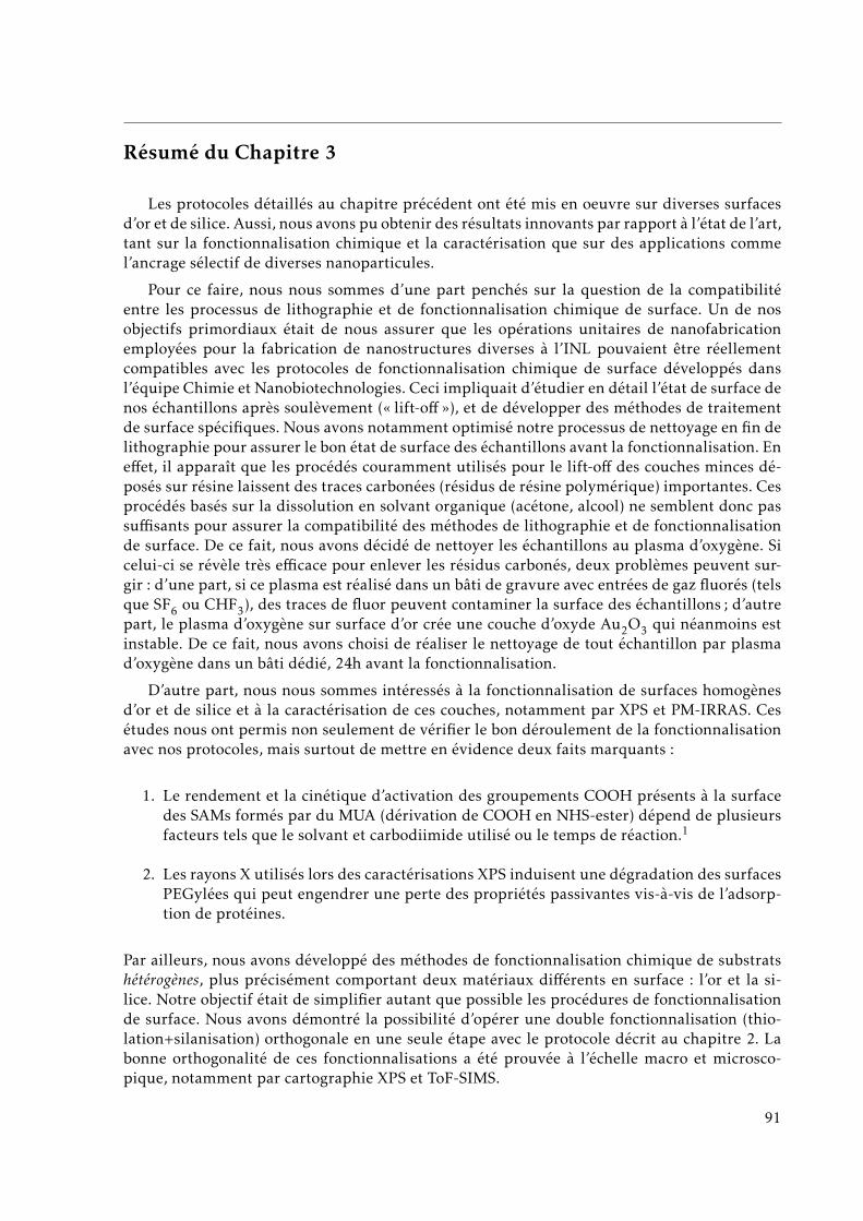
Résumé du Chapitre 3
Les protocoles détaillés au chapitre précédent ont été mis en oeuvre sur diverses surfacesd’or et de silice. Aussi, nous avons pu obtenir des résultats innovants par rapport à l’état de l’art,tant sur la fonctionnalisation chimique et la caractérisation que sur des applications commel’ancrage sélectif de diverses nanoparticules.
Pour ce faire, nous nous sommes d’une part penchés sur la question de la compatibilitéentre les processus de lithographie et de fonctionnalisation chimique de surface. Un de nosobjectifs primordiaux était de nous assurer que les opérations unitaires de nanofabricationemployées pour la fabrication de nanostructures diverses à l’INL pouvaient être réellementcompatibles avec les protocoles de fonctionnalisation chimique de surface développés dansl’équipe Chimie et Nanobiotechnologies. Ceci impliquait d’étudier en détail l’état de surface denos échantillons après soulèvement (« lift-off »), et de développer des méthodes de traitementde surface spécifiques. Nous avons notamment optimisé notre processus de nettoyage en fin delithographie pour assurer le bon état de surface des échantillons avant la fonctionnalisation. Eneffet, il apparaît que les procédés couramment utilisés pour le lift-off des couches minces dé-posés sur résine laissent des traces carbonées (résidus de résine polymérique) importantes. Cesprocédés basés sur la dissolution en solvant organique (acétone, alcool) ne semblent donc passuffisants pour assurer la compatibilité des méthodes de lithographie et de fonctionnalisationde surface. De ce fait, nous avons décidé de nettoyer les échantillons au plasma d’oxygène. Sicelui-ci se révèle très efficace pour enlever les résidus carbonés, deux problèmes peuvent sur-gir : d’une part, si ce plasma est réalisé dans un bâti de gravure avec entrées de gaz fluorés (telsque SF6 ou CHF3), des traces de fluor peuvent contaminer la surface des échantillons ; d’autrepart, le plasma d’oxygène sur surface d’or crée une couche d’oxyde Au2O3 qui néanmoins estinstable. De ce fait, nous avons choisi de réaliser le nettoyage de tout échantillon par plasmad’oxygène dans un bâti dédié, 24h avant la fonctionnalisation.
D’autre part, nous nous sommes intéressés à la fonctionnalisation de surfaces homogènesd’or et de silice et à la caractérisation de ces couches, notamment par XPS et PM-IRRAS. Cesétudes nous ont permis non seulement de vérifier le bon déroulement de la fonctionnalisationavec nos protocoles, mais surtout de mettre en évidence deux faits marquants :
1. Le rendement et la cinétique d’activation des groupements COOH présents à la surfacedes SAMs formés par du MUA (dérivation de COOH en NHS-ester) dépend de plusieursfacteurs tels que le solvant et carbodiimide utilisé ou le temps de réaction.1
2. Les rayons X utilisés lors des caractérisations XPS induisent une dégradation des surfacesPEGylées qui peut engendrer une perte des propriétés passivantes vis-à-vis de l’adsorp-tion de protéines.
Par ailleurs, nous avons développé des méthodes de fonctionnalisation chimique de substratshétérogènes, plus précisément comportant deux matériaux différents en surface : l’or et la si-lice. Notre objectif était de simplifier autant que possible les procédures de fonctionnalisationde surface. Nous avons démontré la possibilité d’opérer une double fonctionnalisation (thio-lation+silanisation) orthogonale en une seule étape avec le protocole décrit au chapitre 2. Labonne orthogonalité de ces fonctionnalisations a été prouvée à l’échelle macro et microsco-pique, notamment par cartographie XPS et ToF-SIMS.
91

Chapter 3. Results and discussion
Enfin, nous avons mis à profit la fonctionnalisation sélective de micro et nanostructuresd’or sur silice, afin de capturer des nanoparticules de latex sur les micro et/ou nanostructuresd’or. Ces captures sélectives ont été menées en nous appuyant uniquement sur les interac-tions entre particules et surfaces fonctionalisées, sans emploi de pince optique ou autre champde force externe. Nous avons prouvé que cette méthode permet le piégeage sélectif sur desmatrices de nanostructures uniques qui sont conçues pour avoir des effets de nano-antennesplasmoniques.2
92

3.1. Surface preconditioning
Introduction to Chapter 3
This chapter presents the main results of this thesis. First we will deal with the study ofthe surface prior to functionalization, specially focussing on the removal of lithography re-sist residues. Then we will present different results obtained with single functionalizations onplain gold or silica substrates. These results include the optimization of the NHS activation ofMUA SAMs1 and the study of PEG degradation under X-rays used during XPS characterization.Furthermore, we will present chemical characterizations to prove the orthogonal functionali-zations of macro and micropatterned gold/silica substrates. Eventually, we will demonstratehow the selective functionalization of gold micro and nanopatterns on silica allows the precisetrapping of different latex nanoparticles.
3.1 Surface preconditioning
Before performing surface chemical functionalizations it is important to know the state ofthe surface. Specially for substrates that have undergone some top-down fabrication steps, itis important to ensure that the surfaces are clean (eg : no photo or e-beam polymeric resistsresidues). We have therefore tested different cleaning procedures whose performances will bediscussed hereafter, along with possible side-effects. Eventually gold surfaces were characteri-zed in regards to their roughness and crystallinity.
3.1.1 Cleaning and (de)oxidation
Before performing surface chemical functionalizations, we must ensure that the surface isappropriately clean. However, surfaces that have undergone lithography processes involvingthe spin-coating and baking of different polymeric resists may yield residual carbon pollu-tions.3 Different approaches can be used to remove such residues, some of which are summa-rized in appendix A.1.2. For simplicity and availability, we decided to investigate approachesbased on organic solvents and on oxygen plasma. 15
In order to test the efficiency and side-effects of different cleaning procedures, we spin-coated and baked PMMA e-beam resist on silica surfaces. We then removed the resist with thedifferent procedures (dissolution in organic solvents or plasma ashing) and assessed the state ofthe surface by XPS. Figure 3.1 shows the results of such procedures which can be summarizedas follows :
– Organic solvents (acetone + alcohol) could not efficiently remove the polymeric resist.Indeed, high amounts of carbon can be seen on the surface, as evidenced by the C1s peakat 285eV (see Fig. 3.1, top spectrum).
– Plasma ashing conducted in a Reactive Ion Etching (RIE) machine efficiently removedPMMA (low C1s intensity) but left fluorine residues as evidenced by the F1s and FKLLpeaks (see Fig. 3.1, middle spectrum). These residues probably come from the use offluorinated gases such as SF6 or CHF3 in the RIE chamber, though these gases were notused here.
15. Piranha solution is often used, specially for uniform surfaces such as plain glass slides. However, previousexperiences in the lab have lead to delamination of gold thin films and nanostructures, so that piranha cleaningwas dismissed for the present work. UV/ozone was also tested in conjunction with the work of Alice Goudot, PhDstudent at that time. However, as it did not prove to give better results than oxygen plasma, it was not used further.
93
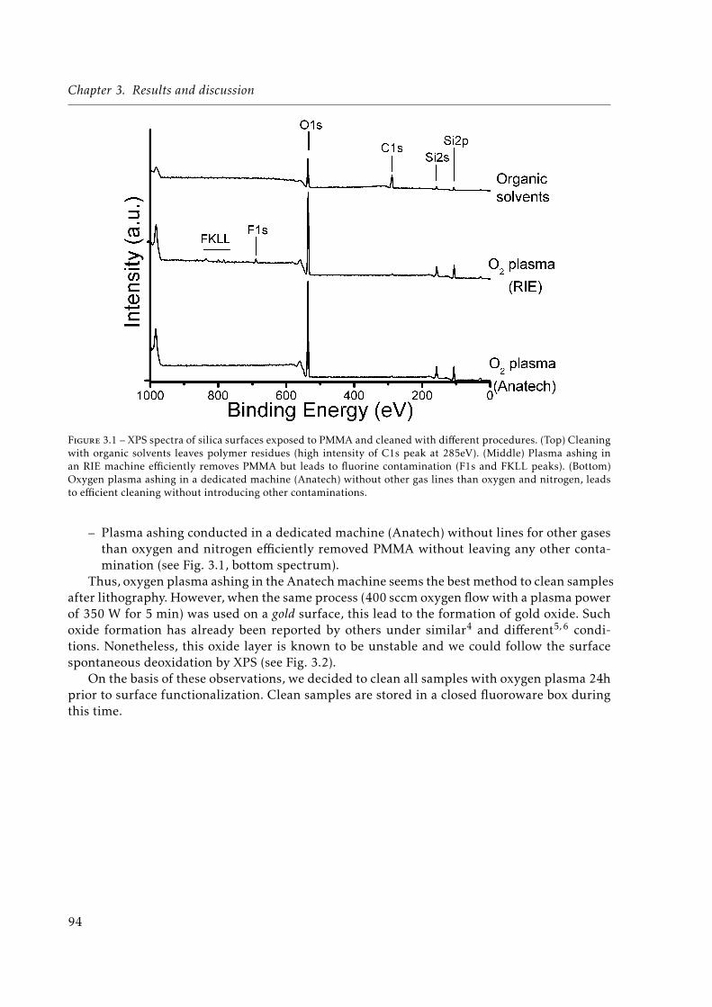
Chapter 3. Results and discussion
Figure 3.1 – XPS spectra of silica surfaces exposed to PMMA and cleaned with different procedures. (Top) Cleaningwith organic solvents leaves polymer residues (high intensity of C1s peak at 285eV). (Middle) Plasma ashing inan RIE machine efficiently removes PMMA but leads to fluorine contamination (F1s and FKLL peaks). (Bottom)Oxygen plasma ashing in a dedicated machine (Anatech) without other gas lines than oxygen and nitrogen, leadsto efficient cleaning without introducing other contaminations.
– Plasma ashing conducted in a dedicated machine (Anatech) without lines for other gasesthan oxygen and nitrogen efficiently removed PMMA without leaving any other conta-mination (see Fig. 3.1, bottom spectrum).
Thus, oxygen plasma ashing in the Anatech machine seems the best method to clean samplesafter lithography. However, when the same process (400 sccm oxygen flow with a plasma powerof 350 W for 5 min) was used on a gold surface, this lead to the formation of gold oxide. Suchoxide formation has already been reported by others under similar4 and different5, 6 condi-tions. Nonetheless, this oxide layer is known to be unstable and we could follow the surfacespontaneous deoxidation by XPS (see Fig. 3.2).
On the basis of these observations, we decided to clean all samples with oxygen plasma 24hprior to surface functionalization. Clean samples are stored in a closed fluoroware box duringthis time.
94
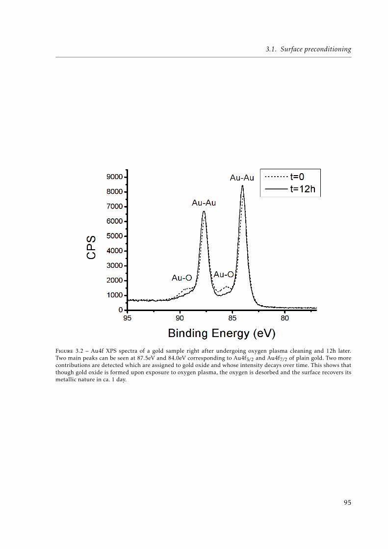
3.1. Surface preconditioning
Figure 3.2 – Au4f XPS spectra of a gold sample right after undergoing oxygen plasma cleaning and 12h later.Two main peaks can be seen at 87.5eV and 84.0eV corresponding to Au4f5/2 and Au4f7/2 of plain gold. Two morecontributions are detected which are assigned to gold oxide and whose intensity decays over time. This shows thatthough gold oxide is formed upon exposure to oxygen plasma, the oxygen is desorbed and the surface recovers itsmetallic nature in ca. 1 day.
95
Chapter 3. Results and discussion
3.1.2 Roughness and crystallinity of deposited gold
We investigated the roughness and crystallinity of the deposited gold thin films (ca. 50nmby e-beam evaporation on silica, with an adhesion interlayer of chromium or titanium of ca.1-3nm). AFM characterization (see Fig. 3.3a) shows that the surface topography of such de-posited gold layers is formed by islands having a width of ca. 50-100nm and heights of ca.4-8nm. The Root Mean Square (RMS) rugosity was found to be around 0.7-1nm. This rugo-sity was confirmed by X-ray reflectivity measurements (data not shown) and does not seem tobe significantly altered by the cleaning method (e.g., oxygen plasma). This surface topogra-phy suggests that it would be difficult to obtain information on SAMs built on such surfacesthrough topography as the SAMs are expected to be on the order of 1nm thick. Indeed, if topo-graphy is used to obtain information on such SAMs in the literature, the gold layer is usuallymade to be atomically flat,7 which greatly departs from our case. Moreover XRD characteriza-tion showed a unique (111) crystalline orientation (see Fig. 3.3b) with grain size in the order offew tens of nanometers, obtained through Scherrer’s formula applied to the XRD (111) peak.The (111) gold crystalline orientation is the most widely studied for the formation of thiolateSAMs and most fundamental characteristics of these SAMs described in section 1.2.1.3.2 (e.g.,chain orientation and packing density) imply such orientation, though some studies also dealwith thiolate SAMs on other crystalline orientations such as (100).8, 9
(a) AFM topography image on a gold surface deposi-ted by evaporation (50 nm) onto silica with a chromiumadhesion interlayer (2 nm).
(b) XRD characterization of gold surface showing aunique (111) orientation revealed by the peak at 2θ =38◦
Figure 3.3 – Gold surface roughness (a) and crystallinity (b)
3.2 Plain substrate functionalizations
Before working on patterned gold/silica substrates, we investigated the functionalizationof plain gold and silica. This allowed us in the first place to evidence the formation of differentSAMs on these surfaces (see sections 3.2.1.1 and 3.2.2). Most importantly, it allowed us to op-timize the NHS activation protocol on MUA SAMs (section 3.2.1.2) and study the degradationof different PEGylated surfaces upon exposure to X-rays during XPS analysis (section 3.2.3).
96
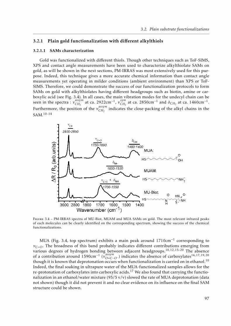
3.2. Plain substrate functionalizations
3.2.1 Plain gold functionalization with different alkylthiols
3.2.1.1 SAMs characterization
Gold was functionalized with different thiols. Though other techniques such as ToF-SIMS,XPS and contact angle measurements have been used to characterize alkylthiolate SAMs ongold, as will be shown in the next sections, PM-IRRAS was most extensively used for this pur-pose. Indeed, this technique gives a more accurate chemical information than contact anglemeasurements yet operating in milder conditions (ambient environment) than XPS or ToF-SIMS. Therefore, we could demonstrate the success of our functionalization protocols to formSAMs on gold with alkylthiolates having different headgroups such as biotin, amine or car-boxylic acid (see Fig. 3.4). In all cases, the main vibration modes for the undecyl chain can beseen in the spectra : νassymCH2
at ca. 2922cm−1, νsymCH2at ca. 2850cm−1 and δCH2
at ca. 1460cm−1.
Furthermore, the position of the νassymCH2indicates the close-packing of the alkyl chains in the
SAM.10–14
Figure 3.4 – PM-IRRAS spectra of MU-Biot, MUAM and MUA SAMs on gold. The most relevant infrared peaksof each molecules can be clearly identified on the corresponding spectrum, showing the success of the chemicalfunctionalizations.
MUA (Fig. 3.4, top spectrum) exhibits a main peak around 1710cm−1 corresponding toνC=O. The broadness of this band probably indicates different contributions emerging fromvarious degrees of hydrogen bonding between adjacent headgroups.10, 12, 15–20 The absenceof a contribution around 1590cm−1 (νassymO=C−O−) indicates the absence of carboxylates16, 17, 19, 20
though it is known that deprotonation occurs when functionalization is carried on in ethanol.10
Indeed, the final soaking in ultrapure water of the MUA-functionalized samples allows for there-protonation of carboxylates into carboxylic acids.17 We also found that carrying the functio-nalization in an ethanol/water mixture (95/5 v/v) slowed the rate of MUA deprotonation (datanot shown) though it did not prevent it and no clear evidence on its influence on the final SAMstructure could be shown.
97
Chapter 3. Results and discussion
MUAM (Fig. 3.4, middle spectrum) shows typical vibration modes associated with δNHat ca. 1650cm−1 and 1530cm−1. These bands are associated with the protonated form of theprimary amine headgroup (NH+
3 ).21
MU-Biot (Fig. 3.4, bottom spectrum) exhibits two dominant peaks at ca. 1690cm−1 and1550cm−1 which correspond to amide I and amide II vibrations.12, 22, 23
3.2.1.2 NHS-ester activation of MUA-functionalized gold
NB : The following paragraphs are adapted from our previous publication.1
Among the different head groups available for immobilizing biomolecules, carboxylic acids(COOH) are commonly chosen for their ability to bind amine groups (NH2) that are presentin proteins, peptides or amino-functionalized oligonucleotides (eg : DNA, RiboNucleic Acid(RNA) or aptamers). COOH and NH2, being oppositely charged in most biological buffers suchas PBS 1X (pH=7.4), can interact electrostatically without further derivatization. However, ifcovalent binding is desired, it is necessary to activate the COOH groups. Activation commonlyconsists of forming a reactive NHS-ester by a two-step reaction between the acid and a carbo-diimide to form O-acylurea followed by a reaction between O-acylurea and NHS to yield theactivated NHS-ester24 (see Scheme 3.1).
Given the widespread use of this methodology,12, 25–31 it could be thought that a well-established protocol leading to efficient activation exists. However, as noted by others,24 animportant number of parameters vary greatly between studies. Indeed, activation may be per-formed in water with EDC12, 25–28 but also in organic solvents such as DiMethyl SulfOxide(DMSO)29 or THF30 with other carbodiimides such as N,N’-DiCyclohexylCarbodiimide (DCC)29, 31
or DIC.30 Carbodiimide and NHS concentrations as well as activation time are also found tovary greatly.23, 25, 29 Furthermore, there is often no chemical characterization at this stage toprove the efficiency of the activation process. It should be noted that achieving the immobi-lization of a protein does not constitute a proof of an efficient activation, as proteins can beeasily physisorbed and may actually bind to a greater extent on non-activated COOH ratherthan on NHS-ester.32
Recent publications24, 33, 34 have highlighted the fact that activation of carboxylic acids onSAMs is a complex reaction (see Scheme 3.2) which can lead not only to the desired NHS-esterformation (reaction (3)) but also to different byproducts such as N-acylurea (reaction (1)) oranhydrides (reaction (2)) :
In addition to the different possible reactions reported in Scheme 3.2, it should be notedthat hydrolysis of different species can furthermore complexify the overall reaction scheme.Most importantly, carboxylic acids can be regenerated at the surface through the hydrolysis ofO-acylurea35 or NHS-ester.36 Additionally the hydrolysis of carbodiimides and O-acylurea canalso produce other byproducts such as urea derivatives.35, 37
Sam et al.24 showed the impact of EDC and NHS concentration on the efficiency of theactivation process and the appearance of the aforementioned byproducts, with a systematicinfrared characterization of the different terminal groups at the surface, albeit not providinginformation about the kinetics of the different reactions.
ToF-SIMS and PM-IRRAS are surface-sensitive methods specially suited for this study. In-deed, as shown by Frey et al.23 the activation process can be monitored by the presence of aninfrared absorption peak at ca. 1820cm−1. It should be noted that during the activation, otherbands appear at ca. 1785cm−1 and 1745cm−1, the latter being the most prominent one. Howe-ver, these two are linked to NHS (be it covalently bonded or just adsorbed) and are thereforenot representative of the activated ester (NHS covalently bonded to the acid head group).
98
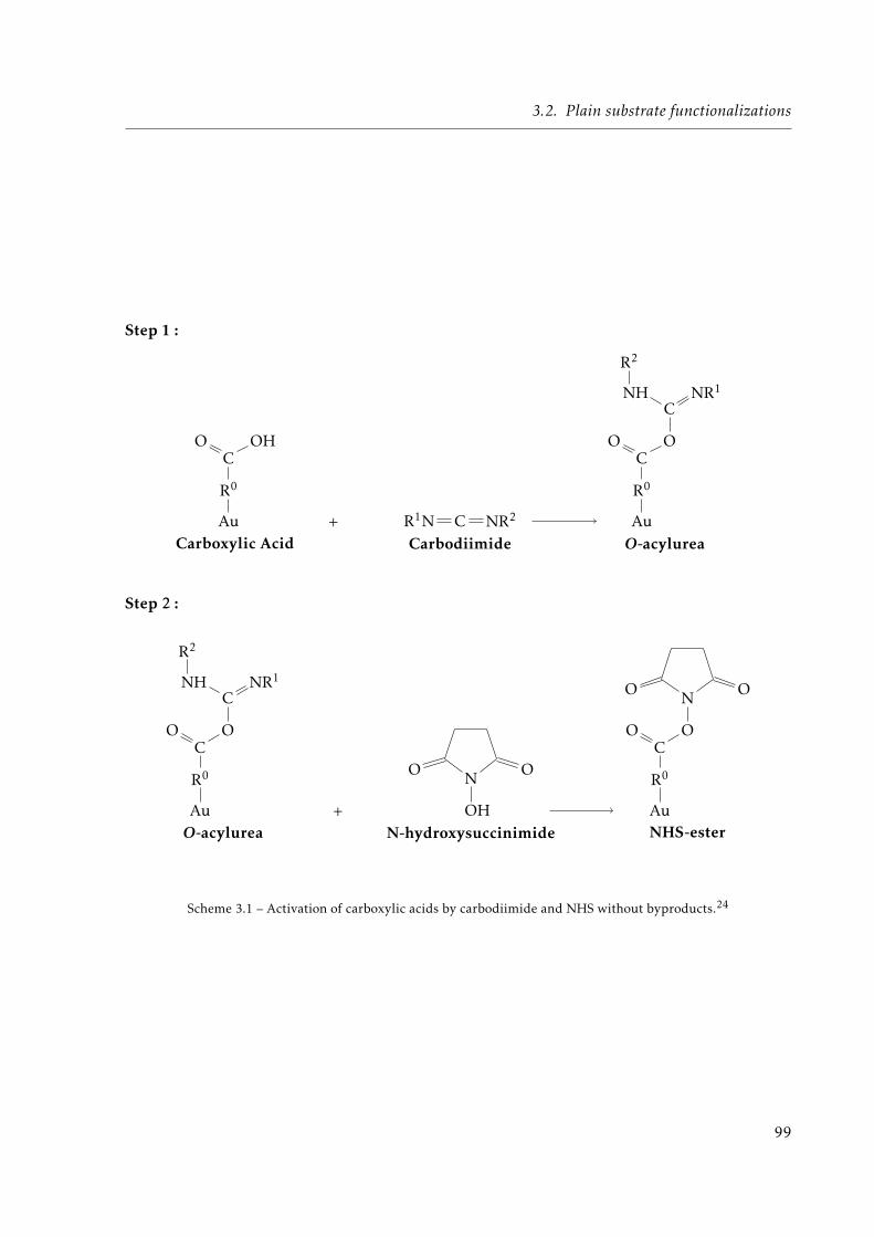
3.2. Plain substrate functionalizations
Step 1 :
Au
R0
CO OH
Carboxylic Acid+ R1N C NR2
CarbodiimideAu
R0
CO O
CHN
R2
NR1
O-acylurea
Step 2 :
Au
R0
CO O
CHN
R2
NR1
O-acylurea+ OH
N OO
N-hydroxysuccinimideAu
R0
CO O
N OO
NHS-ester
Scheme 3.1 – Activation of carboxylic acids by carbodiimide and NHS without byproducts.24
99

Chapter 3. Results and discussion
Au
R0
CO O
CHN
R2
NR1
O-acylurea
(1)
Au
R0
CO NR1
CHN
R2
O
N-acylurea
(2)
Au
R0
CO O
CO
R0
AuAnhydride
(3)+NHS
Au
R0
CO O
N OO
NHS-ester
(4)
+N
HS
Scheme 3.2 – Possible derivatizations of O-acylurea in the presence of NHS, including the expected NHS-ester andmain byproducts : N-acylurea and anhydride.24
100
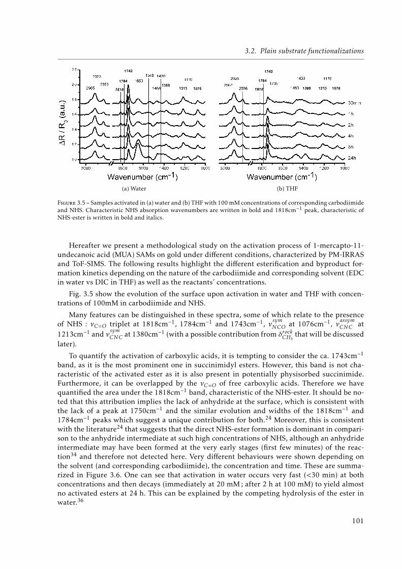
3.2. Plain substrate functionalizations
(a) Water (b) THF
Figure 3.5 – Samples activated in (a) water and (b) THF with 100 mM concentrations of corresponding carbodiimideand NHS. Characteristic NHS absorption wavenumbers are written in bold and 1818cm−1 peak, characteristic ofNHS-ester is written in bold and italics.
Hereafter we present a methodological study on the activation process of 1-mercapto-11-undecanoic acid (MUA) SAMs on gold under different conditions, characterized by PM-IRRASand ToF-SIMS. The following results highlight the different esterification and byproduct for-mation kinetics depending on the nature of the carbodiimide and corresponding solvent (EDCin water vs DIC in THF) as well as the reactants’ concentrations.
Fig. 3.5 show the evolution of the surface upon activation in water and THF with concen-trations of 100mM in carbodiimide and NHS.
Many features can be distinguished in these spectra, some of which relate to the presenceof NHS : νC=O triplet at 1818cm−1, 1784cm−1 and 1743cm−1, νsymNCO at 1076cm−1, νassymCNC at1213cm−1 and νsymCNC at 1380cm−1 (with a possible contribution from δrockCH3
that will be discussedlater).
To quantify the activation of carboxylic acids, it is tempting to consider the ca. 1743cm−1
band, as it is the most prominent one in succinimidyl esters. However, this band is not cha-racteristic of the activated ester as it is also present in potentially physisorbed succinimide.Furthermore, it can be overlapped by the νC=O of free carboxylic acids. Therefore we havequantified the area under the 1818cm−1 band, characteristic of the NHS-ester. It should be no-ted that this attribution implies the lack of anhydride at the surface, which is consistent withthe lack of a peak at 1750cm−1 and the similar evolution and widths of the 1818cm−1 and1784cm−1 peaks which suggest a unique contribution for both.24 Moreover, this is consistentwith the literature24 that suggests that the direct NHS-ester formation is dominant in compari-son to the anhydride intermediate at such high concentrations of NHS, although an anhydrideintermediate may have been formed at the very early stages (first few minutes) of the reac-tion34 and therefore not detected here. Very different behaviours were shown depending onthe solvent (and corresponding carbodiimide), the concentration and time. These are summa-rized in Figure 3.6. One can see that activation in water occurs very fast (<30 min) at bothconcentrations and then decays (immediately at 20 mM ; after 2 h at 100 mM) to yield almostno activated esters at 24 h. This can be explained by the competing hydrolysis of the ester inwater.36
101
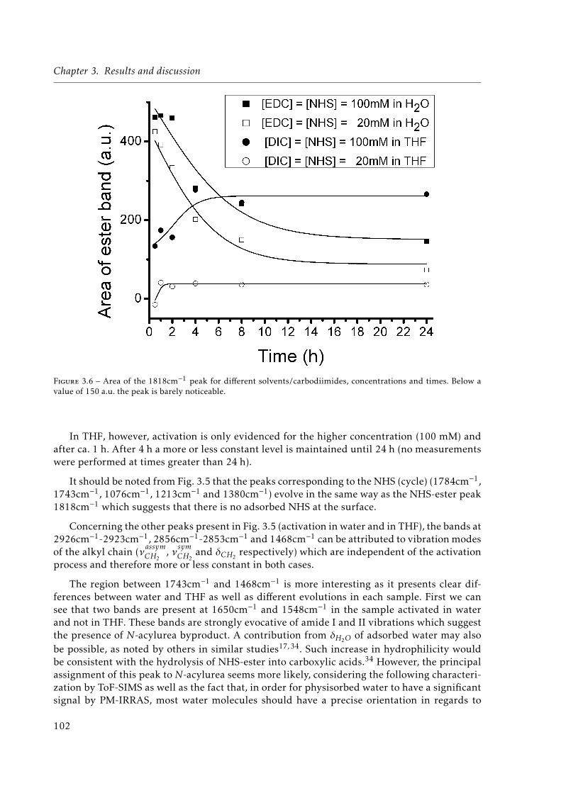
Chapter 3. Results and discussion
Figure 3.6 – Area of the 1818cm−1 peak for different solvents/carbodiimides, concentrations and times. Below avalue of 150 a.u. the peak is barely noticeable.
In THF, however, activation is only evidenced for the higher concentration (100 mM) andafter ca. 1 h. After 4 h a more or less constant level is maintained until 24 h (no measurementswere performed at times greater than 24 h).
It should be noted from Fig. 3.5 that the peaks corresponding to the NHS (cycle) (1784cm−1,1743cm−1, 1076cm−1, 1213cm−1 and 1380cm−1) evolve in the same way as the NHS-ester peak1818cm−1 which suggests that there is no adsorbed NHS at the surface.
Concerning the other peaks present in Fig. 3.5 (activation in water and in THF), the bands at2926cm−1-2923cm−1, 2856cm−1-2853cm−1 and 1468cm−1 can be attributed to vibration modesof the alkyl chain (νassymCH2
, νsymCH2and δCH2
respectively) which are independent of the activationprocess and therefore more or less constant in both cases.
The region between 1743cm−1 and 1468cm−1 is more interesting as it presents clear dif-ferences between water and THF as well as different evolutions in each sample. First we cansee that two bands are present at 1650cm−1 and 1548cm−1 in the sample activated in waterand not in THF. These bands are strongly evocative of amide I and II vibrations which suggestthe presence of N-acylurea byproduct. A contribution from δH2O of adsorbed water may alsobe possible, as noted by others in similar studies17, 34. Such increase in hydrophilicity wouldbe consistent with the hydrolysis of NHS-ester into carboxylic acids.34 However, the principalassignment of this peak to N-acylurea seems more likely, considering the following characteri-zation by ToF-SIMS as well as the fact that, in order for physisorbed water to have a significantsignal by PM-IRRAS, most water molecules should have a precise orientation in regards to
102
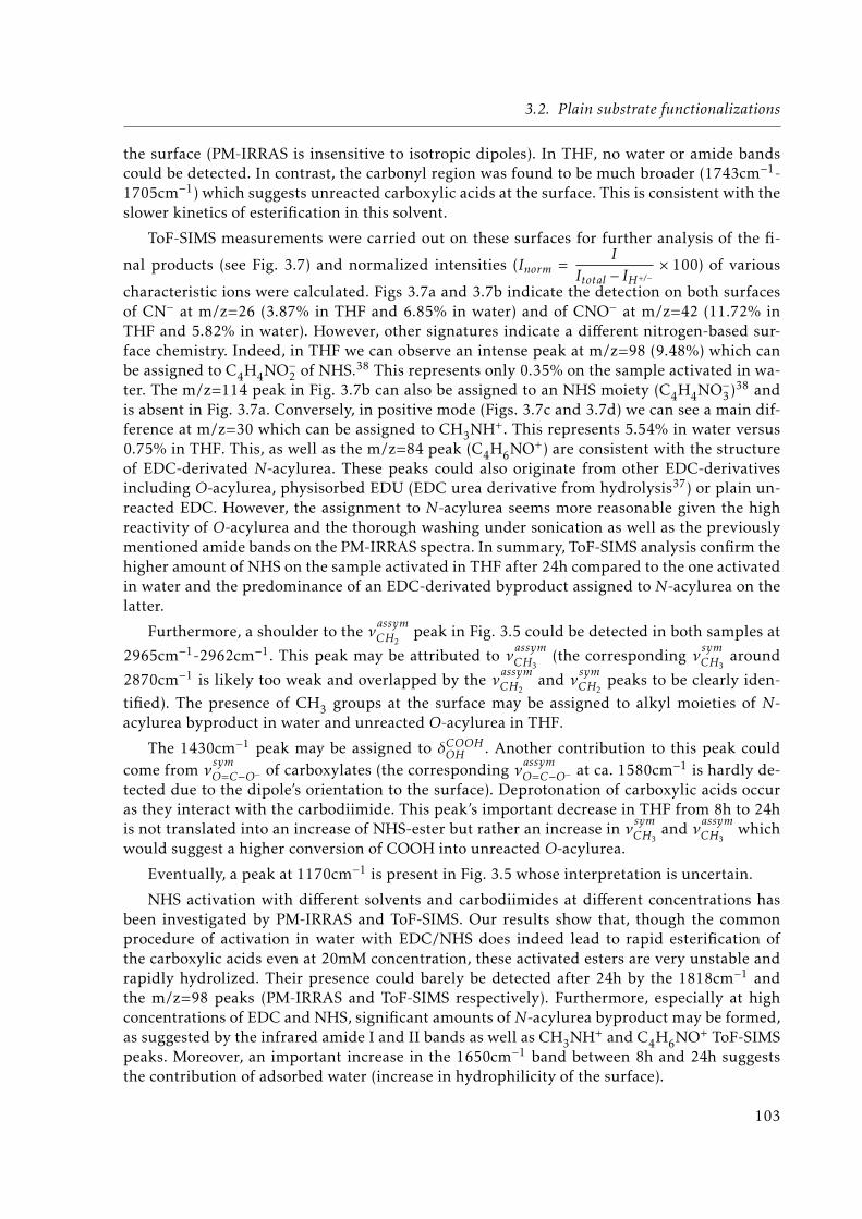
3.2. Plain substrate functionalizations
the surface (PM-IRRAS is insensitive to isotropic dipoles). In THF, no water or amide bandscould be detected. In contrast, the carbonyl region was found to be much broader (1743cm−1-1705cm−1) which suggests unreacted carboxylic acids at the surface. This is consistent with theslower kinetics of esterification in this solvent.
ToF-SIMS measurements were carried out on these surfaces for further analysis of the fi-
nal products (see Fig. 3.7) and normalized intensities (Inorm =I
Itotal − IH+/−× 100) of various
characteristic ions were calculated. Figs 3.7a and 3.7b indicate the detection on both surfacesof CN− at m/z=26 (3.87% in THF and 6.85% in water) and of CNO− at m/z=42 (11.72% inTHF and 5.82% in water). However, other signatures indicate a different nitrogen-based sur-face chemistry. Indeed, in THF we can observe an intense peak at m/z=98 (9.48%) which canbe assigned to C4H4NO−2 of NHS.38 This represents only 0.35% on the sample activated in wa-ter. The m/z=114 peak in Fig. 3.7b can also be assigned to an NHS moiety (C4H4NO−3)38 andis absent in Fig. 3.7a. Conversely, in positive mode (Figs. 3.7c and 3.7d) we can see a main dif-ference at m/z=30 which can be assigned to CH3NH+. This represents 5.54% in water versus0.75% in THF. This, as well as the m/z=84 peak (C4H6NO+) are consistent with the structureof EDC-derivated N-acylurea. These peaks could also originate from other EDC-derivativesincluding O-acylurea, physisorbed EDU (EDC urea derivative from hydrolysis37) or plain un-reacted EDC. However, the assignment to N-acylurea seems more reasonable given the highreactivity of O-acylurea and the thorough washing under sonication as well as the previouslymentioned amide bands on the PM-IRRAS spectra. In summary, ToF-SIMS analysis confirm thehigher amount of NHS on the sample activated in THF after 24h compared to the one activatedin water and the predominance of an EDC-derivated byproduct assigned to N-acylurea on thelatter.
Furthermore, a shoulder to the νassymCH2peak in Fig. 3.5 could be detected in both samples at
2965cm−1-2962cm−1. This peak may be attributed to νassymCH3(the corresponding νsymCH3
around
2870cm−1 is likely too weak and overlapped by the νassymCH2and νsymCH2
peaks to be clearly iden-tified). The presence of CH3 groups at the surface may be assigned to alkyl moieties of N-acylurea byproduct in water and unreacted O-acylurea in THF.
The 1430cm−1 peak may be assigned to δCOOHOH . Another contribution to this peak couldcome from ν
symO=C−O− of carboxylates (the corresponding νassymO=C−O− at ca. 1580cm−1 is hardly de-
tected due to the dipole’s orientation to the surface). Deprotonation of carboxylic acids occuras they interact with the carbodiimide. This peak’s important decrease in THF from 8h to 24his not translated into an increase of NHS-ester but rather an increase in νsymCH3
and νassymCH3which
would suggest a higher conversion of COOH into unreacted O-acylurea.
Eventually, a peak at 1170cm−1 is present in Fig. 3.5 whose interpretation is uncertain.
NHS activation with different solvents and carbodiimides at different concentrations hasbeen investigated by PM-IRRAS and ToF-SIMS. Our results show that, though the commonprocedure of activation in water with EDC/NHS does indeed lead to rapid esterification ofthe carboxylic acids even at 20mM concentration, these activated esters are very unstable andrapidly hydrolized. Their presence could barely be detected after 24h by the 1818cm−1 andthe m/z=98 peaks (PM-IRRAS and ToF-SIMS respectively). Furthermore, especially at highconcentrations of EDC and NHS, significant amounts of N-acylurea byproduct may be formed,as suggested by the infrared amide I and II bands as well as CH3NH+ and C4H6NO+ ToF-SIMSpeaks. Moreover, an important increase in the 1650cm−1 band between 8h and 24h suggeststhe contribution of adsorbed water (increase in hydrophilicity of the surface).
103
Chapter 3. Results and discussion
(a) Water - negative
(b) THF - negative
(c) Water - positive
(d) THF - positive
Figure 3.7 – Negative ((a) and (b)) mode and positive ((c) and (d)) mode ToF-SIMS spectra of samples activatedin water ((a) and (c)) and THF ((b) and (d)) after 24h, in the range of m/z=5-120 (negative mode) and m/z=0-100(positive mode).
104

3.2. Plain substrate functionalizations
In contrast, activation conducted in THF with DIC requires higher concentrations of carbo-diimide and NHS and longer times ; but is more stable, and does not form N-acylurea. Howe-ver, it seems that unreacted O-acylurea remained after 24h, evidenced by the methyl band at2965cm−1-2962cm−1.
105

Chapter 3. Results and discussion
3.2.2 Plain silica functionalization with PEG-silanes
We also investigated the silanization of silica surfaces with PEG-Si to make these surfacesresistant to protein adsorption. Figure 3.8 shows an XPS spectrum of the C1s core-level of aPEGylated silica surface.
Figure 3.8 – C1s XPS spectrum of PEGylated silica surface. Because of the degradation of such molecule underirradiation a single scan is presented instead of the usual co-addition of several scans which, in the absence ofdegradation, would yield a better signal-to-noise ratio.
The spectrum is dominated by a peak at ca. 287eV which can be assigned to the ether car-bons in the OEG chain C-C-O (86.8 % of C1s peak). A second contribution can be detected atca. 285eV corresponding to the propyl chain of the silane, though this contribution is obviouslyfar less intense (13.2 % of C1s peak). The O1s peak is largely dominated by the contribution ofthe silica substrate and therefore not shown here since we could not extract the contributionof the OEG chain. Similarly, no chemical shift could clearly be identified on the Si2s and Si2ppeaks linked to the silanes. The characterization of PEGylated surfaces by XPS led us to an un-planned study of the effects of X-ray irradiation on such organic layers. This study, is presentedin the next section.
3.2.3 Effect of X-rays on PEGylated surfaces
Surfaces modified with OEG and PEG are well known for their antifouling abilities. PEGy-lated gold39, 40 and silica41–45 surfaces are thus widely used in biosensor and microarray tech-nologies, lowering non specific adsorption of interfering species.46, 47 In some circumstances,ethylene glycol moieties can be degraded. Modifications of PEGylated surfaces upon UV orelectronic irradiation have already been described.48–50 PEG can be degraded in ambient at-mosphere by photo-oxydation under UV irradiation, for instance via UV photolithography, ornear-field optical microscopy.48 This causes a cleavage of ether bonds, and yields drastic mo-difications of the PEG film properties, such as antifouling loss. Oxidative degradation of mo-nolayers of OEG-functionalized alkenes on silicon were performed using an AFM probe witha bias potential.49 PEG and Poly(OxyEthylene) (POE) films can also be crosslinked with sub-micrometer resolution under e-beam exposure.51 During XPS analysis, X-rays provide anothertype of irradiation, proven to modify polymers. This is the case with halogenated polymers -
106
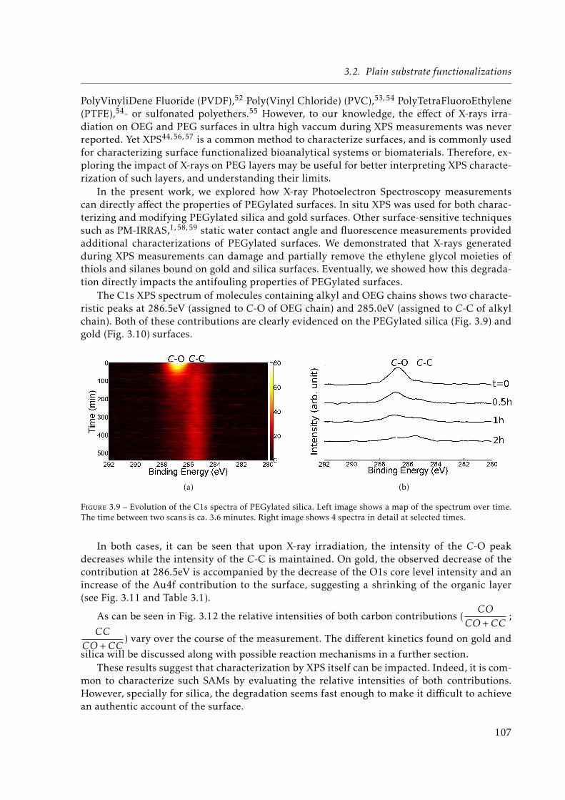
3.2. Plain substrate functionalizations
PolyVinyliDene Fluoride (PVDF),52 Poly(Vinyl Chloride) (PVC),53, 54 PolyTetraFluoroEthylene(PTFE),54- or sulfonated polyethers.55 However, to our knowledge, the effect of X-rays irra-diation on OEG and PEG surfaces in ultra high vaccum during XPS measurements was neverreported. Yet XPS44, 56, 57 is a common method to characterize surfaces, and is commonly usedfor characterizing surface functionalized bioanalytical systems or biomaterials. Therefore, ex-ploring the impact of X-rays on PEG layers may be useful for better interpreting XPS characte-rization of such layers, and understanding their limits.
In the present work, we explored how X-ray Photoelectron Spectroscopy measurementscan directly affect the properties of PEGylated surfaces. In situ XPS was used for both charac-terizing and modifying PEGylated silica and gold surfaces. Other surface-sensitive techniquessuch as PM-IRRAS,1, 58, 59 static water contact angle and fluorescence measurements providedadditional characterizations of PEGylated surfaces. We demonstrated that X-rays generatedduring XPS measurements can damage and partially remove the ethylene glycol moieties ofthiols and silanes bound on gold and silica surfaces. Eventually, we showed how this degrada-tion directly impacts the antifouling properties of PEGylated surfaces.
The C1s XPS spectrum of molecules containing alkyl and OEG chains shows two characte-ristic peaks at 286.5eV (assigned to C-O of OEG chain) and 285.0eV (assigned to C-C of alkylchain). Both of these contributions are clearly evidenced on the PEGylated silica (Fig. 3.9) andgold (Fig. 3.10) surfaces.
(a) (b)
Figure 3.9 – Evolution of the C1s spectra of PEGylated silica. Left image shows a map of the spectrum over time.The time between two scans is ca. 3.6 minutes. Right image shows 4 spectra in detail at selected times.
In both cases, it can be seen that upon X-ray irradiation, the intensity of the C-O peakdecreases while the intensity of the C-C is maintained. On gold, the observed decrease of thecontribution at 286.5eV is accompanied by the decrease of the O1s core level intensity and anincrease of the Au4f contribution to the surface, suggesting a shrinking of the organic layer(see Fig. 3.11 and Table 3.1).
As can be seen in Fig. 3.12 the relative intensities of both carbon contributions (CO
CO+CC;
CCCO+CC
) vary over the course of the measurement. The different kinetics found on gold and
silica will be discussed along with possible reaction mechanisms in a further section.These results suggest that characterization by XPS itself can be impacted. Indeed, it is com-
mon to characterize such SAMs by evaluating the relative intensities of both contributions.However, specially for silica, the degradation seems fast enough to make it difficult to achievean authentic account of the surface.
107
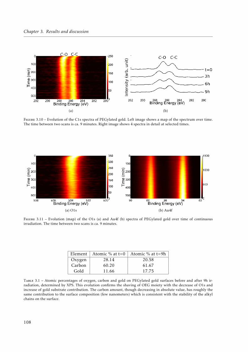
Chapter 3. Results and discussion
(a) (b)
Figure 3.10 – Evolution of the C1s spectra of PEGylated gold. Left image shows a map of the spectrum over time.The time between two scans is ca. 9 minutes. Right image shows 4 spectra in detail at selected times.
(a) O1s (b) Au4f
Figure 3.11 – Evolution (map) of the O1s (a) and Au4f (b) spectra of PEGylated gold over time of continuousirradiation. The time between two scans is ca. 9 minutes.
Element Atomic % at t=0 Atomic % at t=9hOxygen 28.14 20.58Carbon 60.20 61.67
Gold 11.66 17.75
Table 3.1 – Atomic percentages of oxygen, carbon and gold on PEGylated gold surfaces before and after 9h ir-radiation, determined by XPS. This evolution confirms the shaving of OEG moiety with the decrease of O1s andincrease of gold substrate contribution. The carbon amount, though decreasing in absolute value, has roughly thesame contribution to the surface composition (few nanometers) which is consistent with the stability of the alkylchains on the surface.
108
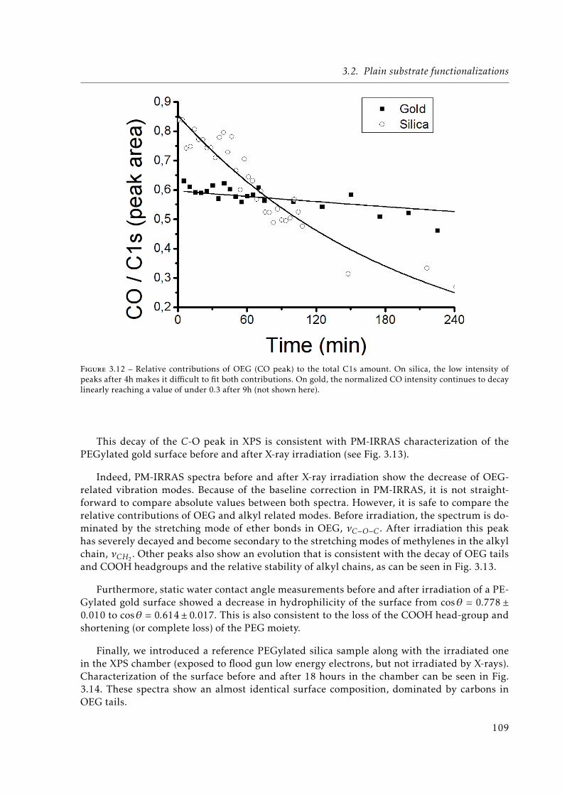
3.2. Plain substrate functionalizations
Figure 3.12 – Relative contributions of OEG (CO peak) to the total C1s amount. On silica, the low intensity ofpeaks after 4h makes it difficult to fit both contributions. On gold, the normalized CO intensity continues to decaylinearly reaching a value of under 0.3 after 9h (not shown here).
This decay of the C-O peak in XPS is consistent with PM-IRRAS characterization of thePEGylated gold surface before and after X-ray irradiation (see Fig. 3.13).
Indeed, PM-IRRAS spectra before and after X-ray irradiation show the decrease of OEG-related vibration modes. Because of the baseline correction in PM-IRRAS, it is not straight-forward to compare absolute values between both spectra. However, it is safe to compare therelative contributions of OEG and alkyl related modes. Before irradiation, the spectrum is do-minated by the stretching mode of ether bonds in OEG, νC−O−C . After irradiation this peakhas severely decayed and become secondary to the stretching modes of methylenes in the alkylchain, νCH2
. Other peaks also show an evolution that is consistent with the decay of OEG tailsand COOH headgroups and the relative stability of alkyl chains, as can be seen in Fig. 3.13.
Furthermore, static water contact angle measurements before and after irradiation of a PE-Gylated gold surface showed a decrease in hydrophilicity of the surface from cosθ = 0.778 ±0.010 to cosθ = 0.614± 0.017. This is also consistent to the loss of the COOH head-group andshortening (or complete loss) of the PEG moiety.
Finally, we introduced a reference PEGylated silica sample along with the irradiated onein the XPS chamber (exposed to flood gun low energy electrons, but not irradiated by X-rays).Characterization of the surface before and after 18 hours in the chamber can be seen in Fig.3.14. These spectra show an almost identical surface composition, dominated by carbons inOEG tails.
109
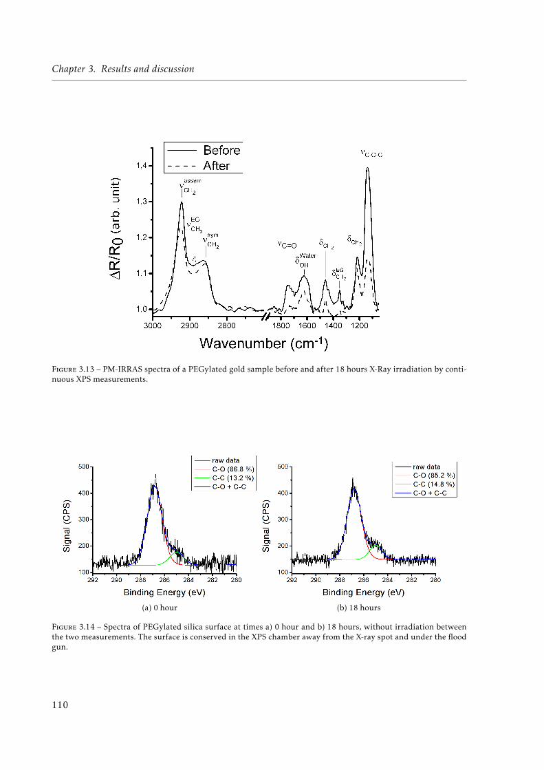
Chapter 3. Results and discussion
Figure 3.13 – PM-IRRAS spectra of a PEGylated gold sample before and after 18 hours X-Ray irradiation by conti-nuous XPS measurements.
(a) 0 hour (b) 18 hours
Figure 3.14 – Spectra of PEGylated silica surface at times a) 0 hour and b) 18 hours, without irradiation betweenthe two measurements. The surface is conserved in the XPS chamber away from the X-ray spot and under the floodgun.
110
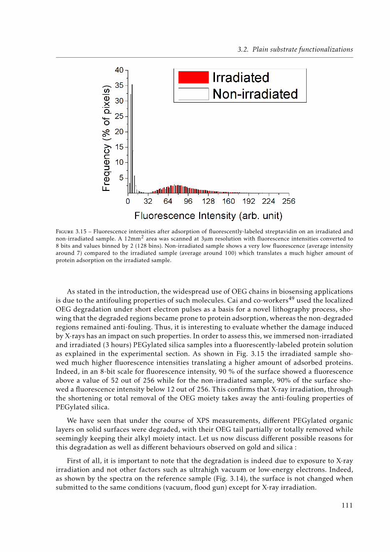
3.2. Plain substrate functionalizations
Figure 3.15 – Fluorescence intensities after adsorption of fluorescently-labeled streptavidin on an irradiated andnon-irradiated sample. A 12mm2 area was scanned at 3µm resolution with fluorescence intensities converted to8 bits and values binned by 2 (128 bins). Non-irradiated sample shows a very low fluorescence (average intensityaround 7) compared to the irradiated sample (average around 100) which translates a much higher amount ofprotein adsorption on the irradiated sample.
As stated in the introduction, the widespread use of OEG chains in biosensing applicationsis due to the antifouling properties of such molecules. Cai and co-workers49 used the localizedOEG degradation under short electron pulses as a basis for a novel lithography process, sho-wing that the degraded regions became prone to protein adsorption, whereas the non-degradedregions remained anti-fouling. Thus, it is interesting to evaluate whether the damage inducedby X-rays has an impact on such properties. In order to assess this, we immersed non-irradiatedand irradiated (3 hours) PEGylated silica samples into a fluorescently-labeled protein solutionas explained in the experimental section. As shown in Fig. 3.15 the irradiated sample sho-wed much higher fluorescence intensities translating a higher amount of adsorbed proteins.Indeed, in an 8-bit scale for fluorescence intensity, 90 % of the surface showed a fluorescenceabove a value of 52 out of 256 while for the non-irradiated sample, 90% of the surface sho-wed a fluorescence intensity below 12 out of 256. This confirms that X-ray irradiation, throughthe shortening or total removal of the OEG moiety takes away the anti-fouling properties ofPEGylated silica.
We have seen that under the course of XPS measurements, different PEGylated organiclayers on solid surfaces were degraded, with their OEG tail partially or totally removed whileseemingly keeping their alkyl moiety intact. Let us now discuss different possible reasons forthis degradation as well as different behaviours observed on gold and silica :
First of all, it is important to note that the degradation is indeed due to exposure to X-rayirradiation and not other factors such as ultrahigh vacuum or low-energy electrons. Indeed,as shown by the spectra on the reference sample (Fig. 3.14), the surface is not changed whensubmitted to the same conditions (vacuum, flood gun) except for X-ray irradiation.
111
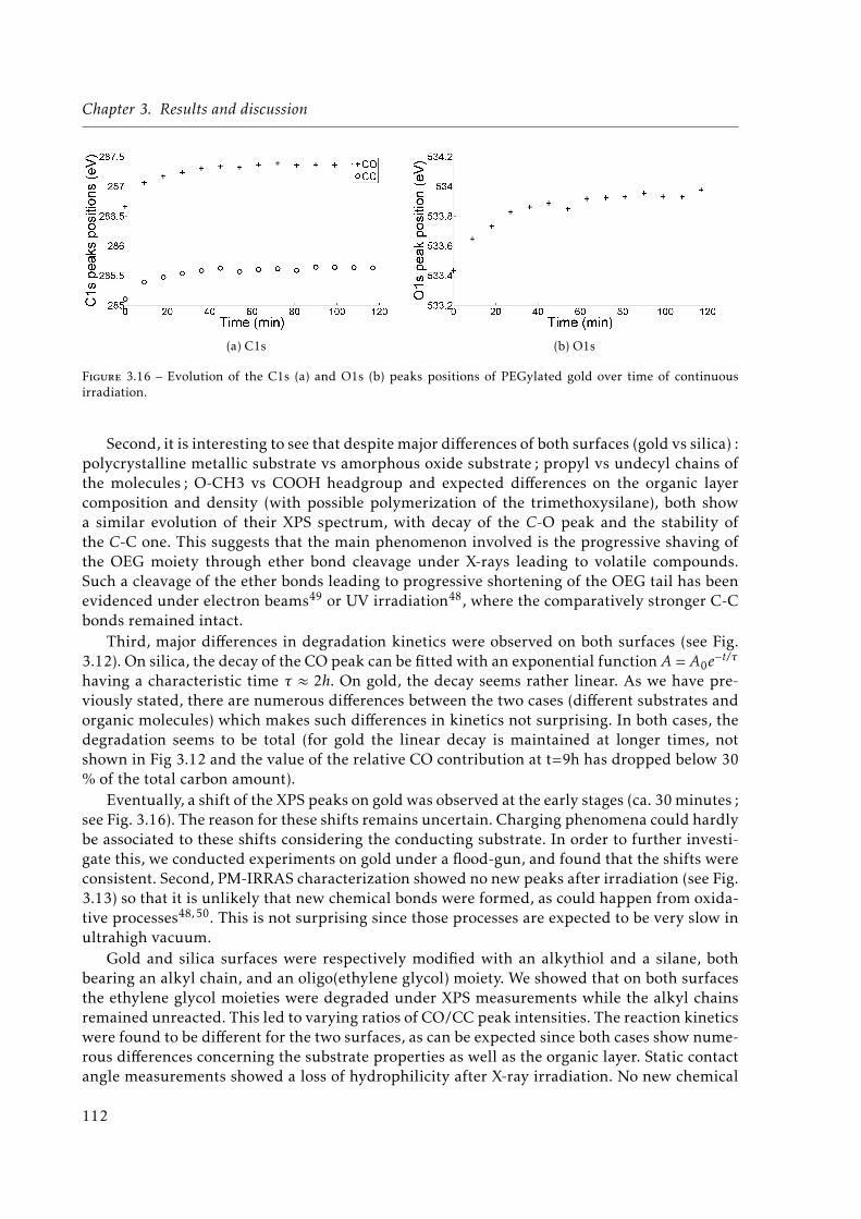
Chapter 3. Results and discussion
(a) C1s (b) O1s
Figure 3.16 – Evolution of the C1s (a) and O1s (b) peaks positions of PEGylated gold over time of continuousirradiation.
Second, it is interesting to see that despite major differences of both surfaces (gold vs silica) :polycrystalline metallic substrate vs amorphous oxide substrate ; propyl vs undecyl chains ofthe molecules ; O-CH3 vs COOH headgroup and expected differences on the organic layercomposition and density (with possible polymerization of the trimethoxysilane), both showa similar evolution of their XPS spectrum, with decay of the C-O peak and the stability ofthe C-C one. This suggests that the main phenomenon involved is the progressive shaving ofthe OEG moiety through ether bond cleavage under X-rays leading to volatile compounds.Such a cleavage of the ether bonds leading to progressive shortening of the OEG tail has beenevidenced under electron beams49 or UV irradiation48, where the comparatively stronger C-Cbonds remained intact.
Third, major differences in degradation kinetics were observed on both surfaces (see Fig.3.12). On silica, the decay of the CO peak can be fitted with an exponential functionA = A0e
−t/τhaving a characteristic time τ ≈ 2h. On gold, the decay seems rather linear. As we have pre-viously stated, there are numerous differences between the two cases (different substrates andorganic molecules) which makes such differences in kinetics not surprising. In both cases, thedegradation seems to be total (for gold the linear decay is maintained at longer times, notshown in Fig 3.12 and the value of the relative CO contribution at t=9h has dropped below 30% of the total carbon amount).
Eventually, a shift of the XPS peaks on gold was observed at the early stages (ca. 30 minutes ;see Fig. 3.16). The reason for these shifts remains uncertain. Charging phenomena could hardlybe associated to these shifts considering the conducting substrate. In order to further investi-gate this, we conducted experiments on gold under a flood-gun, and found that the shifts wereconsistent. Second, PM-IRRAS characterization showed no new peaks after irradiation (see Fig.3.13) so that it is unlikely that new chemical bonds were formed, as could happen from oxida-tive processes48, 50. This is not surprising since those processes are expected to be very slow inultrahigh vacuum.
Gold and silica surfaces were respectively modified with an alkythiol and a silane, bothbearing an alkyl chain, and an oligo(ethylene glycol) moiety. We showed that on both surfacesthe ethylene glycol moieties were degraded under XPS measurements while the alkyl chainsremained unreacted. This led to varying ratios of CO/CC peak intensities. The reaction kineticswere found to be different for the two surfaces, as can be expected since both cases show nume-rous differences concerning the substrate properties as well as the organic layer. Static contactangle measurements showed a loss of hydrophilicity after X-ray irradiation. No new chemical
112
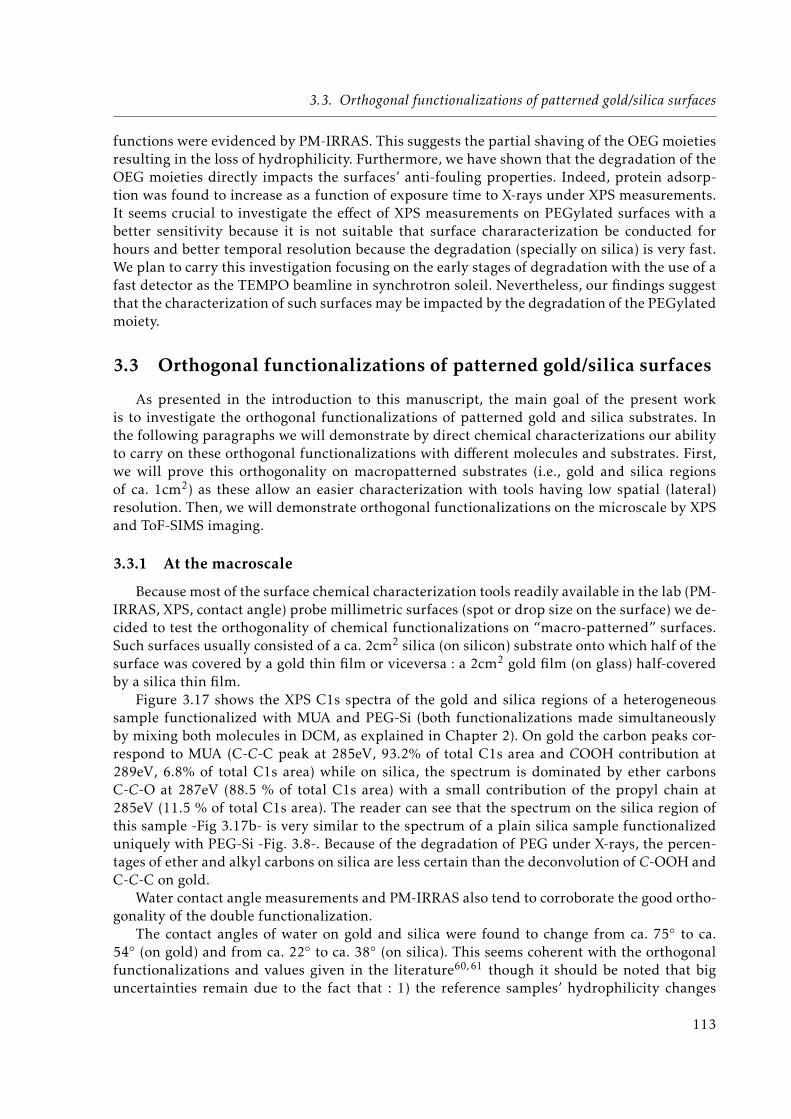
3.3. Orthogonal functionalizations of patterned gold/silica surfaces
functions were evidenced by PM-IRRAS. This suggests the partial shaving of the OEG moietiesresulting in the loss of hydrophilicity. Furthermore, we have shown that the degradation of theOEG moieties directly impacts the surfaces’ anti-fouling properties. Indeed, protein adsorp-tion was found to increase as a function of exposure time to X-rays under XPS measurements.It seems crucial to investigate the effect of XPS measurements on PEGylated surfaces with abetter sensitivity because it is not suitable that surface chararacterization be conducted forhours and better temporal resolution because the degradation (specially on silica) is very fast.We plan to carry this investigation focusing on the early stages of degradation with the use of afast detector as the TEMPO beamline in synchrotron soleil. Nevertheless, our findings suggestthat the characterization of such surfaces may be impacted by the degradation of the PEGylatedmoiety.
3.3 Orthogonal functionalizations of patterned gold/silica surfaces
As presented in the introduction to this manuscript, the main goal of the present workis to investigate the orthogonal functionalizations of patterned gold and silica substrates. Inthe following paragraphs we will demonstrate by direct chemical characterizations our abilityto carry on these orthogonal functionalizations with different molecules and substrates. First,we will prove this orthogonality on macropatterned substrates (i.e., gold and silica regionsof ca. 1cm2) as these allow an easier characterization with tools having low spatial (lateral)resolution. Then, we will demonstrate orthogonal functionalizations on the microscale by XPSand ToF-SIMS imaging.
3.3.1 At the macroscale
Because most of the surface chemical characterization tools readily available in the lab (PM-IRRAS, XPS, contact angle) probe millimetric surfaces (spot or drop size on the surface) we de-cided to test the orthogonality of chemical functionalizations on “macro-patterned” surfaces.Such surfaces usually consisted of a ca. 2cm2 silica (on silicon) substrate onto which half of thesurface was covered by a gold thin film or viceversa : a 2cm2 gold film (on glass) half-coveredby a silica thin film.
Figure 3.17 shows the XPS C1s spectra of the gold and silica regions of a heterogeneoussample functionalized with MUA and PEG-Si (both functionalizations made simultaneouslyby mixing both molecules in DCM, as explained in Chapter 2). On gold the carbon peaks cor-respond to MUA (C-C-C peak at 285eV, 93.2% of total C1s area and COOH contribution at289eV, 6.8% of total C1s area) while on silica, the spectrum is dominated by ether carbonsC-C-O at 287eV (88.5 % of total C1s area) with a small contribution of the propyl chain at285eV (11.5 % of total C1s area). The reader can see that the spectrum on the silica region ofthis sample -Fig 3.17b- is very similar to the spectrum of a plain silica sample functionalizeduniquely with PEG-Si -Fig. 3.8-. Because of the degradation of PEG under X-rays, the percen-tages of ether and alkyl carbons on silica are less certain than the deconvolution of C-OOH andC-C-C on gold.
Water contact angle measurements and PM-IRRAS also tend to corroborate the good ortho-gonality of the double functionalization.
The contact angles of water on gold and silica were found to change from ca. 75◦ to ca.54◦ (on gold) and from ca. 22◦ to ca. 38◦ (on silica). This seems coherent with the orthogonalfunctionalizations and values given in the literature60, 61 though it should be noted that biguncertainties remain due to the fact that : 1) the reference samples’ hydrophilicity changes
113
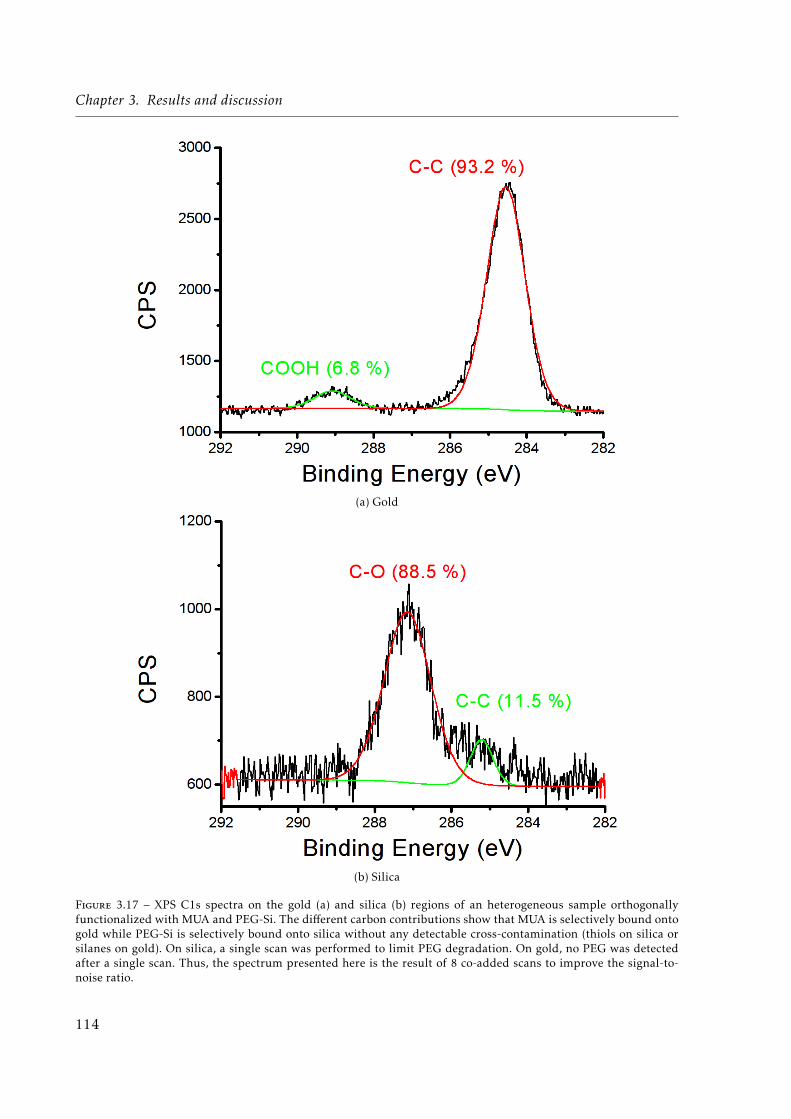
Chapter 3. Results and discussion
(a) Gold
(b) Silica
Figure 3.17 – XPS C1s spectra on the gold (a) and silica (b) regions of an heterogeneous sample orthogonallyfunctionalized with MUA and PEG-Si. The different carbon contributions show that MUA is selectively bound ontogold while PEG-Si is selectively bound onto silica without any detectable cross-contamination (thiols on silica orsilanes on gold). On silica, a single scan was performed to limit PEG degradation. On gold, no PEG was detectedafter a single scan. Thus, the spectrum presented here is the result of 8 co-added scans to improve the signal-to-noise ratio.
114
3.3. Orthogonal functionalizations of patterned gold/silica surfaces
upon ageing (both, gold and silica, are found to be very hydrophilic just after oxygen plasmacleaning but become more hydrophobic in few hours of remaining in a closed box in the lab)and 2) measurements are taken in an uncontrolled environment in regards to humidity andnot finely controlled in regards to temperature.
Regarding PM-IRRAS, we could identify MUA on the gold region (spectrum not shown) butwe were unable to clearly identify the organic layer on silica. It is in principle not impossibleto conduct PM-IRRAS characterization of an organic layer on silica if the silica layer is only athin film on top of a metallic substrate.58 However, one still has to appropriately substract thesilica -dominant- contribution to the spectrum in order to obtain the spectrum of the organicadlayer only. Moreover, the molecular structure of PEG-Si is largely dominated by C−O−Cbonds whose main vibration mode is very close to the main vibration mode of silica Si−O− Sibonds around 1100cm−1. This makes the detection of PEG-Si by PM-IRRAS more difficult thanother silanes58 as the main peak of the organic molecule is drowned inside the signal of theunderlying silica.
Single-step double functionalizations seem to be appropriately orthogonal on average overmacroscopic surfaces. We therefore decided to test the orthogonality of such functionalizationson a smaller scale, which implies the use of different characterization tools as we will see in thenext chapter.
3.3.2 At the microscale
In order to test the orthogonality of single-step double functionalizations on micropatter-ned surfaces, we performed XPS and ToF-SIMS analysis with lateral resolution of few to tenmicrons, with the help of Thierry Le Mogne at LTDS and Didier Léonard at ISA respectively.
Different micropatterned samples were prepared by UV-lithography. The surface of thesesamples yielded gold microsquares of ca. 90µm surrounded by silica lines of equivalent width.We then performed single-step thiolation+silanization of these patterned substrates and che-cked the orthogonality of the functionalizations (presence of the thiol only on the gold micros-quares and presence of the silane only on the silica lines). For an easier analysis we decidedto perform the double functionalizations including a perfluorinated molecule (fluorine being astrong emitter for XPS and ToF-SIMS). Two orthogonal functionalizations were conducted ondifferent micropatterned samples :
1. AuF + PEG-Si
2. SiF + MUA
If the functionalizations are truly orthogonal, we expect to find fluorine only on the goldmicrosquares in the first case (AuF + PEG-Si) and vice-versa in the second (SiF + MUA). Thiswas indeed shown by XPS and ToF-SIMS.
3.3.2.1 XPS analysis
Micropatterned gold on silica substrates functionalized with either (1) AuF and PEG-Sior (2) SiF and MUA were analyzed by XPS. On both surfaces, a first image was acquired byscanning and collecting all secondary electrons (same principle as an SEM). This allows tovisualize the gold microsquares (brighter) and surrounding silica lines (darker) as can be seenin Figs. 3.18 and 3.19. Then, two different regions (ca. 10µm) corresponding to gold and silicasurfaces were selected to perform a “full” spectrum (1000eV-0eV). These spectra show thefollowing :
115
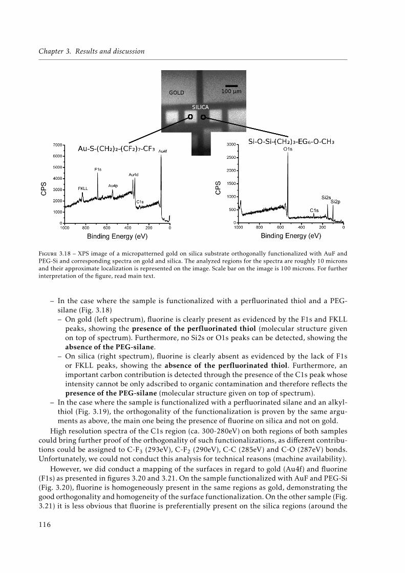
Chapter 3. Results and discussion
Figure 3.18 – XPS image of a micropatterned gold on silica substrate orthogonally functionalized with AuF andPEG-Si and corresponding spectra on gold and silica. The analyzed regions for the spectra are roughly 10 micronsand their approximate localization is represented on the image. Scale bar on the image is 100 microns. For furtherinterpretation of the figure, read main text.
– In the case where the sample is functionalized with a perfluorinated thiol and a PEG-silane (Fig. 3.18)– On gold (left spectrum), fluorine is clearly present as evidenced by the F1s and FKLL
peaks, showing the presence of the perfluorinated thiol (molecular structure givenon top of spectrum). Furthermore, no Si2s or O1s peaks can be detected, showing theabsence of the PEG-silane.
– On silica (right spectrum), fluorine is clearly absent as evidenced by the lack of F1sor FKLL peaks, showing the absence of the perfluorinated thiol. Furthermore, animportant carbon contribution is detected through the presence of the C1s peak whoseintensity cannot be only adscribed to organic contamination and therefore reflects thepresence of the PEG-silane (molecular structure given on top of spectrum).
– In the case where the sample is functionalized with a perfluorinated silane and an alkyl-thiol (Fig. 3.19), the orthogonality of the functionalization is proven by the same argu-ments as above, the main one being the presence of fluorine on silica and not on gold.
High resolution spectra of the C1s region (ca. 300-280eV) on both regions of both samplescould bring further proof of the orthogonality of such functionalizations, as different contribu-tions could be assigned to C-F3 (293eV), C-F2 (290eV), C-C (285eV) and C-O (287eV) bonds.Unfortunately, we could not conduct this analysis for technical reasons (machine availability).
However, we did conduct a mapping of the surfaces in regard to gold (Au4f) and fluorine(F1s) as presented in figures 3.20 and 3.21. On the sample functionalized with AuF and PEG-Si(Fig. 3.20), fluorine is homogeneously present in the same regions as gold, demonstrating thegood orthogonality and homogeneity of the surface functionalization. On the other sample (Fig.3.21) it is less obvious that fluorine is preferentially present on the silica regions (around the
116
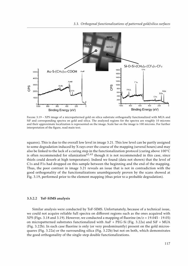
3.3. Orthogonal functionalizations of patterned gold/silica surfaces
Figure 3.19 – XPS image of a micropatterned gold on silica substrate orthogonally functionalized with MUA andSiF and corresponding spectra on gold and silica. The analyzed regions for the spectra are roughly 10 micronsand their approximate localization is represented on the image. Scale bar on the image is 100 microns. For furtherinterpretation of the figure, read main text.
squares). This is due to the overall low level in image 3.21. This low level can be partly assignedto some degradation induced by X-rays over the course of the mapping (several hours) and mayalso be linked to the lack of a curing step in the functionalization protocol (curing above 100◦Cis often recommended for silanization62, 63 though it is not recommended in this case, sincethiols could desorb at high temperature). Indeed we found (data not shown) that the level ofC1s and F1s had dropped on this sample between the beginning and the end of the mapping.Thus, the poor contrast in image 3.21 reveals an issue that is not in contradiction with thegood orthogonality of the functionalizations unambiguously proven by the scans showed atFig. 3.19, performed prior to the element mapping (thus prior to a probable degradation).
3.3.2.2 ToF-SIMS analysis
Similar analysis were conducted by ToF-SIMS. Unfortunately, because of a technical issue,we could not acquire reliable full spectra on different regions such as the ones acquired withXPS (Figs. 3.18 and 3.19). However, we conducted a mapping of fluorine (m/z = 19.045 - 19.05)on micropatterned substrates functionalized with AuF + PEG-Si (Fig. 3.22a) and SiF + MUA(Fig. 3.22b). In each case fluorine is only (or very predominantly) present on the gold micros-quares (Fig. 3.22a) or the surrounding silica (Fig. 3.22b) but not on both, which demonstratesthe good orthogonality of the single-step double functionalizations.
117
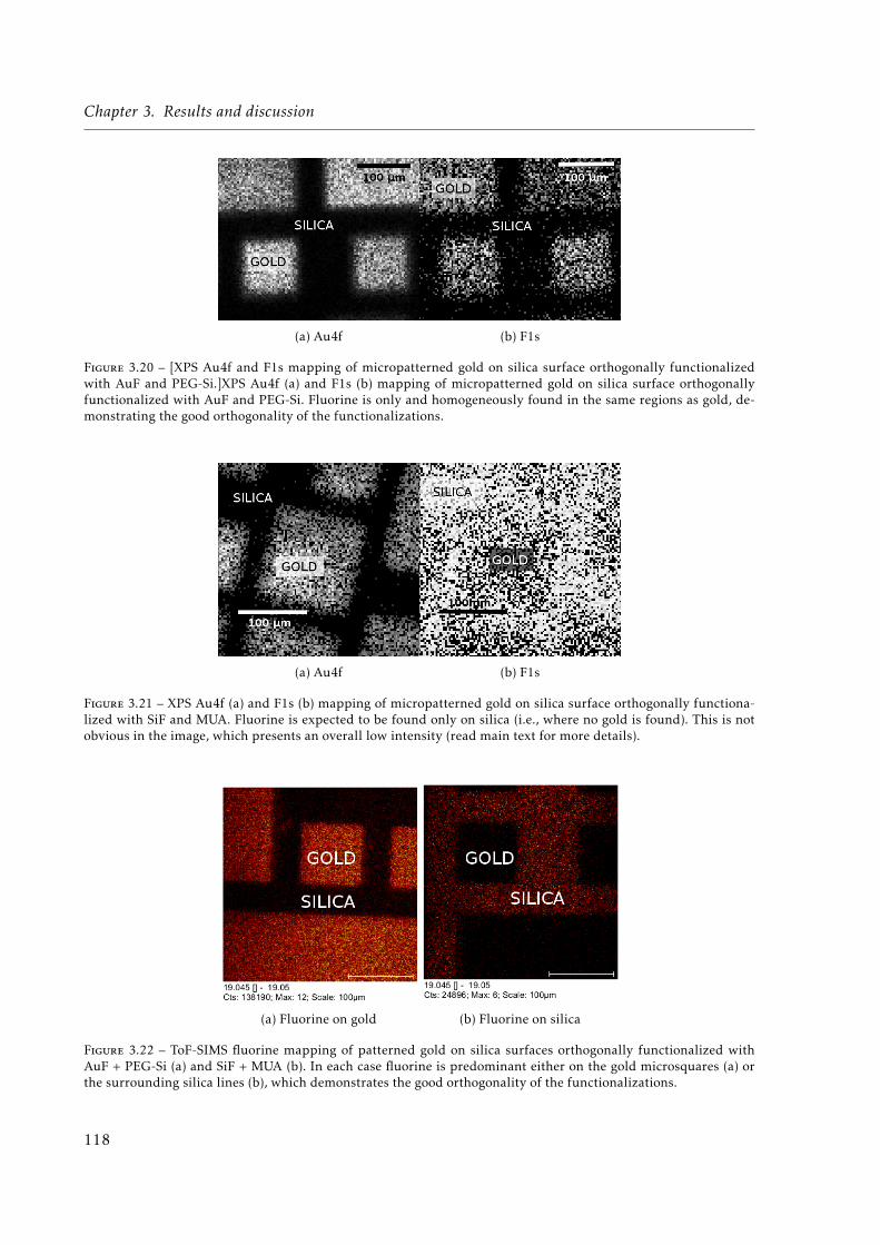
Chapter 3. Results and discussion
(a) Au4f (b) F1s
Figure 3.20 – [XPS Au4f and F1s mapping of micropatterned gold on silica surface orthogonally functionalizedwith AuF and PEG-Si.]XPS Au4f (a) and F1s (b) mapping of micropatterned gold on silica surface orthogonallyfunctionalized with AuF and PEG-Si. Fluorine is only and homogeneously found in the same regions as gold, de-monstrating the good orthogonality of the functionalizations.
(a) Au4f (b) F1s
Figure 3.21 – XPS Au4f (a) and F1s (b) mapping of micropatterned gold on silica surface orthogonally functiona-lized with SiF and MUA. Fluorine is expected to be found only on silica (i.e., where no gold is found). This is notobvious in the image, which presents an overall low intensity (read main text for more details).
(a) Fluorine on gold (b) Fluorine on silica
Figure 3.22 – ToF-SIMS fluorine mapping of patterned gold on silica surfaces orthogonally functionalized withAuF + PEG-Si (a) and SiF + MUA (b). In each case fluorine is predominant either on the gold microsquares (a) orthe surrounding silica lines (b), which demonstrates the good orthogonality of the functionalizations.
118
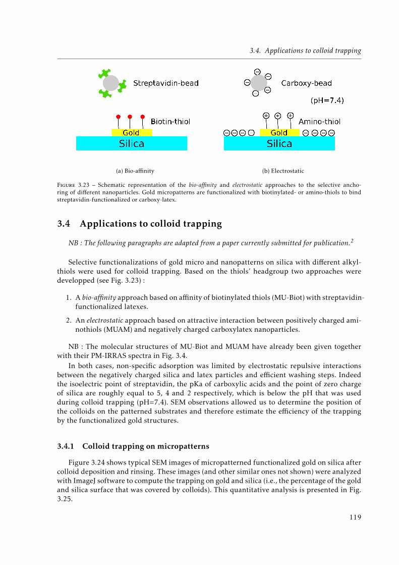
3.4. Applications to colloid trapping
(a) Bio-affinity (b) Electrostatic
Figure 3.23 – Schematic representation of the bio-affinity and electrostatic approaches to the selective ancho-ring of different nanoparticles. Gold micropatterns are functionalized with biotinylated- or amino-thiols to bindstreptavidin-functionalized or carboxy-latex.
3.4 Applications to colloid trapping
NB : The following paragraphs are adapted from a paper currently submitted for publication.2
Selective functionalizations of gold micro and nanopatterns on silica with different alkyl-thiols were used for colloid trapping. Based on the thiols’ headgroup two approaches weredevelopped (see Fig. 3.23) :
1. A bio-affinity approach based on affinity of biotinylated thiols (MU-Biot) with streptavidin-functionalized latexes.
2. An electrostatic approach based on attractive interaction between positively charged ami-nothiols (MUAM) and negatively charged carboxylatex nanoparticles.
NB : The molecular structures of MU-Biot and MUAM have already been given togetherwith their PM-IRRAS spectra in Fig. 3.4.
In both cases, non-specific adsorption was limited by electrostatic repulsive interactionsbetween the negatively charged silica and latex particles and efficient washing steps. Indeedthe isoelectric point of streptavidin, the pKa of carboxylic acids and the point of zero chargeof silica are roughly equal to 5, 4 and 2 respectively, which is below the pH that was usedduring colloid trapping (pH=7.4). SEM observations allowed us to determine the position ofthe colloids on the patterned substrates and therefore estimate the efficiency of the trappingby the functionalized gold structures.
3.4.1 Colloid trapping on micropatterns
Figure 3.24 shows typical SEM images of micropatterned functionalized gold on silica aftercolloid deposition and rinsing. These images (and other similar ones not shown) were analyzedwith ImageJ software to compute the trapping on gold and silica (i.e., the percentage of the goldand silica surface that was covered by colloids). This quantitative analysis is presented in Fig.3.25.
119
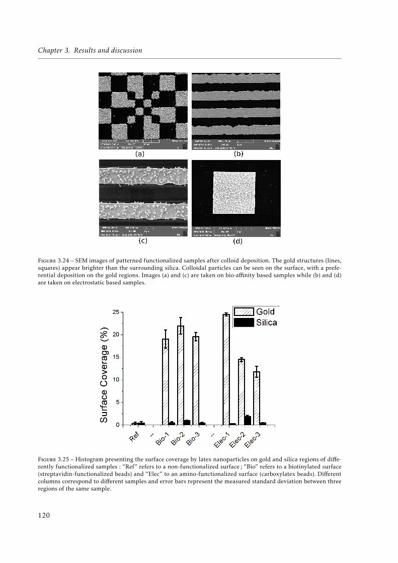
Chapter 3. Results and discussion
Figure 3.24 – SEM images of patterned functionalized samples after colloid deposition. The gold structures (lines,squares) appear brighter than the surrounding silica. Colloidal particles can be seen on the surface, with a prefe-rential deposition on the gold regions. Images (a) and (c) are taken on bio-affinity based samples while (b) and (d)are taken on electrostatic based samples.
Figure 3.25 – Histogram presenting the surface coverage by latex nanoparticles on gold and silica regions of diffe-rently functionalized samples : “Ref” refers to a non-functionalized surface ; “Bio” refers to a biotinylated surface(streptavidin-functionalized beads) and “Elec” to an amino-functionalized surface (carboxylatex beads). Differentcolumns correspond to different samples and error bars represent the measured standard deviation between threeregions of the same sample.
120
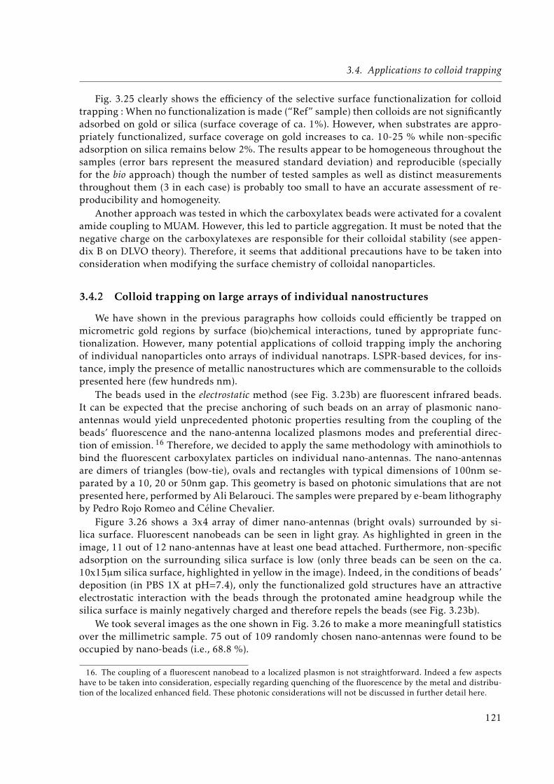
3.4. Applications to colloid trapping
Fig. 3.25 clearly shows the efficiency of the selective surface functionalization for colloidtrapping : When no functionalization is made (“Ref” sample) then colloids are not significantlyadsorbed on gold or silica (surface coverage of ca. 1%). However, when substrates are appro-priately functionalized, surface coverage on gold increases to ca. 10-25 % while non-specificadsorption on silica remains below 2%. The results appear to be homogeneous throughout thesamples (error bars represent the measured standard deviation) and reproducible (speciallyfor the bio approach) though the number of tested samples as well as distinct measurementsthroughout them (3 in each case) is probably too small to have an accurate assessment of re-producibility and homogeneity.
Another approach was tested in which the carboxylatex beads were activated for a covalentamide coupling to MUAM. However, this led to particle aggregation. It must be noted that thenegative charge on the carboxylatexes are responsible for their colloidal stability (see appen-dix B on DLVO theory). Therefore, it seems that additional precautions have to be taken intoconsideration when modifying the surface chemistry of colloidal nanoparticles.
3.4.2 Colloid trapping on large arrays of individual nanostructures
We have shown in the previous paragraphs how colloids could efficiently be trapped onmicrometric gold regions by surface (bio)chemical interactions, tuned by appropriate func-tionalization. However, many potential applications of colloid trapping imply the anchoringof individual nanoparticles onto arrays of individual nanotraps. LSPR-based devices, for ins-tance, imply the presence of metallic nanostructures which are commensurable to the colloidspresented here (few hundreds nm).
The beads used in the electrostatic method (see Fig. 3.23b) are fluorescent infrared beads.It can be expected that the precise anchoring of such beads on an array of plasmonic nano-antennas would yield unprecedented photonic properties resulting from the coupling of thebeads’ fluorescence and the nano-antenna localized plasmons modes and preferential direc-tion of emission. 16 Therefore, we decided to apply the same methodology with aminothiols tobind the fluorescent carboxylatex particles on individual nano-antennas. The nano-antennasare dimers of triangles (bow-tie), ovals and rectangles with typical dimensions of 100nm se-parated by a 10, 20 or 50nm gap. This geometry is based on photonic simulations that are notpresented here, performed by Ali Belarouci. The samples were prepared by e-beam lithographyby Pedro Rojo Romeo and Céline Chevalier.
Figure 3.26 shows a 3x4 array of dimer nano-antennas (bright ovals) surrounded by si-lica surface. Fluorescent nanobeads can be seen in light gray. As highlighted in green in theimage, 11 out of 12 nano-antennas have at least one bead attached. Furthermore, non-specificadsorption on the surrounding silica surface is low (only three beads can be seen on the ca.10x15µm silica surface, highlighted in yellow in the image). Indeed, in the conditions of beads’deposition (in PBS 1X at pH=7.4), only the functionalized gold structures have an attractiveelectrostatic interaction with the beads through the protonated amine headgroup while thesilica surface is mainly negatively charged and therefore repels the beads (see Fig. 3.23b).
We took several images as the one shown in Fig. 3.26 to make a more meaningfull statisticsover the millimetric sample. 75 out of 109 randomly chosen nano-antennas were found to beoccupied by nano-beads (i.e., 68.8 %).
16. The coupling of a fluorescent nanobead to a localized plasmon is not straightforward. Indeed a few aspectshave to be taken into consideration, especially regarding quenching of the fluorescence by the metal and distribu-tion of the localized enhanced field. These photonic considerations will not be discussed in further detail here.
121
Chapter 3. Results and discussion
Figure 3.26 – 3x4 array of dimer nano-antennas with fluorescent nanobeads attached through surface chemicalfunctionalization. 11 out of 12 nano-antennas (green circles) are occupied by one, two or three nanobeads, pre-ferentially anchored at the edges and corners. Only one nano-antenna is found unoccupied (red circle) while lownon-specific adsorption (yellow circles) is found on the surrounding silica.
There are however a certain number of additional issues that become apparent when loo-king more closely at the nanostructures (Fig. 3.27) :
1. At this stage, the metallic dimers do not have the desired geometry. Indeed, it appearsthat some dimers are bridged (Fig. 3.27b) and others have a gap bigger than 50nm (Fig.3.27a).
2. Though it is possible to find a single bead localized on the gap of the dimer (Fig. 3.27a),we generally found 1, 2 (Fig. 3.27b) or 3 (Fig. 3.27c), not necessarily on the gap of thedimer. It does not seem reasonable to think that surface functionalization alone can finelytune the position of the beads on the nanostructures. However, a combination of surfacefunctionalization and photonic approaches64 may overcome this issue.
Furthermore, it must be noted that non-specific adsorption was generally higher that whatcan be seen in Fig. 3.26 although it remained low (few tens of beads on a 10x15µm surface).Mixing and washing procedures will have to be improved in the future, for enabling an homo-geneous behaviour on large areas.
Nonetheless, these results prove that selective surface chemical functionalizations can beused to arrange different colloids onto large arrays of individual nanotraps which may serve as ageneral framework for the development of novel systems combining the physical properties ofnano-objects and the high degree of complexity (miniaturization and diversification) allowedby lithography nanopatterning of a substrate.
122

3.5. Conclusions on the experimental results
(a) Single particle on a bigger thanexpected gap
(b) Two particles captured on abridged “dimer”
(c) Three particles on a dimer andtwo non-specifically adsorbed onsurrounding silica
Figure 3.27 – SEM images of single dimer nano-antennas with trapped nanobeads
3.5 Conclusions on the experimental results
We have presented in this chapter experimental evidence of the coupling between top-down processes (lithography, thin film deposition) and bottom-up molecular self-assembledstructures in 2D (SAMs) and 3D (colloids).
First of all, an efficient and non-destructive method for substrate cleaning after lithogra-phy and prior to chemical functionalization was found by oxygen plasma ashing. Indeed wefound that oxygen plasma ashing was more efficient than organic solvents and UV/ozone forremoving polymeric residues. Furthermore, it does not cause delamination of thin films andnanostructures as piranha solution. However, two main issues were raised in relation to theuse of oxygen plasma : (1) When performed in an RIE device with lines for fluorinated gasessuch as CHF3 or SF6, fluorine contamination was found on the surface and (2) the use of oxy-gen plasma on gold surfaces led to the formation of an oxide layer (Au2O3). Therefore, it wasdecided to perform oxygen plasma ashing in a dedicated device (Anatech) without other gasesthan oxygen and nitrogen and wait 24h before functionalization in order to let the surface re-cover its metallic nature (the oxide layer is thermodynamically unstable in normal pressureand temperature conditions).
Second, we could prove the efficient building of different SAMs on plain gold and silicasubstrates by PM-IRRAS and XPS. On gold, we optimized the activation protocol of MUA-terminated SAMs in water and THF.1 We showed that activation could be conducted very qui-ckly in water (less than 30min) albeit yielding important amounts of urea byproduct that in-creases as NHS-ester are hydrolized. Conversely, in THF, activation takes higher amounts ofNHS and DIC but yields a more stable NHS-ester surface. Another study conducted on plainfunctionalized substrates showed the shaving of OEG-terminated SAMs induced by X-rays du-ring XPS characterization. This shaving leads to a loss of anti-fouling properties of PEGylatedsurfaces.
Third, we showed direct chemical characterization by XPS and ToF-SIMS imaging provingthe orthogonality of double functionalizations (thiolation + silanization) conducted simulta-neously on micropatterned gold/silica substrates.
123

Chapter 3. Results and discussion
Eventually, we demonstrated the use of selective thiolation of micro and nanopatternedsubstrates to trap different latex nanoparticles. This was especially used to demonstrate thepossibility of trapping individual nanobeads onto large arrays of nanostructures envisioned towork as plasmonic nano-antennas. We achieved 68.8 % trapping yield with low non-specificadsorption on the surrounding silica surface (less than one nanobead -100nm diameter- per5µm2).
Further work is under way focussing on : (1) the characterization of orthogonal functiona-lizations at the nanoscale through local probes, (2) the coupling of fluorescent nanobeads andplasmonic nanoantennas and (3) the use of orthogonal functionalizations for enhancing thesensitivity of LSPR-based biosensors.
124
References
[1] F. Palazon, C. Montenegro Benavides, D. Léonard, E. Souteyrand, Y. Chevolot, and J.-P.Cloarec. Langmuir : the ACS journal of surfaces and colloids, 30,4545–50 (2014).
[2] F. Palazon, C. Chevalier, P. R. Romeo, T. Géhin, E. Souteyrand, Y. Chevolot, and J.-P. Cloa-rec. Journal of colloid and interface science, submitted (2014).
[3] D. S. Macintyre, O. Ignatova, S. Thoms, and I. G. Thayne. Journal of Vacuum Science &Technology B : Microelectronics and Nanometer Structures, 27,2597 (2009).
[4] H. Tsai. Surface Science, 537,L447–L450 (2003).
[5] H. Ron, S. Matlis, and I. Rubinstein. Langmuir, 14,1116–1121 (1998).
[6] K. M. Cook and G. S. Ferguson. Chemical communications (Cambridge, England), 47,12550–2 (2011).
[7] J. te Riet, T. Smit, M. J. J. Coenen, J. W. Gerritsen, A. Cambi, J. a. a. W. Elemans, S. Speller,and C. G. Figdor. Soft Matter, 6,3450 (2010).
[8] J. C. Love, L. a. Estroff, J. K. Kriebel, R. G. Nuzzo, and G. M. Whitesides. Chemical reviews,105,1103–1169 (2005).
[9] L. H. Dubois, B. R. Zegarski, and R. G. Nuzzo. The Journal of Chemical Physics,98,678 (1993).
[10] F. Tielens, D. Costa, V. Humblot, and C.-m. Pradier. pages 182–190 (2008).
[11] B. L. Frey, R. M. Corn, and S. C. Weibel. Handbook of Vibrational Spectroscopy, 2,1042–1056 (2001).
[12] E. Briand, M. Salmain, C. Compère, and C.-M. Pradier. Biosensors & bioelectronics,22,2884–90 (2007).
[13] F. Bensebaa, R. Voicu, L. Huron, T. H. Ellis, and E. Kruus. Langmuir, 13,5335–5340 (1997).
[14] M. Himmelhaus, F. Eisert, M. Buck, and M. Grunze. The Journal of Physical Chemistry B,104,576–584 (2000).
[15] D. Mercier, C. Mercader, S. Quere, L. Hairault, C. Méthivier, and C. Pradier. AppliedSurface Science, 258,9518–9525 (2012).
[16] D. Mercier, S. Boujday, C. Annabi, R. Villanneau, C.-M. Pradier, and A. Proust. The Journalof Physical Chemistry C, 116,13217–13224 (2012).
[17] C. Methivier, B. Beccard, and C. M. Pradier. Langmuir, 19,8807–8812 (2003).
[18] E. Briand, M. Salmain, C. Compère, and C.-M. Pradier. Colloids and surfaces. B, Biointer-faces, 53,215–24 (2006).
[19] H. C. Yang, D. L. Dermody, C. Xu, A. J. Ricco, and R. M. Crooks. Langmuir, 12,726–735 (1996).
125
References
[20] C. E. Jordan, B. L. Frey, S. Kornguth, and R. M. Corn. Langmuir, 10,3642–3648 (1994).
[21] E. E. Bedford, S. Boujday, V. Humblot, F. X. Gu, and C.-M. Pradier. Colloids and surfaces.B, Biointerfaces, 116C,489–496 (2014).
[22] H. Kim, J. H. Park, I.-H. Cho, S.-K. Kim, S.-H. Paek, and H. Lee. Journal of colloid andinterface science, 334,161–166 (2009).
[23] B. L. Frey and R. M. Corn. Anal. Chem., 68,3187–3193 (1996).
[24] S. Sam, L. Touahir, J. Salvador Andresa, P. Allongue, J.-N. Chazalviel, a. C. Gouget-Laemmel, C. Henry de Villeneuve, a. Moraillon, F. Ozanam, N. Gabouze, and S. Djebbar.Langmuir, 26,809–814 (2010).
[25] N. Afara, S. Omanovic, and M. Asghari-Khiavi. Thin Solid Films, 522,381–389 (2012).
[26] S. Choi and J. Chae. Journal of Micromechanics and Microengineering, 20,075015 (2010).
[27] A.-L. Morel, R.-M. Volmant, C. Méthivier, J.-M. Krafft, S. Boujday, and C.-M. Pradier. Col-loids and surfaces. B, Biointerfaces, 81,304–12 (2010).
[28] I. Kim, I.-u.-R. Junejo, M. Lee, S. Lee, E. K. Lee, S.-I. Chang, and J. Choo. Journal of Mole-cular Structure, 1023,197–203 (2012).
[29] S. Bellon, W. Buchmann, F. Gonnet, N. Jarroux, M. Anger-Leroy, F. Guillonneau, and R. Da-niel. Analytical chemistry, 81,7695–7702 (2009).
[30] G. El Khoury, E. Laurenceau, Y. Chevolot, E. Souteyrand, and J.-P. Cloarec. Biosensors &bioelectronics, 26,1320–5 (2010).
[31] M. a. C. Campos, A. K. Trilling, M. Yang, M. Giesbers, J. Beekwilder, J. M. J. Paulusse, andH. Zuilhof. Langmuir, 27,8126–33 (2011).
[32] Z. Yang, Y. Chevolot, T. Géhin, J. Solassol, A. Mange, E. Souteyrand, and E. Laurenceau.Biosensors & bioelectronics, 40,385–92 (2013).
[33] C. Wang, Q. Yan, H.-B. Liu, X.-H. Zhou, and S.-J. Xiao. Langmuir, 27,12058–12068 (2011).
[34] L. Touahir, J.-N. Chazalviel, S. Sam, A. Moraillon, C. Henry de Villeneuve, P. Allongue,F. Ozanam, and A. C. Gouget-Laemmel. The Journal of Physical Chemistry C, 115,6782–6787 (2011).
[35] M. I. Papisov, a.V. Maksimenko, and V. P. Torchilin. Enzyme and Microbial Technology,7,11–16 (1985).
[36] M. R. Lockett, M. F. Phillips, J. L. Jarecki, D. Peelen, and L. M. Smith. Langmuir, 24,69–75 (2008).
[37] Q. P. Lei, D. H. Lamb, A. G. Shannon, X. Cai, R. K. Heller, M. Huang, E. Zablackis, R. Ryall,and P. Cash. Journal of chromatography. B, Analytical technologies in the biomedical and lifesciences, 813,103–12 (2004).
[38] F. Cheng, L. J. Gamble, D. W. Grainger, and D. G. Castner. Analytical Chemistry, 79,8781–8788 (2007).
[39] J. T. Liu, C. J. Chen, T. Ikoma, T. Yoshioka, J. S. Cross, S.-J. Chang, J.-Z. Tsai, and J. Tanaka.Analytica chimica acta, 703,80–6 (2011).
[40] L. Li, S. Chen, J. Zheng, B. D. Ratner, and S. Jiang. The Journal of Physical Chemistry B,109,2934–41 (2005).
[41] J.-P. Cloarec, Y. Chevolot, E. Laurenceau, M. Phaner-Goutorbe, and E. Souteyrand. ITBM-RBM, 29,105–127 (2008).
126

[42] Z. Yang, Y. Chevolot, T. Géhin, V. Dugas, N. Xanthopoulos, V. Laporte, T. Delair,Y. Ataman-Önal, G. Choquet-Kastylevsky, E. Souteyrand, and E. Laurenceau. Langmuir :the ACS journal of surfaces and colloids, 29,1498–1509 (2013).
[43] Y. Zheng, C. H. Lalander, T. Thai, S. Dhuey, S. Cabrini, and U. Bach. Angewandte Chemie(International ed. in English), 50,4398–4402 (2011).
[44] M. M. Silván, a. Valsesia, D. Gilliland, G. Ceccone, and F. Rossi. Applied Surface Science,235,119–125 (2004).
[45] F. Zhang, S. Liu, Y. Zhang, Z. Chi, J. Xu, and Y. Wei. Journal of Materials Chemistry,22,17159 (2012).
[46] K. L. Prime and G. M. Whitesides. Journal of the American Chemical Society, 115,10714–10721 (1993).
[47] D. Beyer, T. M. Bohanon, W. Knoll, H. Ringsdorf, G. Elender, and E. Sackmann. Langmuir,60,2514–2518 (1996).
[48] M. Montague, R. E. Ducker, K. S. L. Chong, R. J. Manning, F. J. M. Rutten, M. C. Davies,and G. J. Leggett. Langmuir, 23,7328–37 (2007).
[49] J. Gu, C. M. Yam, S. Li, and C. Cai. Journal of the American Chemical Society, 126,8098–9 (2004).
[50] S. Sun, D. G. Thompson, D. Graham, and G. J. Leggett. Journal of Materials Chemistry,21,14173 (2011).
[51] P. Krsko, S. Sukhishvili, M. Mansfield, R. Clancy, and M. Libera. Langmuir, 19,5618–5625 (2003).
[52] I. V. Voinkova, N. N. Ginchitskii, I. V. Gribov, I. I. Klebanov, V. L. Kuznetsov, N. A. Mosk-vina, L. A. Pesin, and S. E. Evsyukov. Polymer degradation and stability, 89,471–477 (2005).
[53] K. Artyushkova and J. E. Fulghum. Surface and Interface Analysis, 31,352–361 (2001).[54] G. Coullerez, Y. Chevolot, D. Léonard, N. Xanthopoulos, and H. J. Mathieu. Journal of
Surface Analysis, 5,235–239 (1999).[55] S. Pignataro, I. Bertbti, T. Szbkely, B. Keszler, and G. Marletta. Macromolecules, 24,99–
105 (1991).[56] S. Sharma, R. W. Johnson, and T. a. Desai. Biosensors & bioelectronics, 20,227–39 (2004).[57] B. Brena, G. V. Zhuang, a. Augustsson, G. Liu, J. Nordgren, J.-H. Guo, P. N. Ross, and
Y. Luo. The journal of physical chemistry. B, 109,7907–14 (2005).[58] M. a. Ramin, G. Le Bourdon, N. Daugey, B. Bennetau, L. Vellutini, and T. Buffeteau. Lang-
muir : the ACS journal of surfaces and colloids, 27,6076–84 (2011).[59] V. Lebec, J. Landoulsi, S. Boujday, C. Poleunis, C.-M. Pradier, and a. Delcorte. The Journal
of Physical Chemistry C, 117,11569–11577 (2013).[60] A. Vallée, V. Humblot, R. Al Housseiny, S. Boujday, and C.-M. Pradier. Colloids and sur-
faces. B, Biointerfaces, 109C,136–142 (2013).[61] N. Faucheux, R. Schweiss, K. Lützow, C. Werner, and T. Groth. Biomaterials, 25,2721–
2730 (2004).[62] V. Dugas, C. Demesma, Y. Chevolot, and E. Souteyrand. Use of organosilanes in biosen-
sors (2010).[63] J. Kim, G. J. Holinga, and G. A. Somorjai. Langmuir, 27,5171–5175 (2011).[64] C. M. Galloway, M. P. Kreuzer, S. S. Aćimović, G. Volpe, M. Correia, S. B. Petersen, M. T.
Neves-Petersen, and R. Quidant. Nano letters, 13,4299–304 (2013).
127

References
128
Conclusion Générale
Pour conclure sur le travail développé jusqu’ici il convient tout d’abord de le resituer dans lecontexte scientifique et technologique dans lequel il s’inscrit. Tel qu’expliqué dans l’introduc-tion générale de ce manuscrit, ce contexte est celui du développement de surfaces nanostruc-turées 2D et 3D sur lesquelles un adressage sélectif de différentes cibles (par ex : biomoléculesou nano-objets) est souhaité. Bien que la méthodologie développée ici puisse s’appliquer dansnombreux domaines, nous nous sommes surtout intéressés au domaine des biocapteurs plas-moniques. Dans ce domaine, un des principaux verrous technologiques actuels réside dans lefait de pouvoir sélectivement ancrer les biomolécules (ou particules) cibles sur des matricesde nanostructures métalliques qui possèdent des modes plasmoniques localisés sans que cescibles ne s’adsorbent sur la surface diélectrique environnante où la transduction ne peut pasavoir lieu.La fonctionnalisation chimique de surface est une méthode privilégiée pour permettre un telancrage sélectif. Il s’agit alors de modifier chimiquement la surface du métal et du diélec-trique (fonctionnalisations orthogonales) pour permettre l’ancrage de la cible sur le premiertout en évitant l’adsorption non-spécifique sur le deuxième. L’étude de l’état de l’art sur ce su-jet montre que malgré quelques publications notamment depuis 2010, un certain nombre delacunes existent auquelles nous avons essayé d’apporter des réponses :
1. Caractérisation chimique directe : La caractérisation chimique directe de la fonction-nalisation est souvent négligée et reléguée à des mesures « en fin de processus », c’est àdire souvent à la lecture d’une réponse du capteur après fonctionnalisation chimique, im-mobilisation de biomolécule sonde et reconnaissance de biomolécule cible. Nous avonsvoulu présenter ici une caractérisation de surface à chaque étape démontrant le bon dé-roulement de la fonctionnalisation ainsi que l’activation pour les SAMs terminées NHS-ester (ce qui a notamment conduit à une optimisation des processus d’activation). Cettecaractérisation s’est faite par différents outils, notamment PM-IRRAS, XPS et ToF-SIMS.Il est important de noter que nous avons pu démontrer la bonne orthogonalité de diversesfonctionnalisations à l’aide de thiols et silanes à l’échelle micrométrique par cartographieXPS et ToF-SIMS.
2. Sélectivité des fonctionnalisations : Nous avons utilisé des molécules (thiols et silanes)hautement spécifiques des deux matériaux étudiés (or et silice) ce qui assure la bonnesélectivité des fonctionnalisations. Ceci est un avantage certain vis-à-vis des fonctionna-lisations faites par adsorption non spécifique de divers polymères ou macromolécules,souvent rencontrées dans des publications récentes concernant les biocapteurs LSPR.
129
Conclusion Générale
3. Fonctionnalisations en une seule étape : Grâce à cette grande séléctivité des thiols etsilanes pour l’or et la silice respectivement, nous avons pu réaliser les fonctionnalisationsorthogonales simultanément dans le dichlorométhane. De telles fonctionnalisations or-thogonales en une seule étape n’ont jamais, à notre connaissance, été présentées dans lalittérature.
4. Épaisseur de la couche d’accroche : Un autre avantage des molécules utilisées dans cetravail est leur petite taille, qui assure l’ancrage des biomolécules à détecter au plus prèsde la surface métallique. Ceci est évidemment très important pour augmenter la sensibi-lité dans le cadre d’un capteur à ondes évanescentes.
5. Diversité : Nous avons testé diverses molécules comportant des espaceurs alkyls, PEG ouperfluorés et des groupements fonctionnels tels que COOH, NH2, CH3 ou biotine. Cecimontre la grande versatilité de cette approche, qui peut être appliquée pour capturerdifférentes cibles.
Nous avons eu l’occasion de démontrer l’intérêt de ces fonctionnalisations séléctives pourimmobiliser divers nanolatex sur des micro et nanostructures d’or sur silice de manière trèsspécifique, tel que révélé par microscopie électronique à balayage.Nous pouvons imaginer de nombreuses débouchées et perspectives pour ce travail. À courtterme, ces résultats devraient être exploités d’un point de vue photonique. En effet, nousavons d’une part réussi à localiser des nanoparticules fluorescentes sur des matrices de nano-antennes plasmoniques. Un couplage photonique de ces deux nano-objets (nanobille/nano-antenne) est escompté et en cours de caractérisation au moment où l’on écrit cette conclu-sion. D’autre part, la fonctionnalisation orthogonale devrait permettre un accroissement dela sensibilité d’un capteur LSPR, ce qui est également en cours de test. À plus long terme,ce travail pourra évoluer dans différentes directions. Une diversification est possible tant surles molécules utilisées pour la fonctionnalisation que sur les matériaux à fonctionnaliser (parex : nitrure de silicium) ou sur les applications visées (ex : biocapteurs à transduction élec-tronique). En outre, il est important de continuer à étudier de manière plus fondamentale etméthodologique la fonctionnalisation chimique de surfaces hétérogènes. Nous n’avons malheu-reusement pas pu mettre en évidence par des caractérisations « directes » l’orthogonalité desfonctionnalisations à une échelle inférieure à la dizaine de microns. Cependant, l’utilisation demicroscopies à champ proches dérivées de l’AFM (CFM, TERS) ou, peut-être, l’utilisation desources synchrotron pourraient permettre d’aller plus loin dans la caractérisation, notammenten terme de résolution spatiale.
130
General Conclusion
The conclusions of the work presented hereby need to be drawn in regards to the scientificand technological context in which this work was developped. As explained in the generalintroduction to this manuscript, our aim has been to answer the following question : how canwe selectively trap different targets (eg : biomolecules or nano-objects) onto previously defined regionsof a patterned surface ? Though this is quite a broad issue in nanotechnology, we have mainlyfocused on its applications and implications in the field of plasmonic biosensors. In this field,one of the major current technological bottlenecks comes from the need to selectively anchorbiomolecules (or particles) onto large arrays of metallic nanostructures which support localizedplasmons while avoiding the non-specific adsorption of these targets onto the surroundingdielectric surface where no detection can happen.Surface chemical functionalization is specially well suited to answer this issue. The aim is thusto chemically modify the metal and dielectric surfaces so that the target can be bound onto theformer while being repelled from the latter. The state of the art on this topic shows that despitesome publications specially since 2010, a given number of issues can still be raised to whichwe tried to bring appropriate responses :
1. Direct chemical characterization : At the functionalization step, chemical characteriza-tion is often ommited. Instead, only the final sensor signal (after chemical functionaliza-tion, biomolecule probe immobilization and target biomolecule recognition) is taken intoaccount. We have tried to provide surface characterizations at each step to prove the suc-cess of the functionalization and activation in the case of NHS-ester based SAMs (whichhas lead us to an optimization of such activation processes). This characterization hasbeen carried out by different tools such as PM-IRRAS, XPS and ToF-SIMS. It is importantto note that we were able to prove the efficiency of orthogonal functionalizations withthiols and silanes at the microscale through XPS and ToF-SIMS mapping.
2. Selectivity : We have used molecules (thiols and silanes) which are highly specific tothe two materials investigated (gold and silica) which ensures the good selectivity of thefunctionalizations. This is a clear advantage to some recently reported functionalizationsin the field of LSPR biosensors, made by non-specific adsorption of different polymersand macromolecules.
3. Single-step functionalizations : This above-mentioned selectivity has allowed us to carryout both functionalizations simultaneously in dichloromethane. Such single-step ortho-gonal functionalizations have, to the best of our knowledge, never been reported in theliterature.
4. Chemical layer thickness : Another advantage of the molecules used in this work istheir small size. This means that the target biomolecules can be anchored very close tothe metal surface, which is extremely important for transduction based on evanescentwaves.
131
General Conclusion
5. Diversity : We have tested a broad range of molecules with different spacer chains inclu-ding alkyl, PEG and perfluorinated, as well as different headgroups such as COOH, NH2,CH3 and biotin. This shows the great versatility of this approach which can be applied tocapture different targets.
Furthermore, we have shown how these material-selective functionalizations can be usedto anchor different nanolatexes onto micro and nanostructures of gold on silica with very highspecificity, as revealed by SEM.A lot of potential derivations of this work can be expected. In the short term, these resultsshould be exploited from a photonic point of view. Indeed, we have been able to anchor fluo-rescent nanobeads onto large arrays of plasmonic nanoantennas. A photonic coupling of thesetwo nano-objects (nanobead / nanoantenna) is expected. The appropriate photonic characteri-zations are under way. Furthermore, orthogonal functionalizations should be able to increasethe sensitivity of an LSPR biosensor which is also being tested at the moment. In the long term,this work may know different evolutions. We can expect a diversification of the molecules usedfor the functionalizations as well as the substrate materials (e.g : silicon nitride) or the finalapplication (e.g : electronic biosensors). Eventually, it is important to continue the deeper cha-racterization of the orthogonal functionalizations on heterogeneous substrates. We could onlyshow direct chemical evidence of this orthogonality at a rather “big” scale (> ten microns).However, the use of scanning probe microscopies derived from AFM (CFM, TERS) or, maybe,the use of synchrotron radiation could allow to go further in the chemical characterization,specially in terms of spatial resolution.
132
Appendix A
Top-down fabrication and residueremoval
A.1 State of the art
“The complexity for minimum component costs has increased at a rateof roughly a factor of two per year [...] this rate can be expected tocontinue, if not to increase.”1
The development of micro and nanotechnology has been greatly based on the ability ofcreating large arrays of micro and nanometric structures on a substrate with well-defined geo-metries and spacings. The most emblematic example is probably the integration of higheramounts of smaller transistors on an electronic chip (Moore’s law).1 However, integrating alarge number of micro and nanostructures on a substrate has many applications beyond elec-tronics, such as the development of new photonic components (eg : photonic crystals)2 or mi-niaturized and multiplexed biosensors (eg : biochips).3, 4
Lithography is probably the most widespread technique in micro and nanofabrication toallow the patterning of a solid substrate with different micro and nanostructures. In fact, litho-graphy can be seen as an umbrella term for several different methods that are found under thisdenomination. In the following paragraphs we will briefly present UV and e-beam lithographyand cite a number of unconventional alternatives.
Furthermore, as lithographies are based on polymer resists which can leave traces on thesurface at the end of the process, we will discuss different cleaning procedures to remove thesecontaminations.
A.1.1 Lithographies
A.1.1.1 General principle
An overview of lithography is given in Figure A.1 (this simplified description intentionallyignores some possible steps, such as thermal annealing, multiple exposures on inversion resistsor deposition of resist bi-layers or primers). At the first step (1-2), a chemical resist (polymer) isdeposited by spin-coating on the substrate. Then (3-4), some regions of the resist are chemicallymodified by an incident beam (UV or electronic). The resist is later developed (5) meaning thateither the regions that were modified or the ones that were not (depending on the resist being
133
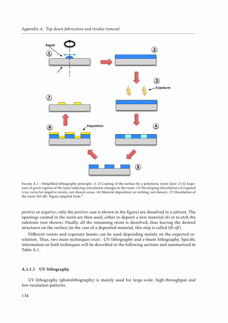
Appendix A. Top-down fabrication and residue removal
Figure A.1 – Simplified lithography principle. (1-2) Coating of the surface by a polymeric resist layer. (3-4) Expo-sure of given regions of the layer inducing reticulation changes in the resist. (5) Developing (dissolution) of exposed(vice-versa for negative resists, not shown) areas. (6) Material deposition (or etching, not shown). (7) Dissolution ofthe resist (lif-off). Figure adapted from.5
positive or negative ; only the positive case is shown in the figure) are dissolved in a solvent. Theopenings created in the resist are then used, either to deposit a new material (6) or to etch thesubstrate (not shown). Finally, all the remaining resist is dissolved, thus leaving the desiredstructures on the surface (in the case of a deposited material, this step is called lift-off ).
Different resists and exposure beams can be used depending mainly on the expected re-solution. Thus, two main techniques exist : UV-lithography and e-beam lithography. Specificinformation on both techniques will be described in the following sections and summarized inTable A.1.
A.1.1.2 UV lithography
UV-lithography (photolithography) is mainly used for large-scale, high-throughput andlow-resolution patterns.
134
A.1. State of the art
In this technique, the resist is exposed to a UV-light (λ ≈ 300nm-400nm). In order to exposeonly given regions of the resist it is necessary to use a mask that is opaque to UV light exceptin the regions that are to be exposed. This allows the motif on the mask to be transferred tothe photoresist. The steps following exposure have been described in the previous section (seeFigure A.1).
Photoresists are resin polymers whose solubility in a developer (basic solvent) change whenexposed to light. Photoresist chemistry is still an active research field but most common posi-tive photoresists are based on DiazoNaphthoQuinone (DNQ)/Novolac 17 (eg : AZ-5206©) whe-reas negative photoresists may be epoxy-based (eg : SU-8©). These are usually developed inTetraMethylAmmonium Hydroxide (TMAH) (eg : AZ XXX MIF©).
The main advantage of photolithography is that many microstructures over a large area (se-veral cm2) can be exposed simultaneously. However, resolution is limited by diffraction, so thatphotolithography is mainly employed for typical sizes over 1µm. Nonetheless, recent advancesin photolithography allow for better resolution (smaller size, smaller spacings and better edgecontrol). These advances and current issues, which shall not be discussed in detail here, includethe use of deep and extreme-UV,6 interferometric lithography7 and use of superlenses.8, 9
A.1.1.3 E-beam lithography
Electron-beam lithography is mainly used for small-scale, low-throughput but high-resolutionpatterns.
In this case, the electron beam of a SEM (≈ 10keV-100keV) is used to directly expose, i.e.,write, the wanted shapes on the resist. Thus, unlike photolithography, no mask is needed. Si-milarly to photoresists, electronic resists are resin polymers whose solubility in a developer ischanged when exposed to electric charges, namely electrons. Among them, PMMA and, morerecently, Hydrogen SilsesQuioxane (HSQ) are widely used. TMAH and Methyl isobutyl ketone(MIBK) are common developers in e-beam lithography.
Using an electron beam to expose the resist is an efficient way to beat the resolution ofphotolithography, limited by light diffraction. Thus, e-beam lithography can be used for na-nometric patterns. However, the exposure process is sequential and can take several hoursfor small areas (≤ 1cm2). Recent advances and current issues on e-beam lithography includethe use of ultrahigh contrast10 and Scanning Transmission Electron Microscope or Microscopy(STEM) lithography.11, 12
A.1.1.4 Summary on UV and e-beam lithographies
In the previous paragraphs we have seen the basic concepts of top-down substrate patter-ning using conventional lithography. It is not the purpose of this brief introduction to discusslithography in detail with its many variants. For this matter, the reader can find the appropriatereferences in the literature.11
Table A.1 summarizes the basics of UV and e-beam lithography.
Photolithography Electron-beam lithographyExposition source UV light (≈ 300nm-400nm) Electron beam (2keV13-350keV13)Resist DNQ-Novolac, Epoxy PMMA, HSQDeveloper TMAH TMAH, MIBKMask Yes No
17. Novolac is a photoresist based on phenol-formaldehyde, enriched in phenol.
135
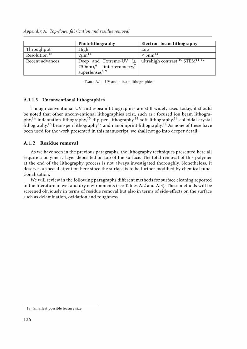
Appendix A. Top-down fabrication and residue removal
Photolithography Electron-beam lithographyThroughput High LowResolution 18 2µm14 ≤ 5nm14
Recent advances Deep and Extreme-UV (≤250nm),6 interferometry,7
superlenses8, 9
ultrahigh contrast,10 STEM11, 12
Table A.1 – UV and e-beam lithographies
A.1.1.5 Unconventional lithographies
Though conventional UV and e-beam lithographies are still widely used today, it shouldbe noted that other unconventional lithographies exist, such as : focused ion beam lithogra-phy,14 indentation lithography,15 dip-pen lithography,14 soft lithography,14 colloidal-crystallithography,16 beam-pen lithography17 and nanoimprint lithography.14 As none of these havebeen used for the work presented in this manuscript, we shall not go into deeper detail.
A.1.2 Residue removal
As we have seen in the previous paragraphs, the lithography techniques presented here allrequire a polymeric layer deposited on top of the surface. The total removal of this polymerat the end of the lithography process is not always investigated thoroughly. Nonetheless, itdeserves a special attention here since the surface is to be further modified by chemical func-tionalization.
We will review in the following paragraphs different methods for surface cleaning reportedin the literature in wet and dry environments (see Tables A.2 and A.3). These methods will bescreened obviously in terms of residue removal but also in terms of side-effects on the surfacesuch as delamination, oxidation and roughness.
18. Smallest possible feature size
136

A.1. State of the artA
.1.2
.1W
etp
roce
sses
Mai
nco
mp
oun
dA
dd
itiv
esP
rin
cip
leA
dva
nta
ges
Dra
wb
ack
sC
omm
ents
Org
anic
solv
ents
:A
ceto
ne18
Eth
anol
,Is
opro
PAno
l(I
PA)18
DC
M18
DiC
hlor
oEth
ane
(DC
E)18
N-M
ethy
lP
yrro
lid
one
(NM
P)18
Non
eO
rgan
icd
isso
luti
onE
ase
ofu
se,
ofte
nin
clu
-d
edin
the
lith
ogra
phy
pro
cess
(eg
:li
ft-o
ff)
Not
enou
ghfo
rto
tal
PMM
Are
mo-
val18
May
beu
sed
wit
hu
ltra
sou
nds
and
/or
heat
ing.
H2SO
4+
H2O
2(P
iran
ha)
Non
eO
xid
atio
nSt
and
ard
pro
-ce
dure
Poss
ible
de-
lam
inat
ion
ofth
infi
lms.
Dan
gero
us.
H2O
319
(ozo
nate
dw
ater
)Su
rfac
tant
:G
lyco
lic
Aci
dE
thox
y-la
te4-
tert
-bu
tylp
heny
lE
ther
(GA
E4E
)19
Cat
ioni
che
xa-
dec
ylTr
ime-
thyl
Am
mo-
niu
mB
rom
ide
(CTA
B)19
Trit
on19
Oxi
dat
ion
+su
rfac
tant
Pro
ven
ef-
fici
ency
ofG
AE
4Eon
SiO
219
Effi
cien
cyp
ro-
ven
onm
odel
pol
ysty
rene
par
ticl
es,
not
onac
tual
lith
ogra
phy
resi
dues
Poss
ibil
ity
tou
sesa
me
surf
acta
ntw
ith
anot
her
solv
ent.
HF
NH
4F
for
Buffe
-re
dO
xid
eE
tch
(BO
E)
Dis
solv
esSi
O2
:Si
O2
+4H
F−→
SiF 4
(g)
+2H
2O
SiO
2+
6HF−→
H2Si
F 6+
2H2O
Ver
yeffi
cien
ton
oxid
es.
Com
mon
lyu
sed
inm
icro
-fa
bric
atio
n.
Rem
oval
ofox
ide
laye
rm
aybe
un-
wan
ted
.D
ange
rou
s.
137

Appendix A. Top-down fabrication and residue removalM
ain
com
pou
nd
Ad
dit
ives
Pri
nci
ple
Ad
van
tage
sD
raw
bac
ks
Com
men
tsB
asic
H2O
20N
H4O
H21
Alk
anol
amin
eK
OH
TM
AH
Bas
icat
tack
Pro
ven
effi-
cien
cyof
KO
Han
dN
H4O
HN
one
edfo
ror
gani
cso
lven
tE
asy
rins
ing
Not
bett
erth
anor
gani
cso
lven
ts
Poss
ible
toad
din
hi-
bito
rsto
avoi
dm
etal
corr
osio
n
Bas
icaq
ueo
us
IPA
22N
H4O
H+
H2O
TM
AH
+H
2O
Bas
icat
tack
+or
gani
cd
isso
luti
onH
2O
lead
sto
dis
soci
a-ti
onof
NH
4O
HO
H−
atta
cks
Si-O
-Si
bond
sbe
twee
nsi
lica
surf
ace
and
Hex
ame-
thyl
dis
ilaz
ane
(HM
DS)
Pro
ven
ef-
fici
ency
onH
MD
Sre
mo-
valf
rom
SiO
2L
ead
sto
low
rugo
sity
TM
AH
effi-
cien
cyno
tp
rove
n
Table
A.2
–W
etp
roce
sses
for
surf
ace
clea
ning
(rem
oval
ofor
gani
cre
sidu
esaf
ter
lith
ogra
phy
).
A.1
.2.2
Dry
pro
cess
es
Mai
nco
mp
oun
dA
dd
itiv
esP
rin
cip
leA
dva
nta
ges
Dra
wb
ack
sC
omm
ents
O2
pla
sma21
Non
eA
shin
gL
ead
sto
oxi-
dat
ion
ofm
e-ta
lsu
rfac
esN
H3
pla
sma23
Non
eO
rgan
ic+
NH
3−→
HC
N+
H2O
UV
nano
seco
ndla
ser21
:A
rF(1
93nm
)X
eCl(
308n
m)
Non
eP
hoto
chem
ical
bond
dis
soci
atio
n:
C=
C,
C-H
,C-N
...
Pro
ven
effi-
cien
cyw
ith
ArF
lase
r
Com
ple
xan
dex
pen
sive
Flu
ence
and
num
ber
ofsh
ots
can
bead
ap-
ted
21
138

A.1. State of the artM
ain
com
pou
nd
Ad
dit
ives
Pri
nci
ple
Ad
van
tage
sD
raw
bac
ks
Com
men
tsN
d3
+Y
ttri
um
Alu
mi-
niu
mG
arne
t,Y
3A
l 5O
12(Y
AG
)(53
2nm
)(v
isib
lela
ser)
24
Non
eT
herm
alab
lati
onH
MD
Sre
mo-
valf
rom
Sino
tp
rove
n
H2O
(scr
ubb
ersp
ray)
21N
one
Mec
hani
cab
rasi
onW
ear
H2O
+ga
z(s
oft
spra
y)21
Non
eM
echa
nic
abra
sion
wit
hd
rop
lets
Wea
r
UV
+O
3N
one
Sup
ercr
itic
alC
O2
21,2
3,25
–27
TM
AH
CO
3+
Met
hOH
Ace
tone
DM
SO19
Uni
que
pro
per
ties
ofd
iffu
sion
and
solv
ata-
tion
Ver
yeffi
cien
tC
omp
lex
and
exp
ensi
ve
Table
A.3
–D
ryp
roce
sses
for
surf
ace
clea
ning
(rem
oval
ofor
gani
cre
sidu
esaf
ter
lith
ogra
phy
).
19.
Dim
ethy
lsu
lfox
ide
139

Appendix A. Top-down fabrication and residue removal
A.1.2.3 Summary on cleaning processes
As evidenced by Tables A.2 and A.3, removal of organic contamination from microfabri-cation processes is an active research topic with many possible answers. Although a relativelystandard cleaning procedure with acetone + alcohol + water is often used, this may not resultin optimum cleaning of the surface, specially when the latter has been previously coated withPMMA.18 Other wet cleaning procedures may be used either in acidic environments (HF, pi-ranha) or basic environments20–22 (ammonia, KOH). The former are known to be very efficientbut may result in delamination or dissolution of the surface, whereas the latter are reportednot to be better than standard organic solvents.
Dry processes can be used instead or in addition to wet cleaning procedures. Among thedifferent options presented in Table A.3, O2 plasma ashing appears as a very good candidateboth for its efficiency and ease of use. However, it must be noted that this procedure may lead tometal oxidation. In the case of gold surfaces, it has been reported that exposure to O2 plasmaleads to Au2O3.28, 29 However, this oxide is unstable at normal temperature and pressure.28
The characteristic dissociation time (oxide half-life) at 20◦C is reported to be 22h and can beaccelerated when rinsing with ethanol29, 30 and/or heating.28
A.2 Materials and methods used during this work
This section presents the protocols used for the top-down substrate patterning and clea-ning. It must be noted that some of these processes were conducted partly or exclusively byothers as specified below :
– Processes exclusively conducted by myself :– Gold evaporation (plain substrate).– Cleaning processes.
– Processes done partly by others :– Photolithography with subsequent gold deposition and lift-off, when not done by my-
self was done by Bertrand Vilquin or Pedro Rojo Romeo at INL.– E-beam lithography and subsequent gold evaporation and lift-off was mostly done by
Pedro Rojo Romeo or Céline Chevalier at INL.
– Processes exclusively done by others :– Silica sputtering, when needed, was carried out by Bertrand Vilquin or Pedro Rojo
Romeo at INL.– Institut d’Électronique Fondamentale (IEF) partners also provided “macro-patterned”
(see Fig. 1.17) gold on glass surfaces.
A.2.1 Lithography
A.2.1.1 Photolithography
The protocol used for photolithography was the following :
1. Spin-coat the HMDS primer followed by AZ 5214 (negative) resist at 5500 rpm for 30s.
140
A.2. Materials and methods used during this work
2. Bake at 110◦C for 1min.
3. Expose to UV through mask for 4s.
4. Bake at 120◦C from 2min.
5. Expose whole sample (flood exposure) to UV for 20s.
6. Develop in TMAH (Metal-Ion Free (MIF) 726) for 1min under constant agitation.
7. Stop development by soaking in ultrapure water.
A.2.1.2 E-beam lithography
The protocol used for e-beam lithography was the following :
1. Spin-coat Methyl methacrylate (MMA) at 3000 rpm
2. Bake at 150◦C for 1,30min.
3. Spin-coat PMMA at 2000 rpm
4. Bake at 180◦C for 1,30min.
5. Expose to e-beam.
6. Develop in MIBK-IPA.
7. Rinse with DCM.
A.2.2 Silica sputtering
For the investigation of silanization and orthogonal functionalizations the substrate was ei-ther : (a) a glass microscope slide, (b) a silicon wafer with a 2µm layer of SiO2 (commercial), (c)a silicon wafer onto which silica was deposited by Bertrand Vilquin at INL or (d) a glass slidecovered by a first layer of gold onto which silica was further deposited by Bernard Bartenlianand co-workers at IEF.
A.2.3 Gold e-beam evaporation
Gold e-beam evaporation on different samples was conducted at INL (either by myself orPedro Rojo Romeo) and IEF (by Bernard Bartenlian and co-workers).
Protocol at INL :
1. Introduce sample in evaporation chamber and pump to a pressure of 1.5 10−6 Torr (tem-perature set at 27K).
2. Switch on the cooling system.
3. Deposition of chromium adhesion layer
(a) Set voltage to 6kV.
(b) Increase current until the deposition rate, monitored by a QCM, reaches ca. 1Å/s (acache is “hiding” the substrate so far so that no deposition occurs on it)
(c) Remove cache and wait until the deposited layer reaches 2-3nm thickness.
(d) Place cache back, decrease current slowly to 0, switch off voltage and wait for thesocket containing the chromium to cool down.
141
Appendix A. Top-down fabrication and residue removal
(e) Change socket to the one containing the gold.
4. Deposition of gold layer
(a) Set voltage to 6kV.
(b) Increase current until the deposition rate, monitored by a QCM, reaches ca. 2Å/s (acache is “hiding” the substrate so far so that no deposition occurs on it)
(c) Remove cache and wait until the deposited layer reaches 45-50nm thickness.
(d) Place cache back, decrease current slowly to 0, switch off voltage and wait for thesocket to cool down.
This process was conducted in a Leybold© e-beam evaporator.
A.2.4 Substrate cleaning
A.2.4.1 Organic solvents
When cleaned only with organic solvents (typically when no resist residues from lithogra-phy were expected) samples were cleaned with the following procedure :
1. Immerse in acetone under sonication for ca. 10min
2. Immerse in ethanol or isopropanol for ca. 5min
3. Immerse in ultrapure water for ca. 5min
4. Dry with nitrogen flow
Alternatively other organic solvents were used such as DCM and heating was also appliedthough this procedures were quickly abandoned in favor of a simpler and more efficient O2plasma, as is detailed in section 3.1.1.
A.2.4.2 O2 Plasma
Oxygen plasma was found to be the most efficient, thus most used cleaning process. Sampleswere cleaned by O2 plasma with the following parameters :
– Applied (forward) power = 350W (typical reflected power was 10W)– Oxygen flow = 400 sccm– Pressure = 90Pa– Time = 5minThis was conducted in an Anatech© chamber where only oxygen and nitrogen are intro-
duced. When this process was conducted in an etching chamber with input lines of differentfluorinated gases (SF6, CHF3) fluor contamination was detected afterwards by XPS analysis.
142
Appendix B
DLVO and colloid stabilization
NB : The following paragraphs are adapted from our previous publication.31
Before examining the means for globally placing individual particles on pre-defined re-gions of a substrate, we must ensure that these particles are stabilized, ie : not aggregated toone another or to the walls of the container. Different forces control the particle/particle (orparticle/wall) interaction. These can be summarized in what is called Derjaguin, Landau, Ver-wey, Overbeek (DLVO) theory. In its most basic form, DLVO theory deals with two interactionforces : Van der Waals (attractive) and electric double-layer effects (repulsive)32, 33.
B.1 Van der Waals attraction
Van der Waals forces, and more precisely London dispersion forces, are attractive forcesarising from the spontaneous polarization of molecules. This polarization effect is enhancedwhen dealing with nano and microparticles. Indeed, the Van der Waals potential energy isproportional to the inverse sixth power of the distance (∝ D−6) when considering two atomsbut the energy per unit area is proportional to the inverse of the distance (∝ D−1) for colloidalparticles34 :
Usphere/sphere = − A6πD
× R1R2
R1 +R2
R1 and R2 being the radii of the spheres, D the distance between them and A the so-calledHamaker constant which depends on the materials.
The derived attractive force will lead the particles to aggregate to each other and to thewalls. Therefore one needs repulsive forces to separate (stabilize) the colloidal dispersion. Themain repulsive force in colloidal solutions is linked to surface charge, through what is calledthe electric double layer.
B.2 Electric double layer repulsion
Surfaces can be charged in polar and non-polar solvents35 by different phenomena thatwill not be discussed here. This surface charge induces an electrostatic potential that decaysexponentially when moving away from the surface, due to the existence of a double counter-ionlayer : a first layer of strongly grafted counter-ions (Stern layer) and a second “diffuse” layerwith a majority of counter-ions (Gouy-Chapman layer).
143
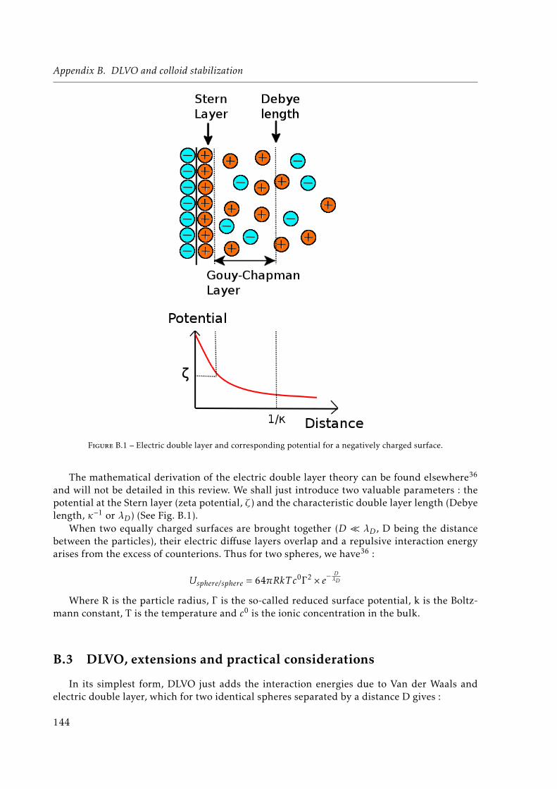
Appendix B. DLVO and colloid stabilization
Figure B.1 – Electric double layer and corresponding potential for a negatively charged surface.
The mathematical derivation of the electric double layer theory can be found elsewhere36
and will not be detailed in this review. We shall just introduce two valuable parameters : thepotential at the Stern layer (zeta potential, ζ) and the characteristic double layer length (Debyelength, κ−1 or λD ) (See Fig. B.1).
When two equally charged surfaces are brought together (D � λD , D being the distancebetween the particles), their electric diffuse layers overlap and a repulsive interaction energyarises from the excess of counterions. Thus for two spheres, we have36 :
Usphere/sphere = 64πRkT c0Γ 2 × e− DλD
Where R is the particle radius, Γ is the so-called reduced surface potential, k is the Boltz-mann constant, T is the temperature and c0 is the ionic concentration in the bulk.
B.3 DLVO, extensions and practical considerations
In its simplest form, DLVO just adds the interaction energies due to Van der Waals andelectric double layer, which for two identical spheres separated by a distance D gives :
144
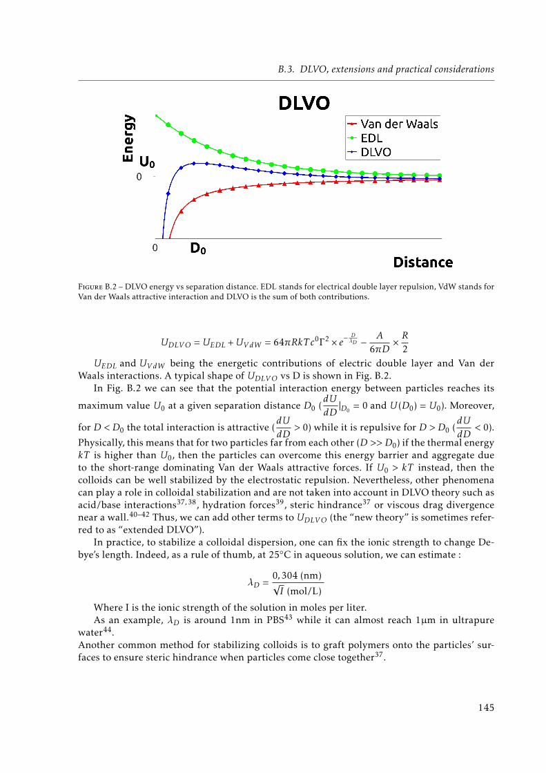
B.3. DLVO, extensions and practical considerations
Figure B.2 – DLVO energy vs separation distance. EDL stands for electrical double layer repulsion, VdW stands forVan der Waals attractive interaction and DLVO is the sum of both contributions.
UDLVO =UEDL +UV dW = 64πRkT c0Γ 2 × e− DλD − A
6πD× R
2UEDL and UV dW being the energetic contributions of electric double layer and Van der
Waals interactions. A typical shape of UDLVO vs D is shown in Fig. B.2.In Fig. B.2 we can see that the potential interaction energy between particles reaches its
maximum value U0 at a given separation distance D0 (dUdD|D0
= 0 and U (D0) = U0). Moreover,
for D < D0 the total interaction is attractive (dUdD
> 0) while it is repulsive for D > D0 (dUdD
< 0).
Physically, this means that for two particles far from each other (D >> D0) if the thermal energykT is higher than U0, then the particles can overcome this energy barrier and aggregate dueto the short-range dominating Van der Waals attractive forces. If U0 > kT instead, then thecolloids can be well stabilized by the electrostatic repulsion. Nevertheless, other phenomenacan play a role in colloidal stabilization and are not taken into account in DLVO theory such asacid/base interactions37, 38, hydration forces39, steric hindrance37 or viscous drag divergencenear a wall.40–42 Thus, we can add other terms to UDLVO (the “new theory” is sometimes refer-red to as “extended DLVO”).
In practice, to stabilize a colloidal dispersion, one can fix the ionic strength to change De-bye’s length. Indeed, as a rule of thumb, at 25◦C in aqueous solution, we can estimate :
λD =0,304 (nm)√I (mol/L)
Where I is the ionic strength of the solution in moles per liter.As an example, λD is around 1nm in PBS43 while it can almost reach 1µm in ultrapure
water44.Another common method for stabilizing colloids is to graft polymers onto the particles’ sur-faces to ensure steric hindrance when particles come close together37.
145

Appendix B. DLVO and colloid stabilization
146
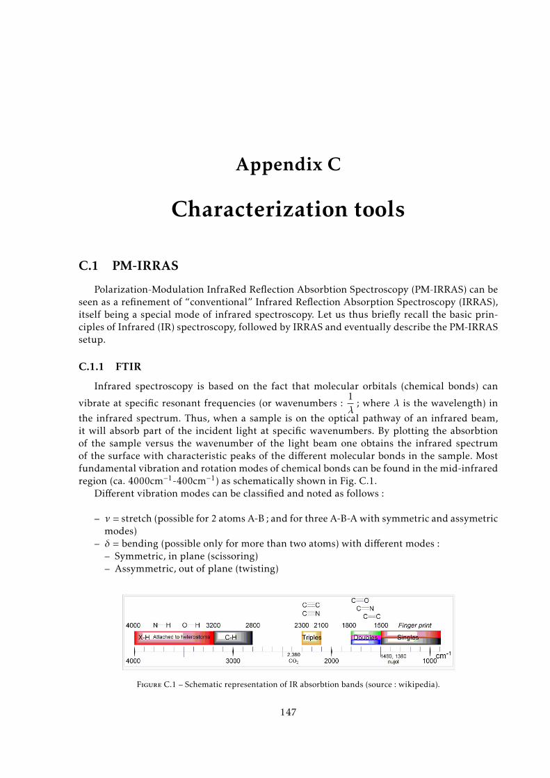
Appendix C
Characterization tools
C.1 PM-IRRAS
Polarization-Modulation InfraRed Reflection Absorbtion Spectroscopy (PM-IRRAS) can beseen as a refinement of “conventional” Infrared Reflection Absorption Spectroscopy (IRRAS),itself being a special mode of infrared spectroscopy. Let us thus briefly recall the basic prin-ciples of Infrared (IR) spectroscopy, followed by IRRAS and eventually describe the PM-IRRASsetup.
C.1.1 FTIR
Infrared spectroscopy is based on the fact that molecular orbitals (chemical bonds) can
vibrate at specific resonant frequencies (or wavenumbers :1λ
; where λ is the wavelength) in
the infrared spectrum. Thus, when a sample is on the optical pathway of an infrared beam,it will absorb part of the incident light at specific wavenumbers. By plotting the absorbtionof the sample versus the wavenumber of the light beam one obtains the infrared spectrumof the surface with characteristic peaks of the different molecular bonds in the sample. Mostfundamental vibration and rotation modes of chemical bonds can be found in the mid-infraredregion (ca. 4000cm−1-400cm−1) as schematically shown in Fig. C.1.
Different vibration modes can be classified and noted as follows :
– ν = stretch (possible for 2 atoms A-B ; and for three A-B-A with symmetric and assymetricmodes)
– δ = bending (possible only for more than two atoms) with different modes :– Symmetric, in plane (scissoring)– Assymmetric, out of plane (twisting)
Figure C.1 – Schematic representation of IR absorbtion bands (source : wikipedia).
147
Appendix C. Characterization tools
– Assymetric, in plane (rocking)– Symetric, out of plane (wagging)
– Fermi resonance (mixing modes) can occur, shifting some peaks or creating doubletsfrom one mode.
In order to probe the absorbtion of a sample at different wavenumbers, it is possible to shinethe sample with a changing monochromatic light beam (through a dispersive spectrometer)thus probing one by one every wavenumber. Dispersive spectrometers are however rarely usedanymore for infrared characterization.
Instead, most infrared spectrometers are based on Fourier-Transform Infrared Spectrosocpy(FTIR). Without going into too much detail about FTIR itself, let us say that in this configura-tion, a “white” light containing the whole spectrum is used. Before reaching the sample, thelight beam is split through a Michelson interferometer which induces a retardation on one ofthe two “halves” of the beam, creating thus constructive and destructive interferences on thebeam that reaches the sample. Thus, the raw data obtained by the detector is an interferogram,that is, the intensity as a function of the retardation. This interferogram is later translated intoa spectrum by a Fourier Transformation, hence the name of the technique.
The spectral resolution is dependent on the amplitude of the moving mirror in the Michel-son Interferometer.
C.1.2 IRRAS
IRRAS is specially suited to probe the chemistry of a highly reflective (specially metallic)surface. In an IRRAS set-up, the infrared light beam is specularly reflected at a grazing in-cidence onto the metallic surface to be probed. At the surface, only the p-polarized light isnon-equal to zero, so that only dipoles having a component perpendicular to the surface canabsorb light. However, as far from the surface the light is not polarized, isotropic absorptionsdue to the environment occur and alter the spectrum (requiring thus the acquisition of a back-ground spectrum prior to probing the sample). This remark is the basis for the PM-IRRASimplementation.
C.1.3 PM-IRRAS
C.1.3.1 PM-IRRAS principle, in short
In a PM-IRRAS setup, the incident beam is polarized prior to reaching the surface. Its po-larization is switched from p to s at a high frequency by a PhotoElastic Modulator (PEM).Simply put, this allows the acquisition of two different signals simultaneously : the sum (R(p)+ R(s)) and difference (|R(p)-R(s)|) reflectivities. By taking the ratio of these two signals :|Rp −Rs|Rp +Rs
=∆RR
one obtains a spectrum of the surface without the contribution of isotropic
absorptions from the environment, having thus a better surface-sensitivity without the need ofacquiring a background spectrum.
148
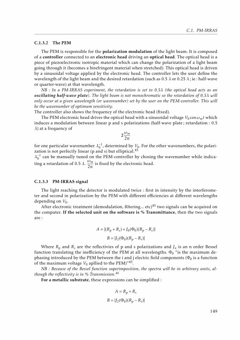
C.1. PM-IRRAS
C.1.3.2 The PEM
The PEM is responsible for the polarization modulation of the light beam. It is composedof a controller connected to an electronic head driving an optical head. The optical head is apiece of piezoelectronic isotropic material which can change the polarization of a light beamgoing through it (becomes a birefringent material when stretched). This optical head is drivenby a sinusoidal voltage applied by the electronic head. The controller lets the user define thewavelength of the light beam and the desired retardation (such as 0.5 λ or 0.25 λ ; ie : half-waveor quarter-wave) at that wavelength.
NB : In a PM-IRRAS experiment, the retardation is set to 0.5λ (the optical head acts as anoscillating half-wave plate). The light beam is not monochromatic so the retardation of 0.5λ willonly occur at a given wavelength (or wavenumber) set by the user on the PEM-controller. This willbe the wavenumber of optimum sensitivity.The controller also shows the frequency of the electronic head (fixed).
The PEM electronic head drives the optical head with a sinusoidal voltage V0 cosωmt whichinduces a modulation between linear p and s polarizations (half-wave plate ; retardation : 0.5λ) at a frequency of
2ωm2π
for one particular wavenumber λ−10 , determined by V0. For the other wavenumbers, the polari-
zation is not perfectly linear (p and s) but elliptical.45
λ−10 can be manually tuned on the PEM-controller by chosing the wavenumber while indica-
ting a retardation of 0.5 λ.ωm2π
is fixed by the electronic head.
C.1.3.3 PM-IRRAS signal
The light reaching the detector is modulated twice : first in intensity by the interferome-ter and second in polarization by the PEM with different efficiencies at different wavelengthsdepending on V0.
After electronic treatment (demodulation, filtering... etc)45 two signals can be acquired onthe computer. If the selected unit on the software is % Transmittance, then the two signalsare :
A = |(Rp +Rs) + J0(Φ0)(Rp −Rs)|B = |J2(Φ0)(Rp −Rs)|
Where Rp and Rs are the reflectivies of p and s polarizations and Jn is an n order Besselfunction translating the inefficiency of the PEM at all wavelengths. Φ0 “is the maximum de-phasing introduced by the PEM between the i and j electric field components (Φ0 is a functionof the maximum voltage V0 apllied to the PEM)”45.
NB : Because of the Bessel function superimposition, the spectra will be in arbitrary units, al-though the reflectivity is in % Transmission.46
For a metallic substrate, these expressions can be simplified :
A = Rp +Rs
B = |J2(Φ0)(Rp −Rs)|
149
Appendix C. Characterization tools
The PM-IRRAS signal can be obtained by ratioing both :
SPMIRRAS =BA
= |J2(Φ0)| |Rp −Rs|Rp +Rs
= |J2(Φ0)|∆RR
NB : For simplicity we have omitted from the equations the electronic gains that can be applied tochannels A and B, as well as the possible different responses of the optical elements (PEM, detector...etc) for p and s polarized light.45
C.1.3.4 Baseline correction and units
In order to obtain the final spectrum∆RR
one needs to normalize the obtained spectrum to
remove the J2(Φ0) contribution. This can be done by different methods :
– A manual baseline correction dividing the spectrum by a spline function46 fitted tothe regions of the spectrum where no peak is expected is often performed.47 This correc-tion gives the correct relative intensities of the peaks (whereas substracting the baselinedoes not).46 However this leads to arbitrary units on the Y-axis and the results are user-dependant.
– A “background” spectrum with a bare substrate can be collected for proper normaliza-tion. However, this requires to have a good reference sample (identical to the test samplewithout the organic layer of interest). Furthermore, it takes away one of the main inter-ests of the PM-IRRAS technique versus conventional IRRAS.
– A mathematically modelled Bessel function can be used. However, the superimposed
function on the experimental∆RR
spectrum may not exactly correspond to a Bessel func-
tion, as it may include experimental biases such as an absorbing layer onto a mirror orimperfect behaviour of the PEM (eg : residual birefringence).45
It is possible to convert the data to absorbance units which enables the comparison of theabsolute intensities of the peaks. However, this is not straightforward.46
C.2 XPS
X-ray Photoelectron Spectroscopy (XPS) is a method that probes the energy of electronspresent in atoms on a surface (ca. 10nm depth). In an XPS experiment, the sample surfaceis exposed to photons in the X-ray range (typical incident energy of photons of 1486.6eV foran aluminium source -AlKα radiation-). These photons interact with core-level electrons thatare thus expelled from the surface with a given kinetic energy that depends on their bindingenergy. A simple energy equality can be written for an elastic collision : |Einput | = |Eoutput | =|Ebinding |+|Ekinetic|. This translates the fact that the energy of the incoming photons is convertedfirst to overcome the binding energy of the electron (ie : bringing the electron to the vacuum
150
C.3. ToF-SIMS
level, in other words ionisation energy of the atom) and the remaining energy is translatedinto kinetic energy of the expelled electron. |Einput | is known and fixed by the source (eg :1486.6eV), |Ekinetic| is measured, so that the binding energy can be simply deduced |Ebinding | =|Einput | − |Ekinetic|.
The XPS analyzer counts the number of electrons (per unit time) reaching the detector witha given kinetic energy (translated into binding energy with the aforementioned relation). Thusa typical XPS spectrum shows an intensity (in “counts per second”) versus binding energywith peaks associated to the energy of electrons in atoms present at the surface. Obviously,only electrons whose binding energy is inferior to the energy of the input X-ray photons can bedetected.
Most importantly, XPS is sensitive to the so-called “chemical shift”. This refers to the factthat electrons at the same quantic state (same orbital) of the same element (eg : C1s orbital of acarbon atom) have slightly different binding energies depending on the chemical environmentof the given atom. This means that a carbon atom participating in a carboxylic acid chemicalgroup O=C-OH has a different XPS spectrum (C1s peak around 289.0eV) than a carbon atomin an alkyl chain CH2-CH2-CH2 (C1s peak around 285.0eV). Thus, XPS which is sometimesreferred to as ESCA (Electron Spectroscopy for Chemical Analysis) is not only an elementalanalysis method but also a chemical one.
C.3 ToF-SIMS
Time-of-Flight Secondary Ion Mass Spectroscopy (ToF-SIMS) is another surface sensitive(typically around 1-2nm depth) analysis method. ToF-SIMS is based on the detection of ionizedmolecular fragments of the molecules present at the surface sample.
A source is used to bombard the sample with a -primary- ion beam (eg : ionized goldclusters or fullerenes), thus liberating ionized fragments of the present molecules. These -secondary- ions are then accelerated with a constant voltage onto a time-of-flight mass spectro-meter that separates the different species according to their mass-to-charge ratio (m/z) whichcan be determined by computing the “time of flight”, that is the time between the generationof the secondary ion and its reaching the detector. Indeed, by equating the potential energyinduced by the fixed voltage Eelectric = zV where z is the charge and V is the voltage, to the
kinetic energy of the ion Ekinetic =mv2
2, where m and v are the mass and velocity of the secon-
dary ion, it can easily be determined that t = α√m/z, where t is the time of flight and α is a
proportionality constant that can be determined with well known ion species response (usuallyhydrocarbons). This technique requires that the ions have a ballistic trajectory, without colli-sion with other species. In other words the mean free path of the ions should be large comparedto the distance between the sample and the detector. Thus, it is required to operate in vacuum(ca. 10Pa).
Obviously, depending on the polarization set between the sample and analyzer only posi-tive or negative ions can be detected simultaneously.
C.4 Contact angle goniometry
Contact angle goniometry is based on the measure of the angle θC formed by a liquid ontoa solid surface in contact with a gas environment (see Fig. C.2).
151
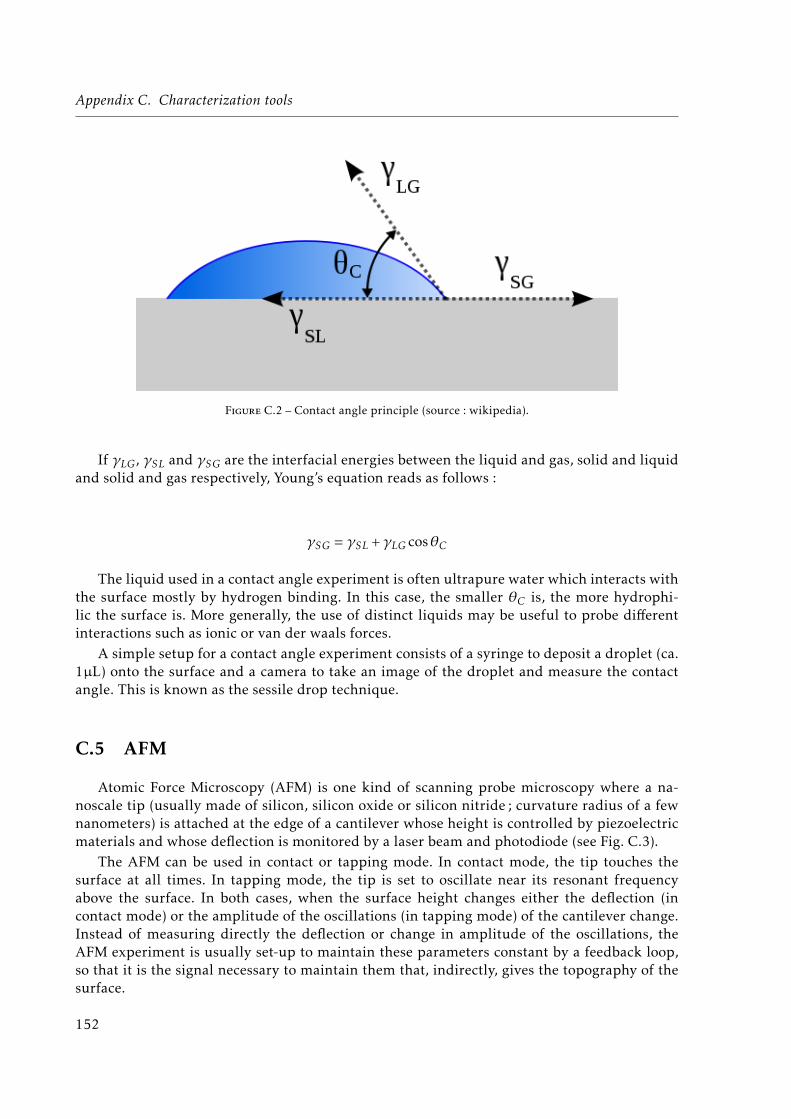
Appendix C. Characterization tools
Figure C.2 – Contact angle principle (source : wikipedia).
If γLG, γSL and γSG are the interfacial energies between the liquid and gas, solid and liquidand solid and gas respectively, Young’s equation reads as follows :
γSG = γSL +γLG cosθC
The liquid used in a contact angle experiment is often ultrapure water which interacts withthe surface mostly by hydrogen binding. In this case, the smaller θC is, the more hydrophi-lic the surface is. More generally, the use of distinct liquids may be useful to probe differentinteractions such as ionic or van der waals forces.
A simple setup for a contact angle experiment consists of a syringe to deposit a droplet (ca.1µL) onto the surface and a camera to take an image of the droplet and measure the contactangle. This is known as the sessile drop technique.
C.5 AFM
Atomic Force Microscopy (AFM) is one kind of scanning probe microscopy where a na-noscale tip (usually made of silicon, silicon oxide or silicon nitride ; curvature radius of a fewnanometers) is attached at the edge of a cantilever whose height is controlled by piezoelectricmaterials and whose deflection is monitored by a laser beam and photodiode (see Fig. C.3).
The AFM can be used in contact or tapping mode. In contact mode, the tip touches thesurface at all times. In tapping mode, the tip is set to oscillate near its resonant frequencyabove the surface. In both cases, when the surface height changes either the deflection (incontact mode) or the amplitude of the oscillations (in tapping mode) of the cantilever change.Instead of measuring directly the deflection or change in amplitude of the oscillations, theAFM experiment is usually set-up to maintain these parameters constant by a feedback loop,so that it is the signal necessary to maintain them that, indirectly, gives the topography of thesurface.
152
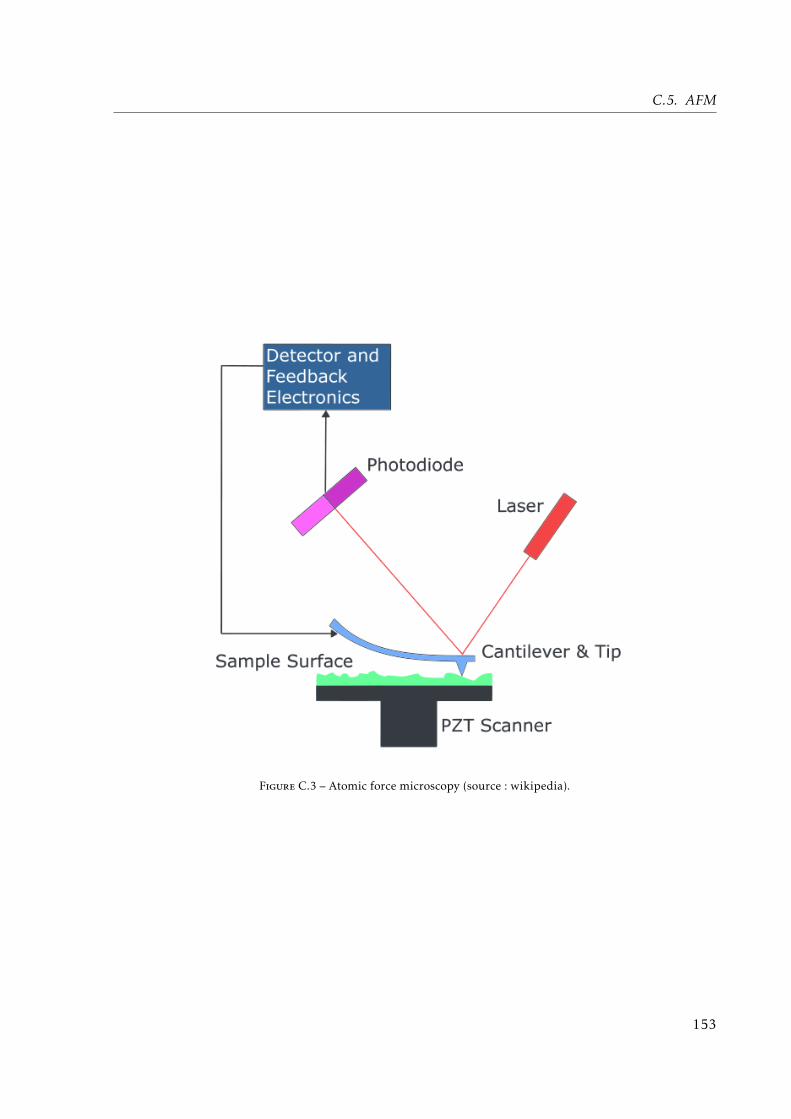
C.5. AFM
Figure C.3 – Atomic force microscopy (source : wikipedia).
153
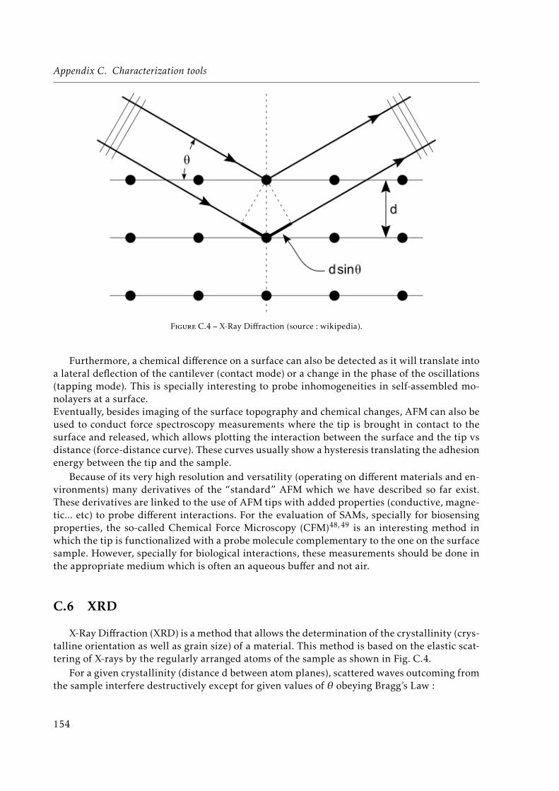
Appendix C. Characterization tools
Figure C.4 – X-Ray Diffraction (source : wikipedia).
Furthermore, a chemical difference on a surface can also be detected as it will translate intoa lateral deflection of the cantilever (contact mode) or a change in the phase of the oscillations(tapping mode). This is specially interesting to probe inhomogeneities in self-assembled mo-nolayers at a surface.Eventually, besides imaging of the surface topography and chemical changes, AFM can also beused to conduct force spectroscopy measurements where the tip is brought in contact to thesurface and released, which allows plotting the interaction between the surface and the tip vsdistance (force-distance curve). These curves usually show a hysteresis translating the adhesionenergy between the tip and the sample.
Because of its very high resolution and versatility (operating on different materials and en-vironments) many derivatives of the “standard” AFM which we have described so far exist.These derivatives are linked to the use of AFM tips with added properties (conductive, magne-tic... etc) to probe different interactions. For the evaluation of SAMs, specially for biosensingproperties, the so-called Chemical Force Microscopy (CFM)48, 49 is an interesting method inwhich the tip is functionalized with a probe molecule complementary to the one on the surfacesample. However, specially for biological interactions, these measurements should be done inthe appropriate medium which is often an aqueous buffer and not air.
C.6 XRD
X-Ray Diffraction (XRD) is a method that allows the determination of the crystallinity (crys-talline orientation as well as grain size) of a material. This method is based on the elastic scat-tering of X-rays by the regularly arranged atoms of the sample as shown in Fig. C.4.
For a given crystallinity (distance d between atom planes), scattered waves outcoming fromthe sample interfere destructively except for given values of θ obeying Bragg’s Law :
154
C.7. SEM
2d sinθ = nλ
where n is an integer and λ is the wavelength of the X-rays.Thus, in an XRD experiment θ is varied and the intensity of the scattered X-ray beam
is measured at each angle. The obtained peaks relate to the different crystalline orientations(computed from the spacings d between atom planes) of the sample.
Moreover, the average grain size δ for a given orientation can be deduced from the corres-ponding diffraction peak with Scherrer’s formula :
δ =Kλ
β cosθ
where K is shape factor parameter (usually equal to 0.9) and β is the full width at halfmaximum of the diffraction peak.
C.7 SEM
In scanning electron microscopy, an electron beam is focused on the sample. This beam“scans” the surface generating secondary electrons among others. These can be driven to adetector which is sensitive to the amount of electrons reaching it. Thus, an intensity can beobtained for each “point” on the surface. The Scanning Electron Microscopy (SEM) image re-presents thus the mapping of this intensity as the input beam scans the sample.Contrast in an SEM image translates a difference in topography and/or material (elements withhigher atomic number give more backscattered electrons, thus a brighter signal).
155

Appendix C. Characterization tools
156
Appendix D
All the things that did not work (wellenough)
This appendix deals briefly with a number of experiments, ideas or side-projects that un-fortunately did not bring significant results to be presented in the core of the manuscript. The“failed” experiments are quickly described and different personal hypothesis are evoked he-reafter. No data is presented to keep this appendix as light as possible.
D.1 Gold functionalization
Gold functionalization is probably the most important part of this PhD. Though functio-nalization of plain and micropatterned substrates has been demonstrated by PM-IRRAS, XPSand ToF-SIMS and functionalization of nanopatterned substrates by colloid trapping (indirectcharacterization), some issues concerning the functionalization could not be clearly elucidated.
D.1.1 Where is the sulfur ?
The XPS spectra of thiolated gold surfaces should reveal the presence of sulfur with a peakat ca. 162 eV (S2p). Furthermore, different contributions could be expected translating thedegree of bonding of the thiols on the gold surface.50 Unfortunately, we were not able to detectthe sulfur contribution despite the co-addition of several tens of scans of the S2p region. Wecan only conclude that under our experimental conditions, the XPS we used is not sensitiveenough to detect the (relatively low) amount of sulfur present on the surface.
D.1.2 Mixed-SAMs
The topic of mixed-SAMs would deserve a full review paper with several pages, extensivereferences and detailed discussions. We will do no such thing here. A brief summary of the lite-rature reports on this topic can be found in paragraph 1.2.1.1.4. To put it simply, in the field ofbiosensors, many papers claim that mixed-SAMs (including thiols with an “active” headgrouplike biotin and thiols with a “diluting” headgroup like alcohol) are better at capturing a targetmolecule (e.g., streptavidin) than monofuctional SAMs (e.g., only biotinylated thiols). I couldnever confirm this hypothesis.
157

Appendix D. All the things that did not work (well enough)
The case of biotinylated thiols is, in my opinion, especially striking. In the words of Hauss-ling et al. : “It was found that the higher the packing density of the biotin labels in the monolayerswas, the less effective was their binding ability.”51 In other words, for a maximum target-bindingefficiency one should dilute the biotinylated thiols with a non-reactive thiol as much as pos-sible, which is coherent with the data presented by Kim et al.52
When I first conducted colloid trapping based on biotin-streptavidin interactions (see sec-tion 3.4.1) I was aware of this literature and thus expected very poor results from a monofunc-tional biotynilated SAM. To my surprise, the 100% biotin-terminated SAM worked at least aswell as a diluted 1/9 biotin/alcohol mixed-SAM.
Furthermore, the “steric hindrance” argument is often evoked in terms like the following :the close-packing of reactive headgroups leads to steric hindrance which reduces the target-binding capabilities of the layer. In my own personal opinion, if this is indeed an entropiceffect, it would be valuable to move from this handwaving argument to a more solid proof. Be-cause protein immobilization seems like a very complex matter, experimental measurementson the amount of immobilized proteins may not be the best suited method to address this fun-damental issue on SAMs. Maybe statistical mechanics and/or numeric simulations can informus better on what “steric hindrance” really is or is not in this case.
D.1.3 Gold oxide silanization
We have seen (section 3.1.1) that oxygen plasma on gold surfaces leads to the formation ofgold oxide and oxides can in principle be silanized. I have tried building a SAM of PEG-silaneon oxidized gold but XPS revealed the absence of the PEG at the end of the process. This wasa “one shot” test which I had no time to investigate further. If such a silanization of gold oxideis possible it could be very interesting from a material science point of view, especially if itcould contribute to the stabilization of this oxide layer. To investigate this, it would certainlybe interesting to better characterize the oxide layer, especially to know the amount of Au-OHsurface groups (if any). It would also be interesting to find an environment which stabilizes theoxide during the silanization.
D.2 Colloid trapping
D.2.1 Covalent coupling
I presented colloid trapping based on bio-affinity and electrostatic interactions (section3.4.1). In all honesty, I did not think that electrostatic binding would resist washing steps and Iexpected to use the electrostatic-based samples as a sort of “control” or “reference” to evaluatecovalent coupling (carboxylatex beads being previously activated into NHS-ester). However,when conducting the NHS-activation on the bead solution the colloidal particles aggregated.This is not surprising since the colloids are stabilized by their negative charge, COO−. Whatthis means is that NHS-activation of carboxylatex has to be undertaken with extra care (asopposed to activation of a COOH SAM on a flat macroscopic surface). Because electrostaticcoupling worked much better than expected and due to the lack of available time, the covalentcoupling scheme was not studied further.
If covalent trapping of colloids on a surface through amide bonds is to be further investi-gated, it might be a good idea to inverse the chemical headgroups : that is, have a COOH-SAMon the flat surface and NH2-latex. Thus, the NHS activation can be carried on flat surface inde-pendently of the colloid dispersion (avoiding aggregation problems).
158

D.2. Colloid trapping
Eventually, it is not sure that covalent coupling should lead to a stronger binding thanelectrostatic interactions. Indeed though a covalent amide bond is probably stronger than an asingle electrostatic interaction between facing COO− and NH+
3 groups, one should also considerthe total number of bonds that can be created between the bead and the surface. Knowingthe dimensions of the bead and the spacing between adjacent chemical groups, it should bepossible to theoretically compute the overall interaction energy. The idea is that electrostaticbonds are present even between chemical groups that are “far” from each other, while chemicalcoupling can only occur on a few facing headgroups.
D.2.2 Electrostatic trapping as a function of ionic strength
I conducted electrostatic trapping in PBS 10X, PBS 1X and ultrapure water at differenttimes (30min, 1h, 2h, 24h, 72h). The idea behind this was to demonstrate the effect of theionic strength (i.e., Debye length) on the electrostatic trapping efficiency. I expected differenttrapping rates as a function of ionic strength, with aggregation occurring on extreme cases.This would enable to start drawing a diagram to find optimum conditions for trapping (as afunction of ionic strength and time). However, the results (assessed by SEM) did not show avery clear trend in surface coverage. As this was done only once on a single set of samples(again a “one shot” experiment due to lack of time and samples) it was difficult to make anyconclusion on the experiment.
D.2.3 Combination with physical approaches
D.2.3.1 Magnetic
The beads used on the bio-affinity method are magnetic latex. I tried to use the magneticproperties to enhance the trapping (surface coverage) of these beads by attracting them towardsthe sample surface (from the bulk liquid phase) with a macroscopic neodymium magnet. Inthis experiment, the sample patterned surface was placed in the center of a liquid millimetric“cell”, immersed in the bead solution (few millilitres). The magnet was placed below the cell.The idea was not to rely on diffusion alone to make the beads reach the surface. However,the attraction by the magnet was stronger than expected and the beads ended up moving tothe edges of the cell (i.e., far from the sample surface which was placed at the center of thecell) because they were preferentially attracted to the edges of the macroscopic magnet (bordereffect).
If magnetic trapping is desired it must certainly be done in a smarter and less naive waywith patterned micro-magnets for instance.
D.2.3.2 Capillary Force Assembly
In a collaboration with CEA-LITEN we also tried combining the trapping of colloids basedon surface chemistry and capillary force assembly (CFA). The idea was to create a dense colloidmonolayer by CFA (dip-coating) and then wash the surface so that only the beads that were ona trapping region (with a matching surface chemistry) would stay on the surface while theother beads (remaining only by Van der Waals adsorption forces) would be washed away. Thisdid not work. It is unclear if the surface functionalization was really efficient at that time.Furthermore, it is probably not a good idea to rely on building a dense particle layer first andwash away later. Indeed, it would be better to ensure that particles only “stick” to the trappingregions during the CFA (dip-coating).
159
Appendix D. All the things that did not work (well enough)
D.3 Applications beyond trapping
D.3.1 Plasmonics
The title of this PhD explicitly deals with plasmonics (LSPR biosensors). However, we couldunfortunately never demonstrate a plasmonic application. The “nano-antennas” presented insection 3.4.2 were tested in vain for an enhanced Raman signal (SERS). It seems that the geo-metry of these nanostructures (gap size of the dimers especially) does not correspond to thedesired geometry for an enhancement of the electric field, due to poor lithography results.Furthermore the Piranex project for which most of this work was developed aims at develo-ping a combined SERS/LSPR imaging biosensor with nanopatterned gold on silica samples(different from the nano-antennas mentioned above). From a photonic point of view, this hasbeen validated by simulation but not yet with a real sample. We can only hope that when realphotonic-efficient samples do come, the orthogonal chemistry developed in this PhD can beapplied to direct the biomolecules onto the photonic hot-spots and lead to an enhancement ofthe biosensor sensitivity.
D.3.2 Recursive colloidal lithography
Colloidal or nanosphere lithography (NSL) is based on using a dense monolayer of nano-particles on a surface as a mask for nanopatterning. Indeed, if a material is deposited on thissurface and the beads are then “lifted-off”, the material will remain only on the spaces betweenthe beads. My idea was to :
1. Use nanosphere lithography to build nanopatterned gold on silica surfaces (somethingfairly common in the literature).
2. Functionalize this patterned surfaces in order to allow the selective trapping of a secondset of beads only on the gold regions (just as I did with the nanostructures in section3.4.2).
3. Use the selectively-immobilized beads as a mask for a second patterning (e.g., with silver)and lift-off the beads.
Unfortunately, I had this idea at the very end of my PhD with no more than a week to testit. In a sense I could say I tested this with a protocol that was the opposite of “optimized”. Ascould be expected I failed at the very first step (could not build a monolayer of polystyreneparticles on a silica surface by dip coating or spin-coating). Nonetheless I believe that withsome optimization this process can be efficiently carried out.
If it were successful, other than being “fun”, it could be interesting as a way to create multi-material nanopatterning. The “strength” of this process would be that it relies only on self-assembly whereas if you were to do such a multi-material nanopatterning based on other tech-niques like imprint lithography, you would need to have a nanometric lateral resolution tomatch the first and second steps (levels) which I doubt is feasible.
160
References
[1] G. E. Moore. Proceedings of the IEEE, 86,82–85 (1998).
[2] A. Belarouci, T. Benyattou, X. Letartre, and P. Viktorovitch. Optics express, 18,381–94 (2010).
[3] J.-P. Cloarec, Y. Chevolot, E. Laurenceau, M. Phaner-Goutorbe, and E. Souteyrand. ITBM-RBM, 29,105–127 (2008).
[4] Y. Chevolot, C. Bouillon, A. Meyer, J.-P. Cloarec, A. Jochum, J.-p. Praly, J.-J. Vasseur, andE. Souteyrand. Angew. Chem. Int. Ed., 46,2398–2402 (2007).
[5] A. Duval, A. Laisné, D. Pompon, S. Held, A. Bellemain, J. J. Moreau, M. M. Canva, J. Mo-reau, and M. Canva. Optics letters, 34,3634–3636 (2009).
[6] G. O’Sullivan, D. Kilbane, and R. D’Arcy. Journal of Modern Optics, 59,855–872 (2012).
[7] J. Adams, G. Tizazu, S. Janusz, S. R. J. Brueck, G. P. Lopez, and G. J. Leggett. Langmuir,26,13600–13606 (2010).
[8] H. Liu, B. Wang, L. Ke, J. Deng, C. C. Chum, S. L. Teo, L. Shen, S. a. Maier, and J. Teng.Nano letters, 12,1549–54 (2012).
[9] J. Dong, J. Liu, X. Zhao, P. Liu, J. Xie, and Y. Wang. EPL (Europhysics Letters),102,24002 (2013).
[10] L. Y. M. Tobing, L. Tjahjana, and D. H. Zhang. Nanotechnology, 24,075303 (2013).
[11] V. R. Manfrinato, L. Zhang, D. Su, H. Duan, R. G. Hobbs, E. a. Stach, and K. K. Berggren.Nano letters, 13,1555–8 (2013).
[12] C. Vieu, F. Carcenac, A. Pepin, Y. Chen, M. Mejias, A. Lebib, L. Couraud, and H. Launois.Applied Surface Science, 164,111–117 (2000).
[13] V. R. Manfrinato, L. L. Cheong, H. Duan, D. Winston, H. I. Smith, and K. K. Berggren.Microelectronic Engineering, 88,3070–3074 (2011).
[14] A. Pimpin and W. Srituravanich. Engineering Journal, 16,37–56 (2012).
[15] J. Gong, D. J. Lipomi, J. Deng, Z. Nie, X. Chen, N. X. Randall, R. Nair, and G. M. White-sides. Nano Letters, 10,2702–2708 (2010).
[16] J. Zhang, Y. Li, X. Zhang, and B. Yang. Advanced materials, 22,4249–69 (2010).
[17] F. Huo, G. Zheng, X. Liao, and L. R. Giam. Nature nanotechnology, 5 (2010).
[18] D. S. Macintyre, O. Ignatova, S. Thoms, and I. G. Thayne. Journal of Vacuum Science &Technology B : Microelectronics and Nanometer Structures, 27,2597 (2009).
[19] J. Yang, K. Im, and S. Lim. Applied Surface Science, 257,5476–5479 (2011).
[20] J. Petit and J. Moore. Eliminating Solvents in Resist Removal Processes Using Low-CostDetergents. In ASMC (Advanced Semiconductor Manufacturing Conference) Proceedings,pages 301–306 (2010).
161
References
[21] D. Grojo. Mécanismes d’enlèvement de particules par laser impulsionnel : application au net-toyage pour la microélectronique. PhD thesis, Université de la Méditérranée, Aix-MarseilleII (2006).
[22] T. Kamal and D. W. Hess. Journal of Vacuum Science & Technology B : Microelectronics andNanometer Structures, 19,461 (2001).
[23] S. Myneni and D. W. Hess. Journal of The Electrochemical Society, 152,G757 (2005).
[24] H. Horibe, M. Fujita, I. Nishiyama, and A. Yoshikado. Japanese Journal of Applied Physics,44,8673–8675 (2005).
[25] S. Zhang, X.-W. Zhao, H. Xu, R. Zhu, and Z.-Z. Gu. Journal of Colloid and Interface Science,316,168 (2007).
[26] X. Zhang and K. P. Johnston. Chinese Science Bulletin, 52,27–33 (2007).
[27] S. Kim, H. Yuvaraj, Y. Jeong, C. Park, and K. Lim. Microelectronic Engineering, 86,171–175 (2009).
[28] H. Tsai. Surface Science, 537,L447–L450 (2003).
[29] H. Ron, S. Matlis, and I. Rubinstein. Langmuir, 14,1116–1121 (1998).
[30] K. M. Cook and G. S. Ferguson. Chemical communications (Cambridge, England), 47,12550–2 (2011).
[31] F. Palazon, V. Monnier, Y. Chevolot, J.-P. Cloarec, and E. Souteyrand. Journal of ColloidScience and Biotechnology, 2,1–14 (2013).
[32] B. V. Derjaguin and L. Landau. Acta Physicochim. URSS, 14,633–662 (1941).
[33] E. J. W. Verwey and J. T. G. Overbeek. Theory of the Stability of Lyophobic Colloids (1948).
[34] B. Derjaguin. Kolloid-Zeitschrift, 69,155–164 (1934).
[35] C. E. Espinosa, Q. Guo, V. Singh, and S. H. Behrens. Langmuir, 26,16941–16948 (2010).
[36] S. Bhattacharjee, M. Elimelech, and M. Borkovec. Croatica Chemica Acta, 71,5–8 (1998).
[37] C. J. van Oss. Journal of molecular recognition : JMR, 16,177–190 (2003).
[38] J. A. Brant and A. E. Childress. Journal of membrane science, 203,257–273 (2002).
[39] J. Sabín, G. Prieto, J. M. Ruso, R. Hidalgo-Alvarez, and F. Sarmiento. The European physicaljournal. E, Soft matter, 20,401–8 (2006).
[40] A. D. Maude. British Journal of Applied Physics, 293,4–7 (1961).
[41] C. Cottin-Bizonne, A. Steinberger, B. Cross, O. Raccurt, and E. Charlaix. Langmuir,24,1165–1172 (2008).
[42] A. Despeyroux and A. Ambari. Journal of Non-Newtonian Fluid Mechanics, 167-168,38–45 (2012).
[43] E. Stern, R. Wagner, and F. J. Sigworth. Nano Letters, 7,3405–3409 (2007).
[44] E. Thormann, A. C. Simonsen, P. L. Hansen, and O. G. Mouritsen. Langmuir, 24,7278–7284 (2008).
[45] T. Buffeteau, B. Desbat, J. M. Turlet, and C. D. P. Moleculaire. Applied Spectroscopy, 45,380–389 (1991).
[46] B. L. Frey, R. M. Corn, and S. C. Weibel. Handbook of Vibrational Spectroscopy, 2,1042–1056 (2001).
[47] C. Methivier, B. Beccard, and C. M. Pradier. Langmuir, 19,8807–8812 (2003).
162

[48] D. Vezenov, A. Noy, and P. Ashby. Journal of adhesion science and technology, 19,37–41 (2005).
[49] A. Noy. Surface and interface analysis, 38,1429–1441 (2006).
[50] V. Lebec, J. Landoulsi, S. Boujday, C. Poleunis, C.-M. Pradier, and a. Delcorte. The Journalof Physical Chemistry C, 117,11569–11577 (2013).
[51] L. Haussling, H. Ringsdorf, F.-J. Schmitt, and W. Knoll. Langmuir, 7,1837–1840 (1991).
[52] D.-J. Kim and K.-K. Koo. J. Ind. Eng. Chem., 10,920–926 (2004).
163
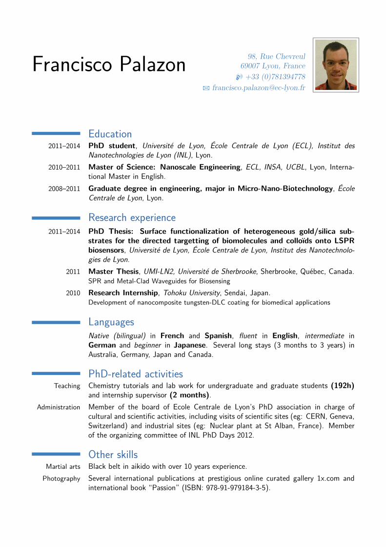
Francisco Palazon 98, Rue Chevreul69007 Lyon, FranceH +33 (0)781394778
Education2011–2014 PhD student, Université de Lyon, École Centrale de Lyon (ECL), Institut des
Nanotechnologies de Lyon (INL), Lyon.2010–2011 Master of Science: Nanoscale Engineering, ECL, INSA, UCBL, Lyon, Interna-
tional Master in English.2008–2011 Graduate degree in engineering, major in Micro-Nano-Biotechnology, École
Centrale de Lyon, Lyon.
Research experience2011–2014 PhD Thesis: Surface functionalization of heterogeneous gold/silica sub-
strates for the directed targetting of biomolecules and colloïds onto LSPRbiosensors, Université de Lyon, École Centrale de Lyon, Institut des Nanotechnolo-gies de Lyon.
2011 Master Thesis, UMI-LN2, Université de Sherbrooke, Sherbrooke, Québec, Canada.SPR and Metal-Clad Waveguides for Biosensing
2010 Research Internship, Tohoku University, Sendai, Japan.Development of nanocomposite tungsten-DLC coating for biomedical applications
LanguagesNative (bilingual) in French and Spanish, fluent in English, intermediate inGerman and beginner in Japanese. Several long stays (3 months to 3 years) inAustralia, Germany, Japan and Canada.
PhD-related activitiesTeaching Chemistry tutorials and lab work for undergraduate and graduate students (192h)
and internship supervisor (2 months).Administration Member of the board of Ecole Centrale de Lyon’s PhD association in charge of
cultural and scientific activities, including visits of scientific sites (eg: CERN, Geneva,Switzerland) and industrial sites (eg: Nuclear plant at St Alban, France). Memberof the organizing committee of INL PhD Days 2012.
Other skillsMartial arts Black belt in aikido with over 10 years experience.Photography Several international publications at prestigious online curated gallery 1x.com and
international book “Passion” (ISBN: 978-91-979184-3-5).
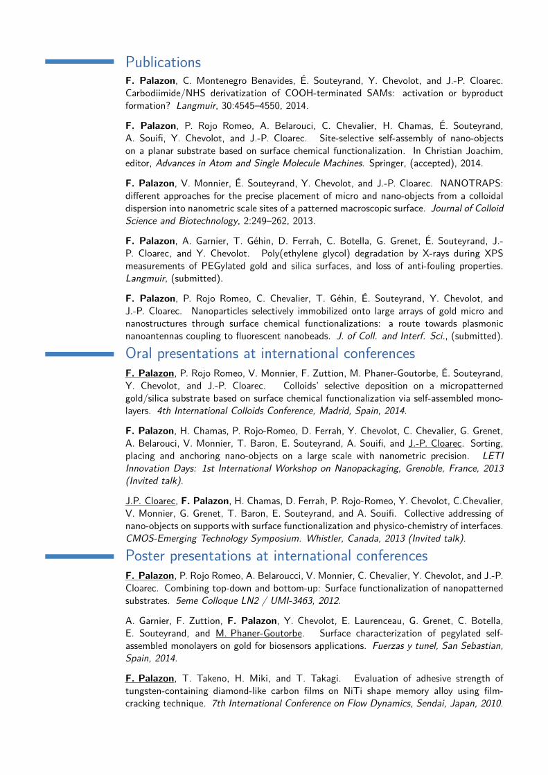
PublicationsF. Palazon, C. Montenegro Benavides, É. Souteyrand, Y. Chevolot, and J.-P. Cloarec.Carbodiimide/NHS derivatization of COOH-terminated SAMs: activation or byproductformation? Langmuir, 30:4545–4550, 2014.
F. Palazon, P. Rojo Romeo, A. Belarouci, C. Chevalier, H. Chamas, É. Souteyrand,A. Souifi, Y. Chevolot, and J.-P. Cloarec. Site-selective self-assembly of nano-objectson a planar substrate based on surface chemical functionalization. In Christian Joachim,editor, Advances in Atom and Single Molecule Machines. Springer, (accepted), 2014.
F. Palazon, V. Monnier, É. Souteyrand, Y. Chevolot, and J.-P. Cloarec. NANOTRAPS:different approaches for the precise placement of micro and nano-objects from a colloidaldispersion into nanometric scale sites of a patterned macroscopic surface. Journal of ColloidScience and Biotechnology, 2:249–262, 2013.
F. Palazon, A. Garnier, T. Géhin, D. Ferrah, C. Botella, G. Grenet, É. Souteyrand, J.-P. Cloarec, and Y. Chevolot. Poly(ethylene glycol) degradation by X-rays during XPSmeasurements of PEGylated gold and silica surfaces, and loss of anti-fouling properties.Langmuir, (submitted).
F. Palazon, P. Rojo Romeo, C. Chevalier, T. Géhin, É. Souteyrand, Y. Chevolot, andJ.-P. Cloarec. Nanoparticles selectively immobilized onto large arrays of gold micro andnanostructures through surface chemical functionalizations: a route towards plasmonicnanoantennas coupling to fluorescent nanobeads. J. of Coll. and Interf. Sci., (submitted).
Oral presentations at international conferencesF. Palazon, P. Rojo Romeo, V. Monnier, F. Zuttion, M. Phaner-Goutorbe, É. Souteyrand,Y. Chevolot, and J.-P. Cloarec. Colloids’ selective deposition on a micropatternedgold/silica substrate based on surface chemical functionalization via self-assembled mono-layers. 4th International Colloids Conference, Madrid, Spain, 2014.
F. Palazon, H. Chamas, P. Rojo-Romeo, D. Ferrah, Y. Chevolot, C. Chevalier, G. Grenet,A. Belarouci, V. Monnier, T. Baron, E. Souteyrand, A. Souifi, and J.-P. Cloarec. Sorting,placing and anchoring nano-objects on a large scale with nanometric precision. LETIInnovation Days: 1st International Workshop on Nanopackaging, Grenoble, France, 2013(Invited talk).
J.P. Cloarec, F. Palazon, H. Chamas, D. Ferrah, P. Rojo-Romeo, Y. Chevolot, C.Chevalier,V. Monnier, G. Grenet, T. Baron, E. Souteyrand, and A. Souifi. Collective addressing ofnano-objects on supports with surface functionalization and physico-chemistry of interfaces.CMOS-Emerging Technology Symposium. Whistler, Canada, 2013 (Invited talk).
Poster presentations at international conferencesF. Palazon, P. Rojo Romeo, A. Belaroucci, V. Monnier, C. Chevalier, Y. Chevolot, and J.-P.Cloarec. Combining top-down and bottom-up: Surface functionalization of nanopatternedsubstrates. 5eme Colloque LN2 / UMI-3463, 2012.
A. Garnier, F. Zuttion, F. Palazon, Y. Chevolot, E. Laurenceau, G. Grenet, C. Botella,E. Souteyrand, and M. Phaner-Goutorbe. Surface characterization of pegylated self-assembled monolayers on gold for biosensors applications. Fuerzas y tunel, San Sebastian,Spain, 2014.
F. Palazon, T. Takeno, H. Miki, and T. Takagi. Evaluation of adhesive strength oftungsten-containing diamond-like carbon films on NiTi shape memory alloy using film-cracking technique. 7th International Conference on Flow Dynamics, Sendai, Japan, 2010.


Summary - Résumé
Orthogonal surface chemical functionalization is an efficient method for the selective trappingof different targets (biomolecules or nano-objects) onto predefined regions of a patterned substrate.This is specially interesting in the field of localized surface plasmon resonance (LSPR) biosensors,where transduction only occurs on metallic nanostructures. The aim is thus to ensure that the targetmolecules can be selectively anchored onto these nanostructres and not adsorbed on the surroun-ding dielectric surface. Thus, we have developped during this PhD different orthogonal functio-nalizations of micro and nanopatterned gold on silica surfaces with thiols and silanes. In regardsto the state of the art in this topic, we have proposed a single-step protocol and demonstrated thegood orthogonality of such functionalizations by extensive surface chemical characterization inclu-ding PM-IRRAS, XPS and ToF-SIMS analysis. Furthermore, these functionalizations have been usedfor the selective anchoring of different latex nanoparticles onto micro and nanopatterns of goldsurrounded by silica, as shown by SEM. At the moment, this methodology is being applied in twodifferent photonic devices where we expect on the one hand a coupling between fluorescent nano-beads and plasmonic nano-antennas and, on the other hand, the increase in sensitivity of an LSPRbiosensor for detecting different biomolecules.
La fonctionnalisation chimique de surfaces hétérogènes (fonctionnalisation orthogonale) est uneméthode efficace pour diriger l’ancrage de diverses cibles (biomolécues ou nano-objets) sur deszones précises prédéfinies sur un substrat. Ceci est particulièrement intéressant dans le domainedes biocapteurs à plasmons localisés (LSPR) où la transduction ne peut se faire que sur des nano-structures métalliques. L’enjeu est alors d’assurer que les molécules à détecter se fixent spécifique-ment sur ces nanostructures et ne s’adsorbent pas sur la surface diélectrique environnante. Dans cebut, nous avons développé dans cette thèse des fonctionnalisations orthogonales de surfaces microet nanostructurées d’or sur silice à l’aide de divers thiols et silanes. Par rapport à l’état de l’art dansce domaine, nous avons notamment proposé un protocole en une seule étape et démontré la bonneorthogonalité de ces fonctionnalisations par différentes méthodes de caractérisation chimique desurface (notamment PM-IRRAS, XPS et ToF-SIMS). De plus, ces fonctionnalisations sélectives ontpermis l’ancrage spécifique de diverses nanoparticules de latex sur des micro et nanostructures d’orentourées de silice, démontré par MEB. Actuellement, cette méthodologie est en cours d’applica-tion dans deux composants photoniques différents où l’on attend d’une part des effets d’exaltationde fluorescence par couplage de nano-antennes et nanobilles marquées et d’autre part un gain ensensibilité d’un biocapteur LSPR pour la détection de différentes biomolécules.