Support for partial run-time reconfiguration of platform FPGAs
18
Support for partial run-time reconfiguration of platform FPGAs q Miguel L. Silva a, * , Joa ˜o Canas Ferreira a,b a Faculdade de Engenharia da Universidade do Porto, Rua Dr. Roberto Frias, s/n, 4200-465 Porto, Portugal b INESC Porto, Rua Dr. Roberto Frias, s/n, 4200-465 Porto, Portugal Received 5 September 2005; received in revised form 6 April 2006; accepted 21 April 2006 Available online 5 July 2006 Abstract Run-time partial reconfiguration of programmable hardware devices can be applied to enhance many applications in high-end embedded systems, particularly those that employ recent platform FPGAs. The effective use of this approach is often hampered by the complexity added to the system development process and by limited tool support. The paper is concerned with several aspects related to the effective exploitation of run-time partial reconfiguration, with particular emphasis on the generation of partial configurations and the run-time utilisation of the reconfigurable resources. The paper presents an approach inspired by the traditional software development: partial configurations are produced by assembling components from a previously created library, thus enabling the embedded application developer to produce the configuration data required for run-time modifications with less effort than is needed with the conventional design flow. A tool that supports this approach is also described. A second set of issues is addressed by a run-time support library that provides facilities for managing the hardware reconfiguration process and the communication with the reconfigured circuits. The use of run-time partial reconfiguration requires a high level of system support. The paper describes one possible approach, presenting a demonstration system developed to support the present work and characterising its performance. In order to clarify the advantages of the approach to run-time reconfiguration discussed in the paper, two small case stud- ies are described, the first on the use of dedicated datapaths for subword operations and the second on two-dimensional pattern-matching for bilevel images. Timing measurements for both cases are included. Ó 2006 Elsevier B.V. All rights reserved. Keywords: Run-time reconfiguration; Partial reconfiguration; Platform FPGA; Bitstream manipulation; Run-time support system 1. Introduction The potential benefits of run-time reconfigura- tion (RTR) of programmable hardware devices have been recognised for some time [1,2]. The importance of this approach has increased with the introduction of platform FPGAs: high-capacity devices with a wide variety of dedicated blocks like 1383-7621/$ - see front matter Ó 2006 Elsevier B.V. All rights reserved. doi:10.1016/j.sysarc.2006.04.004 q This work has been partially funded by the Department of Electrical and Computer Engineering of the Faculty of Engi- neering of the University of Porto (FEUP), under Contract DEEC-ID/05/2003, and by FCT scholarship SFRH/BD/17029/ 2004. * Corresponding author. Tel.: +351 22 508 1502. E-mail addresses: [email protected] (M.L. Silva), [email protected] (J.C. Ferreira). Journal of Systems Architecture 52 (2006) 709–726 www.elsevier.com/locate/sysarc
-
Upload
independent -
Category
Documents
-
view
1 -
download
0
Transcript of Support for partial run-time reconfiguration of platform FPGAs

Journal of Systems Architecture 52 (2006) 709–726
www.elsevier.com/locate/sysarc
Support for partial run-time reconfigurationof platform FPGAs q
Miguel L. Silva a,*, Joao Canas Ferreira a,b
a Faculdade de Engenharia da Universidade do Porto, Rua Dr. Roberto Frias, s/n, 4200-465 Porto, Portugalb INESC Porto, Rua Dr. Roberto Frias, s/n, 4200-465 Porto, Portugal
Received 5 September 2005; received in revised form 6 April 2006; accepted 21 April 2006Available online 5 July 2006
Abstract
Run-time partial reconfiguration of programmable hardware devices can be applied to enhance many applications inhigh-end embedded systems, particularly those that employ recent platform FPGAs. The effective use of this approachis often hampered by the complexity added to the system development process and by limited tool support.
The paper is concerned with several aspects related to the effective exploitation of run-time partial reconfiguration, withparticular emphasis on the generation of partial configurations and the run-time utilisation of the reconfigurable resources.The paper presents an approach inspired by the traditional software development: partial configurations are produced byassembling components from a previously created library, thus enabling the embedded application developer to producethe configuration data required for run-time modifications with less effort than is needed with the conventional design flow.A tool that supports this approach is also described. A second set of issues is addressed by a run-time support library thatprovides facilities for managing the hardware reconfiguration process and the communication with the reconfiguredcircuits.
The use of run-time partial reconfiguration requires a high level of system support. The paper describes one possibleapproach, presenting a demonstration system developed to support the present work and characterising its performance.In order to clarify the advantages of the approach to run-time reconfiguration discussed in the paper, two small case stud-ies are described, the first on the use of dedicated datapaths for subword operations and the second on two-dimensionalpattern-matching for bilevel images. Timing measurements for both cases are included.� 2006 Elsevier B.V. All rights reserved.
Keywords: Run-time reconfiguration; Partial reconfiguration; Platform FPGA; Bitstream manipulation; Run-time support system
1383-7621/$ - see front matter � 2006 Elsevier B.V. All rights reserved
doi:10.1016/j.sysarc.2006.04.004
q This work has been partially funded by the Department ofElectrical and Computer Engineering of the Faculty of Engi-neering of the University of Porto (FEUP), under ContractDEEC-ID/05/2003, and by FCT scholarship SFRH/BD/17029/2004.
* Corresponding author. Tel.: +351 22 508 1502.E-mail addresses: [email protected] (M.L. Silva), [email protected]
(J.C. Ferreira).
1. Introduction
The potential benefits of run-time reconfigura-tion (RTR) of programmable hardware deviceshave been recognised for some time [1,2]. Theimportance of this approach has increased withthe introduction of platform FPGAs: high-capacitydevices with a wide variety of dedicated blocks like
.
710 M.L. Silva, J.C. Ferreira / Journal of Systems Architecture 52 (2006) 709–726
RAMs, multipliers, DLLs and even embedded gen-eral-purpose CPUs. In such an environment, it isnatural that control-intensive sections of an applica-tion are carried out by the CPU, while the reconfig-urable fabric provides hardware support for thedata-intensive sections. This arrangement can betaken a step further for platform FPGAs that sup-port partial reconfiguration of an FPGA regionwithout disturbing the operation of other regions:part of the reconfigurable fabric may be changeddynamically (i.e., at run-time) to accommodate theprecise needs of the application. The end resultmay be a more flexible system with improvedperformance.
Current commercial tool support for dynamicreconfiguration is restricted. The best-supportedscenario involves an application which uses a fewdifferent configurations with substantial commonsections. Available tools produce the differential bit-streams required to take the FPGA from one config-uration to the other. There is typically no supportfor a design flow specific to RTR-based designs.Instead, some slight modifications of regular, non-RTR design flows are provided, whose usefulnessis limited by the fact that such environments aregeared towards complete, fixed designs. For exam-ple, simulation support for RTR-based designs isusually lacking.
From the designer’s perspective, an appropriatedesign flow would allow the independent creationof reusable RTR modules, provide a systematicway of integrating them in different designs (withoutthe need to produce complete designs of all possiblemodule combinations), and support the simulationof all RTR-related behaviour. It should also be pos-sible to impose and check timing constraints on thefinal assembly of RTR modules.
For the creation of efficient RTR-based designs itis important that the FPGA supports partial recon-figuration without disturbing the operation of thecircuits in the unmodified regions. In addition,reconfiguration should be fast, since long configura-tion switching times reduce the number of potentialapplications. This probably implies the desirabilityof fine-grained reconfigurability. It should also bepossible to control the reconfiguration from withinthe device itself, without recourse to an externalcontroller. In addition, a way of efficiently savingand restoring the state of memory elements shouldbe available.
FPGA devices with support for partial RTR arecurrently available from two vendors. Xilinx pro-
vides the Virtex, Virtex-II, Virtex-II Pro and Vir-tex-4 families. Virtex-II Pro and Virtex-4 devicesmay contain embedded microprocessor cores [3].Atmel provides the AT40K and the FPSLIC fami-lies. The latter combines an 8-bit microcontrollerwith an AT40K-based FPGA on the same device[4].
At the highest level, the systems treated in thiswork may be considered to consist of two parts.The fixed part includes the main CPU and all thesupporting modules that remain unchanged duringthe whole execution (for instance, an SRAM con-troller to access off-chip memory, or an I/O periph-eral). Any application-specific accelerators that arenecessary throughout the execution also belong tothe fixed part. All this functionality may be imple-mented by using the resources of the reconfigurablefabric. Even the CPU itself may be implemented inthis way for FPGAs without a dedicated processorblock [5].
The other part of the system includes all thosemodules that are only present temporarily. Themodules time-share a region of the reconfigurablefabric that is reserved for the purpose. (For simplic-ity, we will call this the ‘‘dynamic region’’.)Although it is possible for a system to contain morethan one dynamic region, the following discussionassumes that only one is used.
For the generation of partial configurations wepropose an approach inspired by the traditionalsoftware development process, where a final partialreconfiguration is put together by combining andreplicating other partial configurations taken froma library of pre-built components. The process isconceptually similar to the assembly of executableprograms from object libraries as performed by aconventional linker. For instance, in both casesit may be necessary to relocate the individualmodules.
The individual modules may communicate withthe CPU or, in a coordinated way, between them-selves. For this work, particular care was taken toensure that pipelines can be easily built, since theyprovide a natural organisation for enhancing data-oriented processing. The partial configurations builtin this way can be loaded to a reserved dynamicregion of the FPGA’s reconfigurable fabric andused by the application executing on the embeddedCPU.
The management of the dynamic region isanother important aspect. We developed a libraryof functions that support the run-time management
M.L. Silva, J.C. Ferreira / Journal of Systems Architecture 52 (2006) 709–726 711
of this region. It includes support for loading andreplacing configurations, transferring data to/fromthe dynamic region, restricted modification of theinstalled configuration and inspection of the loadedcircuit’s state.
By their very nature the aspects of RTRaddressed in this work are very dependent on theunderlying hardware’s organisation and capabili-ties. The actual organisation of the fixed part alsoplays an important role in defining the overall per-formance. For this work we targeted devices ofthe Virtex-II Pro [3] family equipped with a Power-PC 405 CPU [6].
The rest of the paper is organised as follows. Fol-lowing this introduction, Section 2 puts our work incontext by describing related efforts by others. Sincethe hardware framework directly affects manyimplementation aspects and the final capabilitiesof the system, Section 3 describes the hardwareinfrastructure of a demonstration system and theorganisation of its dynamic region. Section 4 thenaddresses the off-line assembly of partial configura-tions for RTR. In addition to describing the issuesand solutions, it presents BITLINKER, the tool wedeveloped to support the process of putting togetherpartial configurations from pre-built components.Issues of run-time management are taken up in Sec-tion 5, where our run-time support system isdescribed. Section 6 presents two case studies withthe associated timing measurements. The case stud-ies address subword integer operations and patternmatching on image blocks. Finally, Section 7 dis-cusses some of the issues related to the use of theproposed approach in other environments and con-cludes the paper.
2. Related work
The study of the issues related to the use andeffective exploitation of run-time reconfigurationhas been subject of numerous efforts reported inthe technical literature. We concentrate here onlyon those that are more closely related to the workdescribed in the present paper.
A tutorial on dynamic reconfiguration for Virtex-II devices is provided in [7], which includes adescription of the modular design flow mentionedin Section 4.1. Applications of run-time reconfigura-tion to embedded mechatronic, automotive andcommunication systems are discussed in [8–10].PaDReH is a framework for the design andimplementation of run-time reconfigurable systems
described in [11], that aims to support a more com-prehensive design flow than current vendor-suppliedtools. It includes a GUI-based tool to automaticallyperform all the steps of the modular design flow. Asdiscussed in Section 4.1, we propose a differentdesign flow for dynamic reconfiguration, that leadsto shorter development times.
The use of bus macros to implement fixed com-munication points for use by dynamically reconfig-ured modules is described in [12]. The originalapproach is based on tri-state lines; it is used, forinstance, in [13,7,11,14]. LUT-based bus macroslike the ones used in this work are described in[15]. In our approach, we use them system-atically for all interfaces between reconfigurablecomponents.
The JBits Java library [16] (initially known asXBI) supports direct manipulation of bitstreams ata low-level for several Xilinx FPGA families. Othersystems or programs that provide support for bit-stream manipulation include PARBIT [17], JPG[18] and JBitsCopy [19] (all for Virtex devices).The tool described in Section 4.2 also does bitstreammanipulation to assemble partial configurations forVirtex-II Pro devices. It includes direct support forour approach to component assembly and generatesthe information required by the run-time supportsystem described in Section 5.
3. Hardware framework
Partial run-time reconfiguration is very depen-dent on the characteristics of the underlying recon-figurable fabric. Furthermore, its effective usedepends strongly on the overall system architecture.This section presents and discusses these issues inthe context of a demonstration system, whose gen-eral setup is described in Section 3.1. Issues concern-ing the FPGA region used for partial RTR aretaken up in Section 3.2.
3.1. General system setup
The work described in this paper assumes theavailability of a general-purpose CPU that is tightlyconnected to a dynamically reconfigurable fabric(DRF), so that data transfers between the two are(relatively) inexpensive. It must be possible for theCPU to directly perform a partial reconfigurationof the DRF.
There are several approaches to meet theserequirements. We targeted our tools and libraries
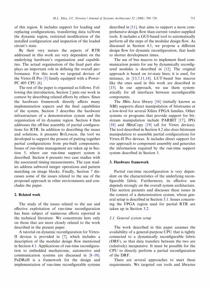
Fig. 1. Overview of the minimal demonstrator system setup.
712 M.L. Silva, J.C. Ferreira / Journal of Systems Architecture 52 (2006) 709–726
at Virtex-II Pro FPGAs. Most1 members of thisdevice family contain at least one PowerPC 405 coreimmersed in the reconfigurable fabric. An alterna-tive approach might implement the CPU by usingthe reconfigurable resources. In the case of Xilinxdevices, the Microblaze soft processor core [5] canbe used for this purpose. In our case, we used aboard with a XC2VP7 FPGA and 32 MB of exter-nal static memory.
An overview of a minimal system setup is shownin Fig. 1. It corresponds roughly to the actual floor-plan of the system. All modules except the CPU areimplemented in the reconfigurable fabric. The on-chip inter-module connections are an implementa-tion of the CoreConnect Bus Architecture [20] asprovided by the Xilinx Embedded DevelopmentKit (EDK). The two busses used are the ProcessorLocal Bus (PLB) and the lower-performance, butless resource-consuming, On-Chip Peripheral Bus(OPB).
The PLB connects to a memory controller for on-chip memory and to the PLB-OPB bridge. The OPBconnects to the external memory controller and tothe serial port. Using the OPB instead of the PLBto access external memory requires a much smallercontroller.
The two modules directly relevant for the presentwork are also connected to the OPB: the configura-tion memory controller (CMC) and the dynamicregion. The CMC is included in the EDK and pro-vides a wrapper around the Internal ConfigurationAccess Port (ICAP), a dedicated block available inseveral Xilinx device families.
The dynamic region is connected to the OPBthrough a wrapper module, the OPB dock. Forany given design the OPB dock is fixed; however dif-ferent docks may be used in different projects andboth development tools (like BITLINKER) and sup-port libraries must take this into account. The wrap-per is assigned a fixed range of the OPB addressspace and acts like an OPB slave peripheral, per-forming address decoding and I/O operations. Thewrapper also stores incoming data, so that it is keptavailable for processing by the components in thedynamic region between write operations.
The data communications between the wrapperand the dynamic region are made through a connec-tion interface with two separate unidirectional chan-
1 The XC2VP2 device is the exception: it contains no embeddedCPU core.
nels for write and read operations. Since the OPB isa 32-bit bus, each channel is 32 bits wide. The con-nection interface generates an additional signal thatindicates the occurrence of a write operation. Thissignal can be used as a clock enable signal for allflip-flops in the dynamic region.
The connection interface is implemented as ahard macro, that has been previously placed androuted. The use of such a ‘‘bus macro’’ avoids theneed for routing adjustments at run-time, whichwould otherwise be necessary to match the circuitsof the dynamic region to the OPB dock. The down-side is that modules designed for a specific OPBdock cannot, in general, be used with a differentone.
The application note [12] describes the implemen-tation of a bus macro using tri-state buffers and theassociated long lines available in several Xilinxdevice families.2 This approach has been used inseveral works [13,8,11] and in the initial version ofour system. However, this approach suffers fromlimitations due to the internal architecture of thedevices: (i) there are only four tri-state lines perCLB row; (ii) only one tri-state line can be used asinput by each CLB. The first condition implies thata module needing to access 32 bits would need to beat least 8 CLBs high. That is about 1/3 of the heightof the dynamic region available in the demonstra-tion system. The second condition makes the inter-nal routing of the dynamic region modules moredifficult. Also, recent device families like the Spar-tan-3 and Virtex-4 do not have tri-state lines.
An alternative is to use LUTs in the constructionof the connection region, as presented in [21,15].The basic element of the LUT-based bus macro isa fixed connection between LUTs in adjacent CLBs
2 Long lines associated with tri-state buffers are segmentedinterconnections that run the whole width of the device.

Fig. 2. Organisation of LUT-based bus macros.
Fig. 3. Organisation of the bus macro connections used in thedemonstration system.
M.L. Silva, J.C. Ferreira / Journal of Systems Architecture 52 (2006) 709–726 713
(see Fig. 2(a)). The LUTs operate in route-throughmode: their output is always equal to a specificinput. One LUT belongs to the CLB in the connec-tion interface of the dock; the other belongs to acomponent in the dynamic region. Each connectionis unidirectional: for a connection from the dock tothe dynamic region the source LUT is in the OPBdock and the sink LUT is in the dynamic region;for a connection in the other direction, the roles ofsink and source are reversed.
The connection may also be done through a flip-flop of the source CLB. In this case we obtain regis-tered connections as shown in Fig. 2(b). The LUT inthe source CLB can still be used for other purposes.This simplifies the design of components for pipelinestages.
In contrast to the restrictions associated with tri-state lines, the outputs of the destination LUT canbe connect as needed. However, the use of thisapproach requires that the CLBs participating inthe connection be adjacent to each other, either ver-tically or horizontally.
The connection interface used in the OPB dockof the demonstration system is based on horizontalunregistered connections. The same mechanism isalso used for communication between dynamicregion components. In that context, vertical connec-tions can also be used. The case studies of Section 6contain some examples. A detailed discussion ofdynamically reconfigurable pipelines based on verti-cal registered connections between stages can befound in [22].
The organisation of the connection interfacemust be chosen according to the needs of the appli-cation. As an example, Fig. 3 shows the connectioninterface used for the case studies of Section 6.There are 32 input and 32 out signals. As additionalsignal that indicates the occurrence of an OPB writeoperation is available at four outputs evenly distrib-uted along the dock. The signal is available at sev-eral outputs to ensure that it can be easily

Table 1Resource usage for the demonstration system
Peripheral Slices LUTs Flip flops BRAMs
PLB Arbiter 223 (5%) 334 54PLB Bram
Controller177 (4%) 136 249 16
PLB to OPBBridge
524 (11%) 487 519
OPB Arbiter 43 (1%) 53 6OPB SDRAM
Controller378 (8%) 510 295
OPB Dock 77 (2%) 50 128OPB HWICAP 153 (3%) 208 155 1OPB UART 64 (1%) 94 58OPB GPIO 77 (2%) 48 99Reset Block 48 (1%) 28 51
Total 1764 (36%) 1948 1614 17
714 M.L. Silva, J.C. Ferreira / Journal of Systems Architecture 52 (2006) 709–726
connected to the clock enable circuitry of thedynamic region. This signal is useful for synchronis-ing pipeline operations with OPB data transfers.
Ideally, the same connection interface is used formost applications. Nevertheless, there may be situa-tions that require the use of an OPB dock that dif-fers in the position of the connections to thedynamic area. As discussed in the next section, thework involved in creating a new version of a compo-nent adapted to a different interface is normallysmall, since it only involves changing the bus macro.It is easy to produce multiple versions of a compo-nent that differ only in the positions of the intercon-nections. Care must be taken during systemassembly to ensure that the version correspondingto the actual connection interface is used.
Resource usage in our demonstration setup isshown in Table 1. The CPU clock frequency is200 MHz. Both the PLB and the OPB operate at50 MHz. The dynamic region available in the dem-onstrator contains 28 · 11 = 308 CLBs3 and 6Blocks SelectRAM (BRAMs) of 18 K bits each.Larger devices might use the additional area for alarger single dynamic region or for several smallerones.
3.2. Dynamic region components
A dynamic region component may use almostany resource available in the dynamic region. Place-
3 Virtex-II Pro configurable logic blocks (CLB) include fourslices, each with two 4-input lookup-tables (LUT) and two flip-flops.
ment and routing of the component’s circuitry mustbe restricted to an area that can be fitted into thedynamic region. Since placement and routing usingthe vendor-supplied tools can only be restricted torectangular areas, it follows that a component mustalso have a rectangular shape. Rectangular compo-nents are also much easier to fit together.
The design of components can be split in twoparts: the design of the desired core functionalityand the design of its communication ports (i.e.,bus macros). The approach used in our work is tocreate the component’s core as an independentdesign and to combine it later with a wrapper imple-menting the desired connection pattern. Using thisapproach it is straightforward to design componentsthat differ only in the structure of their connectionsto other components. In addition, components withsimilar patterns can use the same wrappers.
The component’s core can be designed with theregular development tools. The configuration bit-stream that results from this process is targeted ata specific area of the reconfigurable fabric. Individ-ual components are assembled together to producethe configurations that are loaded onto the dynamicregion at run-time. (The assembly process isdescribed in detail in Section 4). In general, the com-ponents are not placed at the location specified intheir implementation process. Instead, they are relo-cated appropriately during the assembly process, sothat they fit inside the dynamic region and are cor-rectly connected.
Fig. 4 illustrates some possible arrangements ofcomponents. Example (a) shows three componentsconnected directly to the OPB dock; the bottomtwo are also connected together by a vertical con-nection interface. Example (b) shows an assemblywith two large components: one of them (compo-nent M2) is directly connected to the OPB dock;the other one (labelled M1) communicates withthe dock through a feed-through block F (through
Fig. 4. Examples of different possible component arrangementsinside a dynamic area.
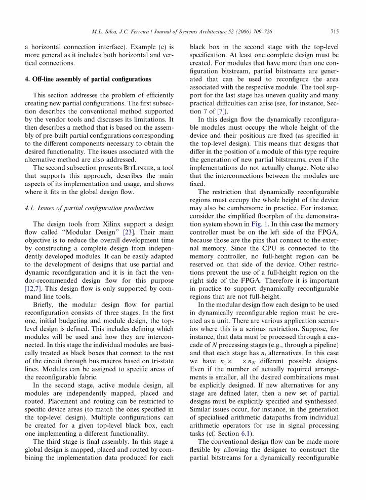
M.L. Silva, J.C. Ferreira / Journal of Systems Architecture 52 (2006) 709–726 715
a horizontal connection interface). Example (c) ismore general as it includes both horizontal and ver-tical connections.
4. Off-line assembly of partial configurations
This section addresses the problem of efficientlycreating new partial configurations. The first subsec-tion describes the conventional method supportedby the vendor tools and discusses its limitations. Itthen describes a method that is based on the assem-bly of pre-built partial configurations correspondingto the different components necessary to obtain thedesired functionality. The issues associated with thealternative method are also addressed.
The second subsection presents BITLINKER, a toolthat supports this approach, describes the mainaspects of its implementation and usage, and showswhere it fits in the global design flow.
4.1. Issues of partial configuration production
The design tools from Xilinx support a designflow called ‘‘Modular Design’’ [23]. Their mainobjective is to reduce the overall development timeby constructing a complete design from indepen-dently developed modules. It can be easily adaptedto the development of designs that use partial anddynamic reconfiguration and it is in fact the ven-dor-recommended design flow for this purpose[12,7]. This design flow is only supported by com-mand line tools.
Briefly, the modular design flow for partialreconfiguration consists of three stages. In the firstone, initial budgeting and module design, the top-level design is defined. This includes defining whichmodules will be used and how they are intercon-nected. In this stage the individual modules are basi-cally treated as black boxes that connect to the restof the circuit through bus macros based on tri-statelines. Modules can be assigned to specific areas ofthe reconfigurable fabric.
In the second stage, active module design, allmodules are independently mapped, placed androuted. Placement and routing can be restricted tospecific device areas (to match the ones specified inthe top-level design). Multiple configurations canbe created for a given top-level black box, eachone implementing a different functionality.
The third stage is final assembly. In this stage aglobal design is mapped, placed and routed by com-bining the implementation data produced for each
black box in the second stage with the top-levelspecification. At least one complete design must becreated. For modules that have more than one con-figuration bitstream, partial bitstreams are gener-ated that can be used to reconfigure the areaassociated with the respective module. The tool sup-port for the last stage has uneven quality and manypractical difficulties can arise (see, for instance, Sec-tion 7 of [7]).
In this design flow the dynamically reconfigura-ble modules must occupy the whole height of thedevice and their positions are fixed (as specified inthe top-level design). This means that designs thatdiffer in the position of a module of this type requirethe generation of new partial bitstreams, even if theimplementations do not actually change. Note alsothat the interconnections between the modules arefixed.
The restriction that dynamically reconfigurableregions must occupy the whole height of the devicemay also be cumbersome in practice. For instance,consider the simplified floorplan of the demonstra-tion system shown in Fig. 1. In this case the memorycontroller must be on the left side of the FPGA,because those are the pins that connect to the exter-nal memory. Since the CPU is connected to thememory controller, no full-height region can bereserved on that side of the device. Other restric-tions prevent the use of a full-height region on theright side of the FPGA. Therefore it is importantin practice to support dynamically reconfigurableregions that are not full-height.
In the modular design flow each design to be usedin dynamically reconfigurable region must be cre-ated as a unit. There are various application scenar-ios where this is a serious restriction. Suppose, forinstance, that data must be processed through a cas-cade of N processing stages (e.g., through a pipeline)and that each stage has ni alternatives. In this casewe have n1 · � � � · nN different possible designs.Even if the number of actually required arrange-ments is smaller, all the desired combinations mustbe explicitly designed. If new alternatives for anystage are defined later, then a new set of partialdesigns must be explicitly specified and synthesised.Similar issues occur, for instance, in the generationof specialised arithmetic datapaths from individualarithmetic operators for use in signal processingtasks (cf. Section 6.1).
The conventional design flow can be made moreflexible by allowing the designer to construct thepartial bitstreams for a dynamically reconfigurable
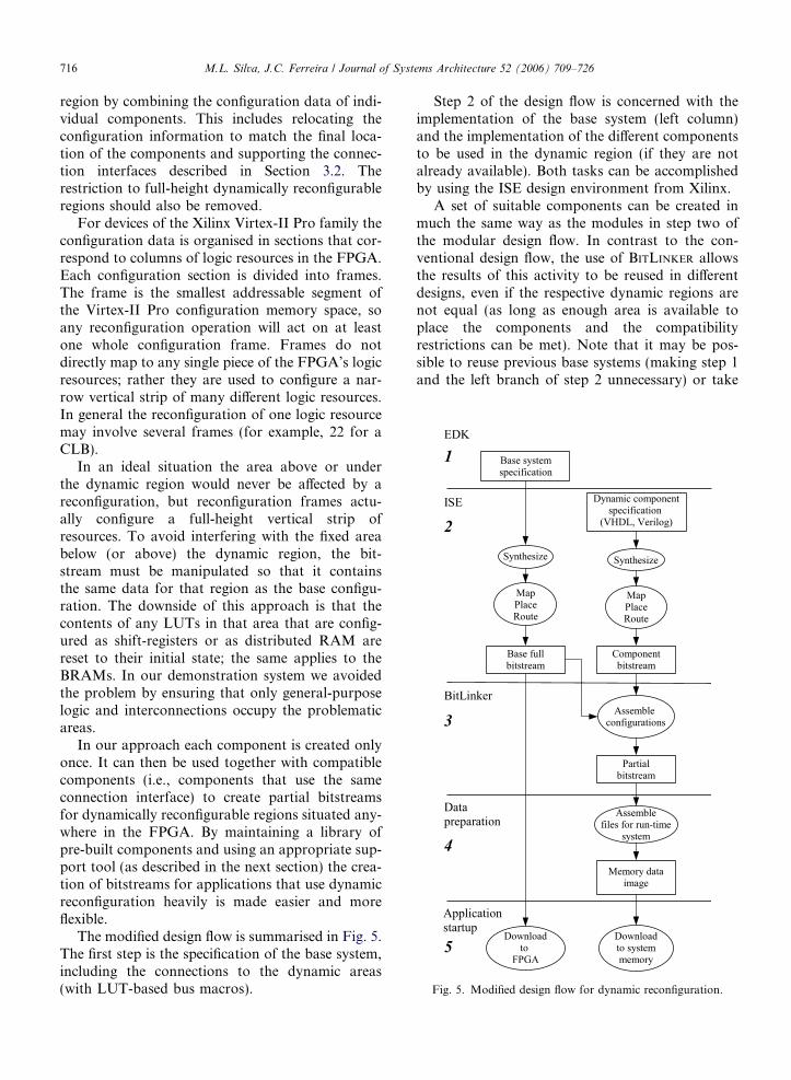
Fig. 5. Modified design flow for dynamic reconfiguration.
716 M.L. Silva, J.C. Ferreira / Journal of Systems Architecture 52 (2006) 709–726
region by combining the configuration data of indi-vidual components. This includes relocating theconfiguration information to match the final loca-tion of the components and supporting the connec-tion interfaces described in Section 3.2. Therestriction to full-height dynamically reconfigurableregions should also be removed.
For devices of the Xilinx Virtex-II Pro family theconfiguration data is organised in sections that cor-respond to columns of logic resources in the FPGA.Each configuration section is divided into frames.The frame is the smallest addressable segment ofthe Virtex-II Pro configuration memory space, soany reconfiguration operation will act on at leastone whole configuration frame. Frames do notdirectly map to any single piece of the FPGA’s logicresources; rather they are used to configure a nar-row vertical strip of many different logic resources.In general the reconfiguration of one logic resourcemay involve several frames (for example, 22 for aCLB).
In an ideal situation the area above or underthe dynamic region would never be affected by areconfiguration, but reconfiguration frames actu-ally configure a full-height vertical strip ofresources. To avoid interfering with the fixed areabelow (or above) the dynamic region, the bit-stream must be manipulated so that it containsthe same data for that region as the base configu-ration. The downside of this approach is that thecontents of any LUTs in that area that are config-ured as shift-registers or as distributed RAM arereset to their initial state; the same applies to theBRAMs. In our demonstration system we avoidedthe problem by ensuring that only general-purposelogic and interconnections occupy the problematicareas.
In our approach each component is created onlyonce. It can then be used together with compatiblecomponents (i.e., components that use the sameconnection interface) to create partial bitstreamsfor dynamically reconfigurable regions situated any-where in the FPGA. By maintaining a library ofpre-built components and using an appropriate sup-port tool (as described in the next section) the crea-tion of bitstreams for applications that use dynamicreconfiguration heavily is made easier and moreflexible.
The modified design flow is summarised in Fig. 5.The first step is the specification of the base system,including the connections to the dynamic areas(with LUT-based bus macros).
Step 2 of the design flow is concerned with theimplementation of the base system (left column)and the implementation of the different componentsto be used in the dynamic region (if they are notalready available). Both tasks can be accomplishedby using the ISE design environment from Xilinx.
A set of suitable components can be created inmuch the same way as the modules in step two ofthe modular design flow. In contrast to the con-ventional design flow, the use of BITLINKER allowsthe results of this activity to be reused in differentdesigns, even if the respective dynamic regions arenot equal (as long as enough area is available toplace the components and the compatibilityrestrictions can be met). Note that it may be pos-sible to reuse previous base systems (making step 1and the left branch of step 2 unnecessary) or take

M.L. Silva, J.C. Ferreira / Journal of Systems Architecture 52 (2006) 709–726 717
components from previously defined libraries(making the tasks on the right branch of step 2unnecessary).
When a suitable set of pre-built components isavailable (made specifically for the application ortaken from an existing library), the next step ofthe design flow is to combine the components asdesired in order to obtain the partial bitstreamsfor the dynamic region. The chosen componentsmust be compatible with the dynamic region andwith each other. This means that they mustphysically fit in the dynamic area and possesscompatible interface connections. The adjacencyrestrictions discussed in Section 3.2 must be met.Support for this stage is provided by the BITLIN-
KER tool that we developed; it is described in thenext section.
Steps 4 and 5 deal with the preparation of datafor the run-time support system and applicationstartup; this is discussed further in Section 5.
4.2. The implementation of BITLINKER
Our current BITLINKER implementation is a Javaapplication with a command line interface. It usesthe JBits 3.0 library from Xilinx. JBits is an Appli-cation Program Interface (API) to the Xilinx config-uration bitstream. The distributed version does notsupport Virtex-II Pro devices, but it does supportthe Virtex-II family. The reconfigurable fabric ofboth families is similar, so it was possible to adaptthe library to our needs.
The main requirements for BITLINKER fol-low from the previous discussion. They are thefollowing:
• the configuration information of the individualcomponents must be extracted from the corre-sponding complete bitstream;
• the component modules must be relocated. Itshould be possible for the extracted componentto be assigned to any compatible section of thedynamic region;
• the tool must be able to process multiple compo-nents and to use the same component multipletimes;
• the tool must ensure that the created bitstream isadapted to the structure of the dynamic area.For example, the dynamic area does not extendto the bottom of the FPGA in our case, and sothe resulting partial bitstream must completethe information according to the base system;
• the tool must perform area compatibility tests,i.e. it must check if the destination area for therelocated components is compatible with thecomponents’ original area. All the resourcesrequired by a component must be available atthe destination in the same relative positions;
• BITLINKER must perform connection tests. Thecomponents communicate with the static areathrough a LUT-based bus macro; the tool mustverify that the destination location of a compo-nent is compatible with its bus macro;
• the tool must produce a correct partial reconfig-uration file for the whole area that is affectedby the reconfiguration. In general, this area willbe larger than the total area occupied by the indi-vidual components.
The area compatibility tests are important,because their omission might allow the productionof non-functional, but syntactically correct, bit-streams as a consequence of erroneous user specifi-cations. This would cause the configured devicenot to perform the intended functions, leading inthe worst case to contention on internal lines.
The general compatibility rule is that any usedresources from the region originally occupied bythe component must be available in the destinationregion at the same relative position. In this respectthe relevant resources are CLBs, BRAMs, Multipli-ers, IOBs (Input/Output Blocks), and all the associ-ated switch matrices. For instance, a module thatuses only CLBs must be positioned in a part ofthe dynamic region that only contains CLBs. Ifthe module spans a column of BRAMs, then itmay only be relocated to a target area that includesBRAMs at the same relative position. This may benecessary even when the module does not specifi-cally use the BRAMs, as long a BRAM’s switchmatrix is used for routing purposes.
Fig. 6 shows a conceptual model of BITLINKER’smain operation. The core task of BITLINKER is toextract (part of) the information from one bitstreamand merge it into another bitstream, possibly at adifferent position. By repeating the process frag-ments from multiple bitstream can be combined.Since the underlying reconfigurable fabric is highlyregular, relocation of components consists basicallyof composing the frames corresponding to the targetarea with the appropriate parts of the source fra-mes.This approach works well for almost all theresource types; only global resources like DLLsare not suitable for this kind of treatment.

Fig. 6. Conceptual model of a BITLINKER operation.
718 M.L. Silva, J.C. Ferreira / Journal of Systems Architecture 52 (2006) 709–726
The output of BITLINKER is a partial bitstreamcorresponding to the assembled configuration or avertical section thereof (see Fig. 7).The capabilityof extracting parts of an assembly can be used tocreate smaller bitstreams when assemblies havecommon components in the same positions. In theexample of Fig. 7 three assemblies have a commonvertical section on the right. It is possible to switchbetween the three assemblies by using the smallerbitstream (P1, P2 or P3) instead of using the threefull assemblies (F1, F2 or F3), as long as one ofthe complete assemblies is loaded at the beginning.
BITLINKER can compose all the bitstreams men-tioned in this example. A simple invocation ofBITLINKER may be as follows:
Fig. 7. Exploitation of commonalities between componentassemblies.
java BitLinker <device> <base file><output file> <range> [<component_1><component_2> � � �<component_n>]
The first argument to BITLINKER specifies thetype of device used, and the second the bitstreamof the base system. The third argument specifiesthe name of the output file, followed by the rangeof columns of the configuration assembly sectionto be written to the output bitstream. Next comethe specifications of the components (bitstream fileand source location) and of the respective targetpositions; multiple components can be specified.Since the command line can easily become verylong, BITLINKER is able to read the component spec-ifications from a file.
5. Run-time support system
The use of partial configurations at run-timerequires the availability of extra information besidesthe configuration itself. The information requiredand its use are treated in the first part of this section.The second part describes the library of supportfunctions that we developed, and illustrates its uses.The timing of the different operations and guidelinesfor their use are also presented.
5.1. Information for run-time management
of partial reconfigurations
A bitstream generated by BITLINKER containsone or more components, some of which may becopies of the same original component. In additionto the bitstream itself, an application needs otherinformation, like what components are available,their positions and their connections to the OPBdock. For suitably designed components, the logicfunctions they implement may be altered by chang-ing the contents of specific LUTs. To support thiscapability the run-time system must have informa-tion about which LUTs can be altered and what val-ues they may be set to.
BITLINKER is able to generate two types of bit-streams for a specified sector of the reconfigurableregion. To understand the reason for this, it is neces-sary to keep in mind that each configuration frameonly affects a small vertical strip of physicalresources. It is therefore common for frames in theassembled design to be identical to the frames ofthe base system (i.e., of an ‘‘empty’’ dynamic region).In this case, the common frames can be omitted from

M.L. Silva, J.C. Ferreira / Journal of Systems Architecture 52 (2006) 709–726 719
the assembled bitstream, thus reducing its size. Thismay be useful in situations where the memoryavailable to hold the configuration data is limited.
However, the use of such a bitstream requires therun-time system to ensure that the correspondingarea is in the base state before loading the data. Thisis done by loading the bitstream for the ‘‘empty’’dynamic region before loading the minimal bit-stream. Therefore, there is a time penalty for thereduction in the size of the configuration data. Notethat the configuration data available to the applica-tion must now include the configuration data for an‘‘empty’’ dynamic region.
Depending on the specific application and theavailable system memory, the designer may chooseto work with minimal bitstreams or with bitstreamsthat contain all the configuration data for the rele-vant sector of the dynamic region. BITLINKER sup-ports the generation of the two types of bitstreams.
All relevant information for the run-time systemis gathered together with the bitstream in a speciallyformated file. Such a Component Assembly for Par-tial Reconfiguration (CAPR) file contains the fol-lowing information items:
• the bitstream type – there are three types: the bit-stream for an empty dynamic region (base state),a bitstream with complete information for a sec-tor, or a minimal bitstream;
• component assembly identification number – aunique 32-bit number for each component usedby the implemented application;
• the range of columns occupied by the com-ponents(s);
• the size of the partial bitstream, in bytes;• the number of components in the assembly.
The remaining items are repeated for each com-ponent in the assembly:
• connection range – this parameter gives informa-tion about the locations where the componentconnects to the dock, and also the number ofinputs and outputs;
• the range of rows occupied by the component;• the number of modifiable LUTs in the com-
ponent;• relative coordinates of the modifiable LUTs.
It is also convenient to define sets of values thatmay be loaded to specific LUTs. Typically each suchset corresponds to a mode of operation of the cir-
cuit. To support this functionality two more itemsmay be present:
• the number of sets of values;• each set of values (for the modifiable LUTs pre-
viously specified in the file).
The CAPR files are generated by an auxiliaryprogram, that, like BITLINKER, is written in Javaand uses the JBits API. The program takes as argu-ments the bitstream generated by BITLINKER, thebitstream for the base system and a text file specify-ing the properties of the first bitstream.
All the CAPR files for an application are kept inthe on-board static RAM memory as files of a Lib-Xil Memory File System, a simple memory-basedfile system supported by EDK. A file system imageis prepared off-line in the host system and thendownloaded to the board together with the applica-tion code. From the application’s perspective theCAPR files can be accessed like regular files. Theproduction of the CAPR files and file system imageconstitutes step 4 of the design flow shown previ-ously in Fig. 5.
5.2. Library organisation and characteristics
Our run-time library allows an application to:
• load or remove component assemblies from thedynamic area (including the re-initialisation ofparts of the dynamic area for the use of minimalbitstreams when required);
• read or remove CAPR files from the on-boardmemory;
• transfer data to and from an installed componentassembly;
• read and write LUTs labelled as modifiable;• list available assemblies and their properties;• automatically identify assemblies available in a
file system image.
The run-time library is written in C and uses thefollowing components of the software package thatships with EDK [24]: Standalone Board SupportPackage, Standard C Libraries, LibXil Memory FileSystem, LibXil File, and LibXil Drivers. Internally,the library includes a data manager, a reconfigura-tion manager and an input/output manager. Thedata manager enables applications to access theCAPR files residing in the external on-board mem-ory. It may also be used to erase files that are no

Table 2Experimental data transfer times to/from the dynamic region(average values): (a) from/to CPU; (b) from/to external memory
Number of operations Average time per operation (ls)
Write Read Write/read
(a)1 4.44 4.36 5.06
10 0.66 0.72 1.05100 0.30 0.36 0.66
1000 0.26 0.32 0.6210000 0.26 0.32 0.62
100000 0.26 0.32 0.62
(b)1 4.80 4.90 5.66
10 1.95 1.84 2.56100 1.67 1.56 2.21
1000 1.65 1.52 2.1810000 1.65 1.52 2.18
100000 1.65 1.52 2.18
The last column in each table shows the time taken per operation(a read or a write) when writes and reads are interleaved.
720 M.L. Silva, J.C. Ferreira / Journal of Systems Architecture 52 (2006) 709–726
longer needed in order to free memory for otheruses.
The reconfiguration manager provides higher-level functions for performing reconfiguration. Itbasically encapsulates the use of the Xilinx OPBHWICAP driver, providing the functions necessaryfor the reconfiguration of dynamic regions and themodification of the contents of LUTs. The state ofany flip-flop of the dynamic region can also beinspected.
The input/output manager provides functions tosend and receive data to/from the componentassemblies. These functions determine the correctmemory-mapped I/O address, perform the I/Otransaction and convert the data to/from applica-tion-specified formats.
Fig. 8 shows a very small code fragment from oneof the case studies. The code exemplifies the typicalcalls to the run-time library. First there is call toload a configuration specified by its unique identifi-cation number. Then there is a call to change thevalue of a modifiable LUT. Three coordinates spec-ify where the modifiable LUT is, while the fourthargument specifies the new value (a 16-bit number).The remaining fragments show part of a loop thatsends data values from an image to the dynamicarea and reads back the result.
The effective use of dynamic reconfiguration in aparticular application depends on the time it takesto perform data transfers and reconfiguration oper-ations, including both the software overheads andthe delays introduced by the hardware organisation(like bus and controller delays). In order to obtainrelevant timing information for the run-time sup-port system, some simple timing experiments werecarried out. The device used was a Virtex-II ProXC2VP7-6FG456. The embedded PowerPC 405CPU runs at 200 MHz. Both the PLB and the
Mod_LoadConfig(1); /* load component...ModRec_SetLut(col, row, lut, lutvalu...for(i = 0; i<ncols; i++ ){
for(j = 0; j<nrows; j++ ){...Mod_SendData(1, image[j][i]);/*...data = Mod_ReadData(1); /* read...
}}
Fig. 8. Example applicat
OPB have a 50 MHz clock. All timings were mea-sured by using the clock cycle counters availablein the CPU.
In order to obtain a lower bound on data transfertimes, we measured the time necessary to transfersequences of 32-bit values (since the OPB is a 32-bit bus). Table 2 shows the results for differenttransfer sizes and two different data sources: Table2(a) shows the timings (per operation) for transfersbetween CPU and dynamic area; Table 2(b) showsthe corresponding values for transfers betweenexternal memory and dynamic area. In the secondcase, the results include the time necessary to accessexternal memory via a memory controller connectedto the OPB. The overhead of the controlling soft-ware is included in all cases.
assembly 1 */
e); /* change contents of LUT */
write data to assembly 1 */
data from assembly 1 */
ion code fragment.
M.L. Silva, J.C. Ferreira / Journal of Systems Architecture 52 (2006) 709–726 721
The timed needed to reconfigure a section of theFPGA depends only on the number of framesrequired. The measurements performed on the dem-onstration system produced an average reconfigura-tion time per frame of 3028 ls. Just copying the datato the BRAM inside the CMC takes 2036 ls (67%of the reconfiguration time); the remaining time istaken up by the ICAP to perform the actual config-uration. The reconfiguration of the whole dynamicarea requires 12 · 22 frames plus an additionalpad frame (265 frames in total), so the whole recon-figuration takes 0.8 s. If the configuration data istaken from the CAPR file in external RAM, anadditional data preparation time is required.
The transfer times of Table 2 allow the applica-tion developer to estimate a lower bound for theminimum time necessary to process a given amountof data. The lower bound assumes that the timetaken by a circuit in the dynamic region to processthe data is dominated by the time taken to transferthe data to/from the dynamic region.
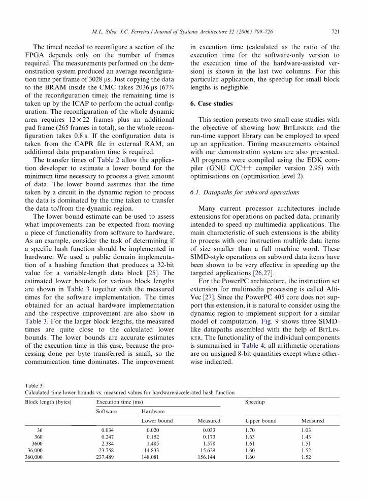
The lower bound estimate can be used to assesswhat improvements can be expected from movinga piece of functionality from software to hardware.As an example, consider the task of determining ifa specific hash function should be implemented inhardware. We used a public domain implementa-tion of a hashing function that produces a 32-bitvalue for a variable-length data block [25]. Theestimated lower bounds for various block lengthsare shown in Table 3 together with the measuredtimes for the software implementation. The timesobtained for an actual hardware implementationand the respective improvement are also show inTable 3. For the larger block lengths, the measuredtimes are quite close to the calculated lowerbounds. The lower bounds are accurate estimatesof the execution time in this case, because the pro-cessing done per byte transferred is small, so thecommunication time dominates. The improvement
Table 3Calculated time lower bounds vs. measured values for hardware-accele
Block length (bytes) Execution time (ms)
Software Hardware
Lower bound
36 0.034 0.020360 0.247 0.152
3600 2.384 1.48536,000 23.758 14.833
360,000 237.489 148.081
in execution time (calculated as the ratio of theexecution time for the software-only version tothe execution time of the hardware-assisted ver-sion) is shown in the last two columns. For thisparticular application, the speedup for small blocklengths is negligible.
6. Case studies
This section presents two small case studies withthe objective of showing how BITLINKER and therun-time support library can be employed to speedup an application. Timing measurements obtainedwith our demonstration system are also presented.All programs were compiled using the EDK com-piler (GNU C/C++ compiler version 2.95) withoptimisations on (optimisation level 2).
6.1. Datapaths for subword operations
Many current processor architectures includeextensions for operations on packed data, primarilyintended to speed up multimedia applications. Themain characteristic of such extensions is the abilityto process with one instruction multiple data itemsof size smaller than a full machine word. TheseSIMD-style operations on subword data items havebeen shown to be very effective in speeding up thetargeted applications [26,27].
For the PowerPC architecture, the instruction setextension for multimedia processing is called Alti-Vec [27]. Since the PowerPC 405 core does not sup-port this extension, it is natural to consider using thedynamic region to implement support for a similarmodel of computation. Fig. 9 shows three SIMD-like datapaths assembled with the help of BITLIN-
KER. The functionality of the individual componentsis summarised in Table 4; all arithmetic operationsare on unsigned 8-bit quantities except where other-wise indicated.
rated hash function
Speedup
Measured Upper bound Measured
0.033 1.70 1.030.173 1.63 1.431.578 1.61 1.51
15.629 1.60 1.52156.144 1.60 1.52

Fig. 9. Datapaths for SIMD-like processing of small data items.
Table 4Subword operations used in the case study
Symbol Operation
S1 Saturating addition with signed constantS2 Saturating additionS3 Saturating subtractionM1 Saturating multiplication with constantP 32 bit unsigned accumulatorF Feedthrough components
All data are assumed to be 8-bit unsigned quantities except wherespecified otherwise.
722 M.L. Silva, J.C. Ferreira / Journal of Systems Architecture 52 (2006) 709–726
The datapath of Fig. 9(a) implements the coreoperation for brightness adjustment of an image:it receives four 8-bit unsigned values and adds toeach one a signed constant value (with saturationof the final result). The constant is set by program-ming specific LUTs inside each component. Fouroutput pixel values are produced simultaneously.
The first example operates on just one image. Theother two take values from two images and combinethem. The assembly of Fig. 9(b) is used for the addi-tive blending of two images. In the setup used, fourinput pixel values (two from each image) producetwo output values. In order to reduce the numberof read accesses to the dynamic region, the valuesof two successive processing steps are stored inmutually exclusive 16-bit sections of a 32-bit register(component P) and are read out together. In thisway the number of read accesses is the absolute min-
Table 5Timing measurements for tasks based on subword operations
Task Execution time per output pixel
Software Hardwa
Lower
Brightness adjustment 2.18 0.55Additive blending 2.96 0.96Fade effect 3.94 0.96
imum required (one fourth the number of outputpixels).
The third example (Fig. 9(c)) performs the coreoperations necessary to obtain a fade-in–fade-outeffect between to images by implementing theexpression (A � B) · f + B, where A is a pixel valuefrom the first image, B is a pixel value from the sec-ond, and f is a constant value that specifies the rel-ative contribution of the first image to the result[26]. The complete fade-in–fade-out effect isobtained by repeatedly processing the same twosource images for diminishing values of f. The com-plete fade-in-fade-out effect terminates when f = 0.In the implementation of Fig. 9(c) the value of f
can be changed by adjusting LUT values in theM1 component. Note further that the S3 and M1components also act as feed-throughs: one of theinputs is passed unchanged to one of the outputs.This is necessary in order to have the B value avail-able for the last addition in S2.
The timing measurements obtained with the dem-onstration system are shown in Table 5. The valuesreported are average values (per output pixel) mea-sured for different image sizes (8-bit pixels). Asexpected, the image sizes have no noticeable influ-ence on the time taken to produce each output pixelvalue, so only the average values are shown. Thetime necessary to set a value of f in the third exam-ple is not included.
The speedups obtained in the first task are largerthan the others, because less data has to be trans-ferred to the dynamic region per output value.The measured improvement is mainly attributableto the capability to process 4 pixel values concur-rently. The lower bound calculated for this task byusing the values reported in Section 5.2 is in goodagreement with the actual results.
The third task shows a larger improvement thanthe second one, because the complexity of the func-tionality implemented in hardware is greater in thelatter case (for identical data transfer requirements).
(ls) Speedupmeasuredre
bound Measured
0.55 4.01.27 2.31.38 2.9

Table 6Timing measurements for fade effect task
Image size Execution time per outputpixel (ls)
Speedup(measured)
Software Hardware
Lowerbound
Measured
256 · 256 2.96 1.08 1.39 2.13256 · 512 2.96 1.02 1.33 2.23512 · 512 2.96 0.99 1.30 2.281024 · 1024 2.96 0.96 1.27 2.33
M.L. Silva, J.C. Ferreira / Journal of Systems Architecture 52 (2006) 709–726 723
In both cases, the measured values are about 30%worse than the lower bound. This can be explainedby noting that both tasks require data from two dif-ferent imaged to be merged by the CPU beforebeing sent to the dynamic area.
The impact of changing the value of f betweenfade operations can be observed from the valuesshown in Table 6, which include the time requiredfor that operation. The setting of f takes a fixedamount of time, therefore the actual size of theimage influences the average execution time perpixel. The measured speedups range between 2.1and 2.3. As expected, the impact of changing f
decreases with the image size.For these simple tasks the effectiveness of hard-
ware support in the present setup is limited by thedata transfer capacity to and from the dynamicregion. By connecting the dynamic region to the64-bit PLB (instead of using the 32-bit OPB), a dou-bling of the obtainable improvements can beexpected (for these straightforward examples). Alarger dynamic region would also help to obtain bet-ter improvements by allowing more complex func-tionality to be implemented. In the case of ourdemonstration system the third datapath almostfilled the dynamic region.
In order to obtain a quantitative indication of theperformance impact due to the use of a dynamicapproach as opposed to a fixed implementation,the additive blending task and the underlying sup-port system were implemented as one complete tra-ditional design. We removed the hardware ICAP,because no dynamic reconfiguration is performed,but kept the rest of the system. The resulting imple-mentation achieved a system bus frequency of56 MHz, a 12% improvement over the 50 MHz ofthe dynamic system (using only the standardoptions of the CAD tools). The bus frequency isthe most important factor affecting the performance
of this design, and its degradation can therefore betaken as a good indicator of the overall impact ofthe dynamic approach.
The current version of BITLINKER does not checkany timing constraints for the component assem-blies it produces. However, all components used inthe designs described in this section operate wellabove 50 MHz. The operation of the dynamic areais clocked by the write operations performedthrough the system bus, so the effective operationfrequency of the logic inside the dynamic area is,according to the values of Table 2, 0.26 ls/cycle = 3.85 MHz, 13 times slower than the busclock rate. In all the cases described, the largestdelay through any assembly used in the dynamicarea was comfortably below 0.26 ls.
6.2. Pattern matching in bilevel images
The second case study concerns the implementa-tion of basic pattern matching for bilevel images.The core function implemented in hardware countshow many pixels of an 8 · 8 bilevel image patternare equal to the corresponding pixels of a windowthat slides over a larger image. The pattern can bechanged at run-time by modifying the contents ofspecific LUTs. The implementation is based arounda pipeline of eight stages, each one calculating thenumber of matching pixels in a row of the pattern.The results of the eight stages are summed, produc-ing the number of matching pixels for one positionof the sliding window. The application uses thisnumber to decide if a match occurs.
Fig. 10 shows the structure of the assembleddesign. Each stage of the pipeline is built aroundthe same design: eight comparators are used todetermine if each input bit matches a value speci-fied by one of eight LUTs; the number of match-ing bits (in the range 0–8) is sent to the 4-bitoutput. From this core, three components wherederived (M1, M2 and M3), that implement the threetypes of stages used. The assembly includes a com-ponent (M4) that feeds the pipeline and adds upthe count of matching pixels from each pipelinestage.
The input stage (M1) has an 8-bit data input, an8-bit data output and an 4-bit sum output. Theinput connects to M4 through a horizontal connec-tion interface, the 8-bit output is used to pass a setof pixel values to the next component in the pipelineand the 4-bit sum output connects to the adder com-ponent. The second type of stage (M2) is used for

Fig. 10. Component assembly for block pattern-matching inbilevel images.
Table 7Measured speedups for hardware-assisted pattern matching inbilevel images
Image size Execution time (s) Speedup(measured)Software Hardware
Lowerbound
Measured
256 · 256 11.42 0.14 0.44 26.0256 · 512 23.12 0.29 0.84 27.5512 · 512 46.27 0.57 1.71 27.11024 · 1024 186.23 2.29 6.78 27.5
724 M.L. Silva, J.C. Ferreira / Journal of Systems Architecture 52 (2006) 709–726
the six intermediate stages: the only difference fromM1 is that its input uses a vertical connection inter-face to the previous component. The third type(M3) is used for the last stage: it has no 8-bit output.
Component M4 implements a tree of adders, thatadds up the counts from the pipeline stages and out-puts the result to the OPB dock.
BITLINKER was used to assemble the design intwo parts: one contains the pipeline (eight compo-nents with modifiable LUTs, six of which are iden-tical) and the other the combining output stage. Theseparation in two parts is not strictly necessary forthis example; it was carried out in order to allowthe use of the pipeline with other combining stages.The reconfiguration times for the two parts are0.23 s for the pipeline, and 0.29 s for the combiningstage.
The software part of the application loads thehardware design, sets up the LUTs according tothe pattern to be searched and then feeds the imagedata to the dynamic area.
The pattern matching application was first writ-ten entirely in software. For the hardware-assistedversion, the function that implements the core ofthe algorithm was modified to load the two partialbitstreams, configure the LUTs with the desired pat-tern, send the image data and retrieve the results.Image data is transferred to the dynamic regionaccording to a vertical sweep of the image. Aftersending one column of image data, the applicationmust refill the pipeline with data from the next col-umn before retrieving more results. An N · M
image results in N � 8 + 1 columns being processed,each one having M bytes.
Table 7 shows the results obtained withboth implementations for several image sizes. Theresults for the hardware-assisted implementationare clearly better, with an average speedup of 27.
Increasing the pipeline depth (which is equal tothe height of the pattern), although conceptuallytrivial, would require a higher dynamic area thanis available on the demonstrator. However, it is fea-sible to enlarge the pattern to a width of 16 bits (i.e.,to have an 8 · 16 pattern). Such an extension can beaccommodated within the current hardware’s tim-ing budget; the time taken by the software-only ver-sion would increase significantly.
7. Conclusion
The present paper addressed several issuesrelated to effectively supporting applications thatuse partial run-time reconfiguration, an approachto performance enhancement that may have wide-ranging applicability. Considerations of hardwareorganisation and of the basic characteristics of theemployed programmable devices are always presentwhen analysing the issues related to the exploitationof run-time reconfiguration, so the paper includedthe presentation of a minimal demonstrator systembased on a Virtex-II Pro platform FPGA and dis-cussed its more salient aspects.
Against this background, the paper described anapproach to the rapid production of partialdynamic configuration data, based on the relocationand assembly of previously created bitstreams ofindividual components, analysed the associatedrequirements and presented a tool called BITLINKER
that automates the assembly process.The paper also addressed the issue of providing
run-time support to applications for using partialconfiguration bitstreams like the ones produced by

M.L. Silva, J.C. Ferreira / Journal of Systems Architecture 52 (2006) 709–726 725
BITLINKER. Application support is provided by alibrary built on top of vendor-supplied basic func-tionality. Supported operations include the manage-ment of sets of related configurations, the loading ofspecific circuits, the execution of data transfers to/from the dynamically installed circuits (includingany necessary format conversions) and the alter-ation of the contents of symbolically specifiedrelocated LUTs. The paper included timing mea-surements of the basic library operations obtainedfrom the demonstration system.
Although the demonstration system used a Vir-tex-II Pro device, the approach is usable with sys-tems based on other devices that support partialRTR. The run-time support system is written instandard C, so it should be easily portable, as longas some basic functions for controlling the reconfig-uration are available. For instance, porting the sys-tem to a Virtex-II with a MicroBlaze soft processorcore would be straightforward. Similarly, porting toa system with an appropriate FPGA and externalCPU should not present any difficulties.
Porting BITLINKER may be more complicated.Since it is built on top of JBits, targeting Xilinxdevices supported by this library is relatively simple.This means that targeting systems with Virtex orVirtex-II devices is straightforward. For other sys-tems, a library for basic bitstream manipulationwould have to be implemented first. This wouldapply to systems based on Virtex-4 devices (not sup-ported by JBits) or on FPSLIC devices from Atmel.The development of such a library is a delicateendeavour, that would require a significant pro-gramming effort, as well as access to proprietaryinformation. Even if such a library was available,BITLINKER would still have to be adapted to thenew biststream organisation.
In order to clarify the proposed approach to per-formance enhancement, the paper included twosmall case studies. One concerned the creation anduse of datapaths for subword operations, while theother implemented a simple pattern matching taskon bilevel images. The reported timing measure-ments strengthen the case for the use of run-timereconfiguration and for its applicability to high-end embedded systems.
References
[1] M. Wirthlin, B. Hutchings, Improving functional densityusing run-time circuit reconfiguration, IEEE Trans. VeryLarge Scale Integrat. Syst. 6 (2) (1998) 247–256.
[2] S.A. Guccione, D. Levi, Design advantages of run-timereconfiguration, in: J. Schewel, P.M. Athanas, S.A. Gucci-one, S. Ludwig, J.T. McHenry (Eds.), ReconfigurableTechnology: FPGAs for Computing and Applications, Proc.SPIE, vol. 3844, SPIE, 1999, pp. 87–92.
[3] Xilinx, Virtex-II Pro Platform FPGA Handbook, October2002.
[4] Atmel, FPSLIC 5–40 K gates of AT40K FPGA with 8-bitAVR microcontroller, up to 36 k bytes of SRAM and on-chip JTAG ICE, datasheet, ref. 1138H-FPSLI-6/05, 2005.
[5] Xilinx, MicroBlaze Processor Reference Guide, June 2004.[6] Xilinx, PowerPC Processor Reference Guide, September
2003.[7] B. Blodget, C. Bobda, M. Hubner, A. Niyonkuru, Partial
and dynamically reconfiguration of Xilinx Virtex-II FPGAs,in: J. Becker, M. Platzner, S. Vernalde (Eds.), Proc. FPL’04,Lecture Notes in Computer Science, vol. 3203, Springer,2004, pp. 801–810.
[8] S. Toscher, R. Kasper, T. Reinemann, Dynamic reconfigu-ration of mechatronic real-time systems based on configura-tion state machines, in: Proc. IPDPS’05, IEEE ComputerSociety, 2005, p. 172b.
[9] M. Ullmann, M. Hubner, B. Grimm, J. Becker, An FPGArun-time system for dynamical on-demand reconfiguration,in: Proc. IPDPS’04, IEEE Computer Society, 2004, p. 135.
[10] E.L. Horta, J.W. Lockwood, D.E. Taylor, D. Parlour,Dynamic hardware plugins in an FPGA with partial run-time reconfiguration, in: Proc. DAC’02, ACM, 2002, pp.343–348.
[11] E. Carvalho, N. Calazans, E. Briao, F. Moraes, PaDReH: aframework for the design and implementation of dynami-cally and partially reconfigurable systems, in: Proc.SBCCI’04, ACM Press, New York, NY, USA, 2004, pp.10–15.
[12] Xilinx, Two flows for partial reconfiguration: module base orsmall bit manipulations, Application Note 290, September2004.
[13] S. Ihmor, W. Hardt, Runtime reconfigurable interfaces – theRTR-IFB approach, in: IEEE Computer Society, 2004, p.136a.
[14] T. Marescaux, A. Bartic, D. Verkest, S. Vernalde, R.Lauwereins, Interconnection networks enable fine-graindynamic multi-tasking on FPGAs, in: M. Glesner, P. Zipf,M. Renovell (Eds.), Proc. FPL’02, Lecture Notes in Com-puter Science, vol. 2438, Springer, 2002, pp. 795–805.
[15] M. Huebner, T. Becker, J. Becker, Real-time LUT-basednetwork topologies for dynamic and partial FPGA self-reconfiguration, in: Proc. SBCCI’04, ACM Press, New York,NY, USA, 2004, pp. 28–32.
[16] S.A. Guccione, D. Levi, XBI: a Java-based interface toFPGA hardware, in: J. Schewel (Ed.), Configurable Com-puting: Technology and Applications, Proc. SPIE, vol. 3526,SPIE, 1998, pp. 97–102.
[17] E.L. Horta, J.W. Lockwood, S.T. Kofuji, Using PARBIT toimplement partial run-time reconfigurable systems, in: M.Glesner, P. Zipf, M. Renovell (Eds.), Proc. FPL’02, LectureNotes in Computer Science, vol. 2438, Springer-Verlag,London, UK, 2002, pp. 182–191.
[18] A.K. Raghavan, P. Sutton, JPG – a partial bitstreamgeneration tool to support partial reconfiguration in VirtexFPGAs, in: Proc. IPDPS’02, IEEE Computer Society,Washington, DC, USA, 2002, p. 192.

726 M.L. Silva, J.C. Ferreira / Journal of Systems Architecture 52 (2006) 709–726
[19] M. Dyer, C. Plessl, M. Platzner, Partially reconfigurablecores for Xilinx Virtex, in: M. Glesner, P. Zipf, M. Renovell(Eds.), Proc. FPL’02, Lecture Notes in Computer Science,vol. 2438, Springer, 2002, pp. 292–301.
[20] IBM, The CoreConnect bus architecture, white paper,September 1999.
[21] A. Upegui, R. Moeckel, E. Dittrich, A. Ijspeert, E. Sanchez,An FPGA dynamically reconfigurable framework for mod-ular robotics, in: U. Brinkschulte (Ed.), Workshop Proceed-ings of the 18th International Conference on Architecture ofComputing Systems (ARCS’05), VDE Verlag, Berlin, 2005,pp. 83–89.
[22] M.L. Silva, J.C. Ferreira, Using a tightly-coupled pipeline indynamically reconfigurable platform FPGAs, in: Proc.DSD’05, IEEE Computer Society, Porto, Portugal, 2005,pp. 383–386.
[23] Xilinx, Development System Reference Guide, 2004.[24] Xilinx, EDK OS and Libraries Reference Guide, March
2004.[25] B. Jenkins, Hash functions, Dr. Dobb’s J. (9) (1997) 107–
109.[26] A. Peleg, S. Wilkie, U. Weiser, Intel MMX for multimedia
PCs, Commun. ACM 40 (1) (1997) 24–38.[27] K. Diefendorff, P. Dubey, R. Hochsprung, H. Scale, AltiVec
extension to PowerPC accelerates media processing, IEEEMicro 20 (2) (2000) 85–95.
Miguel L. Silva received his BS in Elec-trical and Computer Engineering fromthe Faculty of Engineering of the Uni-versity of Porto and a MS in ArtificialIntelligence and Computation from thesame University. He is currently a PhDstudent in Electrical and ComputerEngineering at the Faculty of Engineer-ing of the University of Porto. Hisresearch interests include dynamicreconfigurable systems, FPGA’s, config-
urable resource management and CAD tools.
Jo~ao Canas Ferreira received the Ph.D.degree in electrical and computerengineering from the University of Porto(Portugal), in 2001. He is currently anassistant professor with the Faculty ofEngineering, University of Porto. Hiscurrent research interests includedynamically reconfigurable systems,application-specific digital system archi-tectures, and ECAD tools andalgorithms.