
STUDY, MODELLING & SIMULATION OF Z SOURCE ...
12
54 | Page STUDY, MODELLING & SIMULATION OF Z SOURCE INVERTER WITH DIFFERENT CONTROL METHODS Minal Devidas Kasare 1 , Somnath S. Hadpe 2 12 Nashik, Maharashtra, India ABSTRACT: This paper presents a comparative study between different control methods of ZSI (Z-source inverter). Z source inverter has a unique feature so that it can overcome the limitation of traditional voltage and current source inverter. The different control methods are simple boost control method, maximum boost control method with third harmonic injection control. The relationship between voltage gain versus modulation index and THD are analyzed in detail. Simulation results are obtained by using MATLAB/SIMULINK. KEYWORDS: Boost Factor, Current Source Inverter, Impedance Source, Modulation Index, Voltage Source Inverter. 1. INTRODUCTION The z-source inverters are having the single stage buck-boost conversion facility. The network is having a unique impedance circuit which couples the main circuit of converter with source for obtaining a particular characteristic which cannot be achieved by traditional voltage source inverter (VSI) and current source inverter (CSI). Both the V-source converter and the I-source converter have the following common problems. Their main circuits cannot be interchangeable. They are sensitive to EMI noise in terms of reliability. They can be either a buck converter or boost converter, they cannot be a buck-boost converter at the same time. These limitations can be overcome by the by the z source inverter. The Z-source inverter advantageously utilizes the shoot through states to boost the dc-bus voltage by gating on both the upper and lower switches of a phase leg. Therefore, the Z-source inverter can buck and boost voltage to a desired output voltage that is greater than the available dc bus voltage. Thus, it provides a low-cost, reliable, and highly efficient for buck and boost power conversion. The reliability of the ZSI can be improved. Many control methods have been developed by controlling the duty ratio of shoot through. The simple boost control is presented in[11]. Maximum control method is explained in [12].
-
Upload
khangminh22 -
Category
Documents
-
view
1 -
download
0
Transcript of STUDY, MODELLING & SIMULATION OF Z SOURCE ...

54 | P a g e
STUDY, MODELLING & SIMULATION OF Z
SOURCE INVERTER WITH DIFFERENT
CONTROL METHODS
Minal Devidas Kasare1 , Somnath S. Hadpe2
12Nashik, Maharashtra, India
ABSTRACT:
This paper presents a comparative study between different control methods of ZSI (Z-source inverter). Z source
inverter has a unique feature so that it can overcome the limitation of traditional voltage and current source
inverter. The different control methods are simple boost control method, maximum boost control method with
third harmonic injection control. The relationship between voltage gain versus modulation index and THD are
analyzed in detail. Simulation results are obtained by using MATLAB/SIMULINK.
KEYWORDS: Boost Factor, Current Source Inverter, Impedance Source, Modulation Index,
Voltage Source Inverter.
1. INTRODUCTION
The z-source inverters are having the single stage buck-boost conversion facility. The network is having a unique
impedance circuit which couples the main circuit of converter with source for obtaining a particular characteristic
which cannot be achieved by traditional voltage source inverter (VSI) and current source inverter (CSI).
Both the V-source converter and the I-source converter have the following common problems.
Their main circuits cannot be interchangeable.
They are sensitive to EMI noise in terms of reliability.
They can be either a buck converter or boost converter, they cannot be a buck-boost converter at the
same time.
These limitations can be overcome by the by the z source inverter. The Z-source inverter advantageously utilizes
the shoot through states to boost the dc-bus voltage by gating on both the upper and lower switches of a phase leg.
Therefore, the Z-source inverter can buck and boost voltage to a desired output voltage that is greater than the
available dc bus voltage. Thus, it provides a low-cost, reliable, and highly efficient for buck and boost power
conversion. The reliability of the ZSI can be improved.
Many control methods have been developed by controlling the duty ratio of shoot through. The simple
boost control is presented in[11]. Maximum control method is explained in [12].

55 | P a g e
There are two parameters to be changed in order to get desired output AC voltage in Z source inverter.
The first one is the modulation index, which also exists in traditional voltage source inverters. The second one is
the Boosting factor, which depends on the shoot through time. Theoretically, modulation index can take values
from zero to one, while the Boosting factor can take values from one to infinity. So the multiplication gives desired
voltage at the output. These two parameters are considered while designing three phase Z source inverter and
their control strategies. In this paper, a comparative study of different control strategy of z source inverter is
held.
Power electronics has been widely used in various applications since it was born. It plays a vital role in
efficient power control and conversion but each converter has its own unique drawbacks. So in order to improve
power control capability, power quality, harmonic spectrum, we decided to work in the field of power converters,
hence we selected the topic of Z source inverter. Then we started searching IEEE papers regarding basics of Z
source inverter, it's control strategies and practical applications.[1]
The single phase inverter which converts DC voltage / current into single phase AC voltage / current is one of the
most important and popular power electronics converter. It has been widely used in uninterruptable power supplies,
used in AC motor control, grid connected PV system etc. The Z-source converter employs a unique impedance network
(or circuit) to couple the converter main circuit to the power source, thus providing unique features that cannot be
obtained in the traditional voltage-source (or voltage-fed) and current-source (or current-fed) converters where a
capacitor and inductor are used, respectively. The Z-source concept can be applied to all dc-to-ac, ac-to-dc, ac-to-ac, and
dc-to-dc power conversion. Control methods for the Z-source inverter and their relationships of voltage boost versus
modulation index is studied. A maximum boost control is presented to produce the maximum voltage boost (or voltage
gain) under a given modulation index. The control method, relationship of voltage gain versus modulation index and
voltage stress versus voltage gain are analyzed in detail.
In electrical engineering power conversion has a specific meaning, namely converting power from one form to
another. Power conversion systems often incorporate redundancy and voltage regulation.
2 INTRODUCTION OF INVERTER
The increased power capabilities, ease of control, and reduced cost of modern power semiconductor
devices have made converter affordable in a large number of applications and have opened a host of new converter
topologies for power electronic applications. An inverter is an electrical device that converters DC power or direct
current into AC power or alternating current. The converted output alternating current can be at any required
voltage and frequency with the use of appropriate transformer, switching and control circuits. An inverter allow
you to run electrical equipments, computers, emergency equipments, uninterruptable power supplies (UPS) in
medical facilities, life supporting systems, data centers, telecommunications, industrial processing, online
management system, automation applications and AC appliances for houses . when used as ups , providing
uninterruptable, reliable and high quality power for vital loads become critical. They in fact add an extra layer of
protection for essential loads against power outage, as well as over voltage and over current conditions.[2]

56 | P a g e
2.1.1Introduction to Traditional Voltage Source Inverter
Figure 2.1 shows the traditional single phase voltage source inverter structure. A c voltage source
supported by a relatively large capacitor feeds the main converter circuit, a single phase bridge.
Figure 2.1.1 Traditional Voltage Source Inverter
2.1.2Introduction of Traditional Current Source Inverter
Figure 2.1.2 shows the traditional single phase current source converter structure. DC current source feeds the
main the converter circuit, a single phase bridge. [5] Each is traditionally composed of a semiconductor
switching device with reverse block capability such as a gate turn off thyristor (GTO) & silicon controlled rectifier
(SCR) or a power transistor with a series diode to provide unidirectional current flow and bidirectional voltage
blocking.
Fig.2.1.2 Traditional Current Source Inverter
2.1.3Introduction of Z Source Inverter
Fig. 2.1.3 shows the general Z-source converter structure proposed. It employs a impedance network
(or circuit) to couple the converter circuit to the power source, load, or another converter, for providing unique
features that cannot be observed in the traditional V- and I-source converters where a capacitor and inductor are
used, respectively.[6] The Z-source converter overcomes the above-mentioned conceptual and theoretical barriers
and limitations of the traditional V-source converter and I-source converter and provides a novel power conversion
concept.

57 | P a g e
Fig. 2.1.3 General structure of Z source inverter
Fig.2.1.4 Z-source converter structure using the Anti-parallel combination of switching device and
diode.
Fig. 2.1.5 Z-source converter structure using the series combination of switching device and diode

58 | P a g e
2.2Comparison Between CSI, VSI & ZSI
Sr. no. Current source inverter (CSI) Voltage source inverter (VSI) Z source inverter (ZSI)
1. As inductor is used in the DC
link, the source impedance is
high. It acts as a Constant
current source
As capacitor is used in the dc
link, it acts as a low impedance
voltage source.
As capacitor and inductor is
used in the dc link, it acts as a
constant high impedance
voltage source.
2. This is used in only boost
operation of inverter
This is also used in only a buck
operation of inverter.
This is used in both buck and
boost operation of inverter.
3. Lower efficiency because of
high power loss
Lower efficiency because of
high power loss
Higher efficiency because of
less power loss
4. A current source inverter is
capable of withstanding short
circuit across any two of its
output terminals. Hence
momentary short circuit on
load and misfiring of switches
are acceptable
A VSI is more dangerous
situation as the parallel
capacitor feeds more power to
the fault
In ZSI misfiring of the
switches sometimes are also
acceptable.
Table.2.1comparison between CSI, VSI, & ZSI
3CONTROL STRATEGY
3.1SIMPLE BOOST CONTROL
Following fig.(3.1.1) shows simple boost control waveform;
Fig.3.1.1 simple boost control waveform
The voltage gain of the Z-source inverter can be expressed as; [2]
59 | P a g e
(3.1.1)
where 𝑉𝑎𝑐 is the output peak phase voltage, 𝑉0 is the input dc voltage, M is the modulation index, and B is the
boost factor, which is determined by
𝑇0 = .
(3.1.2)
𝑇 0
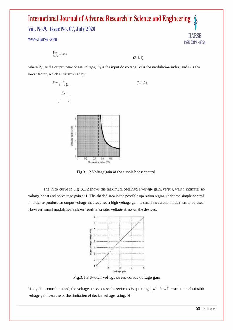
Fig.3.1.2 Voltage gain of the simple boost control
The thick curve in Fig. 3.1.2 shows the maximum obtainable voltage gain, versus, which indicates no
voltage boost and no voltage gain at 1. The shaded area is the possible operation region under the simple control.
In order to produce an output voltage that requires a high voltage gain, a small modulation index has to be used.
However, small modulation indexes result in greater voltage stress on the devices.
Fig.3.1.3 Switch voltage stress versus voltage gain
Using this control method, the voltage stress across the switches is quite high, which will restrict the obtainable
voltage gain because of the limitation of device voltage rating. [6]

60 | P a g e
3.2MAXIMUM BOOST CONTROL
We should maximize B for any given modulation index to achieve the maximum voltage gain.
Consequently, from (3.1.2), we have to make the shoot through duty ratio as large as possible.
Fig.3.2.1 maximum boost control waveform
Fig. 3.2.2 voltage gain of maximum boost control
Compared with the simple control method, shown in Fig. 3.1.3, the voltage stress in the proposed control method
is much lower, which means that for given devices, the inverter can be operated to obtain a higher voltage gain.

61 | P a g e
Fig. 3.2.3 Switch voltage stress versus voltage gain.
3.3MODIFIED PWM CONTROL FOR SHOOT THROUGH
From Fig. 3.3.1,the inverter with maximum constant boost control with third harmonic injection shoots
through twice in one cycle (triangular waveform cycle); the equivalent frequency to the inductor is doubled, thus
reducing the requirement to the inductors.
Fig.3.3.1 Maximum Constant Boost with Third Harmonic Injection
However, it is obvious from Fig. 3.3.1 that the real switching frequency of the device also doubles, which
increases the switching loss. In traditional PWM control, there is always a zero state after two active states, as
shown in Fig. 3.3.2. There are two types of zero states, Zero 1 and Zero 2, Zero 1 occurs when all upper three
switches are turned on, and Zero 2 occurs when all lower three switches are turned on. [8]
Fig. 3.3.2 Switching states sequence of traditional PWM control.
The control of the Z-source inverter maintains the active states unchanged and shoots through some or all of the
zero states. The key point of the modified PWM control is to turn half of the zero states (Zero 1 or Zero
2) into shoot-through state and leave the active states unchanged. The duty ratio of that shoot-through state equals
the shoot-through duty ratio of maximum constant boost control. [3]

62 | P a g e
2. HARMONIC COMPARISON BETWEEN VARIOUS CONTROL STRATEGIES
Sr
No
Type
of
conver
ter
Control
strategy
Fundamental
Harmonic order
3rd
5th
7th
9th
11th
13th
THD
1.
VSI
PWM control
397.5
4.715
11.25
10.33
4.729
10.65
10.32
0.9309
2.
ZSI
Simple boost
control
495.9
0.2915
7.224
2.017
0.374
1.068
1.606
0.9773
3.
ZSI
Third
harmonic
injection
476.5
138.9
22.05
12.49
8.38
2.818
1.672
1.1
Fig.4.1 Table of Harmonic Comparison for Various Control Strategies.
4.1SIMULATION MODEL
Fig. 4.1.1 shows complete simulation model in MATLAB SIMULINLK.
Fig.4.1.1 simulation model of Z source inverter with RL load.
63 | P a g e
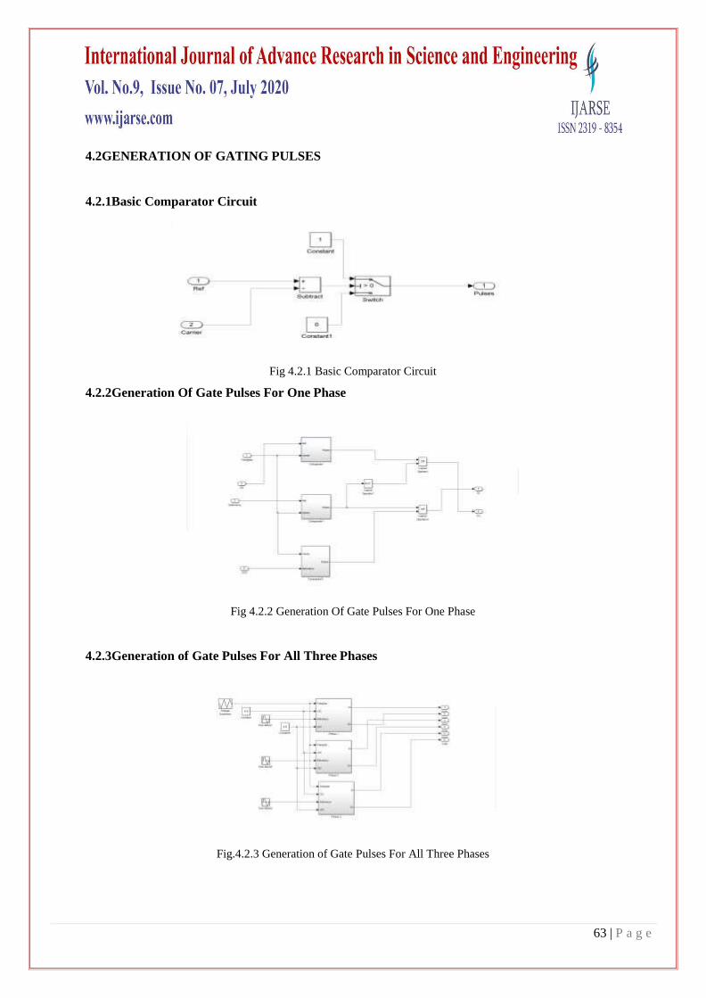
4.2GENERATION OF GATING PULSES
4.2.1Basic Comparator Circuit
Fig 4.2.1 Basic Comparator Circuit
4.2.2Generation Of Gate Pulses For One Phase
Fig 4.2.2 Generation Of Gate Pulses For One Phase
4.2.3Generation of Gate Pulses For All Three Phases
Fig.4.2.3 Generation of Gate Pulses For All Three Phases

64 | P a g e
3. CONCLUSIONS
A Z-Source Inverter is a buck boost inverter that has a wide range of obtainable value of output voltage,
which is verified through MATLAB/SIMULINK model. The various control strategies such as simple boost
control , maximum boost control and third harmonic injection control are studied and results are verified through
simulations and it is observed that third harmonic injection control method is more advantageous than other
methods. The performance of the scheme has been evaluated on the basis of THD & load voltage, load current
and found that the output voltage quality is good.
As per the results obtained from various simulations, following conclusions are obtained
1. For constant Z source inductance and modulation index, if Z source capacitance decreases then
output voltage increases.
2. For constant Z source capacitance and modulation index, if Z source inductance decreases then
output voltage increases.
3. For constant modulation index, if Z source capacitance and inductance decreases then output
voltage increases.
4. For constant Z source inductance & capacitance, if modulation index increases then output
voltage decreases.
5. For constant Z source capacitance and inductance if load resistance decreases then output voltage
decreases.
4. REFERENCE
[1] F. Z. Peng, “Z-source inverter,” IEEE Trans. Ind. Applicat., vol. 39, no.2, pp. 504–510, Mar./Apr. 2003.
[2] F. Z. Peng, X. Yuan, X. Fang, and Z. Qian, “Z-source inverter for adjustable speed drives,” IEEE Power
Lett., vol. 1, no. 2, pp. 33–35, Jun. 2003.
[3] D. A. Grant and J. A. Houldsworth, “PWM AC motor drive employing ultrasonic carrier,” in Proc.IEE
PE-VSD Conf., London, UK, 1984, pp.234–240
[4] K. Thorborg, Power Electronics. London, U.K.: Prentice-Hall International (U.K.) Ltd., 1988.
[5] M. H. Rashid, Power Electronics, 2nd ed. Englewood Cliffs, NJ Prentice-Hall, 1993.
[6] N. Mohan, W. P. Robbin, and T. Undeland, Power Electronics: Converters, Applications, and Design,
2nd ed. New York: Wiley, 1995.
A. M. Trzynadlowski, Introduction to Modern Power Electronics. New York: Wiley, 1998.

65 | P a g e
B. K. Bose, Modern Power Electronics and AC Drives. Upper Saddle River, NJ: Prentice-Hall PTR,
2002.
[7] P. T. Krein, Elements of Power Electronics. London, U.K.: OxfordUniv. Press, 1998.
[8] M. H. Rashid, Power Electronics, 2nd ed. Englewood Cliffs, NJ: Prentice-Hall, 1993.
[9] K. Thorborg, Power Electronics. London, U.K.: Prentice-Hall International (U.K.) Ltd., 1988.
[10] (IEEE Press Series on Power Engineering) Euzeli dos Santos, Edison R. da Silva-Advanced Power
Electronics Converters_ PWM Converters Processing AC Voltages-Wiley-IEEE Press (2014).
[11] Chaib Ibtissam, Behlouli Asma, Comparative study between different control strategy of the Z-Source
inverter.2017
[12] M. Z.Zizoui, B.Tabbache, F.Belkhiri , “Maximum Constant Boost Control of 9-Switch zSource Power Inverter-
Based Electric Vehicles”, The 5th International Conference on Electrical Engineering – Boumerdes (ICEE-B)
October 29-31, 2017, Boumerdes, Algeria.