Constant Voltage Source
26
Constant Voltage Source Gian Gentinetta December 16, 2019 Abstract In this experiment we aim to construct a constant voltage source. This is achieved using a full wave rectifier, Zener diodes, a buffer (including a transistor) and a constant current short circuit protection. This experiment was carried out in the constraints of the Physics Laboratory 3 at the Eidgenössische Technische Hochschule Zürich. Contents 1 Introduction 3 2 Setup 3 2.1 Preparations ................................... 3 2.2 Half Wave Rectifier ............................... 4 2.3 Full Wave Rectifier ............................... 4 2.4 Zener Diode ................................... 5 2.5 Side Task: Transistor .............................. 6 2.5.1 Current Amplification ......................... 6 2.5.2 Current Limit .............................. 6 2.5.3 Buffer .................................. 7 2.6 Buffered Zener Diode .............................. 7 2.7 Constant Current Source ............................ 7 2.8 Improved Power Supply ............................ 8 2.9 Integrated Circuit: LM7812 .......................... 9 2.10 Adjustable Voltage Stabilisation ........................ 9 3 Results 11 3.1 Preparations ................................... 11 3.2 Half Wave Rectifier ............................... 11 3.3 Full Wave Rectifier ............................... 12 3.4 Zener Diode ................................... 14 3.5 Transistor Side Tasks .............................. 14 1
-
Upload
khangminh22 -
Category
Documents
-
view
0 -
download
0
Transcript of Constant Voltage Source

Constant Voltage Source
Gian Gentinetta
December 16, 2019
Abstract
In this experiment we aim to construct a constant voltage source. This is achievedusing a full wave rectifier, Zener diodes, a buffer (including a transistor) and a constantcurrent short circuit protection. This experiment was carried out in the constraintsof the Physics Laboratory 3 at the Eidgenössische Technische Hochschule Zürich.
Contents1 Introduction 3
2 Setup 32.1 Preparations . . . . . . . . . . . . . . . . . . . . . . . . . . . . . . . . . . . 32.2 Half Wave Rectifier . . . . . . . . . . . . . . . . . . . . . . . . . . . . . . . 42.3 Full Wave Rectifier . . . . . . . . . . . . . . . . . . . . . . . . . . . . . . . 42.4 Zener Diode . . . . . . . . . . . . . . . . . . . . . . . . . . . . . . . . . . . 52.5 Side Task: Transistor . . . . . . . . . . . . . . . . . . . . . . . . . . . . . . 6
2.5.1 Current Amplification . . . . . . . . . . . . . . . . . . . . . . . . . 62.5.2 Current Limit . . . . . . . . . . . . . . . . . . . . . . . . . . . . . . 62.5.3 Buffer . . . . . . . . . . . . . . . . . . . . . . . . . . . . . . . . . . 7
2.6 Buffered Zener Diode . . . . . . . . . . . . . . . . . . . . . . . . . . . . . . 72.7 Constant Current Source . . . . . . . . . . . . . . . . . . . . . . . . . . . . 72.8 Improved Power Supply . . . . . . . . . . . . . . . . . . . . . . . . . . . . 82.9 Integrated Circuit: LM7812 . . . . . . . . . . . . . . . . . . . . . . . . . . 92.10 Adjustable Voltage Stabilisation . . . . . . . . . . . . . . . . . . . . . . . . 9
3 Results 113.1 Preparations . . . . . . . . . . . . . . . . . . . . . . . . . . . . . . . . . . . 113.2 Half Wave Rectifier . . . . . . . . . . . . . . . . . . . . . . . . . . . . . . . 113.3 Full Wave Rectifier . . . . . . . . . . . . . . . . . . . . . . . . . . . . . . . 123.4 Zener Diode . . . . . . . . . . . . . . . . . . . . . . . . . . . . . . . . . . . 143.5 Transistor Side Tasks . . . . . . . . . . . . . . . . . . . . . . . . . . . . . . 14
1

3.6 Buffered Zener Diode . . . . . . . . . . . . . . . . . . . . . . . . . . . . . . 153.7 Constant Current Source . . . . . . . . . . . . . . . . . . . . . . . . . . . . 163.8 Improved Power Supply . . . . . . . . . . . . . . . . . . . . . . . . . . . . 163.9 Integrated Circuits . . . . . . . . . . . . . . . . . . . . . . . . . . . . . . . 17
4 Analysis and Discussion 184.1 Input Voltage . . . . . . . . . . . . . . . . . . . . . . . . . . . . . . . . . . 184.2 Half and Full wave rectifiers . . . . . . . . . . . . . . . . . . . . . . . . . . 194.3 Zener Diode . . . . . . . . . . . . . . . . . . . . . . . . . . . . . . . . . . . 204.4 Transistor . . . . . . . . . . . . . . . . . . . . . . . . . . . . . . . . . . . . 214.5 Buffered Zener Diode . . . . . . . . . . . . . . . . . . . . . . . . . . . . . . 224.6 Constant Current Source . . . . . . . . . . . . . . . . . . . . . . . . . . . . 224.7 Improved Power Supply . . . . . . . . . . . . . . . . . . . . . . . . . . . . 234.8 Integrated Circuits . . . . . . . . . . . . . . . . . . . . . . . . . . . . . . . 24
5 Conclusion 26
References 26
2

Figure 1: The experimental setup of this laboratory session.
1 IntroductionThe goal of this experiment session is to build a constant voltage source. Here, constanthas two meanings: First, we construct a circuit that converts the AC-input source intoa DC-output. Secondly, we also aim to have an output voltage that is independent ofthe attached load. Constant voltage sources are essential in electronic devices which needDC-voltage to operate, as the voltage provided by the electronic power socket is usuallyAC. Having the voltage constant not only in time but also on changing the load helpsto have a reliable voltage source, which again is crucial for electronic devices to functionproperly. In this experiment we start with a simple diode to rectify the voltage and buildour way up to an advanced circuit with a reliable constant voltage source.
A secondary goal of the experiment is to receive a better understanding of the electroniccomponents used in the circuit. As part of this goal we examine with additional circuits,how transistors work and how they are characterized. Other components used in theexperiment are Zener diodes and (advanced) integrated circuit components.
2 Setup
2.1 Preparations
Before we start building the first circuit we familiarize ourself with the transformer providingthe input voltage and with the measurement tools (multimeter and oscilloscope). In all (butthe last few) circuits to come we use a short circuit protection resistance of R1 = 32Ω, whichprotects the transformer. To characterize the transformer we measure the voltage–currentcurve (UI-curve) of the input voltage. Measuring voltage, as well as the current, can bedone using the multimeter. In this first part we use the AC-setting of the multimeter whichshows the RMS value of the measured input. In addition, we can use the oscilloscope toplot the measured voltage as a function of time.
3

2.2 Half Wave Rectifier
In our first circuit (figure 2)we use a 1N4007 diode to suppress the current in one direction.We then use different capacitors C1 = 10µF , C2 = 100µF , C3 = 1000µF 1 to smooththe output voltage. For each capacitor we measure the UI-curve and the ripple voltageas a function of the load. To change the load on the output voltage we use (several)potentiometers.
Figure 2: Circuit including the Diode D1 as a half wave rectifier, as well as a capacitor C1
and short circuit protection R1.2
2.3 Full Wave Rectifier
The first improvement to our circuit is to replace the single diode with four diodes arrangedas shown in figure 3 to create a full wave rectifier. We perform the same measurements asin the last part for the same capacitors. In later experiments we replace the four separatediodes with a single piece B80R full wave rectifier.
1Important note: The capacitors used in this experiment are polarized, meaning that they have to beconnected to the circuit in the correct orientation. If this is done incorrectly the capacitor will most likelyexplode, as can be confirmed first hand by the author.
2The circuits shown in this report are taken from the manual on http://vp.phys.ethz.ch, 2019.
4

Figure 3: Circuit including a full wave rectifier B1, as well as a capacitor C1 and shortcircuit protection R1.
2.4 Zener Diode
Next, we add voltage stabilisation using a Zener diode (figure 4). Zener diodes have theproperty that they fix the output voltage if a properly biased current is applied in reversedirection. Using the information provided on the data sheet we calculate the followingresistances RZ to bias the diodes:
Diode Resistance RZ
C3V6 320 ΩC5V6 470 ΩC13 1k Ω
As smoothing capacitor we use from now on only C1 = 1000µF . Again we measure theUI-curve of the circuit to characterize the power supply.
Figure 4: Circuit including a full wave rectifier B1, a capacitor C1, short circuitprotection R1 and Zener diode stabilisation.
5
2.5 Side Task: Transistor
In this subsection of the experiment we build some separate circuits to develop an intuitionof how transistors work, so that we can later confidently use transistors in the main circuit.
2.5.1 Current Amplification
First, we want to observe the current amplification of the transistor. The circuit is shownin figure 5: We use a potentiometer to control the base current IB and measure how thecollector current IC depends on IB. As a our transistor we use the BD911 (n) part.
Figure 5: Circuit to measure the current amplification of a transistor.
2.5.2 Current Limit
As a next step we introduce an additional R1 resistance to the IC current (6) and performthe same measurements.
Figure 6: Circuit to measure the current amplification of a transistor with an additionalR1 resistance as current limit.
6

2.5.3 Buffer
We construct a voltage divider (figure 7) to control the voltage UB with a potentiometer.We then measure how UC depends on UB.
Figure 7: Buffer circuit: The voltage UB (controlled by a potentiometer) influences UC
through the transistor.
2.6 Buffered Zener Diode
Now that we know how to use transistors to create a buffer circuit we can implement abuffer to our main circuit. To prevent oscillations on the output voltage we additionallyadd a capacitor C2 = 1µF . The measurement of experiment 2.4 is repeated for the threediodes again with the same biasing resistances RZ .
Figure 8: Circuit including a full wave rectifier B1, a capacitor C1, short circuitprotection R1 and Zener diode stabilisation and a transistor as buffer.
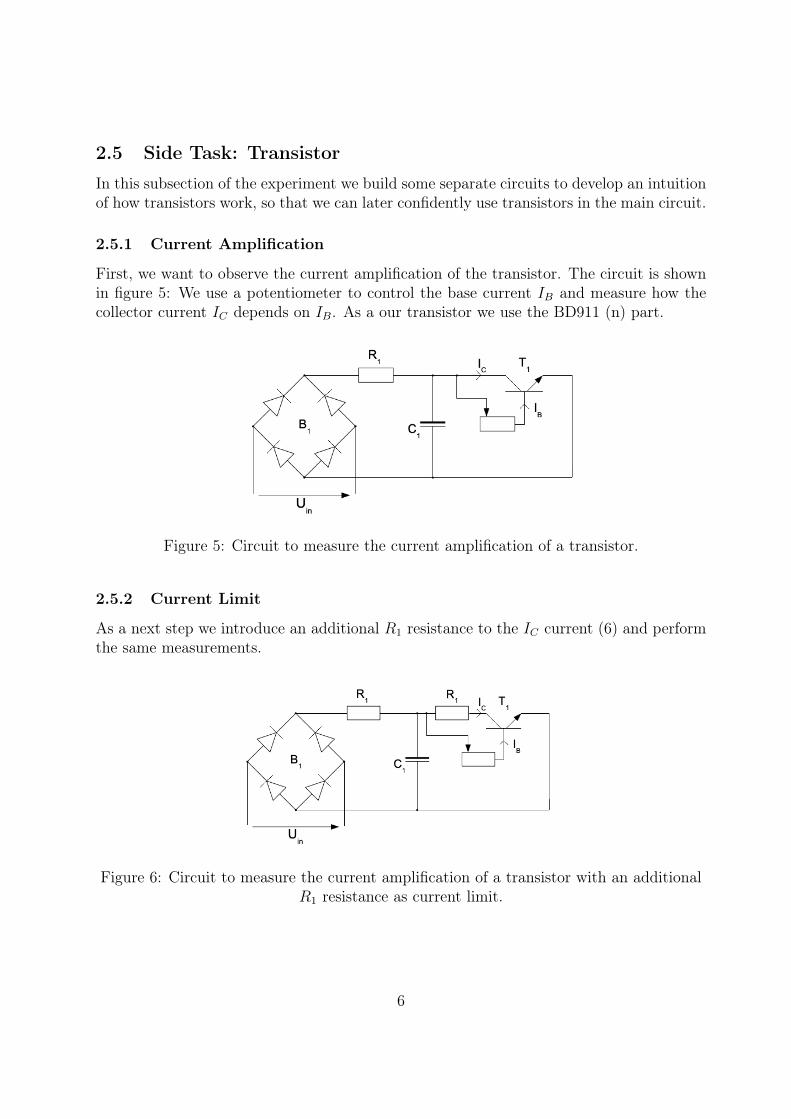
2.7 Constant Current Source
The next circuit (figure 9) is slightly more complex. The goal is to create a constantcurrent source (CCS) which can then be used to replace the short circuit resistance R1
7
(having the CCS makes sure the output current does not exceed a fixed maximal current).The circuit can be explained as follows: Once the output current I increases, the voltagedrop RSI on the shunt resistance increases and thus the base current IB decreases whichforces I to decrease over the transistor and vice versa. Using Ohm’s law we calculate theideal shunt resistance RS and biasing resistor R2 (the one connecting the Zener diode toground). Following the calculations we chose RS = 57Ω and R2 = 100Ω3 The Zener diodeused is the C5V6 model and the transistor is now a BD912 (p) type.
Again we measure the UI-curve of the system, this time with the goal of finding the currentas a function of the load.
Figure 9: Circuit providing a constant current source.
2.8 Improved Power Supply
As proposed earlier, we can now use the constant current source to replace our short-circuitprotection R1. This leads to the circuit shown in figure 10. We chose the 13 Volt diode C13as the diode controlling the output voltage with again RZ = 1kΩ. For the constant currentsource we still use the C5V6 diode but try out several shunt resistances (R1), namely 57 Ω,33 Ω and 47 Ω. The biasing resistance R2 is let constant at 100 Ω. The output UI-curveis then measured for the different R1 resistances.
3Note that this resistance differs from the previously used bias resistance. The circuit did not functionideally for the original R2 = 470Ω, thus, after experimenting with different values for R2 we found thatthe current was ideal for R2 = 100Ω.
8

Figure 10: Circuit including a full wave rectifier B1, a capacitor C1, constant currentsource and Zener diode stabilisation with a transistor as buffer.
2.9 Integrated Circuit: LM7812
We now simplify the above circuit by replacing the buffered Zener diode with a single pieceintegrated circuit LM7812 as shown in figure 11. Again we measure the UI-curve for thiscircuit.
Figure 11: Circuit including a full wave rectifier B1, a capacitor C1, constant currentsource and LM7812 regulator.
2.10 Adjustable Voltage Stabilisation
In the final circuit we replace the LM7812 with an LM317 piece. This allows to controlthe output voltage (which is normally set by the Zener diode used) with a potentiometer(figure 12). We measure the UI-curves for 3 output ranges (approximately 13, 5 and 3.5Volts).
9

Figure 12: Circuit including a full wave rectifier B1, a capacitor C1, constant currentsource and LM317 variable regulator.
10

(a) C1 = 10µF (b) C1 = 100µF (c) C1 = 1000µF
Figure 14: UI-curve of the half wave rectifier for different capacitors C1.
3 Results
3.1 Preparations
The UI-curve of the transformer (with short circuit protection) is shown in figure 13. Theerror propagation in this and the following plots was done using the uncertainties pythonpackage [1].
Figure 13: UI-curve of transformer with short circuit protection R1.
3.2 Half Wave Rectifier
For the half wave rectifier we measured the UI-curves for the different capacitors (figure14). Additionally, figure 15 provides snapshots of the input and output voltages measuredwith the oscilloscope for the different capacitors to show the ripple voltage. Figure 16shows the ripple voltage as a function of the load.
11

(a) C1 = 10µF (b) C1 = 100µF (c) C1 = 1000µF
Figure 15: Measured input and output voltages for the half wave rectifier for differentcapacitors C1.
Figure 16: Ripple voltage of the half wave rectifier as a function of the load for thedifferent capacitors.
3.3 Full Wave Rectifier
The same measurements were performed for the full wave rectifier. The UI-curves arefound in figure 17, the output voltage in figure 18 and the ripple voltage as a function ofthe load in figure 19
12

(a) C1 = 10µF (b) C1 = 100µF (c) C1 = 1000µF
Figure 17: UI-curve of the full wave rectifier for different capacitors C1.
(a) C1 = 10µF (b) C1 = 100µF (c) C1 = 1000µF
Figure 18: Measured output voltages for the full wave rectifier for different capacitors C1.
13

Figure 19: Ripple voltage of the full wave rectifier as a function of the load for thedifferent capacitors.
3.4 Zener Diode
Figure 20 shows the UI-curves of the different Zener diodes.
Figure 20: UI-curves for the circuits with the Zener diode voltage stabilisation.
3.5 Transistor Side Tasks
Figure 21 shows the dependence IC(IB), with and without current limit (additional R1).Figure 22 shows the dependence UC(UB) for the circuit in figure 7.
14

(a) Total region (b) Linear region
Figure 21: Current amplification with the transistor. Shows collector current IC as afunction of the base current IB with and without current limit.
Figure 22: Voltage follower: Shows how changing the voltage UB controls the voltage UC
in the circuit in figure 7.
3.6 Buffered Zener Diode
Figure 23 shows the UI-curves of the circuit in figure 8 (buffered Zener diode) for thedifferent Zener diodes.
15

Figure 23: UI-curves for the circuits with the Zener diode voltage stabilisation andtransistor as buffer.
3.7 Constant Current Source
For this experiment, we are interested in how the current changes as a function of thevoltage. This is why in figure 24 the current is shown on the vertical axis with the voltageon the horizontal.
Figure 24: Showing the current as a function of the output voltage for the constantcurrent source experiment.
3.8 Improved Power Supply
In this part it is all coming together. The UI-curve of the circuit in figure 10 is shown infigure 25.
16

Figure 25: UI-curves for the circuit with the Zener diode voltage stabilisation andtransistor as buffer and constant current source as active short circuit protection, for
different shunt resistances R1.
3.9 Integrated Circuits
The final UI-curves are given in figures 26 and 27 for the LM7812 and LM317 integratedcircuits, respectively. For the LM317 piece the curves are given for three different loads onthe voltage divider.
Figure 26: UI-curve for the circuit with the LM7812 integrated circuit.
17

Figure 27: UI-curves for the circuit with the LM217 integrated circuit, for 3 differentvoltage ranges.
4 Analysis and DiscussionIn this section we will discuss the measured UI-curves and analyse how the circuit improvedover the several iterations. Additionally, we calculate the output impedance of the circuits,using the following formula:
Rimp =Umax − Uout
Iout(1)
where Umax = 18.5 V is the maximal voltage measured in the very first experiment(UI-curve of the transformer). The impedance is not bound to be constant, thus, wewill look at the dependence Rimp(Iout).
4.1 Input Voltage
As expected, the UI-curve of the transformer is linear, following Ohm’s law. For thisfirst experiment we subtracted the short circuit protection R1 from Rimp to receive theactual impedance of the transformer. This is shown in figure 28. It is to be noticed thatthe impedance is not constant for different loads and the higher the load the higher theimpedance.
18
Figure 28: Output impedance of the transformer.
4.2 Half and Full wave rectifiers
The important data taken in this experiment are the screenshots of the oscilloscope. Theyhelp to analyse how the different capacitors affect the ripple voltage. It can easily be seenthat the highest capacitance (1000 µF) provides the most constant output voltage, i.e. thesmallest ripple. This is reasonable, as the higher capacitance allows to store more electricalcharge which leads to a better smoothing of the output voltage. This explains why fromhere on we always used the 1000 µF capacitor. Here we can also see that the half waverectifier clearly just blocks the negative voltage, while the full wave rectifier provides asignal, which is again roughly sinusodial, just with a much smaller amplitude than theinput voltage.
We can also analyse how the ripple changes for different loads. Theoretically, the ripplevoltage is predicted to be approximately
Uripple ≈IoutfC1
(2)
for the half wave rectifier andUripple ≈
Iout2fC1
(3)
for the full wave rectifier. This linear behaviour can be observed only in a very limitedcurrent range. Nevertheless, the approximation is shown as a fit in figure 29. Particularlyfor the 10µF capacitor the prediction line does not fit the measured data at all. Thispossibly could have been improved by using larger potentiometers to measure the ripplefor lower currents. From the ripple-current plots we can also deduce that the full wave
19

(a) Half wave rectifier (b) Full wave rectifier
Figure 29: Ripple voltages of the half and full wave rectifiers as a function of the load.The grey lines indicate the predicted values according to equations 2 and 3.
rectifier does indeed produce a lower ripple. Especially for the two larger capacitors theripple is approximately half in size (as predicted by the given formulas).
Considering the UI-curve, there is not much to be discussed in this subsection, as thesecircuits are not (yet) built to have the output voltage constant for changing currents. It,thus, does not come unexpected that the UI-curves look more ore less equal to the originalUI-curve. Figure 30 shows the output impedance for the two circuits. It seems that forthe higher capacitors the impedance increases with the current until reaching a limit of100 Ω for the half wave rectifier and 50 Ω for the full wave rectifier. Again, the 10µFcapacitor does not fit the behaviour of the larger capacitors. This anomaly could possiblybe explained as the output voltage of the smallest capacitor is nowhere near constant intime (compared to the other capacitors, as seen in figures 15 and 18) which can lead tounexpected behaviour.
4.3 Zener Diode
Finally, we see some improvements in the UI-curve. As predicted, the Zener diode fixesthe output voltage at a fixed value, which approximately coincides with the value providedon the data sheet (13V, 5.6V and 3.6V). It is, however, to be noted that the voltage onlystays constant for a very limited current range. The voltage then starts dropping again atabout 7 mA, 30 mA and 50 mA for the C13, C5V6 and C3V6 diodes, respectively. Fromthis plot it seems that the C5V6 diode has the most constant voltage (in the range whereit is constant), while the C3V6 diode has a broader current range, where the voltage isapproximately constant. So if high currents are needed, one should use the C3V6 diode, butif the current stays below 30 mA, the C5V6 diode seems to provide the most reliable output.
20

(a) Half wave rectifier (b) Full wave rectifier
Figure 30: Output impedance of the half and full wave rectifier, calculated using equation1, for the different capacitors.
The output impedance is shown in figure 31. In the useful range (where the voltage isapproximately constant), the impedance seems to be inverse proportional to the current.On first sight, it seems as if the C13 diode behaves unexpectedly, but it is to be noted thatonly 3 measurement points were taken in the useful range for this diode. While the circuitdid improve the constant voltage source, it did massively increase the output impedance.Even in the final range the impedance does not sink below 400 Ω, which of course leads toa power loss in the circuit.
4.4 Transistor
As this is a side task, we will only briefly discuss the plots in figure 21 and 22. The first plotconfirms the linear dependence IC(IB) for small currents IB. When the resistance in thepotentiometer becomes low (and thus IB large), the current starts flowing via Base-Emittorin stead of Collector-Emittor, which makes the IC current constant. Adding an additionalresistor R1 to the circuit limits the collector current to approximately 230 mA. This isbecause the R1 increases the resistance on the collector and thus the IC current will becomeconstant earlier (i.e. for smaller base current IB).
The second figure shows that the voltage UE depends linearly on UB. As a consequence,we can control the output voltage by changing UB. As there is almost no load on UB, thereis a minimal power loss in this voltage-control.
21

Figure 31: Output impedance of the different Zener diodes.
4.5 Buffered Zener Diode
From the UI-curve in figure 23 we directly see the effect of adding the transistor as a buffer.The current range, in which the voltage stays constant has been massively increased toapproximately 100 mA, 230 mA, 300mA for the C13, C5V6 and C3V6 diodes, respectively.Again, the C5V6 diode has the most stable output voltage, whereas the C3V6 diode hasthe widest current range for the constant voltage output. The C13 diode still has the mostlimited current range and in addition behaves unstable for currents I < 50 mA.
Figure 32 shows the output impedance for the different diodes. Again, the impedanceseems to be inversely proportional to the output current. Note that in this plot onlythe data for currents larger than 3 mA are displayed, as the impedance values for smallercurrents become so large that the scale of the plot would remove all information concerningthe values for larger currents. Compared to the Zener diode without the buffer there is alarge improvement in the power supply. The impedance reaches a minimum of 55 ± 5 Ωfor all three diodes, which undercuts the impedance of the previous circuit by an order ofmagnitude.
4.6 Constant Current Source
We will now analyse the constant current source. The initial goal was to have an outputcurrent of approximately 100 mA. Using Ohm’s law we calculated the shunt resistance RS
needed to achieve this value:
R1 ≈UZ − UBE
IC≈ 5.6V − 0.6V
100mA= 50Ω (4)
22

Figure 32: Output impedance of the different Zener diodes for the buffered Zener diodecircuit.
In the experiment we later used R1 = 57Ω which lead to the slightly lower current ofapproximately 88 mA. As shown in figure 24 the current stays constant as expected forvoltages below 7V. At that point the resistance on I becomes too large and the currentsource becomes saturated, leading to a decreasing current I.
4.7 Improved Power Supply
In this experiment we had to chose 2 Zener diodes: One to control the constant currentsource and another to set the output voltage. We chose the C5V6 diode for the currentsource, as it provides the most stable constant voltage, for the constant current sourcepart. For the output voltage we chose the C13 diode because it’s UI-curve had the highestpotential for possible improvements.
In figure 33 we compare the C13 diode without constant current source with the threedifferent constant currents in figure 25. First, we realise that the strange behaviour forsmall currents has been fixed – the voltage is now more stable in the constant range.Secondly, we find that the constant current source works perfectly: It hinders the outputcurrent from becoming too large. We can, thus, use the constant current source to cut offthe output voltage completely at the point where the current becomes too large for theconstant voltage source anyway. Analysing the different curves we see that this sweet spotwould be for a shunt resistance somewhere between 47 and 57 Ω.
Looking at the output impedance shown in figure 34 we see that it did not changesignificantly compared to the previous circuit. This is because the impedance of theprevious passive short circuit protection was negligible compared to the impedance ofthe remaining circuit for smaller currents. For currents of 100 mA and larger we start to
23

Figure 33: UI-curves for the the buffered C13 Zener diode. Comparing the differentconstant current sources with the initial passive short circuit protection.
see a slight difference in the impedance and it seems like the active short circuit protectionusing the constant current source is indeed more effective than the passive short circuitprotection.
4.8 Integrated Circuits
Finally, we will compare the two integrated circuits LM7812 and LM317 to the previouscircuits. Figure 35 compares the LM7812 circuit with the previous circuit, where theconstant current source is set at R1 = 47Ω for both circuits. It can be seen that the newcircuit is slightly more stable than the buffered Zener diode: While the voltage is slowlysinking with increasing current for the Zener diode, it stays perfectly constant for theintegrated circuit.
The same improvements can be seen with the LM317 piece. This circuit has the additionaladvantage of the adjustable output voltage. Considering the output impedance of theintegrated circuits, there is not a significant improvement to the buffered Zener diode, ascan be seen in figure 36. It is also to be noted that the the impedance is larger if theoutput voltage is set at a higher fix point meaning that the circuit is more effective forhigher output voltages.
24

Figure 34: Output impedance for the the buffered C13 Zener diode. Comparing thedifferent constant current sources with the initial passive short circuit protection.
Figure 35: UI-curve of the circuit containing the LM7812 integrated circuit compared tothe buffered Zener C13 diode.
25

(a) LM7812 (b) LM317
Figure 36: Output impedance of final circuit including the integrated circuit parts,compared to the buffered Zener diode C13.
5 ConclusionWe consider this experiment session a success. The first goal of having an output voltagethat is constant in time (DC) was already achieved to a satisfying degree with the circuitcontaining a full wave rectifier. From this stage on we continuously extended the circuit towork towards our second goal, which was to have an output voltage that does not dependon the output current (and, thus, on the load). With every step the UI-curve improveduntil we achieved our goal with the buffered Zener diode powered by a constant currentsource. More importantly we improved our understanding of the components used in theconstructed circuits and developed an intuition off their functionality.
References[1] Uncertainties: a Python package for calculations with uncertainties, Eric O. LEBIGOT,
http://pythonhosted.org/uncertainties/.
26