
DC-Voltage-Ratio Control Strategy for Multilevel Cascaded Converters Fed With a Single DC Source
Upload
independentCategory
view
0download
0
4
2 SPACE VECTOR MODULATION FOR THREE-LEG VOLTAGE
SOURCE INVERTERS
2.1 THREE-LEG VOLTAGE SOURCE INVERTER
The topology of a three-leg voltage source inverter is shown in Fig. 2.1. Because
of the constraint that the input lines must never be shorted and the output current must
always be continuous a voltage source inverter can assume only eight distinct topologies.
These topologies are shown on Fig. 2.2. Six out of these eight topologies produce a non-
zero output voltage and are known as non-zero switching states and the remaining two
topologies produce zero output voltage and are known as zero switching states.
Fig. 2.1. Topology of a three-leg voltage source inverter.
L
p
n
ab
c
A
CB
Ia
Vg

5
p
ab
c
n V2(ppn)
p
ab c
n V3(npn)
p
ab c
n V4(npp)
ab c
n V1(pnn)
p
ab c
n V5(nnp)
p
ab c
n V7(ppp)
p
ab c
n V6(pnp)
p
ab c
n V8(nnn)
p
Fig. 2.2. Eight switching state topologies of a voltage source inverter.
2.2 VOLTAGE SPACE VECTORS
Space vector modulation (SVM) for three-leg VSI is based on the representation
of the three phase quantities as vectors in a two-dimensional (α β, ) plane. This has been
discussed in [1] and is illustrated here for the sake of completeness. Considering
topology 1 of Fig. 2.2, which is repeated in Fig. 2.3 (a) we see that the line voltages Vab,
Vbc, and Vca are given by
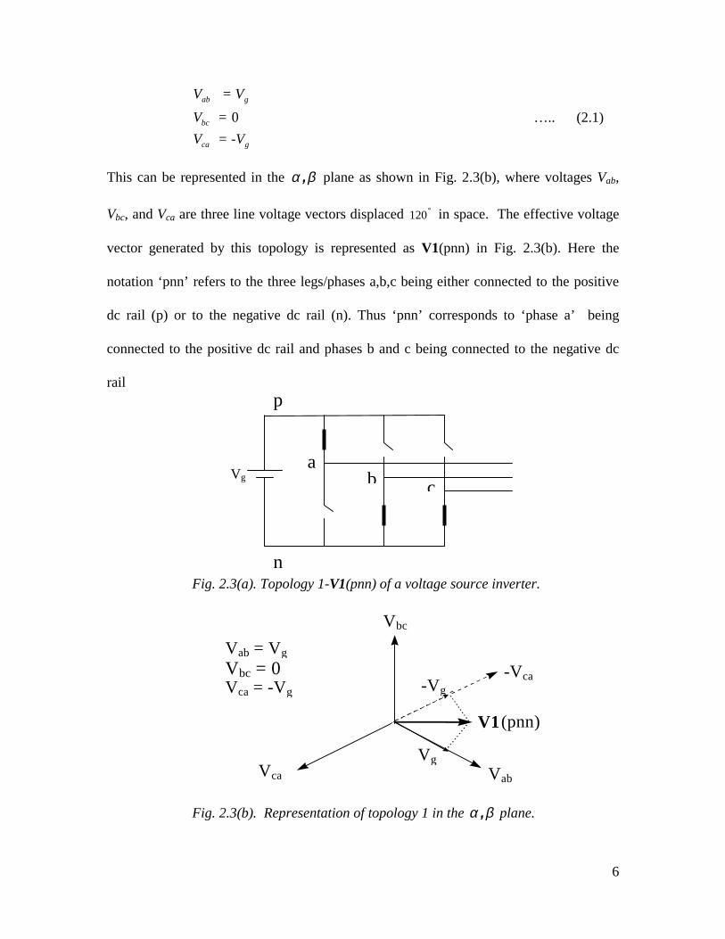
6
a
n
cbVg
p
gca
bc
gab
= -VV
= V
= VV
0 ….. (2.1)
This can be represented in the α β, plane as shown in Fig. 2.3(b), where voltages Vab,
Vbc, and Vca are three line voltage vectors displaced 120° in space. The effective voltage
vector generated by this topology is represented as V1(pnn) in Fig. 2.3(b). Here the
notation ‘pnn’ refers to the three legs/phases a,b,c being either connected to the positive
dc rail (p) or to the negative dc rail (n). Thus ‘pnn’ corresponds to ‘phase a’ being
connected to the positive dc rail and phases b and c being connected to the negative dc
rail
Fig. 2.3(a). Topology 1-V1(pnn) of a voltage source inverter.
Vab
Vbc
Vca
-Vca
Vg
-Vg
V1(pnn)
Vab = Vg
Vbc = 0Vca = -Vg
Fig. 2.3(b). Representation of topology 1 in the α β, plane.

7
Proceeding on similar lines the six non-zero voltage vectors (V1 - V6) can be
shown to assume the positions shown in Fig.2.4. The tips of these vectors form a regular
hexagon (dotted line in Fig. 2.4). We define the area enclosed by two adjacent vectors,
within the hexagon, as a sector. Thus there are six sectors numbered 1 - 6 in Fig. 2.4.
V1
V2V3
V4
V5 V6
12
3
45
6
Fig. 2.4. Non-zero voltage vectors in the α β, plane.
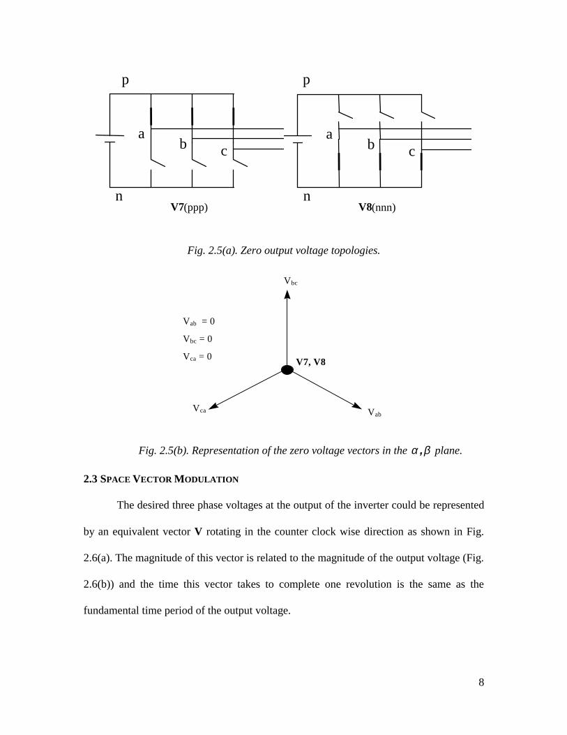
Considering the last two topologies of Fig. 2.2 which are repeated in Fig. 2.5(a)
for the sake of convenience we see that the output line voltages generated by this
topology are given by
0
0
0
===
ca
bc
ab
V
V
V
….. (2.2)
These are represented as vectors which have zero magnitude and hence are
referred to as zero-switching state vectors or zero voltage vectors. They assume the
position at origin in the α β, plane as shown in Fig. 2.5(b). The vectors V1-V8 are called
the switching state vectors (SSVs).
8
ab c
n V7(ppp)
p
ab c
n V8(nnn)
p
Fig. 2.5(a). Zero output voltage topologies.
Vab
Vbc
Vca
V7, V8
Vab = 0
Vbc = 0
Vca = 0
Fig. 2.5(b). Representation of the zero voltage vectors in the α β, plane.
2.3 SPACE VECTOR MODULATION
The desired three phase voltages at the output of the inverter could be represented
by an equivalent vector V rotating in the counter clock wise direction as shown in Fig.
2.6(a). The magnitude of this vector is related to the magnitude of the output voltage (Fig.
2.6(b)) and the time this vector takes to complete one revolution is the same as the
fundamental time period of the output voltage.

9
V1
V2V3
V4
V5 V6
1
2
3
4
5
6
V
Vab
Vbc
Vca
Fig. 2.6(a). Output voltage vector in the α β, plane.
1 2 3 4 5 6
V ab V bc V caV
0
Fig. 2.6(b). Output line voltages in time domain.
Let us consider the situation when the desired line-to-line output voltage vector V
is in sector 1 as shown in Fig. 2.7. This vector could be synthesized by the pulse-width-
modulation (PWM) of the two adjacent SSV’s V1(pnn) and V2 (ppn), the duty cycle of
each being d1 and d2, respectively, and the zero vector ( V7(nnn) / V8(ppp) ) of duty
cycle d0 [1]:
jèg e = m V = + d d VVV 21 21 ….. (2.3)
1021 = + d+ d d ….. (2.4)
where, 86600 . m ≤≤ , is the modulation index. This would correspond to a maximum
line-to-line voltage of 1.0Vg, which is 15% more than conventional sinusoidal PWM as
shown [1].

10
d1 V1(pnn)
V2(ppn)
1Vd2
V7(ppp)
V8(nnn)
θ
Fig. 2.7. Synthesis of the required output voltage vector in sector 1.
All SVM schemes and most of the other PWM algorithms [1,4], use (2.3), (2.4)
for the output voltage synthesis. The modulation algorithms that use non-adjacent SSV’s
have been shown to produce higher THD and/or switching losses and are not analyzed
here, although some of them, e.g. hysteresis, can be very simple to implement and can
provide faster transient response. The duty cycles d1, d2, and d0, are uniquely determined
from Fig. 2.7, and (2.3), (2.4), the only difference between PWM schemes that use
adjacent vectors is the choice of the zero vector(s) and the sequence in which the vectors
are applied within the switching cycle.
The degrees of freedom we have in the choice of a given modulation algorithm
are:
1) The choice of the zero vector -
whether we would like to use V7(ppp) or V8(nnn) or both,
2) Sequencing of the vectors
3) Splitting of the duty cycles of the vectors without introducing additional
commutations.
Four such SVM algorithms are considered in the next section, namely:
1) The right aligned sequence ( SVM1)

11
2) The symmetric sequence (SVM2)
3) The alternating zero vector sequence ( SVM3)
4) The highest current not switched sequence (SVM4) .
The modulation schemes are described for the case when the reference vector is in
sector 1: all other cases are circularly symmetric.
These modulation schemes are analyzed and their relative performance with
respect to switching loss, THD and the peak-to-peak current ripple at the output is
assessed. The analysis is performed over the entire range of modulation index and for
load power factor angle varying from –90o to 90o.
All space vector modulation schemes presented here assume digital
implementation and, hence, regular sampling, i.e. all duty cycles are precalculated at the
beginning of the switching cycle, based on the value of the reference voltage vector at
that instant.
2.4 MODULATION SCHEMES
2.4.1 RIGHT ALIGNED SEQUENCE (SVM1)
A simple way to synthesize the output voltage vector is to turn-on all the bottom
(or top) switches at the beginning of switching cycle and then to turn them off
sequentially so that the zero vector is split between V7(ppp) and V8(nnn) equally. This
switching scheme is shown in Fig. 2.8 for two sampling periods. The signals in the figure
represent the gating signals to the upper legs of the inverter. The scheme has three switch
turn-on’s and three switch turn-off’s within a switching cycle. The performance of the left
aligned sequence, where the sequence of vectors is exactly opposite to the right aligned
sequence, is expected to be similar to the right aligned sequence.
12
nnn pnn ppn ppp
T s
d0/2 d1 d2 d0/2
nnn pnn ppn ppp
T s
d0/2 d1 d2 d0/2
a
b
c
pn
pn
pn
Fig. 2.8. Phase gating signals in SVM1.
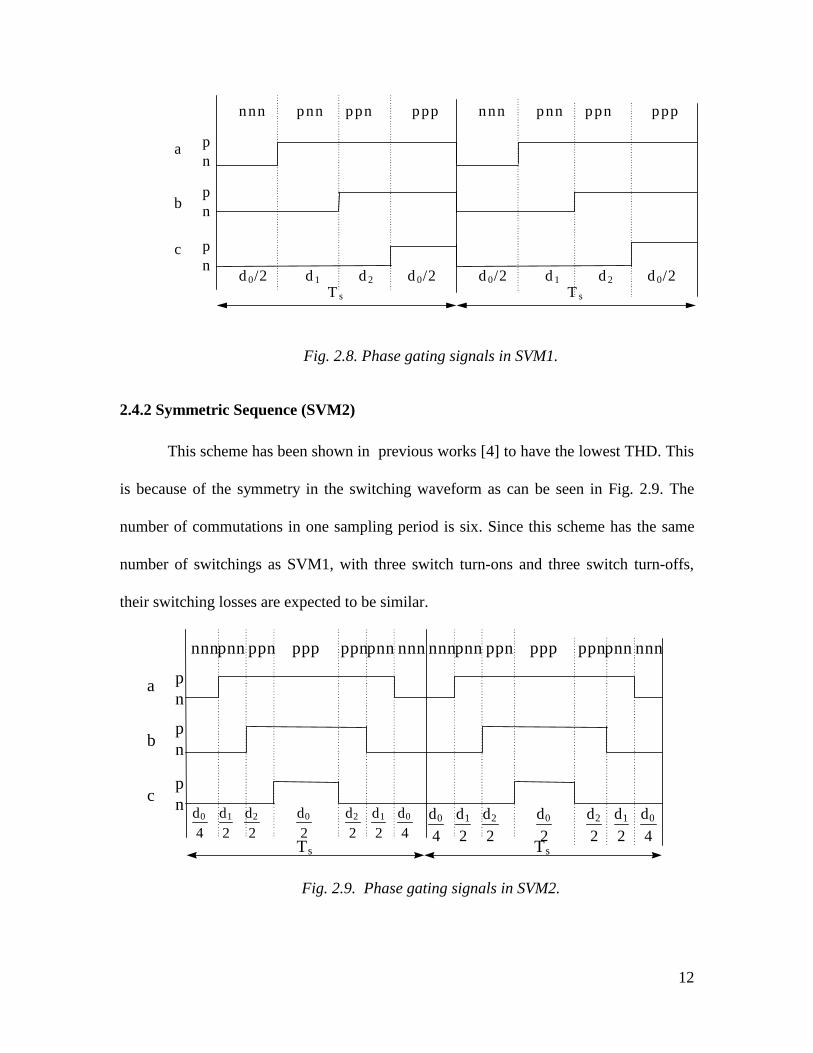
2.4.2 Symmetric Sequence (SVM2)
This scheme has been shown in previous works [4] to have the lowest THD. This
is because of the symmetry in the switching waveform as can be seen in Fig. 2.9. The
number of commutations in one sampling period is six. Since this scheme has the same
number of switchings as SVM1, with three switch turn-ons and three switch turn-offs,
their switching losses are expected to be similar.
Ts
pnn ppn ppp ppnpnnnnn nnn
Ts
pnn ppn ppp ppnpnnnnn nnn
d0
4d1
2d2
2d0
2d2
2d1
2d0
4d0
4
d1
2
d2
2
d0
2
d2
2
d1
2
d0
4
a
b
c
pn
pn
pn
Fig. 2.9. Phase gating signals in SVM2.

13
2.4.3 Alternating Zero Vector Sequence (SVM3)
In this scheme, known as DI sequence in literature [6], the zero vectors V7(ppp)
and V8(nnn) are used alternatively in adjacent cycles so that the effective switching
frequency is halved, as shown in Fig. 2.10.
T s
pnn ppn ppp
d1 d2 d0
ppn pnn nnn
d2 d1 d0T s
a
b
c
pn
pn
pn
Fig. 2.10. Phase gating signals in SVM3.
However, the sampling period is still Ts, same as in the other schemes. The switching
losses for this scheme are expected to be ideally 50% as compared to those of the
previous two schemes and THD significantly higher due to the existence of the harmonics
at half of the sampling frequency.
2.4.4 Highest Current Not-Switched Sequence (SVM4)
This scheme, known as DD sequence in literature [6], is based on the fact that the
switching losses are approximately proportional to the magnitude of the current being
switched and hence it would be advantageous to avoid switching the inverter leg carrying
the highest instantaneous current. This is possible in most cases, because all adjacent
SSV’s differ in the state of switches in only one leg. Hence, by using only one zero
vector, V7(ppp) or V8(nnn) within a given sector one of the legs does not have to be
switched at all, as shown in Fig. 2.11 (a).

14
Ts
ppppnn ppn
d1 d2 d0Ts
ppppnn ppn
d1 d2 d0
a
b
c
pn
pn
pn
Fig. 2.11(a). Phase gating signals in SVM4.
However, since the choice of the non-zero SSVs is based on the desired output
voltage vector and the phase and magnitude of the current are determined by the load, it
is not always possible to avoid switching the phase carrying the highest current. In such a
case the phase carrying the second highest current is not switched and the switching
losses are still reduced. For example, the choice of zero vectors in sector 1 is determined
using the flowchart in Fig. 2.11(b).
|Ia| > |Ic| d0 V7(ppp)
d0 V8(nnn)
Y
N
Fig. 2.11(b). Choice of zero vector in sector 1.
2.5 ANALYSIS
In this section the THD, switching losses and peak-to-peak current ripple of all the
schemes are analyzed over the entire range of modulation index, and over varying load
power factor angles.

15
2.5.1 Total Harmonic Distortion
The total harmonic distortion (THD) of a periodic voltage which can be
represented by the Fourier series tjnneVV ω∑
∞
=1 =n
is defined as
1
2
2
= V
V
THD nn∑
∞
= ….. (2.5)
and its weighted total harmonic distortion is defined as
1
2
2 =
V
n
V
WTHD
n
n
∑∞
= ….. (2.6)
The analysis of THD is done based on a novel algorithm where the Fourier
coefficients of all the pulses of a given line/phase voltage in one fundamental time period
are summed up. The analysis is valid for all integral fs/fo, where fs is the switching
frequency and fo is the fundamental frequency at the output of the inverter.
Fig. 2.12 shows the plot of typical phase voltage in one fundamental time period.
The THD of this waveform is calculated by first decomposing the waveform of Fig. 2.12
into a series is pulses which resemble Fig. 2.13.
To
Ts
Ph
ase
Vo
ltag
e
Time
Fig. 2.12. Typical Phase voltage in one fundamental time period.
Pha
se V
olta
ge
Time

16
Then the Fourier components for each of these pulses are calculated and summed up to
get the effective Fourier components of the entire waveform in one fundamental time
period. This procedure is illustrated here for SVM1.
Considering a pulse shown in Fig. 2.13 with fundamental period To = 1/fo (Fig.
2.12) its Fourier coefficients at frequency nfo are given by
) ) 2
( sin ) ) ( 2
( sin ( o
mmsm
o
mn
T
TnTTd
T
n
n
Va
πππ
−+= ….. (2.7)
) ) ) ( 2
( cos ) 2
( cos ( msmoo
mmn TTd
T
n
T
Tn
n
Vb +−= ππ
π….. (2.8)
Tm d Tm s
Vm
Ts
Fig. 2.13. Output voltage pulse.
where dm is the pulse duty cycle, Tm is the pulse delay time, Vm is the pulse
magnitude, and s
s f = T
1, is the sampling time period.
Decomposition of the phase voltage switching waveform for SVM1 (Fig. 2.13) to
obtain a series of pulses as in Fig. 2.12 is a two step process. At first the waveform is
decomposed to obtain stepped pulses as shown in Fig. 2.14(a), then this stepped pulse
waveform is further decomposed to obtain pulses, similar to Fig. 2.13, as shown in Fig.
2.14(b) and Fig. 2.14(c).
Time
Vo
ltage

17
Consider the load to be wye connected and balanced. Then the phase voltages Va,
Vb Vc with respect to a neutral point (N) chosen such that Va+Vb+Vc=0 in any sector for
any load can be obtained from 333
bccac
abbcb
caaba
- VV = , V
- VV = , V
- VV = V
The phase voltage (Va) in sector1 during different SSVs (V8,V1,V2,V7) for
SVM1 is shown in Table 2.1
Table 2.1. Phase voltage in sector 1: SVM1.
SSV’s V8(nnn) V1(pnn) V2(ppn) V7(ppp)duty cycle d0/2 d1 d2 d0/2
Va 0 2Vg/3 Vg/3 0
Fig. 2.14 shows the decomposition of a typical phase voltage in the kth switching
interval from the beginning of the phase voltage period, where
10 - f
f k
o
s≤≤ ….. (2.9)
d0/2 d1 d2 d0/2
2Vg/3
Vg/3
d0/2 d1 d0/2+d2
2Vg/3
Vg/3
d0/2+d1 d2 d0/2
(k-1)Ts kTs (k-1)Ts kTs kTs(k-1)Ts
0 0 0
(a) (b) (c)
Fig. 2.14. Phase voltage decomposition in one sampling period.
Comparing each of the component pulses with Fig. 2.13 one can find that for the
first pulse

18
,3
2
21 0
1
gm
smm
V = V
, Td
+ k - = , T= dd
….. (2.10)
and for the second pulse
3
12
012
Vg = V
, T + dd
+ k - = , T = dd
m
sm m
….. (2.11)
The duty cycles d1, d2 and d0 are calculated using (2.3) and (2.4). The Fourier
components of these pulses are obtained from (2.7) and (2.8). Thus the Fourier
coefficients of the phase voltage can be found using:
∑∑==
+=1 -
0
2
1 -
0
2o
s
o
s
f
f
kk
f
f
kkn baV ….. (2.12)
The Fourier coefficients of the line current can be obtained by
n
n
currentlinen z
VI =_ ….. (2.13)
where nz is the impedance of a given phase.
Alternatively, WTHD of line voltage could represent a THD of line current [2,3].
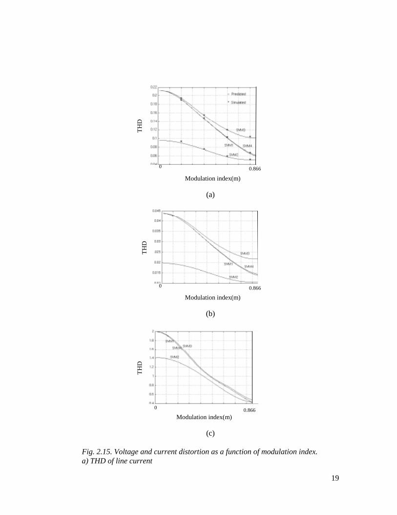
Fig. 2.15 shows the THD of the simulated line current and line voltage and the WTHD of
line voltage for all the schemes over the entire range of modulation index, for the inverter
parameters Vg = 400V, fo = 60 Hz, fs = 2160, R(load) = 3, L(load) = 1mH. Appendix B
lists the MATLAB code, used to generate the ‘predicted’ results in Fig. 2.15.
19
0 0.866
0 0.866
0 0.866
Modulation index(m)
(a)
Modulation index(m)
(b)
Modulation index(m)
(c)
Fig. 2.15. Voltage and current distortion as a function of modulation index.a) THD of line current
TH
DT
HD
TH
DT
HD

20
b) WTHD of line currentc) THD of line voltage
These results agree with what is found in literature. It is interesting to note that the
THD (line current and voltage) for all the schemes decreases with increase in modulation
index. This is because of the increase in the fundamental component of the
voltage/current with increase in modulation index; the other higher order harmonics being
relatively constant. It can also be seen that SVM2 (symmetic) has the least THD. This
can be associated with the symmetry in the switching waveform. By introducing
symmetry (SVM2), the number of phase voltage pulses in a given switching time-period
is doubled as compared to the other schemes. This would make the converter look as if it
were operating at twice the switching frequency. Hence this results in a reduced THD
and reduced peak-to-peak ripple in the load current.
2.5.2. Switching Losses
The switching losses are assumed to be proportional to the product of the voltage
across the switch and the current through the switch at the instant of switching. Since the
voltage across the switch is the bus voltage, it is considered to be a constant. Thus the
losses are proportional to the current during switching.
As a first approximation, the switching ripple is neglected and the losses are
estimated based on the number of commutations required for each switching scheme and
the current at the instant of switching. Losses for scheme SVM4 are dependent on the
load power factor and their loss performance has been optimized using the flow chart

21
presented in Fig. 2.11(b) for the entire range of load power factor angle. Fig. 2.16, shows
the loss performance characteristics of all the schemes.
From Fig. 2.16 we see that SVM4 has a 50 % reduction in losses at high load power
factors (>0.866) and the savings in the losses reduce to 37% at low load power factors.
Rel
ativ
e
switc
hing
loss
Load power factor angle
Fig. 2.16. Relative switching losses as a function of load power factor angle.
2.5.3. Peak-to-Peak Current Ripple
The peak-to-peak value of the current ripple, at maximum value of load current, is
important in the design of inductors - to be used as filters. Some simple formulae have
been derived below for the accurate estimation of the ripple for all the schemes.
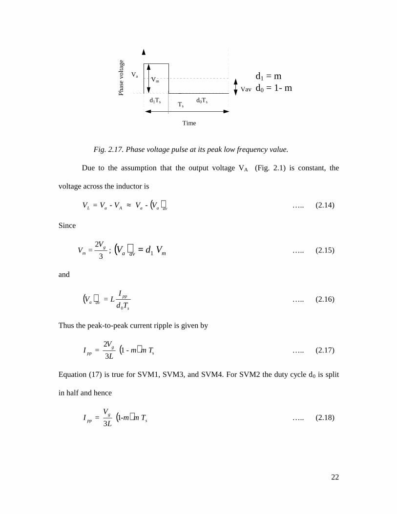
Maximum output current ripple occurs when the volt-second across the output
inductors is the largest. Consider phase ‘a’ in Fig. 2.1 and assume that output voltage VA
(Fig.2.1) varies slowly with respect to the switching frequency. Then for a passive load,
the maximum volt-second across the inductor in phase ‘a’ occurs when the reference
vector in Fig. 2.7 is collinear with the switching vector V1(pnn). At this instant the duty
cycle d2 = 0 and duty cycle d1 = m, and the resultant phase voltage will be as shown in
Fig. 2.17.
Load power factor angle
Rel
ativ
e sw
itchi
ng lo
sses
22
Tsd1Ts
Vm
d0Ts
Vav
Va d1 = md0 = 1- m
Fig. 2.17. Phase voltage pulse at its peak low frequency value.
Due to the assumption that the output voltage VA (Fig. 2.1) is constant, the
voltage across the inductor is
( )avaaA aL V - V - V = VV ≈ ….. (2.14)
Since
3
2 = g
m
VV ; ( ) mava VdV 1= ….. (2.15)
and
( )s
pp
ava Td
I = LV
0
….. (2.16)
Thus the peak-to-peak current ripple is given by
( ) 13
2s m T - m
L
V = I g
pp ….. (2.17)
Equation (17) is true for SVM1, SVM3, and SVM4. For SVM2 the duty cycle d0 is split
in half and hence
( ) m T-m L
V = I s
gpp 1
3….. (2.18)
TimeP
hase
vo
ltage

23
Fig. 2.18 shows the plot of the relative peak-to-peak ripple current, based on the above
analysis and based on the simulation results using SABER , for the entire range of
modulation index.
Modulation index (m)0 0.866
Fig. 2.18. Relative peak-to-peak current ripple.
2.6 Simulation and Experimental Results
The circuit in Fig. 2.1 was simulated using SABER. Appendix A gives the listing
of the space vector modulation template developed in MAST for SVM1. The circuit in
Fig. 2.1 was simulated using ideal switches, RCD snubbers, and ideal diodes, using the
following parameters: Vg = 16 V, Iload = 6.5 A, fo = 108 Hz, fs = 3888 Hz, m = 0.6. The
output current waveforms and their spectra are shown in Fig. 2.19. Fig. 2.20 shows the
waveforms of the output current and spectrum of output current obtained from an
experimental inverter running under similar conditions. The figures show a fairly good
agreement between simulation and experimental results.
Re
lativ
e p
ea
k-to
-pe
ak
rip
ple

24
SVM1
SVM2
SVM3
SVM4
Fig. 2.19. Simulated line currents and spectrum of line currents ( fs/fo = 36).

25
Fig. 2.20. Experimental line currents and spectrum of line currents (fs/fo = 36).

26
2.7 PERFORMANCE SUMMARY
Table 2.2 summarizes the performance of four space vector modulation schemes.
It can be clearly seen that a scheme with high THD has low losses and vice versa and
these characteristics are load dependent. This could be translated as a trade-off to be made
between the size of the heat sink and size of the filters. At low switching frequencies
SVM2 could be used, since losses are not very critical. At high switching frequencies
SVM4 is preferred, especially at high load power factors due to the 50% reduction in
switching losses. SVM3 could be used at low load power factors.
The right aligned sequence (SVM1) (or the left-aligned sequence) does not seem
to have any particular advantage if the converter is hard switched. However, if soft-
switching is introduced then this scheme is particularly useful because here all the three
legs are being switched at the same time.
It has also been observed that the performance of SVM4 can be improved by
introducing symmetry. This result’s in reduced THD and in reduced peak-to-peak ripple
in the load current; with the switching losses remaining the same.
. Table 2.2. Relative performance of various modulation schemes (three-leg).
Modulation Schemes SVM1 SVM2 SVM3 SVM4No of commutations in Ts 6 6 3 4Relative Losses 1 1 0.5 0.5-0.63**
Dominant harmonic fs fs fs/2 fsTHD at low mod index LeastTHD at high mod. index Least HighestRelative peak-to-peak ripple at Imax 1 0.5 1 1Number of switching states in Ts 4 7 3 3** Depending on the load power factor* Important for digital modulator implementation
Copyright © 2022 FDOKUMEN