Early stabilizing alveolar ventilation prevents acute respiratory distress syndrome
Upload
khangminh22Category
view
4download
0
Nanoscalersc.li/nanoscale
ISSN 2040-3372
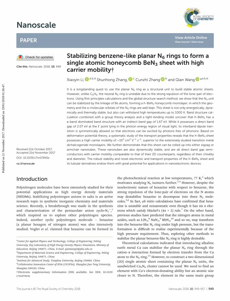
PAPER Qian Wang et al. Stabilizing benzene-like planar N
6 rings to form a single atomic
honeycomb BeN 3 sheet with high carrier mobility
Volume 10 Number 3 21 January 2018 Pages 859–1548
Nanoscale
PAPER
Cite this: Nanoscale, 2018, 10, 949
Received 21st October 2017,Accepted 21st November 2017
DOI: 10.1039/c7nr07845e
rsc.li/nanoscale
Stabilizing benzene-like planar N6 rings to form asingle atomic honeycomb BeN3 sheet with highcarrier mobility†
Xiaoyin Li, a,b,d Shunhong Zhang, c Cunzhi Zhang b and Qian Wang *a,b,d
It is a longstanding quest to use the planar N6 ring as a structural unit to build stable atomic sheets.
However, unlike C6H6, the neutral N6 ring is unstable due to the strong repulsion of the lone-pair of elec-
trons. Using first-principles calculations and the global structure search method, we show that the N6 unit
can be stabilized by the linkage of Be atoms, forming a h-BeN3 honeycomb monolayer, in which the geo-
metry and the π-molecular orbitals of the N6 rings are well kept. This sheet is not only energetically, dyna-
mically and thermally stable, but also can withstand high temperatures up to 1000 K. Band structure cal-
culation combined with a group theory analysis and a tight-binding model uncover that h-BeN3 has a
π-band dominated band structure with an indirect band gap of 1.67 eV. While it possesses a direct band
gap of 2.07 eV at the Γ point lying in the photon energy region of visual light, its interband dipole tran-
sition is symmetrically allowed so that electrons can be excited by photons free of phonons. Based on
deformation potential theory, a systematic study of the transport properties reveals that the h-BeN3 sheet
possesses a high carrier mobility of ∼103 cm2 V−1 s−1, superior to the extensively studied transition metal
dichalcogenide monolayers. We further demonstrate that this sheet can be rolled up into either zigzag or
armchair nanotubes. These nanotubes are also dynamically stable, and are all direct band gap semi-
conductors with carrier mobility comparable to that of their 2D counterparts, regardless of their chirality
and diameter. The robust stability and novel electronic and transport properties of the h-BeN3 sheet and
its tubular derivatives endow them with great potential for applications in nanoelectronic devices.
Introduction
Polynitrogen molecules have been extensively studied for theirpotential applications as high energy density materials(HEDMs). Stabilizing polynitrogen anions in salts is an activeresearch topic in synthetic inorganic chemistry and materialsscience. Recently, a breakthrough was made in the synthesisand characterization of the pentazolate anion cyclo-N5
−,1
which inspired us to explore other polynitrogen species.Indeed, another cyclic polynitrogen molecule – hexazine(a planar hexagon of nitrogen atoms) was also intensivelystudied. Vogler et al. claimed that hexazine can be formed in
the photochemical reaction at low temperatures, 77 K,2 whichmotivates studying N6 isomers further.3,4 However, despite theisoelectronic nature of hexazine with respect to benzene, thestrong repulsion of the lone-pair of electrons on the N atomsmay destabilize hexazine to decompose into three N2 mole-cules.5,6 In fact, ab initio calculations have confirmed that hexa-zine is unstable and nonaromatic even though it has six π elec-trons which satisfy Hückel’s (4n + 2) rule.7 On the other hand,previous studies have predicted that the nitrogen atoms in metalazides, such as LiN3,
8 NaN3,9 RbN3,
10 and so on, may transforminto the benzene-like N6 ring under high pressure, but the trans-formation is difficult to realize experimentally because of thehigh pressure requirement. Thus, exploring other methods tostabilize the planar benzene-like N6 ring is highly desirable.
Theoretical calculations indicated that introducing alkalineearth metal Ca can stabilize the planar N6 ring through thecation–π interaction formed by electron transfer from the Caatom to the N6 ring.
11 However, to construct a two dimensional(2D) single atomic sheet containing the planar N6 units, thesandwiched Ca2N6 cluster cannot be used. We need to find anelement with Ca’s electron-donating ability but an atomic sizecloser to N. Therefore, the element in the same main group
†Electronic supplementary information (ESI) available. See DOI: 10.1039/c7nr07845e
aCenter for Applied Physics and Technology, College of Engineering, Peking
University; Key Laboratory of High Energy Density Physics Simulation, Ministry of
Education, Beijing 100871, China. E-mail: [email protected] of Materials Science and Engineering, College of Engineering, Peking
University, Beijing 100871, ChinacInstitute for Advanced Study, Tsinghua University, Beijing 100084, ChinadCollaborative Innovation Center of IFSA (CICIFSA), Shanghai Jiao Tong University,
Shanghai 200240, China
This journal is © The Royal Society of Chemistry 2018 Nanoscale, 2018, 10, 949–957 | 949
Publ
ishe
d on
21
Nov
embe
r 20
17. D
ownl
oade
d on
19/
01/2
018
01:3
6:47
.
View Article OnlineView Journal | View Issue
with Ca but having a smaller atomic size can be expected towork for this purpose. In this paper, by means of a particle-swarm optimization (PSO) based global structure searchmethod, we have verified that Be atoms can be used to link theplanar N6 rings forming a honeycomb BeN3 (h-BeN3) singleatomic sheet, which is the lowest-energy planar structure. Byanalyzing the structural stability from multiple criteria regard-ing thermodynamics, lattice dynamics, and thermal pertur-bations, we confirmed that the benzene-like N6 rings can bestabilized in the 2D h-BeN3 sheet under ambient conditions.We systematically studied the vibrational, mechanical, elec-tronic and transport properties of h-BeN3 via first principlescalculations combined with the tight-binding method. Thecorresponding nanotube derivatives of the h-BeN3 sheet arealso explored.
Computational methods
The ground state structure search is performed using a par-ticle-swarm optimization (PSO) based global structure searchmethod implemented in the Crystal structure AnaLYsis by theParticle Swarm Optimization (CALYPSO) code,12,13 which hasbeen successfully employed to predict many 2D structures atgiven chemical compositions.14–16 In our simulations, unitcells containing a total of 8, 16, and 20 atoms are considered.For each simulation, the structure search lasts for 20 gene-ration loops, and in each loop 20 different structures are opti-mized. DFT calculations are mainly performed using theVienna Ab initio Simulation Package (VASP).17 The Projector
Augmented Wave (PAW) method18 is adopted with a kineticenergy cut off of 520 eV. The Perdew–Burke–Ernzerhof (PBE)functional19 with the Generalized Gradient Approximation20 isused to treat the electron exchange–correlation interactionsin most calculations, while Heyd–Scuseria–Ernzerhof(HSE06)21,22 which includes the Hartree–Fock exchange energyand the Coulomb screening effect is also used for more accu-rate electronic band gaps. The Brillouin zone is represented bythe k point mesh following the Monkhorst–Pack scheme,23
with a grid density of 2π × 0.02 Å−1. Lattice constants andatomic positions are relaxed using the conjugated gradientalgorithm without any symmetry-related constraint. The con-vergence threshold of total energy and atomic force com-ponents are 10−5 eV and 10−3 eV Å−1, respectively. Phonon dis-persion and density of states (DOS) are calculated using thefinite displacement method24 as implemented in the Phonopycode.25 A (6 × 6) supercell is constructed to calculate theatomic force under finite displacements and derive thedynamics matrix. The tight-binding (TB) Hamiltonian is con-structed based on the maximally localized Wannier functions(MLWFs) with the hopping parameters calculated using theWannier90 package26 interfaced with the Quantum ESPRESSOcode.27
Results and discussionStructure and stability
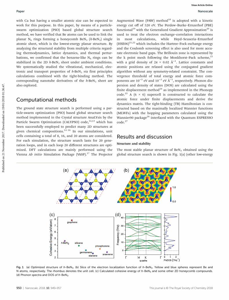
The most stable planar structure of BeN3 obtained using theglobal structure search is shown in Fig. 1(a) (other low-energy
Fig. 1 (a) Optimized structure of h-BeN3. (b) Slice of the electron localization function of h-BeN3. Yellow and blue spheres represent Be andN atoms, respectively. The rhombus denotes the unit cell. (c) Calculated cohesive energy of h-BeN3 and some other 2D honeycomb compounds.(d) Phonon spectra and DOS of h-BeN3.
Paper Nanoscale
950 | Nanoscale, 2018, 10, 949–957 This journal is © The Royal Society of Chemistry 2018
Publ
ishe
d on
21
Nov
embe
r 20
17. D
ownl
oade
d on
19/
01/2
018
01:3
6:47
. View Article Online
isomers are shown in Fig. S1†). We term it as h-BeN3 becauseof its honeycomb lattice. Similar to graphene, h-BeN3 is a flatmonolayer with the highest plane symmetry of P6mm (planegroup no. 17). Be and N atoms are located at the 2b (1/3, 2/3)and 6e (x, −x) 2D Wyckoff positions, respectively, with x =0.152828. The optimized lattice constants are a = b = 5.14 Å.The N–N and Be–N bond lengths are 1.36 and 1.61 Å, respect-ively. Interestingly, we note that h-BeN3 is isostructural to theexperimentally synthesized monolayer h-BC3
28 and h-C3N,29 as
well as the theoretically predicted h-SiC3.30,31 However,
different from those 2D compounds, h-BeN3 contains planarN6 hexagons rather than C6 hexagons. It has been demon-strated that the charge transfer from Ca to the N6 ring in theCa2N6 cluster contributes to the structure stability.11 Thus, westudy the charge transfer and bonding nature of h-BeN3 by cal-culating its electron localization function (ELF). From the ELFslice, as shown in Fig. 1(b), we see that the N6 ring is electronabundant while the Be atoms are electron deficient. To getmore insight, we perform the Bader charge analysis.32 Theresults suggest that each Be atom transfers ∼1.67 electrons tothe N atoms. Consequently, each N6 ring receives ∼3.34 elec-trons (quite close to that of ∼3.3 electrons in the Ca2N6
cluster11), which distribute uniformly on the N sites. This indi-cates that the N6 ring is nearly quadruply charged like the N6
moiety in the Ca2N6 cluster, which is crucial to the structuralstability.
We then carefully examine the structural stability of h-BeN3
from the perspectives of both energetics and dynamics. Firstof all, we calculate the cohesive energy of h-BeN3, which isdefined as Ec = [E(Be) + 3E(N) − E(h-BeN3)]/4. The calculatedcohesive energy is 4.72 eV per atom. For comparison, we calcu-late the cohesive energy of some other experimentally syn-thesized or theoretically predicted 2D honeycomb compoundsusing the same method and criteria of accuracy. The resultsare listed in Fig. 1(c). Our calculated cohesive energies of gra-phene, silicene, germanene, stanene, phosphorene, andarsenene are 7.97, 3.97, 3.26, 2.76, 3.48 and 2.96 eV per atom,respectively, in excellent agreement with previous studies.33–35
The cohesive energy of h-BeN3 is larger than that of experi-mentally synthesized 2D materials, such as silicene and phos-phorene, implying the possibility of realizing such a 2D sheet.
We also calculate the formation energy of h-BeN3 by usingthe following formula:
Efðh-BeN3Þ ¼ ð1=4ÞμðBeÞ þ ð3=4ÞμðNÞ � Ecðh-BeN3Þ; ð1Þ
where Ec (h-BeN3) is the cohesive energy of h-BeN3, and μ(Be)and μ(N) are the chemical potentials of Be and N, which aretaken from the cohesive energies of hexagonal-close-packed(hcp) Be and N2, respectively. The calculated formation energyof h-BeN3 is 107 meV per atom. Although its formation energyis higher than that of the three-dimensional (3D) Be3N2 struc-ture, it is smaller than that of the experimentally synthesized2D g-C3N4
36–38 (349 meV per atom, using graphene and N2 asreferences). Moreover, it has been verified by many known 2Dmaterials that 2D atomic sheets with a formation energy lower
than 200 meV per atom are likely to exist in the freestandingform.39 Besides, when using hcp Be and N6 molecules as refer-ences, the formation energy of h-BeN3 becomes −787 meV peratom. The negative value indicates that the reaction is exother-mic. In this sense, it is possible to synthesize h-BeN3
experimentally.Since lattice dynamics also plays an important role in the
stability of crystals, we calculate the phonon spectra of h-BeN3.The results, plotted in Fig. 1(d), show that there are no imagin-ary modes in the entire Brillouin zone, confirming that h-BeN3
is dynamically stable. For future experimental characterization,we calculate the infrared (IR) and Raman spectra corres-ponding to the vibration modes at the first Brillouin zonecenter. The calculated results in Fig. S2 (ESI†) indicate thatthere are two (four) peaks in the IR (Raman) spectra corres-ponding to four (seven) vibration modes with E1u (A1g or E2g)symmetry.
We also perform ab initio molecular dynamics (AIMD) simu-lations to examine the thermal stability of h-BeN3. A (5 × 5)hexagonal supercell (containing 200 atoms) and a (3√3 × 4)rectangle supercell (containing 192 atoms) are constructed,respectively, to perform individual AIMD simulations. Afterbeing heated at 300 K for 10 ps, the structure retains its integ-rity without any visible distortions, and the total potentialenergy fluctuates closely around the norm (see Fig. S3†),suggesting that h-BeN3 is thermally stable at room temperaturewith the planar N6 rings unaffected. Furthermore, our calcu-lations show that the h-BeN3 sheet can withstand temperaturesas high as 1000 K (see Fig. S4†), implying the high thermalstability of the 2D structure.
Because the lattice is fixed during the AIMD simulations,we also calculate the elastic constants to study the mechanicalstability of h-BeN3 under small lattice distortion. Through thefinite distortion approach,40 we obtain C11 = C22 = 199 N m−1,C12 = 52 N m−1, and C66 = 74 N m−1, which satisfy the Born cri-teria, C11 > |C12| > 0 and C66 > 0. Due to the hexagonal sym-metry, the in-plane mechanical properties of h-BeN3 are iso-tropic. From the elastic constants, we derive the Young’smodulus and the Poisson’s ratio to be 186 N m−1 and 0.26,respectively. The Young’s modulus is half of that of graphene(345 N m−1)41 but is larger than that of other known honey-comb sheets like H-MoS2 (120 N m−1).42 The high in-planestiffness of h-BeN3 implies the strong bonding in the com-pound which is beneficial for its stability.
Electronic properties
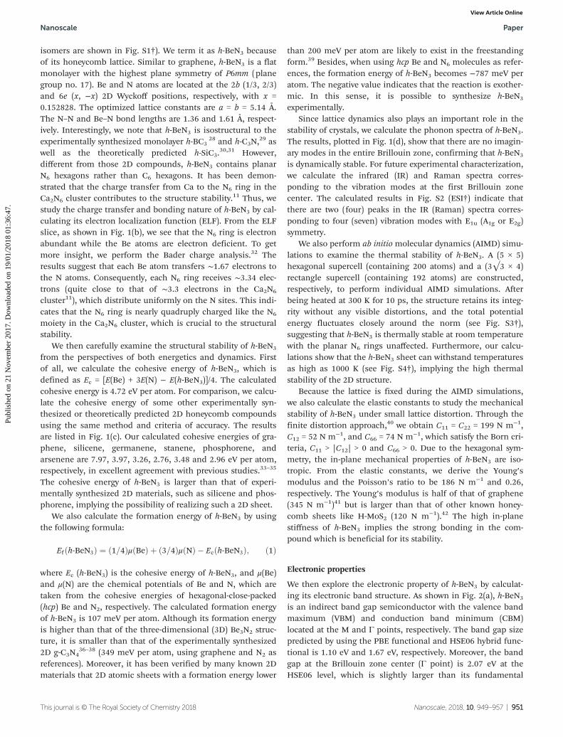
We then explore the electronic property of h-BeN3 by calculat-ing its electronic band structure. As shown in Fig. 2(a), h-BeN3
is an indirect band gap semiconductor with the valence bandmaximum (VBM) and conduction band minimum (CBM)located at the M and Γ points, respectively. The band gap sizepredicted by using the PBE functional and HSE06 hybrid func-tional is 1.10 eV and 1.67 eV, respectively. Moreover, the bandgap at the Brillouin zone center (Γ point) is 2.07 eV at theHSE06 level, which is slightly larger than its fundamental
Nanoscale Paper
This journal is © The Royal Society of Chemistry 2018 Nanoscale, 2018, 10, 949–957 | 951
Publ
ishe
d on
21
Nov
embe
r 20
17. D
ownl
oade
d on
19/
01/2
018
01:3
6:47
. View Article Online
band gap (1.67 eV) but close to that of H-MoS2 (2.13 eV)43 andwithin the photon energy range of visual light.
To identify the possibility of direct optical excitation at theΓ point, we examine its dipole transition allowance. The wave-function symmetry of the highest occupied state and thelowest unoccupied state at the Γ point are E2u and B1g, respect-ively. The point group of the Γ point is D6h, according to grouptheory, and the dipole moment operator is A2u⊕E1u.Accordingly, the dipole transition can be described by the fol-lowing formula:
E2u � ðA2u � E1uÞ � B1g ¼ A1g � A2g � E1g � E2g: ð2Þ
We see that A1g is included in the right-hand term, indicat-ing that dipole transition is symmetry allowed at the Γ point sothat electrons can be excited by photons without the assistanceof phonons.
To determine the orbital composition of the energy bands,we calculate the orbital decomposed band structure of h-BeN3
which is shown in Fig. 2(b). This demonstrates that the high-lying occupied bands are mainly derived from the p orbitalswhile the occupied bands originating from the s orbitals aredeep-lying. More importantly, it shows that near the Fermilevel there are six bands which are only from pz orbitals.Therefore, it is possible and reasonable to model these elec-tronic states using a simple TB Hamiltonian of N-pz orbitals:
H ¼ UXi
ciþci þXi=j
ðtijciþcj þ h:c:Þ: ð3Þ
Here, ci+ and ci represent the creation and annihilation
operators of an electron in the ith N-pz orbital, U is the onsiteenergy and tij is the hopping integral parameter between theith and jth N-pz orbitals. For simplicity, we only consider thenearest-neighbor intra-ring and inter-ring (the hexagonal N6
ring) hoppings between the N-pz orbitals, as illustrated inFig. S5.† By fitting the DFT band structure using the MLWFsas the basis, the onsite energy U, and the intra- and inter-ringhopping integral parameters t1 and t2 are determined to be−3.09, −2.60 and −0.41 eV, respectively. By diagonalizing the
TB model Hamiltonian, we obtain the electronic bands ofh-BeN3 (shown in Fig. 2(c)), which reproduce well the bandalignment and dispersion features from the DFT band struc-ture. In this sense, we have designed a π-band dominated 2Dsemiconductor with an intermediate band gap size betweengapless graphene and wide-gap h-BN monolayer.
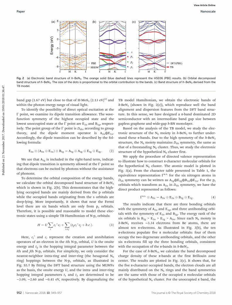
Based on the analysis of the TB model, we study the elec-tronic structure of the N6 moiety in h-BeN3 to further under-stand these π-bands. Due to the high symmetry of the h-BeN3
structure, the N6 moiety maintains D6h symmetry, the same asthat of a freestanding N6 cluster. Thus, we study the electronicstructure of the hypothetical N6 cluster first.
We apply the procedure of directed valence representationto illustrate how to construct π-character molecular orbitals forthe hypothetical N6 cluster. The atomic model is plotted inFig. 3(a). From the character table presented in Table 1, theequivalence representation Γa.s. for the six nitrogen atoms inD6h symmetry can be written as A1g⊕E2g⊕B1u⊕E1u. For the pzorbitals which transform as A2u in D6h symmetry, we have thedirect product represented as follows:
Γa:s: � A2u ¼ A2u � E2u � B2g � E1g: ð4ÞThe results indicate that there are three bonding orbitals
with the symmetry of A2u and E1g, and three antibonding orbi-tals with the symmetry of E2u and B2g. The energy rank of thesix orbitals is B2g > E2u > E1g > A2u. Since each N6 moiety inh-BeN3 receives ∼3.34 electrons from Be atoms, there arealmost ten π-electrons. As illustrated in Fig. 3(b), the tenπ-electrons populate five π molecular orbitals: four of themoccupy the two degenerate antibonding orbitals, and the othersix π-electrons fill up the three bonding orbitals, consistentwith the occupation of the π-bands in h-BeN3.
For the case of h-BeN3, we calculate the band decomposedcharge density of these π-bands at the first Brillouin zonecenter. The results are plotted in Fig. 3(c). It shows that, forthe five π-character occupied bands, the electron clouds are allmainly distributed on the N6 rings and the band symmetriesare the same with those of the occupied π molecular orbitalsof the hypothetical N6 cluster. For the unoccupied π band, the
Fig. 2 (a) Electronic band structure of h-BeN3. The orange solid (blue dashed) lines represent the HSE06 (PBE) results. (b) Orbital decomposedband structure of h-BeN3. The size of the dots is proportional to the orbital contribution to the bands. (c) Band structure of h-BeN3 derived from theTB model.
Paper Nanoscale
952 | Nanoscale, 2018, 10, 949–957 This journal is © The Royal Society of Chemistry 2018
Publ
ishe
d on
21
Nov
embe
r 20
17. D
ownl
oade
d on
19/
01/2
018
01:3
6:47
. View Article Online
electron clouds locate both on the N atoms and Be atoms,resulting in the band symmetry differing from that of theunoccupied π molecular orbital of the hypothetical N6 cluster.It demonstrates the well-maintained integrity of π molecularorbitals of N6 in h-BeN3, even in the presence of adjacent Beatoms.
Transport properties
Because of the moderate band gap size and the dipole allowedtransition at the Brillouin zone center, we further explore thetransport properties of h-BeN3 for its potential electronic appli-cations. To this end, we calculate the carrier mobility inh-BeN3 using the deformation potential (DP) theory proposedby Bardeen and Shockley.44 The analytical expression forcarrier mobility (μ) of 2D semiconducting materials can bewritten as:
μ ¼ 2eħ3C3kBT jm*j2E12
; ð5Þ
which has been successfully employed to study the chargetransport in many 2D semiconductors, such as phosphorene,45
monolayer MoS2,46 TiS3,
47 and GeP3.48 Here C is the elastic
modulus of the 2D sheet, T is the temperature, which is takento be 300 K in our calculations, and m* = ħ2[∂2E(k)/∂k2]−1 is theeffective mass of the band edge carrier along the transportdirection. E1 is the DP constant defined as the energy shift ofthe band edge with respect to lattice dilation and compression,and kB and ħ are Boltzmann and reduced Planck constants,respectively. Here we use an orthogonal supercell to studycarrier mobilities along the zigzag and armchair directions.The atomic structure of the supercell and corresponding elec-tronic band structure are presented in Fig. S6.† All the calcu-lated results (m*, E1, C, μ) are summarized in Table 2. One cansee that the electron has higher mobility than the hole in bothtransport directions. Thus h-BeN3 can be considered an n-typesemiconductor. The smaller hole mobility is primarily attribu-ted to its larger effective mass, which can be deduced from theelectronic band structure (see Fig. S6†). Remarkably, thecarrier mobility in h-BeN3 can be as high as 9.89 × 103 cm2 V−1 s−1
for an electron transporting along the armchair direction,which is comparable to that of phosphorene,45 TiS3
47 andGeP3,
48 and much higher than that of monolayer MoS2,46 and
other monolayer transition metal dichalcogenide materials,49
indicating potential applications of h-BeN3 in nanoelectronics.
Nanotube derivatives
As an extension of the current study, we investigate an impor-tant derivative of the honeycomb h-BeN3 sheet, namely, theh-BeN3 nanotube. We study the two main types of nanotubes,the zigzag (n, 0) and armchair (n, n) nanotubes, as illustratedin Fig. 4(a). A series of zigzag (n, 0) (4 < n < 13), and armchair(n, n) (2 < n < 8) nanotubes are systematically studied toexplore their electronic properties.
First of all, we calculate the strain energies of the nano-tubes, which are obtained by subtracting the total energy ofthe h-BeN3 sheet from that of the optimized h-BeN3 nanotubes.
Fig. 3 (a) Atomic model of the hypothetical N6 cluster. The two-foldrotation axes of point group D6h are illustrated. (b) Diagram of π mole-cular orbitals derived from the pz orbitals of N atoms. (c) The firstBrillouin zone center band decomposed charge density of h-BeN3,corresponding to the six π bands. The isovalue is 0.03 e Å−3.
Table 1 Characters for the Γa.s. representation of six nitrogen atoms in the hypothetic N6 cluster, and transformation representation of pz orbitals(D6h symmetry)
E 2C6 2C3 C2 3C′2 3C″2 I 2S3 2S6 σh 3σd 3σv
Γa.s (N6) (A1g⊕E2g⊕B1u⊕E1u) 6 0 0 0 2 0 0 0 0 6 0 2Γ(pz) (A2u) 1 1 1 1 −1 −1 −1 −1 −1 −1 1 1
Table 2 Deformation potential constant E1, elastic modulus C, effectivemass m* and mobility μ for electron and hole along the zigzag and arm-chair directions in the h-BeN3 sheet at 300 K
Carrier type E1 (eV)C(N m−1)
m*(me)
μ (×103 cm2
V−1 s−1)
Electron Zigzag −2.25 199 0.24 9.72Armchair −2.23 199 0.24 9.89
Hole Zigzag −2.93 199 0.51 1.27Armchair −3.95 199 1.78 0.06
Nanoscale Paper
This journal is © The Royal Society of Chemistry 2018 Nanoscale, 2018, 10, 949–957 | 953
Publ
ishe
d on
21
Nov
embe
r 20
17. D
ownl
oade
d on
19/
01/2
018
01:3
6:47
. View Article Online
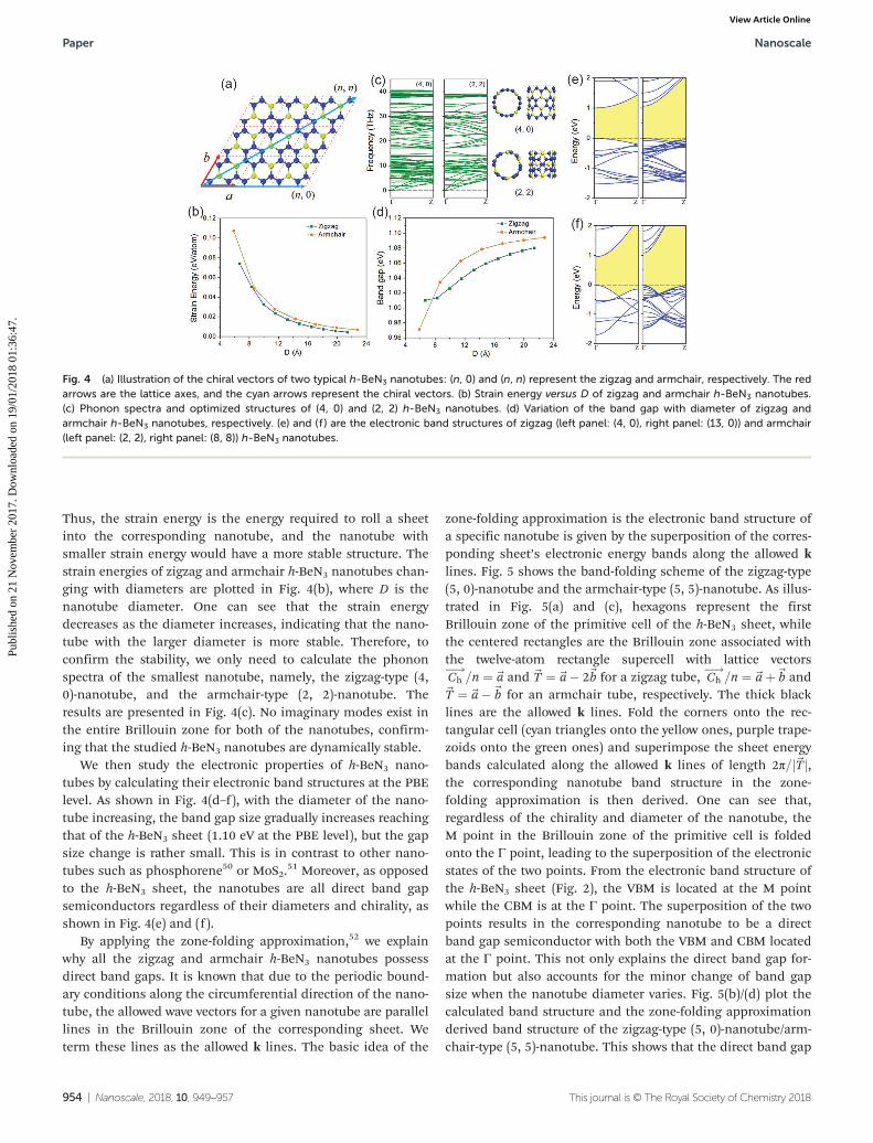
Thus, the strain energy is the energy required to roll a sheetinto the corresponding nanotube, and the nanotube withsmaller strain energy would have a more stable structure. Thestrain energies of zigzag and armchair h-BeN3 nanotubes chan-ging with diameters are plotted in Fig. 4(b), where D is thenanotube diameter. One can see that the strain energydecreases as the diameter increases, indicating that the nano-tube with the larger diameter is more stable. Therefore, toconfirm the stability, we only need to calculate the phononspectra of the smallest nanotube, namely, the zigzag-type (4,0)-nanotube, and the armchair-type (2, 2)-nanotube. Theresults are presented in Fig. 4(c). No imaginary modes exist inthe entire Brillouin zone for both of the nanotubes, confirm-ing that the studied h-BeN3 nanotubes are dynamically stable.
We then study the electronic properties of h-BeN3 nano-tubes by calculating their electronic band structures at the PBElevel. As shown in Fig. 4(d–f ), with the diameter of the nano-tube increasing, the band gap size gradually increases reachingthat of the h-BeN3 sheet (1.10 eV at the PBE level), but the gapsize change is rather small. This is in contrast to other nano-tubes such as phosphorene50 or MoS2.
51 Moreover, as opposedto the h-BeN3 sheet, the nanotubes are all direct band gapsemiconductors regardless of their diameters and chirality, asshown in Fig. 4(e) and (f ).
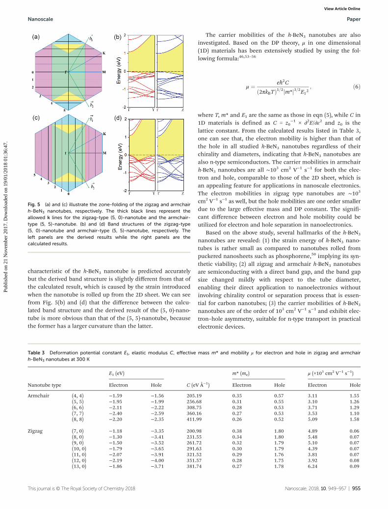
By applying the zone-folding approximation,52 we explainwhy all the zigzag and armchair h-BeN3 nanotubes possessdirect band gaps. It is known that due to the periodic bound-ary conditions along the circumferential direction of the nano-tube, the allowed wave vectors for a given nanotube are parallellines in the Brillouin zone of the corresponding sheet. Weterm these lines as the allowed k lines. The basic idea of the
zone-folding approximation is the electronic band structure ofa specific nanotube is given by the superposition of the corres-ponding sheet’s electronic energy bands along the allowed klines. Fig. 5 shows the band-folding scheme of the zigzag-type(5, 0)-nanotube and the armchair-type (5, 5)-nanotube. As illus-trated in Fig. 5(a) and (c), hexagons represent the firstBrillouin zone of the primitive cell of the h-BeN3 sheet, whilethe centered rectangles are the Brillouin zone associated withthe twelve-atom rectangle supercell with lattice vectorsCh�!
=n ¼~a and ~T ¼~a� 2~b for a zigzag tube, Ch�!
=n ¼~aþ~b and~T ¼~a�~b for an armchair tube, respectively. The thick blacklines are the allowed k lines. Fold the corners onto the rec-tangular cell (cyan triangles onto the yellow ones, purple trape-zoids onto the green ones) and superimpose the sheet energybands calculated along the allowed k lines of length 2π=j~T j,the corresponding nanotube band structure in the zone-folding approximation is then derived. One can see that,regardless of the chirality and diameter of the nanotube, theM point in the Brillouin zone of the primitive cell is foldedonto the Γ point, leading to the superposition of the electronicstates of the two points. From the electronic band structure ofthe h-BeN3 sheet (Fig. 2), the VBM is located at the M pointwhile the CBM is at the Γ point. The superposition of the twopoints results in the corresponding nanotube to be a directband gap semiconductor with both the VBM and CBM locatedat the Γ point. This not only explains the direct band gap for-mation but also accounts for the minor change of band gapsize when the nanotube diameter varies. Fig. 5(b)/(d) plot thecalculated band structure and the zone-folding approximationderived band structure of the zigzag-type (5, 0)-nanotube/arm-chair-type (5, 5)-nanotube. This shows that the direct band gap
Fig. 4 (a) Illustration of the chiral vectors of two typical h-BeN3 nanotubes: (n, 0) and (n, n) represent the zigzag and armchair, respectively. The redarrows are the lattice axes, and the cyan arrows represent the chiral vectors. (b) Strain energy versus D of zigzag and armchair h-BeN3 nanotubes.(c) Phonon spectra and optimized structures of (4, 0) and (2, 2) h-BeN3 nanotubes. (d) Variation of the band gap with diameter of zigzag andarmchair h-BeN3 nanotubes, respectively. (e) and (f ) are the electronic band structures of zigzag (left panel: (4, 0), right panel: (13, 0)) and armchair(left panel: (2, 2), right panel: (8, 8)) h-BeN3 nanotubes.
Paper Nanoscale
954 | Nanoscale, 2018, 10, 949–957 This journal is © The Royal Society of Chemistry 2018
Publ
ishe
d on
21
Nov
embe
r 20
17. D
ownl
oade
d on
19/
01/2
018
01:3
6:47
. View Article Online
characteristic of the h-BeN3 nanotube is predicted accuratelybut the derived band structure is slightly different from that ofthe calculated result, which is caused by the strain introducedwhen the nanotube is rolled up from the 2D sheet. We can seefrom Fig. 5(b) and (d) that the difference between the calcu-lated band structure and the derived result of the (5, 0)-nano-tube is more obvious than that of the (5, 5)-nanotube, becausethe former has a larger curvature than the latter.
The carrier mobilities of the h-BeN3 nanotubes are alsoinvestigated. Based on the DP theory, μ in one dimensional(1D) materials has been extensively studied by using the fol-lowing formula:46,53–56
μ ¼ eħ2C
ð2πkBTÞ1=2jm*j3=2E12; ð6Þ
where T, m* and E1 are the same as those in eqn (5), while C in1D materials is defined as C = z0
−1 × ∂2E/∂ε2 and z0 is thelattice constant. From the calculated results listed in Table 3,one can see that, the electron mobility is higher than that ofthe hole in all studied h-BeN3 nanotubes regardless of theirchirality and diameters, indicating that h-BeN3 nanotubes arealso n-type semiconductors. The carrier mobilities in armchairh-BeN3 nanotubes are all ∼103 cm2 V−1 s−1 for both the elec-tron and hole, comparable to those of the 2D sheet, which isan appealing feature for applications in nanoscale electronics.The electron mobilities in zigzag type nanotubes are ∼103
cm2 V−1 s−1 as well, but the hole mobilities are one order smallerdue to the large effective mass and DP constant. The signifi-cant difference between electron and hole mobility could beutilized for electron and hole separation in nanoelectronics.
Based on the above study, several hallmarks of the h-BeN3
nanotubes are revealed: (1) the strain energy of h-BeN3 nano-tubes is rather small as compared to nanotubes rolled frompuckered nanosheets such as phosphorene,50 implying its syn-thetic viability; (2) all zigzag and armchair h-BeN3 nanotubesare semiconducting with a direct band gap, and the band gapsize changed mildly with respect to the tube diameter,enabling their direct application to nanoelectronics withoutinvolving chirality control or separation process that is essen-tial for carbon nanotubes; (3) the carrier mobilities of h-BeN3
nanotubes are of the order of 103 cm2 V−1 s−1 and exhibit elec-tron–hole asymmetry, suitable for n-type transport in practicalelectronic devices.
Fig. 5 (a) and (c) illustrate the zone-folding of the zigzag and armchairh-BeN3 nanotubes, respectively. The thick black lines represent theallowed k lines for the zigzag-type (5, 0)-nanotube and the armchair-type (5, 5)-nanotube. (b) and (d) Band structures of the zigzag-type(5, 0)-nanotube and armchair-type (5, 5)-nanotube, respectively. Theleft panels are the derived results while the right panels are thecalculated results.
Table 3 Deformation potential constant E1, elastic modulus C, effective mass m* and mobility μ for electron and hole in zigzag and armchairh-BeN3 nanotubes at 300 K
Nanotube type
E1 (eV)
C (eV Å−1)
m* (me) μ (×103 cm2 V−1 s−1)
Electron Hole Electron Hole Electron Hole
Armchair (4, 4) −1.59 −1.56 205.19 0.35 0.57 3.11 1.55(5, 5) −1.95 −1.99 256.68 0.31 0.55 3.10 1.26(6, 6) −2.11 −2.22 308.75 0.28 0.53 3.71 1.29(7, 7) −2.40 −2.59 360.16 0.27 0.53 3.53 1.10(8, 8) −2.20 −2.35 411.99 0.26 0.52 5.09 1.58
Zigzag (7, 0) −1.18 −3.35 200.98 0.38 1.80 4.89 0.06(8, 0) −1.30 −3.41 231.55 0.34 1.80 5.48 0.07(9, 0) −1.50 −3.52 261.72 0.32 1.79 5.10 0.07(10, 0) −1.79 −3.65 291.63 0.30 1.79 4.39 0.07(11, 0) −2.07 −3.91 321.52 0.29 1.76 3.81 0.07(12, 0) −2.19 −4.00 351.57 0.28 1.75 3.92 0.08(13, 0) −1.86 −3.71 381.74 0.27 1.78 6.24 0.09
Nanoscale Paper
This journal is © The Royal Society of Chemistry 2018 Nanoscale, 2018, 10, 949–957 | 955
Publ
ishe
d on
21
Nov
embe
r 20
17. D
ownl
oade
d on
19/
01/2
018
01:3
6:47
. View Article Online
Conclusions
In summary, we demonstrate, using the PSO based globalstructure search method combined with DFT and the tight-binding method, that Be atoms can be used to stabilize theplanar N6 ring resulting in a nitrogen-rich honeycomb sheet,the h-BeN3 monolayer, which is energetically, dynamically, andthermally stable. In this structure, the benzene-like N6 ringcan stably exist under ambient conditions. The in-planemechanical properties of h-BeN3 are isotropic with Young’smodulus and Poisson’s ratio of 186 N m−1 and 0.26, respect-ively. h-BeN3 is an indirect band gap semiconductor with aband gap of 1.67 eV and a direct band gap of 2.07 eV at theΓ point, and its interband dipole transition at the Γ point issymmetrically allowed according to our group theory analysis.The Γ point band gap size and the dipole transition allowanceimply the possible applications of h-BeN3 in nanoelectronics.In addition, the investigation of zigzag and armchair h-BeN3
nanotubes shows that the tubular derivatives are all directband gap semiconductors. The mechanism of the indirect todirect band gap transition when going from a sheet to a nano-tube is explained by applying the zone-folding approximation.More importantly, the h-BeN3 sheet and the nanotubes allpossess high carrier mobilities of ∼103 cm2 V−1 s−1, notablyhigher than those of the MoS2 monolayer and nanotubes.Electrons are found to move much faster than holes in boththe sheet and nanotubes, showing the typical feature of n-typesemiconductors. This work provides a strategy for the stabiliz-ation of the planar single atomic sheet composed of benzene-like N6 rings. The robust structural stability and novel elec-tronic and transport properties of the h-BeN3 sheet and itstubular derivatives would stimulate experimental efforts for itssynthesis.
Conflicts of interest
There are no conflicts to declare.
Acknowledgements
This work is partially supported by grants from the NationalNatural Science Foundation of China (NSFC-51471004), andthe National Key Research and Development Program of China(2016YFE0127300 and 2017YFA0205003), and supported by theHigh Performance Computing Platform of Peking University,China.
References
1 C. Zhang, C. Sun, B. Hu, C. Yu and M. Lu, Science, 2017,355, 374.
2 A. Vogler, R. E. Wright and H. Kunkely, Angew. Chem., Int.Ed. Engl., 1980, 19, 717.
3 M. N. Glukhovtsev and P. von Ragué Schleyer, Chem. Phys.Lett., 1992, 198, 547.
4 T. M. Klapötke, J. Mol. Struct.: THEOCHEM, 2000, 499, 99.5 T.-K. Ha, R. Cimiraglia and M. T. Nguyen, Chem. Phys. Lett.,
1981, 83, 317.6 H. Huber, Angew. Chem., Int. Ed. Engl., 1982, 21, 64.7 R. Engelke, J. Phys. Chem., 1992, 96, 10789.8 X. Wang, J. Li, J. Botana, M. Zhang, H. Zhu, L. Chen,
H. Liu, T. Cui and M. Miao, J. Chem. Phys., 2013, 139,164710.
9 M. Zhang, K. Yin, X. Zhang, H. Wang, Q. Li and Z. Wu,Solid State Commun., 2013, 161, 13.
10 X. Wang, J. Li, N. Xu, H. Zhu, Z. Hu and L. Chen, Sci. Rep.,2015, 5, 16677.
11 H. Duan, Z. Gong, J. Cheng, W. Zhu, K. Chen and H. Jiang,J. Phys. Chem. A, 2006, 110, 12236.
12 Y. Wang, J. Lv, L. Zhu and Y. Ma, Phys. Rev. B: Condens.Matter Mater. Phys., 2010, 82, 094116.
13 Y. Wang, M. Miao, J. Lv, L. Zhu, K. Yin, H. Liu and Y. Ma,J. Chem. Phys., 2012, 137, 224108.
14 Y. Li, Y. Liao and Z. Chen, Angew. Chem., Int. Ed., 2014, 53,7248.
15 Y. Wang, F. Li, Y. Li and Z. Chen, Nat. Commun., 2016, 7,11488.
16 C. Pu, D. Zhou, Y. Li, H. Liu, Z. Chen, Y. Wang and Y. Ma,J. Phys. Chem. C, 2017, 121, 2669.
17 G. Kresse and J. Furthmüller, Phys. Rev. B: Condens. MatterMater. Phys., 1996, 54, 11169.
18 P. E. Blöchl, Phys. Rev. B: Condens. Matter Mater. Phys.,1994, 50, 17953.
19 J. P. Perdew, K. Burke and M. Ernzerhof, Phys. Rev. Lett.,1996, 77, 3865.
20 Z. Li, P. Wu, C. Wang, X. Fan, W. Zhang, X. Zhai, C. Zeng,Z. Li, J. Yang and J. Hou, ACS Nano, 2011, 5, 3385.
21 J. Heyd, G. E. Scuseria and M. Ernzerhof, J. Chem. Phys.,2003, 118, 8207.
22 J. Heyd, G. E. Scuseria and M. Ernzerhof, J. Chem. Phys.,2006, 124, 219906.
23 H. J. Monkhorst and J. D. Pack, Phys. Rev. B: Solid State,1976, 13, 5188.
24 K. Parlinski, Z. Q. Li and Y. Kawazoe, Phys. Rev. Lett., 1997,78, 4063.
25 A. Togo and I. Tanaka, Scr. Mater., 2015, 108, 1.26 A. A. Mostofi, J. R. Yates, Y.-S. Lee, I. Souza, D. Vanderbilt
and N. Marzari, Comput. Phys. Commun., 2008, 178, 685.27 G. Paolo, B. Stefano, B. Nicola, C. Matteo, C. Roberto,
C. Carlo, C. Davide, L. C. Guido, C. Matteo, D. Ismaila,C. Andrea Dal, G. Stefano de, F. Stefano, F. Guido,G. Ralph, G. Uwe, G. Christos, K. Anton, L. Michele,M.-S. Layla, M. Nicola, M. Francesco, M. Riccardo,P. Stefano, P. Alfredo, P. Lorenzo, S. Carlo, S. Sandro,S. Gabriele, P. S. Ari, S. Alexander, U. Paolo andM. W. Renata, J. Phys.: Condens. Matter, 2009, 21,395502.
28 H. Yanagisawa, T. Tanaka, Y. Ishida, M. Matsue, E. Rokuta,S. Otani and C. Oshima, Phys. Rev. Lett., 2004, 93, 177003.
Paper Nanoscale
956 | Nanoscale, 2018, 10, 949–957 This journal is © The Royal Society of Chemistry 2018
Publ
ishe
d on
21
Nov
embe
r 20
17. D
ownl
oade
d on
19/
01/2
018
01:3
6:47
. View Article Online
29 J. Mahmood, E. K. Lee, M. Jung, D. Shin, H.-J. Choi,J.-M. Seo, S.-M. Jung, D. Kim, F. Li, M. S. Lah, N. Park,H.-J. Shin, J. H. Oh and J.-B. Baek, Proc. Natl. Acad.Sci. U. S. A., 2016, 113, 7414.
30 Y. Ding and Y. Wang, J. Phys. Chem. C, 2014, 118, 4509.31 M. Zhao and R. Zhang, Phys. Rev. B: Condens. Matter Mater.
Phys., 2014, 89, 195427.32 E. Sanville, S. D. Kenny, R. Smith and G. Henkelman,
J. Comput. Chem., 2007, 28, 899.33 F. Matusalem, M. Marques, L. K. Teles and F. Bechstedt,
Phys. Rev. B: Condens. Matter Mater. Phys., 2015, 92,045436.
34 L.-M. Yang, I. A. Popov, T. Frauenheim, A. I. Boldyrev,T. Heine, V. Bacic and E. Ganz, Phys. Chem. Chem. Phys.,2015, 17, 26043.
35 C. Kamal and M. Ezawa, Phys. Rev. B: Condens. MatterMater. Phys., 2015, 91, 085423.
36 M. Groenewolt and M. Antonietti, Adv. Mater., 2005, 17,1789.
37 F. Goettmann, A. Fischer, M. Antonietti and A. Thomas,Angew. Chem., Int. Ed., 2006, 45, 4467.
38 X. Wang, K. Maeda, A. Thomas, K. Takanabe, G. Xin,J. M. Carlsson, K. Domen and M. Antonietti, Nat. Mater.,2009, 8, 76.
39 A. K. Singh, K. Mathew, H. L. Zhuang and R. G. Hennig,J. Phys. Chem. Lett., 2015, 6, 1087.
40 Y. Le Page and P. Saxe, Phys. Rev. B: Condens. Matter Mater.Phys., 2002, 65, 104104.
41 C. Lee, X. Wei, J. W. Kysar and J. Hone, Science, 2008, 321,385.
42 Q. Peng and S. De, Phys. Chem. Chem. Phys., 2013, 15,19427.
43 M. Kan, J. Y. Wang, X. W. Li, S. H. Zhang, Y. W. Li,Y. Kawazoe, Q. Sun and P. Jena, J. Phys. Chem. C, 2014, 118,1515.
44 J. Bardeen and W. Shockley, Phys. Rev., 1950, 80, 72.45 J. Qiao, X. Kong, Z.-X. Hu, F. Yang and W. Ji, Nat. Commun.,
2014, 5, 4475.46 Y. Cai, G. Zhang and Y.-W. Zhang, J. Am. Chem. Soc., 2014,
136, 6269.47 J. Dai and X. C. Zeng, Angew. Chem., Int. Ed., 2015, 54,
7572.48 Y. Jing, Y. Ma, Y. Li and T. Heine, Nano Lett., 2017, 17,
1833.49 Z. H. Jin, X. D. Li, J. T. Mullen and K. W. Kim, Phys. Rev. B:
Condens. Matter Mater. Phys., 2014, 90, 045422.50 H. Guo, N. Lu, J. Dai, X. Wu and X. C. Zeng, J. Phys. Chem.
C, 2014, 118, 14051.51 J. Xiao, M. Q. Long, X. M. Li, H. Xu, H. Huang and
Y. L. Gao, Sci. Rep., 2014, 4, 4327.52 J.-C. Charlier, X. Blase and S. Roche, Rev. Mod. Phys., 2007,
79, 677.53 M.-Q. Long, L. Tang, D. Wang, L. Wang and Z. Shuai, J. Am.
Chem. Soc., 2009, 131, 17728.54 S. Yu, H. Zhu, K. Eshun, A. Arab, A. Badwan and Q. L. Li,
J. Appl. Phys., 2015, 118, 164306.55 W. Li, G. Zhang, M. Guo and Y.-W. Zhang, Nano Res., 2014,
7, 518.56 M. Long, L. Tang, D. Wang, Y. Li and Z. Shuai, ACS Nano,
2011, 5, 2593.
Nanoscale Paper
This journal is © The Royal Society of Chemistry 2018 Nanoscale, 2018, 10, 949–957 | 957
Publ
ishe
d on
21
Nov
embe
r 20
17. D
ownl
oade
d on
19/
01/2
018
01:3
6:47
. View Article Online
Copyright © 2022 FDOKUMEN