Impedance analysis of Bi3.25La0.75Ti3O12 ferroelectric ceramic
Upload
khangminh22Category
view
4download
0
1 © 2016 ANSYS, Inc. April 24, 2018
Design Space Exploration for Signal Integrity

2 © 2016 ANSYS, Inc. April 24, 2018
Overview
• Introduction to Design Space Exploration
Cornerstone Technology
DesignXplorer
• Utilizing Design Space Exploration for Signal Integrity
Pre-layout what-if analysis
Post-layout Optimization
Manufacture variables study(6 sigma)
• Full Hardware Utilization for Design Space Exploration
High Performance Computing (HPC)
Distributed Solve Option (DSO)
• Conclusions

3 © 2016 ANSYS, Inc. April 24, 2018
• Design Space Exploration is the ability for a user to explore the design
space of a structure in simulation space so that they can have a design
with optimum performance and manufacturability
• Design Space Exploration is MORE than an optimization.
A simple optimization is similar to walking a foot path to a desired destination though the forest… The walker knows nothing about the surrounding area away from the path other than they ‘seem’ to arrived at their destination
• Design Space Exploration is the exploration of a design’s performance in
the whole design space. Each variable is explored so that there can be
many paths to an optimum with much more insight into the
sensitivities of output quantities with respect to the design variables.
Introduction to Design Space Exploration
Se
ns
itiv
ity
De
sign
fo
r Si
x Si
gma

4 © 2016 ANSYS, Inc. April 24, 2018
• Electronics is hierarchy, different variable takes different role, those variables combination also displays different effect.
• Signal Integrity’s goal is searching a balance design---trade off between performance and cost.
Why Using Design Space Exploration in SI?• Chip
– On-chip decoupling
– Die parasitics
– Current signature
– Bump map
• PCB
– Channel/SSO Analysis
– Multi-domain
– EMI Due to Current
Signature
• Package
– Plane shapes
– Discretes decoupling
– I/O routing
– Ball map
Dr. Howard Johnson: “Maximize the performance and minimize the cost of interconnection technology used in high-speed digital designs”From http://www.sigcon.com
5 © 2016 ANSYS, Inc. April 24, 2018
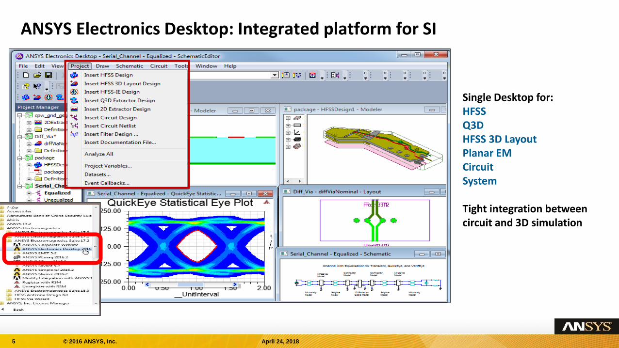
Single Desktop for:HFSSQ3DHFSS 3D LayoutPlanar EMCircuitSystem
Tight integration between circuit and 3D simulation
ANSYS Electronics Desktop: Integrated platform for SI

6 © 2016 ANSYS, Inc. April 24, 2018
• DesignXplorer is ANSYS powerful approach to explore, understand and optimize your engineering challenges for ANSYS Multiphysics analysis solvers, including electromagnetic.
Determine the key parameters influencing the design
Explore and understand the performance at other design or operating conditions
Find the conditions which give the best performance
Explore the robustness of the design
What is DesignXplorer?
Single Point What If?Response Surface
?
??

7 © 2016 ANSYS, Inc. April 24, 2018
DesignXplorer Features
What if StudyManual Search
Sensitivity / Correlation AnalysisFind the relevant parameters
Design of ExperimentsRun a smart set of Design Points
Response SurfaceBuild a Mathematical model
OptimizationWith or without a Response Surface
Robust DesignSix Sigma Analysis
Optimized and Robust Design

8 © 2016 ANSYS, Inc. April 24, 2018
Utilizing Design Space Exploration for Signal Integrity
Pre-layout what-if analysis

9 © 2016 ANSYS, Inc. April 24, 2018
• Differential stripline study with DesignXplorer
Pre-layout what-if analysis
• Optimization variables DK=8~10
DF=0.0013~0.0024
Width=50~80um
Seperation=1W~3W
Dielectric Thickness: 50~75um
Metal Thickness: 7~19um
Metal Conductivity: 0.67E7~1.5E7 Siemens/m
• Optimization goals
Characteristic Impedance: Z0 (differential) ~ 90 ohm
Minimize Insertion loss: >-3dB
Maximize Return Loss: <-10dB

10 © 2016 ANSYS, Inc. April 24, 2018
0 0
Port1
Port2
Port3
Port4
Trace1_in
Trace2_in
Input_ref
Trace1_out
Trace2_out
Output_ref
• Create a ANSYS Electronics Desktop project with Circuit Design in dynamic linked 2D Extractor
2D Extractor design: optimize impedance
Circuit Design: optimize insertion loss and return loss
Differential stripline model buildup

11 © 2016 ANSYS, Inc. April 24, 2018
DesignXplorer Response Surface Optimization setup
Input Variables
Optimization Goal

12 © 2016 ANSYS, Inc. April 24, 2018
Design of Experiments variable table generation
• Create Design of Experiments variable table
Specify design variable range setup
Preview the Design of Experiments variable table
Input variables
Optimization goals
DoE table

13 © 2016 ANSYS, Inc. April 24, 2018
• Once the Design of Experiments table is generated, run variable sweeping.
• DSO( Distribution Simulation Option) will distribute variables to multiple nodes to solve simultaneously.
Solve DoE table

14 © 2016 ANSYS, Inc. April 24, 2018
Sensitivity and Response Surface Plots
• Creating Sensitivity and Response Surface for the Design of Experiments results
Sensitivity will display the 2D sensitivity histogram of each input variables vers. output( Z0).
Response displays 3D interaction between variables vers. output ( Z0).
Trace_width, Trace_thickness and Top_die_thickness are top 3 sensitive variable for Z0.
Trace_width, Trace_thickness vs. Z0
Trace_width, Top_die_thickness vs. Z0

15 © 2016 ANSYS, Inc. April 24, 2018
• Specify the optimization objectives and constraints
Differential Characteristic impedance of 90 ohm with lower bound 85 ohm and upper bound 95 ohm
Maxmimum insertion loss
Minimum Return Loss
• The best benefit of the Response Surface approach in DesignXplorer is that the user can change the values of the cost and re-optimize with no further explicit simulations
Optimizing over the Response Surface

16 © 2016 ANSYS, Inc. April 24, 2018
• After you verify the candidate points, choose the best one for the design
IL&RL:
• Before optimization: Gray dot line
• After optimization: Red solid line
Differential Character Impedance:
• Before optimization: 49.5ohm
• After optimization: 84.3 ohm
Final Optimized results
Before optimization : After optimization:
Before optimization After optimization:

17 © 2016 ANSYS, Inc. April 24, 2018
Utilizing Design Space Exploration for Signal Integrity
Post-layout Optimization

18 © 2016 ANSYS, Inc. April 24, 2018
Package Socket PCB Vias Connector
CardPCB Package 2
RxTx
00 0 0 0 0 0 0
Port1 Port2
Port3 Port4
Port5 Port6
Port7 Port8
Port9 Port10
Port11 Port12
Port1
Port3
Port5
Port7
Port9
Port11
Port2
Port4
Port6
Port8
Port10
Port12
1
2
3
4
5
6
W241
Port1
Port3
Port5
Port7
Port9
Port11
Port2
Port4
Port6
Port8
Port10
Port12
Port1
Port3
Port5
Port7
Port9
Port11
Port2
Port4
Port6
Port8
Port10
Port12
1
2
3
4
5
6
W244
Port1
Port3
Port5
Port7
Port9
Port11
Port2
Port4
Port6
Port8
Port10
Port12
1
2
3
4
5
6
W246
1
2
3
4
5
6
W247
Port1
Port3
Port5
Port7
Port9
Port11
Port2
Port4
Port6
Port8
Port10
Port12
Port1
Port3
Port5
Port7
Port9
Port11
Port2
Port4
Port6
Port8
Port10
Port12
Port1:T1
Port1:T2
Port2:T2
Port2:T1
EMDesign1
Port1:T1
Port1:T2
Port2:T2
Port2:T1
EMDesign1
Port1:T1
Port1:T2
Port2:T2
Port2:T1
EMDesign1
Hierarchy PCIe Channel Example
Tx Rx
ID=194
ID=197
ID=198
ID=201
ID=202
Port1 Port2
Port3 Port4
Port5 Port6
Port7 Port8
Port9 Port10
Port11 Port12
LNA
HFSS model
Q2D Model HFSS3Dlayout model
System eye diagram analysis
Circuit LNA analysis
Component analysis

19 © 2016 ANSYS, Inc. April 24, 2018
PCIE Serial Channel Design Problem Scale
30 different factors are unreasonable considering an entire PCIe Channel, for example:
• Package
Thickness, Pad breakout, trace length, ball pitch, dielectric material (5)
• Socket
Thickness, material properties, SG via ratio (3)
• Board
MS and SL trace & space, etch factors, Cu roughness, dielectric materials, via config (8)
• Connector
Various vendor models, often only one or two options. (1)
• 2nd Board
MS, SL, etch factors, Cu roughness, dielectric materials, via config (8)
• 2nd Package
Thickness, Pad breakout, trace length, ball pitch, dielectric material (5)
If each factor has 4 variable value, the total combination scenario will be 120

20 © 2016 ANSYS, Inc. April 24, 2018
Different level variables combination affect different level character
• Sweeping variables‒ $FFE/DFE level on System level (Discrete distribution)
‒ $PCB_trace_length on Circuit level (Continues distribution)
‒ $anti_pad on Component level (Continues distribution)
• Optimization goal:‒ BER for statistic analysis
‒ Eye width/height for statistic/circuit analysis( timing domain)
‒ Insertion loss/Return loss for circuit analysis( frequency domain)

21 © 2016 ANSYS, Inc. April 24, 2018
PCIe Channel DoE data table
Simplified variable combination
scenarios to 50

22 © 2016 ANSYS, Inc. April 24, 2018
PCIe Channel Example – View the swept output
Differential IL with variables
Eye diagram with variables Bathtub with variables

23 © 2016 ANSYS, Inc. April 24, 2018
Response Surfaces
• Visualize response surfaces in 3D or 2D plots (continuous, discreet, mixed) variables
• The Measure of fit provides a metric for evaluating the accuracy of the response surface model.
• 3D: Eye Width vs. PCB tracelength& antipad size /Eye Width vs. FFE& Antipad size

24 © 2016 ANSYS, Inc. April 24, 2018
Sensitivity Plots
Sensitivity histogram shows that $Trace_length is the most
sensitive parameter for Eye_width

25 © 2016 ANSYS, Inc. April 24, 2018
Utilizing Design Space Exploration for Signal Integrity
Manufacture tolerance study (6σ-six sigma)

26 © 2016 ANSYS, Inc. April 24, 2018
• Differential stripline study with DesignXplorer
6σ analysis will be done based on user defined variable range and distribution
DesignXplorer for PCB manufacture tolerance study example
• Manufacture variables DK=8~10
DF=0.0013~0.0024
Width=50~80um
Seperation=1W~3W
Dielectric Thickness: 50~75um
Metal Thickness: 7~19um
Metal Conductivity: 0.67E7~1.5E7 Siemens/m
All variables are Normal (Gaussian) distribution

27 © 2016 ANSYS, Inc. April 24, 2018
6σ Analysis
6σ analysis is continuously studying, specifying each variable bounder and distribution.

28 © 2016 ANSYS, Inc. April 24, 2018
• 6σ analysis will give statically distribution function and relative sensitivity curve.
6σ Analysis results
The mean value was 48.79 ohm, peak value was 51.31ohm(min) and
68.47ohm( max)
Probability density distribution Relative Sensitivity results

29 © 2016 ANSYS, Inc. April 24, 2018
Full Hardware Utilization for Design Space Exploration

30 © 2016 ANSYS, Inc. April 24, 2018
• HPC enables increased productivity and higher fidelity simulation - including more geometric detail and larger systems.
• HPC helps you make your product development process, more productive and efficient.
• Faster turnaround and larger models all mean better designs in less time.
HPC: High Performance Computing
Faster
Higher Fidelity
Bigger

31 © 2016 ANSYS, Inc. April 24, 2018
How to Enable HPC Pool License ?
HPC = Faster• Tools > Options > HPC and Analysis Options
• Design Type:
• Specify more than 1 cores
• Options Tab– HPC License - Pool
Enable HPC Pool
Apple had 1536 tasks EM HPC workgroup license

32 © 2016 ANSYS, Inc. April 24, 2018
DSO: Distributed Solve Option
Distributed Solve Option
• Enables multiple parametric variations to be solved simultaneously on local and/or networked cores
• Each variable will utilize same HPC setting, which offers a near-linear speed-up with the number simultaneous variations (DSO tasks)
• Key for accelerating robust design (design of experiments, six sigma, etc.)
Distributed Solve
Option
Design Space Faster

33 © 2016 ANSYS, Inc. April 24, 2018
How to Enable DSO License ?
• Tools > Options > HPC and Analysis Options
HFSS, HFSS-IE and HFSS 3Dlayout:
• DSO is enable if check Use automatic settings
Q2D/Q3D, Maxwell, Circuit and Simplorer:
• In Job Distribution tab, checking OptimetricsVariations to enable DSO
HFSS, HFSS-IE, HFSS3Dlayout
Enable DSO
Q2D/Q3D, Maxwell,
Circuit, Simplorer
Enable DSO
Apple had 211 tasks DSO license

34 © 2016 ANSYS, Inc. April 24, 2018
• Software Requirements ANSYS Electronic Desktop 2016.2 (ANSYS EM Suite 17.2)
ANSYS Workbench 17.2 with Pre/Post
Integrated ANSYS Electronic Desktop with Workbench
• License ANSYS HFSS with SI options
Optimetrics
HPC
DSO
ANSYS DesignXplorer
Software and License requirements

35 © 2016 ANSYS, Inc. April 24, 2018
• ANSYS provides unified platform for Signal Integrity Design Space Exploration, which covers pre-layout, post-layout simulation and manufacture tolerance study.
• DesignXplorer gives easy way to automatically set up SI for Design Space exploration and Optimization
• HPC and DSO will utilize all of the available hardware to accelerate simulation.
Conclusion
Copyright © 2022 FDOKUMEN