Microfluidic Electrical Impedance Spectroscopy - CORE
72
MICROFLUIDIC ELECTRICAL IMPEDANCE SPECTROSCOPY A Thesis presented to the Faculty of California Polytechnic State University, San Luis Obispo In Partial Fulfillment of the Requirements for the Degree Master of Science in Biomedical Engineering by John J. Foley September 2018
-
Upload
khangminh22 -
Category
Documents
-
view
4 -
download
0
Transcript of Microfluidic Electrical Impedance Spectroscopy - CORE

MICROFLUIDIC ELECTRICAL IMPEDANCE SPECTROSCOPY
A Thesis
presented to
the Faculty of California Polytechnic State University,
San Luis Obispo
In Partial Fulfillment
of the Requirements for the Degree
Master of Science in Biomedical Engineering
by
John J. Foley
September 2018

ii
© 2018
John J. Foley
ALL RIGHTS RESERVED

iii
COMMITTEE MEMBERSHIP
TITLE: Microfluidic Electrical Impedance Spec-
troscopy
AUTHOR: John J. Foley
DATE SUBMITTED: September 2018
COMMITTEE CHAIR: Benjamin Hawkins, Ph.D.
Assistant Professor of Biomedical Engineering
COMMITTEE MEMBER: David Clague, Ph.D.
Professor of Biomedical Engineering
COMMITTEE MEMBER: Christopher Heylman, Ph.D.
Assistant Professor of Biomedical Engineering

iv
ABSTRACT
Microfluidic Electrical Impedance Spectroscopy
John J. Foley
The goal of this study is to design and manufacture a microfluidic device capable of
measuring changes in impedance values of microfluidic cell cultures. To characterize
this, an interdigitated array of electrodes was patterned over glass, where it was then
bonded to a series of fluidic networks created in PDMS via soft lithography. The
device measured ethanol impedance initially to show that values remain consistent
over time. Impedance values of water and 1% wt. saltwater were compared to show
that the device is able to detect changes in impedance, with up to a 60% reduction
in electrical impedance in saltwater. Cells were introduced into the device, where
changes in impedance were seen across multiple frequencies, indicating that the de-
vice is capable of detecting the presence of biologic elements within a system. Cell
measurements were performed using NIH-3T3 fibroblasts.

v
ACKNOWLEDGMENTS
Special thanks to:
• Benjamin Hawkins: For his hard work, dedication, time, and guidance
• David Lange: For his assistance in manufacturing processes and LabView code
• Kevin Wolfarth: For his assistance in microscopy and gradient validation
• My family and friends: For always being there as my support and counsel

vi
TABLE OF CONTENTS
Page
LIST OF TABLES...................................................................................................... viii
LIST OF FIGURES ........................................................................................... ix
CHAPTER
1 Introduction ................................................................................................. 1
1.1 Cell Culture and Analysis .................................................................... 1
1.2 Microfluidics ................................................................................................ 2
1.2.1 Definition and Overview .......................................................... 2
1.2.2 Advantages ............................................................................... 3
1.2.3 Disadvantages .......................................................................... 3
1.2.4 System Components ................................................................. 4
1.3 Impedance Spectroscopy ............................................................................. 4
2 Background .................................................................................................. 6
2.1 Fluid Properties ................................................................................... 6
2.1.1 Laminarity of Microflows ......................................................... 7
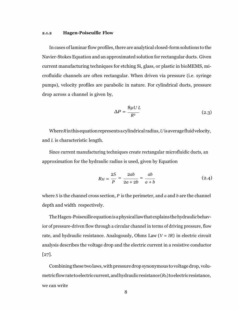
2.1.2 Hagen-Poiseuille Flow .................................................................... 8
2.1.3 Diffusion ................................................................................... 9
2.2 Concentration Gradient ....................................................................... 11
2.3 Electrical Impedance ........................................................................... 13
2.3.1 Parasitics .................................................................................. 14
2.3.2 Electrical Properties of the Cell ............................................... 15
2.3.3 Electric Double Layer ................................................................. 16
2.4 Manufacturing ..................................................................................... 18
2.4.1 Lithography .............................................................................. 18
2.4.2 PDMS and Plasma Bonding ..................................................... 19
3 Methods ....................................................................................................... 21
3.1 Microchip Design ................................................................................. 21
3.1.1 Design Considerations ............................................................. 23
3.2 Lithography: Creating the Mold .......................................................... 25
3.2.1 Characteristic Steps ................................................................. 25

vii
3.2.2 The First Layer: Alignment Marks ......................................... 29
3.2.3 The Second Layer: Shallow Channel Network ........................ 30
3.2.4 The Third Layer: Deep Channel Network ..............................30
3.3 Lift-off .................................................................................................. 32
3.3.1 Lithography .............................................................................. 32
3.3.2 Metal Deposition ..................................................................... 34
3.4 PDMS and Plasma Bonding ................................................................ 37
3.4.1 Fluid Connection ..................................................................... 38
3.5 Safety Concerns ................................................................................... 39
3.6 Device Data Collection ........................................................................40
3.6.1 Instrumentation .......................................................................40
3.6.2 Gradient Generator ................................................................. 40
3.6.3 Ethanol Control ....................................................................... 41
3.6.4 Saltwater .................................................................................. 41
3.6.5 Cell Injection ............................................................................ 41
4 Results/Discussion ...................................................................................... 43
4.1 Manufacturing: SU-8 Mold ................................................................ 43
4.1.1 Alignment ................................................................................. 43
4.1.2 Photoresist Spin ....................................................................... 43
4.2 Manufacturing: Electrode Array ........................................................ 44
4.2.1 Photoresist Spin ....................................................................... 44
4.2.2 Sputtering ................................................................................. 45
4.3 Characteristic Experiments ................................................................. 46
4.3.1 Concentration Generator ......................................................... 47
4.3.2 Impedance Measurements ...................................................... 49
4.4 Complications ...................................................................................... 52
4.4.1 Device Leaks ............................................................................ 52
5 Conclusions .................................................................................................. 54
5.1 Experiments......................................................................................... 54
5.2 Design Considerations ........................................................................ 55
5.3 Future Work ............................................................................................... 56
BIBLIOGRAPHY ............................................................................................... 58

viii
LIST OF TABLES
Table Page
2.1 Properties of PDMS .......................................................................... 20

ix
LIST OF FIGURES
Figure Page
1.1 Cell Presence in a Microchamber .................................................... 5
2.1 Laminar Flow ................................................................................... 7
2.2 Christmas-Tree Gradient Generator ............................................... 12
2.3 Ideal Impedance Measurement Circuit .......................................... 14
2.4 Parasitic Electronics ........................................................................ 15
2.5 Lipid Bi-layer Membrane ................................................................ 16
2.6 Electric Double-Layer ...................................................................... 17
2.7 PDMS Chemical Structure ............................................................... 20
3.1 Device Component Annotations ...................................................... 21
3.2 Gradient Generator Design ............................................................. 22
3.3 Cell Chamber and Cell Seeding Network Design ............................ 23
3.4 Fluid Delivery Network Design ....................................................... 24
3.5 Waste Collection Channel Design .................................................... 24
3.6 Interdigitated Microelectrode Array Design ................................... 25
3.7 Photoresist Spin Coater ................................................................... 26
3.8 CAD Drawing for Photomask .......................................................... 27
3.9 Photoresist Exposure to Ultraviolet Light ...................................... 28
3.10 Alignment Marking Photomask ......................................................30
3.11 10 µm Thick Microchannel Photomask .......................................... 31
3.12 60 µm Thick Microchannel Photomask .......................................... 32
3.13 Side-Wall Profile of Ma-N 1420 Photoresist ................................... 33
3.14 Electrode Array Photomask ............................................................. 34
3.15 Machines for Physical Vapor Deposition ........................................ 35
3.16 Immersion in Photoresist Strip ....................................................... 37
3.17 PDMS Processing ............................................................................. 37
3.18 Tygon Tubing Connections .............................................................. 39

x
4.1 Sputtering Adhesion ........................................................................ 45
4.2 Sputtering Errors ............................................................................. 46
4.3 COMSOL Concentration Simulation ............................................... 47
4.4 Food Dye Experiment ...................................................................... 48
4.5 Fluorescein Concentration Experiment .......................................... 49
4.6 Ethanol Control Experiment ........................................................... 49
4.7 Saltwater Impedance Comparison Experiment .............................. 50
4.8 Cell Injection Experiment………………………………………………………..51

1
Chapter 1 INTRODUCTION
1.1 Cell Culture and Analysis
When studying cellular behavior, whether in clinical diagnostics or academic re-
search, cells are cultured, grown, or treated within a platform, such as a petri dish,
culture flask, or bioreactor. Multiple methods have been developed for culturing,
separating, and analyzing cell cultures [25], affecting metrics such as cell number,
viability, and metabolite production for quantifying cell response to culture condi-
tions [33]. Advances in bio-technology cell research in the past decades have been
primarily in sterilization, materials, and the use of robotic automation to eliminate
manual pipetting, increasing throughput and accuracy. The advancements, however
have mainly enhanced test efficiency and accuracy and left much of the core of the
processes the same.
These conventional methods come with several inherent limitations. Macroscale
analysis is often labor-intensive and time consuming, and as the field of biotechnology
grows and increases the demand for cell-based diagnostics, these traditional methods
lack necessary throughput and make it difficult to quickly change and regulate cellular
environments. Single-cell and dynamic analysis are difficult and are often done with
conventional manual pipetting, decreasing accuracy and repeatability [25]. Further-
more, analysis of cellular components and the utilization of fluorescence-based dyes
are often destructive to the sample, hindering subsequent experimentation [21]. To
alleviate these limitations, we turn to the microscale, developing microfluidic plat-
forms and “lab-on-chip” devices. Combining a variety of engineering disciplines with
life science research, laboratory miniaturization hopes to reduce sample usage, cost,
and testing inaccuracy while increasing cell throughput.

2
1.2 Microfluidics
1.2.1 Deftnition and Overview
As the field of biotechnology continues to grow, larger numbers of experiments
for DNA analysis, point-of-care diagnostics, and drug development are needed. Just
as it transformed the world of electronics in the 1970’s, moving systems down into
the microscale has begun to transform the world of biotechnology as well [38]. Mi-
crofluidics is the field of study in which one manipulates fluids on the micron length
scale. Initially, microfluidic devices began with analytical methods of gas-phase chro-
matography, high-pressure liquid chromatography, and capillary electrophoresis. As
Cold War chemical threats and molecular biology genomics rose in the 1980’s and
90’s, microfluidic devices offered solutions for detection and DNA analysis spurring
a rapid growth of academic research [37]. The first microfluidic devices were fabri-
cated in silicon and glass in the 1990’s using lithography techniques adapted from the
microelectronics industry [38]. This incorporation of microelectromechanical systems
(MEMS) manufacturing and biologics gave rise to the bioMEMS industry and subse-
quently evolved the field of microfludics as well. With bioMEMS, more complex fluid
channel networks [28], valve flow controls [41], impedance detection [40], and even
devices capable of full laboratory protocols are now possible.
In recent years, “organ-on-a-chip” based microfluidics have been developed to re-
produce multiple physiological cell behaviorsin vitro. Models of the human lung [19],
liver [22], and kidney [26] have been realised in vitro through the usage of bioMEMS
and microfluidics. In many of these studies, device usefulness was characterized by
easily measured and observed functionalities. Practically, however, in vitro models
need to evaluate physiological responses to multiple biologic stimuli [18]. A microflu-
idic chip utilizing multiple culture wells could be one such approach to this limitation,
as it enables simultaneous cell studies under differing environmental conditions.

3
1.2.2 Advantages
Utilizing nanoliters or less of fluid at a time, microfluidic platforms offer potentially
higher throughput, lower cost per analysis, lower reagent and sample usage as well as
improved portability, sensitivity, and reliability. Traditional macroscale cell sorting
typically requires samples of 105 − 106 cells due to losses during setup and operation,
whereas microfluidic chips only need sample sizes in the 102 range [16]. Microvolumes
of sample allow for precise control of cell density, orientation, temperature, analyte
concentration, and dosage. The physical dimensions of a microfluidic device allow for
parallel experimentation on the same device and culture, enabling simultaneous cell
assays and analyses [25].
Polydimethylsiloxane (PDMS) is the most common substrate for microfluidic de-
vices. PDMS is optically transparent, non-conductive, elastic, and biocompatible.
This polymer allows for ease in cell culturing, simultaneous, fluorescent imaging, and
pneumatic valving.
Combining fluid mechanics, surface sciences, chemistry, biology, and often optics,
electronics, and control systems areas of research, microfluidics has a great potential
to impact a variety of industries such as pharmaceuticals, bio-defense, public health,
point-of-care diagnostics, and agriculture.
1.2.3 Disadvantages
Constructing a device out of PDMS certainly has drawbacks. PDMS is hydropho-
bic in nature, leading to an adsorption of hydrophobic molecules (such as lipids) from
culture media and resist aqueous fluid flow. PDMS is also porous, causing minor gas
and water permeability. To alleviate these issues, PDMS is often surface treated [25]
or designed around.

4
While the field of microfluidics possess great potential to impact multiple inter-
disciplinary fields, microfluidic devices in general also come with several drawbacks.
While microfluidic analyzers may have lower cost per analysis, the barrier-to-entry
financially in this field is quite high. Commercial microfluidic device production cur-
rently requires clean room accessibility, often costing millions of dollars. Research,
development, and resources for systems can be quite expensive compared to conven-
tional counterparts. Furthermore, while the microfluidic chip itself might be space
efficient, additional data acquisition hardware and power requirements (such as pump-
ing mechanisms) can quickly turn a “lab-on-a-chip” into a “chip-on-a-lab”.
1.2.4 System Components
A modern microfluidic system is comprised of a variety of components: a method
for moving or manipulating fluids, a series of delivery and channel networks, a cham-
ber for analytes, and a modality for analytic techniques. These sub-systems can be
internally integrated with the chip or externally sourced. The issue with internal
integration is the increased design complexity of creating and interfacing these sub-
systems all with millimeter and sub-millimeter constraints. Power requirements, heat
generation, cost, precision, and manufacturing difficulties need to be addressed for
internal system components. The issue with external sourcing of sub-systems is an
issue with size or portability. Using external pumps, sensors, and analytic software
creates a microchip that needs an entire workbench to operate.
1.3 Impedance Spectroscopy
Impedance spectroscopy is a method of analysis that uses electrical impedance
measurements to characterize various system properties. Within microfluidic cell
research, impedance spectroscopy can be used to quantify cell population change,

5
fluid properties, or other changes in the cellular environment. For example, cell
proliferation across electrodes should increase the overall system’s complex impedance
(equivalent circuit shown in Figure 1.1). Using these changes in impedance based on
cell population, we can study how changes in cellular environments can influence cell
growth. These impedance changes due to the presence of cells can be measured to
quantify cells present in the system.
Figure 1.1 Cell Presence in a Microchamber: Image redacted from Figure 1 of Gawad et al. “Micromachined Impedance Spectroscopy Flow Cytometer for Cell Analysis and Particle Sizing” [13]. Please see source for full image
The principle of impedance spectroscopy was first demonstrated during fibroblast
monitoring with an applied electric field in 1984 [14] and since then, impedance
measurements of cell response and behavior have been made across interdigitated
microelectrode arrays [11, 3]. In 2004, Radke used impedance spectroscopy to detect
Escherichia coli in samples [29, 30] and was able to make detections within 5 minutes.
Recently, Rother et al. utilized impedance sensing to determine electromechanical
connectivity between mammalian fibroblasts and cardiomyocytes [20].
While highly variable depending on electrode surface area, external circuitry, cell
count, cell type, growth media, etc., one would expect higher overall impedance due
to the cell’s added capacitance on the system at-large.

6
Dt
Dt
Chapter 2 BACKGROUND
We are interested in developing a microfluidic chip to measure cell impedance
based on varying system environments. To that end, it is important to consider
factors such as fluid properties within a microchannel, pressure-based flow, diffusive
transport, the electric double layer, cell membrane impedance, and various micro-
electro-mechanical (MEMs) manufacturing techniques.
2.1 Fluid Properties
When developing a microfluidic system from the ground-up, it is important to con-
sider the governing physics that influence design and system behavior. The following
section will discuss various fluid properties that need to be considered in microfluid
design.
Many characteristics governing microfluids are based on the macroscopic approach
of continuum mechanics, that in every elementary volume of fluid there exist sufficient
molecules to define fluid properties of interest, such as pressure, density, viscosity,
specific heat, and temperature.
The Navier-Stokes Equation represents the conservation of momentum at any
given fluid point [4]. In three-dimensional vector notation, the Navier-Stokes equation
can be written as follows.
ρ
Dv = −∇ P + µ∇ 2v + F
(2.1)
Where ρ is density, v is fluid velocity, P is pressure, µ is fluid viscosity, Dv
is the
time rate of change of a moving fluid, and F is the vector sum of applied forces.
Note that Equation 2.1 assumes that fluid is incompressible and Newtonian.
These assumptions are viable for water at 20 C under laminar flow [4].

7
2.1.1 Laminarity of Microflows
Fluid flow behavior is characterized by the ratio of viscous forces to inertial forces.
When inertial forces dominate, flow becomes turbulent and random fluctuating vor-
tices are allowed to develop. When viscous forces dominate, fluid flow lines become
locally parallel and the fluid exhibits laminar flow. The laminarity of fluid flow is
characterized by the dimensionless Reynold’s number:
U D Re =
ν
(2.2)
Where U is average fluid velocity, D is characteristic length, and ν is the fluid’s
kinematic viscosity.
Figure 2.1 Laminar Flow: A sphere in Stoke’s flow under very low Reynold numbers. [9]
Figure 2.1 demonstrates flow profiles with small Reynold’s numbers (<0.1). While
turbulence is of consideration with macroscale fluid networks, microfluid channels
often exhibit these laminar flow profiles, regardless of channel geometry. Owing to
the characteristic length-scales and typical microfluidic flowrates, Reynold’s numbers
typically range between 10-4 and 1 [4].
8
2.1.2 Hagen-Poiseuille Flow
In cases of laminar flow profiles, there are analytical closed-form solutions to the
Navier-Stokes Equation and an approximated solution for rectangular ducts. Given
current manufacturing techniques for etching Si, glass, or plastic in bioMEMS, mi-
crofluidic channels are often rectangular. When driven via pressure (i.e. syringe
pumps), velocity profiles are parabolic in nature. For cylindrical ducts, pressure
drop across a channel is given by,
∆P = 8µU L
R2 (2.3)
Where R in this equation represents a cylindrical radius, U is average fluid velocity,
and L is characteristic length.
Since current manufacturing techniques create rectangular microfluidic ducts, an
approximation for the hydraulic radius is used, given by Equation
2S 2ab ab RH = = = (2.4)
P 2a + 2b a + b
where S is the channel cross section, P is the perimeter, and a and b are the channel
depth and width respectively.
The Hagen-Poiseuille equation is a physical law that explains the hydraulic behav-
ior of pressure-driven flow through a circular channel in terms of driving pressure, flow
rate, and hydraulic resistance. Analogously, Ohms Law (V = IR) in electric circuit
analysis describes the voltage drop and the electric current in a resistive conductor
[27].
Combining these two laws, with pressure drop synonymous to voltage drop, volu-
metric flow rate to electric current, and hydraulic resistance (Rh) to electric resistance,
we can write

9
∆P = QRh (2.5)
While this analogy does not provide any information about velocity profiles or
flow patterns, it does provide an excellent simplification to complicated microfluidic
networks and necessary values such as maximum flow rates, pressure limits, and
hydraulic resistances.
2.1.3 Diffusion
In simple fluids, a molecule will travel in a straight line until it collides with
another molecule and changes direction. This distance until collision is known as the
mean free path. Looking at a single molecule, it will continue to shift directions as
it collides with other molecules. The path of this molecule over time is known as a
particle’s random walk or Brownian motion [4].
This concept of Brownian motion, first discovered by J. Ingenhousz and R. Brown,
forms the basic principle for diffusion. Each particle within a fluid exhibits this ran-
dom walk effect. Over enough time, the average net displacement of each particle
will have evenly dispersed throughout a given volume. This dispersion towards equi-
librium is the phenomena of diffusion.
Fick’s 1st Law relates a solute’s mass flux to its concentration gradient
J = −D∇ c (2.6)
where D is the solute’s diffusion coefficient. Using Fick’s 1st Law and conservation
of mass, we can write Fick’s 2nd Law:
∂c = D∆c + S (2.7)
∂t
where ∆ c is change in analyte concentration.

10
c ∂x ∂y ∂z
The driving force behind diffusion is written as
1 ∂µ ∂µ ∂µ
FDiffusion = − N
( + + ) (2.8) ∂x ∂y ∂z
where NA is Avogadro’s number and µ is the chemical potential of the analyte:
µ = µ0 + RTln(γc) (2.9)
Where R is the gas constant, T is temperature in Kelvin, γ is the specific weight
of the fluid, and c is the analyte’s concentration.
We can then obtain
F
= −
kBT(
∂c +
∂c +
∂c ) (2.10)
which FDiffusion = FFriction = CDv, where CD is the friction factor and v is the
stationary velocity. Thus
v = − kBT
( dc
+ dc
+ dc
) (2.11) CDc dx dy dz
Comparing this to Ficks’s Law, we obtain
D = kBT
CD
(2.12)
where D represents a solute’s diffusion coefficient, a key property in the design of
diffusion-based fluid systems. For a sphere, we can use Stoke’s drag, or CD = 6πµa.
Transport Phenomena
In microfluidics and biotechnology, manipulation of target analytes such as DNA,
proteins, cells, drugs, etc. is a key functionality of the device. Knowledge of trans-
Diffusion
A

11
port phenomena within this space is necessary when designing a microfluidic device.
Dependent of fluid velocity, microchannel dimensions, and the particles diffusion co-
effecient (derived in section 2.1.3), transport of an analyte is dictated by diffusive
and convective means, with the most dominant mechanism characterized by the mass
transport Peclet number, a dimensionless variable that gives the ratio of diffusive to
convective flux. U A
P e = D
(2.13)
where A is the characteristic length of the microchannel, U is the average fluid
velocity, and D is the diffusion coefficient from Equation 2.12.
A Peclet number less than 1 signifies that diffusion is the dominant mode of
particle transport within the fluidic network. When this occurs, it is important to
consider the time scale required for two fluids within a microchannel to reach steady-
state equilibrium.
A2
t = 2D
(2.14)
Using Equation 2.14, with a known fluid velocity, one can determine the charac-
teristic mixing length A needed for fluids to reach equilibrium. If equilibrium does
not occur during mixing, incorrect concentrations will develop, negatively impacting
results.
2.2 Concentration Gradient
A concentration gradient generator is capable of generating a wide range of con-
centrations. This network and concentration gradient is essential to the study of
fluidic chemical properties and how they impact overall cell response. Microfluidics
can be used to lower the time and space requirements to generate specific gradients,
enabling simultaneous studies of multiple cellular environments and their respective
responses to differing analyte concentrations [35].

12
Concentration gradients are necessary for a variety of biologic processes, such as
development, immune response, and wound healing. While macroscale approaches
could be used to generate these gradients even at the single-cell level, length scales in
the microenvironment are on the order of microns, providing better gradient resolution
and higher degrees of fluid control. With such small diffusive length, both channel
lengths and time-to-dose are reduced as well.
Jeon et. al created a “Christmas tree” gradient generator and used it to deliver
incrementally increasing concentrations of hydrofluoric (HF) acid to etch glass pro-
portionally to the concentration of HF [10]. This gradient design has since been
adopted in studies on chemical effects on cells [5],[31] and chemotaxis bacterial stud-
ies [12],[36]. An example of Jeon’s Christmas tree generator is shown in Figure 2.2.
When designing a gradient generator, primary considerations are appropriate dif-
fusive mixing lengths (based on fluid velocity and the diffusivity coefficient) and the
total number of final mixing branches (for example in Figure 2.2, this generator will
produce a gradient of 9 distinct concentrations). Using the aforementioned circuit
analogy in subsection 2.1.2, concentration gradient channel dimensions can be eas-
ily designed without the use of complex simulations or additional experimentation.
Figure 2.2 Christmas-Tree Gradient Generator: Red represents high analyte con- centration, whereas blue represents low concentration.

13
jωC
Starting from the inlets, just like electrical current, flow rates are proportional
to the summation of downstream resistance. Equalizing hydraulic resistance across
all respective fluidic networks will cause an even flow distribution between each
cell chamber.
2.3 Electrical Impedance
Impedance is a measurement of a circuit’s resistance to current flow due to an
applied voltage as a function of frequency. Using an alternating current (AC) voltage
source, impedance becomes a complex value that combines resistive, capacitive, and
inductive effects within a circuit, shown by Equation 2.15.
Z = R + jX (2.15)
where Z is overall impedance, R is real resistive effects, and X is reactance,
denoted by j, implying that this value is “imaginary”.
The amount of capacitance within a circuit is a frequency dependent value denoted
by ZC = 1 . Impedance due to capacitance is inversely proportional to frequency.
When looking at the phase angle in AC circuit analysis, capacitance has a negative ef-
fect on phase angle. Inductance within a circuit is denoted by ZL = jωL. Impedance
due to inductance is directly proportional to rises in frequency. Inductance has a
positive effect on phase angle, and when combined with capacitance, positive phase
indicates stronger inductive effects, whereas negative phase indicates stronger capac-
itive effects.

14
When measuring impedance, two oscilloscope probes are placed across the device
under test (DUT). Current flows through the device, with relative voltage drop across
the device being compared to voltage across an external resistor in the circuit. A fre-
quency sweep is performed to measure the device’s overall impedance across multiple
frequencies. A basic impedance measurement setup can be shown in Figure 2.3.
Figure 2.3 Ideal Impedance Measurement Circuit: Circuit for measuring system impedance under ideal conditions
2.3.1 Parasitics
No electronic system behaves in an ideal fashion. In every system, parasitic ele-
ments influence realistic measurements from their theoretical solutions. Node connec-
tions, such as clips, circuit boards, and breadboards can exhibit parasitic capacitance.
Long or coiled wires from oscilloscopes and probes exhibit parasitic inductance. Even
internal electronics from power supplies and computer systems add to a system’s
overall impedance. Depending on one’s experimental setup, large parasitic elements
in a system can significantly impact measurements by adding noise and reducing the
system’s overall sensitivity to variations in impedance. Adding parasitic elements
into Figure 2.3, we see that a realistic circuit model looks closer to Figure 2.4.
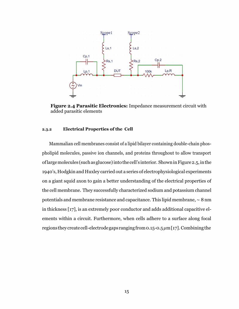
15
Figure 2.4 Parasitic Electronics: Impedance measurement circuit with added parasitic elements
2.3.2 Electrical Properties of the Cell
Mammalian cell membranes consist of a lipid bilayer containing double-chain phos-
pholipid molecules, passive ion channels, and proteins throughout to allow transport
of large molecules (such as glucose) into the cell’s interior. Shown in Figure 2.5, in the
1940’s, Hodgkin and Huxley carried out a series of electrophysiological experiments
on a giant squid axon to gain a better understanding of the electrical properties of
the cell membrane. They successfully characterized sodium and potassium channel
potentials and membrane resistance and capacitance. This lipid membrane, ∼ 8 nm
in thickness [17], is an extremely poor conductor and adds additional capacitive el-
ements within a circuit. Furthermore, when cells adhere to a surface along focal
regions they create cell-electrode gaps ranging from 0.15-0.5 µm [17]. Combining the

16
Figure 2.5 Lipid Bi-Layer Membrane: a) Representative picture of the various components of the cell mem- brane [6]. b) Hogkin-Huxley model of the electrical characteristics of the cell mem- brane [8]. EL and En are the Nernst potentials for respective ion channels. gn, and gL are the conductive elements for respective ion channels. I is a current traveling along the cell membrane, and C is the overall capacitance of the lipid bilayer.
capacitive membrane and adhesion gap with resistive cell elements (such as the nu-
cleus in the cytoplasm), the presence of cells between electrodes should influence the
overall impedance of the system.
2.3.3 Electric Double Layer
The electric double layer is an interface region formed whenever an electrode is
immersed in an electrolytic solution. Functioning similar to a capacitive element, it is
important to consider the electric double layer effects on the overall system impedance.
Electrical properties and structure of this layer depend on a variety of factors, such
as electrode material, surface oxides, surface area, solvent type, electrolyte type, and
temperature [34].
In 1879, Helmholtz put forth the first model of the electric double layer [34]. This
model assumed there existed a compact layer of ions in contact with the charged
metal surface. Later, Gouy and Chapman suggested that this compact layer was in
fact a diffuse layer of ions that extends some distance away from the metal surface,
according to a Boltzmann distribution [34]. In 1924, Stern suggested that the interface

17
contains both a rigid Helmholtz layer and a diffuse Gouy-Chapman one. In the 1950’s
and 60’s, the role of the solvent was taken into account, and it was found that polar
solvents, such as water, also interact with the charged metal surface [34].
Figure 2.6 Electric Double-Layer: structure created by negatively charged metal surface [7]
Shown in Figure 2.6, the electric double layer consists of two planes. The first, the
inner Helmholtz plane, consists of specifically adsorbed ions, located behind the layer
of adsorbed water molecules. This inner plane represents the original rigid Helmholtz
layer. The second, the outer Helmholtz plane, consists of hydrated ions in contact
with the electrode surface. The diffuse layer develops beyond the outer plane, with
ionic concentrations and potential decreasing exponentially with distance from the
electrode [34].
While the impedance effects of the electric double layer in this project were not
theoretically quantified, they are present in the system. Therefore, impedance mea-
surements can be calibrated to a baseline measurement before and after biologic
introduction.

18
2.4 Manufacturing
2.4.1 Lithography
Lithography, invented in 1959, has been paramount for developing modern elec-
tronics and is the foundation for all integrated circuits. In the 1970’s, lithography
became commonplace in the semiconductor industry [39] and has since caused the
field to expand exponentially, primarily in the field of smartphones and computer
processors.
Derived directly from the microelectronics industry, manufacturing microfluidic
platforms use this same process of lithography. It has enabled the smaller feature
sizes and aspect ratios needed for fluidic networks. Photoresist, a photo sensitive
polymer suspended in solvent, is spun onto a silicon wafer, typically 1-10 µm thick.
Exposure of the photoresist layer to ultraviolet light alters its solubility, allowing
specific patterns to be transferred via a photomask [15]. The activated photoresist
is then chemically removed using a developer solution, revealing the desired pattern
transferred during UV exposure. Multiple layers of photoresist can be spun and
exposed, then developed via a single development step [23].
SU-8 is a high contrast, negative-tone, epoxy-based photoresist that has gained
much popularity for exploratory microfluidics. Upon exposure, SU-8 forms internal
cross-links that prevent removal during development. This process creates a three-
dimensional microstructure of the photoresist on the surface of the wafer. In microflu-
idics, this structure serves several purposes. The first is usage as a negative mold to
create necessary microchannel networks in a process called soft lithography. PDMS
(polydimethyl siloxane) is mixed, poured, and cured over the microstructure mold.
Channel networks are formed into the PDMS surface, which is then removed from
the wafer, oxidized via plasma and bonded to another substrate. The second purpose

19
involves a process known as lift-off. The microstructure serves as a protective layer
during metallic sputtering [15]. Gas, typically argon or oxygen, is ionized and bom-
bards a metallic target, releasing particles that then coat the photoresist and silicon
wafer. The photoresist blocks metal from adhering to the silicon in specified areas.
Upon chemical removal of the photoresist (lift-off), metal traces are left in areas of
bare silicon during sputtering. These metal traces can form a series of interdigitated
electrodes that can be placed alongside a fluidic network, creating a microscale device
capable of measuring changes in impedance due to the system properties.
2.4.2 PDMS and Plasma Bonding
Early microfluidic platforms analyzing aqueous solutions were manufactured out
of silicon and glass using conventional lithogrpahy adapted from the microelectron-
ics industry[38]. Manufacturing these devices was expensive, time-consuming, and
required highly specialized clean room environments, counter to the overall goals of
microfluidics.
Polydimethylsiloxane, better known as PDMS, an organic silicone polymer, has
gained large popularity in exploratory microfluidics research. PDMS has an intrinsicly
hydrophobic surface consisting of repeating –O-Si(CH3)2– groups. While hydrophobic
materials are generally a poor choice for aqueous solution analytics, exposure to
oxygen plasma creates surface silanol (Si-OH) groups and destroys methyl (Si-CH3)
groups, creating a temporary hydrophilic surface that can be properly wetted by
aqueous solutions and polar solvents. These silanol groups can be further modified to
create permanent hydrophilic surfaces, reduce nonspecific protein adhesion, or create
cross-links for specific protein attachment [2]. A listing of relevant PDMS properties
can be found in Table 2.1.
Irreversible seals can be formed between PDMS and PDMS, glass, silicon, polystyrene,

20
Figure 2.7 PDMS Chemical Structure: a) Chemical structure of PDMS. b) Chemical structure of PDMS after plasma oxidation [32]
polyethylene, or silicon nitride. When these materials are oxidized, polar –OH func-
tional groups form covalent –O-Si-O– bonds with oxidized PDMS silanol groups,
creating a bond stronger than the intrinsic bonds of PDMS itself. Keeping surfaces,
dry, clean, smooth, and load-free during plasma bonding and a 70C post-oxidation
bake can greatly improve seal strength [24].
Table 2.1: Properties of PDMS [24]
Property Characteristic Effect
Optical Transparent w/ UV cutoff of 240 nm
Optical usage between 240 and 1100 nm
Electrical Insulating, breakdown volt- age of 2x10⁷ V/m
Allows for integrated circuitry
Mechanical Elastomeric, Young’s modu- lus ∼750 kPa
Surface conformation; reversible de- formation allows for pneumatic actu- ation
Interfacial Low surface free energy, ∼20 erg/cm2
Replicas easily removed from molds; hydrophilic surface when oxidized (SiOH functional group)
Permeability Low permeability to liquid water; permeable to gases and nonpolar organic sol- vents
Channels maintain aqueous solu- tions; gas transport allowed through bulk; many organic solvents are in- compatible
Reactivity Inert; plasma exposure will oxidize surface
Unreactive with most reagents, sur- face can be modified to be hy- drophilic and reactive to silanes
Toxicity Nontoxic Can be implanted in vivo; allows for mammalian cell growth

21
Chapter 3 METHODS
3.1 Microchip Design
Figure 3.1 represents a CAD outline of the two device footprints, the fluid channel
networks and the microelectrode array pattern. The annotations in red can be used
to identify various components of the device as discussed in the following sections.
Figure 3.1 Device Component Annotations: Device footprint in CAD with annotations of various components in red. Top: Fluid channel network. Bottom: Microelectrode array pattern.
The microchip was designed to generate sixteen different solute concentrations
across sixteen respective cell chambers. Within these chambers, a microelectrode
array was patterned across each chamber base to measure the chamber’s overall
impedance, and, depending on differing solutes and/or biologics, measure changes
in impedance.

22
To generate a gradient of sixteen differing concentrations, Jeon’s Christmas tree
style was adopted. Gradient channels were designed to be 50 µm in width, 10 µm in
depth, and each “mixer” to have a characteristic mixing length of 6 mm to ensure
fluids have reached a diffusion equilibrium before the next mixing. Gradient generator
design for this device is shown in Figure 3.2.
Figure 3.2 Gradient Generator Design: a) Full design for gradient generator b) Single characteristic mixer channel
Shown in Figure 3.3, cell chambers were designed to be 5 mm in diameter, 60
µm in depth, and contain an array of posts 75 µm in diameter. These posts were
designed to provide structural support due to the cell chamber’s low aspect ratio
(width height). A cell seeding network was placed between cell chambers (Figure
3.3) to allow cell injection prior to treatment. Channels were 75 µm wide and 60 µm
in depth and were added to create a one-way path for cells throughout each of the
chambers.
Fluidic networks, shown in Figure 3.4, into and out of the cell chamber were
designed to be 75 µm in width and 10 µm in depth. The height difference between
the fluidic network and the cell chamber is intended to prevent cell growth up the
fluidic network by creating unfavorable cell growth conditions due to increased flow
rate and wall shear in the delivery channels.
Cell waste collection, shown in Figure 3.5, begins at the end of the fluidic net-

23
works and provides a universal collection channel, needing only one outlet port in
the microchip. This channel is 200 µm in width and 60 µm in depth to minimize its
Figure 3.3 Cell Chamber and Cell Seeding Network Design:
Characteristic image of cell chamber and seeding network
impact on the overall fluidic resistance of the device.
The microelectrode array, shown in Figure 3.6, consists of an array of interdigi-
tated electrodes 25 µm in width and spaced 25 µm apart. Larger gaps in the inter-
digitation were created to allow for potential microscopy quantification.
3.1.1 Design Considerations
Multiple factors such as material properties, manufacturing constraints, and ex-
perimental conditions must be taken into account during the design of the microchip.
Minimum feature size with SU-8 photolithography and available resources was 10
µm. While constructing feature sizes at this length scale is possible, it increases the
likelihood of error and reduces feature quality (eg., rounded edges or discontinuities).
To avoid this, no geometries were designed under 10 µm. SU-8 material properties

24
constrained maximum channel to depth to 100 µm.
Because the channels are shallow, a dimension width of less than 250 µm was
Figure 3.4 Fluid Delivery Network Design: Characteristic fluid path to cell chambers
Figure 3.5 Waste Collection Channel Design: Characteristic cell waste collection network
observed to minimize “bowing” of the channel ceiling due to the weight of PDMS
itself. Due to leaching and minor permeability of PDMS, no features were placed
within 50 µm of another to avoid any potential diffusion through PDMS. Furthermore,
the maximum allowable footprint of the device was 25 mm by 75 mm, as it was
manufactured on a microscope slide to allow for potential microscopy.

25
Figure 3.6 Interdigitated Microelectrode Array Design: a) Electrode arrays and bond pads b) Characteristic electrode array
3.2 Lithography: Creating the Mold
3.2.1 Characteristic Steps
The following section contains a general overview of the steps required in soft
lithography. More details for each lithography process used can be found in later
sections.
The first step in lithography is to clean the substrate. A silicon wafer was used
as a flat, non-porous substrate for the photoresist mold. Wafers were first cleaned
in piranha, a 9:1 mixture of 98 v/v % sulfuric acid and 30 v/v% hydrogen peroxide,
at 70C for 10 minutes. This is done to remove any organics potentially present on
the wafer’s surface. The wafers were then dipped in buffered oxide etch (BOE), a
mixture of hydrofluoric (HF) acid and water, at room temperature for 1 minute. This
is to remove any native oxide growth on the wafer’s surface. Wafer’s were placed in a
spin-rinse-dry (SRD) tool to remove potential residual acids. A dehydration bake is
then done at 150C for 5 minutes on a hot plate to drive-off water from the surface.
This is done as residual moisture will prevent photoresist adhesion to the silicon’s
surface.
The second step is to spin-on the photoresist. Using the Laurell spin coater shown

26
in Figure 3.7, four milliliters of photoresist were poured over the wafer’s surface and
placed under vacuum. A slow spin speed was initially used to spread the resist evenly
across the wafer surface. The spin speed was then increased to match the desired
layer thickness according to the manufacturer’s datasheet. The spin speed was then
lowered to reduce stresses introduced to the photoresist during the high spin cycle. It
is important to note that defects in the resist, such as poor adhesion or air bubbles,
can be “reset” by immersing the wafer in acetone and rinsing with isopropyl alcohol
and deionized water, then repeating the cleaning process from start. Post-spinning,
the photoresist forms a thick layer on the edge due to its viscosity. This so-called
edge-bead layer causes issues during exposure, and is removed by using a razorblade
to and wipe the outermost surface edge.
Figure 3.7 Photoresist Spin Coater: Spin coat machine used to
spin-on various layers of photoresist
The third step is to soft-bake the wafer. This is done to evaporate solvent and
promote thermal stability. Wafers were placed on a hot plate at 65C and increased to
the desired temperature for the resist (95 - 100C) for approximately 2 minutes. The

27
temperature was then passively cooled down to 65C and then to room temperature.
This temperature ramp cycle is done to minimize thermal stresses on the photoresist
layer.
The fourth step is ultraviolet (UV) exposure. A two-dimensional CAD drawing
(Figure 3.8) of the microchip was sent to CAD/Art Services, where it was then sep-
arated into separate layers and printed on mylar sheets with 20,000 dpi resolution.
This mylar photomask serves as a protective layer against UV exposure to the pho-
toresist. Three layers were used for the SU-8 master mold: alignment marks, the 10
µm thick microchannels, and the 60 µm thick microchannels. A fourth photomask
was used in a later process to pattern the electrode array as well.
Figure 3.8 CAD Drawing for Photomask: CAD File used for mylar photomask production

28
Figure 3.9 Photoresist Exposure to Ultraviolet Light: Wafer during UV exposure
Figure 3.9 shows a wafer covered by a mylar photomask undergoing UV exposure.
Wafers were placed 10 µm away from the respective mylar photomask and glass plate.
Exposure dosage was set to 15 mW/cm2 with an h-line mercury arc lamp. Exposure
times varied based on the resist itself and its layer thickness. Most of the photoresists
used in this process are negative-tone resists, meaning that UV exposure forms cross-
links within the resist, rendering it insoluble to the developer solution. This step
forms the desired pattern from the photomask onto the photoresist.
The fifth step is a post-exposure bake (PEB). A similar process to the post-spin
soft-bake, a PEB is done to reinforce the cross-links created during UV exposure.
Patterns should become visible during this step. While some resists do not require
this step, failure to do so when needed will remove all photoresist from the surface,
not just the areas of interest.
The final step is development. Developer solutions used were the those
premade by the photoresist manufacturer. In the case of negative-tone resists,

29
unexposed areas are removed during this process. Development times are highly
variable based on resist type, layer thickness, and developer age, with manufacturer
datasheets used for estimates. Wafers were immersed and slightly agitated within
the developer for the allotted time. Upon removal, they were rinsed with isopropyl
alcohol and/or deionized water. If a milky-white resist was present on the surface
during the rinse, the wafers were immersed in developer in 30 second increments
until a clean rinse was achieved. The wafers were then spin-rinsed-dried and set
for storage.
3.2.2 The First Layer: Alignment Marks
Before photoresist spin-on, the wafers were placed in an oxidation furnace at
1100C to grow a thin uniform layer of oxide over the wafer’s surface. The first
layer of the photoresist aids in creation of the alignment structure. For this, AZ-
1529 was used instead of SU-8, as SU-8 is not easily removed. AZ-1529, unlike SU-8,
is a positive-tone resist, meaning that UV exposure renders it soluble to developer
solution. Four milliliters of resist was poured over the wafer and spun-on at 400 rpm
for 15 seconds to spread the resist evenly, then increased to 3000 rpm for 30 seconds
and a 300 rpm 10 second spin. The resist was then exposed to the first photomask:
the alignment layer, as depicted in Figure 3.10. After being developed in CD-26, a
developer by MicroChem, resist was removed in specified areas.
This process left photoresist over the surface oxide at the alignment marks. The
wafer was then dipped in BOE for 5 minutes to remove the oxide, with the photoresist
serving as a protective layer during removal, leaving oxide structures to serve as
the alignment layer. An oxide was chosen for this layer as it provided the greatest
optical contrast in future alignment steps. The wafer was then spin-rinsed-dried and
dehydration baked in preparation for the next photoresist layer.

30
Figure 3.10 Alignment Marking Photomask: Mylar photomask used for the first layer of AZ-1529 photoresist. Pat- terns the alignment marks used for future resist layers.
3.2.3 The Second Layer: Shallow Channel Network
The second layer of photoresist serves as the 10µm thick mold for microchannels.
The layer will form the concentration gradient and fluid networks to and from the cell
chambers. SU-8 2007, a negative-tone photoresist by MicroChem, was used for this
layer. The resist was removed from refrigeration and brought to room temperature,
then was spun-on to the surface at 200 rpm for 25 seconds, 500 rpm for 10 seconds,
1500 rpm for 30 seconds, and 300 rpm for 10 seconds for a target 10µm thick layer.
After edge bead removal, the wafer was soft-baked at 95C for 2 minutes and 30
seconds, with a temperature ramp starting from 65C to reduce thermal stresses.
The wafer was exposed to the second photomask layer (Figure 3.11) for 8.3 seconds
using the oxide alignment marks for guidance. This layer does not get developed until
after the next layer of photoresist.
3.2.4 The Third Layer: Deep Channel Network
The third layer of photoresist serves as the 60µm thick mold for microchannels.
This layer will form the cell seeding network, the cell chambers, and the waste collec-
tion network. SU-8 2050 was used for this layer, as its higher viscosity compared to

31
Figure 3.11 10 µm Thick Microchannel Photomask: Mylar photomask for the SU-8 2007 layer. Patterns the gradient generator and fluid networks
SU-8 2007 allows for thicker channel geometries. The wafer was soft-baked at 95C for
6 minutes, using appropriate 65C temperature ramps as well. After being exposed
to the third photomask layer (Figure 3.12) for 11.4 seconds, the wafer was developed
in MicroChem’s SU-8 developer for 6 minutes, removing unexposed SU-8 2007 and
SU-8 2050. Isopropyl alcohol was used to clean the developer solution, where the
wafer was then rinsed with deionized water, and spin-rinse-dried.

32
Figure 3.12 60 µm Thick Microchannel Photomask: Mylar photomask for the SU-8 2050 layer. Patterns the cell seeding network, cell chambers, and waste collection
3.3 Lift-off
3.3.1 Lithography
A glass wafer was used as the substrate for the lift-off process. Due to its trans-
parency, patterning the microelectrode array over glass allows for the ability to take
microscopy measurements if needed. The wafer was first cleaned in piranha at 70C
for 10 minutes and buffered oxide etch (BOE) for 30 seconds. After a spin, rinse, and
dry, the wafer underwent a dehydration bake at 200C for 10 minutes.
The photoresist ma-N 1420 by MicroChem was used for this process. This resist
was chosen over SU-8 due to its side wall profile. Upon development, SU-8 forms

33
straight 90 side walls, ma-N 1420 forms an ”undercut” along its side wall, as shown in
Figure 3.13. This undercut profile enables a later step of resist removal and subsequent
metal adhesion to the glass wafer.
Figure 3.13 Side-Wall Profile of Ma-N 1420 Photoresist: Sample Ma-N 1420 photoresist side wall profile [1]
Like AZ-1529, ma-N 1420 also has poor adhesion to Si-based substrates. HMDS
80/20 primer first was spun-on to the surface at 3000 rpm for 30 seconds, then ma-
N 1420 was spun-on using the same spin-cycle for HMDS, but with 2000 rpm as
the characteristic spin speed, creating a 2.5 µm thick layer of resist. Ma-N 1420’s
viscosity is much lower than SU-8, and edge bead removal is not required. Post-spin,
the wafer was soft-baked at 100C for 4 minutes. The increased temperature and
time of the bake helps increase the resist’s overall thermal stability. The wafer was
exposed under the photomask in Figure 3.14 for 30 seconds, with a black backing on
the wafer to prevent reflected light from exposing the resist’s underside (recommended
for transparent substrates). Development was done using ma-D 533/S by MicroChem
for 90 seconds.
Post-development the wafer underwent a flood exposure process. The wafer was
exposed to a blank mask for 30 seconds 3 times, with 2 minutes of rest in between
each dosage. This process is done to aid in the undercut profile formation of the

34
photoresist and to thermally stabilize the layer during subsequent processing.
Figure 3.14 Electrode Array Photomask: Mylar photomask for Ma-N 1420 resist. Patterns the electrode array for lift-off.
3.3.2 Metal Deposition
With the patterned ma-N 1420 photoresist structure on the glass wafer, the next
step is to deposit layers of metal onto the wafer’s surface. These metal traces will
form the electrode array for impedance measurements. A process known as physical
vapor deposition (PVD) or sputtering is used, wherein ionized gas particles bombard
a metal target, physically knocking metal off the target upon collision. These metal
particles then adhere to the wafer’s surface, forming a uniform metallic layer.
For the metal to properly adhere to the wafer, the wafer needs to be as clean as

35
Figure 3.15 Machines for Physical Vapor Deposition: Left: Reactive Ion Etch machine. Top Right: Chrome sputter machine. Bottom Right: Gold sputter machine.
possible, free of any and all surface particulates and/or solvents. Previous chemical
cleaning processes are unfavorable here, as the chemicals necessary to clean the wafer’s
surface would also damage the photoresist structure. Reactive ion etching (RIE) is
used to clean the surface instead. Similar to PVD, gas particles are ionized and
bombard the target, but instead of a metal target, the gas strikes the wafer’s surface,
removing unwanted surface material. While this may cause some aberrations in the
resist, they are minor and do not compromise the array pattern. The wafer was
placed in a specialized RIE chamber and oxygen gas was introduced at 300 mTorr.
The oxygen was ionized for 30 seconds for cleaning the wafer surface and the chamber
was vented. Machines used in this process are shown in Figure 3.15.
The first metal layer is a thin layer of chrome onto the wafer’s surface. While
the electrodes used for impedance spectroscopy were designed to be gold, gold does

36
not adhere to the SiO2 wafer, so this initial chrome layer serves as an adhesive layer
between the gold and glass wafer. The wafer was placed in a sputtering chamber
with a chrome target and pumped down to 7 mTorr. Argon was introduced into
the chamber, and was pumped down to 20 mTorr. The chamber was primed for 30
seconds and chrome was sputtered for 30 seconds, forming the chrome adhesion layer
onto the wafer’s surface.
The wafer was then transferred to a separate sputtering machine containing a gold
target. Gold was sputtered onto the surface for 600 seconds, in two sets of 300 seconds
each. This was done to minimize thermal generation during sputtering, potentially
damaging the resist structure.
After sputtering the gold electrodes, another thin layer of chrome was sputtered
over the gold. This layer follows the same process as the first chrome layer, but
was only sputtered for 10 seconds instead of 30 seconds. This layer serves as a thin
protective layer for the primary gold electrodes.
Microposit remover 1165, a resist stripper by MicroChem, was used to strip away
the Ma-N 1420 photoresist from the wafer. This process will leave only metal on
the surface of the wafer not covered by resist, forming the metal traces as desired.
The wafer was immersed in the stripper at 70C, shown in Figure 3.16, along with
a magnetic spinner to keep the acid continuously agitated, aiding to reduce the time
taken to remove the resist. Heating elements for the remover were turned off overnight,
increasing the time taken for resist removal but adhering to safety protocols. To check
for complete resist removal, the wafer was removed from the 1165 stripper, rinsed
with deionized water, and immersed in isopropyl alcohol and/or gently wiped with a
lint-free wipe dipped in isopropyl alcohol. If excess metals were still present on the
surface, the wafer was immersed back into the remover. Upon completion the wafer
was rinsed with deionized water, then spin-rinse-dried.

37
Figure 3.16 Immersion in Photoresist Strip: Electrode array immersed in photoresist stripper, leaving only metal traces on the wafer’s surface.
Each of the three electrode arrays was then cut out of the wafer using a diamond
blade dicing saw and cleaned with isopropyl alcohol.
3.4 PDMS and Plasma Bonding
PDMS was made using 30 grams of part A and 3 grams of part B per wafer
poured. Contents were thoroughly mixed for several minutes and placed in a vacuum
chamber to remove air introduced during mixing. Once all air was removed from the
Figure 3.17 PDMS Processing: a) PDMS mixture under vacuum. b) PDMS pour onto the SU-8 coated wafer.
mixture, PDMS was poured evenly across the wafer, shown in Figure 3.17. Any air

38
bubbles present after pouring were removed using tweezers. The wafer was placed
in an oven at 70C and PDMS was allowed to cure overnight. Do not use a plastic
petri dish to house the wafer, as it will melt during the curing process. Glassware or
aluminum foil was used to house the wafer.
The PDMS was removed from the oven and passively cooled to room temp, where
a razorblade was used to cut PDMS around the wafer’s edge and between the devices.
It’s important to ensure the blade has completely gone through the PDMS, else the
PDMS will tear during removal process. PDMS was carefully peeled from the wafer’s
surface and placed “channel side up” (the side previously against the wafer). Tape can
be placed over the channels to store for a later date if needed. A 2 mm diameter punch
was used to remove PDMS in the device inlet and outlet ports, using magnification
to verify that the holes were cleanly punched.
The glass-electrode array was cleaned using isopropyl alcohol and low purity ni-
trogen gas. PDMS and electrodes were placed in a plasma cleaner. After pumping
the system pressure down, the contents were exposed to air plasma for 15 seconds.
The two were bonded together immediately afterward, ensuring any air in-between
the two layers was removed. The wafer was placed in a 70C oven overnight to aid in
bond strength.
3.4.1 Fluid Connection
Bonded devices were plumbed with 14-gauge Tygon tubing attached to
syringes with luer-lock blunt tip dispensing needles, and fluid was moved through
the length of tubing. The tubing was then connected to the device inlet ports,
shown by Figure
3.18. Another section of tubing was connected to the device outlet port and a waste
cup. The order of tubing connections is important, as it minimizes unwanted air in
the device, as can be seen in Figure 3.18 as well. The syringes were secured within the

39
Figure 3.18 Tygon Tubing Connections: Tygon tubing connected to the cell seeding network inlets
syringe pump clamp and both pumps were set to the appropriate syringe diameter
and flow rates.
3.5 Safety Concerns
Piranha and Buffered Oxide Etch are powerful acids. Photoresist stripper 1165
and Photoresist developers CD-26 and Ma-D 533/S are strong bases. Usage of these
chemicals must be performed under a vented chemical hood with proper face, hand,
and clothing protection. Avoid all skin contact with chemicals. Improper operation
of UV exposure can cause eye damage. Use necessary shielding and avoid eye contact
while machine is active. Gases used during the manufacturing process are under
high pressure and various heating elements are used as well. Do not leave machines
running unattended. Cutting the electrode arrays out of the glass wafer using a dicing
poses several hazards. Use caution while operating a dicing saw and wear appropriate
protection to avoid glass shards.

40
3.6 Device Data Collection
3.6.1 Instrumentation
Microscopy
All microscopy measurements were taken using a SVM340 microscope by Lab-
Smith. Using a 4x objective lens, image dimensions taken were 1.5 x 1.5 mm. Three
images were taken per well chamber and relevant values were averaged.
Impedance
From the representative circuit shown by Figure 2.3, two microactuator probes
were connected as ocilloscopes 1 and 2, with the connecting nodes being the horizontal
pair of bond pads on the device. This places the array of interdigitated electrodes as
the device-under-test (DUT) in Figure 2.3. Nodes were connected via alligator clips,
and the 100 kΩ resistor was grounded via breadboard. Digilent’s Analog Discovery 2
was used for the voltage source, frequency sweep, oscilloscope channels, and grounding
channel. The Analog Discovery 2 was connected to a PC workstation via microUSB.
A LabView VI was written to conduct the frequency sweep, impedance, and phase
change measurements. The code was setup to take measurements either along a user-
specified time interval or as a one-time manual measurement. All frequency sweeps
were conducted between 1000 Hz and 10 MHz. Probe contact to the bond pads was
facilitated via a handheld 2x objective brightfield USB microscope.
3.6.2 Gradient Generator
The first set of fluidic runs tested the effectiveness of the concentration gradient.
Yellow food dye was connected to one gradient inlet port, and blue food dye to the
other. Both syringe pumps were set to a flow rate of 0.5 mL/hr. The second gradient

41
test was conducted using 0.234% weight fluorescein in water in one inlet and pure
water in the other inlet. Pumps were again set to 0.5 mL/hr. Per cell chamber, three
images were taken and pixel intensity values were averaged.
3.6.3 Ethanol Control
The second fluidic run was to test the consistency of the impedance measurement
setup. This test helps to verify that aberrant spikes in impedance do not occur dur-
ing measurement, either due to errors in microactuator probe positioning, LabView
errors, or unforeseen experimental factors. For this, 70% ethanol in water was run
through the device for 1 hour at 0.5 mL/hr with frequency sweep impedance measure-
ments every 5 minutes. 70% ethanol was used here as it is used for device sterilization
as serves as an excellent baseline for this control experiment.
3.6.4 Saltwater
The third fluidic run was to test the ability of the device/measurement apparatus
to detect changes in impedance. For this, 1% weight NaCl in water was flown through
the device for 10 minutes at 0.5 mL/hr, with impedance measurements every minute.
Pure water was then flown through the device for 10 minutes to flush the system,
then another 10 minutes with measurements again taken every minute.
3.6.5 Cell Injection
The fourth fluidic run was to study the effects of the presence of cells on the
system’s impedance. For cells, NIH-3T3 fibroblasts were cultured by Dr. Kristen
Cardinal’s lab at California Polytechnic University at San Luis Obispo. This cell line
was chosen as they are naturally adhesive, robust, and readily available. Typically
growing 20 µm in size and lying flat (∼1 µm in height) on the surface, this cell

42
line was an excellent candidate for exploratory research experiments. 70% ethanol
in water was run overnight at 0.5 mL/hr to sterilize the device, with impedance
measurements taken every hour. Then cell culture media, a solution of 500 mL DMEM
high glucose, 50 mL FBS, 5 mL P/S, and 0.6 mL Fungizone, was run through the
device for 3 hours at 0.5 mL/hr to flush the ethanol. Impedance measurements of the
media every minute 10 minutes prior to cell injection. NIH-3T3 fibroblast cells were
typsinized and injected into the cell seeding network at 1 mL/hr at a concentration
of 2.42 x 10⁶ cells/mL. The increased flow rate for cell injection was used to avoid as
much cell clumping as possible (as cells begin re-adhesion approximately 10 minutes
post-typsinization). Impedance measurements were taken every minute for 5 minutes,
the pumps were then turned off and impedance measurements were taken every 20
seconds for 2 minutes. Impedance measurements continued to be taken every minute
for another 10 minutes.

43
Chapter 4
RESULTS/DISCUSSION
4.1 Manufacturing: SU-8 Mold
4.1.1 Alignment
Originally, AZ-1529 was used to create the alignment marks themselves. The
wafer was fully cleaned and no surface oxide was grown. During the SU-8 2007 spin-
on, however, the SU-8 had fully masked the thin AZ-1529 layer, causing the alignment
structures to be unseen during pre-exposure. Without proper alignment, it was not
possible to continue with the second SU-8 2050 layer, as channels and chambers would
not be connected. To alleviate this, oxide was used instead to form the alignment
structures, rather than the AZ-1529 photoresist. This caused the alignment marks to
be visible through the SU-8 2007, allowing for subsequent layer alignment.
Even though the oxide allowed for visible alignment, marks were still very faint
and difficult to observe. The microscope used for mask alignment to the wafer is
an intrinsic component in the UV exposure machine, and was limited in its contrast
ability. As such, even using the oxide alignment structures, one of the wafers had an
error during the alignment during the SU-8 2050 exposure process. This error caused
extreme overlap between the SU-8 2007 and SU-8 2050, rendering the entire wafer
nonfunctional as delivery networks were not connected to cell chambers. As only two
wafers were initially processed, this error on one of the final steps for the SU-8 mold
resulted in an effective 50% loss in yield.
4.1.2 Photoresist Spin
Resist spinning was often unsuccessful. Adhesion issues of AZ-1529 were fairly
consistent. More HMDS primer was used on the surface than originally planned to

44
help alleviate this. Furthermore, SU-8 2007 films exhibited microbubbles and defects
across the wafer during the spin process. These air bubbles remained after the soft-
bake, and would not be acceptable to form the channel network. After the wafers were
recleaned, more SU-8 2007 was poured onto the wafer’s surface. This only proved to
be marginally effective, and the wafers were cleaned again. Ensuring that the SU-8
2007 was at room temperature prior to spinning was the most effective method to
reduce these air bubbles. Every time the resist was poorly spun, acetone and isopropyl
alcohol were used to remove the resist, and the surface needed to be properly cleaned
again, resulting in the wafer having to start back at step 1, significantly hindering
processing time.
Furthermore, the spin-coat chamber needed to be lined with aluminum foil to
prevent its side walls from being coated with photoresist. Every wafer processed
needed to have the chamber’s lid lifted to insert or remove the wafer. As more wafers
were processed in a single session, excess photoresist would often fall off the foil and
onto the wafer’s surface. This resulted in the wafer needing to be cleaned and returned
back to step 1, again severely hindering processing throughput.
4.2 Manufacturing: Electrode Array
4.2.1 Photoresist Spin
HMDS primer had numerous adhesion issues during spin coating. An example
of these issues can be seen in Figure 4.1. This caused multiple defects within the
Ma-N 1420 coat of photoresist, creating the need to reprocess the wafer. Wafers
regularly needed to be reprocessed and still often had several minor adhesion issues.
Using more resist and HMDS primer did help to create a more even coating as well
as running low rpm spin cycles for longer to spread the resist.
In SU-8 photolithopgraphy, isopropyl alcohol (IPA) is used to rinse the wafer

45
during the development process. IPA dissolves Ma-N 1420 photoresist, and was acci-
Figure 4.1 Sputtering Adhesion: HMDS primer adhesion issues during spin-coating, often indicated by the floral-like pattern
dentally used several times mistakenly during development. This resulted in having
to fully reset multiple wafers, losing both time and laboratory resources.
4.2.2 Sputtering
There were two critical issues that occurred during metal deposition. The first
was due to the nature of the sputtering process and the resources available. Chrome
readily forms a native oxide on its surface. When the wafer was transferred from the
chrome sputter to the gold sputter, the vacuum had to be broken, exposing the initial
chrome layer to the atmosphere. While only seconds worth of atmospheric exposure,
this chrome formed a very thin layer of oxide on its surface. While gold adheres
to chrome, it does not adhere to chrome oxide. This causes the primary electrode
metal, gold, to peel away from the chrome, either during resist removal or during
experimentation. The second issue was due to human error. The resist spin and the
metal deposition processes often took place on separate days, primarily due to the
time required to setup and process. Glass wafers used in this are transparent, and the
wafer was occasionally turned upside down during processing or transfer. The resist

46
structure was too thin to know which side was right side up by visual inspection, or
the flip simply went unnoticed. If the wafer did get accidentally flipped, metal would
be deposited on the underside, and the wafer would need to be reprocessed from the
beginning.
Figure 4.2 Sputtering Errors: Left: Gold sputter on the underside of the wafer. Right: Gold layer adhesion issues to initial chrome layer due to the presence of thin chrome oxide.
These issues, combined with other miscellaneous and unavoidable defects in the
photoresist structure, caused several metal traces to have breaks in them, shorting
the system circuit and rendering that cell chamber unusable for impedance data.
Damage to the electrode array could also occur at high enough flow rates (>1.0
ml/hr), faulting the chamber. If a chamber was faulted, another was used for data
collection, but with a low manufacturing yield and high electrode fault rate, very few
chambers were capable of measuring impedance data. Keeping flow rates <1.0 ml/hr
helped to maintain electrode integrity.
4.3 Characteristic Experiments
The following set experiments were conducted to show gradient generation func-
tionality and the device’s overall ability to measure chamber impedance. These serve

47
as preliminary trials to show further implications of cell culturing and dynamic anal-
ysis.
4.3.1 Concentration Generator
An initial COMSOL simulation was conducted to test the theoretical ability of
the gradient generator channel network to create 16 varying concentrations. Con-
centration of dilute species COMSOL module was used for the study, with aqueous
solution fluid properties and fluorescein diffusivity (4.25 ∗ 10−6cm2/s). A 2D approx-
imation was used in the study, with channel depths of 10 microns. As can be seen
Figure 4.3 COMSOL Concentration Simulation: COMSOL Concentration Simulation. “Red” represents high solute concentration, whereas “Blue” represents low solute concentration.
in Figure 4.3, where red regions are the highest concentrations of solute, and blue
regions are the lowest, the gradient generator does deliver varying concentrations to
each culture well. There is some cross-chamber “contamination” due to the presence
of the cell seeding network and its creation of an alternate path for fluid to travel.
However, given the device’s current design and the available resources, this is unavoid-
able. While a pneumatic valve system could be put in place to fix the cross-chamber,
overall device complexities and local resources make this addition unfeasible at the
present.

48
The second test used yellow food dye in one gradient inlet and blue food dye in
the other inlet. This test was used as a preliminary analysis of the gradient generator,
showing mostly a “proof-of-concept” through visual color representation. Flow rates
were set to 0.5 mL/hr and allowed to run for at least 20 minutes to allow the gradient
to form. Shown in Figure 4.4, blue, yellow, and green color channels were analyzed
to determine each chamber’s overall “color”.
Figure 4.4 Food Dye Experiment: Food dye concentration experiment. Top: Device in use with colored dyes. Left: Images of wells taken through the SVM microscope. Right: Color channel pixel density (x-axis is well number, starting from bottom-left of the device.
The third test used 0.234% weight fluorescein in water. This test was used to fur-
ther work with the SVM microscope through black and white modalities, along with
an additional experiment with the gradient generator separating solute concentrations
to the cell chamber’s. Pixel density values were normalized to water, recorded, and
graphed, shown in Figure 4.5.

49
Figure 4.5 Fluorescein Concentration Experiment: Left: Images taken through SVM microscope. Right: Average pixel intensity per cell chamber. High pixel intensity = High fluorescein concentration
4.3.2 Impedance Measurements
Figure 4.6 Ethanol Control Experiment: Left: Ethanol impedance plotted across frequencies for each time point. Right: Average phase measurement over time across frequencies. Note that since standard error was < 1% of value, error bars are not shown.
The ethanol control experiment was run to show that the device and circuit
impedance measurement setup was capable of measuring phase and impedance in
a consistent manner over time. It is important to note that over course of 1 hour of
repeated measurements, no large changes in impedance were detected.
The saltwater experiment was conducted to see whether or not the device was

50
Figure 4.7 Saltwater impedance comparison experiment: Top: Relative impedance comparison between water and saltwater for 2 device chambers. Bottom: Phase measurements for both distilled water and saltwater fro 2 device chambers. Note that since standard error was < 1% of value, error bars are not shown.
able to switch fluids measure changes in impedance between fluids. Impedance mea-
surements were compared between distilled water and 1% weight saltwater. Due to
its higher conductivity, saltwater would be expected to have lower overall impedance,
with differences most noticeable between 1000 Hz and 100 kHz (figure 4.7), saltwater
being ∼35% more conductive in chamber 3 and ∼60% more conductive in chamber
4. Above 100 kHz, the two fluid impedances were either indistinguishable or opposite
of expected. This could be caused by parasitic elements within the system, or small
changes in data collection (such as probe placement on the electrode pads). Phase
measurements were also taken in this experiment to measure effects of capacitance
and inductance present within the system.
70% ethanol was run through the device to kill as much bacteria as possible.
Ethanol measurements were taken, then cell media was run through the device, and

51
Figure 4.8 Cell injection experiment: Left: Impedance measurements comparing ethanol solution, cell media, and cells suspended in cell media. Right: Ethanol and cell measurements relative to cell media.
its measurements were taken. 3T3 cells were then run through the device, and time
intervals between measurements was shortened to capture as much data as possible.
For 40 seconds, cell impedance measurements varied greatly at multiple frequencies.
After 40 seconds, however, cell impedance readings returned back to the media base-
line. Those 40 seconds of varying cell readings were averaged and graphed, shown in
Figure 4.8. Graphs of cells and ethanol impedance against a media baseline are also
included.
At the end of impedance measurements, DiOC6 dye was flown into the device in
an attempt to image any cells in the device. Unfortunately, a high pressure build
occurred, and blew out the PDMS-glass bond, ruining the device and causing leak-
age out the side of the device. The decision was made to avoid microscopy in this
experiment to avoid potential damage to the microscope lens.

52
4.4 Complications
The device, however, still has several complications. Gold’s poor adhesion to the
first chrome layer caused the electrodes to be fragile. Electrode arrays commonly had
breaks or shorts in them. For the devices tested, even achieving two fully functioning
electrode arrays proved difficult. Initially, the glass and PDMS were plasma treated
for 30 seconds before being bonded together. Post-manufacturing, either during ex-
perimental setup of fluidic experimentation, the PDMS-glass bond often failed. This
would either disrupt fluidic networks or cause fluid to flow out of the device, result-
ing in complete loss of functionality. Most bond failures occured at the inlet ports
or along the PDMS edge. Manufacturing processes were also time-consuming and
low-yield. Any minor photoresist defects, depending on location, could cause a full
device failure. Errors in manufacturing, such as incorrect bake times, exposure, de-
velopment, or spin-on often caused the need for a full wafer reset, losing hours of lab
time and resources. This combined with device bond and electrode fragility caused
only a few fluid experiments and data collection to be possible.
4.4.1 Device Leaks
Using syringe pumps to move fluid causes a very high pressure build at the inlet
ports. Creating the inlet connection punch-hole during manufacturing could cause
small damages in the PDMS. That, combined with an extended plasma treatment
inevitably weakened the PDMS-glass bond leading to these failures. Normally, a high
pressure build at the inlet port should simply eject the tygon tubing from the port, as
the PDMS-glass bond should be stronger than the tubing-PDMS friction fit. Seeing
bond failures here calls into question the strength of the bond over the rest of the
device as well.
The device’s PDMS edge walls were another common point of failure. This could

53
be caused by geometric factors, that there is too little free space between the fluid
channel and the metal traces. PDMS does not bond as strongly to these metal
traces, potentially resulting in failure during a high pressure flow. Lowering the
device footprint should help to alleviate this. Furthermore, a weak PDMS-glass bond
caused other failures in various channel networks, disrupting planned fluid flow paths
and device functionality.
At the end of impedance measurements, DiOC6 dye flowed into the device in an
attempt to image any cells in the device. Unfortunately, a high pressure build oc-
curred, and blew out the PDMS-glass bond, ruining the device and causing leakage
out the side of the device. The decision was made to avoid microscopy in this exper-
iment to avoid potential damage to the microscope lens. If images were to be taken,
it would be expected to find no cells present in the analysis chamber as impedance
measurements returned to the media baseline shortly after injection.

54
Chapter 5 CONCLUSIONS
The device was successfully able to generate multiple concentrations of fluid. The
characteristic circuit setup successfully measured a chamber’s impedance and phase
changes across multiple frequencies over time. The device was able to distinguish
changes in impedance between fluids, which was then utilized by introducing cells
into the device, showing a change in impedance in the presence of biologics.
The lithography processes used were able to create a multi-layer structure of
photoresist on a silicon wafer. This was used as a negative mold for PDMS, where
the PDMS was casted, cured, and removed from the wafer, creating the series of fluidic
networks throughout the device. An interdigitated electrode array of chrome-gold-
chrome was successfully patterned onto a glass wafer using lithography and physical
vapor deposition. The photoresist was then chemically removed using a ”lift-off”
technique and the three arrays were then cut from the wafer.
The PDMS section containing the fluidic network and the glass containing the
electrodes were then bonded together via air plasma, with each array of electrodes
aligning over each chamber well. Tygon tubing connected the PDMS inlet ports
to syringe pumps, and microactuator probes connected the device’s bond pads to
an oscilloscope logic analyzer, by which necessary frequency sweeps and impedance
measurements were recorded.
5.1 Experiments
The COMSOL simulation, dye experiment, and fluorescein experiment showed
that the device is capable of producing various fluid mixtures to several cell cham-
bers. Likely due to unequal pump flow, variations in fluid resistance, or saturation of
dyes, the concentration gradient generated was not sixteen distinct values as initially
intended, but differences can still be seen between chambers.

55
The ethanol experiment showed that the current impedance setup is able to
measure the system’s impedance on a consistent basis. It is important to show that,
if all conditions are kept constant over time, the measurements remain the same as
well.
The saltwater experiment showed the device is able to measure changes in
impedance for fluids. Ideally, both chambers should have measured similar
reductions in impedance when saltwater was introduced, but this was not the
case.
The cell experiment showed the device’s ability to detect the presence of biologics.
Ethanol impedance was measured, then dropped when cell media, a conductive fluid,
was introduced. For a short time during cell injection, impedance changes on the sys-
tem were observed, then returned to the cell media’s impedance levels. Knowing that
the device consistently measures impedance from the previous ethanol experiment,
and that changes in impedance can be measured from the previous saltwater experi-
ment, this cell experiment provides a foundation for the detection of the presence of
biologics in the system through impedance readings.
5.2 Design Considerations
Cell chambers with a 5 mm diameter are fairly large for microscale analysis.
Without the PDMS support posts, the chambers bowed in due to the weight of the
PDMS. The main problem from the large chamber size is the overall surface area
for analysis. The large area of electrodes reduces the device’s sensitivity to small
changes in impedance (such as the presence of a small number of cells). Reducing the
chamber diameter and inscribing the electrodes (diagonal of the array is the same as
well diameter, not the array side length) should greatly improve overall sensitivity.
While the device does fit on a 25 mm x 75 mm glass slide, it does not leave enough

56
margin along the side walls. Low surface contact of the PDMS at critical stress points
increases the chance of bond failure and device leakage, creating an alternate low
resistance path for fluid flow. In a high pressure system, this path diverts nearly
all flow through the failure point. Reducing the device’s overall footprint, especially
width-wise, should help reduce this chance of failure.
With multiple stages of fluid mixing to generate the concentration gradient, the
fluid delivery network is quite long and requires a large amount of pressure for ap-
preciable fluid flow. This high pressure system puts a large strain on the device,
increasing chance of failure. To lower the system’s overall pressure, lowering flow
rates, increasing channel depth from 10 µm to 15 or 20 µm, and lowering each char-
acteristic mixer length could be utilized.
The micromanipulator probes used contained long wiring. Nodes were connected
via alligator clips and the circuit was grounded via solderless breadboard. These
connections typically exhibit high amounts of parasitics into the circuit (namely in-
ductance via wiring and capacitance via breadboard). These parasitic elements lower
the device’s sensitivity, as they can mask changes in impedance caused by different an-
alytes. While parasitic electronics are present in every circuit, they can be minimized.
Using a push-pin connection to the device pads and printed circuit board should help
reduce these parasitic elements and aid in the measurement and connection simplicity.
5.3 Future Work
Devices need to have a higher manufacturing yield. Due to available resources,
processing time were quite long, often several full work days for a single set of devices.
Using more photoresist and ensuring the resist was at room temperature greatly im-
proved spin-on success SU-8. It is important to follow all manufacturing processes
carefully (such as correct bake times, not rinsing ma-D 533/S developer with IPA,
and proper wafer handling). Simple errors, especially late in the manufacturing pro-

57
cess, often required a full reset, resulting in multiple hours of lost work and wasted
resources.
All devices should be plasma bonded for at most 15 seconds, not the initial 30
seconds. This extended oxidation caused the PDMS-glass bond to become too weak to
withstand the device’s pressure requirements. During metal sputtering, the vacuum
seal had to be broken between chrome and gold deposition, causing adhesion issues
between the layers. Instead, silver should be used as a standalone metal layer, as it
adheres to glass, avoiding the chrome oxide adhesion issue entirely.
The impedance measurement setup needs to be more streamlined. The microac-
tuator probes and microscope-aided contact used were unwieldy. The probes had to
be removed from the bond pads anytime tygon tubes needed to be switched or the de-
vice needed to be moved. Minor slips caused surface scratches, sometimes damaging
the metal traces near the bond pads. To alleviate this and make taking impedance
measurements more user-friendly, a pogo push-pin could be connected to a printed
circuit board. Oscilloscope probes from the Analog Discovery 2 would then simply
be connected to the PCB, and the device would be clamped in place to an external
holder. This proposed connection should also reduce parasitic elements within the
circuit as well.
Reducing chamber size will prevent PDMS bowing and inscribing the electrode
array will increase the device’s ability to detect impedance variations due to a de-
creased surface area for analysis. Using a more viscous photoresist than SU-8 2007 or
lowering the spin speed will increase this layer’s thickness and lower the overall pres-
sure requirements of the system, reducing chance of bond failure. Using chrome-silver
instead of chrome-gold for the electrode traces will increase overall yield. With these
aforementioned changes and increased manufacturing yield, further experiments will
be carried out to test the effects of fluid concentrations and appropriate cell responses
through changes in impedance.

58
BIBLIOGRAPHY
[1]Ma-N 400 and Ma-N 1400 - Negative Tone Photoresists.
http://microchem.com/products/images/uploads/PI maN4001400.pdf.
Accessed: 2018-07-03.
[2]A. R. Abate, D. Lee, T. Do, C. Holtze, and D. A. Weitz. Glass coating for
pdms microfluidic channels by sol-gel methods. Lab Chip, 8:516–518, 2008.
[3]H. E. Ayliffe, A. B. Frazier, and R. D. Rabbitt. Electric impedance
spectroscopy using microchannels with integrated metal electrodes. Journal of
Microelectromechanical Systems, 8(1):50–56, 1999.
[4]J. Berthier and P. Silberzan. Microfluidics for biotechnology. Artech House,
2012.
[5]B. G. Chung, L. A. Flanagan, S. W. Rhee, P. H. Schwartz, A. P. Lee, E. S.
Monuki, and N. L. Jeon. Human neural stem cell growth and differentiation in
a gradient-generating microfluidic device. Lab on a Chip, 5(4):401, 2005.
[6]W. Commons. Cell membrane, 2018. [Online; accessed August 27, 2018].
[7]W. Commons. Double layer (surface sciene), 2018. [Online; accessed August
27, 2018].
[8]W. Commons. Hodgkin-huxley model, 2018. [Online; accessed August 27,
2018].
[9]W. Commons. Laminar flow, 2018. [Online; accessed August 27, 2018].
[10]S. K. Dertinger, D. T. Chiu, Noo Li Jeon, and G. M. Whitesides. Generation of

59
gradients having complex shapes using microfluidic networks. Analytical
Chemistry, 73(6):1240–1246, 2001.
[11]R. Ehret, W. Baumann, M. Brischwein, Schwinde, B. Wolf, and K. Stegbauer.
Monitoring of cellular behaviour interdigitated AG Medizinische impedance
measurements on electrode structures. Biosensors & Bioelectronics, 12:29–41,
1997.
[12]D. L. Englert, M. D. Manson, and A. Jayaraman. Flow-based microfluidic
device for quantifying bacterial chemotaxis in stable, competing gradients.
Applied and Environmental Microbiology, 75(13):4557–4564, 2009.
[13]S. Gawad, L. Schild, and P. H. Renaud. Micromachined impedance
spectroscopy flow cytometer for cell analysis and particle sizing. Lab on a chip,
1:76–82, 2001.
[14]I. Giaever and C. R. Keese. Monitoring fibroblast behavior in tissue culture
with an applied electric field. Proceedings of the National Academy of Sciences
of the United States of America, 81(12):3761–3764, 1984.
[15]A. T. Giannitsis. Microfabrication of biomedical lab-on-chip devices. A review.
Estonian Journal of Engineering, 17(2):109, 2011.
[16]F. A. Gomez. Biological applications of microfluidics. Wiley-Interscience, 2008.
[17]D. W. Greve, X. Huang, D. Nguyen, and M. M. Domach. Modeling of
impedance of cell-covered electrodes. Proceedings of IEEE Sensors 2003 IEEE
Cat No03CH37498, 2:1358–1363, 2003.
[18]K. Hiroshi, S. Yasuyuki, and F. Teruo. Organ/body-on-a-chip based on
microfluidic technology for drug discovery. Drug Metabolism and
Pharmacokinetics, 33:43–48, 2018.

60
[19]B. Huh, Dongeun Matthews, A. Mammoto, M. Montoya-Zavala, H. Y. Hsin,
and D. Ingber. Reconstituting Organ-Level Lung Functions on a Chip. Science,
328:1662–1668, 2010.
[20]R. J, R. C, T. L, K. F, M. I, L. S, J. A, B. E, and T. M. Open Biology.
[21]K. F. Lei. Review on impedance detection of cellular responses in micro/nano
environment. Micromachines, 5(1):1–12, 2014.
[22]M. R. K. A. K. A. C. A. U. P. K. K. E. W. D. B. S. R. K. L. G. G. Mark
J. Powers, Karel Domansky. A microfabricated array bioreactor for perfused
3D liver culture. Biotechnology and Bioengineering, 78:257–269, 2002.
[23]A. Mata, A. J. Fleischman, and S. Roy. Fabrication of multi-layer SU-8
microstructures. Journal of Micromechanics and Microengineering,
16(2):276–284, 2006.
[24]J. C. McDonald and G. M. Whitesides. Poly(dimethylsiloxane) as a material
for fabricating microfluidic devices. Accounts of Chemical Research,
35(7):491–499, 2002.
[25]M. Mehling and S. Tay. Microfluidic cell culture. Current Opinion in
Biotechnology, 25:95–102, 2014.
[26]S. Musah, A. Mammoto, T. C. Ferrante, S. S. F. Jeanty, M. Hirano-Kobayashi,
T. Mammoto, K. Roberts, S. Chung, R. Novak, M. Ingram, T. Didar, S. Koshy,
J. Weaver, G. M. Church, and D. E. Ingber. Mature
induced-pluripotent-stem-cell-derived human podocytes reconstitute kidney
glomerular-capillary-wall function on a chip. 1:0069, 05 2017.
[27]K. Oh, K. Lee, and B. Ahn et al. Design of pressure-driven microfluidic
networks using electric circuit analogy. Lab Chip, 12(3):515–545, 2012.

61
[28]S. Park, Y. Zhang, S. Lin, T.-H. Wang, and S. Yang. Advances in microfluidic
pcr for point-of-care infectious disease diagnostics. Biotechnology Advances,
29(6):830 – 839, 2011.
[29]S. M. Radke and E. C. Alocilja. Design and fabrication of a microimpedance
biosensor for bacterial detection. IEEE Sensors Journal, 4(4):434–440, 2004.
[30]S. M. Radke and E. C. Alocilja. A high density microelectrode array biosensor
for detection of E. coli O157:H7. Biosensors and Bioelectronics, 20(8 SPEC.
ISS.):1662–1667, 2005.
[31]J. Ruan, L. Wang, M. Xu, D. Cui, X. Zhou, and D. Liu. Fabrication of a
microfluidic chip containing dam, weirs and gradient generator for studying
cellular response to chemical modulation. Materials Science and Engineering
C, 29(3):674–679, 2009.
[32]O. Solution and C. A. Measurements. Improved Adhesion/Bonding due to
Plasma Treatment of PDMS, 2018.
[33]S. Souf. Recent advances in diagnostic testing for viral infections. Bioscience
Horizons: The International Journal of Student Research, 9:hzw010, 2016.
[34]Z. Stojek. The electrical double layer and its structure. Electroanalytical
methods: Guide to experiments and applications, pages 3–8, 2010.
[35]A. G. G. Toh, Z. P. Wang, C. Yang, and N. T. Nguyen. Engineering
microfluidic concentration gradient generators for biological applications.
Microfluidics and Nanofluidics, 16(1-2):1–18, 2014.
[36]G. M. Walker, J. Sai, A. Richmond, M. Stremler, C. Y. Chung, and J. P.
Wikswo. Effects of flow and diffusion on chemotaxis studies in a
microfabricated gradient generator. Lab on a Chip, 5(6):611, 2005.

62
[37]G. M. Whitesides. The origins and the future of microfluidics. Nature,
442(7101):368–373, 2006.
[38]G. M. Whitesides and A. D. Stroock. Flexible Methods for Microfluidics.
42(2001):42–48, 2001.
[39]Y. N. Xia and G. M. Whitesides. Soft lithography. Annual Review Of
Materials Science, 37(5):551–575, 1998.
[40]L. Yang, Y. Li, C. L. Griffis, and M. G. Johnson. Interdigitated microelectrode
(IME) impedance sensor for the detection of viable Salmonella typhimurium.
Biosensors and Bioelectronics, 19(10):1139–1147, 2004.
[41]S. Zeng, B. Li, X. Su, J. Qin, and B. Lin. Microvalve-actuated precise control
of individual droplets in microfluidic devices. Lab Chip, 9:1340–1343, 2009.