
Signature redacted - MIT's DSpace
112
Single Nanocrystal Spectroscopy of Near and MASSACHUSETTS INSTITUTE Shortwave Infrared Emitters OFTECHNOLOGY by JUL 0 2 2019 Sophie Nathalie Bertram LIBRARIES ARCHIVES Submitted to the Department of Chemistry in partial fulfillment of the requirements for the degree of Doctor of Philosophy at the MASSACHUSETTS INSTITUTE OF TECHNOLOGY June 2019 Massachusetts Institute of Technology 2019. All rights reserved. Signature redacted A uthor ............................ Department of Chemistry May 1, 2019 Signature redacted C ertified by ...................... x................................... Moungi G. Bawendi Lester Wolfe Professor of Chemistry Thesis Supervisor Signature redacted Accepted by ................ Sin tr e a td....... A bRobert W. Field Haslam and Dewey Professor of Chemistry Chairman, Department Committee on Graduate Theses
-
Upload
khangminh22 -
Category
Documents
-
view
0 -
download
0
Transcript of Signature redacted - MIT's DSpace

Single Nanocrystal Spectroscopy of Near andMASSACHUSETTS INSTITUTE
Shortwave Infrared Emitters OFTECHNOLOGY
by JUL 0 2 2019
Sophie Nathalie Bertram LIBRARIESARCHIVES
Submitted to the Department of Chemistryin partial fulfillment of the requirements for the degree of
Doctor of Philosophy
at the
MASSACHUSETTS INSTITUTE OF TECHNOLOGY
June 2019
Massachusetts Institute of Technology 2019. All rights reserved.
Signature redactedA uthor ............................
Department of ChemistryMay 1, 2019
Signature redactedC ertified by ...................... x...................................
Moungi G. BawendiLester Wolfe Professor of Chemistry
Thesis Supervisor
Signature redactedAccepted by ................ Sin tr e a td.......
A bRobert W. Field
Haslam and Dewey Professor of ChemistryChairman, Department Committee on Graduate Theses


This doctoral thesis has been examined by a Committee of theDepartment of Chemistry as follows:
Signature redactedProfessor Robert W. Field
Chairman, Thesis CommitteeHaslam and Dewey Professor of Chemistry
Professor Moungi G. Bawendi.......
Professor William A. Tisdale
Signature redactedThesis Supervisor
Lester Wolfe Professor of Chemistry
Signature redacted
Member, Thesis CommitteeProfessor of Chemical Engineering

Single Nanocrystal Spectroscopy of Near and Shortwave
Infrared Emitters
by
Sophie Nathalie Bertram
Submitted to the Department of Chemistryon May 1, 2019, in partial fulfillment of the
requirements for the degree ofDoctor of Philosophy
Abstract
Optimizing material systems for their translation to the marketplace relies on a com-plete understanding of the underlying fundamental physical mechanisms governing theobserved properties of the material. In semiconducting nanocrystals, coordinating thephysical properties of the material with the synthetic procedures used to manipulatethese properties has led to the successful proliferation of these systems throughout thedisplay industry. Most of the high-profile applications of nanocrystals rely on the qualityof these materials as emitters of light. Until recently, all of the applications have beenlimited to emitters of visible light due to ubiquitous silicon detector technology. If welook at longer wavelengths of light such as the near infrared and shortwave infrared (NIRand SWIR) we move toward regions that were historically exploited by the military andas such, all associated technology was heavily regulated. Relatively recent deregulationof SWIR detector technology has opened up these technologies to academic researchersand commercial industries. This deregulation has been accompanied by significant ad-vancements in both the detector technology and also the development and discovery ofnew materials that are active in this wavelength regime.
Much of the success that nanocrystals have found in industry has relied on the under-standing of the physical mechanisms that lead to an emission event. As spectroscopistsand physical chemists we take snapshots of physical properties and we systematicallymanipulate our materials to develop a basic understanding of how the energy is trans-ported and transformed in our material. As we push further into the infrared, we areworking with materials that are highly unoptimized and underdeveloped but which haveincredible potential as material systems for in vivo high resolution biological imagingand single emitters for optical and secure quantum communications.
Indium Arsenide (InAs) has long been exploited in the epitaxial quantum dot com-munity for its emission throughout the SWIR and critically at the wavelengths whereoptical communication occurs. Currently, this is the leading technology for quantum-dot-based single photon and entangled photon emitters. These systems suffer, however,due to their difficult and heterogeneous fabrication procedures. Colloidal InAs has re-cently been synthesized with high quantum yields and tunability throughout the SWIR.
5

In this thesis we explore some of the fundamental emission mechanisms that occur incolloidal InAs NCs. Colloidal NC synthesis aims for a homogeneous sample of emitters.While InAs is far off from this goal, with new and sensitive SWIR single photon detectortechnology, we can study InAs at the single NC level to unravel some of the fundamen-tal physical properties determining emission in this material. We find, strikingly, thatwhile the ensemble properties of this material may be far from ideal, the single InAs NCproperties approach some of the best visible-emitter systems that we have. This sug-gests that there is a path forward for implementation of these materials in high-profileapplications.
In this thesis I have translated a technique known as solution photon correlationFourier spectroscopy to study the emission mechanisms in infrared emissive materials.I explore first lead sulfide quantum dots emissive in the NIR and conclude that theemission is mediated by multiple emissive states. I then translate this technique to theSWIR, overcoming several technical challenges with microscopy at longer wavelengths.Finally I use this new technique to study InAs QDs at the single nanocrystal level.I conclude that single SWIR emissive InAs QDs have narrow emission linewidths butsignificant broadening due to heterogeneities at the ensemble level. While this is byno means a complete picture of the emission mechanisms in these materials, it is ademonstration of the types of experiments and the current technological capabilitiesavailable to us to understand these materials. At the end, I provide some suggestionsand preliminary work to push our understanding even further.
Thesis Supervisor: Moungi G. BawendiTitle: Lester Wolfe Professor of Chemistry
6

Acknowledgments
I don't know how I can express my profound gratitude to everyone who helped methrough graduate school. Those who shared in the excitement of the successes, consoledme through the failures, laughed, cried, exercised, and ate cookies with me along theway.
I would not be here without my superhero, who, lucky for me, also happens to be myfather. Papa, thank you for your unconditional love, your remarkable patience in raisingtwo princesses, the curiosity and humility with which you approach your mathematics,and your endless quest to make the lives of everyone around you better. Thank you foralways, always reminding me that liking math makes you REALLY cool and helping mefollow my dreams, as silly as they may have once been.
Growing up would not have been the same without my partner in crime. Isabelle, youare one of a kind. I continue to be in awe of your creativity, intelligence, and grace. Mostof the highlights of graduate school have been times spent with you: taking over yourcollege apartment to create a ridiculous penny art installation, driving across the countryand exploring the Midwest, living with you during the summer, and our FaceTime meal-prep Sundays. Thank you for believing in me and always staying excited about my workeven when I could not.
I fell in love with chemistry in high school and I owe most of the credit to JaniceDelmar. Thank you for introducing me to this subject with your incredible enthusiasm.In college I had the incredible fortune to take my first quantum mechanics class fromProfessor Michael Morse. Michael, I hope you never stop teaching. There is no one elseI know who could ever teach angular momentum theory and polyatomic spectroscopywith so much patience, passion, and eloquence.
Trevor Erickson, I know I wouldn't be here without your support in college. I stillcan't quite believe we actually enjoyed spending 40 hours per week together on problemsets, but then I remember that you can take absolutely any situation and make it fun.I'm not quite sure how we had the chance to go to graduate school together and I'm soglad I have had you by my side the whole way.
Zach, you have been my rock throughout this whole process. Thank you for all thelate dinners, for always pushing me to be a better person, and for helping me followthrough on my opportunities, no matter where they brought me. I love you.
Graduate school is difficult for so many reasons beyond just the science. I feel sograteful for the people whom I have met at MIT and in Boston. To the most amazingroommate there ever was, Brendan Kelly (BK). Thank you for always staying positiveand empowering me. I cannot imagine my graduate school experience without the showswe saw together (the good and the really bad), the three hour drum circles, the "hikes"we went on, and the - 300 Blue Apron meals we made together.
I have had the privilege of being mentored by two exceptional postdocs. JustinCaram, thank you for your contagious energy and enthusiasm for the science we didtogether. Your current and future students are so lucky (not just because you will takethem on coffee walks three times per day). Boris Spokoyny, I don't know that I've metanyone who's work style complemented mine as much as yours does. Thank you for
7

showing me how productive teamwork can be, how to stop and enjoy the 2pm warmcookies, how to find joy in the small achievements, and for always valuing my strengths.We solved some really interesting and challenging problems together and I feel lucky Ican share those successes with you.
A special thank you to my collaborators at Lincoln Laboratory for all of their support.Scott Hamilton, Matt Grein, Ryan Murphy, Greg Steinbrecher, I would not have beenable to do any of this research without your help.
Jason Woo (Yoo), Eric Hansen (and also Charlie), and Michel Nasilowski, thank youfor helping me find motivation in my work, making me feel valued, and sometimes justknowing that we should go shopping or bake pain aux raisins from scratch.
Much of my free time is spent exercising and I have inevitably dragged some of youto a group exercise class with me. I want to thank my fitness guides: Hayley Martin,thank you for making us sweat! Marina Kovalenko, I feel empty when I do not see youevery week for "yoga". Thank you for teaching me that life is about pushing the limitsof what our bodies can do and also about finding joy in every part of your life. Thankyou to those who have helped me lead the chemistry yoga: Jay Matthews, Jessica Carr,Maciej Korzynski, Arun Sridharan, and Francesca Vaccaro.
Lastly, I would like to thank Moungi. I do not know of any other lab where thegraduate students are allowed to follow their own ideas like in ours. Thank you forhelping me grow as a scientist and giving me the freedom to learn and explore. Mostof all, thank you for fostering an environment where we get to be at the forefront ofscience!
8

Contents
1 Introduction 15
1.1 Shortwave Infrared Accessibility . . . . . . . . . . . . . . . . . . . . . . . 15
1.2 SW IR Em itters . . . . . . . . . . . . . . . . . . . . . . . . . . . . . . . . 18
1.2.1 Lead Chalcogenide Nanocrystals . . . . . . . . . . . . . . . . . . . 18
1.2.2 Indium Arsenide Nanocrystals . . . . . . . . . . . . . . . . . . . . 19
1.3 Em ission Linewidths . . . . . . . . . . . . . . . . . . . . . . . . . . . . . 22
1.4 Thesis Overview . . . . . . . . . . . . . . . . . . . . . . . . . . . . . . . . 24
2 NIR and SWIR Active Lead Sulfide Nanocrystals 27
2.1 Acknowledgements . . . . . . . . . . . . . . . . . . . . . . . . . . . . . . 27
2.2 Background ............ .. .. ..... . . . . . . .. ... . . . . . 27
2.2.1 Lead Sulfide NCs . . . . . . . . . . . . . . . . . . . . . . . . . . . 27
2.2.2 Measuring Single Nanocrystal Spectral Linewidths in Solution . . 28
2.2.3 Fundamental Physical Properties of PbS NCs . . . . . . . . . . . 33
2.3 Synthesis of PbS Nanocrystals . . . . . . . . . . . . . . . . . . . . . . . . 34
2.4 Ensemble Absorption and Emission . . . . . . . . . . . . . . . . . . . . . 35
2.4.1 Room Temperature PbS NC Properties . . . . . . . . . . . . . . . 35
2.4.2 Temperature Dependent Emission of PbS Films . . . . . . . . . . 37
2.5 Single NIR PbS Nanocrystal Spectra . . . . . . . . . . . . . . . . . . . . 39
2.6 Modeling Multiple Emissive States . . . . . . . . . . . . . . . . . . . . . 41
2.6.1 Qualitative Two-Emissive-State Model Schematic . . . . . . . . . 41
2.7 C onclusions . . . . . . . . . . . . . . . . . . . . . . . . . . . . . . . . . . 46
9

3 SWIR Microscope Design
3.1 Components of a SWIR Confocal Microscope .........
3.1.1 Focusing Optics . . . . . . . . . . . . . . . . . . . .
3.1.2 Other Optics . . . . . . . . . . . . . . . . . . . . .
3.1.3 D etectors . . . . . . . . . . . . . . . . . . . . . . .
3.2 Chromatic Aberrations in the SWIR . . . . . . . . . . . .
3.3 Confocal Microscopy in Solution . . . . . . . . . . . . . . .
3.4 Conclusions . . . . . . . . . . . . . . . . . . . . . . . . . .
4 SWIR Emissive Indium Arsenide Nanocrystals
4.1 Acknowledgements . . . . . . . . . . ... . . . . . . . . . .
4.2 Background . . . . . . . . . . . . . . . . . . . . . . . . . .
4.2.1 SWIR Active Materials and Applications . . . . . .
4.2.2 Synthesis of InAs/CdSe Core/Shell Nanocrystals .
4.3 Spectroscopy of InAs/CdSe Nanocrystals . . . . . . . . . .
4.3.1 Ensemble Absorption, Emission, and PL Lifetimes .
4.4 Single NC Characterization in Solution . . . . . . . . . . .
4.4.1 s-PCFS in the SWIR . . . . . . . . . . . . . . . . .
4.4.2 Experimental Details .. . . . . . . . . . . . . . . . .
4.5 Results of s-PCFS on SWIR Emissive InAs . . . . . . . . .
4.6 Conclusions . . . . . . . . . . . . . . . . . . . . . . . . . .
5 Future Directions
5.1 s-PCFS of Lead Sulfide Nanocrystals . . . . . . . . . . . .
5.1.1 Preliminary SWIR PbS s-PCFS Results . . . . . .
5.2 Temperature-Dependent Spectroscopy of Single InAs QDs
5.3 Conclusions . . . . . . . . . . . . . . . . . . . . . . . . . .
A Spectral Transmission of Microscope Objectives 93
A.1 Zeiss EC Epiplan-Neofluar 100X/0.9 NA . . . . . . . . . . . . . . . . . . 93
A.2 CFI Nikon Plan Apo IR 60X/1.27 NA WI . . . . . . . . . . . . . . . . . 94
10
49
. . . 50
. . . 50
. . . 54
. . . 56
. . . 63
. . . 68
. . . 69
71
71
. . . . . . . . 71
. . . . . . . . 71
. . . . . . . . 72
. . . . . . . . 73
. . . . . . . . 73
. . . . . . . . 75
. . . . . . . . 77
. . . . . . . . 80
. . . . . . . . 81
. . . . . . . . 83
85
. . . . . . . . 85
. . . . . . . . 86
. . . . . . . . 88
. . . . . . . . 91

List of Figures
s-PCFS Theoretical Set-Up . . . . . . . . . . .
PbS Ensemble Absorption,Emission, and TEM .
PbS Emission Lineshape Asymmetry . . . . . .
Temperature Dependent Emission . . . . . . . .
Spectrally Resolved Fluorescence Lifetime . . .
s-PCFS of NIR Emissive PbS Nanocrystals . . .
Two State Emission Model Scheme . . . . . . .
Model Fit to Data . . . . . . . . . . . . . . . .
3-1 Transmission of a Superluminescent Diode Through Different Obj
3-2 Etalons in Glass . . . . . . . . . . . . . . . . . . . . . . . . . . . .
3-3 Comparison of Different SWIR-Sensitive Single Photon Detectors
3-4 Spectral Response of NbN four-element SNSPDs . . . . . . . . . .
3-5 Longitudinal Chromatic Aberrations . . . . . . . . . . . . . . . .
3-6 Corrections for Chromatic Aberrations . . . . . . . . . . . . . . .
3-7 Transverse Chromatic Aberrations . . . . . . . . . . . . . . . . . .
ectives
Absorption and TEM of InAs NCs . . . .
Ensemble Emission Spectra of InAs/CdSe
PL Lifetim es . . . . . . . . . . . . . . . . .
SWIR s-PCFS Setup Schematic . . . . . .
4-5 InAs FCS Trace
4-6 Trends in Single InAs NC Linewidth with Shell Thickness.
11
2-1
2-2
2-3
2-4
2-5
2-6
2-7
2-8
. . . . . . . . . . . . . 29
. . . . . . . . . . . . . 36
. . . . . . . . . . . . . 37
. . . . . . . . . . . . . 39
. . . . . . . . . . . . . 40
. . . . . . . . . . . . . 4 1
. . . . . . . . . . . . . 42
. . . . . . . . . . . . . 45
51
. . . . 55
. . . . 59
. . . . 62
. . . . 66
. . . . 67
. . . . 68
4-1
4-2
4-3
4-4
74
75
76
78
79
82

5-1 Challenges Associated with Diluting PbS Nanocrystals . . . . . . . . . . 87
5-2 Preliminary s-PCFS with SWIR Emissive PbS . . . . . . . . . . . . . . . 88
5-3 Fine Structure in InAs NCs . . . . . . . . . . . . . . . . . . . . . . . . . 89
5-4 Microscopy of Single InAs/CdSe/ZnS QDs . . . . . . . . . . . . . . . . . 90
A-1 SWIR Transmission of Zeiss Microscope Objective . . . . . . . . . . . . . 94
A-2 SWIR Transmission of Nikon Microscope Objective . . . . . . . . . . . . 95
12

List of Tables
1.1 Table of NIR/SWIR Emitters ...... ........................ 17
2.1 Fit Parameters for 2.2 and 3.1 nm PbS NCs . . . . . . . . . . . . . . . . 46
3.1 Table of Different IR-Compatible Microscope Objectives and Their Spec-
ification s . . . . . . . . . . . . . . . . . . . . . . . . . . . . . . . . . . . . 52
3.2 Continuation of Objective Specification Table . . . . . . . . . . . . . . . 53
3.3 Different Materials for SNSPDs and Their Associated Detector Specifica-
tio n s . . . . . . . . . . . . . . . . . . . . . . . . . . . . . . . . . . . . . . 6 1
13

14
Chapter 1
Introduction
1.1 Shortwave Infrared Accessibility
The shortwave infrared (SWIR) region of the electromagnetic spectrum ranges from
1 pm to 2 pm. For many years, the SWIR region of the electromagnetic spectrum was
restricted to very few applications. Most notably, modern optical telecommunications
operates almost exclusively in the SWIR due to the low Rayleigh scattering cross-section
of silica-based optical fibers and the high power transmission achievable in certain spec-
tral windows (e.g. 1530-1565 nm C-band used for telecommunications) due to the
relatively weak water absorption in those regions.2 0 The SWIR wavelength region lies
just outside of the wavelengths of light that can be detected on the ubiquitous silicon de-
tectors. The detection of SWIR light requires specialized detectors, the most widespread
of these detectors are based on Indium Gallium Arsenide (InGaAs) which has a bandgap
that depends on the ratio of InAs / GaAs. Standard InGaAs detectors with 53% InAs
concentration are sensitive from 0.9 pm to 1.7 pm covering much of the SWIR. For
many years all of the SWIR detectors were built for enhanced vision systems (EVS)
utilized exclusively by the U.S. military. Because these detectors were developed only
for specialized defense applications in collaboration with the Night Vision Laboratory
of the U.S. Army, and the Defense Advanced Research Projects Agency, very few SWIR
detectors were released to civilians or academic labs. Compounding this issue, there are
strict trade agreements including the international traffic in arms regulations (ITAR)
15

which prohibit the release or export of any military technology to foreign countries or
foreign nationals, further alienating research labs from utilizing this technology.
Starting in 2012 and continuing through 2016, a review of ITAR in the United States
reclassified non-military specific SWIR technology as exempt from export regulations
and thus accessible by commercial industries and academic research groups. Ever since
these exemptions were put in place, there have been huge expansions of SWIR techno-
logical advances in material science, medical imaging, communications, and the trans-
portation industries. New applications include video-rate imaging of in vivo processes,
new devices for disease diagnosis, secure optical quantum communication, and sensors
for next-generation driver-less cars. The influx and accessibility of new SWIR detec-
tor technology has led to the foundation of many new companies offering smaller and
smaller form factor and reduced weight SWIR detectors. According to the U.S. De-
partment of State of 2018, there are roughly 50 SWIR detectors that have exemptions
as commodities. Before 2012, there were only 2 detectors approved as commodities.1 09
The ever growing SWIR detector diversity has been accompanied by a dramatic drop
in the price of the detectors. It has been reported that between 2010 and 2014 SWIR
detector prices have decreased by an order of magnitude.1 42 Even though the total price
of the detectors has decreased, this is complemented by higher volumes of detectors sold
because the overall SWIR detector market was 147 million USD in 2018 and is expected
to increase to 250 million USD in 2024 at a compound annual growth rate of 10%. 11
As a result of the new SWIR detector technologies over the past decade, many new
SWIR emissive materials have been designed and discovered. These materials include
metallic nanoclusters, rare-earth doped nanoparticles, semiconducting quantum dots,
carbon nanotubes, and organic dyes. The following table (Table 1.1) lists the SWIR
emitters that have been discovered along with their emissive range, quantum yield, and
fluorescence linewidth.
16

Material Emission Range Diameter (nm) PLQY Emission FWHM ReferencesAu NPs
Carbon Nanotubes (CNTs)
Rare Earth Doped NPs
Ag 2S QDs
Ag2Se QDs
AglnSe2 QDs
Cd3As 2 QDs
InAs/CdSe/CdS QDs
InSb QDs
PbS QDs
PbSe QDs
PbTe QDs
HgTe QDs
HgSe/CdS QDs
IR - 26
IR - 1061
IR - E1050
Indocyanine Green (ICG)
AF 750
IRDye 800CW
Singlet Oxygen (102)
900 - 1000 nm
1000 - 1400 nm
1000 - 1600 nm
800 - 1200 nm
650 - 1300 nm
800 - 1300 nm
530 - 2000 nm
970 - 1500 nm
1300 - 1850 nm
900 - 1900 nm
1000 - 4000 nm
1150 - 3000 nm
1200 - 5500 nm
1300 - 1650 nm
1130 - 1170 nm
920 - 1081 nm
900 - 1300 nm
750 - 1600 nm
600 - 1300 nm
600 - 1300 nm
1 - 2 nm
3 - 10 nm
> 5 nm
2 - 10 nm
2 - 40 nm
9 - 23 nm
2 - 5 nm
2 - 7 nm
3.3 - 6.5 nm
2 - 8 nm
3 - 17 nm
2 - 9 nm
3 - 12 nm
3 - 5.7 nmr
0.6 - 3.8%
0.1%
10 - 90%
0.5 - 2%
1-3%
21%
20 - 60%
16 - 82%
NA
30 - 90%
1 - 80%
4 - 50%
0.01 - 40%
17%
0.05 - 0.01%
0.18 - 0.32%
0.2%
1%
0.8%
3.3%
1.4%1270 nm
500 meV
broad
100 meV
170 - 200 meV
> 200 meV
> 200 meV
150 meV
100 - 200 meV
150 meV
150 - 200 meV
35 - 350 meV
130 meV
160 - 170 meV
100 - 200 meV
100 meV
120 meV
200 meV
175 meV
35 meV
26
53 67 128
151 101
147
4257
79
61
49 12
145
124 102 139 97 23
22 124 115
98
1 76
120
124 63
28 64
8 24
24
21
21 24
128
Table 1.1: This table summarizes the NIR and SWIR emitters that have been studied including metallic-like nanoparticles,semiconducting quantum dots, and organic dyes. This table was adapted, updated, and expanded from references 48, 15, and88.
Material Emission Range Diameter (nm) PLQY Emission FWHM References

1.2 SWIR Emitters
As more and more SWIR emitters emerge, we now have choices as to which emitters
to employ in different applications. Organic dyes, especially those that have already
been FDA-approved, provide a really attractive platform for high penetration depth,
non-invasive biological imaging.2" For applications that require minimal material and
high brightness such as identification friend or foe (IFF) patches for the military or
single photon sources for quantum communication applications, we turn toward semi-
conducting quantum dots which are more versatile emitters that have high quantum yield
across the SWIR and also have broad absorption across visible and NIR wavelengths.
1.2.1 Lead Chalcogenide Nanocrystals
The Lead Chalcogenide (Sulfide, Selenide, Telluride) nanocrystals are simultaneously
tunable and have high quantum yields throughout the entire SWIR region. This makes
these materials attractive as fluorophores for biological imaging applications. Even
though these materials have interesting emission profiles, they are primarily utilized
for their absorption properties in quantum dot solar cells. Lead Sulfide (PbS) in par-
ticular has undergone ligand and device structure engineering to produce photovoltaic
(PV) devices with external quantum efficiencies exceeding 10%. 4 These materials are
particularly interesting for PV applications because they: (1) are solution processable
at low temperatures, (2) have bandgaps and can absorb much of the solar spectrum,
(3) are made with earth abundant materials, and (4) exhibit exceptionally high internal
quantum efficiencies (IQEs) due to physical phenomena that lead to multiple charges
produced from one excitation event.
Most colloidal QD applications benefit from the solution processability of the ma-
terial. Thin film optoelectronics, like PV devices leverage the solution nature of these
materials into inks that can be printed. Specifically, a few surface treatments can stabi-
lize lead sulfide QDs in a concentrated solution that can be inkjet printed onto a variety
of substrates. 851 0 4 These developments have opened the doors for roll-to-roll printing of
QD solar cell devices.
18

Unlike most of the studied II-VI NCs (Cadmium Selenide (CdSe)), PbS NCs have a
large exciton Bohr radius of -18 nm which allows us to study the strong-confinement
regime. In addition, PbS NCs have rock salt crystal structure which gives them a direct
bandgap at the L point in the Brillouin zone. Due to the high degeneracy at these
band-edge states, PbS NCs have different temperature dependence of the band gap than
other NC systems that we have studied." Another fascinating and unique characteris-
tic of these NCs is their ability to facilitate multiple exciton generation (MEG) where
absorption of one photon at an energy much above the bandgap creates several exci-
tons. This mechanism has been observed in PbS and PbSe QDs.4 ' Efficient MEG could
be one solution to capturing and using high energy photons from the solar spectrum.
On a fundamental level lead chalcogenide NCs exhibit interesting physical phenomena
that are under-explored due to the instability of the material and the lack of detection
technology to interrogate these materials spectroscopically.
1.2.2 Indium Arsenide Nanocrystals
Colloidal Indium Arsenide (InAs) QDs have only in the past few years become of
interest owing to the challenges associated with III-V semiconductor precursors. Work
from many groups has focused on making monodisperse InAs QDs by changing precur-
sor reactivities and changing injection modalities. 49 Although colloidal InAs has only
recently become a viable material to study, much work has been done in the epitaxial
QD community with InAs-based systems. Most of the epitaxial InAs work has been
aimed at developing novel single-photon and entangled-photon light sources for optical
communication.
As more and more quantum applications such as quantum cryptography and quan-
tum key distribution are realized, there is a growing need for scalable on-chip single-
photon light sources. The ideal single photon emitters used in these light sources would
satisfy several conditions:
* The emitter would be completely deterministic - meaning that for every external
stimulus there would be a single photon emitted with probability of 100%. This is
19

related to the quantum efficiency of the source q/.
" The emitter would have a 0% probability of emitting a second photon with the
first photon. This is found by looking at the second order correlation function at
time zero g((0).
* The emitter would emit photons of exactly the same energy and polarization every
time. This is represented by the uncertainty in the wavelength of the emitted
photons AA.
" The maximum emission rate would depend only on the external stimulus that was
pumping your emitter. This characteristic determines how quickly the source can
be asked for a photon (fmax)
Of course, achieving all of these properties in a single system is nearly impossible but
significant strides have been made. In order to determine whether or not the emitter
has true "single-photon" character, we have to examine the second order correlation of
the photons that are emitted from the emitter. If we find that the material emits single
photons with zero probability of emitting multiple photons, then the emitter can be
classified as single-photon in nature. In order to determine the probabilities of single
and multi-photon emission we split the photon stream with a beamsplitter and send one
output to a single photon detector and the second output to a different single photon
detector. If we examine the cross-correlations (g(2) (T)) between the two detectors at
different time separations (r) we find that for an ideal single photon emitter g(2) (0) = 0
and g(2 ) (T) > g (2)(0). Qualitatively this means that the probability of finding a second
photon emitted within the lifetime of the emitter r is zero for a perfect single photon
source. You might wonder why we couldn't take a laser off the shelf and attenuate the
intensity so that we get on average one photon per unit time. Emission from a laser
follows Poisson statistics meaning that the photons arrive randomly. If we perform the
same cross correlation experiment with a classical light source (like a laser) we see that
g(2 ) (0) = 1, or qualitatively, the emission of one photon is independent of any other
emission event.
20

Many different systems have been proposed or experimentally tested for single pho-
ton emission including quantum wells, single molecules, neutral single atoms, single ionic
species, various color centers, and semiconducting QDs. For the purposes of this intro-
duction I will focus on QD single photon emitting systems. Many different QD systems
have been tested for single photon emission and even successfully implemented in quan-
tum information experiments. 111,122 Most of the current single photon emitter epitaxial
QD systems are based on InAs embedded in different higher bandgap semiconductors
such as Gallium Arsenide (GaAs). This is an especially interesting system because it is
one of the only epitaxial QD systems that produces photons in the C band for optical
communications. I will discuss the challenges and the successes of this material in terms
of the "perfect single photon emitter" guidelines that I outlined above.
Epitaxial InAs is a deterministic photon emitter meaning that for an external ex-
citation (either optical pump or electrical pump), single photons will be emitted. The
efficiency of this emission varies widely because these materials are embedded in matrices
that easily facilitate non-radiative pathways that could lead to a photon not being emit-
ted. Phenomena such as blinking in QDs also lowers the overall efficiency of the emission.
QDs suffer on the multi-photon emission parameter because biexciton formation in these
materials occurs readily, which would lead to two photons being emitted at the same
time. In these materials, the biexciton emits photons with a different spectral signature
than the single photon and can easily be filtered out. In other applications, this biexci-
ton emission is utilized to produce pairs of polarization entangled photons. 110,121,125 Due
to different energy dissipation channels throughout the material, QD emission has some
linewidth and in fact, this spectral linewidth can be quite broad in some cases, lowering
the ability to create exactly the same color photon upon each emission event. Finally,
the radiative emission pathways that give rise to single photon emission in QDs is slower
than in other systems (on the order of 1 ns).2 We can play tricks and embed these QDs
in a cavity to enhance the emission lifetime (on the order of 200 ps) and thus approach
the goal of high repetition rate single photon emitters."
One main challenge with epitaxial InAs and any epitaxial system is the difficulty
and irreproducibility of the synthesis. All epitaxial QDs have very different character-
21

istics and it is really difficult to create two identical emitters. Because of this, we turn
to colloidal QDs as a potential replacement. Recent developments in the synthesis of
colloidal InAs QDs have opened up the potential demonstration of these materials as
single photon emitters. As in the epitaxial systems, InAs colloidal QDs are emissive in
the wavelength ranges important for optical communications. Until now, very little was
known about the underlying physical emission mechanisms in this material.
1.3 Emission Linewidths
In both lead chalcogenide and indium arsenide systems it is crucial to understand
how energy dissipates through the system leading to the emission of a photon. If we
can understand these mechanisms and the synthetic underpinnings of these processes,
we can build and tailor these materials to any application we want.
When we study an ensemble of emitters there are two groups of processes that we are
studying: the effects arising as a result of having a group of heterogeneous emitters, and
the effects that are intrinsic to the material. In order to disentangle these two regimes we
need to study emitters at the single emitter level. This gives us an idea of the potential
of the material to perform, independent of the quality of the synthetic strategy employed
to make the material.
We access the different physical processes that occur in QDs by studying the flu-
orescence that is emitted from these systems. One powerful tool to understand the
different physical mechanisms in QDs is the spectral linewidth. If we start with the
lifetime-limited spectrum of the NC and start to add in interactions of the exciton with
its environment, this spectrum starts to broaden and if we have hypothesized correctly
about the sources of broadening in these systems, our built up spectrum will have similar
spectral linewidth to the spectrum we observe. We approach spectroscopic characteriza-
tion in these systems from the top down, first we start with an ensemble characterization
which includes absorption and emission spectra of a solution of emitters. Next, we focus
in on the single NC linewidths and we then begin to lower temperature and focus on
short time scales to access dynamics that lead to spectral broadening on the single NC
22

level. Spectral broadening in single NCs can come from several fundamental physical
processes including: 3 1
" Exciton fine structure. Excitons in NCs do not necessarily consist of only one
electronic state. There may be multiple fine structure states which have some
energy splitting that may contribute to the electronic structure of the system.
Depending on the splitting energies between these states and the external energy
applied to the system (temperature changes), radiative processes can originate
from different states, thus increasing the energetic spread of the emitted photons.
* Exciton phonon coupling. NCs are small crystals which can support vibrations
throughout the lattice. Some of these vibrations or phonons can couple to an
electronic transition and shift the energy of the emitted photons. These appear as
phonon sidebands in a photoluminescence spectrum and are shifted toward lower
energies compared to the zero phonon line (emission with no coupling to phonons).
There are many different types of couplings to phonons that can occur and coupling
strength is related to the the crystal structure, the size of the NC, the inorganic
shell material thickness, and other factors.
" Spectral fluctuations. At low temperatures NCs can exhibit spectral fluctua-
tions due to interactions of the exciton with the surface or the environment. These
fluctuations can be observed if you look at spectra on short time scales. However,
once the temperature has been raised or at long time scales, these fluctuations lead
to a broadened spectrum.
Adding in all of the homogeneous broadening factors listed above gets us to the
single NC spectrum. If we now add in all the inhomogeneous broadening effects such
as polydispersity in shape, size, and surface, we get back to the ensemble spectrum of
the NC solution. To deconvolute inhomogeneous broadening we must transition from
ensemble measurements to single NC measurements and unravel the single NC spectral
broadening mechanisms via low temperature experiments and experiments that can
access short time scales.
23

1.4 Thesis Overview
A thorough investigation into the spectral broadening mechanisms has enabled the
translation of visible NCs to the marketplace as next-generation display technologies. In
order to realize SWIR emitters for applications ranging from targeted medical imaging to
single photon emitters for quantum information, we need a fundamental understanding
of the emission mechanisms in these materials. In this thesis I have taken these new
SWIR NCs and developed ways to study the fundamental physical processes that govern
their emissive properties.
In Chapter 2, we build up a tool set to explain some of the emission mechanisms in
near infrared (NIR) emissive lead sulfide QDs. We start by exploring a technique that
can be used to extract spectral linewidths from a solution of emitters. This technique
called solution photon correlation Fourier spectroscopy is the basis of many of the mea-
surements throughout this work. By accessing spectral information in solution, we have
been able to study newly synthesized, unoptimized emitters. In this chapter we also use
temperature-dependent information about these nanocrystals to build up a model that
suggests that emission in lead sulfide NCs is defect mediated.
In order to extend this solution-based technique into the SWIR, we need to first
understand the optical challenges for building optical microscopes for infrared light.
Chapter 3 discusses in detail the most current descriptions and characterizations of
each piece of a confocal microscope built to interrogate SWIR light. First we character-
ize and classify all commercially-available focusing objectives and the advantages and
disadvantages of each technology. Following this, we discuss all of the other optics in
the system including mirrors, lenses, and beamsplitters. Next, we discuss the different
single photon detection technologies that are available for the SWIR. Finally, we discuss
the challenges associated with SWIR confocal microscopy including the aberrations that
occur with long wavelength light. This chapter should be used to guide the design of
new SWIR confocal microscopes.
In Chapter 4 we use the SWIR confocal microscope that we built using the guide-
lines from Chapter 3 to interrogate a newly synthesized material system based on InAs
24

NCs. These NCs are highly susceptible to photo-degradation and oxidation and our
solution-based single NC experiment proved to be currently the only way to study these
materials. In these experiments, we start to build an understanding of the fluorescence
broadening mechanisms.
What is presented in this thesis is by no means a complete picture of the emission
mechanisms in SWIR emissive NCs. What we have done is set the foundation for future
experiments to elucidate the fundamental physics behind these intricate and broadly-
applicable materials. Chapter 5 starts to hint at some of the future experiments that
could be really interesting in completing the picture that I have started with this work.
As more sensitive detector technology, better optics, and optimized syntheses of these
materials are discovered, we can push forward toward a more complete picture of the
complex mechanisms governing emission in these systems. Future experiments include
low temperature analyses of the emission in these materials, analyses of redder emitting
materials, and a survey of multi-excitonic processes that occur in these materials.
25

26

Chapter 2
NIR and SWIR Active Lead Sulfide
Nanocrystals
2.1 Acknowledgements
This work was done in collaboration with Dr. Justin Caram. The nanocrystals used
in these experiments were synthesized by Dr. Jessica Carr and Dr. Whitney Hess.
Parts of this chapter are printed with permission from Caram, J. R., Bertram, S. N. et
al. PbS Nanocrystal Emission Is Governed by Multiple Emissive States. Nano Letters.
16, 60706077 (2016). Copyright 2016 American Chemical Society.
2.2 Background
2.2.1 Lead Sulfide NCs
Lead sulfide (PbS) NCs can be synthesized with size-tunable bandgaps spanning the
near and short-wavelength infrared (NIR 700 - 1000 nm and SWIR 1000 - 1600 nm) for
applications beyond the bandgap of silicon-including photodetectors, 123 light emitting
diodes, 1 2 9 photolvoltaics,1 3 2 and incoherent up/downconversion of infrared light. 134,143
However, optimizing performance for these applications relies on understanding elec-
tronic properties of heterogeneous preparations of NCs. Significant recent effort has
27

gone into improving the reproducibility and quality of PbS NC syntheses, including al-
tering precursor reactivity 65 , precursor stoichiometry, 140 and understanding the role of
hydroxyl anions for surface passivation. 149 In these experiments researchers use ensem-
ble photoluminescence (PL) linewidth to report on size heterogeneity, trap density, and
intrinsic electron phonon coupling -critical properties for applications. 6 ,150 However,
estimates of the narrowest possible linewidth for PbS NCs diverge considerably. For
example, for NIR-emitting PbS QDs, single NC studies show linewidths of <100 meV
(by inspection) 114 while temperature-dependent ensemble size-selected photolumines-
cence excitation spectroscopy find homogeneous line-broadening in excess of 160 meV
for similar samples. 46 In this study, we combine results from solution Photon Correla-
tion Fourier Spectroscopy - a method which measures the average single NC linewidth
with temperature dependent ensemble spectroscopy to disentangle PL line-broadening
mechanisms for PbS QDs. Insight from these experiments allows us to propose a general
model that explains the origin of PbS NC linewidths, and provides a path for synthetic
optimization.
2.2.2 Measuring Single Nanocrystal Spectral Linewidths in So-
lution
The technique solution-Photon Correlation Fourier Spectroscopy (s-PCFS) allows
us to measure the spectral correlation of photon pairs arriving from an ensemble of
emitters diffusing through a focal volume. 18,30,33,90 It accomplishes this by mapping these
photons probabilistically to the outputs of a Michelson interferometer with a variable
path length difference (6) based on their energies. By measuring the photon stream on
each leg of the interferometer (defined as a and b in figure 2-1), the second order intensity
correlation g(2 ), encodes both single emitter diffusion information as well as spectral
information, allowing us to combine fluorescence correlation spectroscopy (FCS) with
Fourier spectroscopy to obtain average single molecule linewidths.8 7 Below, we provide
a derivation (combining ideas from both references 30 and 87) of how to extract an
average single molecule spectrum from an s-PCFS interferogram.
28

Db
D. lb
Figure 2-1: Traditional photon correlation Fourier spectroscopy utilizes two detectorson either end of a Michelson Interferometer. By varying 6 over different distances,photons are mapped to Da and Db with different probabilities. The cross-correlationsignal between detectors can be used to study intraphoton energy gaps as a function oftime.
In figure 2-1 we show the setup for a typical PCFS experiment. From reference 87,
each interferometer output (denoted a, b) has an electric field as follows:
Ea (t) = 7RE (t) + TTE (t + 6/c) (2.1)
Eb (t) = RITE (t) + TTRE (t + 6/c) (2.2)
Where c is the speed of light and R/T represents reflection or transmission of the electric
field. The intensity Ia(t) is the square of the electric field at detector a.
Ia (t) = CocIEa (t)1 2
1cOC [R*R*E* (ti) + T*T*E* (ti + 6/c)] [RRE (ti) + TTE (ti + 6/c)] =
21
CocIR12 IT 2 (IE (ti) 2 + JE (ti + 6/c) 2 + 2 * Re[E* (ti) E (t, + 6/c)]) (2.3)
Taking the time averaged value of Ia(t) and changing 6/c = rg
(Ia (t)) = cocRj2 T12 (IE (t) )2 1 + KRe [E* (t) t, + ) (2.4)
Here we have utilized the assumption that the fields are stationary. In other words,
29

the time averaged intensity is identical to the statistical average over an ensemble of
emitters. This allows us to assert that (E(t1 )) = (E(t1 + Tg)) = (E(t)). We can analyze
the response of the field as a function of time separation T between photon arrivals. The
second term in equation 2.4 can be expressed as follows,
Re[E (ti) E* (t, + Tg)] Re[(E* (ti) E (t, + Tg))] = g( 1 ) (2.5)KE (t) 2 ( E (t) 12)
Where gO) (Tg) is the degree of first-order temporal coherence of light. The Wiener-
Khintchine theorem maps g(')(Tg) to the frequency spectrum of the emitted light
g (1)rg) - s(w)exp(27rwTg)dw = FT[s(w)], (2.6)
Leaving us with the time averaged intensity relationship
(Ia(t)) = (I(t))(1 Re{FT[S(w),, } (2.7)
Where 1(t) = 1/2cocIE(t)1 2 and 1R1 2 = 2 = 1/2.
From equation 2.7 we can now begin to evaluate correlation functions. First, let us
assert a form for S(w), the spectral function, which represent the distribution of photon
frequencies (energies) from the emissive sample.
S(w) (w[t]) (2.8)
In this equation, 6 represents delta function in frequency and w[t] = wo + A(t), where
wo is a central carrier frequency and A(t) is a time varying fluctuation in the central
energy of a single emitter such that (A(t)) = 0. Plugging this into equation 2.7 we get
a time averaged intensity function for path a,
1 1(Ia/b(t) = -I (t))( (Re{FT[6(w[t]]}) (I(t))(1 (cos(Tgw[t])) (2.9)2 2
While the choice of sign is arbitrary, due to conservation of energy, it must be the
30

opposite for each detector. Given this, let us evaluate the intensity cross correlation
function across detectors
ab Ka Mb (t + T)
(Ia (t) )KIb (t + ) (
(ab) (I(t)(1 + cos(rgw[t])I(t + r)(1 - coS(Tgw[t + T]))
9 ( ) (I-))I) + (2))1
Making the assumption that frequency fluctuations are independent of intensity fluctu-
ations we can simplify equation 2.10:
g(ab)(T) - (I)I(I + )) ((1 + Cos(Tw [tI)(1 - cos (T [t+ T)) (212)(I (0))(I(t + 0))
Expanding the binomial yields
((1 + cos(rgw[t])(1 - cos(Tgw[t + r])) =
((1 + cos(Tgw[t]) - cos(Tgw[t +,T]) - cos(Tgw[t])cos(rgw[t + ])). (2.13)
In the implementation of PCFS, we "dither" (oscillate) a stage over several optical peri-
ods (1/wo) while measuring the correlation function such that any term which oscillates
at an optical frequency averages to zero, for example
(cos(gw [t])) j cos(Tg(wo A(t)))dg ~ 0 (2.14)
Therefore, the middle terms of equation 2.13 are experimentally eliminated using the
dither described by equation 2.14. The outside term can be expressed using the trigono-
metric identity cos(u)cos(v) = '(cos(u - v) + cos(u + v)) yielding
1(cos(Tgw[t])cos(TgW[t + T])) = (cos(r(W[t] - w[t + r])) + cos(Tg (W[t] + W[t + r]))) =
21-(cos (Fg(A(t) - A (t + r))) + cos(rg(2wo + A(t) + A(t + T))) =
1(cos(rg(A (t) - A (t + r)))). (2.15)
2
31

The final expression 2.15 comes from eliminating the components that oscillate at twice
the optical frequency. We now express the cross correlation signal as follows:
9(ab) () - g(2 )(1 - I(cos(r 9(A(t) - A(t + r))))) (2.16)
9ab (T) = g(2 )(r) I - Re{FT[P ( )]} (2.17)
Re{FT [p ((, r)]} = 2 K1 -- 2) (2.18)
After Fourier transform over the a range of path length distances, 6, we obtain the the
autocorrelation of the fluorescence spectrum S(w) the spectral correlation. Here p((, T)
describes the relative emission frequencies.
1 T ooP((, r) = -- S* (w, t) S (w + (, t + T) dwdt (2.19)
T J J-oo
It is straightforward to extend this result to ensemble spectral correlations in solu-
tion.33 ,90 In this case, we arrive at the governing equation:
Re{FT [(g2 (T) - 1)Psingie ((,r) + pens ((, T)] 2(g2 (,) _ gab(T)) = 2(r) (2.20)
Using the fact that an ensemble of emitters will have Poissonian statistics, and that
the single molecule contribution decays to zero after the particle diffuses out of the
focal volume tD, (9g2,(r) = 1 and single (r > TD) = 0) we arrive at the single molecule
contribution to the spectral correlation.
2e F ~ ~ ] 2(2() - ga()) _ j2 (T> TD) (2.21)'Re{ FT [Psingle (,)]} (g2 () - 1)
This technique allow us to monitor spectral fluctuations of individual molecules across
a diverse set of correlation time-scales. In the following experiments we average the signal
over the from 10 ps to 1 ms. s-PCFS probes the spectral correlation, or the intraphoton
energy gaps, losing information about the absolute energy. This makes it impossible
to directly invert the spectral correlation to arrive at the time resolved fluorescence
32

spectrum. To arrive at the spectra plotted in figure 2-6 (c) we use a spectral model (two
displaced Gaussians) to arrive at a spectral correlation expression.
2.2.3 Fundamental Physical Properties of PbS NCs
In this work we have used several different experimental findings that have allowed
us to uncover some intrinsic emissive properties of PbS QDs.
1. We show that PbS NCs display increasing spectral linewidth and Stokes shift with
decreasing size.
2. We find that these NCs display characteristic size dependent lineshape asymmetry
which can be fit to two emissive states, one which shifts with respect to the first
exciton peak, and another that stays fixed.
3. We use s-PCFS to demonstrate that NIR emitting PbS NCs have broad intrinsic
linewidths.
4. We use temperature dependent linear and time-resolved emission measurements
to show two inter-converting states in small and intermediate sized NCs. We
conclude that emission from individual PbS quantum dots arises from two states:
a pinned-charge defect state and a band-edge state.
The contribution of each state to the overall emission depends on the size of the nanocrys-
tal, which sets the energy of each state, and the temperature, which sets the rate of
transition from band-edge to defect over an activation barrier. Our model reproduces
the trends in size-dependent emission spectra and temperature dependent lifetimes. Un-
derstanding the nature of the emissive state is of critical importance to extracting ex-
citation and charge from Pb chalcogenide NC systems. However, assigning states in
PbS nanocrystals remains a significant challenge. Due to a filled lead 6s orbital, PbS
acts as an L-point semiconductor with a 64-fold band-edge degeneracy."2' 1 1 2 Further
complicating the structure, a small optical band-gap leads to significant perturbation
from valence-conduction band mixing, spin-orbit coupling and inter-valley scattering. It
33

is likely that similar to CdSe NCs, PbS emission is in part mediated by complex fine-
structure, which complicates simple assignment to a band-edge and defect states. 107 The
presence of a homogeneously broadened defect state may partially account for anoma-
lously fast triplet transport from NCs to organic materials, 134 and high electron conduc-
tivity in NC films 0 ,12 3 due to broadened intrinsic linewidths which can increase charge
and exciton transport.
2.3 Synthesis of PbS Nanocrystals
Core only samples used in the following experiments were prepared using methods
described in references 66 and 148. The lead precursor is prepared by mixing lead
(II) acetate trihydrate (99.999% trace metals basis, Aldrich), octadecene (ODE, 90%)
(99%, Aldrich) and oleic acid (85%, TCI) in a 3-neck flask stirred and degassed at room
temperature for 30 min by pulling vacuum on the Schlenk line, then degassed at 120
*C for an hour until clear and colorless. The flask is placed under nitrogen and cooled
to the injection temperature. The sulfur precursor was prepared from 10 ml ODE and
213 pL (TMS) 2S (Aldrich, synthesis grade) in a nitrogen filled glovebox. The sulfur
solution is injected into the lead precursor when the solution reaches a set temperature
(50-150) 'C depending on the size desired. For the smallest PbS particles samples the
lead precursor was prepared using 2.00 mmol lead acetate, mixed with 62.5 mmol ODE
and 4.436 mmol OA. The injection was done at 50 'C. An ice bath was quickly used
after injection to quench the reaction for 10 minutes. PbS core and PbS/CdS core/shell
QDs were prepared following a modified protocol by Liu et al.86 Here the Pb-precursor
consisted of PbO (0.900 g, 4.03 mmol 99.999%), OA (2.5 mL; 7.9 mmol,), and ODE
(37.5 mL) added to a 100 mL three-neck flask. The solution was degassed as before.
The same procedure was followed for the S-precursor with 20 mL degassed ODE under
nitrogen were mixed with (TMS) 2S (0.42 mL, 1.99 mmol). For each reaction, the molar
ratio of Pb:S:OA was kept constant at approximately 2:1:4. 10 mL Pb-precursor stock
solution was heated to 30C under nitrogen. 5 mL of S-precursor was subsequently
injected into the flask and the solution was heated to either 40'C or 50'C at a rate of
34

20C/min. PbS QD growth solutions were transferred to a glovebox for cation exchange
and purification. The Cd-precursor consisted of CdO (0.218 g, 1.70 mmol 99.99%), OA
(1.6 mL, 5.1 mmol), and ODE (12.7 mL) added to a 50 mL three-neck flask. The solution
was degassed at room temperature, heated to 2000 C under nitrogen until dissolved, and
finally cooled to 100'C for further degassing. For cation exchange, 0.3 mL Cd-precursor
was added to 5 mL of the growth solution and stirred at room temperature for five
minutes. PbS and PbS/CdS QDs were purified in the glovebox by precipitation with
isopropanol, methanol and butanol depending on the size. All sizes are determined from
the-first-exciton absorption peak using reference 96.
2.4 Ensemble Absorption and Emission
2.4.1 Room Temperature PbS NC Properties
A key challenge for addressing the origin of PbS emission lineshapes is the large vari-
ation in ensemble spectral properties as a function of size. We illustrate the absorption
and emission properties of a size series of PbS quantum dots in figure 2-2 (a), synthesized
according to references 66 and 148.
In contrast to CdSe quantum confined NCs, PbS nanoparticles manifest a highly
size-dependent ensemble photoluminescence linewidth and Stokes shift.3 4,138 Small, near
IR (~2 nm; 700 - 900 nm) emitting NCs display broad ensemble linewidths (160-240
meV) and large stokes shifts (150 - 400 meV) while larger PbS NCs (emitting from
1200-1600 nm) have narrower PL linewidths (< 100 meV) and smaller Stokes shifts
(- 30 - 80 meV), akin to their CdSe NC counterparts.99 Size polydispersity naturally
leads to inhomogeneous line broadening and higher apparent Stokes shift due to the
increased absorption of a higher volume sub-ensemble consistent with inhomogeneous
line broadening.8 4 Transmission Electron Microscopy (TEM) (in figure 2-2 (b)) shows
greater morphological polydispersity in smaller PbS quantum dots, however photolumi-
nescence excitation spectroscopy (figure 2-2 (c), and shown elsewhere in reference 46)
suggest size heterogeneity is not the dominant contribution to the observed ensemble
35

(a)
4-0
N
0z
4
3-
1 1.5Energy (eV)
2 2.5
-6 nm-5 nm- 4.5 nm-- 3.5 nm-- 2.25 nm-- 2 nm
Figure 2-2: Size dependent optical properties of PbS quantum dots. (a) Six represen-tative absorption and emission spectra for different PbS NC preparations. PbS NCabsorption and emission is highly tunable across NIR and SWIR wavelengths. (b) TEMof nanoparticles studied shows size polydispersity, though contrast is poor for sub-2nmparticles. (c) Ensemble absorption and emission spectra (black) plotted with the peakshift from the central energy (red). The peak shift is plotted along against wavelengthof excitation.
linewidth for small PbS quantum dots.
We reproduce the analysis done in reference 138 and find that the emission spectra
of an ensemble of PbS QDs show a distinct asymmetry (figures 2-3 (a)-(b)).We find
that this asymmetry is best characterized as emission arising from two distinct features,
which we label A and B respectively. In figure 2-3 (a), we fit the observed emission
spectrum to two Gaussians
-- (E- EA)2 -(E- E) )2
2Cle ff~ + 02e O'2
-(E-EA )2 -(E-EB)2
PL(E)=CAe 2" +CBe 2,
(2.22)
(2.23)
where the average energy and standard deviation of the first and second features are
EA,B and UA,B respectively. We find that EA stays fixed while EB shifts when both
energies are compared to the first absorption feature as a function of size. This shift
36
(b)
(c) _ _ _ _ _ _ _ _ _
- I>0.8
CQ4a) 1
4-6C: 0.40
~ 0 0 I1.2 1.4 1.6 1.8 2.0
Energy (eV)
6
5
1
010.5
7 -U20 C
10 C/)
10*34

(a) (b) 4001 i eshape Asymmet 1 . Fit of Two Gaussians to Data
oI, Peak A 300 Peak APeak B Peak B
200
c ~100
-, E0 - 0 1.4 .
0.8 1 1.2 1.4 1.6 1 1.4 1.8Energy (eV) First Exction Peak Energy (eV)
Figure 2-3: (a) Emission spectra of PbS QDs show a size-dependent asymmetric line-shape, with small PbS PL spectra displaying an elongated tail to the blue and largerdots showing tails elongated to the red. (b) We fit each of these spectra to two Gaussianfunctions (equation 2.23, labeled A and B, and plot their peak positions relative to thefirst exciton peak with red and blue dots.) with energies relative to the first excitonpeak represented by orange or blue dots (A and B respectively). The size of the dotreflects the magnitude of that Gaussian peak's contribution to the total fit of the PLspectrum. The error bars are the standard deviation of the peak position of each Gaus-sian, calculated from the square root of the diagonal of the covariance matrix calculatedduring least squares fitting.
gives rise to the observed change in direction of the PL asymmetry in the PL feature
from small to large NCs. stays relatively fixed compared to the first absorption feature,
while EB shifts relative to the bandgap (figure 2-3 (b)). This shift gives rise to the
observed change in direction of the asymmetry in the PL feature.
2.4.2 Temperature Dependent Emission of PbS Films
Experimental Details
For ensemble temperature-dependent emission measurements, 3 preparations of PbS
NCs (synthesis described above) were diluted in a solution of 4% poly(methyl-methacrylate)
by weight in toluene. The samples were then drop cast onto quartz substrates (ESCO
Optics) and placed into a cold finger cryostat (Janis). The cryostat was then evacuated
and cooled to 77 K with liquid nitrogen. The cold finger was heated and held at multiple
temperatures ranging from 77 K to 320 K. The NC film was excited with at 532 nm and
the emission spectra were recorded on either an InGaAs photoidode (Thorlabs) using
37

lock-in detection and a scanning monochromator. The same films were used to collect
PL lifetimes and were excited using a pulsed diode laser (PicoQuant) at 532 nm, 100kHz
repetition rate. The emission from the NCs was directed to an InGaAs single photon
counting module (Micro Photon Devices) connected to a time-correlated single photon
counting card (PicoHarp 300, PicoQuant). Lifetimes were taken at each temperature,
and repeated for over several days.
Temperature Dependent Emission and Photoluminescence Lifetime
We study the temperature dependence of PbS NC emission to probe whether the two
states suggested in figure 2-2 interconvert, resulting in the observed linewidth states that
contribute to the observed linewidth. In figure 2-4 (a) we show temperature dependent
PL emission of three dilute samples with first absorption features at 700, 950 and 1200
nm respectively, all prepared using method (1). We observe large temperature dependent
variation for two of the samples, consistent with prior measurements. 52,137 We plot the
emission spectra of each sample as we vary the temperature from 77 to 320 K.
Furthermore, we find that PbS QD quantum yield also increases with decreased
temperature, correlated to longer PL lifetimes plotted in figure 2-4 (b)-(d). We fit the
time resolved photoluminescence to two exponentials,
C(t) = C+e+)t + Ce-r()t (2.24)
where + and - refer to "slow" and "fast" rates respectively. These two rates demonstrate
the presence of at least two states with different lifetimes contributing to the overall
PL. The ability to modulate the relative contribution of each state using temperature
strongly suggests that these states can interconvert during the microsecond emission
lifetime of PbS QDs. In figure 2-5, we examine spectrally resolved emission of 3.1 nm
QDs observing spectrally dependent bi-exponential behavior consistent with transfer
from between states.
38

(a) 2.2 nm (b)10, 2.2 nm1.0 3.1 nm E'ca e 4.1nm 877 K
.E z 200 K'
.6 C .8 12 1.K. . .(a) (d) a) .0
~~U)
0 0
1o .1n 1 4Q1nm0 2) 10-2
0.6 0.8 1 1.2 1.4 1.6 1.8 0 2 4 6 8Energy (eV) Time (ps)
Figre2-4 a T3peatr deedn misi sp, r 10022 3 4.1 nm Squnu
o 0Z ZIG -i
a) UD) 0-
Time (ps) Time (ps)
Figure 2-4: a) Temperature dependent emission spectra for 2.2, 3.1, 4.1 nm PbS quantumndots (900, 1050, and 1300 nm emission), with time-resolved PL spectra plotted in (b)-(d)for each ensemble respectively) (solid line). In 2.2 nm QDs we observe a slight earlytime rise, which we attribute to higher quantum efficiency of the InGaAs detector forredshifted QD emission. In (b) we plot time-resolved PL for 77, 150, and 200-320 K insteps of 20 K. In (c)-(d) we plot 77, 220, 260, and 320 K time resolved emission. All fitsare to equation 2.24 and plotted as a solid line.
2.5 Single NIR PbS Nanocrystal SpectraTo assess the intrinsic linewidth of NIR emitting PbS QDs we perform s-PCFS on
NCs that emit below 950 nm (the spectral window of Silicon single photon counting
modules). s-PCFS has been described earlier in this chapter as well as in several refer-
ences,18, 3 3,90 and has been used to study average single molecule linewidths of CdSe/CdS,
InP and InAs quantum dots. s-PCFS allows us to reliably extract the average single-
molecule linewidths from an ensemble of quantum dots in solution. After processing, we
fit the average single NC PCFS interferogram (figure 2-6 (a)) to the Fourier transform
of the autocorrelation of a two-component Gaussian spectrum to extract the average
single molecule linewidth for different preparations of PbS nanocrystals.
In figure 2-6 (c), we plot the intrinsic linewidth of 3 different preparations of PbS
39

(a) #1 #2 #3 #4 #5. -300K.0 77K-E
CL0
1 1.2 1.4Energy (eV)
(b) 100 (C)300K 77K
0
104C
46-'C
10-210 2 4 6 8 10 0 2 4 6 8 10
Time (ps) Time (ps)
Figure 2-5: (a) The emission of 3.1 nm QDs at room temperature and 77 K, plottedagainst 5 band-pass emission filters. (b)-(c) Time-resolved PL spectra for each filterat room temperature (b) and 77 K (c). The bi-exponential behavior is consistent withtwo slowly equilibrating states, where equilibration is slower at 77 K than at roomtemperature.
NCs; one prepared using Lead Acetate as a precursor (light orange sample) and two
prepared using Lead Oxide as a precursor (all other samples), the latter also grown with
a thin shell of CdS. For all five samples the average single NC linewidth closely matches
the ensemble linewidth, suggesting that the majority of line broadening is intrinsic to
the nanocrystal. We use S-PCFS to demonstrate that NIR emitting PbS QD emission is
intrinsically broad despite morphological polydispersity (as shown in figure 2-2 (a)). This
provides direct evidence of defect emission for small PbS QDs. Defect states typically
show large homogeneous linewidths due to higher NC polarizability leading to increased
electron-phonon coupling.50 Prior studies of NIR PbS QDs have suggested that the
observed broad linewidths are a result of various mechanisms including hybrid state
emission,119 defect emission, 138 complex fine structure, 3 8 and strain induced acoustic
40
-I

Spectral Correlation
Single NC .Ensemble.
-4 -2 0 2 4
(b)Fluorcescence
>1.0044-'
U)
a1.000
o0.850LL
0.8301 0-6 104
(c)
(pm)Correlation Trace
6 > CL
6 < CL
102 100Correlation Time (T)
(a)
U)C-
a)
1.2 1.4 1.6 1.8 2Energy (eV)
2.2
Figure 2-6: (a) Typical ensemble and single NC spectral correlations. We fit this togenerate single molecule spectra plotted against the ensemble PL spectra in (c). (b)The detector cross-correlation beyond and within the CL of quantum dot emission. Weobserve a fluorescence correlation trace at 6 > CL, and spectrally induced modulationat |61 < CL. On the left, typical single molecule and ensemble spectral linewidths. Thegroupings represent the same core with and without an exchanged cadmium shell. Weobserve little difference between ensemble and single molecule linewidths in all cases.
phonon coupling. 46
2.6 Modeling Multiple Emissive States
2.6.1 Qualitative Two-Emissive-State Model Schematic
In figure 2-7 we combine the information in figures 2-2 - 2-6 to construct a model
that reproduces the observation of broad NIR linewidths and temperature dependent
bi-exponential rates in PbS quantum dots.
As figure 2-3 shows, the size-dependent ensemble emission spectra are best described
by two Gaussian functions; one whose average energy stays constant relative to the band-
edge absorption feature (A), and one which shifts linearly (B). The behavior of state
41
- - -- Fit PCFS Ensemble
meV
173 PbS
220185 ,PbS/CdS
205185 PbS
270234 b
280264 PbS/CdS
4
2
0
Ensemble
SingleMolecule
Contrast fromSpectral
Lineshape

(a) (b) Transition k
Decreasing Size / Increasing Confinement State BBand A 4Eaj A G
Defect State _.>, Edge IAE B,-' eDefect
Band-Edge a
States [ Ground
(c) Rapid Equilibriation (d) Kinetic Limited Emission (e) Slow Equilbriation10=0 Ea=100 A C =200
k>k B 100 Ab a
Eab=100meV C- -2 -State B Ca=1 C = C A B
' -3 State AC
S-40 1 2 3 4 5 0 1 2 3 4 5 ( 1 2 3 4 5
Time (ps)
Figure 2-7: (a) PbS QDs emit from band-edge or pinned-energy defect states depend-ing on NC size. Larger dots have lower energy band-edge emission while smaller dotshave lower energy defect emission (b) We model time-resolved emission, by invoking twostates, A and B, that can interchange over a transition state barrier according to tem-perature dependent rate constants k, and k2. They can also relax to the ground state viaindependent rate constants kA and kB. (c)-(e) We plot the time resolved populations ofthe band-edge state (purple/A), defect state, (green/B), and total excited state (blackdashed line C) for 0 (c), 100 (d) and 200 (e) meV activation barriers.
A's peak energy is consistent with emission from two size-confined carriers. In turn, the
energetic shift of state B relative to the first-exciton peak reflects emission from at least
one carrier in a non-size dependent (pinned) conduction and/or valence band. Transi-
tions arising from defect/pinned carriers and confined electrons or holes are invoked to
explain the large Stokes shift, broad linewidths, and weak size tunability of the emission
from ternary QDs, such as Cu'nS2 /Se 2 7 1 08 and Cu+ doped CdSe NCs.141 Furthermore,
sub-band gap defect states in PbS NCs have been suggested by both experiment and
theory, with varying explanations including partial oxidation, non-stoichiometry, incom-
plete surface passivation and shape anisotropy.3 7,3 8,1 1,52,6 9, 1 19,146 Therefore, in figure 2-7
(a) we assign peak A to band-edge recombination, and peak B to recombination of a con-
fined carrier with a pinned defect, for simplicity drawn as the electron. We assign peak B
42

to emission from a partially confined defect state and peak A to a fully confined electron
and hole (e.g. band-edge emission). The defect emission arises from one energetically
pinned and one confined charge carrier. The relative positions of defect and band-edge
change as a function of NC diameter. In small PbS NCs, the defect emission sits below
the band-edge, while in larger NCs the defect is above the band-edge. This results in
blue-shifted or red-shifted asymmetric lineshapes for small and large dots respectively.
Completing the model, we study what mediates band-edge to defect (and back)
transitions in PbS QDs. The presence of two features in the emission spectrum and
two decay rates whose relative contributions are modulated by temperature leads us to
employ a kinetic model illustrated in figure 2-7 (b). Critically, we find that four rates
govern the emissive properties of PbS NCs from 150 to 320 K:
A BT A*^+ G B - G (2.25)k2
ki = Ape-O(Ea), k2 = Ape (Ea+AEAB) (2.26)
where kA,B and ki,2 represent decay to the ground state and transport between each state
over an activation barrier, respectively. k1 and k2 are determined by several parameters:
the energy difference between defect and band-edge states EAB, an activation energy
Ea, 3 = (kbotzT)- 1 , and an attempt frequency Ap. We solve this rate equation in the
supporting information of 23 and figure 2-7 (c)-(d) shows several qualitative features
this model. Starting with an excited state population in State A (CA = 1, CB = 0),
faster emission rates from the defect than the band-edge (kB > kA) and a large energy
difference between states A and B (EAB = 100 meV) we vary the activation barrier (Ea)
from 0 to 200 meV to understand how transfer effects time-resolved photoluminescence
at room temperature. We plot the populations states A, B and the total excited state
population. For no activation barrier (figure 2-7 (c)), the populations quickly equilibrate
and the NCs decay primarily from state B. In figure 2-7 (d) the activation barrier is
not overcome at room temperature, leading to emission from state A. In figure 2-7
(e), transfer between states over the activation barrier competes with emission, leading
to PL from State A initially, followed by emission from state B. The total decay is
43

biexponential, in agreement with our observations in figure 2-4 (b)-(d).
This model reproduces several qualitative features of the emission of PbS QDs. For
the smallest dots studied, we observe blueshifting emission with decreasing temperature,
consistent with an initially populated band-edge state that is at a higher energy than
the defect state. If the band-edge state has a higher quantum yield than the defect
state, we anticipate increasing emission intensity with decreasing temperature, also ob-
served for small and intermediate QDs. Furthermore, in 2.2 nm QDs, the band-edge
can provide a long-lived reservoir for defect emission at lower temperatures, resulting in
detection of delayed emission (observed in figure 2-4 (b)). We define delayed emission as
slowed dynamics at early times (e.g. when one prefactor, C+I., is negative), resulting
in the phenomenological bending of the PL curve. Figure 2-4 (b) exaggerates this effect
due the increased sensitivity of InGaAs avalanche photodiodes above 950nm, leading to
preferential detection of redshifted defect emission. In larger QDs (figures 2-4 (c)-(d)),
the defect energy sits higher than the band-edge resulting in increased band-edge char-
acter in the emission across all temperatures when compared to the smaller QDs. For
the largest dots, the defect sits high enough in energy that most of the emission arises
from the band-edge, which explains the relatively low Stokes shift and narrow linewidths
observed. As a further test, in figure 2-5 we plot emission energy resolved PL decay for
3.1 nm QDs, observing longer lifetimes for red-shifted emission, reflecting the changing
defect/band-edge character across the emissive band.
In figure 2-8 (a)-(b) we fit two temperature dependent experimental parameters to
the model proposed in figure 2-7 (b): the "slow" rate r(_) (figure 2-8 (a)), and the
relative quantum yield (figure 2-8 (b)). We extract r(_) from exponential fits to the data
plotted in 2-4 (b)-(d). The relative QY is found by comparing the integrated intensity at
each temperature to the 77 K spectrum (assuming radiative and non-radiative rates are
temperature independent). All fit equations are derived in the supporting information of
reference 23. We report the fit parameters in table 2.1 for each measurement. For small
dots (2.2 nm), we find that we start with a large initial population in the band-edge
state (CA= 0.8) which has a longer lifetime than the defect state (kA= 5.6 * 10's- and
kB= 2.7 * 10's-). The band-edge interconverts over a - 115 meV (Ea) barrier to the
44

(a) 6.8 (b)Temp Dependent Lifetime e 1.0 . Relative QY
Kn 6.4 x 2.2 nm particle fit Eo # 3.1 nm particle fit K0 0:1 .- Model za)
c6.0 >0.5K
5.6 W
100 200 300 100 200 300Temperature (K) Temperature (K)
(C) Parameters from 2.2 nm QDs (d) Parameters from 3.1 nm QDs
C A'~- C
-2 -3-B
-4 --4
coa -5ABC200K ABC = 200K
- A' B'C'= 300K A' B' C'= 300K-6
0 1 2 3 4 5 0 2 4 6 8 10Time (ps) Time (ps)
Figure 2-8: (a) The temperature dependent rate constant from figures 2-4 (c)-(d) fitto the model proposed in figure 2-7 (b). (b) 2-4 (c)-(d) fit to model proposed in thesupporting information of reference 23. A negative prefactor ratio illustrates delayed
emission from the excited state. (d) The integrated relative quantum yield (relative to
77 K) from the data shown in figure 2-4 (a). (c)-(d) Band-edge (A) defect (B) and total(C) emission at 200 and 300 K (X and X' respectively) using averaged parameters from
Table 2.1 for 2.2 nm QDs (c) and 3.1 nm (d).
defect state, which sits below the band-edge by 80 meV (EAB), similar to the estimate
from the fit to two Gaussian functions in figure 2-3 (d) (-120 meV). Interestingly, in
figure 2-4 (b) we continue to observe state interconversion at 77 K despite low transfer
rates (- 10s-1 ) from our model. This suggests other states, invoked in prior models
of PbS and PbSe emission below 150 K,51 ,56 may contribute to the dynamics at low
temperatures.Temperature effects are less pronounced for intermediate and large NCs,
as the defect state sits higher in energy (-75meV) than the band edge, allowing for
dominant band-edge recombination even during equilibration. Finally, if we assume that
45

the radiative and non-radiative components of kA and kB are constant as a function of
temperature, (down to 77K), we can fit the integrated rate equation to describe the
relative quantum yield as a function of temperature and observe that both processes
show activated emission with a barrier height of ~ 120 meV consistent with the result
of fitting the PL lifetimes prefactor ratio. In figure 2-8 (c)-(d) we plot the population
of the band edge state (A), defect state (B) and total emission for 200 and 300 K. We
observe qualitatively similar time resolved photoluminescence to that plotted in figures
2-4 (b)-(c). Figure 2-8 (c) shows that the model predicts a large temperature dependent
change in 2.2 nm NC lifetimes, due to increased defect character in the emission at
room temperature. Figure 2-8 (d) illustrates that for 3.1 nm dots, the defect state only
modulates the tail of the emission, similar to the observation of figure 2-4 (c).
Fit Parameter Ea (meV) EAB (meV) kA (s- 1) kB (s-1 ) A, (s-1 ) CA CBH nm 110 100 5.3 * 105 2.5 * 106 1.3 * 10"
QY2 . 2nm 120 60 6.0 * 105 3.0 * 106 1.6 * 10" 0.8 0.2
rF)m 130 -90 2.0 * 105 3.1 * 105 0.5 * 107QY3 inm 100 -60 3.0 * 105 4.0 * 105 1.0 * 107 1.0 0
Table 2.1: Parameters obtained from fitting r(_) and QY from supporting info in refer-ence 23 to the data presented 2-8(a)-(b). Subscripts represent average size of nanocrystalstudied.
Our results suggest that improving synthetic control over PbS NC size polydispersity
may not be as critical as controlling or mitigating defect emission. Ternary NCs have
shown that by varying stoichiometry, defect emission can be suppressed in favor of band-
edge emission.71 A similar approach may improve PbS NCs for applications.
2.7 Conclusions
In summary, two states govern the properties of PbS NC emission, a band-edge state
and a defect state. The relative contribution of each state to the emissive properties of
PbS QDs (Stokes shift, linewidth, lifetime) is governed by NC size and temperature. The
defect state dominates emission at room temperature for NIR emitting PbS nanocrystals
leading to broad homogeneous linewidths. Larger PbS NCs display more band-edge
46

emission. The presence of an energetic barrier between band-edge and defect prevents
rapid thermalization and complicates the assignment of low temperature fine structure
in quantum dots due to increased polarizablity and coupling to phonon modes.5,9 3 Upon
cooling the competition of rates allows for more band-edge emission, for which size and
shape inhomogeneity plays a larger role in governing the lineshape. One distinct feature
of PbS defect emission is its shorter lifetime compared to band-edge emission. Typically,
weak overlap between localized electron and delocalized hole will increase the lifetime of
the defect state. However, in PbS QDs, the increase in lifetime is masked by a decrease
in quantum yield, which arises from more non-radiative pathways from the defect state.
Accounting from the nearly five-fold increase in quantum yield from defect to band-edge,
the radiative rates are nearly identical.
47

48

Chapter 3
SWIR Microscope Design
Designing a microscope to study physical properties of nanocrystals involves careful
choices about the focusing optics, optical components, and detectors. All of these choices
must be in line with the type of experiment you are performing (e.g. traditional single
nanocrystal spectroscopy or solution-based spectroscopy), and the wavelength regime in
which you would like to study. We have routinely designed intricate microscopes to study
single nanocrystal dynamics in the visible wavelength regime but to-date researchers in
the Bawendi Lab as well as other labs have not designed single nanocrystal sensitive
microscopes in the SWIR wavelengths. It should be noted, however, that many of
the considerations I have taken in this chapter are imported from communities such as
astronomy, FTIR spectroscopy, and others.
In designing the microscope that has allowed me to study single SWIR emissive
Indium Arsenide NCs (Chapter 4) I have performed characterizations of many different
optical components and detectors that could be used in a SWIR microscope. In this
chapter I outline some of the considerations and characterizations one must take to
properly build a SWIR sensitive confocal microscope.
49

3.1 Components of a SWIR Confocal Microscope
3.1.1 Focusing Optics
The focusing optic in a confocal microscope is typically the most important optic as
it dictates the focal volume you can interrogate, the frequencies of light you can access,
and the quality of the image of the focal plane. In our confocal microscopes we work
in an epifluorescence geometry meaning that the focusing optic serves to both focus
the excitation and also collect the fluorescence from our material. This geometry works
well when the excitation and sample emission wavelengths are close (i.e. both visible
or both IR) because typical focusing optics are chromatically corrected for only one
wavelength regime such that the focusing plane overlaps perfectly with the collection
plane. For most of our previous applications (s-PCFS of visible and NIR emitters, single
NC spectroscopy of visible emitters, etc.) We have leveraged this chromatic correction
to enable single NC experiments on unoptimized emitters. For the work outlined in
chapter 4 we were working with SWIR emissive NCs that we needed to excite with
visible light. This required a focusing optic that was transmission and chromatically
corrected from the visible wavelengths through the SWIR wavelengths. This turns out
to be non-standard and difficult to achieve because many of the adhesives and coatings
that enable chromatic correction absorb in the SWIR.
Traditionally, spectroscopic setups in the IR have circumvented these issues by
employing all-reflective designs, including reflective objectives based on a two-mirror
Schwarzschild design.9 However, in a Schwarzschild objective, the secondary mirror sits
in the light path of the primary mirror creating a central obscuration in the far-field
beam. This annular beam, while free of chromatic aberrations, cannot be efficiently
coupled through a circular aperture of a confocal pinhole. Moreover, reflective objec-
tives with a higher NA have larger central obscurations leading to even poorer coupling
that reaches theoretical efficiencies of 10 % for a 0.8 NA objective. 10,62 Therefore, our
application of a solution-based, single molecule sensitive experiment requires the use of
refractive, IR compensated objectives. Figure 3-1 shows experimental spectral transmis-
sion data using three commercially available objectives. A broadband superluminescent
50

diode (SLD) with a bandwidth full-width at half maximum (FWHM) of 100 nm centered
at 1.55 pm (solid black curve) was reflected from a gold mirror positioned at the sample
plane and imaged onto the entrance of a single mode fiber coupled to a spectrum ana-
lyzer (Agilent 861140b). We see that the collection optics greatly influence the SWIR
spectral transmission. Using a visible oil-immersion objective with SWIR light leads to
severe spectral filtering through the confocal pinhole (single-mode fiber), whereas the
use of a reflective objective (Thorlabs LMM-40X-PO1) or a chromatically-corrected IR
objective (Nikon 60x Plan Apo IR) leads to satisfactory spectral transmission.
-U- S
4U 6
U
" U
1500Wavelength (nm)
1600
LDOX Oil VisOX ReflectiveOX Water IR
1700
Figure 3-1: The light from a superluminescent diode (spectrum in black) is passedthrough several different focusing objectives (oil visible-optimized objective (red curve),reflective objective (grey squares), and a water IR objective (blue squares)) and theresulting spectrum was collected on an optical spectrum analyzer.
Tables 3.1 and 3.2 describe most of the commercially available IR focusing optics.
Each of these objectives has different characteristics that are optimal for different types
of experiments. Here are a few examples of how to interpret this table:
1. An experiment where achieving minimal focal volume is not important and emis-
sion is detected with a free-space detector.
51
1
C,)
a)
-oa
N
E0z
01400
~~-~

Nikon Nikon Nikon Thorlabs
Plan Apochromat A CFI Achromat Plan Apochromat IR Reflective
Magnification 40X, 60X 10OX 60X 40X
Numerical Aperature 0.95 1.25 1.27 0.50
Working Distance (mm) 0.25 - 0.16, 0.21 - 0.11 0.23 0.18- 0.16 7.8
IR Transmission Correction Yes No Yes Yes
Chromatic Correction Yes No Yes Yes
Fiber Compatible Yes Yes Yes No
Immersion Medium Air Oil Water / D20 Air
Vacuum Compatible No No No Yes
Table 3.1: This table summarizes all the important parameters for choosing an IR compatible microscope objective. I haveevaluated the different objectives according to several parameters (left column). Each of these objectives (with the exceptionof the Nikon CFI Apochromat) has an application that it is best suited for.
Olympus Olympus Zeiss
UPLS Apochromat IR LCPLN IR EC Epiplan-Neofluar
Magnification 30X 10OX 10oX
Numerical Aperture 1.05 0.85 0.90
Working Distance (mm) 0.8 1.48 - 1.18 0.31
IR Transmission Correction Yes Yes Yes
Chromatic Correction No Yes Yes
Fiber Compatible Yes Yes Yes
Immersion Medium Silicone Oil Air Air
Vacuum Compatible No No Yes
Table 3.2: This table includes three more objectives that were characterized for their use in an IR compatible microscope

" Typical experiments include detection of well-spaced, stable IR emitters on a
substrate.
" Here we would use the Thorlabs Reflective objective because we do not need
to fiber couple our emission and we are not sensitive to the size of the focal
volume.
2. An experiment requiring minimal focal volume at low temperature.
" Typical experiments include detection of not well spaced IR emitters at low
temperature on a substrate.
" Here we would use the Zeiss EC Epiplan-Neofluar objective because it is rel-
atively high NA and vacuum compatible so we can implement it into the
cryostat and get the objective close to the film. In addition the High NA al-
lows us to study emitters that aren't as bright because of the wider acceptance
cone.
3. An experiment in solution requiring minimal focal volume.
" Typical experiments include s-PCFS of IR emitters (as described in chapter
4).
" Here we would use the Nikon Plan Apochromat IR objective because it is
high NA and is well chromatically and transmission corrected.
3.1.2 Other Optics
Optical Etalons ,
While the focusing optic is crucial to the success of the experiment and must be
chosen carefully, the choice of other optical components in the microscope setup are
arguably equally important. Choice of optics for SWIR/IR microscopes should aim
to minimize the presence of optical etalons. Optical etaloning can be described as an
interference effect that occurs between two flat partially reflective surfaces. These effects
appear as low frequency oscillations in the measured signal. Optical etalons have been
54

leveraged in many applications such as dielectric filters where thin films with different
indices of refraction are layered on each othe,r selectively reflecting certain wavelengths
of light. Fabry-Perot etalons are important in different types of spectroscopy including
cavity ring down spectroscopy which relies on long path lengths induced by reflections
in a cavity.
While there are many different ways that optical etalons have been leveraged, there
are also situations in which an optical etalon is detrimental to the experiment. In our
spectral experiments, for example, optical etaloning leads to modulations in our spectral
signatures. It should be noted that experiments in the visible wavelengths do not suffer
as much from optical etaloning because etaloning will only occur when the distance
between the reflective or partially reflective surfaces is on the same order of magnitude
as the wavelength of light you are studying. For visible wavelengths this does not
occur often because most surfaces are on the order of microns apart. This effect is
extremely important to consider when studying SWIR/IR light. The only way to truly
eliminate optical etalons throughout an optical setup is to transition all refractive optics
to uncoated reflective ones. Reflective optics do not have parallel surfaces that the light
can get trapped in and form an etalon. In the s-PCFS experiment, this meant changing
a dichroic mirror to a thick silicon plate, swapping refractive retro reflectors for hollow
gold retro reflectors, and eliminating the pinhole in the setup which required focusing
optics. All-reflective setups are especially attractive in the IR because not only do they
eliminate etalon effects but they also eliminate chromatic aberrations.
(a) (b) Anti-Reflection
07 Coating
Figure 3-2: (a) This panel illustrates the formation of an optical etalon in a piece ofglass that is uncoated. Several reflections of the light within the glass form the etalon.(b) With an anti-reflection coating applied to the glass now when light hits the glass itdoes not create an etalon.
55

IR Compatible Optics
Whenever possible, reflective optics should be used but there are certain cases where
we need to transmit through an optic (i.e. refractive objectives, optical filters, cube
beam splitters). The choice of refractive objectives has been discussed at length in the
above section but I would like to add a short note about other refractive optics. When
choosing an optical filter, perhaps to filter out excitation light out from emission light
before passing into the detector, it is important to not only look at the quality of the filter
you have chosen but also its absorption, transmission, and fluorescence characteristics
at longer wavelengths. For example, when filtering out 532nm excitation light from your
emission light the conventional 550 nm long pass dielectric filter (Thorlabs FEL550)
does not have a flat transmission across the entire SWIR, artificially cutting out your
emission. In general, colored glass filters should be avoided as they have undesirable
broadband fluorescence across the NIR and SWIR.
For other optics that must be refractive, like the cube beam splitter that is used in our
interferometers, it is important to make sure that there is an appropriate anti-reflection
(AR) coating applied to all of the surfaces. This prevents the light from being reflected
across the parallel surfaces. A schematic of this effect is shown in figure 3-2. While the
origin of these unwanted etalons can often be frustrating to uncover, one can always find
the frequency of the oscillation by taking a Fourier transform of the spectrum and then
converting this frequency to the corresponding wavelength in glass. Often this can give
you an idea of the size of the parallel glass faces that is causing the etalon.
3.1.3 Detectors
Traditional single NC spectroscopy in the visible wavelengths is done with highly
sensitive silicon array detectors. The correlation-based measurements used in s-PCFS
necessitate sensitive, fast, single photon detectors. While this technology is ubiquitous
for visible light detection, several technical challenges have slowed the development of
single photon detectors sensitive in the SWIR. These technical challenges include dif-
ficulties in decreasing dark noise due to increased blackbody radiation in the infrared,
56

difficulty in the fabrication of materials for these detectors, and restrictions on the de-
velopment of such technologies due to army regulations. In the past several years, more
and more of these detectors have been approved for academic labs and the most com-
monly used technologies include: InGaAs/InP single-photon avalanche diodes (SPADs),
photomultiplier tubes (PMTs), and superconducting nanowire single photon detectors
(SNSPDs).
InGaAs/InP SPAD
InGaAs/InP SPADs are single photon detectors that can detect photons between
900 nm and 1700 nm with efficiencies greater than 30 % at 1550nm. 13' This detection
bandwidth is based on the active InGaAs layer in the device. The other InP layers
have higher bandgap and are transparent to light redder than 900 nm. These InP
layers make up the avalanche region where carriers that are created in the InGaAs layer
are tunneled through the InP layers where the multiplication takes place and are then
funneled to the contacts. Due to the narrow bandgap of InGaAs, these detectors suffer
from high dark count rates (DCR) where the avalanche is triggered by events other than
a photon impinging on the detector. Because of this, these detectors must be cooled
below 250K to avoid thermal generation of the carriers in the material. The response
time of the SPAD ranges from 40 ps - 150 ps depending on how much of the detector
is illuminated. 136 While this response time seems relatively short, these devices suffer
from a phenomenon known as afterpulsing. Afterpulsing occurs when carriers become
trapped at interfaces in the device and recombine with some statistical distribution of
times after the device has been re-biased after an avalanche event. These recombination
events lead to false triggers of future avalanche events. Unfortunately as you decrease
the temperature of the device (necessary to decrease the DCR) the statistical waiting
time for false recombination increases. In order to avoid significant afterpusling, one
must wait 10 ps at 220K for the afterpulsing probability to reach < 1%. 135 Jitter, dead
time, and detector efficiencies of InGaAs/InP SPADs are are plotted in figure 3-3.
57

Photomultiplier Tubes
Another detector modality for detection of single infrared photons is a photomulti-
plier tube (PMT). This in an InGaAsP/InP based device that has remarkably broadband
spectral sensitivity from 300 nm to 1700 nm with relatively flat efficiencies across this
region. The most prolific of the IR PMTs is the R5590-73 PMT made by Hamamatsu.
This PMT has an average efficiency of 0.5% across the entire wavelength region with a
peak efficiency of 1% at 1550 nm.7 While this efficiency may seem low, the PMT has a
fast detector response time of 3 ns. This quick detector response is masked, however, by
the high jitter in these systems. Due to the large detector area and the uni-directional
sweep to collect the charge created by a photon hitting the detector, the response time
of the detector highly depends on the location upon which the photon hits. This jitter
is calculated to be 1 ps in these devices.55 High jitter dramatically reduces the photon
timing ability we have and is prohibitive for measurements that require precise timing
of photons within 1 ps. DCRs on the PMTs can be quite high due to thermal effects in
the photocathode but these effects can be mitigated by lowering the temperature of the
detector. Afterpulsing should also be considered in these devices because left over gases
in the PMT may ionize after the inital event leading to an afterpulse. The probability
of an afterpulse can be lowered by increasing the gain on the detector or decreasing the
voltage applied to the PMT. Jitter, dead time, and detector efficiencies of PMTs are are
plotted in figure 3-3.
SNSPDs
Superconducting nanowire single photon detectors (SNSPDs). were first developed in
the early 2000s and have steadily been optimized and engineered since then. 70 Upgrades
have included explorations of different active nanomaterials and device geometries. All
SNSPDs have the same operating principle:
1. Photon impinges on the nanowire and is absorbed by an electron or a Cooper pair.
2. This electron quickly loses energy by redistributing its energy to more and more
electrons on the time scale of the thermalization of the material. This typically
58

1 / Jitter[MHz]
104Superconducting Nanowire
Single-Photon Detector (SNSPD)
InGaAs/InP SPAD
Photomultiplier Tube
1 / Reset Time Device Efficiency[MHz] [%
104 Evaluated at 1550 nm 100%
Figure 3-3: Three different types of single photon sensitive detectors exist for SWIRphotons: InGaAs/InP Single Photon Avalanche Diodes, Photomultiplier Tubes, andSNSPDs. Each detector has different reset time, jitter, and efficiency plotted on eachaxis.
occurs on very quick timescales (t < 10 ps). 54
3. These high energy electrons in the device create a local "hot" spot where the
temperature in this spot is higher than the critical temperature at which the
material becomes superconducting.
4. The local spot is no longer superconducting but resistive and spreads across the
whole device. Once the resistive band reaches the edge of the device, this induces
a voltage.
5. The device cools back to below the critical temperature of the material restor-
ing superconductivity to the device. This occurs on timescales around tens of
59

picoseconds.
These detectors work very differently from the previous two single photon detectors
because they do not rely on the absorption of the material but rather the superconducting
critical temperature of the material. Because of this, many SNSPD systems can be biased
and cooled in such a way to have detection efficiency from 600 nm - 2000 nm. Not only
do these detectors have broadband detection efficiency, but these efficiencies have been
shown to exceed 93 % in some systems.91 The reset time or dead time on these detectors
are most often < 100 ps allowing count-rates 10MHz - limited now not by the detector
but by the readout electronics.
One down side of these detectors is that because they are so sensitive to single IR
photons, in order to keep the dark count rate reasonable, they must be fiber coupled.
Fiber coupling not only blocks the detector face from the environment (which is full of
hot photons) but the single mode fibers used help to reject long wavelength photons
that could otherwise contribute to the DCR. Fiber coupling does, however, pose other
experimental challenges including: (1) the need to position the fiber head on the detector
face, (2) the inability to use the detectors for broadband applications due to inefficient
coupling of broadband light into fiber optics, and (3) the losses associated with coupling
and transmitting through a fiber. Several attempts have been made to design a free
space SNSPD system with one successful implementation which has been able to detect
photons at 10 pm. " Other than this, no other free space SNSPD system exists.
The three materials that have been incorporated into high-efficiency SNSPDs are
NbTiN, NbN, and WSi. The efficiencies, DCRs, and instrument response times are
listed in table 3.3. Depending on how you bias the detectors you can optimize for
detector efficiency or to minimize the dark counts (the different columns in table 3.3).
Even though many of these detectors have similar efficiencies and instrument response
times, the actual geometry and physical detectors look very different and employ a
varying array of strategies to increase detector efficiency. The NbTiN detectors, for
example use a meandering nanowire pattern to increase the number of active wires
within a given space. In addition, these devices have a silver mirror on the back of the
detector to reflect the light that did not get absorbed by the detector. By doing this,
60

Material Specifications
NbTiN 94
NbN118
WSi 91
Detector Spec Min Dark Counts Max Efficiency
Device Efficiency 74% 77.3%Dark Counts 100 counts/sec > 104 counts/secIRF FWHM 68 ps 66 ps
Detector Spec Min Dark Counts Max Efficiency
Device Efficiency 68% 76%Dark Counts 100 counts/sec > 103 counts/secIRF FWHM 75 ps 70 ps
Detector Spec Min Dark Counts Max Efficiency
Device Efficiency 88% 93%Dark Counts 50 counts/sec 900 counts/secIRF FWHM 60 ps 150 ps
Table 3.3: This table lists the three most common types of materials used in fabricatingSNSPDs and the final detector specifications under different biases (one bias to optimizefor the minimum number of dark counts and one bias to maximize efficiency of thedetector). Under these two different biases there are different instrument response times(indicated by IRF FWHM), different detector efficiencies, and different dark counts.It should be noted that these detectors do not have the same geometries and each isoptimized in different ways to achieve these efficiencies and response times.
you increase the number of chances that a photon has to hit the detector increasing the
overall device efficiency. The NbN detectors have an interleaved detector pattern where
four electrically independent detectors are patterned such that they are interdigitated.
In addition, researchers have successfully coupled a multimode fiber to the detectors
further boosting the efficiency of the system. The WSi system is somewhat unique
because the individual nanowires have a polarization-dependent absorption so the device
must incorporate a cross-hatch pattern of the nanowires to detect unpolarized light.3"'
61

- -- - Spectral Responseu - - -Silicon Transmission
- - Silica Fiber Transmission
0.8-
D: 0.6 --
0.4 -
0IzI
0.2-
0-
1000 1200 1400 1600 1800 2000
Wavelength (nm)
Figure 3-4: Light from a broadband lamp is passed onto the SNSPDs through an in-terferometer. The FFT of the interferogram gives us the spectral response curve of theSNSPDs (orange). We see a dip in the spectral response at 1400nm due to the ab-sorption of silica (transmission shown in red dashed) in the fibers we use to couple intothe detectors. The four-element SNSPDs are back side illuminated through 250 pm ofsilicon (transmission shown in grey dashed) explaining the sharp cut on of the detectorsat 1050nm.
The Niobium Nitride (NbN) based SNSPD detectors used in our experiments are
similar to those described in references 27,118 and 16. Light is collected in an optical
fiber and focused onto a 14 pm diameter SNSPD through the backside of a thick (~ 250
pm) silicon substrate with an actively- positioned dual lens asphere assembly. A weak
optical cavity around the thin NbN nanowires is optimized for peak absorption of 1550
62

nm photons to yield a peak efficiency ~ 65 %, and the 1.17 eV silicon bandgap acts as
a long-pass filter for light to the red of 1050 nm (see Figure 3-4). The light collection
fibers are specially designed multimode, weakly polarization-maintaining, graded index
optical fiber with a 0.2 numerical aperture and a 30 pm core diameter. The 30 pIm core
of the multimode fiber acts as the confocal pinhole in our experiments. 78
3.2 Chromatic Aberrations in the SWIR
The success and resolution of a confocal microscopy experiment depends on the
quality of the image of the focal volume you are interrogating. There are many different
factors that could lead to a decrease in the quality of the image focal volume. These
factors can be broken into two categories: monochromatic and chromatic. Monochro-
matic factors are distortions that are independent of the wavelength of light that you are
imaging and can occur in only a single wavelength and chromatic factors are distortions
that depend on the wavelength of light and can only occur with more than one wave-
length. Monochromatic aberrations include spherical aberrations, coma, astigmatism,
and distortion. All of these aberrations occur because of fundamental characteristics of
the spherical surfaces that we use in our optics. Chromatic aberrations occur because
the focal length of a given wavelength of light depends on the index of refraction of
the material at that particular wavelength. In order to characterize the extent of the
chromatic aberrations we can relate the index of refraction of the glass used to make
the optic and the wavelengths of light we are interrogating. First we can start with the
thin lens equation:
(3.1)OA = (nA -- 1) (3.1)I
Where #A is the focal length of the lens at a particular wavelength A, nA is the index
of refraction at A and R1 and R2 are radii of curvature of the focusing lens. We can
characterize the extent of chromatic aberration by the difference in focal length of two
different wavelengths of light (AOxA 1 2 ). Now the thin lens equation becomes
63

AOAV=2 - A = (n,\ - 1) - ) - (n - 1) - (3.2)R1 R2 R1 R2
1 1( .AOA = (nA - nA2) I)(3.3)
If we now notice that there will be some wavelength A3 for which the focal length
will not deviate from the true focal length of the lens. To describe the spread of the
colors with respect to the index of refraction of the material at different wavelengths we
can use the Abbe number or V number (V#) of the glass described by equation 3.4.
V# = - nA 2 (3.4)nA3 - 1
Abbe numbers are described for a variety of glasses and are standardized across
visible wavelengths by using three standardized spectral lines. These spectral lines are
the Fraunhofer D- (589.3 nm), F- (486.1 nm), and C- (656.3 nm) spectral lines. 39 Using
these wavelengths, typical Abbe numbers for visible wavelength transmissive glasses
range from high dispersion glasses like flint glass where 25 < V < 55, to low dispersion
glasses like crown glasses where 65 > V > 85. For glasses that are optimized for low
dispersion in the infrared (e.g. Zinc Selenide, Magnesium Fluoride, etc.) the Abbe
numbers range from 20 - 1000. The higher the Abbe number the smaller the spread in
focus for different wavelengths of light. Now moving back to equation 3.3 and multiplying
both the numerator and denominator by (n - 1) we see that
n,\ n - ) 1 (3.5)AOA1\ = A - ) (n\3 1 R2 -I
If we now substitute equation 3.4 and 3.1 into equation 3.5 we find that
A) (3.6)
From equation 3.6 we can see that the magnitude of the longitudinal chromatic
64

aberrations (LCAs) can be described as the focal length for wavelength A3 divided by
the Abbe number of the glass used in the lens. For typical N-BK7 glass used in most
optical lenses, the focal spread is about 1.6% of the focal length so for a lens whose
focal length is 50 mm this corresponds to a 0.8 mm longitudinal chromatic aberration
across visible wavelengths. If we now adjust this calculation for an N-BK7 lens across
the SWIR, the Abbe number is now about 35.7 (compared to 64.2 across the visible)
so the focal length spread is 2.8% of the focal length of the lens. For a 50 mm focal
length lens, this is a 1.4 mm spread. To put this in perspective, when we are using
focusing objectives of N-BK7 glass with depths of field of 500 pm, this corresponds to
14 pm of chromatic aberration spread. This can be seen in figure 3-5 where we moved
axially through 16 pzm of focus and could focus all of the different colors at different
focal positions.
In order to understand the extent of the transverse chromatic aberrations (TCAs),
we now have to consider the f-number of the lens. The f-number is defined as the ratio
of the focal length of the lens to the diameter of the entrance aperture. This quantity
describes how well the system gathers light. The smaller the f-number, the more light
the system is able to gather. We can relate the f-number to the numerical aperture of
the lens where F/# = 1/(2NA). The extent of the transverse chromatic aberrations is
just the longitudinal chromatic aberrations divided by the f-number of the lens. In the
case of our focusing objectives with NA = 1.27, the f-number of this lens is 0.39 meaning
that the transverse chromatic aberrations are (0.39)(14pm) = 4.5pm.
If you only want to focus two different wavelengths to a specific focal plane, you can
pair together two thin lenses of different curvatures such that the chromatic aberrations
cancel and two wavelengths will focus to the same plane (shown as the x-intercepts in
figure 3-6 (b)). This pair of lenses is called an achromat. If the two lenses are cemented
together with no spacing between them, this is called an achromat doublet where one
of the lenses is positive and the other is negative and they each have different Abbe
numbers. If you prefer to use the same glass material for the two lenses (Abbe number
remains constant) you will need to place the lenses at a specific separation length to
cancel the effects of chromatic aberration. Here it should be noted that you can use
65

(a)Undistorted
Image
ConfocalPinhole
(b)
UO
N
EL_0z
Reduced SpectralThroughput
0I,
1400 1500 1600Wavelength (nm)
Figure 3-5: (a) Cartoon illustration of the effect of longitudinal chromatic aberrationson the reimaging of the focal plane. The presence of longitudinal chromatic aberrationsleads to an axial spreading of the different wavelengths where redder wavelengths focusfurther than bluer wavelengths. (b) A superluminescent diode (SLD; full spectrum indashed black) is passed through a non-compensated objective and the output is focusedinto a fiber and collected on a spectrum analyzer. Focusing objectives that do notproperly compensate for non-uniform focusing exhibit spectral discrimination. At each"focal" position (-8um to +8um from the true focus), different wavelengths of light arecoupled into the fiber and at no position are all of the wavelengths properly transmittedthrough the fiber.
either positive or negative lenses which are made of the same material. The comparison
of chromatic corrections is shown in figure 3-6. If your system requires corrections for
more than two wavelengths you can design an apochromat which consists of three lenses.
These three lenses will have to be made of different dispersion glasses and will focus
three wavelengths to a single focal plane. This is represented as the three crossings in
figure 3-6 (c). You can continue to increase the number of lenses and thus the number of
wavelengths that focus to the same plane (four wavelength corrections in superachromats
3-6 (d)). What is important in the representations of focal shift in figure 3-6 is not the
number of wavelengths that are being focused to the same focal plane but the magnitude
66
-- S
-- S-2
1 --- +-- +2m
-- +4 p--- +1
8pm6pmpm
t Focus2pm4pm6pm8pm
1700
- -A

(a)No Correction
C/)
0U-
0
1500Wavelength (nm)
2000
(d)
0U-
0
Apochromnat
1000 1500 2000
Wavelength (nm)
1000 1500Wavelength (nm)
Superchromnat
1000 1500Wavelength (nm)
Figure 3-6: Figure adapted from reference 39 (a) When there is no correction for chro-matic aberrations in a lens system the focal shift is linear with changing wavelength. (b)By pairing two lenses together (either cemented or with a spacing) you can focus twodifferent colors to the same focal plane. (c) Schematic of focal shift in an apochromat.With three lenses made of materials of differing dispersion, three different wavelengthscan be focused. (d) With more and more lenses as in a superachromat, more and morewavelengths can be focused to the same focal plane.
of the focal shifts between points of focus. In an achromat there is significantly more
focal shift between the two in-focus wavelengths than in the superchromat where there
is almost no focal shift between the in-focus wavelengths.
67
-00
U-
Achromat
Aj
1000
(c)
CO)
0U-
0
(b)
(a) Undistorted (b) 1.05
Image
(ro 1.04 <I> -
: 1.03 Time (s)0
CU
0 1.020
- - 1.01ConfocalPinhole
Spatial Blurring La0 10 101Lag Time r(ps)
Figure 3-7: (a) Cartoon illustration of the effect of transverse chromatic aberrationson the reimaging of the focal plane. The presence of transverse chromatic aberrationsleads to a transverse wavelength-discriminatory spreading leading to a spatial blurringphenomenon in the image. (b) In an FCS experiment this spatial blurring leads to adecrease in intensity fluctuations and a lower overall SNR in the fluorescence correlationtrace (blue curves). In contrast, when there are no transverse chromatic aberrations wesee large intensity fluctuations in the emission stream and high SNR in the fluorescencecorrelation trace (red curves). The ability to distinguish individual NCs in the focalvolume is necessary for these solution-based correlation experiments.
3.3 Confocal Microscopy in Solution
At its core, s-PCFS is a confocal microscopy technique that relies on faithful imaging
of the sample plane onto the conjugate plane of the pinhole. This pinhole serves to reject
stray light and provides a well-defined sample interrogation volume.29 Because s-PCFS
also extracts spectral information, great care must be taken to ensure that the spectrum
of light emitted from the sample is not altered by the collection optics. Most commercial
optical components such as high-NA objectives and lenses are optimized for the visible,
posing a significant challenge when designing systems in the SWIR. Most visible optics
exhibit significant transverse and longitudinal chromatic aberrations when used in the
SWIR, leading to spatial blurring and reduced spectral transmission through the confocal
68

pinhole (Figure 3-7 and Figure 3-5).
Fluorescence correlation experiments like s-PCFS rely on intensity fluctuations in
the emitted photon stream (as shown in the inset of figure 3-7 (b)). The presence of
focal volume distortions and chromatic aberrations leads to a decrease in the average
fluctuation amplitude which manifests itself as an inflated occupation volume and sig-
nificantly decreased correlation curve SNR (figure 3-7 (b)). To put this in perspective,
our nanocrystals range from 2 - 10 nm in diameter and we would like to be at a concen-
tration in our solution that allows us to discriminate single nanocrystals. As mentioned
above, the typical TCA distance for our focusing optic is -5 pm which would effectively
increase the perceived size of the nanocrystal. It is feasible to decrease the concentra-
tion of the solution such that there would only be one nanocrystal in the focal volume
at one time and you might still be able to discriminate photons coming from only one
nanocrystal. Practically (especially with newer, unstable materials) we will always have
at least several nanocrystals in the focal volume so we will need to minimize the TCAs
as much as possible.
3.4 Conclusions
A careful choice of optics for spectral measurements in the SWIR is critical to the
success of the experiment. When choosing a focusing optic for your confocal experiment
there are several criteria that one should measure:
1. The transmission of the optic throughout the entire bandwidth you would like to
study. This can be done by collecting a spectrum of a broadband lamp before and
after passing through the optic and comparing the two spectra.
2. The extent of chromatic aberrations in the microscope. This can first be done
by doing a rough calculation of the chromatic aberration distance (as described
above). You can then confirm with an experiment that focuses relatively broad-
band light through the system into an optical fiber. If the full spectrum is collected
through the fiber, then there are minimal chromatic aberrations.
69

3. Make sure that the immersion medium is compatible with your experiment. All
oils for oil immersion objectives have absorption across the SWIR and should
be avoided. Water also has significant absorption and should be replaced with
deuterated water (D 20).
70

Chapter 4
SWIR Emissive Indium Arsenide
Nanocrystals
4.1 Acknowledgements
This work was done in collaboration with Dr. Boris Spokoyny. The nanocrystals
used in these experiments were synthesized by Dr. Daniel Franke. Parts of this chapter
are printed with permission from Bertram, S. N., Spokoyny, B. et al. Single Nanocrystal
Spectroscopy of Shortwave Infrared Emitters. ACS Nano (2018). doi:10.1021/acsnano.8b07578.
Copyright 2019 American Chemical Society.
4.2 Background
4.2.1 SWIR Active Materials and Applications
Recent advances in materials science and detector technology have opened up the
SWIR region to a variety of diverse applications. These advances have found their way
into biomedical imaging applications, where in contrast to visible-near IR (VIS-NIR)
emitters, SWIR-emitting biomarkers show improved imaging contrast and resolution
due to inherently lower tissue scattering and deeper penetration depths. 40,6 7 ,14 2 Synthe-
sis of infrared-emitting colloidal quantum dots has led to the development of a wide
71

range of emerging technologies from quantum dot light emitting diodes (QD-LEDs) to
on-chip biosensing.s, 127 The development of Superconducting Nanowire Single-Photon
Detectors (SNSPDs), which boast some of the highest sensitivities, the highest time
resolution, and lowest noise of any SWIR single photon detector technology, has enabled
applications ranging from deep-space high-rate optical communications, high-resolution
imaging, quantum optics, and quantum networks. 17,35,60,92 While a host of potential
single-visible-photon emitters have been studied, one of the outstanding challenges is to
produce single-photon emitting materials for the SWIR that are compatible with the
existing telecommunications band.44
The most promising SWIR-emissive materials that have been developed to date in-
clude carbon nanotubes, rare-earth-doped phosphors, organic dyes, and semiconduct-
ing nanocrystals (NCs).8,6 8 ,1 1 7,13 1 ,13 3 Semiconducting NCs are unique because they are
highly photostable, solution-processable, and exhibit photo-luminescence quantum yields
(PLQYs) orders of magnitude higher than their organic analogues. 124 Among narrow
bandgap NCs, materials composed of Lead Chalcogenides (PbX; X = S, Se, Te) and
Indium Arsenide (InAs) have the highest reported PLQYs with PbS ranging from 60%
at 1 pm to 30% at 1.5 pm and InAs ranging from as high as 37% at 1 prm to 16% at 1.5
pm. 4 9,139
4.2.2 Synthesis of InAs/CdSe Core/Shell Nanocrystals
The synthesis of InAs NCs was originally described decades ago, in which core-only
InAs NCs showed extremely low PLQYs. It was later shown that the addition of an
inorganic shell composed of ZnCdS or CdSe significantly improves the PLQY, likely due
to increased surface charge passivation.3,6 However, synthesis of InAs NCs exhibiting
efficient emission in the SWIR remained a challenge. Combating the difficult chemistry
associated with III-V semiconductor NCs, our group has recently gained kinetic control of
the core growth by tuning the rate of precursor addition yielding higher PLQY particles
and allowing for longer shell growth and redder emission wavelengths.49
InAs cores and InAs/CdSe core/shell samples used in this work (labeled (1) - (5))
were synthesized according to protocols outlined in reference 49. The Indium precursor
72

was prepared by dissolving Indium (III) Acetate in Oleic Acid and Octadecene (ODE)
in a four-necked flask. This solution was degassed at room temperature for 5 minutes
and further degassed at 115'C for 60 minutes. The solution was then heated to 295'C.
Tris(trimethylsilyl) arsine ((TMSi) 3As) in trioctylphosphine (TOP) was dissolved and
loaded into the injection syringe. This solution was injected into the Indium solution and
allowed to react for 10 minutes. After the hot injection process, we continuously injected
a solution of tris(trimethylgermyl)arsine ((TMGe) 3As) in ODE at a rate of 2mL/hour
for the first 30 minutes of the reaction and then at a rate of 0.15 mL/hour for 4 more
hours. In order to grow a CdSe shell on the InAs core particles, the InAs cores were
degassed at room temperature for 60 minutes and subsequently heated to 1100C for 10
minutes under vacuum. The cadmium precursor was prepared by combining Cadmium
Oxide with Oleic Acid to form Cadmium Oleate (Cd(Ol) 2 ). The selenium precursor was
prepared by combining TOP and selenium to form a solution of TOPSe and further
mixed with ODE. Once the precursors were prepared, the InAs core solution was heated
to 280'C and once the mixture reached 240'C, the shell precursor injection was initiated.
The (Cd(Ol) 2) and TOPSe solutions were injected at a rate of 2 mL/hour. Aliquots
were pulled at 20, 40, 60, 120, and 180 minutes after the start of the shell injection. The
absorption, TEM images, and particle size distributions for the core-only InAs and the
core-shell InAs/CdSe nanocrystals are shown in figure 4-1.
4.3 Spectroscopy of InAs/CdSe Nanocrystals
4.3.1 Ensemble Absorption, Emission, and PL Lifetimes
InAs/CdSe NCs have a quasi type-II band structure where the hole wavefunction
is confined to the core and the electron wavefunction delocalizes over the core and the
shell. In these systems, growth of the shell leads to a redshift in the emission maximum
due to increased electron delocalization.77 Here, we synthesized InAs NC core particles
emissive at 1200 nm and used a continuous injection of the Cd and Se precursors to
grow a CdSe shell. Aliquots were taken at 20, 40, 60, 120, and 180 minutes of shell
73

6
5
C
0 4
0U)
.N3
0z
2
1
0
Il-iMean: 8 nm 2
FWHM: 3nm 2
Mean: 6 nm 2
FWHM: 2nm 2
1000 1500Wavelength (nm)
nm 2
2nm 2
nm 2
2nm 2
nm 2
2nm 2
Mean: 6FWHM:
Mean: 6
FWHM:
Mean: 5FWHM:
Mean: 5FWHM:
-nm 0 5 10 15Particle Diameter (nm)
Figure 4-1: Absorption spectra for InAs cores and InAs/CdSe (1) - (5) (left panel) takenon a UV-VIS-NIR spectrophotometer (Cary 5000) integrating for 200ms/nanometer.Transmission Electron Microscopy Images for the corresponding samples (center panel)taken on a JEOL 2010 Advanced High Performance TEM. Particle diameter distribu-tions calculated using ImageJ from the TEM images (right panel). Particle distributionhistograms were fit to a gaussian (dashed black line) and the mean and FWHM areprinted next to the corresponding histogram.
growth time (samples (1) through (5), from now on), resulting in NC emission ranging
from 1200 nm to 1590 nm as summarized in figure 4-2.
74
nm 2
1 nm 2
__ . -1

1000 1100 1200 1300 1400 1500 1600 1700Wavelength (nm)
0Stage Position (jIm)
~0N
1
010 1200 1400 1600
Wavelength (nm)
Figure 4-2: (a) Ensemble fluorescence spectra of the InAs/CdSe core-shell series. Dueto the limited detector bandwidths, the spectra were stitched together from measure-ments on two different detectors(Thin InGaAs detector (solid), Extended InGaAs detec-tor (dashed)). (b) An example interferogram obtained in the SWIR s-PCFS setup. (c)Fourier spectrum obtained in the SWIR s-PCFS setup (solid) and in a grating spectrom-eter (dashed), showing good agreement. The slight depression in the Fourier spectrumat ~1380 nm stems from water absorption in the fibers leading to the SNSPDs.
4.4 Single NC Characterization in Solution
To date, single NC spectral characterization of red emitters has been limited to
NIR emissive PbS and most to-date studies of SWIR emitters have been limited to
investigations of the fluorescence intermittency patterns and characteristic fluorescence
lifetimes. 16,23,27 Although there has been some work assessing spectral linewidths of
colloidally prepared SWIR emitting PbS nanocrystals and epitaxially grown InAs in
the solid-state, no work exists on SWIR-emitting nanocrystals in their native solution
75
(a)
C
*0
N
E0Z
1
0.8 -
0.6 -
0.4-
0.2-
n900
~ I I I I
- InAs Cores -
InAs/CdSe:(1) 20 min -(2) 40 min(3) 60 min
- -(4) 120 min-- (5) 180 min
*4-
, I
1800 1900 2000
(b)
0
-1
% - Fourier Spectrum- - -Spectrometer
0 1800
WAN4

(a) 10o (b)100- InAs/CdSe (1) - 0.05uW- InAs/CdSe (2) - 0.1uW
-InAs/CdSe (3) - .2uW1 -- InAs/CdSe (4)
-- InAs/CdSe (5)
>1-
a) N-* 10~o-10-3
EEo zzzZ
101-4 No2
0 500 1000 1500 2000 -500 0 500 1000 1500 2000Time (ns) Time (ns)
Figure 4-3: Ensemble PL lifetimes for the InAs/CdSe core/shell series described inthe main text. The lifetimes are extremely multiexponential, but show a qualitativeincrease with the shell-thickness. Lifetimes were taken using a 532 nm Picoquant ampli-fied picosecond pulsed laser diode (LDH-P-FA-266) set to 250 KHz repetition rate andan average power of 4 1pW. Because the SNSPDs have a spectral cutoff at -1050nm,measurements of the InAs cores' lifetimes were not performed.
environment. 100,114
A variety of established single-molecule spectroscopic techniques are routinely used in
the VIS-NIR part of the electromagnetic spectrum to elucidate the fundamental physical
mechanisms governing the emission lineshape. Single molecule confocal microscopy has
been a ubiquitous tool in spectroscopic studies of a variety of visible emitters. '" In
this technique, a film of well-separated NCs is photoexcited and emission from a single
NC is collected through a confocal microscope and subsequently spectrally analyzed.
One of the potential downsides of this approach is that the NCs are fixed to a solid-
state substrate and are no longer interrogated in their native solution environment.
Because the spectral lineshape and the PLQY of each nanoparticle could be altered
by the presence of the substrate, it is crucial to carry out spectral characterization in
76

solution. 130 This becomes especially important for biomedical applications, where the
NCs acting as biomarkers are suspended in liquid media. 19,81 Another drawback comes
from the inherent bias in selecting NCs for characterization. Obtaining a single NC
spectrum requires integrating enough signal from a single NC to obtain a good SNR.
Statistically, only the brightest NCs emit enough photons to collect a spectrum, leading
to the interrogation of only the most stable and emissive NCs.
4.4.1 s-PCFS in the SWIR
The development of s-PCFS addresses concerns with traditional NC spectroscopy by
performing single NC measurements in solution, utilizing high-speed single-photon time-
tagging hardware to discriminate photons coming from single NCs diffusing through the
interrogated focal volume.89 In a s-PCFS experiment, emission from a dilute solution of
freely diffusing NCs is collected in a confocal microscope setup, sent through a Michelson
interferometer and detected by a pair of single-photon detectors (See figure 4-4). The
intensities at each output of the interferometer are correlated to separate pairs of photons
with different lag times such that, after subtracting ensemble contributions, photons
with lag time shorter than the diffusion time of the particle through the focal volume
can be assigned to a single emitter. Conversely, pairs of photons with lag times longer
than the diffusion time of the particle through the focal volume can be assigned to
different emitters. By collecting photon streams at different interferometric positions
inside and outside of the coherence length of the emitter, we can extract the average
single NC (psingle((, r)) and the ensemble spectral correlations (pensemble((, r)) where (is
the energy difference between the photons and T is the lag time between the arrival times
of the photons. The key feature - and drawback - of s-PCFS is that even though it
interrogates every NC coming into the focal volume, the technique sacrifices information
about the absolute energy of each detected photon, instead producing a tally of all photon
energy differences. The advantage of this approach is that it no longer necessitates long
integration times for each NC - as long as the emitter generates at least two photons
while inside the focal volume, its contribution to the average single particle linewidth
will be recorded. Formally, the resulting s-PCFS data is an averaged autocorrelation of
77

the absolute single particle spectrum.
In order to perform s-PCFS in the SWIR we designed a confocal microscope according
to specifications outlined in the previous chapter and illustrated in figure 4-4.
532 nmCW
Laser
Solution of SWIR Emit
ReflectiveCouplers
Off-AxisParabolic
MStallic,
Mirror
Cube Meta1 Beamnsplifter Retr
SiliconWafer
Translationters -Stage
D20 Michelson interferometer
Quartz Capillary
)dHelium C ostat
rs SNSPDChip
PicoquantHydraharp 400
Figure 4-4: SWIR s-PCFS setup. InAs/CdSe NCs diffusing freely in solution are pho-toexcited with a 532nm CW laser (CrystaLaser) focused to a diffraction limited spotwith a 60X Nikon Objective. The emitted photons are collected through the same objec-tive and passed through a silicon wafer acting as a dichroic mirror to filter out excitationlight. The SWIR photons are passed through a Michelson interferometer where each armis coupled into a 30pm core multimode fiber and sent to the SNSPDs. Photon time tagsare recorded with a time correlated photon counting device (Picoquant, HydraHarp 400)and sent to a PC for analysis.
To demonstrate the efficacy of our SWIR s-PCFS system, we studied single nanopar-
ticle linewidth properties of InAs/CdSe quantum dots emitting in the 1.2-1.6 Am region.
The ensemble PL shows a relatively broad emission across the SWIR with FWHM rang-
ing from 100 meV to 150 meV. To verify the spectral transmission through the SWIR
s-PCFS setup, we performed interferometric measurements of the ensemble InAs/CdSe
spectra. Figure 4-2 (b) shows a typical interferogram from the concentrated InAs/CdSe
(2) sample obtained by scanning the translation stage of our Michelson interferometer
78
ultimFibe
llic0

and integrating emission for 100 ms per step using our SNSPDs. In order to minimize
absorption from CH and OH stretches in the spectral window of the NC emission, the
NCs were suspended in Tetrachloroethylene (TCE), and we used deuterated water (D 2 0)
as the immersion medium for the IR compensated objective. Figure 4-2 (c) plots the
discrete Fourier Transform (DFT) of the interferogram in (b) and overlays it with the
ensemble spectrum from (a). The spectrum of the broad NC emission obtained in our
s-PCFS setup reproduces the IRPL data quite well. The small dip at -1380 nm results
from water absorption in the multimode fibers leading into the SNSPDs and any other
transmissive silica optics. 95
1.06 r--
1.05
aI)"0
E
0
000-
1.02 -
1.01
1
Single Particle
Ensemble
----------------------
0.01 0.1 1 10 100Lag Time, T (ms)
1000 10000
Figure 4-5: An example FCS trace obtained for the InAs/CdSe core-shell sample (1)(Sample numbering consistent with text). The photon stream used to compute thecorrelation was collected for 15 min. The value of G(r = 0) suggests focal volumeoccupation of -25 particles. The colored rectangles indicate the sets of lag times thatwere used for the analysis of ensemble and single particle linewidth contributions.
79
MMMM
- ------- - ------ - -- - ----
1.04 -
1.03 -
--

To investigate the single particle properties, we first performed an s-PCFS measure-
ment on the InAs/CdSe sample with the thinnest shell (light green in Figure 4-2 (a)).
We were not able to perform single particle characterization on the InAs cores due to
the low QY of the unshelled NCs and the spectral cutoff of the SNSPDs. The stock
solution of NCs was diluted in TCE to obtain a focal occupation of -25 particles (see
representative fluorescence correlation spectroscopy (FCS) trace in figure 4-5). At lower
concentrations, the emissive properties of the NC solution quickly degraded.
4.4.2 Experimental Details
s-PCFS experiment: The output of a continuous wave 532 nm laser (Crystalaser
CL532-025-S) was coupled into a single mode fiber, and its output was collimated using
an 8.5 mm diameter reflective collimator (Thorlabs RC08FC-PO1) serving as the excita-
tion source in our experiment. The 532 nm excitation was attenuated to ~20 pW with
a neutral density filter, reflected from a Silicon wafer that served as a longpass dichroic
mirror, and was focused inside the sample-containing quartz capillary with an IR cor-
rected water-immersion objective (Nikon CFI Plan Apo IR SR 60X WI). Deuterated
water was used as the immersion medium. The collected fluorescence passed through
the silicon dichroic and was directed to a Michelson interferometer. The emission was
split into two arms with a non-polarizing cube beamsplitter (Thorlabs BS033) and the
distance in one of the arms was varied using a motorized stage (Aerotech Ensemble
ANT95-100-L). The emission in the interferometer arms was then coupled into two 30
pm core diameter multimode fibers using a pair of off-axis parabolic mirrors (Thorlabs
RC08FC-PO1). A detailed description of the SNSPD detectors used in the experiment
can be found in reference 36. The output of the SNSPDs was amplified, first, on the
second cold stage using a two-stage HEMT (Eudyna FHX45X) preamplifier circuit
and second, with two room-temperature coaxial amplifiers (MITEQ JS2100400-11-10P)
followed by a thresholding circuit (Analog Circuits ADCMP58x) to convert the ana-
log pulse to a digital signal." The digital signals from both interferometer arms were
collected with a time-correlated single photon counter (Picoquant Hydraharp 400).
80

4.5 Results of s-PCFS on SWIR Emissive InAs
Figure 4-6 (a) shows the averaged single and ensemble NC linewidths (blue and black
lines, respectively) for the InAs/CdSe samples with the bluest emission (InAs/CdSe (1)
in Figure 4-2 (a)). The ensemble linewidth predictably reproduces the width obtained
from the IRPL measurements (~100 meV), while the averaged single-particle linewidth
appears to be almost twice as narrow (~52 meV) as the ensemble linewidth. This dis-
crepancy between ensemble and single NC linewidth suggests that there is significant
inhomogeneous broadening in this system in contrast to NIR emissive PbS NCs which
show single NC linewidths of ~180 meV dominated by homogeneous broadening. 23 Re-
markably, the single NC linewidth of InAs/CdSe is comparable to some of the narrow-
est visible CdSe NCs, with room temperature emission linewidths ranging from 40-70
meV.3 2 In addition, visible-emissive InAs/ZnS NCs have single NC linewidths on the
order of 70-80 meV suggesting that intrinsically, the InAs/CdSe NCs are significantly
narrower. 32
To investigate the single NC linewidth evolution as a function of shell thickness
in InAs/CdSe, we performed s-PCFS measurements on the remaining, redder-emitting
NC samples. The trend in single NC linewidths is shown in Figure 4-6 (c). We see
that in general, the single NC linewidth increases with shell growth and appears to
plateau for the largest shell sizes. For quasi type-II heterostructures, like InAs/CdSe,
the broadening of the single particle linewidths with increasing shell thickness is com-
monly attributed to enhanced exciton-phonon coupling (EPC).3132 However, there is
little consensus in the literature on how the magnitude of EPC evolves with shell thick-
ness. Some single particle studies on CdSe/CdS core-shell structures show a continuous
increase in single particle linewidth and attribute it to a steady increase in EPC with
shell thickness.31' 3 2 While other studies on the same material, using resonance Raman
techniques show slight reductions in EPC upon growth of a CdS shell onto CdSe core
NCs.8 2 The predominant mechanism of EPC in type-II heterostructures is thought to
be polar (Fr6hlich) coupling between the electric field induced by the separated electron
and hole (exciton) and the oscillating dipole moment created by an LO phonon.8 3 Qual-
81

(a)1
Ea)
a)
U)
1-:
OhI-300
(b)
570
I65
-60
0C:cu 55z0)CD
jb 50
-200 -100 0 100 200Spectral Correlation ( (meV)
F/
/
'I/ ~
I.,
I-
0 60 120 180CdSe Shell Growth Time (min)
I-
300
Figure 4-6: (a) Gaussian fits of the single InAs/CdSe (1) NC (blue) and ensemble (black)spectral correlations. Error in the single NC spectral correlation is shown in light bluearound the average single NC spectral correlation (b) The evolution of the InAs/CdSe(1)-(5) shell series spectral correlation FWHM as a function of CdSe shell thickness.Thelinewidth values were extracted by fitting the single particle spectral correlations to asingle Gaussian, extracting the FWHM, and dividing by the Gaussian deconvolutionfactor (v/2). For each shell thickness, two separate measurements of the single NCspectral correlation FWHM are shown with the colored data points with the averageshown in black.
82
-Enseme-Single
ble
-
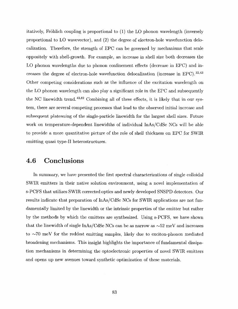
itatively, Fr6hlich coupling is proportional to (1) the LO phonon wavelength (inversely
proportional to LO wavevector), and (2) the degree of electron-hole wavefunction delo-
calization. Therefore, the strength of EPC can be governed by mechanisms that scale
oppositely with shell-growth. For example, an increase in shell size both decreases the
LO phonon wavelengths due to phonon confinement effects (decrease in EPC) and in-
creases the degree of electron-hole wavefunction delocalization (increase in EPC).12,
Other competing considerations such as the influence of the excitation wavelength on
the LO phonon wavelength can also play a significant role in the EPC and subsequently
the NC linewidth trend.43 82 Combining all of these effects, it is likely that in our sys-
tem, there are several competing processes that lead to the observed initial increase and
subsequent plateauing of the single-particle linewidth for the largest shell sizes. Future
work on temperature-dependent linewidths of individual InAs/CdSe NCs will be able
to provide a more quantitative picture of the role of shell thickness on EPC for SWIR
emitting quasi type-II heterostructures.
4.6 Conclusions
In summary, we have presented the first spectral characterizations of single colloidal
SWIR emitters in their native solution environment, using a novel implementation of
s-PCFS that utilizes SWIR corrected optics and newly developed SNSPD detectors. Our
results indicate that preparation of InAs/CdSe NCs for SWIR applications are not fun-
damentally limited by the linewidth or the intrinsic properties of the emitter but rather
by the methods by which the emitters are synthesized. Using s-PCFS, we have shown
that the linewidth of single InAs/CdSe NCs can be as narrow as -52 meV and increases
to -70 meV for the reddest emitting samples, likely due to exciton-phonon mediated
broadening mechanisms. This insight highlights the importance of fundamental dissipa-
tion mechanisms in determining the optoelectronic properties of novel SWIR emitters
and opens up new avenues toward synthetic optimization of these materials.
83

84
.? ' -o:w .-. -...- - - - :' '. - - - : ,. - 1- 1 - 1 .. . - .. -. --..

Chapter 5
Future Directions
5.1 s-PCFS of Lead Sulfide Nanocrystals
While we are able to observe the single NC linewidths of NIR emissive PbS, it remains
an outstanding challenge to study larger PbS NCs emissive in the SWIR. Because the
PbS samples have comparable or better quantum yield than the InAs samples, this
inability to make this measurement is due to either sample degradation or the long
photoluminescence lifetime of the PbS emitters.
We employ a few different strategies with NCs to stabilize them at low concentrations
in solution. Typically in a single NC solution experiment we are working at nano molar
(nM) concentrations and the NCs are not always colloidally stable at such high dilutions.
With other systems, including CdSe, and InAs, we stabilize these emitters in solution by
adding extra ligand to the solution such that if we strip the surface by adding solvent,
we don't disturb the equilibrium between the ligands and the surface. The surface of the
PbS NCs are coated with oleic acid and if we add oleic acid into the solution, we observe
an etching of the surface accompanied by a blue shift in the emission of the NCs (as
shown in figure 5-1 (c) and inset). We have also shown that amine terminated molecules
can help stabilize NCs in solution because they bind more tightly to the surface of the
NC and don't strip off as easily. We see that the addition of Oleylamine as shown
in figure 5-1 (a) actually boosts the QY of the solution by 20% but upon addition of
too much oleylamine, we start to reduce the enhancement in the QY. It has also been
85

hypothesized that in PbS NCs the reason for the dilution instability stems from empty
lead surface sites so we attempt the addition of lead oleate to boost the PLQY and, in
fact, this seems to help (figure 5-1 (b)).
We have seen, and it has been reported that PbS has photoluminescence lifetime
is on the order of 1 - 10 ps. Typically when we perform an FCS measurement we see
that our emitters have remain in the focal volume on the order of a one millisecond.
Assuming that our emitter has 50% QY, this amounts to at most 500 photons emitted
while in the focal volume. Compare this to an emitter like InAs which has a lifetime
of 100 ns which would result in an order of magnitude more photons emitted while in
the focal volume. Practically speaking, the s-PCFS experiment with PbS is unfeasible
with our current technology. There are several upgrades that can be made in order to
achieve this measurement. On the sample side we will need to first solve the stability
problems, perhaps through ligand engineering. On the hardware side we will need to
optimize the optical system as much as possible. This has become possible recently with
the advances in the SNSPDs. There are now commercial SNSPD systems where each
detector has 90% efficiency. This will boost our signal by a factor of 3, and if we have
access to all of the four channels on each detector, this will give us another factor of 2
in signal. Beyond this, we await more transmissive focusing objectives.
One other alternative is to engineer the focal volume so as to minimize it. As it
stands, we are diffraction-limited in our focal volume, but if we transition to a total
internal reflection fluorescence (TIRF) microscope geometry where we can decrease the
effective focal volume below the diffraction limit. This way we could keep the solu-
tion more concentrated and enhance stability while still only interrogating a very small
volume. Of course this comes with its own set of challenges because TIRF objectives
are extremely difficult to chromatically correct due to the oblique angle from which the
sample is excited.
5.1.1 Preliminary SWIR PbS s-PCFS Results
The s-PCFS data taken in figure 5-2 (b) was the only successful data set that we
have obtained and, even with that, the SNR could be improved. This sample was a
86
1.2
1
(a)
-'
C:
N
.E
0Z)
1000 1200Wavelength
1.2
1
0.8 -
0.6
0.4
0.2
0900
I I
--Pure+OA
- -- +A+Oly-+PbOleate
1400
(nm)
(b)1.2--- Pure
-+1X Oly-- +2X Oly.-- +5X Oly
1
0.8 -
0.6 -
0.4 -
0.21-
01000 1200 1400Wavelength (nm)
0
Cnr-
I
1
%W e 1100 1150h
Wavelength
1000 1100 1200Wavelength
1300(nm)
1400
1200
(nm)-
1500
Figure 5-1: This figure summarizes the different strategies used to boost PLQY andstabilize nanocrystals at single-nanocrystal spectroscopy concentrations. (a) Differentconcentrations of Oleylamine can be added to the solution of nanocrystals and thisboosts the PLQY of the overall solution. Too much Oleylamine does eventually degradethe NCs. (b) Oleate with cation attached can be used to fill in the surface of the NCand boost PLQY at high dilutions. (c) Adding excess Oleic Acid can help to stabilizeNCs in solution by pushing equilibrium such that the surface of the NC does not loseligands. When too much acid is added, it starts to etch the surface of the NC and theemission starts to blueshift (inset).
PbS sample emissive at 1500 nm that was provided by QD Vision. The details of the
synthesis and the surface characteristics are not known but the sample was stable enough
87
Z
- -- Pure-- +PbAcetate
0.8
0.6
0.4
0.2
01
Cl)C
CE
0z
. . .
M

(a) x103 (b)14 .. -Ensemble.
12 - 159 meV
S 0.8 -single:
.0 152 meV
c- -o.6aI)
4 NO.40 2 C
E 0.2.0 ------------2 _Z 0
104 10-2 100 -300-200 -100 0 100 200 300Lag Time (s) Spectral Correlation (meV)
Figure 5-2: This figure summarizes the results of an s-PCFS experiment on a solution ofPbS NCs emissive at 1500nm. (a) This panel is a representative fluorescence correlationtrace during this experiment. We can see that there is an average focal occupation of-85 NCs. (b) This panel summarized the spectral correlations of the ensemble of NCsand the single NCs. We see that the spectral correlation of the ensemble of emitters is159 meV and the single emitters is 152 meV.
to survive a 20 hour experiment. We can tell from the FCS trace (figure 5-2 (a)) that
the occupation of the focal volume was -85 particles. This occupation volume is not
significantly different from what we have seen with other PbS samples, suggesting that
the sample has been significantly stabilized. From this data, however, we can see that
just as with the NIR emissive PbS NCs, the SWIR emissive PbS NCs exhibit broad single
nanocrystal linewidths. These single NC linewidths match the ensemble linewidths,
suggesting that homogeneous broadening is the dominant broadening in these systems.
In order to disentangle the emission mechanisms in these materials, we will need to do
some low temperature single NC spectroscopy.
5.2 Temperature-Dependent Spectroscopy of Single
InAs QDs
From our results in Chapter 4 we found that the ensemble linewidth of InAs/CdSe
NCs was dominated by inhomogeneous broadening effects. By deconvoluting the effects
of sample heterogeneity, we found that the single NC linewidth is comparable to some
of the narrowest emitters in the visible, including CdSe and InP. We have separated out
88

inhomogeneous broadening effects and further experiments on InAs NCs should focus
on understanding the physical mechanisms that underlie InAs emission and contribute
to the homogeneous linewidth.
We rarely observe NC systems that exhibit lifetime-limited emission linewidths. Most
systems undergo excess broadening due to spectral fluctuations13 ,, coupling to phonon
modes' 3 , and the presence of excitonic fine structure.31 47 0 5"06' 126 Ideally we would
like too assemble a complete picture of the emission mechanisms in these NC systems and
understand the underlying synthetic tools to alter specific characteristics. In order to
understand the physical mechanisms, we must take these systems to low temperature and
study the differences in their emissive properties. Through low temperature experiments
we can get at the fluorescence linewidths, lifetimes of different emissive states, and
coherence properties.
bright
AE dark
kbright kdark
ground
Figure 5-3: This is a cartoon of the energy diagram of the excitonic fine structure inInAs NCs. There is a dark state and a bright state separated by some energy AE andeach of these states have decay rates back to the ground state (kbright and kdark).
We studied the ensemble photoluminescence lifetimes in InAs/CdSe NCs and found
them to be multiexponential suggesting that several different radiative and non-radiative
processes occurr in the NCs. What we found and what others have found is that the
bright state lifetime in these NCs is on the order of -r =- 150ns. 1 2 ,16 Others have
taken these measurements down to low temperature and found that the lifetime actually
lengthens to r =- 2ps. 15 This behavior suggests the presence of excitonic fine structure
89

(a) (b)7000C10
: 20 6000 265000 o
40000
3000 $ 280 S20000-28
1000 D,150 154 Counts 154 156
Position (Microns) Position (Microns)(c)
u)300-
0
a.80_Jj
0 5 10 15 20 25 30 35 40
Time (Seconds)
Figure 5-4: (a) Using a piezoelectric stage we scan a film of spin-cast InAs/CdSe/ZnSNCs and we zoom in on the red box. This shows that our emitters are well dispersedand isolated on our film. (b) This is a finer scan of the area in the red box in panel(a) in which we can see "stripes" due to the fluorescence intermittency of the emitter aswe scan the piezo. (c) This panel shows a fluorescence intermittency trace for a singleInAs/CdSe/ZnS QD (Dot 1) at room temperature. This work, along with work fromothers, paves the way for single NC spectra of InAs NCs. This particular NC showswell-behaved two-state blinking.
as outlined in figure 5-3 where there is a bright state that recombines with rate of kbright
and a dark state that lies lower in energy that recombines with rate of kdark. In this
picture emission from the dark state is spin-forbidden and that from the bright state is
spin-allowed. In many NC systems, including this one, the dark state lies lower in energy
than the bright state and we can recover the energy difference between the two states
by varying the temperature of the system to determine at what point we are thermally
populating only the dark state. Others have done ensemble measurements of the low
temperature lifetimes and have found that in this system, the splitting (AE) is on the
order of 2 meV. " This is similar to what has been seen in other NC systems including
90

CdSe.113
While our data suggests that there is a lowest lying dark state in InAs, these fluo-
rescence lifetimes do not accurately capture the dynamics at play because it is based on
an ensemble measurement and thus there are a distribution of splitting energies present.
In order to study this, we would need to do low temperature single NC lifetimes of InAs
NCs.
Our group has been able to isolate single InAs NCs on a substrate and study their
fluorescence lifetimes. 16 We were able to replicate this data, as shown in figure 5-4, where
we see two-state blinking behavior from a single InAs NC.
5.3 Conclusions
Colloidal nanocrystals are promising materials for applications requiring high-throughput
synthesis and solution-compatible deposition. The success of these materials in commer-
cial products will depend directly on the mastery of our synthetic techniques and the
knowledge about the physical processes that govern absorption and emission events.
Visible-emissive colloidal nanocrystals have been well explored because of the wealth of
detectors sensitive to visible light. As infrared detector technology continues to become
declassified, we can begin to explore more and more applications of infrared emitters
(even ones that we haven't thought of yet!). As with visible emitters, we need to have
an understanding and a mastery of the synthesis and physical properties of these materi-
als before we can begin to commercialize them. We are still far from commercialization
of infrared emissive materials due to: unoptimized syntheses, and toxicity concerns.
Hopefully this work provides a platform for more research into infrared emissive mate-
rials.
91

92
.I .# ..... ,..1 ,i -i il nilne'l -a

Appendix A
Spectral Transmission of Microscope
Objectives
A.1 Zeiss EC Epiplan-Neofluar 100X/0.9 NA
Many of our single NC experiments require low temperature and as such, we typically
excite our film of single NCs through an optical window with a long working distance
objective. Optical windows on most cryostats are typically tens of millimeters thick.
These long working distance objectives are all air immersion objectives typically with
numerical apertures limited to <0.5. Because of these low NAs, the collection efficiency
of these objectives suffers. In response, Montana Instruments built a Cryo-Optic attach-
ment that allows the microscope objective to be housed inside of the vacuum chamber
and thus can be as close to the sample as needed. We have one such attachment and
because we planned to work with SWIR emitters in the cryostat, we needed a microscope
objective that was both vacuum compatible, air immersion, and transmissive through
the SWIR. Zeiss is one of the only companies that makes vacuum-compatible objectives.
This is because the epoxies used to fasten the lenses together must be vacuum epoxies
and must not out-gas when vacuum is applied. Zeiss in collaboration with Montana
Instruments built a series of vacuum compatible microscope objectives with NA of 0.75,
0.85 or 0.9 depending on what collection volume you need. We have the 0.9 NA objective
and although there is only information about the transmission of this objective out to
93

1100 nm on the Montana Instruments website, we have tested the transmission of this
objective across the SWIR using a broadband lamp and an IR spectrometer. Figure
A-1 shows the transmission of this objective lens across the visible (data from Montana
Instruments) and the SWIR (our data).
100-m From Montana Instruments Website
90 - SWIR Transmission Data from MIT
80
C 700Cnn60E
C: 50
40
30
20
10
0200 400 600 800 1000 1200 1400 1600 1800 2000 2200
Wavelength (nm)
Figure A-1: This is the expanded transmission curve for the Zeiss EC Epiplan-Neofluar100X/0.90 NA objective. The data shown in blue is from the Montana Instrumentswebsite specs for this objective and the data in green was taken using a broadband lampwith uniform emission across the SWIR. The transmission spectrum was recorded usingan Ocean Optics IR Spectrometer and stitched together with the Montana InstrumentsData
A.2 CFI Nikon Plan Apo IR 60X/1.27 NA WI
The microscope objective used in all of the s-PCFS experiments throughout this
thesis is the CFI Nikon Plan Apo IR objective. We have taken a transmission spectrum
throughout the SWIR as shown in Figure A-2. While the specific transmission curve
through the visible of this objective is proprietary, we do know that the transmission at
94

530 nm (the wavelength of our excitation source) is 89%.
100
90
80
700- 60
i50CU
40
30
20
10
0 "800 1000 1200 1400 1600 1800 2000 2200
Wavelength (nm)
Figure A-2: This is the expanded transmission curve for the CFI Nikon Plan Apo IR
60X WI Objective. The data was taken using a broadband lamp with uniform emission
across the SWIR. The transmission spectrum was recorded using an Ocean Optics IR
Spectrometer.
95

96

Bibliography
[1] N. M. Abdelazim, Q. Zhu, Y. Xiong, Y. Zhu, M. Chen, N. Zhao, S. V. Ker-shaw, and A. L. Rogach. Room Temperature Synthesis of HgTe Quantum Dotsin an Aprotic Solvent Realizing High Photoluminescence Quantum Yields in theInfrared. Chemistry of Materials, 29(18):7859-7867, Sept. 2017. ISSN 0897-4756,1520-5002. doi: 10.1021/acs.chemmater.7b02637.
[2] S. Aghaeimeibodi, C.-M. Lee, M. A. Buyukkaya, C. J. K. Richardson, and E. Waks.Large stark tuning of InAs/InP quantum dots. Applied Physics Letters, 114(7):071105, Feb. 2019. ISSN 0003-6951, 1077-3118. doi: 10.1063/1.5082560.
[3] A. Aharoni, T. Mokari, I. Popov, and U. Banin. Synthesis of InAs/CdSe/ZnSecore/shelll/shell2 structures with bright and stable near-infrared fluorescence.128(1):257-264. ISSN 0002-7863, 1520-5126. doi: 10.1021/ja056326v. URLhttp://pubs.acs. org/doi/abs/10. 1021/ja056326v.
[4] I. Aharonovich, D. Englund, and M. Toth. Solid-state single-photon emitters.Nature Photonics, 10(10):631-641, Oct. 2016. ISSN 1749-4885, 1749-4893. doi:10. 1038/nphoton.2016.186.
[5] P. M. Allen and M. G. Bawendi. Ternary 1-III-VI Quantum Dots Luminescentin the Red to Near-Infrared. J. Am. Chem. Soc., 130(29):9240-9241, July 2008.ISSN 0002-7863. doi: 10.1021/ja8036349.
[6] P. M. Allen, W. Liu, V. P. Chauhan, J. Lee, A. Y. Ting, D. Fukumura, R. K.Jain, and M. G. Bawendi. InAs(ZnCdS) quantum dots optimized for biologicalimaging in the near-infrared. 132(2):470-471. ISSN 0002-7863, 1520-5126. doi:10.1021/ja908250r. URL http://pubs. acs. org/doi/abs/10. 1021/ja908250r.
[7] W. P. Ambrose, T. Basch, and W. E. Moerner. Detection and spectroscopy ofsingle pentacene molecules in a p terphenyl crystal by means of fluorescence ex-citation. 95(10):7150-7163. ISSN 0021-9606, 1089-7690. doi: 10.1063/1.461392.URL http://aip.scitation.org/doi/10.1063/1.461392.
[8] A. L. Antaris, H. Chen, K. Cheng, Y. Sun, G. Hong, C. Qu, S. Diao,Z. Deng, X. Hu, B. Zhang, X. Zhang, 0. K. Yaghi, Z. R. Alamparambil,X. Hong, Z. Cheng, and H. Dai. A small-molecule dye for NIR-I imaging.15(2):235-242. ISSN 1476-1122, 1476-4660. doi: 10.1038/nmat4476. URLhttp: //www. nature. com/articles/nmat4476.
97

[9] C. R. Baiz, D. Schach, and A. Tokmakoff. Ultrafast 2d IR microscopy.22(15):18724. ISSN 1094-4087. doi: 10.1364/OE.22.018724. URLhttps: //www. osapublishing. org/oe/abstract. cfm?uri=oe-22-15-18724.
[10] P. Barcik, 0. Wilfert, and Z. Kolka. Diffraction of the opti-cal wave in the schmidt cassegrain telescope. pages 1-5. IEEE.ISBN 978-1-5090-4594-5. doi: 10.1109/COMITE.2017.7932303. URLhttp://ieeexplore.ieee.org/document/7932303/.
[11] F. Bellei, A. P. Cartwright, A. N. McCaughan, A. E. Dane, F. Najafi, Q. Zhao,and K. K. Berggren. Free-space-coupled superconducting nanowire single-photondetectors for infrared optical communications. Optics Express, 24(4):3248, Feb.2016. ISSN 1094-4087. doi: 10.1364/OE.24.003248.
[12] S. N. Bertram, B. Spokoyny, D. Franke, J. R. Caram, J. J. Yoo, R. P. Murphy,M. E. Grein, and M. G. Bawendi. Single Nanocrystal Spectroscopy of ShortwaveInfrared Emitters. ACS Nano, Nov. 2018. ISSN 1936-0851, 1936-086X. doi:10.1021/acsnano.8b07578.
[13] A. P. Beyler, L. F. Marshall, J. Cui, X. Brokmann, and M. G. Bawendi. DirectObservation of Rapid Discrete Spectral Dynamics in Single Colloidal CdSe-CdSCore-Shell Quantum Dots. Physical Review Letters, 111(17), Oct. 2013. ISSN0031-9007, 1079-7114. doi: 10.1103/PhysRevLett.111.177401.
[14] M. D. Birowosuto, H. Sumikura, S. Matsuo, H. Taniyama, P. J. van Veldhoven,R. N6tzel, and M. Notomi. Fast Purcell-enhanced single photon source in 1,550-nmtelecom band from a resonant quantum dot-cavity coupling. Scientific Reports, 2,Dec. 2012.
[15] T. S. Bischof. On the Origin of Photons: Understanding Excitons and Multiexci-tons in Colloidal Semiconductor Nanocrystals. PhD thesis.
[16] T. S. Bischof, R. E. Correa, D. Rosenberg, E. A. Dauler, and M. G.Bawendi. Measurement of emission lifetime dynamics and biexciton emis-sion quantum yield of individual InAs colloidal nanocrystals. 14(12):6787-6791. ISSN 1530-6984, 1530-6992. doi: 10.1021/n502180w. URLhttp://pubs.acs.org/doi/10.1021/n1502180w.
[17] D. M. Boroson, B. S. Robinson, D. V. Murphy, D. A. Burianek, F. Khatri, J. M.Kovalik, Z. Sodnik, and D. M. Cornwell. Overview and results of the Lunar LaserCommunication Demonstration. In H. Hemmati and D. M. Boroson, editors, SPIELASE, page 89710S, San Francisco, California, United States, Mar. 2014. doi:10.1117/12.2045508.
[18] X. Brokmann, L. F. Marshall, and M. G. Bawendi. Revealing single emitter spec-tral dynamics from intensity correlations in an ensemble fluorescence spectrum.Opt. Express, 17(6):4509-4517, 2009. doi: 10. 1364/OE. 17.004509.
98

[19] 0. T. Bruns, T. S. Bischof, D. K. Harris, D. Franke, Y. Shi, L. Riedemann,A. Bartelt, F. B. Jaworski, J. A. Carr, C. J. Rowlands, M. W. Wilson, 0. Chen,H. Wei, G. W. Hwang, D. M. Montana, I. Coropceanu, 0. B. Achorn, J. Kloep-per, J. Heeren, P. T. So, D. Fukumura, K. F. Jensen, R. K. Jain, and M. G.Bawendi. Next-generation in vivo optical imaging with short-wave infraredquantum dots. 1. ISSN 2157-846X. doi: 10.1038/s41551-017-0056. URLhttps://www.ncbi.nlm.nih.gov/pmc/articles/PMC5673283/.
[20] H. Buening Pfaue. Analysis of water in food by near infrared spectroscopy. FoodChemistry, 82(1):107-115, July, 2003.
[21] B. K. Byrd, M. R. Folaron, J. P. Leonor, R. R. Strawbridge, X. Cao, P. Bruza, andS. C. Davis. Characterizing short-wave infrared fluorescence of conventional near-infrared fluorophores. Journal of Biomedical Optics, 24(03):1, Mar. 2019. ISSN1083-3668. doi: 10.1117/1.JBO.24.3.035004.
[22] M. P. Campos, M. P. Hendricks, A. N. Beecher, W. Walravens, R. A. Swain,G. T. Cleveland, Z. Hens, M. Y. Sfeir, and J. S. Owen. A Library of SelenoureaPrecursors to PbSe Nanocrystals with Size Distributions near the HomogeneousLimit. Journal of the American Chemical Society, 139(6):2296-2305, Feb. 2017.ISSN 0002-7863, 1520-5126. doi: 10.1021/jacs.6b11021.
[23] J. R. Caram, S. N. Bertram, H. Utzat, W. R. Hess, J. A. Carr, T. S. Bischof,A. P. Beyler, M. W. B. Wilson, and M. G. Bawendi. PbS Nanocrystal EmissionIs Governed by Multiple Emissive States. Nano Letters, 16(10):6070-6077, Oct.2016. ISSN 1530-6984. doi: 10.1021/acs.nanolett.6b02147.
[24] J. A. Carr, D. Franke, J. R. Caram, C. F. Perkinson, M. Saif,V. Askoxylakis, M. Datta, D. Fukumura, R. K. Jain, M. G. Bawendi,and 0. T. Bruns. Shortwave infrared fluorescence imaging with theclinically approved near-infrared dye indocyanine green. page 201718917.ISSN 0027-8424, 1091-6490. doi: 10.1073/pnas.1718917115. URLhttp://www.pnas.org/content/early/2018/04/05/1718917115.
[25] G. Cerullo, S. De Silvestri, and U. Banin. Size-dependent dynamics of coherentacoustic phonons in nanocrystal quantum dots. Physical Review B, 60(3):1928-1932, July 1999. ISSN 0163-1829, 1095-3795. doi: 10.1103/PhysRevB.60.1928.
[26] Y. Chen, D. M. Montana, H. Wei, J. M. Cordero, M. Schneider, X. Le Guevel,0. Chen, 0. T. Bruns, and M. G. Bawendi. Shortwave Infrared in Vivo Imagingwith Gold Nanoclusters. Nano Letters, 17(10):6330-6334, Oct. 2017. ISSN 1530-6984, 1530-6992. doi: 10.1021/acs.nanolett.7b03070.
[27] R. E. Correa, E. A. Dauler, G. Nair, S. H. Pan, D. Rosenberg, A. J. Ker-man, R. J. Molnar, X. Hu, F. Marsili, V. Anant, K. K. Berggren, and M. G.Bawendi. Single photon counting from individual nanocrystals in the infrared.12(6):2953-2958. ISSN 1530-6984, 1530-6992. doi: 10.1021/n1300642k. URLhttp://pubs.acs.org/doi/10. 1021/n1300642k.
99

[28] E. D. Cosco, J. R. Caram, 0. T. Bruns, D. Franke, R. A. Day, E. P. Farr, M. G.Bawendi, and E. M. Sletten. Flavylium Polymethine Fluorophores for Near- andShortwave Infrared Imaging. Angewandte Chemie International Edition, 56(42):13126-13129, Oct. 2017. ISSN 14337851. doi: 10.1002/anie.201706974.
[29] I. J. Cox and C. J. R. Sheppard. Information capacity and resolution in an opticalsystem. 3(8):1152. ISSN 1084-7529, 1520-8532. doi: 10.1364/JOSAA.3.001152.URL https://www.osapublishing.org/abstract . cfm?URI=josaa-3-8-1152.
[30] J. Cui. Deconstructing the Room-Temperature Emisssion Spectra of NanocrystalsUsing Photon-Correlation Fourier Spectroscopy, 2014.
[31] J. Cui, A. P. Beyler, I. Coropceanu, L. Cleary, T. R. Avila, Y. Chen, J. M.Cordero, S. L. Heathcote, D. K. Harris, 0. Chen, J. Cao, and M. G. Bawendi.Evolution of the single-nanocrystal photoluminescence linewidth with size andshell: Implications for excitonphonon coupling and the optimization of spectrallinewidths. 16(1):289-296, . ISSN 1530-6984. doi: 10.1021/acs.nanolett.5b03790.URL https: //doi.org/10. 1021/acs.nanolett .5b03790.
[32] J. Cui, A. P. Beyler, L. F. Marshall, 0. Chen, D. K. Harris, D. D. Wanger,X. Brokmann, and M. G. Bawendi. Direct probe of spectral inhomogeneity revealssynthetic tunability of single-nanocrystal spectral linewidths. 5(7):602-606, . ISSN17554330. doi: 10.1038/nchem.1654.
[33] J. Cui, A. P. Beyler, L. F. Marshall, 0. Chen, D. K. Harris, D. D. Wanger,X. Brokmann, and M. G. Bawendi. Direct probe of spectral inhomogeneity revealssynthetic tunability of single-nanocrystal spectral linewidths. Nat. Chem., 5(7):602-606, 2013. doi: 10.1038/nchem.1654.
[34] J. Cui, A. P. Beyler, I. Coropceanu, L. Cleary, T. R. Avila, Y. Chen, J. M.Cordero, S. L. Heathcote, D. K. Harris, 0. Chen, J. Cao, and M. G. Bawendi.Evolution of the Single-Nanocrystal Photoluminescence Linewidth with Size andShell: Implications for Exciton-Phonon Coupling and the Optimization of Spec-tral Linewidths. Nano Lett., 16(1):289-296, Jan. 2016. ISSN 1530-6984. doi:10. 1021/acs.nanolett.5b03790.
[35] E. A. Dauler, M. E. Grein, A. J. Kerman, F. Marsili, S. Miki, S. W. Nam, M. D.Shaw, H. Terai, V. B. Verma, and T. Yamashita. Review of superconductingnanowire single-photon detector system design options and demonstrated perfor-mance. 53(8):081907, . ISSN 0091-3286. doi: 10.1117/1.OE.53.8.081907.
[36] E. A. Dauler, A. J. Kerman, B. S. Robinson, J. K. Yang, B. Voronov, G. Goltsman,S. A. Hamilton, and K. K. Berggren. Photon-number-resolution with sub-30-pstiming using multi-element superconducting nanowire single photon detectors. 56(2):364-373, . ISSN 0950-0340, 1362-3044. doi: 10.1080/09500340802411989. URLhttp://www.tandfonline. com/doi/abs/10. 1080/09500340802411989.
100

[37] B. De Geyter, A. J. Houtepen, S. Carrillo, P. Geiregat, Y. Gao, S. ten Cate, J. M.Schins, D. Van Thourhout, C. Delerue, L. D. A. Siebbeles, and Z. Hens. Broadbandand Picosecond Intraband Absorption in Lead-Based Colloidal Quantum Dots.ACS Nano, 6(7):6067-6074, July 2012. ISSN 1936-0851. doi: 10.1021/nn301149x.
[38] R. de Lamaestre, H. Bernas, D. Pacifici, G. Franz6, and F. Priolo. Evidence for a"dark exciton" state of PbS nanocrystals in a silicate glass. Appl. Phys. Lett., 88(18):181115-181116, 2006. doi: http://dx.doi.org/10.1063/1.2201885.
[39] E. L. Dereniak and T. D. Dereniak. Geometrical and Trigonometric Optics. Cam-bridge University Press, 2008. doi: 10.1017/CB09780511755637.
[40] S. Diao, J. L. Blackburn, G. Hong, A. L. Antaris, J. Chang, J. Z. Wu, B. Zhang,K. Cheng, C. J. Kuo, and H. Dai. Fluorescence imaging in vivo at wavelengths be-yond 1500 nm. 54(49):14758-14762. ISSN 14337851. doi: 10.1002/anie.201507473.URL http://doi.wiley.com/10.1002/anie.201507473.
[41] X. Ding, Y. He, Z.-C. Duan, N. Gregersen, M.-C. Chen, S. Unsleber, S. Maier,C. Schneider, M. Kamp, S. H6fling, C.-Y. Lu, and J.-W. Pan. On-Demand Sin-gle Photons with High Extraction Efficiency and Near-Unity Indistinguishabilityfrom a Resonantly Driven Quantum Dot in a Micropillar. Physical Review Let-ters, 116(2):020401, Jan. 2016. ISSN 0031-9007, 1079-7114. doi: 10.1103/Phys-RevLett.116.020401.
[42] B. Dong, C. Li, G. Chen, Y. Zhang, Y. Zhang, M. Deng, and Q. Wang. FacileSynthesis of Highly Photoluminescent Ag 2 Se Quantum Dots as a New Fluo-rescent Probe in the Second Near-Infrared Window for in Vivo Imaging. Chem-istry of Materials, 25(12):2503-2509, June 2013. ISSN 0897-4756, 1520-5002. doi:10.1021/cm400812v.
[43] V. M. Dzhagan, M. Ya Valakh, A. E. Raevskaya, A. L. Stroyuk, S. Y. Kuchmiy,and D. R. T. Zahn. Size effects on raman spectra of small CdSe nanoparticlesin polymer films. 19(30):305707. ISSN 0957-4484, 1361-6528. doi: 10.1088/0957-4484/19/30/305707.
[44] M. D. Eisaman, J. Fan, A. Migdall, and S. V. Polyakov. Invited Review Arti-cle: Single-photon sources and detectors. Review of Scientific Instruments, 82(7):071101, July 2011. ISSN 0034-6748, 1089-7623. doi: 10.1063/1.3610677.
[45] R. J. Ellingson, M. C. Beard, J. C. Johnson, P. Yu, 0. I. Micic, A. J. Nozik,A. Shabaev, and A. L. Efros. Highly Efficient Multiple Exciton Generation inColloidal PbSe and PbS Quantum Dots. Nano Letters, 5(5):865-871, May 2005.ISSN 1530-6984, 1530-6992. doi: 10.1021/n0502672.
[46] M. J. Fernee, P. Jensen, and H. Rubinsztein-Dunlop. Origin of the Large Homo-geneous Line Widths Obtained from Strongly Quantum Confined PbS Nanocrys-tals at Room Temperature. J. Phys. Chem. C, 111(13):4984-4989, 2007. doi:10.1021/jp067523z.
101
[47] M. J. Fern6e, C. Sinito, Y. Louyer, P. Tamarat, and B. Lounis. The ultimate limitto the emission linewidth of single nanocrystals. Nanotechnology, 24(46):465703,Nov. 2013. ISSN 0957-4484, 1361-6528. doi: 10.1088/0957-4484/24/46/465703.
[48] D. Franke. Fluorescent Materials for Short- Wave Infrared Imaging. PhD thesis.
[49] D. Franke, D. K. Harris, 0. Chen, 0. T. Bruns, J. A. Carr, M. W. B.Wilson, and M. G. Bawendi. Continuous injection synthesis of in-dium arsenide quantum dots emissive in the short-wavelength in-frared. 7:12749. ISSN 2041-1723. doi: 10. 1038/ncommsl2749. URLhttps: //www . nature. com/articles/ncomms12749.
[50] H. Fr6hlich. Electrons in lattice fields. Adv. Phys., 3(11):325-361, July 1954. ISSN0001-8732. doi: 10.1080/00018735400101213.
[51] J. Gao and J. C. Johnson. Charge Trapping in Bright and Dark States of CoupledPbS Quantum Dot Films. A CS Nano, 6(4):3292-3303, Apr. 2012. ISSN 1936-0851.doi: 10.1021/nn300707d.
[52] M. S. Gaponenko, A. A. Lutich, N. A. Tolstik, A. A. Onushchenko, A. M. Mal-yarevich, E. P. Petrov, and K. V. Yumashev. Temperature-dependent photolumi-nescence of PbS quantum dots in glass: Evidence of exciton state splitting andcarrier trapping. Phys. Rev. B, 82(12):125320, Sept. 2010. doi: 10.1103/Phys-RevB.82.125320.
[53] D. Ghosh, A. F. Bagley, Y. J. Na, M. J. Birrer, S. N. Bhatia, and A. M. Belcher.Deep, noninvasive imaging and surgical guidance of submillimeter tumors usingtargeted M13-stabilized single-walled carbon nanotubes. Proceedings of the Na-tional Academy of Sciences, 111(38):13948-13953, Sept. 2014. ISSN 0027-8424,1091-6490. doi: 10.1073/pnas.1400821111.
[54] G. N. Goltsman, 0. Okunev, G. Chulkova, A. Lipatov, A. Semenov,K. Smirnov, B. Voronov, A. Dzardanov, C. Williams, and R. Sobolewski.Picosecond superconducting single-photon optical detector. 79(6):705-707. ISSN 0003-6951, 1077-3118. doi: 10.1063/1.1388868. URLhttp://aip.scitation.org/doi/10.1063/1.1388868.
[55] M. H. Greenblatt. On the measurement of transit time dispersion in multiplierphototubes. 5(1):13-16. ISSN 0096-2015. doi: 10.1109/TNS2.1958.4315600. URLhttp://ieeexplore.ieee. org/document/4315600/.
[56] D. Grodziniska, W. H. Evers, R. Dorland, J. van Rijssel, M. A. van Huis, A. Mei-jerink, C. de Mello Donega, and D. Vanmaekelbergh. Two-Fold Emission From theS-Shell of PbSe/CdSe Core/Shell Quantum Dots. Small, 7(24):3493-3501, 2011.ISSN 1613-6829. doi: 10.1002/smll.201101819.
[57] Y.-P. Gu, R. Cui, Z.-L. Zhang, Z.-X. Xie, and D.-W. Pang. Ultrasmall Near-Infrared Ag 2 Se Quantum Dots with Tunable Fluorescence for in Vivo Imaging.
102

Journal of the American Chemical Society, 134(1):79-82, Jan. 2012. ISSN 0002-7863, 1520-5126. doi: 10.1021/ja2089553.
[58] E. H. Sargent. Infrared Quantum Dots. Advanced Materials, 17(5):515-522, Mar.2005. ISSN 0935-9648, 1521-4095. doi: 10.1002/adma.200401552.
[59] T. Ha, A. Y. Ting, J. Liang, W. B. Caldwell, A. A. Deniz, D. S.Chemla, P. G. Schultz, and S. Weiss. Single-molecule fluorescence spec-troscopy of enzyme conformational dynamics and cleavage mechanism. 96(3):893-898. ISSN 0027-8424, 1091-6490. doi: 10.1073/pnas.96.3.893. URLhttp://www.pnas.org/cgi/doi/10.1073/pnas.96.3.893.
[60] R. H. Hadfield. Single-photon detectors for optical quantum information applica-tions. Nature Photonics, 3(12):696-705, Dec. 2009. ISSN 1749-4885, 1749-4893.doi: 10.1038/nphoton.2009.230.
[61] D. K. Harris, P. M. Allen, H.-S. Han, B. J. Walker, J. Lee, and M. G. Bawendi. Syn-thesis of Cadmium Arsenide Quantum Dots Luminescent in the Infrared. Journalof the American Chemical Society, 133(13):4676-4679, Apr. 2011. ISSN 0002-7863,1520-5126. doi: 10.1021/ja1101932.
[62] J. E. Harvey and C. Ftaclas. Diffraction effects of telescope sec-ondary mirror spiders on various image-quality criteria. 34(28):6337. ISSN 0003-6935, 1539-4522. doi: 10.1364/AO.34.006337. URLhttps://www.osapublishing.org/abstract.cfm?URI=ao-34-28-6337.
[63] S. Hatami, C. Wirth, M. Kaiser, S. Leubner, S. Gabriel, L. Bahrig, V. Lesnyak,J. Pauli, N. Gaponik, A. Eychmiiller, and U. Resch-Genger. Absolute photolumi-nescence quantum yields of IR26 and IR-emissive Cd 1-x Hg , Te and PbS quantumdots - method- and material-inherent challenges. Nanoscale, 7(1):133-143, 2015.ISSN 2040-3364, 2040-3372. doi: 10.1039/C4NR04608K.
[64] C. Hazra, S. Ullah, Y. E. Serge Correales, L. G. Caetano, and S. J. L. Ribeiro.Enhanced NIR-I emission from water-dispersible NIR-II dye-sensitized core/activeshell upconverting nanoparticles. Journal of Materials Chemistry C, 6(17):4777-4785, 2018. ISSN 2050-7526, 2050-7534. doi: 10.1039/C8TC00335A.
[65] M. P. Hendricks, M. P. Campos, G. T. Cleveland, I. Jen-La Plante, and J. S. Owen.A tunable library of substituted thiourea precursors to metal sulfide nanocrys-tals. Science, 348(6240):1226-1230, 2015. ISSN 0036-8075. doi: 10.1126/sci-ence.aaa2951.
[66] M. A. Hines and G. D. Scholes. Colloidal PbS Nanocrystals with Size-TunableNear-Infrared Emission: Observation of Post-Synthesis Self-Narrowing of the Par-ticle Size Distribution. Adv. Mater., 15(21):1844-1849, 2003. ISSN 1521-4095. doi:10.1002/adma.200305395.
103

[67] G. Hong, J. C. Lee, J. T. Robinson, U. Raaz, L. Xie, N. F. Huang,J. P. Cooke, and H. Dai. Multifunctional in vivo vascular imaging usingnear-infrared II fluorescence. 18(12):1841, . doi: 10.1038/nm.2995. URLhttps://www.ncbi.nlm.nih.gov/pmc/articles/PMC3595196/.
[68] G. Hong, Y. Zou, A. L. Antaris, S. Diao, D. Wu, K. Cheng, X. Zhang, C. Chen,B. Liu, Y. He, J. Z. Wu, J. Yuan, B. Zhang, Z. Tao, C. Fukunaga, and H. Dai.Ultrafast fluorescence imaging in vivo with conjugated polymer fluorophores in thesecond near-infrared window. 5(1), . ISSN 2041-1723. doi: 10.1038/ncomms5206.URL http://www. nature .com/articles/ncomms5206.
[69] G. W. Hwang, D. Kim, J. M. Cordero, M. W. B. Wilson, C.-H. M. Chuang, J. C.Grossman, and M. G. Bawendi. Identifying and Eliminating Emissive Sub-bandgapStates in Thin Films of PbS Nanocrystals. Adv. Mater., 27(30):4481-4486, 2015.ISSN 1521-4095. doi: 10.1002/adma.201501156.
[70] K. S. Ilin, I. I. Milostnaya, A. A. Verevkin, G. N. Goltsman, E. M. Gershenzon, andR. Sobolewski. Ultimate quantum efficiency of a superconducting hot-electron pho-todetector. 73(26):3938-3940. ISSN 0003-6951, 1077-3118. doi: 10.1063/1.122942.URL http://aip.scitation.org/doi/10.1063/1.122942.
[71] D. H. Jara, K. G. Stamplecoskie, and P. V. Kamat. Two Distinct Transitionsin CuxInS2 Quantum Dots. Bandgap versus Sub-Bandgap Excitations in Copper-Deficient Structures. J. Phys. Chem. Lett., 7(8):1452-1459, Apr. 2016. ISSN1948-7185. doi: 10.1021/acs.jpclett.6b00571.
[72] I. Kang and F. W. Wise. Electronic structure and optical properties of PbSand PbSe quantum dots. J. Opt. Soc. Am. B, 14(7):1632-1646, July 1997. doi:10. 1364/JOSAB. 14.001632.
[73] I. Kang and F. W. Wise. Electronic structure and optical properties of PbS andPbSe quantum dots. Journal of the Optical Society of America B, 14(7):1632, July1997. ISSN 0740-3224, 1520-8540. doi: 10.1364/JOSAB.14.001632.
[74] P. Kapusta, editor. Advanced Photon Counting: Applications, Methods, Instru-mentation. Number Vol. 15 in Springer Series on Fluorescence. Springer, Cham,2015. ISBN 978-3-319-15635-4 978-3-319-15636-1. OCLC: 912008024.
[75] A. J. Kerman, D. Rosenberg, R. J. Molnar, and E. A. Dauler. Readout of su-perconducting nanowire single-photon detectors at high count rates. Journal ofApplied Physics, 113(14):144511, Apr. 2013. ISSN 0021-8979, 1089-7550. doi:10.1063/1.4799397.
[76] S. Keuleyan, J. Kohler, and P. Guyot-Sionnest. Photoluminescence of Mid-InfraredHgTe Colloidal Quantum Dots. The Journal of Physical Chemistry C, 118(5):2749-2753, Feb. 2014. ISSN 1932-7447, 1932-7455. doi: 10.1021/jp409061g.
104
[77] S. Kim, B. Fisher, H.-J. Eisler, and M. Bawendi. Type-II quantum dots:CdTe/CdSe(core/shell) and CdSe/ZnTe(core/shell) heterostructures. 125(38):11466-11467. ISSN 0002-7863, 1520-5126. doi: 10.1021/ja0361749. URLhttp: //pubs. acs. org/doi/abs/10 . 1021/ja0361749.
[78] S. Kimura and T. Wilson. Confocal scanning optical micro-scope using single-mode fiber for signal detection. 30(16):2143.ISSN 0003-6935, 1539-4522. doi: 10. 1364/AO.30.002143. URLhttps://www.osapublishing.org/abstract.cfm?URI=ao-30-16-2143.
[79] M.-A. Langevin, A. M. Ritcey, and C. N. Allen. Air-Stable Near-Infrared AgInSe 2Nanocrystals. ACS Nano, 8(4):3476-3482, Apr. 2014. ISSN 1936-0851, 1936-086X.doi: 10.1021/nn406439w.
[80] J.-S. Lee, M. V. Kovalenko, J. Huang, D. S. Chung, and D. V. Talapin. Band-like transport, high electron mobility and high photoconductivity in all-inorganicnanocrystal arrays. Nat Nano, 6(6):348-352, June 2011. ISSN 1748-3387.
[81] Z. F. Li and E. Ruckenstein. Water-soluble poly(acrylic acid) grafted lumines-cent silicon nanoparticles and their use as fluorescent biological staining labels.4(8):1463-1467. ISSN 1530-6984, 1530-6992. doi: 10.1021/n0492436. URLhttp://pubs. acs . org/doi/abs/10. 1021/n10492436.
[82] C. Lin, K. Gong, D. F. Kelley, and A. M. Kelley. Electron-phonon coupling in CdSe/CdS core/shell quantum dots. 9(8):8131-8141,
ISSN 1936-0851, 1936-086X. doi: 10.1021/acsnano.5b02230. URLhttp : //pubs . acs . org/doi/10. 1021/acsnano .5b02230.
[83] C. Lin, K. Gong, D. F. Kelley, and A. M. Kelley. Size-dependent excitonphononcoupling in CdSe nanocrystals through resonance raman excitation profile analysis.119(13):7491-7498, . ISSN 1932-7447, 1932-7455. doi: 10.1021/acs.jpcc.5b00774.URL http://pubs.acs.org/doi/10.1021/acs.jpcc.5b00774.
[84] T. J. Liptay, L. F. Marshall, P. S. Rao, R. J. Ram, and M. G. Bawendi. AnomalousStokes shift in CdSe nanocrystals. Phys. Rev. B, 76(15):155314, 2007.
[85] M. Liu, 0. Voznyy, R. Sabatini, F. P. Garcia de Arquer, R. Munir, A. H. Balawi,X. Lan, F. Fan, G. Walters, A. R. Kirmani, S. Hoogland, F. Laquai, A. Amassian,and E. H. Sargent. Hybrid organic-inorganic inks flatten the energy landscape incolloidal quantum dot solids. Nature Materials, 16(2):258-263, Feb. 2017. ISSN1476-1122, 1476-4660. doi: 10.1038/nmat4800.
[86] T.-Y. Liu, M. Li, J. Ouyang, M. B. Zaman, R. Wang, X. Wu, C.-S. Yeh, Q. Lin,B. Yang, and K. Yu. Non-Injection and Low-Temperature Approach to ColloidalPhotoluminescent PbS Nanocrystals with Narrow Bandwidth. J. Phys. Chem. C,113(6):2301-2308, 2009. doi: 10.1021/jp809171f.
[87] R. Loudon. The Quantum Theory of Light. Oxford Univ Press, Oxford, 2000.
105

[88] H. Lu, G. M. Carroll, N. R. Neale, and M. C. Beard. Infrared Quantum Dots:Progress, Challenges, and Opportunities. ACS Nano, Jan. 2019. ISSN 1936-0851,1936-086X. doi: 10.1021/acsnano.8b09815.
[89] L. F. Marshall, J. Cui, X. Brokmann, and M. G. Bawendi. Ex-tracting spectral dynamics from single chromophores in solution. 105(5).ISSN 0031-9007, 1079-7114. doi: 10.1 103/PhysRevLett.105.053005. URLhttps://link.aps.org/doi/10.1103/PhysRevLett.105.053005.
[90] L. F. Marshall, J. Cui, X. Brokmann, and M. G. Bawendi. Extracting SpectralDynamics from Single Chromophores in Solution. Phys. Rev. Lett., 105(5):053005,2010. ISSN 0031-9007. doi: 10.1103/PhysRevLett.105.053005.
[91] F. Marsili, V. B. Verma, J. A. Stern, S. Harrington, A. E. Lita, T. Ger-rits, I. Vayshenker, B. Baek, M. D. Shaw, R. P. Mirin, and S. W. Nam.Detecting single infrared photons with 93% system efficiency. 7(3):210-214. ISSN 1749-4885, 1749-4893. doi: 10.1038/nphoton.2013.13. URLhttp://www.nature.com/articies/nphoton.2013.13.
[92] A. McCarthy, N. J. Krichel, N. R. Gemmell, X. Ren, M. G. Tanner, S. N. Dorenbos,V. Zwiller, R. H. Hadfield, and G. S. Buller. Kilometer-range, high resolution depthimaging via 1560 nm wavelength single-photon detection. Optics Express, 21(7):8904, Apr. 2013. ISSN 1094-4087. doi: 10.1364/OE.21.008904.
[93] F. Meinardi, H. McDaniel, F. Carulli, A. Colombo, K. A. Velizhanin, N. S.Makarov, R. Simonutti, V. I. Klimov, and S. Brovelli. Highly efficient large-areacolourless luminescent solar concentrators using heavy-metal-free colloidal quan-tum dots. Nat. Nano, 10(10):878-885, Oct. 2015. ISSN 1748-3387.
[94] S. Miki, T. Yamashita, H. Terai, and Z. Wang. High performance fiber-coupledNbTiN superconducting nanowire single photon detectors with gifford-McMahoncryocooler. 21(8):10208. ISSN 1094-4087. doi: 10.1364/OE.21.010208. URLhttps: //www. osapublishing. org/oe/abstract .cfm?uri=oe-21-8-10208.
[95] K. Mochizuki, Y. Namihira, M. Kuwazura, and Y. Iwamoto. Behavior of hydrogenmolecules adsorbed on silica in optical fibers. IEEE Journal of Quantum Electron-ics, 20(7):694-697, July 1984. ISSN 0018-9197. doi: 10.1109/JQE.1984.1072462.
[96] I. Moreels, K. Lambert, D. Smeets, D. De Muynck, T. Nollet, J. C. Martins,F. Vanhaecke, A. Vantomme, C. Delerue, G. Allan, and Z. Hens. Size-DependentOptical Properties of Colloidal PbS Quantum Dots. ACS Nano, 3(10):3023-3030,Oct. 2009. ISSN 1936-0851. doi: 10.1021/nn900863a.
[97] I. Moreels, Y. Justo, B. De Geyter, K. Haustraete, J. C. Martins, and Z. Hens.Size-Tunable, Bright, and Stable PbS Quantum Dots: A Surface ChemistryStudy. ACS Nano, 5(3):2004-2012, Mar. 2011. ISSN 1936-0851, 1936-086X. doi:10.1021/nnO3050w.
106
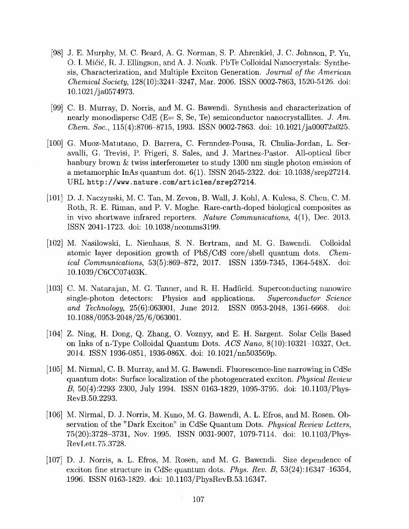
[98] J. E. Murphy, M. C. Beard, A. G. Norman, S. P. Ahrenkiel, J. C. Johnson, P. Yu,0. I. Midid, R. J. Ellingson, and A. J. Nozik. PbTe Colloidal Nanocrystals: Synthe-sis, Characterization, and Multiple Exciton Generation. Journal of the AmericanChemical Society, 128(10):3241-3247, Mar. 2006. ISSN 0002-7863, 1520-5126. doi:10.1021/ja0574973.
[99] C. B. Murray, D. Norris, and M. G. Bawendi. Synthesis and characterization ofnearly monodisperse CdE (E= S, Se, Te) semiconductor nanocrystallites. J. Am.Chem. Soc., 115(4):8706-8715, 1993. ISSN 0002-7863. doi: 10.1021/ja00072a025.
[100] G. Muoz-Matutano, D. Barrera, C. Fernndez-Pousa, R. Chulia-Jordan, L. Ser-avalli, G. Trevisi, P. Frigeri, S. Sales, and J. Martnez-Pastor. All-optical fiberhanbury brown & twiss interferometer to study 1300 nm single photon emission ofa metamorphic InAs quantum dot. 6(1). ISSN 2045-2322. doi: 10.1038/srep27214.URL http: //www. nature .com/articles/srep27214.
[101] D. J. Naczynski, M. C. Tan, M. Zevon, B. Wall, J. Kohl, A. Kulesa, S. Chen, C. M.Roth, R. E. Riman, and P. V. Moghe. Rare-earth-doped biological composites asin vivo shortwave infrared reporters. Nature Communications, 4(1), Dec. 2013.ISSN 2041-1723. doi: 10.1038/ncomms3l99.
[102] M. Nasilowski, L. Nienhaus, S. N. Bertram, and M. G. Bawendi. Colloidalatomic layer deposition growth of PbS/CdS core/shell quantum dots. Chem-ical Communications, 53(5):869-872, 2017. ISSN 1359-7345, 1364-548X. doi:10. 1039/C6CC07403K.
[103] C. M. Natarajan, M. G. Tanner, and R. H. Hadfield. Superconducting nanowiresingle-photon detectors: Physics and applications. Superconductor Scienceand Technology, 25(6):063001, June 2012. ISSN 0953-2048, 1361-6668. doi:10.1088/0953-2048/25/6/063001.
[104] Z. Ning, H. Dong, Q. Zhang, 0. Voznyy, and E. H. Sargent. Solar Cells Basedon Inks of n-Type Colloidal Quantum Dots. ACS Nano, 8(10):10321-10327, Oct.2014. ISSN 1936-0851, 1936-086X. doi: 10.1021/nn503569p.
[105] M. Nirmal, C. B. Murray, and M. G. Bawendi. Fluorescence-line narrowing in CdSequantum dots: Surface localization of the photogenerated exciton. Physical ReviewB, 50(4):2293-2300, July 1994. ISSN 0163-1829, 1095-3795. doi: 10.1103/Phys-RevB.50.2293.
[106] M. Nirmal, D. J. Norris, M. Kuno, M. G. Bawendi, A. L. Efros, and M. Rosen. Ob-servation of the "Dark Exciton" in CdSe Quantum Dots. Physical Review Letters,75(20):3728-3731, Nov. 1995. ISSN 0031-9007, 1079-7114. doi: 10.1103/Phys-RevLett.75.3728.
[107] D. J. Norris, a. L. Efros, M. Rosen, and M. G. Bawendi. Size dependence ofexciton fine structure in CdSe quantum dots. Phys. Rev. B, 53(24):16347-16354,1996. ISSN 0163-1829. doi: 10.1103/PhysRevB.53.16347.
107

[108] K. Nose, T. Omata, and S. Otsuka-Yao-Matsuo. Colloidal Synthesis of TernaryCopper Indium Diselenide Quantum Dots and Their Optical Properties. J. Phys.Chem. C, 113(9):3455-3460, Mar. 2009. ISSN 1932-7447. doi: 10.1021/jp809398k.
[109] U. D. of State. Cj final determinations, 2019. URLhttps: //www.pmddtc. state. gov.
[110] F. Olbrich, J. H6schele, M. Mller, J. Kettler, S. Luca Portalupi, M. Paul, M. Jet-ter, and P. Michler. Polarization-entangled photons from an InGaAs-based quan-tum dot emitting in the telecom C-band. Applied Physics Letters, 111(13):133106,Sept. 2017. ISSN 0003-6951, 1077-3118. doi: 10.1063/1.4994145.
[111] F. Olbrich, J. H6schele, M. Paul, J. Kettler, S. L. Portalupi, M. Jetter, and P. Mich-ler. Single-photon and polarization-entangled photon emission from InAs quantumdots in the telecom C-band. In D. L. Andrews, J.-M. Nunzi, A. Ostendorf, andA. J. Bain, editors, Nanophotonics VI, page 32, Strasbourg, France, May 2018.SPIE. ISBN 978-1-5106-1870-1 978-1-5106-1871-8. doi: 10.1117/12.2306765.
[112] A. Olkhovets, R.-C. Hsu, A. Lipovskii, and F. W. Wise. Size-Dependent Temper-ature Variation of the Energy Gap in Lead-Salt Quantum Dots. Phys. Rev. Lett.,81(16):3539-3542, Oct. 1998. doi: 10.1103/PhysRevLett.81.3539.
[113] D. Oron, A. Aharoni, C. de Mello Donega, J. van Rijssel, A. Meijerink, andU. Banin. Universal Role of Discrete Acoustic Phonons in the Low-TemperatureOptical Emission of Colloidal Quantum Dots. Physical Review Letters, 102(17),Apr. 2009. ISSN 0031-9007, 1079-7114. doi: 10.1103/PhysRevLett.102.177402.
[114] J. J. Peterson and T. D. Krauss. Fluorescence Spectroscopy of Single Lead SulfideQuantum Dots. Nano Lett., 6(3):510-514, 2006. doi: 10.1021/n10525756.
[115] J. M. Pietryga, R. D. Schaller, D. Werder, M. H. Stewart, V. I. Klimov, and J. A.Hollingsworth. Pushing the Band Gap Envelope: Mid-Infrared Emitting ColloidalPbSe Quantum Dots. Journal of the American Chemical Society, 126(38):11752-1f753, Sept. 2004. ISSN 0002-7863, 1520-5126. doi: 10.1021/ja047659f.
[116] Research and Markets. Shortwave infrared (swir) market by scanning type (areascan and line scan), technology (cooled and uncooled), application (securitysurveillance, monitoring inspection, and detection), vertical, and geography -global forecast to 2024, 2019. URL https: //www. researchandmarkets. com.
[117] J. E. Riggs, Z. Guo, D. L. Carroll, and Y.-P. Sun. Strong luminescence of solu-bilized carbon nanotubes. 122(24):5879-5880. ISSN 0002-7863, 1520-5126. doi:10.1021/ja9942282. URL http: //pubs. acs. org/doi/abs/10. 1021/ja9942282.
[118] D. Rosenberg, A. J. Kerman, R. J. Molnar, and E. A. Dauler. High-speed and high-efficiency superconducting nanowire single photon detector ar-ray. 21(2):1440. ISSN 1094-4087. doi: 10.1364/OE.21.001440. URLhttps: //www. osapublishing. org/oe/abstract. cfm?uri=oe-21-2-1440.
108

[119] M. J. F. Rubinsztein-Dunlop, E. Thomsen, P. Jensen, and Halina. Highly effi-cient luminescence from a hybrid state found in strongly quantum confined PbSnanocrystals. Nanotechnology, 17(4):956-957, 2006. ISSN 0957-4484.
[120] L. K. Sagar, W. Walravens, J. Maes, P. Geiregat, and Z. Hens. HgSe/CdE (E = S,Se) Core/Shell Nanocrystals by Colloidal Atomic Layer Deposition. The Journalof Physical Chemistry C, 121(25):13816-13822, June 2017. ISSN 1932-7447, 1932-7455. doi: 10.1021/acs.jpcc.7b02803.
[121] C. Santori, D. Fattal, and Y. Yamamoto. Indistinguishable photons from a single-photon device. 419:4, 2002.
[122] C. Santori, D. Fattal, J. Vuckovic, G. Solomon, and Y. Yamamoto. Generation ofsingle photons and correlated photon pairs using InAs quantum dots. Fortschritteder Physik, 52(11-12):1180-1188, Nov. 2004. ISSN 0015-8208, 1521-3978. doi:10. 1002/prop.200410188.
[123] E. H. Sargent. Infrared photovoltaics made by solution processing. Nat. Photonics,3(6):325-331, 2009. ISSN 1749-4885. doi: 10.1038/nphoton.2009.89.
[124] 0. E. Semonin, J. C. Johnson, J. M. Luther, A. G. Midgett, A. J. Nozik, andM. C. Beard. Absolute photoluminescence quantum yields of IR-26 dye, PbS, andPbSe quantum dots. 1(16):2445-2450. ISSN 1948-7185. doi: 10.1021/jzO0830r.URL http: //pubs . ac s. org/do i /10. 1021/j z100830r.
[125] P. Senellart, G. Solomon, and A. White. High-performance semiconductorquantum-dot single-photon sources. Nature Nanotechnology, 12(11):1026-1039,Nov. 2017. ISSN 1748-3387, 1748-3395. doi: 10.1038/nnano.2017.218.
[126] C. Sinito, M. J. Fernee, S. V. Goupalov, P. Mulvaney, P. Tamarat, and B. Lou-nis. Tailoring the Exciton Fine Structure of Cadmium Selenide Nanocrystals withShape Anisotropy and Magnetic Field. ACS Nano, 8(11):11651-11656, Nov. 2014.ISSN 1936-0851, 1936-086X. doi: 10.1021/nn5049409.
[127] J. Steckel, S. Coe-Sullivan, V. Bulovid, and M. Bawendi. 1.3pm to 1.55pm Tun-able Electroluminescence from PbSe Quantum Dots Embedded within an OrganicDevice. Advanced Materials, 15(21):1862-1866, Nov. 2003. ISSN 0935-9648, 1521-4095. doi: 10.1002/adma.200305449.
[128] N. Stiirzl, S. Lebedkin, and M. M. Kappes. Revisiting the Laser Dye Styryl-13 Asa Reference Near-Infrared Fluorophore: Implications for the PhotoluminescenceQuantum Yields of Semiconducting Single-Walled Carbon Nanotubes. The Journalof Physical Chemistry A, 113(38):10238-10240, Sept. 2009. ISSN 1089-5639, 1520-5215. doi: 10.1021/jp905166s.
[129] G. J. Supran, K. W. Song, G. W. Hwang, R. E. Correa, J. Scherer, E. A.Dauler, Y. Shirasaki, M. G. Bawendi, and V. Bulovic. High-performanceshortwave-infrared light-emitting devices using core-shell (PbS-CdS) colloidal
109

quantum dots. Adv. Mater., 27(8):1437-1442, 2015. ISSN 15214095. doi:10.1002/adma.201404636.
[130] I. Sychugov, A. Galeckas, N. Elfstrm, A. R. Wilkinson, R. G. Elliman, andJ. Linnros. Effect of substrate proximity on luminescence yield from si nanocrys-tals. 89(11):111124. ISSN 0003-6951, 1077-3118. doi: 10.1063/1.2226976. URLhttp://aip.scitation.org/doi/10.1063/1.2226976.
[131] M. C. Tan, J. Connolly, and R. E. Riman. Optical efficiency of short wave in-frared emitting phosphors. 115(36):17952-17957. ISSN 1932-7447, 1932-7455. doi:10.1021/jp203735n. URL http://pubs.acs.org/doi/10. 1021/jp203735n.
[132] J. Tang, K. W. Kemp, S. Hoogland, K. S. Jeong, H. Liu, L. Levina, M. Furukawa,X. Wang, R. Debnath, D. Cha, K. W. Chou, A. Fischer, A. Amassian, J. B.Asbury, and E. H. Sargent. Colloidal-quantum-dot photovoltaics using atomic-ligand passivation. Nat. Mater., 10(10):765-771, 2011. ISSN 1476-1122. doi:10.1038/nmat3118.
[133] E. Thimsen, B. Sadtler, and M. Y. Berezin. Shortwave-infrared (SWIR) emittersfor biological imaging: A review of challenges and opportunities. Nanophotonics,6(5):1043-1054, Aug. 2017. ISSN 2192-8614. doi: 10.1515/nanoph-2017-0039.
[134] N. J. Thompson, M. W. B. Wilson, D. N. Congreve, P. R. Brown, J. M. Scherer,T. S. Bischof, M. Wu, N. Geva, M. Welborn, T. V. Voorhis, V. Bulovi6, M. G.Bawendi, and M. A. Baldo. Energy harvesting of non-emissive triplet excitonsin tetracene by emissive PbS nanocrystals. Nat. Mater., 13(11):1039-1043, Nov.2014. ISSN 1476-1122.
[135] A. Tosi, A. D. Mora, F. Zappa, and S. Cova. Single-photon avalanche diodesfor the near-infrared range: Detector and circuit issues. Journal of Mod-ern Optics, 56(2-3):299-308, Jan. 2009. ISSN 0950-0340, 1362-3044. doi:10.1080/09500340802263075.
[136] A. Tosi, A. Della Frera, A. Bahgat Shehata, and C. Scarcella. Fullyprogrammable single-photon detection module for InGaAs/InP single-photonavalanche diodes with clean and sub-nanosecond gating transitions. Review ofScientific Instruments, 83(1):013104, Jan. 2012. ISSN 0034-6748, 1089-7623. doi:10.1063/1.3675579.
[137] L. Turyanska, A. Patane, M. Henini, B. Hennequin, and N. R. Thomas.Temperature dependence of the photoluminescence emission from thiol-cappedPbS quantum dots. Appl. Phys. Lett., 90(10):101913-101914, 2007. doi:http://dx.doi.org/10.1063/1.2711529.
[138] E. V. Ushakova, A. P. Litvin, P. S. Parfenov, A. V. Fedorov, M. Artemyev, A. V.Prudnikau, I. D. Rukhlenko, and A. V. Baranov. Anomalous Size-DependentDecay of Low-Energy Luminescence from PbS Quantum Dots in Colloidal Solution.ACS Nano, 6(10):8913-8921, Oct. 2012. ISSN 1936-0851. doi: 10.1021/nn3029106.
110

[139] M. C. Weidman, M. E. Beck, R. S. Hoffman, F. Prins, and W. A. Tisdale.Monodisperse, air-stable PbS nanocrystals via precursor stoichiometry control.8(6):6363-6371. ISSN 1936-0851, 1936-086X. doi: 10.1021/nn5018654. URLhttp://pubs.acs.org/doi/10.1021/nn5018654.
[140] M. C. Weidman, M. E. Beck, R. S. Hoffman, F. Prins, and W. A. Tisdale. Monodis-perse, Air-Stable PbS Nanocrystals via Precursor Stoichiometry Control. ACSNano, 8(6):6363-6371, June 2014. ISSN 1936-0851. doi: 10.1021/nn5018654.
[141] P. J. Whitham, K. E. Knowles, P. J. Reid, and D. R. Gamelin. Photolu-minescence Blinking and Reversible Electron Trapping in Copper-Doped CdSeNanocrystals. Nano Lett., 15(6):4045-4051, June 2015. ISSN 1530-6984. doi:10.1021/acs.nanolett.5b01046.
[142] R. H. Wilson, K. P. Nadeau, F. B. Jaworski, B. J. Tromberg, and A. J. Durkin.Review of short-wave infrared spectroscopy and imaging methods for biologicaltissue characterization. Journal of Biomedical Optics, 20:11, 2015.
[143] M. Wu, D. N. Congreve, M. W. B. Wilson, J. Jean, N. Geva, M. Welborn,T. Van Voorhis, V. Bulovi6, M. G. Bawendi, and M. A. Baldo. Solid-state infrared-to-visible upconversion sensitized by colloidal nanocrystals. Nat. Phot., 10(1):31-34, Jan. 2016. ISSN 1749-4885.
[144] Z. Yang, J. Z. Fan, A. H. Proppe, F. P. G. de Arquer, D. Rossouw, 0. Voznyy,X. Lan, M. Liu, G. Walters, R. Quintero-Bermudez, B. Sun, S. Hoogland, G. A.Botton, S. 0. Kelley, and E. H. Sargent. Mixed-quantum-dot solar cells. NatureCommunications, 8(1), Dec. 2017. ISSN 2041-1723. doi: 10.1038/s41467-017-01362-1.
[145] M. Yarema and M. V. Kovalenko. Colloidal Synthesis of InSb Nanocrystalswith Controlled Polymorphism Using Indium and Antimony Amides. Chem-istry of Materials, 25(9):1788-1792, May 2013. ISSN 0897-4756, 1520-5002. doi:10.1021/cm400320r.
[146] J. Zhang and X. Jiang. Confinement-Dependent Below-Gap State in PbS QuantumDot Films Probed by Continuous-Wave Photoinduced Absorption. J. Phys. Chem.B, 112(32):9557-9560, Aug. 2008. ISSN 1520-6106. doi: 10.1021/jp8047295.
[147] Y. Zhang, G. Hong, Y. Zhang, G. Chen, F. Li, H. Dai, and Q. Wang. Ag 2 SQuantum Dot: A Bright and Biocompatible Fluorescent Nanoprobe in the SecondNear-Infrared Window. ACS Nano, 6(5):3695-3702, May 2012. ISSN 1936-0851,1936-086X. doi: 10.1021/nn301218z.
[148] N. Zhao, T. P. Osedach, L.-Y. Chang, S. M. Geyer, D. Wanger, M. T. Binda, A. C.Arango, M. G. Bawendi, and V. Bulovic. Colloidal PbS Quantum Dot Solar Cellswith High Fill Factor. ACS Nano, 4(7):3743-3752, July 2010. ISSN 1936-0851.doi: 10.1021/nnO0129j.
111

[149] D. Zherebetskyy, M. Scheele, Y. Zhang, N. Bronstein, C. Thompson, D. Britt,M. Salmeron, P. Alivisatos, and L.-W. Wang. Hydroxylation of the surface of PbSnanocrystals passivated with oleic acid. Science, 344(6190):1380-1384, 2014. ISSN1095-9203. doi: 10.1126/science.1252727.
[150] D. Zhitomirsky, I. J. Kramer, A. J. Labelle, A. Fischer, R. Debnath, J. Pan, 0. M.Bakr, and E. H. Sargent. Colloidal Quantum Dot Photovoltaics: The Effect ofPolydispersity. Nano Lett., 12(2):1007-1012, Feb. 2012. ISSN 1530-6984. doi:10.1021/n2041589.
[151] Y. Zhong, Z. Ma, S. Zhu, J. Yue, M. Zhang, A. L. Antaris, J. Yuan, R. Cui,H. Wan, Y. Zhou, W. Wang, N. F. Huang, J. Luo, Z. Hu, and H. Dai. Boostingthe down-shifting luminescence of rare-earth nanocrystals for biological imagingbeyond 1500 nm. Nature Communications, 8(1), Dec. 2017. ISSN 2041-1723. doi:10. 1038/s41467-017-00917-6.
112