Resistive switching characteristics of Pt/CeOx/TiN memory device
6
This content has been downloaded from IOPscience. Please scroll down to see the full text. Download details: IP Address: 121.52.158.245 This content was downloaded on 27/04/2014 at 18:31 Please note that terms and conditions apply. Filament Evolution during Set and Reset Transitions in Oxide Resistive Switching Memory View the table of contents for this issue, or go to the journal homepage for more 2013 Jpn. J. Appl. Phys. 52 04CD10 (http://iopscience.iop.org/1347-4065/52/4S/04CD10) Home Search Collections Journals About Contact us My IOPscience
Transcript of Resistive switching characteristics of Pt/CeOx/TiN memory device

This content has been downloaded from IOPscience. Please scroll down to see the full text.
Download details:
IP Address: 121.52.158.245
This content was downloaded on 27/04/2014 at 18:31
Please note that terms and conditions apply.
Filament Evolution during Set and Reset Transitions in Oxide Resistive Switching Memory
View the table of contents for this issue, or go to the journal homepage for more
2013 Jpn. J. Appl. Phys. 52 04CD10
(http://iopscience.iop.org/1347-4065/52/4S/04CD10)
Home Search Collections Journals About Contact us My IOPscience

Filament Evolution during Set and Reset Transitions in Oxide Resistive Switching Memory
Daniele Ielmini1�, Simone Balatti1, and Stefano Larentis2
1Dipartimento di Elettronica e Informazione, Politecnico di Milano and IUNET, piazza L. da Vinci 32, I-20133 Milano (MI), Italy2Microelectronics Research Center, Department of Electrical and Computer Engineering, University of Texas at Austin,
10100 Burnet Rd., Austin, TX 78758, U.S.A.
E-mail: [email protected]
Received September 29, 2012; revised December 11, 2012; accepted January 22, 2013; published online April 22, 2013
Bipolar resistive switching memory (RRAM) relies on ion migration effects taking place at a conductive filament (CF). Understanding the evolution
of the CF during set and reset transitions is essential for predicting RRAM scalability and for developing new methods for storage and
computation. This work describes the evolution of the CF during bipolar resistive switching through numerical simulations of ion drift/diffusion. The
defect distribution profile for increasing current after set transition and for increasing voltage during set transition are shown. Finally, the
asymmetric shape of the CF is evidenced through polarity-dependent experiments and explained through numerical simulations.
# 2013 The Japan Society of Applied Physics
1. Introduction
Resistive switching phenomena in metal oxides are attract-ing a wide interest for their potential application in a novelclass of nonvolatile memories, the resistive switchingmemory (RRAM).1–3) Resistive switching offers fast, lowvoltage and low power programming4) combined withoutstanding cycling endurance.5) Bipolar switching inRRAM is based on the nanoionic formation/dissolution ofa conductive filament (CF), with diameter in the rangefrom 1 to 20 nm.6–8) The set transition, to achieve the lowresistance state, and the reset transition, to achieve the highresistance state, have opposite voltage polarities. Althoughthe nanoscale dimension of the CF is promising for RRAMscalability, a comprehensive understanding of the switchingmechanism is necessary to address issues such as thermalstability,8) programming variability,9) and current noise.10)
Toward this aim, an accurate physical picture of the CFnature and evolution during set/reset transitions in RRAM isessential.
This work discusses the bipolar switching characteristicsof oxide RRAM through a numerical model of ionmigration.11,12) We discuss the defect distribution profile inthe CF for increasing current in the set transition and forincreasing voltage in the reset transition. The asymmetricshape of the CF is evidenced through polarity-dependentmeasurements and explained by numerical simulation.The complementary switching (CS) phenomenon, observedunder positive voltage after a set transition under positivevoltage, is discussed.13) The overall good adherence of thesimulation results to the experimental data confirms the goodaccuracy of the ion migration model for RRAM.
2. Bipolar-Switching Characteristics
Figure 1 shows experimental current–voltage (I–V ) char-acteristics for RRAM devices with HfOx switching layersandwiched between TiN electrodes.14) The RRAM area was1 �m2 and the HfOx thickness was 20 nm. First, RRAMforming was achieved by dielectric breakdown of the HfOx
layer at about Vforming ¼ 2:2V. The forming operationallows to locally generate defects through thermally-inducedreduction of HfOx, thus leading to a Hf-rich CF withenhanced conductivity. A compliance current IC ¼ 0:2mAwas applied during forming, to avoid destructive breakdown.
The CF can be subsequently deactivated under negativevoltage, inducing the reset transition at Vreset ¼ �0:5V, andactivated again at a positive voltage Vset ¼ 0:6V with thesame compliance current adopted during forming. Note thatthe reset transition is gradual, in that the resistance continuesto increase for applied voltages above Vreset, while the settransition is generally abrupt.
Bipolar switching can be qualitatively understood by theschematic illustration in Fig. 2, showing the evolution ofthe CF from the high-resistance (reset) state to the lowresistance (set) state during the set transition. In the figure,blue dots represent conductive defects, such as oxygenvacancies and/or excess Hf atoms, which are generated at
VformingVset
IC
Ireset
Vreset
FormingSet
Reset
VC
Fig. 1. (Color online) Measured quasi-static I–V characteristics during
forming, set and reset transition for a HfOx RRAM devices.
Top electrode
Bottom electrode(a) (b) (c) (d)
Fig. 2. (Color online) Schematic illustration of the ion migration
phenomena at a CF during the set transition. Starting from the reset state,
obtained by reset under a negative voltage, the application of a positive
voltage results in the migration of positively-ionized defects (the blue dots
in the sketch) from the top reservoir into the gap (b–d).
Japanese Journal of Applied Physics 52 (2013) 04CD10
04CD10-1 # 2013 The Japan Society of Applied Physics
REGULAR PAPERhttp://dx.doi.org/10.7567/JJAP.52.04CD10

the initial forming (breakdown) operation. These conductivedefects are initially accumulated at the top electrode (TE),where they migrated in response to the negative voltageapplied to the TE in the preceding reset process. The CF isdisconnected due to the presence of a depleted gap with lowdefect-concentration, hence high resistivity. The applicationof a positive voltage to the TE during the set operationresults in the migration of the positively-ionized defectsfrom the top reservoir into the depleted gap, thus leading toa decrease of resistance. The abrupt set transition can beunderstood by noting that, as the depleted gap length � firstdecreases from (a) to (b) in Fig. 2 due to ion migration, thefield across the remaining gap increases. This accelerates ionmigration even further, causing the abrupt closure of thedepleted gap and the corresponding increase of the current inFig. 1. The reset transition proceeds right to left in Fig. 2, inthat the depleted gap gradually opens due to ion migrationtoward the TE. Opposite to the set transition, the migration-induced opening of the gap causes the decrease of theelectric field and of the temperature at the two tips of theCF.11) Due to such self-limited reset transition, the voltagemust be increased to achieve effective opening of the gapwithin the timescale of the experiment.
3. Nanoionic Drift/Diffusion Model
To better investigate the filament evolution during set andreset transitions in Fig. 1, we developed a numerical modelbased on the ionic drift-diffusion equation:11)
jD ¼ �DrnD þ �FnD; ð1Þdescribing the flow jD of ionized defects as a diffusion termdriven by the gradient of the defect concentration nD (firstterm on the right hand side in the equation) and a drift termdriven by the electric field F (second term on the right handside). Diffusion and drift are controlled by diffusivity D andmobility �, respectively, which were assumed to be linkedby the Einstein relation and to obey Arrhenius law withan activation energy EA ¼ 1 eV. Due to the temperatureactivation of D and �, Joule heating has a key role in theset/reset kinetics.11,15) The local temperature due to Jouleheating was computed solving the electrical and thermalconduction equations in the simulated structure. Theelectrical and thermal conductivities were assumed todepend linearly on the local dopant concentration, as aresult of the local change in free-carrier densities. Electrodeswere modeled as ideal from the point of view of electrical,thermal and ionic transport. Namely, the electrical boundarycondition at the electrodes was a constant electrostaticpotential, and the thermal boundary condition was a constanttemperature equal to room temperature (ideal heat sink). Noboundary thermal resistance or interface resistance wastaken into account. Finally, ion drift and diffusion wereassumed to take place only within the oxide, i.e., ion couldnot migrate to/from the electrodes.
Figure 3 shows the measured (a) and calculated (b) I–Vcurves during set and reset transitions for increasing IC ¼0:6, 1.1, and 1.5mA. The set state resistance R decreaseswith IC according to R / I�1
C , suggesting that the voltage VC
across the device is a fixed value at the end of the settransition (about 1 s in the quasi-static measurements andcalculations in the figure). The reset current Ireset, evaluated
at the reset voltage Vreset at the onset of the gradual resettransition (see Fig. 1), is approximately equal to IC, due toVreset � VC. These results indicate that set and resettransitions are driven by voltage, in that the ion migrationprocesses (namely, ionic drift, and diffusion) are driven bya strong (e.g., exponential) function of the voltage acrossthe device.12) This can be understood from the Arrheniusdependences for D and � in Eq. (1), where the localtemperature is controlled by the voltage across the cellthrough Joule heating.
3.1 Filament evolution during set transition
The control of resistance by IC in Fig. 3, which is useful formultilevel cell (MLC) applications, is due to the limitationof the CF effective size through the compliance system. Atthe onset of the set transition, the decrease of resistanceresults in a voltage snap-back to maintain the constantcurrent IC. The voltage decrease leads to a quenching of ionmigration kinetics, providing a negative feedback in theion-migration process. Irrespective of IC, the voltage acrossthe device reaches the value VC ¼ 0:4V, within the time-scale (� 1 s) of the quasi-static experiment.
Figure 4 shows the calculated map of defect (doping)concentration in the CF after the set transition in Fig. 3(b)for increasing IC. The initial state of the CF was a resetstate, obtained after reset transition on a cylindrical CF
IC = 1.5 mA
Set
1.1 mA
0.6 mA
Reset
(a) Measured
Set
Reset
(b) Calculated IC = 1.4 mA
1 mA
0.6 mA
Fig. 3. (Color online) Measured I–V curves during set and reset
transitions, for increasing IC (a) and corresponding calculated results (b).
For increasing IC, the resistance in the set state decreases while Iresetincreases.
D. Ielmini et al.Jpn. J. Appl. Phys. 52 (2013) 04CD10
04CD10-2 # 2013 The Japan Society of Applied Physics

with diameter � ¼ 14 nm at a maximum voltage of 0.8V(absolute value). The reset transition resulted in theformation of a depleted gap close to the bottom electrode(BE). For increasing IC, the doping concentration in thedepleted gap increases as a result of ion migration from thetop reservoir into the gap. The defect concentration in thegap increases for increasing IC in Fig. 4: this is because, forincreasing IC, the voltage snap-back occurs at decreasingCF resistance, corresponding to an increasing doping densityin the gap. These results suggest that the CF size extractedfrom the set-state resistance should be viewed as an effectivesize, describing not only the CF geometry but, mostimportantly, the defect concentration in the gap region.
3.2 Filament evolution during reset transition
MLC operation could also be achieved through the gradualreset transition in Fig. 3. To better understand the resettransition, Fig. 5 shows the measured and calculated I–Vcurves along the reset transition (a) and the contour plot ofthe doping concentration at different bias points for initialresistance values R ¼ 0:4 (b) and 1 k� (c). In Fig. 5, thedevice operation is assumed to be opposite to Figs. 1 and 2,i.e., set and reset transitions are obtained under negativeand positive voltage, respectively. As a result, ion migratetoward the bottom electrode [corresponding to z ¼ 0 inFigs. 5(b) and 5(c)] during the reset transition, due to thepositive voltage applied to the top electrode (z ¼ 20 nm inthe figure). The contour plot was computed at a dopingconcentration nD ¼ 0:6� 1021 cm�3 in Figs. 5(b) and 5(c).As initial state, we assumed an ideal set state withcylindrical shape and two different values of the diameter�, depending on the set state resistance, namely � ¼ 14
and 10 nm for R ¼ 0:4 and 1 k�, respectively. At Vreset,migration first induces gap nucleation close to the middle ofthe CF length, corresponding to the maximum temperatureobtained by Joule heating16) (see points B and B0). Forincreasing voltage after gap nucleation, the temperatureprofile changes due to the different profile of thermal andelectrical resistivities along the CF. In particular, moreheating is achieved at the depleted gap, while temperaturedecreases at the conductive regions of the CF. Due to thisquenching of the ion migration rate, further increase of thevoltage is needed to induce an increase of the gap length.
Contour plots at points C, C0, D, and D0 describe the gradualopening of the gap for increasing voltage.
After reaching the maximum voltage 1.1 V, the currentwas measured and calculated for decreasing voltage, tostudy the conduction characteristics in the reset state. Thisindicates a semiconductor-like transport mechanism, whichmight be due to Poole–Frenkel conduction.16) The calculatedI–V curve accounts for this feature by assuming a con-centration-dependent Poole–Frenkel barrier controlling theelectrical resistivity.11) It is worth noting that the reset stateresistance also depends on � in both experiments and
(a) (b) (c)
TE
BE
TE
BE
TE
BE
20
10
0
z [n
m]
r [nm]
0 10 20 30
r [nm]
0 10 20 30
r [nm]
0 10 20 30
0.7x10²¹
0nD [cm-3]
Fig. 4. (Color online) Calculated map of the defect distribution in the set state for increasing IC, namely IC ¼ 0:6, 1, and 1.4V. The defect density within
the depleted gap increases with IC, thus causing the observed decrease of R in Fig. 3.
A B C D
A’ B’ C’ D’
(a)
(b)
(c)
Fig. 5. (Color online) Measured and calculated I–V curves along the
reset transition (a) and contour plot of the defect density at increasing
voltage for R ¼ 0:4 (b) and 1 k� (c). The current is plotted as a function
of the absolute value of the voltage in (a). The contour plots (b, c) are
calculated for the bias points at increasing voltage indicated in the I–V
curves (a).
D. Ielmini et al.Jpn. J. Appl. Phys. 52 (2013) 04CD10
04CD10-3 # 2013 The Japan Society of Applied Physics
calculations, thus indicating a localized conduction in boththe set and reset states.14)
Figure 6 shows the measured and calculated reset times asa function of the device voltage. To measure the reset time, aconstant voltage V was applied to the cell in a set state ofabout R ¼ 0:2 k�, and the resistance increase was mon-itored. The reset time was defined in correspondence of the50% increase of resistance.11) For times larger than 10ms,voltage sweeps were applied instead of rectangular pulses.The reset times do not follow an exponential dependence onvoltage, while a clear exponential decrease if obtained in theArrhenius plot in the inset of Fig. 6, where the reset time isreported as a function of 1=kT . The local temperature T wasevaluated as the maximum temperature achieved along anideal (cylindrical) CF within the numerical simulation.These results evidence the key role of Joule heating inaccelerating the ion migration at the origin of set and resettransitions.4,12,15) The slight deviation of data from theexponential behavior in the Arrhenius plot can be explainedby the barrier lowering induced by the electric field in iontransport. Analytical models including the barrier loweringcan account for the curvature of reset time in the Arrheniusplot, where a smaller barrier EA leads to a smaller slope athigh voltage, hence high temperature.12)
4. Complementary Switching
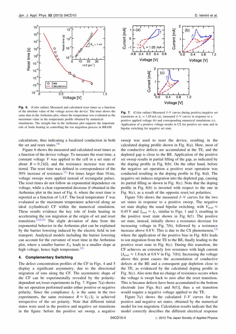
The defect concentration profiles of the CF in Figs. 4 and 5display a significant asymmetry, due to the directionalmigration of ions along the CF. The asymmetric shape ofthe CF can be experimentally revealed by the polarity-dependent set/reset experiments in Fig. 7. Figure 7(a) showsthe set operation performed under either positive or negativepolarity. Since the compliance IC is the same in the twoexperiments, the same resistance R � VC=IC is achievedirrespective of the set polarity. Note that different initialstates were used in the positive and negative set transitionsin the figure: before the positive set sweep, a negative
sweep was used to reset the device, resulting in thecalculated doping profile shown in Fig. 8(a). Here, most ofthe conductive defects are accumulated at the TE, and thedepleted gap is close to the BE. Application of the positiveset sweep results in partial filling of the gap, as indicated bythe doping profile in Fig. 8(b). On the other hand, beforethe negative set operation a positive reset operation wasconducted resulting in the doping profile in Fig. 8(d). Thenegative set induces migration into the depleted gap, causingits partial filling as shown in Fig. 8(c). Note that the dopingprofile in Fig. 8(b) is inverted with respect to the one inFig. 8(c), as a result of the opposite reset/set polarities.
Figure 7(b) shows the measured I–V curves for the twoset states in response to a positive sweep. The negativeset state display the usual bipolar switching, with Vreset �0:45V and Ireset � IC, similar to Figs. 1 and 3, resulting inthe positive reset state shown in Fig. 8(f ). The positiveset state, instead, initially shows a resistance decrease forincreasing voltage in Fig. 7(b), followed by a resistanceincrease above 0.8V. This is due to the CS phenomenon,13)
where the application of the positive bias in Fig. 8(b) leadsto ion migration from the TE to the BE, finally leading to thepositive reset state in Fig. 8(c). During this transition, theCF achieves an extremely low resistance with high current[Ireset � 1:8mA at 0.8V in Fig. 7(b)]. Increasing the voltageabove this point causes the accumulation of conductivedefects at the BE and a consequent gap depletion close tothe TE, as evidenced by the calculated doping profile inFig. 8(c). Also note that no change of resistance occurs whenthe voltage is swept back to zero after the reset transition.This is because defects have been accumulated to the bottomelectrode [see Figs. 8(c) and 8(f )], thus a set transitionwould require a negative voltage applied to the TE.
Figure 7(c) shows the calculated I–V curves for thepositive and negative set states, obtained by the numericalmodel for ion migration. Calculation results indicate that themodel correctly describes the different electrical response
Fig. 6. (Color online) Measured and calculated reset times as a function
of the absolute value of the voltage across the device. The inset shows the
same data in the Arrhenius plot, where the temperature was evaluated as the
maximum value in the temperature profile obtained by numerical
simulations. The straight line in the Arrhenius plot supports the important
role of Joule heating in controlling the ion migration process in RRAM.
(a) (b)
(c)
Fig. 7. (Color online) Measured I–V curves during positive/negative set
transitions at IC ¼ 1:05mA (a), measured I–V curves in response to a
positive applied voltage (b) and corresponding numerical simulations (c).
Application of a positive voltage results in CS for positive set state and in
bipolar switching for negative set state.
D. Ielmini et al.Jpn. J. Appl. Phys. 52 (2013) 04CD10
04CD10-4 # 2013 The Japan Society of Applied Physics

for different initial CF states. Figure 9 is a scatter plot of themeasured a calculated Ireset as a function of R. The differentresistive states were obtained by changing IC in the settransition [see Fig. 7(a)]. The reset current Ireset decreasesfor increasing R for negative set states. This is because thereset voltage Vreset remains practically constant irrespectiveof the CF effective size, due to the voltage-driven ionmigration kinetics.12) Therefore, given that Ireset ¼ Vreset=Rfor bipolar switching, the reset current is inversely propor-tional to R. Positive set state, instead, display CS, wherethe reset current corresponds to the maximum conductancestate, rather than the state achieved during the positive settransition. Since the minimum resistance is approximatelyconstant, the reset current do not depend on the initial setstate resistance. The good agreement between numericalsimulations and the data further supports the correctdescription of ion migration phenomena and of the filamentstates in the oxide RRAM.
5. Conclusions
We discussed the evolution of the filament shape and of thedefect distribution profile during set and reset switching inbipolar RRAM. Numerical simulations by an ionic drift-
diffusion model allow to provide microscopic interpretationsof the set state at different compliance current and of the resetstate at increasing voltage during the gradual reset transition.Finally, we discuss the different CF shapes depending on theset voltage polarity and the different electrical response to avoltage sweep, namely bipolar reset or CS.
Acknowledgments
We acknowledge SEMATECH for providing the experi-mental RRAM samples studied in this work. Fruitfuldiscussions with F. Nardi, K. Min, S. Koveshnikov, P.Spadini, D. Gilmer, and G. Bersuker are gratefully acknowl-edged. This work was supported in part by FondazioneCariplo (grant number 2010-0500) and Intel (contract55887).
1) T. W. Hickmott: J. Appl. Phys. 33 (1962) 2669.
2) F. Argall: Solid-State Electron. 11 (1968) 535.
3) J. F. Gibbons and W. E. Beadle: Solid-State Electron. 7 (1964) 785.
4) D. Ielmini: IEDM Tech. Dig., 2011, p. 409.
5) M.-J. Lee, C. B. Lee, D. Lee, S. R. Lee, M. Chang, J. H. Hur, Y.-B. Kim,
C.-J. Kim, D. H. Seo, S. Seo, U.-I. Chung, I.-K. Yoo, and K. Kim: Nat.
Mater. 10 (2011) 625.
6) D.-H. Kwon, K. M. Kim, J. H. Jang, J. M. Jeon, M. H. Lee, G. H. Kim,
X.-S. Li, G.-S. Park, B. Lee, S. Han, M. Kim, and C. S. Hwang: Nat.
Nanotechnol. 5 (2010) 148.
7) J. P. Strachan, M. D. Pickett, J. J. Yang, S. Aloni, A. L. D. Kilcoyne, G.
Medeiros-Ribeiro, and R. S. Williams: Adv. Mater. 22 (2010) 3573.
8) D. Ielmini, F. Nardi, C. Cagli, and A. L. Lacaita: IEEE Electron Device
Lett. 31 (2010) 353.
9) J. Park, M. Jo, E. M. Bourim, J. Yoon, D.-J. Seong, J. Lee, W. Lee, and H.
Hwang: IEEE Electron Device Lett. 31 (2010) 485.
10) D. Ielmini, F. Nardi, and C. Cagli: Appl. Phys. Lett. 96 (2010) 053503.
11) S. Larentis, F. Nardi, S. Balatti, D. C. Gilmer, and D. Ielmini: IEEE Trans.
Electron Devices 59 (2012) 2468.
12) D. Ielmini, F. Nardi, and S. Balatti: IEEE Trans. Electron Devices 59
(2012) 2049.
13) F. Nardi, S. Balatti, S. Larentis, D. C. Gilmer, and D. Ielmini: IEEE Trans.
Electron Devices 60 (2013) 70.
14) F. Nardi, S. Larentis, S. Balatti, D. C. Gilmer, and D. Ielmini: IEEE Trans.
Electron Devices 59 (2012) 2461.
15) S. Menzel, M. Waters, A. Marchewka, U. Bottger, R. Dittmann, and R.
Waser: Adv. Funct. Mater. 21 (2011) 4487.
16) D. Ielmini, C. Cagli, and F. Nardi: Nanotechnology 22 (2011) 254022.
(a) (b) (c) (d) (e) (f)
TE
BE
TE
BE
20
10
0
z [n
m]
7 nm
Positive set
Positive reset
Negative set
Positive reset
0.7x10²¹
0nD [cm-3]
Fig. 8. (Color online) Calculated distribution of defects corresponding to the calculated I–V curves in Fig. 7(c). The left panel describes the positive set
transition from the initial negative reset state (a) to the positive set state (b). Application of a positive voltage as in Fig. 7(c) results in CS and accumulation of
ionized defects at the bottom electrode. The right panel describes the negative set transition from the initial positive reset state (d) to the negative set state (e).
In this case, the application of the positive voltage causes the usual bipolar reset transition to the positive reset state (f ).
Positive set
Negative set
Fig. 9. (Color online) Scatter plot of the measured and calculated Ireset as
a function of R, for states obtained after positive set and negative set
transitions.
D. Ielmini et al.Jpn. J. Appl. Phys. 52 (2013) 04CD10
04CD10-5 # 2013 The Japan Society of Applied Physics