Atomic structure of conducting nanofilaments in TiO2 resistive switching memory
6
Atomic structure of conducting nanofilaments in TiO 2 resistive switching memory Deok-Hwang Kwon 1 , Kyung Min Kim 1,2 , Jae Hyuck Jang 1 , Jong Myeong Jeon 1 , Min Hwan Lee 1,2 , Gun Hwan Kim 1,2 , Xiang-Shu Li 3 , Gyeong-Su Park 3 , Bora Lee 4 , Seungwu Han 1 , Miyoung Kim 1 * and Cheol Seong Hwang 1,2 * Resistance switching in metal oxides could form the basis for next-generation non-volatile memory. It has been argued that the current in the high-conductivity state of several technologically relevant oxide materials flows through localized filaments, but these filaments have been characterized only indirectly, limiting our understanding of the switching mechanism. Here, we use high-resolution transmission electron microscopy to probe directly the nanofilaments in a Pt/TiO 2 /Pt system during resistive switching. In situ current–voltage and low-temperature (130 K) conductivity measurements confirm that switching occurs by the formation and disruption of Ti n O 2n21 (or so-called Magne ´li phase) filaments. Knowledge of the composition, structure and dimensions of these filaments will provide a foundation for unravelling the full mechanism of resistance switching in oxide thin films, and help guide research into the stability and scalability of such films for applications. I nnovations in modern information technology are critically dependent on the development of denser, faster and less energy- consuming non-volatile memory (NVM) 1 . Charge-based mem- ories, such as dynamic random access memory (DRAM) and flash memory, will suffer from performance degradation as the scaling limit is approached 2 . The development of non-charge-based memory is therefore essential for extending Moore’s law over the few next decades. Among the many contenders for next-generation NVM based on a non-charge mechanism, resistance-switching random access memory (RRAM) has attracted increasing attention because of the advantages in its fabrication process as well as its out- standing device performance 3–6 . In addition, RRAM is also suitable for the three-dimensional stacking of memory layers, which can lead to the ultimate high-density memory 7 . RRAM is based on the reversible dielectric (soft) breakdown of an insulator, particularly metal oxides. From a microscopic point of view, resistance switching in various materials can be classified broadly into two different mechanisms 3,8 . In the valence-change mechanism, the creation and electromigration of oxygen vacancies induces the distribution of the carrier density and the valence states of cations. For example, it is convincingly demonstrated in ref. 9 that the oxygen vacancies in SrTiO 3 migrate through the dis- location network and affect the conductivity. The device driven by this mechanism usually shows bipolar behaviour, in which the con- ducting and insulating states are switched with opposite bias polarity. In the fuse–antifuse mechanism, in which the interplay between the thermal effect and the redox reaction in the filament and its vicinity has a crucial role, metallic filaments are created through the insulator matrix during the electroforming process, and are fused as a result of Joule heating and the electric field 10–14 . In the antifuse process, the Joule heating-assisted reduction recon- nects the filament. In this case, resistance switching can be achieved with only one bias polarity, and is thus termed unipolar switching behaviour. Among the various oxide materials demonstrating unipolar switching behaviour 5,10–12,15–19 , TiO 2 appears to be one of the most promising switching materials to use this switching mechanism 5,10–12,15,16 . Several materials also show both types of switching behaviours 20–22 . In both valence-change and fuse–antifuse mechanisms, many aspects of the switching behaviour can be understood by assuming that the current flows through localized filaments in the conducting state 11,13,16 . However, basic information about the conducting fila- ments, such as their composition, size and density, has been inferred only indirectly 23,24 . Consequently, it is very difficult to understand the resistance-switching phenomena in terms of detailed chemical pro- cesses. The low density of metallic filaments poses a significant hurdle to characterizing their physical properties 10 . In this study, extensive and careful high-resolution transmission electron microscopy (HRTEM) and electron diffraction analyses have shown that the conducting filaments in TiO 2 are composed of Ti n O 2n21 (mostly n ¼ 4 or 5), known as Magne ´li phases. In situ local current–voltage (I–V ) measurements in TEM indicate that this trans- formed structure can indeed constitute an electrical conduction path. The conductivity measurements at low temperature (130 K) and in situ switching experiments confirm that the overall resistance switch- ing was induced by the Magne ´li phase filaments. Electrical switching behaviour Three types of TiO 2 films were examined: pristine, SET and RESET samples. The pristine sample was prepared using plasma-enhanced atomic layer deposition of 40-nm-thick TiO 2 thin films followed by the deposition of a platinum electrode, as shown in Fig. 1a (see Methods). To switch the pristine metal–insulator–metal (MIM) sample to the conducting state (forming process), a negative bias is applied to the top electrode with an appropriate compliance current (Fig. 1b). The TiO 2 film in this low-resistance state is called the ‘SET’ sample. The scanning electron microscopy (SEM) image in Fig. 1c shows that a part of the platinum top electrode is 1 Department of Materials Science and Engineering, Seoul National University, Seoul 151-744, Korea, 2 Inter-university Semiconductor Research Center, Seoul National University, Seoul 151-744, Korea, 3 Analytical Research Laboratory, Samsung Advanced Institute of Technology, PO Box 111, Suwon 440-600, Korea, 4 Department of Physics, Ewha Womans University, Seoul 120-750, Korea. *e-mail: [email protected]; [email protected] ARTICLES PUBLISHED ONLINE: 17 JANUARY 2010 | DOI: 10.1038/NNANO.2009.456 NATURE NANOTECHNOLOGY | VOL 5 | FEBRUARY 2010 | www.nature.com/naturenanotechnology 148 © 2010 Macmillan Publishers Limited. All rights reserved.
-
Upload
independent -
Category
Documents
-
view
3 -
download
0
Transcript of Atomic structure of conducting nanofilaments in TiO2 resistive switching memory
Atomic structure of conducting nanofilamentsin TiO2 resistive switching memoryDeok-Hwang Kwon1, Kyung Min Kim1,2, Jae Hyuck Jang1, Jong Myeong Jeon1, Min Hwan Lee1,2,
Gun Hwan Kim1,2, Xiang-Shu Li3, Gyeong-Su Park3, Bora Lee4, Seungwu Han1, Miyoung Kim1* and
Cheol Seong Hwang1,2*
Resistance switching in metal oxides could form the basis for next-generation non-volatile memory. It has been arguedthat the current in the high-conductivity state of several technologically relevant oxide materials flows through localizedfilaments, but these filaments have been characterized only indirectly, limiting our understanding of the switchingmechanism. Here, we use high-resolution transmission electron microscopy to probe directly the nanofilaments in aPt/TiO2/Pt system during resistive switching. In situ current–voltage and low-temperature (�130 K) conductivitymeasurements confirm that switching occurs by the formation and disruption of TinO2n21 (or so-called Magneli phase)filaments. Knowledge of the composition, structure and dimensions of these filaments will provide a foundation forunravelling the full mechanism of resistance switching in oxide thin films, and help guide research into the stability andscalability of such films for applications.
Innovations in modern information technology are criticallydependent on the development of denser, faster and less energy-consuming non-volatile memory (NVM)1. Charge-based mem-
ories, such as dynamic random access memory (DRAM) and flashmemory, will suffer from performance degradation as the scalinglimit is approached2. The development of non-charge-basedmemory is therefore essential for extending Moore’s law over thefew next decades. Among the many contenders for next-generationNVM based on a non-charge mechanism, resistance-switchingrandom access memory (RRAM) has attracted increasing attentionbecause of the advantages in its fabrication process as well as its out-standing device performance3–6. In addition, RRAM is also suitablefor the three-dimensional stacking of memory layers, which can leadto the ultimate high-density memory7.
RRAM is based on the reversible dielectric (soft) breakdown ofan insulator, particularly metal oxides. From a microscopic pointof view, resistance switching in various materials can be classifiedbroadly into two different mechanisms3,8. In the valence-changemechanism, the creation and electromigration of oxygen vacanciesinduces the distribution of the carrier density and the valencestates of cations. For example, it is convincingly demonstrated inref. 9 that the oxygen vacancies in SrTiO3 migrate through the dis-location network and affect the conductivity. The device driven bythis mechanism usually shows bipolar behaviour, in which the con-ducting and insulating states are switched with opposite biaspolarity. In the fuse–antifuse mechanism, in which the interplaybetween the thermal effect and the redox reaction in the filamentand its vicinity has a crucial role, metallic filaments are createdthrough the insulator matrix during the electroforming process,and are fused as a result of Joule heating and the electric field10–14.In the antifuse process, the Joule heating-assisted reduction recon-nects the filament. In this case, resistance switching can be achievedwith only one bias polarity, and is thus termed unipolar switchingbehaviour. Among the various oxide materials demonstrating
unipolar switching behaviour5,10–12,15–19, TiO2 appears to be oneof the most promising switching materials to use this switchingmechanism5,10–12,15,16. Several materials also show both types ofswitching behaviours20–22.
In both valence-change and fuse–antifuse mechanisms, manyaspects of the switching behaviour can be understood by assumingthat the current flows through localized filaments in the conductingstate11,13,16. However, basic information about the conducting fila-ments, such as their composition, size and density, has been inferredonly indirectly23,24. Consequently, it is very difficult to understand theresistance-switching phenomena in terms of detailed chemical pro-cesses. The low density of metallic filaments poses a significanthurdle to characterizing their physical properties10. In this study,extensive and careful high-resolution transmission electronmicroscopy (HRTEM) and electron diffraction analyses have shownthat the conducting filaments in TiO2 are composed of TinO2n21(mostly n¼ 4 or 5), known as Magneli phases. In situ localcurrent–voltage (I–V) measurements in TEM indicate that this trans-formed structure can indeed constitute an electrical conduction path.The conductivity measurements at low temperature (�130 K) and insitu switching experiments confirm that the overall resistance switch-ing was induced by the Magneli phase filaments.
Electrical switching behaviourThree types of TiO2 films were examined: pristine, SET and RESETsamples. The pristine sample was prepared using plasma-enhancedatomic layer deposition of 40-nm-thick TiO2 thin films followed bythe deposition of a platinum electrode, as shown in Fig. 1a (seeMethods). To switch the pristine metal–insulator–metal (MIM)sample to the conducting state (forming process), a negative biasis applied to the top electrode with an appropriate compliancecurrent (Fig. 1b). The TiO2 film in this low-resistance state iscalled the ‘SET’ sample. The scanning electron microscopy (SEM)image in Fig. 1c shows that a part of the platinum top electrode is
1Department of Materials Science and Engineering, Seoul National University, Seoul 151-744, Korea, 2Inter-university Semiconductor Research Center, SeoulNational University, Seoul 151-744, Korea, 3Analytical Research Laboratory, Samsung Advanced Institute of Technology, PO Box 111, Suwon 440-600, Korea,4Department of Physics, Ewha Womans University, Seoul 120-750, Korea. *e-mail: [email protected]; [email protected]
ARTICLESPUBLISHED ONLINE: 17 JANUARY 2010 | DOI: 10.1038/NNANO.2009.456
NATURE NANOTECHNOLOGY | VOL 5 | FEBRUARY 2010 | www.nature.com/naturenanotechnology148
© 2010 Macmillan Publishers Limited. All rights reserved.
blown off after the forming process, as indicated by the black arrow.The small explosion is probably caused by the sudden evolution ofcompressed excess oxygen gas16. The blown-off region of thesample may correspond to a location where the strongest filamentshave developed, and was useful for identifying the filaments at theinitial stage of the present work (Supplementary Fig. S1). However,this part does not act as a current path in the following switchingprocess, because the top electrode is missing. Two of the capacitorstructures were electroformed in this manner. A negative bias wasfurther applied to one of the two electroformed structures to switchthe sample into a high-resistance state. The TiO2 film in this high-resistance state is called the ‘RESET’ sample. Details regarding resist-ance switching by means of the I–V sweeps are reported in ref. 11.
HRTEM observationThe electron diffraction (ED) patterns and fast Fourier transformed(FFT) micrographs of the HRTEM images from each sample wereexamined extensively to determine the crystallographic structureof the filaments and the remaining part of the TiO2 films. In thecase of the pristine TiO2 sample, the majority phase was identifiedas a meta-stable brookite structure (Supplementary Fig. S2), ratherthan a rutile or anatase structure. This is understandable, becausethe deposition conditions of the pristine sample were far from thethermodynamic stability condition, even with plasma applicationat a growth temperature of 250 8C. It is also noted that nanoscalenon-stoichiometric TiOx (x , 2) phases were pervasive throughoutthe thin films, determined by the FFT of local regions of a few nano-metres, although their volume ratio is relatively small.
The ED patterns from the SET and RESET samples, however, havefeatures clearly distinguishable from pristine TiO2. First, a substantialamount of the dielectric films was changed, in both cases, into therutile or anatase phases. Thermal heating during the I–V sweepsmight have triggered the transition to more stable phases. Second,ED spots with smaller scattering angles than those of the anatase
[101] spots appear. Because the anatase [101] spots, correspondingto a d-spacing of 0.351 nm, have the smallest observable diffractionangle in the ED patterns from stoichiometric TiO2 with the brookite,anatase and rutile structures, those extra diffraction spots are indica-tive of the presence of non-stoichiometric TinO2n21 (mostly n¼ 4 or5). (Possible diffraction spots that can be excited by multiple scatter-ing, both from the same grain and from separate grains, were carefullytraced and were not considered for further examination.) This isknown as a Magneli phase25. The Magneli phase is a defective struc-ture derived from the ideal rutile phase, and can be described by thetwo-dimensional rutile (121) slabs made from octahedral TiO6 withan n-layer thickness in the direction normal to the slab plane. Theadjacent two slabs were displaced by 1=2½0�11� to accommodate theoxygen deficiencies25. Therefore, the nth (121) plane constitutes anantiphase boundary, which is known as the crystallographic shearplane. It is also well known that most of these Magneli phases are met-allic conductors near room temperature26. Therefore, the presence ofa Magneli phase in the SET and RESET samples could be responsiblefor the observed resistance-switching behaviours.
Most Magneli structures, whether connected or disconnected inthe HRTEM images, were fairly straight in both SET and RESETsamples. This implies that most nanofilaments are normal to theelectrode; if the filaments deviate significantly from the vertical direc-tion, one should be able to observe an image of slant nanofilaments inHRTEM. This is reasonable, because the nanofilaments are likely tobe formed along the direction of applied electric fields, which is thenormal direction to the film surface in the planar MIM geometry.
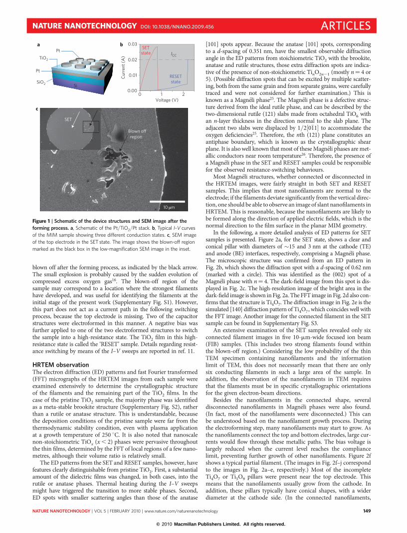
In the following, a more detailed analysis of ED patterns for SETsamples is presented. Figure 2a, for the SET state, shows a clear andconical pillar with diameters of �15 and 3 nm at the cathode (TE)and anode (BE) interfaces, respectively, comprising a Magneli phase.The microscopic structure was confirmed from an ED pattern inFig. 2b, which shows the diffraction spot with a d-spacing of 0.62 nm(marked with a circle). This was identified as the (002) spot of aMagneli phase with n¼ 4. The dark-field image from this spot is dis-played in Fig. 2c. The high-resolution image of the bright area in thedark-field image is shown in Fig. 2a. The FFT image in Fig. 2d also con-firms that the structure is Ti4O7. The diffraction image in Fig. 2e is thesimulated [140] diffraction pattern of Ti4O7, which coincides well withthe FFT image. Another image for the connected filament in the SETsample can be found in Supplementary Fig. S3.
An extensive examination of the SET samples revealed only sixconnected filament images in five 10-mm-wide focused ion beam(FIB) samples. (This includes two strong filaments found withinthe blown-off region.) Considering the low probability of the thinTEM specimen containing nanofilaments and the informationlimit of TEM, this does not necessarily mean that there are onlysix conducting filaments in such a large area of the sample. Inaddition, the observation of the nanofilaments in TEM requiresthat the filaments must be in specific crystallographic orientationsfor the given electron-beam directions.
Besides the nanofilaments in the connected shape, severaldisconnected nanofilaments in Magneli phases were also found.(In fact, most of the nanofilaments were disconnected.) This canbe understood based on the nanofilament growth process. Duringthe electroforming step, many nanofilaments may start to grow. Asthe nanofilaments connect the top and bottom electrodes, large cur-rents would flow through these metallic paths. The bias voltage islargely reduced when the current level reaches the compliancelimit, preventing further growth of other nanofilaments. Figure 2fshows a typical partial filament. (The images in Fig. 2f–j correspondto the images in Fig. 2a–e, respectively.) Most of the incompleteTi4O7 or Ti5O9 pillars were present near the top electrode. Thismeans that the nanofilaments usually grow from the cathode. Inaddition, these pillars typically have conical shapes, with a widerdiameter at the cathode side. (In the connected nanofilaments,
c
SET
Blown offregion
10 µm
TiO2
Pt
SiO2 Si
Pta b
0 1 20.00
0.01
0.02
0.03
Cur
rent
(A)
Voltage (V)
ICC
SETstate
RESETstate
Figure 1 | Schematic of the device structures and SEM image after the
forming process. a, Schematic of the Pt/TiO2/Pt stack. b, Typical I–V curves
of the MIM sample showing three different conduction states. c, SEM image
of the top electrode in the SET state. The image shows the blown-off region
marked as the black box in the low-magnification SEM image in the inset.
NATURE NANOTECHNOLOGY DOI: 10.1038/NNANO.2009.456 ARTICLES
NATURE NANOTECHNOLOGY | VOL 5 | FEBRUARY 2010 | www.nature.com/naturenanotechnology 149
© 2010 Macmillan Publishers Limited. All rights reserved.
three of the observed filaments have conical shapes; see Fig. 2a, Fig. 5cand Supplementary Fig. S3.) These findings are consistent with a fila-ment-growth model for TiO2 as already proposed11,15.
TEM analysis of the RESET samples indicates that they aresimilar to SET samples, except that no connected nanofilamentcould be found. In the RESET operation, the connected nanofila-ment should be ruptured, possibly by thermally assisted electromi-gration of oxygen ions10,11,15. However, disconnected nanofilamentswould not be affected by the RESET operation. (One of the discon-nected nanofilaments found in the RESET sample is shown inSupplementary Fig. S4.)
The observed filament diameters (measured at the middle pointalong the length) in the SET and RESET states ranged from 5 to10 nm, with the distance between them being between 0.1 and 5 mm(considering both connected and incomplete filaments). These areessential parameters for estimating the ultimate packing density ofthe RRAM device. The relatively large distances between filamentsare an unfavourable feature of the device, because this can comprise ascaling limit. However, it should be noted that once a filament is estab-lished, there would be no further filament formation in the adjacentregion, because the current flows mostly through the connected fila-ment. Therefore, even if the device size becomes very small, namely
� 100� 100 nm2, it is anticipated that there would be at least onefilament with which resistance switching could occur. In fact, a lowerdensity of filaments could be advantageous for device applications,because once a filament is formed in a nanoscale memory cell, it is unli-kely that another will form in the same cell. (Multiple filaments maydeteriorate the reproducibility of the resistance switching behaviour.)In this sense, a smaller cell size is conducive to better uniformity andrepeatability. Therefore, the size of the filament is a more importantparameter. The small size of the filaments suggests that the memorycell size can in principle be scaled down to tens of nanometres.
Even though the Magneli phase is a metal in the bulk phase, it isunclear whether the nano-sized Magneli pillar is also conducting.To establish this, the electrical conductivity of the Magneli nanofila-ments in the SET sample was measured using a local in situ I–Vscan in TEM (Fig. 3a) using the scanning tunnelling microscopy(STM) tip operating in conductive atomic force microscopy(CAFM) mode. The sample was prepared from the region where thetop electrode was blown off. Figure 3b shows the I–V curves obtainedfrom the Magneli structure (red circles) and from the area �50 nmaway from the filament where the Magneli structure was not identified(blue squares). The local I–V curve showed an electrical conductivityratio of �1,000 between the two locations. It was noted that the
TE
BE
(002)
a f
b c
d e
g h
i j
TE
BE
(002)
10 nm 10 nm
20 nm 20 nm
0.62 nm
2 nm−1 2 nm−1
0.62 nm
002
Ti4O7Ti4O7 [140]
413
002
Figure 2 | Magneli structures in the SET sample. a–e, High-resolution TEM image of a Ti4O7 nanofilament (a), selected-area diffraction pattern of the film
(b), dark-field image obtained from the diffraction spot marked as a circle in the diffraction pattern (c), a fast Fourier transformed micrograph of the high-
resolution image of Ti4O7 (d), and the corresponding simulated diffraction pattern (e). The Bloch-wave method was used to simulate the diffraction patterns.
f–j, Disconnected Ti4O7 structure in the conical shape. The images are presented in the same manner as for the connected filament in a–e.
ARTICLES NATURE NANOTECHNOLOGY DOI: 10.1038/NNANO.2009.456
NATURE NANOTECHNOLOGY | VOL 5 | FEBRUARY 2010 | www.nature.com/naturenanotechnology150
© 2010 Macmillan Publishers Limited. All rights reserved.

current variation due to the difference in probe pressure on the samplewas �15%, and there was a �10% difference with and without inci-dent high-energy electrons (for the TEM observation). The contactresistance might also complicate measurement of the absolute resist-ance values. However, the large conductivity ratio suggests that theobserved Magneli phases are indeed localized conducting paths. Inpassing, it is worth mentioning that there are three orders of differencein the current level between Figs 1b and 3b. This is because a largenumber of filaments contribute to the total current in the pad-typedevice in Fig. 1. In contrast, Fig. 3b was obtained for TEM samplesin which only one filament was probed.
Low-temperature measurementsAlthough TEM analysis in the above provided a clear observation of theMagneli phase filaments, it needs to be further confirmed that the nano-filaments are responsible for the conductivity in the SET state. This isbecause other parts of the TiO2 film, which may contain a largeportion of oxygen-deficient TiOx phase (or even metal atoms), mayalso contribute to electrical conduction27,28. To this end, the tempera-ture-dependent I–V curves of the MIM sample in the SET state weremeasured. It is known that the Magneli-structured Ti4O7 phase exhibitsa metal (high-temperature) to semiconductor (low-temperature) tran-sition at �150 K, with an abrupt drop in electrical conductivity by afactor of �1,000, caused by charge ordering of Ti3þ and Ti4þ ions29.Figure 4a shows the current values of the MIM sample measured at0.1 V with the temperature varying between 129.5 and 200 K. It isfound that the current drops sharply at 130 K. In Fig. 4b, the
corresponding I–V curves indicate that the conduction behaviourchanges from metallic to semiconducting (or insulating) near 130 K.(The I–V curve at 305 K was almost identical to that at 200 K.) Thisis similar to results reported for single-crystal Ti4O7 in ref. 29, exceptfor the transition temperature (130 K versus 150 K), and confirmsthat the electrical conduction in the SET state is governed by theMagneli nanofilaments. The discrepancy in the transition temperaturecould be ascribed to different correlation effects between the nanostruc-ture of the Magneli phase in the matrix of TiO2 and the single crystal.The I–V measurements at temperatures ranging from 313 to 363 K(data not shown) showed that the on-state resistance increases withthe temperature, which confirms metallic conduction in the SET state.
In situ switching in TEMTo further confirm that the observed structure and the accompanyingelectrical properties of Magneli phase nanofilaments are manipulatedby the applied voltage, an in situ RESET operation on a connectedMagneli structure was performed in TEM using the experimentalset-up shown in Fig. 5a. The STM tip approached the TE with theBE grounded. The Magneli structure of the connected nanofilamentwas confirmed (Fig. 5c) and then the I–V curve of the SET state wasobtained (red circles in Fig. 5b). The current density calculated fromFig. 5b reaches �1� 106 A cm22. Although this current density isnot high enough to induce elecromigration of atoms in the filament,the accompanying Joule heating effect may thermally anneal the fila-ment. An I–V sweep to a lower voltage (21.0 V) was then performedto reset the TEM sample. The I–V curve after the RESET operation
1 10 10010−1
100
101
102
103
baTi4O7
TiO2
Cur
rent
(nA
)
TiO2 Ti 4O 7
Pt
Voltage (mV)
Figure 3 | In situ I–V scan on nanofilaments. a, Schematic to show the experimental set-up. b, Local I–V curves measured on the Ti4O7 structure (red circles)
and on the anatase structure that is �50 nm away from the Ti4O7 (blue squares). The conductivity ratio between the two locations is �1,000.
0.1
1
10
a b
Cur
rent
(mA
at 0
.1 V
)
Temperature (K)
−10−0.4200 180 160 140 120 −0.2 0 0.2 0.4
−5
0
5
10 C
urre
nt (m
A)
Voltage (V)
Temp. (K) 200 180 160 150 145 132 130 129.5
Figure 4 | Temperature-dependent conduction behaviours of the MIM sample in the SET state. a, Current values measured at 0.1 V with the temperature
varying between 129.5 and 200 K. b, Corresponding I–V curves. The I–V curve at 305 K was almost identical to that of 200 K (not shown). It is found that
the sample changes its conduction behaviour from metallic (down to 132 K) to semiconducting (or insulating) at 130 and 129.5 K.
NATURE NANOTECHNOLOGY DOI: 10.1038/NNANO.2009.456 ARTICLES
NATURE NANOTECHNOLOGY | VOL 5 | FEBRUARY 2010 | www.nature.com/naturenanotechnology 151
© 2010 Macmillan Publishers Limited. All rights reserved.
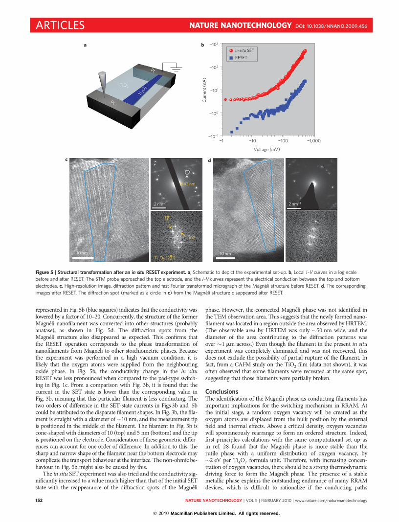
represented in Fig. 5b (blue squares) indicates that the conductivity waslowered by a factor of 10–20. Concurrently, the structure of the formerMagneli nanofilament was converted into other structures (probablyanatase), as shown in Fig. 5d. The diffraction spots from theMagneli structure also disappeared as expected. This confirms thatthe RESET operation corresponds to the phase transformation ofnanofilaments from Magneli to other stoichiometric phases. Becausethe experiment was performed in a high vacuum condition, it islikely that the oxygen atoms were supplied from the neighbouringoxide phase. In Fig. 5b, the conductivity change in the in situRESET was less pronounced when compared to the pad-type switch-ing in Fig. 1c. From a comparison with Fig. 3b, it is found that thecurrent in the SET state is lower than the corresponding value inFig. 3b, meaning that this particular filament is less conducting. Thetwo orders of difference in the SET-state currents in Figs 3b and 5bcould be attributed to the disparate filament shapes. In Fig. 3b, the fila-ment is straight with a diameter of �10 nm, and the measurement tipis positioned in the middle of the filament. The filament in Fig. 5b iscone-shaped with diameters of 10 (top) and 5 nm (bottom) and the tipis positioned on the electrode. Consideration of these geometric differ-ences can account for one order of difference. In addition to this, thesharp and narrow shape of the filament near the bottom electrode maycomplicate the transport behaviour at the interface. The non-ohmic be-haviour in Fig. 5b might also be caused by this.
The in situ SET experiment was also tried and the conductivity sig-nificantly increased to a value much higher than that of the initial SETstate with the reappearance of the diffraction spots of the Magneli
phase. However, the connected Magneli phase was not identified inthe TEM observation area. This suggests that the newly formed nano-filament was located in a region outside the area observed by HRTEM.(The observable area by HRTEM was only �50 nm wide, and thediameter of the area contributing to the diffraction patterns wasover �1 mm across.) Even though the filament in the present in situexperiment was completely eliminated and was not recovered, thisdoes not exclude the possibility of partial rupture of the filament. Infact, from a CAFM study on the TiO2 film (data not shown), it wasoften observed that some filaments were recreated at the same spot,suggesting that those filaments were partially broken.
ConclusionsThe identification of the Magneli phase as conducting filaments hasimportant implications for the switching mechanism in RRAM. Atthe initial stage, a random oxygen vacancy will be created as theoxygen atoms are displaced from the bulk position by the externalfield and thermal effects. Above a critical density, oxygen vacancieswill spontaneously rearrange to form an ordered structure. Indeed,first-principles calculations with the same computational set-up asin ref. 28 found that the Magneli phase is more stable than therutile phase with a uniform distribution of oxygen vacancy, by�2 eV per Ti4O7 formula unit. Therefore, with increasing concen-tration of oxygen vacancies, there should be a strong thermodynamicdriving force to form the Magneli phase. The presence of a stablemetallic phase explains the outstanding endurance of many RRAMdevices, which is difficult to rationalize if the conducting paths
−1 −10
a b
c d
−100 −1,000−10−1
−100
−101
−102
−103
In situ SETRESET
Cur
rent
(nA
)
Voltage (mV)
TiO2
Ti 4O 7
Pt
Pt
111
0.43 nm
102
Ti4O7 [231]10 nm 10 nm
2 nm−1 2 nm−1
Figure 5 | Structural transformation after an in situ RESET experiment. a, Schematic to depict the experimental set-up. b, Local I–V curves in a log scale
before and after RESET. The STM probe approached the top electrode, and the I–V curves represent the electrical conduction between the top and bottom
electrodes. c, High-resolution image, diffraction pattern and fast Fourier transformed micrograph of the Magneli structure before RESET. d, The corresponding
images after RESET. The diffraction spot (marked as a circle in c) from the Magneli structure disappeared after RESET.
ARTICLES NATURE NANOTECHNOLOGY DOI: 10.1038/NNANO.2009.456
NATURE NANOTECHNOLOGY | VOL 5 | FEBRUARY 2010 | www.nature.com/naturenanotechnology152
© 2010 Macmillan Publishers Limited. All rights reserved.
comprise a random distribution of point defects. In this respect, itwould be worth reexamining the conducting path in other oxidesin terms of vacancy ordering or oxygen-deficient phases. A recentreport on the valence reduction of a switching filament in CuOcells is, thus, very interesting30.
MethodsA 40-nm-thick TiO2 thin film was deposited on a 100-nm-thick sputteredplatinum/SiO2/silicon substrate by plasma-enhanced atomic layer deposition at250 8C using titanium tetraisopropoxide and plasma-activated O2 as the precursor andoxygen source, respectively. Structural and chemical characterization using grazing-angle incidence X-ray diffraction and X-ray photoelectron spectroscopy revealed theas-grown TiO2 film to have an amorphous to polycrystalline mixed anatase andbrookite structure with an oxygen/titanium ratio of �2.1. The grain shape wasgranular, and no specific preferred crystallographic orientation was observed.A 50-nm-thick circular platinum top electrode with a diameter of 300 mm was thenfabricated by electron-beam evaporation followed by a lift-off photolithographicprocess. The resistive switching behaviour of the MIM structure was measured at roomtemperature using an HP4145B semiconductor parameter analyser in the I–V sweepmode. The switching behaviour of the sample was measured by applying a negativebias voltage to the top electrode with the bottom electrode grounded. Two sampleswere electroformed using the I–V sweep with a compliance current of 20 mA. One ofthe two samples was set again to the high-resistance state by applying another reset I–V sweep. Therefore, SET samples experienced only one I–V sweep and the RESETsamples experienced two I–V sweeps. To confirm that the observed Magneli phasefilaments governs the overall resistive switching behaviour of the MIM sample, theconductance of the MIM sample in the SET state was measured at low temperature(down to 129.5 K) using a low-temperature stage of the CAFM (JEOL JSPM 5400) in ahigh-vacuum (1� 10–6 Torr) condition. A platinum-coated STM-type tip was used tominimize the contact resistance. The presence of intervening SiO2 below the MIMstructure adversely interferes with the fluent heat transfer between the MIM structureand the stage. To mitigate this problem, the TiO2 film surface was thermally connectedto the cold stage surface using silver paste.
The TEM specimens were prepared using a FIB etching technique to include thedielectrics directly under the top platinum electrode. A 300 kV field emission TEM(Jeol 3000F) and a 200 kV field emission TEM (Tecnai F20) were used for electrondiffraction, dark-field imaging and HRTEM. In situ localized I–V measurementsin Fig. 3 were performed on the Magneli structures, which were confirmed by ED andHRTEM before in situ experiments. A two-terminal I–V curve was measuredusing a double-tilt STM (Nanofactory Instruments AB, ST-1000) installed on a TEMholder of Tecnai F20G serving as a manipulator. I–V was measured in CAFMmode. The contact between the tungsten probe and the TiO2 sample was made usingthe STM unit, which could control the probe movement at sub-nanometreresolution with a piezotube. The integrity of the contact was constantly monitoredduring the I–V measurement. The TEM specimen for the in situ RESET experimentwas prepared by FIB from the SET sample, retaining both TE and BE, and negativebias was applied to the TE to keep the electrical bias direction the same as that inpad-type switching. The STM tip approached the TE instead of the TiO2 film to avoidinevitable specimen damage due to excessive heating related to the high contactresistance between the tip and TiO2. The connecting area between the top electrodeand the TEM copper grid was removed carefully by FIB in order to cut off the currentpath between the top and bottom electrodes through the copper grid.
Received 6 October 2009; accepted 25 November 2009;published online 17 January 2010
References1. Burr, G. W. et al. Overview of candidate device technologies for storage-class
memory. IBM J. Res. Dev. 52, 449–464 (2008).2. Waser, R. (ed.) Nanoelectronics and Information Technology Ch. 4
(Wiley-VCH, 2003).3. Waser, R. & Aono, M. Nanoionics-based resistive switching memories. Nature
Mater. 6, 833–840 (2007).4. Strukov, D. B., Snider, G. S., Stewart, D. R. & Williams, R. S. The missing
memristor found. Nature 453, 80–83 (2008).5. Seo, S. et al. Reproducible resistance switching in polycrystalline NiO films.
Appl. Phys. Lett. 85, 5655–5657 (2004).6. Meijer, G. I. Who wins the nonvolatile memory race? Science 319,
1625–1626 (2008).7. Likharev, K. K. & Strukov, D. B. Prospects for the development of digital circuits.
Proc. IEEE Int. Symp. Nanoscale Architectures 109–116, 2007.8. Sawa, A. Resistive switching in transition metal oxides. Mater. Today 11,
28–36 (2008).9. Szot, K., Speier, W., Bihlmayer, G. & Waser, R. Switching the electrical resistance
of individual dislocation in single-crystalline SrTiO3. Nature Mater. 5,312–320 (2006).
10. Choi, B. J. et al. Resistive switching mechanism of TiO2 thin films grown byatomic-layer-deposition. J. Appl. Phys. 98, 033715 (2005).
11. Kim, K. M., Choi, B. J., Shin, Y. C., Choi, S. & Hwang, C. S. Anode-interfacelocalized filamentary mechanism in resistive switching of TiO2 thin films.Appl. Phys. Lett. 91, 012907 (2007).
12. Rohde, C. et al. Identification of a determining parameter for resistive switchingof TiO2 thin films. Appl. Phys. Lett. 86, 262907 (2005).
13. Sato, Y., Kinoshita, K., Aoki, M. & Sugiyama, Y. Consideration of switchingmechanism of binary metal oxide resistive junctions using a thermal reactionmodel. Appl. Phys. Lett. 90, 033503 (2007).
14. Russo, U., Ielmini, D., Cagli, C. & Lacaita, A. L. Self-accelerated thermaldissolution model for reset programming in unipolar resistive-switchingmemory (RRAM) devices. IEEE Trans. Electron. Dev. 56, 193–200 (2009).
15. Kim, K. M. & Hwang, C. S. The conical shape filament growth model in unipolarresistance switching of TiO2 thin film. Appl. Phys. Lett. 94, 122109 (2009).
16. Jeong, D. S., Schroeder, H., Breuer, U. & Waser, R. Characteristic electroformingbehaviour in Pt/TiO2/Pt resistive switching cells depending on atmosphere.J. Appl. Phys. 104, 123716 (2008).
17. Shim, H. et al. Resistance-switching characteristics of polycrystalline Nb2O5 fornonvolatile memory application. IEEE Electron. Device Lett. 26, 292–294 (2005).
18. Lee, D. et al. Resistance switching of the nonstoichiometric zirconium oxide fornonvolatile memory applications. IEEE Electron. Device Lett. 26,719–721 (2005).
19. Kim, K. M. et al. Resistive switching in Pt/Al2O3/TiO2/Ru stacked structures.Electrochem. Solid State Lett. 9, G343–G346 (2006).
20. Jeong, D. S., Schroeder, H. & Waser, R. Coexistence of bipolar and unipolarresistive switching behaviors in a Pt/TiO2/Pt stack. Electrochem. Solid State Lett.10, G51–G53 (2007).
21. Lee, S., Kim, W.-G., Rhee, S.-W. & Yong, K. Resistance switching behaviors ofhafnium oxide films grown by MOCVD for nonvolatile memory applications.J. Electrochem. Soc. 155, H92–H96 (2008).
22. Yang, Y. C., Pan, F., Liu, Q., Liu, M. & Zeng, F. Fully room-temperature-fabricated nonvolatile resistive memory for ultrafast and high-density memoryapplication. Nano Lett. 9, 1636–1643 (2009).
23. Fujiwara, K. et al. Resistance switching and formation of a conductive bridge inmetal/binary oxide/metal structure for memory devices. Jpn J. Appl. Phys. 47,6266–6271 (2008).
24. Lee, M.-J. et al. Electrical manipulation of nanofilaments in transition-metaloxides for resistance-based memory. Nano Lett. 9, 1476–1481 (2009).
25. Bursill, L. A. & Hyde, B. G. Crystallographic shear in the higher titanium oxides:structure, texture, mechanisms and thermodynamics. Prog. Solid State Chem. 7,177–253 (1972).
26. Inglis, A. D., Page, Y. L., Strobel, P. & Hurd, C. M. Electrical conductance ofcrystalline TinO2n21 for n¼ 4–9. J. Phys. C 16, 317–333 (1983).
27. Yang, J. J. et al. Memristive switching mechanism for metal/oxide/metal nanodevices. Nature Nanotech. 3, 429–433 (2008).
28. Cho, E. et al. First-principles study of point defects in rutile TiO22x. Phys. Rev. B73, 193202 (2006).
29. Lakkis, S., Schlenker, C., Chakraverty, B. K., Buder, R. & Marezio, M. Metal–insulator transitions in Ti4O7 single crystals: crystal characterization, specificheat and electron paramagnetic resonance. Phys. Rev. B 14, 1429–1440 (1976).
30. Yasuhara, R. et al. Inhomogeneous chemical states in resistance-switchingdevices with a planar-type Pt/CuO/Pt structure. Appl. Phys. Lett. 95,012110 (2009).
AcknowledgementsThis work was supported by National Research Foundation of Korea grant funded by theMinistry of Education, Science and Technology (2009-0083038) and MEST-AFOSR NBITProgram. C.S.H., K.M.K., M.H.L. and K.H.K. acknowledge support by the NationalProgram for 0.1 Terabit NVM Devices of the Korean Government, the National ResearchFoundation of Korea (NRF) funded by the Ministry of Education, Science and Technology(grant no. 2009-0081961), and World Class University program through the Korea Scienceand Engineering Foundation funded by the Ministry of Education, Science and Technology(grant no. R31-2008-000-10075-0). B.L. and S.H. were supported by the QuantumMetamaterials Research Center (grant no. R11-2008-053-03001-0).
Author contributionsD.-H.K., J.H.J. and J.M.J. performed the TEM experiments and analysed the diffraction data.X.-S.L., G.-S.P. and D.-H.K. performed the in situ switching experiments in STM–TEM.K.M.K. and G.H.K. fabricated the samples and performed electrical switching experiments.M.H.L. performed the low temperature experiment. B.L. and S.H. performed the first-principles calculation. M.K. and C.S.H. conceived and designed the experiments. M.K., S.H.and C.S.H. co-wrote the paper. All authors discussed the results and commented onthe manuscript.
Additional informationThe authors declare no competing financial interests. Supplementary informationaccompanies this paper at www.nature.com/naturenanotechnology. Reprints andpermission information is available online at http://npg.nature.com/reprintsandpermissions/.Correspondence and requests for materials should be addressed to M.K. and C.S.H.
NATURE NANOTECHNOLOGY DOI: 10.1038/NNANO.2009.456 ARTICLES
NATURE NANOTECHNOLOGY | VOL 5 | FEBRUARY 2010 | www.nature.com/naturenanotechnology 153
© 2010 Macmillan Publishers Limited. All rights reserved.